US7041575B2 - Localized strained semiconductor on insulator - Google Patents
Localized strained semiconductor on insulatorDownload PDFInfo
- Publication number
- US7041575B2 US7041575B2US10/425,797US42579703AUS7041575B2US 7041575 B2US7041575 B2US 7041575B2US 42579703 AUS42579703 AUS 42579703AUS 7041575 B2US7041575 B2US 7041575B2
- Authority
- US
- United States
- Prior art keywords
- silicon
- region
- layer
- forming
- oxygen ions
- Prior art date
- Legal status (The legal status is an assumption and is not a legal conclusion. Google has not performed a legal analysis and makes no representation as to the accuracy of the status listed.)
- Expired - Lifetime
Links
- 239000004065semiconductorSubstances0.000titleclaimsabstractdescription108
- 239000012212insulatorSubstances0.000titleclaimsdescription49
- 238000000034methodMethods0.000claimsabstractdescription120
- 239000000758substrateSubstances0.000claimsabstractdescription112
- 229910052760oxygenInorganic materials0.000claimsabstractdescription103
- 239000001301oxygenSubstances0.000claimsabstractdescription103
- -1oxygen ionsChemical class0.000claimsabstractdescription64
- 210000000746body regionAnatomy0.000claimsabstractdescription17
- 229910052710siliconInorganic materials0.000claimsdescription190
- 239000010703siliconSubstances0.000claimsdescription190
- XUIMIQQOPSSXEZ-UHFFFAOYSA-NSiliconChemical compound[Si]XUIMIQQOPSSXEZ-UHFFFAOYSA-N0.000claimsdescription189
- 239000010410layerSubstances0.000claimsdescription173
- 230000008569processEffects0.000claimsdescription52
- QVGXLLKOCUKJST-UHFFFAOYSA-Natomic oxygenChemical compound[O]QVGXLLKOCUKJST-UHFFFAOYSA-N0.000claimsdescription41
- 239000007943implantSubstances0.000claimsdescription30
- 238000000137annealingMethods0.000claimsdescription25
- 239000002344surface layerSubstances0.000claimsdescription22
- 238000009792diffusion processMethods0.000claimsdescription21
- 238000002513implantationMethods0.000claimsdescription16
- 238000000926separation methodMethods0.000claimsdescription16
- 230000015572biosynthetic processEffects0.000claimsdescription6
- 238000010438heat treatmentMethods0.000claimsdescription3
- 239000012535impuritySubstances0.000claims1
- 229910000577Silicon-germaniumInorganic materials0.000description20
- 238000010586diagramMethods0.000description5
- 229910052732germaniumInorganic materials0.000description5
- 235000012431wafersNutrition0.000description5
- 230000008520organizationEffects0.000description4
- 238000004891communicationMethods0.000description3
- 238000005516engineering processMethods0.000description3
- 238000004519manufacturing processMethods0.000description3
- LEVVHYCKPQWKOP-UHFFFAOYSA-N[Si].[Ge]Chemical compound[Si].[Ge]LEVVHYCKPQWKOP-UHFFFAOYSA-N0.000description2
- 238000007796conventional methodMethods0.000description2
- 230000003247decreasing effectEffects0.000description2
- 230000007547defectEffects0.000description2
- 230000006870functionEffects0.000description2
- 238000005468ion implantationMethods0.000description2
- 239000000463materialSubstances0.000description2
- 230000003071parasitic effectEffects0.000description2
- 150000003376siliconChemical class0.000description2
- 238000000038ultrahigh vacuum chemical vapour depositionMethods0.000description2
- 230000006978adaptationEffects0.000description1
- 238000013459approachMethods0.000description1
- 230000008859changeEffects0.000description1
- 230000001351cycling effectEffects0.000description1
- 238000013461designMethods0.000description1
- 239000002019doping agentSubstances0.000description1
- 230000009977dual effectEffects0.000description1
- 239000011810insulating materialSubstances0.000description1
- 230000003993interactionEffects0.000description1
- 150000002500ionsChemical class0.000description1
- 210000003127kneeAnatomy0.000description1
- 239000012528membraneSubstances0.000description1
- 239000002086nanomaterialSubstances0.000description1
- 230000002093peripheral effectEffects0.000description1
- 238000000206photolithographyMethods0.000description1
- 238000004886process controlMethods0.000description1
- 238000012545processingMethods0.000description1
- 238000011160researchMethods0.000description1
- 238000007363ring formation reactionMethods0.000description1
Images


Classifications
- H—ELECTRICITY
- H01—ELECTRIC ELEMENTS
- H01L—SEMICONDUCTOR DEVICES NOT COVERED BY CLASS H10
- H01L21/00—Processes or apparatus adapted for the manufacture or treatment of semiconductor or solid state devices or of parts thereof
- H01L21/02—Manufacture or treatment of semiconductor devices or of parts thereof
- H01L21/04—Manufacture or treatment of semiconductor devices or of parts thereof the devices having potential barriers, e.g. a PN junction, depletion layer or carrier concentration layer
- H01L21/18—Manufacture or treatment of semiconductor devices or of parts thereof the devices having potential barriers, e.g. a PN junction, depletion layer or carrier concentration layer the devices having semiconductor bodies comprising elements of Group IV of the Periodic Table or AIIIBV compounds with or without impurities, e.g. doping materials
- H01L21/26—Bombardment with radiation
- H01L21/263—Bombardment with radiation with high-energy radiation
- H01L21/265—Bombardment with radiation with high-energy radiation producing ion implantation
- H01L21/26506—Bombardment with radiation with high-energy radiation producing ion implantation in group IV semiconductors
- H01L21/26533—Bombardment with radiation with high-energy radiation producing ion implantation in group IV semiconductors of electrically inactive species in silicon to make buried insulating layers
- H—ELECTRICITY
- H01—ELECTRIC ELEMENTS
- H01L—SEMICONDUCTOR DEVICES NOT COVERED BY CLASS H10
- H01L21/00—Processes or apparatus adapted for the manufacture or treatment of semiconductor or solid state devices or of parts thereof
- H01L21/70—Manufacture or treatment of devices consisting of a plurality of solid state components formed in or on a common substrate or of parts thereof; Manufacture of integrated circuit devices or of parts thereof
- H01L21/71—Manufacture of specific parts of devices defined in group H01L21/70
- H01L21/76—Making of isolation regions between components
- H01L21/762—Dielectric regions, e.g. EPIC dielectric isolation, LOCOS; Trench refilling techniques, SOI technology, use of channel stoppers
- H01L21/7624—Dielectric regions, e.g. EPIC dielectric isolation, LOCOS; Trench refilling techniques, SOI technology, use of channel stoppers using semiconductor on insulator [SOI] technology
- H01L21/76243—Dielectric regions, e.g. EPIC dielectric isolation, LOCOS; Trench refilling techniques, SOI technology, use of channel stoppers using semiconductor on insulator [SOI] technology using silicon implanted buried insulating layers, e.g. oxide layers, i.e. SIMOX techniques
- H—ELECTRICITY
- H10—SEMICONDUCTOR DEVICES; ELECTRIC SOLID-STATE DEVICES NOT OTHERWISE PROVIDED FOR
- H10D—INORGANIC ELECTRIC SEMICONDUCTOR DEVICES
- H10D30/00—Field-effect transistors [FET]
- H10D30/60—Insulated-gate field-effect transistors [IGFET]
- H10D30/791—Arrangements for exerting mechanical stress on the crystal lattice of the channel regions
- H—ELECTRICITY
- H10—SEMICONDUCTOR DEVICES; ELECTRIC SOLID-STATE DEVICES NOT OTHERWISE PROVIDED FOR
- H10D—INORGANIC ELECTRIC SEMICONDUCTOR DEVICES
- H10D62/00—Semiconductor bodies, or regions thereof, of devices having potential barriers
- H10D62/10—Shapes, relative sizes or dispositions of the regions of the semiconductor bodies; Shapes of the semiconductor bodies
- H10D62/17—Semiconductor regions connected to electrodes not carrying current to be rectified, amplified or switched, e.g. channel regions
- H10D62/213—Channel regions of field-effect devices
- H10D62/221—Channel regions of field-effect devices of FETs
- H10D62/235—Channel regions of field-effect devices of FETs of IGFETs
- H10D62/292—Non-planar channels of IGFETs
- H—ELECTRICITY
- H10—SEMICONDUCTOR DEVICES; ELECTRIC SOLID-STATE DEVICES NOT OTHERWISE PROVIDED FOR
- H10D—INORGANIC ELECTRIC SEMICONDUCTOR DEVICES
- H10D84/00—Integrated devices formed in or on semiconductor substrates that comprise only semiconducting layers, e.g. on Si wafers or on GaAs-on-Si wafers
- H10D84/01—Manufacture or treatment
- H10D84/0123—Integrating together multiple components covered by H10D12/00 or H10D30/00, e.g. integrating multiple IGBTs
- H10D84/0126—Integrating together multiple components covered by H10D12/00 or H10D30/00, e.g. integrating multiple IGBTs the components including insulated gates, e.g. IGFETs
- H10D84/0165—Integrating together multiple components covered by H10D12/00 or H10D30/00, e.g. integrating multiple IGBTs the components including insulated gates, e.g. IGFETs the components including complementary IGFETs, e.g. CMOS devices
- H10D84/0167—Manufacturing their channels
- H—ELECTRICITY
- H10—SEMICONDUCTOR DEVICES; ELECTRIC SOLID-STATE DEVICES NOT OTHERWISE PROVIDED FOR
- H10D—INORGANIC ELECTRIC SEMICONDUCTOR DEVICES
- H10D84/00—Integrated devices formed in or on semiconductor substrates that comprise only semiconducting layers, e.g. on Si wafers or on GaAs-on-Si wafers
- H10D84/01—Manufacture or treatment
- H10D84/02—Manufacture or treatment characterised by using material-based technologies
- H10D84/03—Manufacture or treatment characterised by using material-based technologies using Group IV technology, e.g. silicon technology or silicon-carbide [SiC] technology
- H10D84/038—Manufacture or treatment characterised by using material-based technologies using Group IV technology, e.g. silicon technology or silicon-carbide [SiC] technology using silicon technology, e.g. SiGe
Definitions
- This disclosurerelates generally to semiconductor structures, and more particularly, to strained semiconductor on insulator structures.
- strained silicon and silicon on insulator technologiesTwo areas of interest for improving the speed and performance of semiconductor devices include strained silicon and silicon on insulator technologies. Strained silicon technology has been shown to enhance carrier mobility in both n and p-channel devices, and is being considered to improve the electron mobility and drift velocity in n-channel MOSFET's in CMOS technology. Silicon on insulator structures have been shown to reduce parasitic capacitances, and to increase switching speed of digital circuits and frequency in radio frequency (RF) circuits.
- RFradio frequency
- One technique for producing strained siliconinvolves growing silicon (Si) layers on relaxed silicon-germanium (SiGe) layers.
- Sisilicon
- SiGerelaxed silicon-germanium
- a large mismatch in the cell structure between the Si and SiGe layerscauses a pseudo-morphic layer of Si on relaxed SiGe to be under biaxial tensile strain.
- the biaxial strainmodifies the band structure and enhances carrier transport in the Si layer. For example, a 1% strain of the silicon layer almost doubles the electron mobility.
- One method for forming the strained Si layer on the relaxed SiGe layerinvolves epitaxially growing the Si and SiGe layers using an ultra-high vacuum chemical vapor deposition (UHVCVD) process, and is a costly and complex process.
- UHVCVDultra-high vacuum chemical vapor deposition
- a proposed back end approach for straining siliconapplies uniaxial strain to wafers/dies after the integrated circuit process is complete.
- the diesare thinned to membrane dimensions and then affixed to curved substrates to apply an in-plane, tensile strain after device manufacture.
- Another method for straining siliconforms voids in a transistor structure to produce a localized mechanical strain in the silicon.
- One technique for fabricating a silicon-on-insulator structureinvolves a SIMOX (Separation by IMplantation of OXygen-Silicon-On-Insulator) process.
- the SIMOX processuses a very high dose and high energy oxygen implant followed by an oxide growth to form a deep and thick buried oxide (BOX) region.
- the SIMOX processtypically forms a BOX region 3000 ⁇ thick or thicker.
- the silicon layer over the BOX regionis typically 1000 ⁇ or thicker.
- Various embodiments of the present inventionrelate to strained semiconductor films along with the structures and devices that include strained semiconductor films.
- Various embodiments of the present inventionfurther relate to methods of forming the strained semiconductor films along with methods of forming structures and devices that include strained semiconductor films.
- One aspectrelates to a method for straining a transistor body region.
- oxygen ionsare implanted to a predetermined depth in a localized region of a semiconductor substrate, and the substrate is annealed.
- Oxide growth within the semiconductor substrateforms a local oxide region within the semiconductor substrate.
- a portion of the substrateforms a semiconductor layer over the local oxide region.
- the semiconductor layerhas a thickness of approximately 300 ⁇ or less.
- the oxide growthstrains the semiconductor layer.
- An active region, including the body region, of the transistoris formed in the strained semiconductor layer.
- One aspectrelates to a transistor structure.
- Various embodiments of the transistorinclude a semiconductor substrate, and a localized insulator region formed within the substrate to partially separate a semiconductor layer from the semiconductor substrate.
- the semiconductor layerhas a strain induced by growth of the insulator region.
- the strained semiconductor layerhaving a thickness of approximately 300 ⁇ or less.
- First and second diffusion regionsare formed in the strained semiconductor layer over the insulator region. The first and second diffusion regions are separated by a body region in the strained semiconductor layer.
- a gateis positioned over the body region, and is separated from the body region by a gate dielectric.
- the semiconductor substrateincludes a silicon substrate, the strained semiconductor layer includes a strained silicon layer, and the insulator region includes an oxide region.
- the oxide regionis formed using a SIMOX (Separation by IMplantation of OXygen) process.
- the oxide regionis formed using a SPIMOX (Separation by Plasma IMplantation of OXygen) process.
- Various embodimentsprovide ultra-thin strained silicon body layers for n-channel CMOS transistors. Shallow oxygen implants are formed in a localized area to produce pockets of oxide under a surface layer of silicon. The silicon above the oxide pocket is stretched and strained by a heat treatment process and a resulting oxide growth.
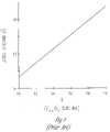
- FIG. 1illustrates the lattice constant of a Si 1-X -Ge X substrate for different percentages (X) of Ge.
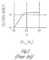
- FIG. 2illustrates the mobility enhancement for strained Si for different percentages (X) of Ge in a Si 1-X Ge X substrate.
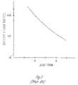
- FIG. 3illustrates a relationship between elastic strain and semiconductor layer thicknesses.
- FIG. 4illustrates a process for forming shallow oxygen implants such as is used in a process to produce strained silicon body layers for n-channel CMOS transistors, according to various embodiments of the present invention.
- FIG. 5illustrates a process for forming a buried oxide (BOX) region from the shallow oxygen implants such as is used in a process to produce strained silicon body layers for n-channel CMOS transistors, according to various embodiments of the present invention.
- BOXburied oxide
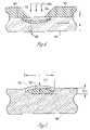
- FIGS. 6A and 6Billustrate the strain in the semiconductor layer achieved by the process to produce strained silicon body layers for n-channel CMOS transistors illustrated in FIGS. 4 and 5 .
- FIG. 7illustrates an n-channel CMOS transistor with a strained channel, according to various embodiments of the present invention.
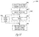
- FIG. 8illustrates a method for forming a device with an ultra-thin strained semiconductor layer, according to various embodiments of the present invention.
- FIG. 9illustrates a method for growing a local insulator area in a substrate, according to various embodiments of the present invention.
- FIG. 10illustrates a method for forming a device with an ultra-thin semiconductor layer with an approximate uniform strain, according to various embodiments of the present invention.
- FIG. 11is a simplified block diagram of a high-level organization of various embodiments of a memory device according to various embodiments of the present invention.
- FIG. 12is a simplified block diagram of a high-level organization of various embodiments of an electronic system according to the present invention.
- wafer and substrateare interchangeably used to refer generally to any structure on which integrated circuits are formed, and also to such structures during various stages of integrated circuit fabrication. Both terms include doped and undoped semiconductors, epitaxial layers of a semiconductor on a supporting semiconductor or insulating material, combinations of such layers, as well as other such structures that are known in the art.
- Various embodimentsprovide a local semiconductor structure with a strained semiconductor layer on insulator.
- Various embodimentsprovide strained silicon body layers for n-channel transistors.
- Various embodimentsprovide advantages for CMOS transistors because of the strained semiconductor on insulator structure.
- Various embodimentsprovide a technique to produce ultra-thin strained silicon body layers over a local insulator.
- Sisilicon
- SiGerelaxed silicon-germanium
- Gehas a lattice constant of 5.64613 ⁇ .
- the lattice constant of SiGeis between the lattice constant of Si and the lattice constant of Ge, and depends on the percentage of Ge in the SiGe layer.
- FIG. 1illustrates the lattice constant of a Si 1-X -Ge X substrate for different percentages (X) of Ge. As indicated by FIG. 1 , a Si 1-X Ge X substrate containing about 30% Ge (X ⁇ 0.3) has a lattice constant of about 5.50 ⁇ .
- the biaxial strain of the Si on the SiGecan be calculated as follows:
- Biaxial_StrainSiGe LC - Si LC Si LC , ( 1 ) where the subscript LC represents the lattice constant of the SiGe or Si.
- the Si on the SiGe substratehas a biaxial strain of about 1.28%.
- FIG. 2illustrates the mobility enhancement for strained Si for different percentages (X) of Ge in a Si 1-X Ge X substrate.
- the mobility enhancementincreases as the percentage of Ge in the Si 1-X Ge X increases, and levels off to around 1.6 when the percentage of Ge is around 22% or larger.
- 22% Geprovides the Si 1-X Ge X substrate with a lattice constant (SiGe LC ) of around 5.485.
- SiGe LClattice constant
- FIG. 3illustrates a relationship between elastic strain and semiconductor layer thicknesses.
- the semiconductor yieldis plotted with respect to plastic deformation and defects in bulk samples.
- the illustrated valuesrepresent the relationship of thin SiGe layers on silicon.
- FIG. 3illustrates that thin layers of silicon or other semiconductor materials are more tolerant of strain than thick bulk samples.
- thin layers of SiGehave been fabricated on silicon because of the tolerance of the thin layers to strain.
- FIG. 3indicates that 300 ⁇ thin semiconductor layers can be strained up to about 2%.
- the mobility enhancement levels off when the strainreaches about 1%.
- a thin semiconductor layer with a strain greater than 0.5%it is desirable to strain a thin semiconductor layer with a strain greater than 0.5% to achieve significant mobility enhancement. It is desirable to strain a thin semiconductor layer, such as an ultra-thin layer approximately 300 ⁇ . or less, with a strain within a range of approximately 0.75% to approximately 1.5% where the mobility enhancement levels off. It is also desirable to reduce unnecessary strain and provide a margin for error without unduly affecting the mobility enhancement. Thus, it is desirable to strain a thin semiconductor layer with a strain in the range of approximately 1% to approximately 1.2%.
- silicon on insulator structureshave been shown to reduce parasitic capacitances, and to increase switching speed of digital circuits and frequency in radio frequency (RF) circuits.
- One technique for fabricating a silicon-on-insulator structureinvolves a SIMOX (Separation by IMplantation of OXygen-Silicon-On-Insulator) process.
- the SIMOX processuses a very high dose and high energy oxygen implant followed by an oxide growth to form a deep and thick buried oxide (BOX) region.
- the BOX regionis typically 3000 ⁇ thick or thicker and the silicon layer over the BOX region is typically 1000 ⁇ or thicker when the SIMOX process has been used.
- the SIMOX processis an expensive process.
- siliconwas strained using localized SIMOX implants (line or ring formation), and epitaxial Ge was grown on the strained areas of the silicon.
- Epitaxial Gedoes not grow on normal silicon wafers because of the larger lattice constant of Ge.
- the resulting biaxial strain in the silicondid not match the Ge lattice constant, thus only small islands of Ge grew.
- Various embodiments of the present inventionmechanically strain a thin semiconductor layer and use the mechanically-strained semiconductor in an active region of a device.
- the thin semiconductor layeris also referred to herein as an ultra-thin semiconductor layer.
- Various ultra-thin semiconductor layer embodimentshave a thickness of approximately 300 ⁇ or less.
- the semiconductor layeris mechanically strained by growing a local insulator region to partially separate the semiconductor layer from a semiconductor substrate.
- the local insulator regionis formed underneath where the active region of the device is to be formed.
- the amount of strain in the semiconductor layer over the local insulator regionis controlled by controlling the size and shape of the insulator region.
- a silicon layeris mechanically strained by growing a local oxide region in a silicon substrate to partially separate the silicon layer from a silicon substrate.
- FIG. 4illustrates a process for forming shallow oxygen implants such as is used in a process to produce strained silicon body layers for n-channel CMOS transistors, according to various embodiments of the present invention.
- a mask 402is formed over a silicon substrate 404 to define a local area corresponding to a desired location of a transistor.
- Oxygen ionsare implanted, as represented by the arrows 406 , to form shallow oxygen implants 408 .
- the range (R), or depth, of the oxygen implantsis 300 ⁇ or less to form an ultra-thin, strained silicon body layer upon completion of the process.
- the illustrated process for forming the shallow oxygen implantsinvolves a SIMOX process.
- the layer thicknesses illustrated in FIG. 4are much thinner than conventional SIMOX processes.
- Conventional SIMOXuse very high dose and high energy implants, which can cause an unacceptable amount of damage in the silicon surface layer.
- a silicon layer over the BOX regionis typically 1000 ⁇ or thicker, and the BOX region is typically 3000 ⁇ thick. These dimensions correspond to a large volume of oxide and high oxygen dose, typically of the order 10 18 /cm 2 and energies of 180 KeV.
- the illustrated process for forming the shallow oxygen implantsinvolves a SPIMOX (Separation by Plasma Implantation of Oxygen-Silicon-On-Insulator) process.
- SPIMOXSeparatation by Plasma Implantation of Oxygen-Silicon-On-Insulator
- a SPIMOX processonly requires an oxygen dose of the order 10 17 /cm 2 and energies of 60 KeV.
- SIMOX and SPIMOX processesto form oxygen implants and produce strained body layers in accordance with the present subject matter.
- FIG. 5illustrates a process for forming a buried oxide (BOX) region from the shallow oxygen implants such as is used in a process to produce strained silicon body layers for n-channel CMOS transistors, according to various embodiments of the present invention.
- the substrate 504is heat treated or annealed such that an oxide pocket 510 , also referred to herein as a BOX region, is formed by the localized shallow oxygen implants 408 shown in FIG. 4 .
- the resulting oxide growthpartially separates a surface silicon layer 512 from the substrate 504 .
- the edges of the silicon layer 512remain attached to the substrate 504 .
- the growth of the BOX region 510strains this silicon layer 512 over the BOX region 510 .
- the illustrated silicon layer 512has a thickness T(Si), and the illustrated BOX region 510 has a thickness T(OX). Additionally, the footprint area of the BOX region 510 within the substrate 504 generally corresponds to the local area corresponding to the desired location of the transistor.
- the BOX region 510has a length L.
- the thickness of the silicon layeris an ultra-thin silicon layer corresponding to a thickness of 300 ⁇ or less.
- various embodimentsuse an oxide mask 402 with a tapered region or edge 414 proximate to the local area.
- the sloping oxide edge of the implant maskabsorbs some of the implanted oxygen such that fewer oxygen ions 406 penetrate the silicon substrate through the tapered region 414 , and those oxygen ions that do penetrate through the tapered region 414 penetrate the substrate 404 to a shallower depth, as represented by the portion 416 of the oxygen implants that extends closer to the substrate surface.
- the use of this tapered maskproduces a BOX region 510 with a tapered shape when the shallow oxygen implants 408 are annealed.
- the tapered mask and the implant processcan be engineered to provide a desired tapered shape of the resulting BOX region 510 to provide the silicon layer 512 over the BOX region 510 with a relatively uniform strain.
- FIGS. 6A and 6Billustrate the strain in the semiconductor layer achieved by the process to produce strained silicon body layers for n-channel CMOS transistors illustrated in FIGS. 4 and 5 .
- a BOX region 610is formed in the substrate 604 at an average distance of about 325 ⁇ under the substrate surface.
- the illustrated BOX region 610has a length (L) of approximately 3000 ⁇ and a thickness (T(OX)) of about 450 ⁇ , such that the BOX region 610 extends from approximately 100 ⁇ to 550 ⁇ below the substrate surface.
- T(OX)thickness
- the growth of the BOX regiondisplaces the 100 ⁇ surface layer of silicon upwards by about 225 ⁇ (1 ⁇ 2 of T(OX)).
- the original length of the silicon layerincreases by a change ( ⁇ ) corresponding to the strain induced in the silicon layer.
- ⁇the length of the silicon layer (1 ⁇ 2 of L) increases by a ⁇ (strain). If the distance to the edge of the BOX region is 1500 ⁇ (1 ⁇ 2 of L), then it can be calculated that a 1.1% strain of the silicon surface layer results from the growth of the illustrated BOX region 610 that has a thickness of approximately 450 ⁇ and a length of approximately 3000 ⁇ .
- various embodiments of the present inventionare capable of mechanically straining the ultra-thin silicon layer within the desired range of approximately 1% to approximately 1.2% to achieve a desired mobility enhancement with an appropriate margin for error and without unnecessarily straining the ultra-thin silicon layer.
- FIG. 7illustrates an n-channel CMOS transistor with a strained channel, according to various embodiments of the present invention.
- Conventional techniquescan be used to from n-channel CMOS transistors with a strained silicon channel.
- CMOS transistors with a strained silicon channelUpon reading and comprehending this disclosure, one of ordinary skill in the art will appreciate that the illustrated n-channel CMOS transistor is not drawn to scale, as the vertical dimensions have been expanded to better illustrate the structure.
- the illustrated structureincludes a silicon substrate 704 with a local BOX region 710 formed therein at a location corresponding to the desired location of the transistor.
- the formation of the BOX region 710partially separates a silicon layer 712 , which can also be referred to as a surface silicon layer, from the remainder of the silicon substrate 704 .
- This silicon layer 712is strained.
- the illustrated BOX region 710has a tapered shape, which provides an approximate uniform strain to the silicon layer 712 .
- Conventional techniquescan be used to form the transistor 720 using the locally strained and insulated silicon layer 712 .
- Diffusion regions 722 and 724are formed in the strained silicon layer 712 over the local BOX region 710 .
- the diffusion regionsare implanted with n+ dopants.
- a strained body region 726is between the diffusion regions 722 and 724 .
- a gate 728is operably positioned over and separated from the strained body region 726 by a gate dielectric 730 .
- the illustrated structureshows a word (WL) line connected to the gate 728 and a bit line (BL) connected to one of the diffusion regions 722 .
- the strained body region 726is formed in an ultra-thin silicon layer having a thickness of approximately 300 ⁇ or less. In various embodiments, the strained body region 726 is formed in an ultra-thin silicon layer having a thickness of approximately 100 ⁇ or less. In various embodiments, the strained body region 726 is formed in an ultra-thin silicon layer having a thickness of approximately 50 ⁇ or less. In various embodiments, the strained body region 726 is formed in an ultra-thin silicon layer having a thickness within a range of approximately 20 ⁇ to approximately 30 ⁇ .
- FIG. 8illustrates a method for forming a device with an ultra-thin strained semiconductor layer, according to various embodiments of the present invention.
- a local insulator areasuch as an oxide region
- a gate dielectric and a gateare operably formed over the strained semiconductor layer. Formation of the diffusion regions at 844 and the gate dielectric and gate at 846 form a transistor using the strained semiconductor layer, as generally represented at 848 .
- FIG. 9illustrates a method for growing a local insulator area in a substrate, according to various embodiments of the present invention.
- a local insulator areais grown by implanting oxygen ions, as represented at 950 , and the substrate is annealed, as represented at 952 .
- Various embodimentsuse a SIMOX process, and various embodiments use a SPIMOX process to grow the local insulator area.
- FIG. 10illustrates a method for forming a device with an ultra-thin semiconductor layer with an approximate uniform strain, according to various embodiments of the present invention.
- a tapered maskis deposited on a substrate to define a local area where a transistor device is to be formed.
- a local insulator areais grown at 1042 .
- the local insulator areais grown by implanting oxygen ions into the local area of the substrate at 1050 , and annealing or heat-treating the substrate to grow an oxide at 1052 .
- the resulting growth of the oxideinduces a strain in a surface layer of silicon that is separated from the silicon substrate.
- the tapered maskis removed at an appropriate time in the process, and a transistor is formed using the resulting strained semiconductor layer at 1048 .
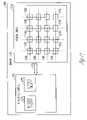
- FIG. 11is a simplified block diagram of a high-level organization of various embodiments of a memory device according to various embodiments of the present invention.
- the illustrated memory device 1168includes a memory array 1170 and read/write control circuitry 1172 to perform operations on the memory array via communication line(s) 1174 .
- the illustrated memory device 1168may be a memory card or a memory module such as a single inline memory module (SIMM) and dual inline memory module (DIMM).
- SIMMsingle inline memory module
- DIMMdual inline memory module
- semiconductor components in the memory array 1170 and/or the control circuitry 1172are able to be fabricated using the strained semiconductor films, as described above.
- the memory array 1170 and/or the control circuitry 1172include transistors with strained, ultra-thin body layers. The structure and fabrication methods for these strained, ultra-thin body layers have been described above.
- the memory array 1170includes a number of memory cells 1178 .
- the memory cells in the arrayare arranged in rows and columns.
- word lines 1180connect the memory cells in the rows
- bit lines 1182connect the memory cells in the columns.
- the read/write control circuitry 1172includes word line select circuitry 1174 , which functions to select a desired row.
- the read/write control circuitry 1172further includes bit line select circuitry 1176 , which functions to select a desired column.
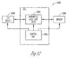
- FIG. 12is a simplified block diagram of a high-level organization of various embodiments of an electronic system according to the present invention.
- the system 1200is a computer system, a process control system or other system that employs a processor and associated memory.
- the electronic system 1200has functional elements, including a processor or arithmetic/logic unit (ALU) 1202 , a control unit 1204 , a memory device unit 1206 (such as illustrated in FIG. 11 ) and an input/output (I/O) device 1208 .
- ALUarithmetic/logic unit
- control unit 1204such as illustrated in FIG. 11
- I/Oinput/output
- Generally such an electronic system 1200will have a native set of instructions that specify operations to be performed on data by the processor 1202 and other interactions between the processor 1202 , the memory device unit 1206 and the I/O devices 1208 .
- the control unit 1204coordinates all operations of the processor 1202 , the memory device 1206 and the I/O devices 1208 by continuously cycling through a set of operations that cause instructions to be fetched from the memory device 1206 and executed.
- the memory device 1206includes, but is not limited to, random access memory (RAM) devices, read-only memory (ROM) devices, and peripheral devices such as a floppy disk drive and a compact disk CD-ROM drive.
- RAMrandom access memory
- ROMread-only memory
- peripheral devicessuch as a floppy disk drive and a compact disk CD-ROM drive.
- the illustration of the system 1200is intended to provide a general understanding of one application for the structure and circuitry using embodiments of the present invention, and is not intended to serve as a complete description of all the elements and features of an electronic system.
- an electronic systemcan be fabricated in single-package processing units, or even on a single semiconductor chip, in order to reduce the communication time between the processor and the memory device.
- Applications containing strained semiconductor films, such as transistors with a strained ultra-thin semiconductor body layer, as described in this disclosureinclude electronic systems for use in memory modules, device drivers, power modules, communication modems, processor modules, and application-specific modules, and may include multilayer, multichip modules. Such circuitry can further be a subcomponent of a variety of electronic systems.
- a locally strained semiconductor on a local insulator regionis provided.
- a SPIMOX or SIMOX processis used to form a local BOX region.
- a tapered maskis used to control the shape of the resulting BOX region to control the strain throughout the semiconductor layer.
- the locally strained semiconductor layeris used to form a transistor over the BOX region.
Landscapes
- Physics & Mathematics (AREA)
- Engineering & Computer Science (AREA)
- High Energy & Nuclear Physics (AREA)
- Condensed Matter Physics & Semiconductors (AREA)
- General Physics & Mathematics (AREA)
- Manufacturing & Machinery (AREA)
- Computer Hardware Design (AREA)
- Microelectronics & Electronic Packaging (AREA)
- Power Engineering (AREA)
- Health & Medical Sciences (AREA)
- Toxicology (AREA)
- Thin Film Transistor (AREA)
Abstract
Description
where the subscript LC represents the lattice constant of the SiGe or Si. Thus, as shown in
Claims (46)
Priority Applications (2)
| Application Number | Priority Date | Filing Date | Title |
|---|---|---|---|
| US10/425,797US7041575B2 (en) | 2003-04-29 | 2003-04-29 | Localized strained semiconductor on insulator |
| US10/931,554US7023051B2 (en) | 2003-04-29 | 2004-08-31 | Localized strained semiconductor on insulator |
Applications Claiming Priority (1)
| Application Number | Priority Date | Filing Date | Title |
|---|---|---|---|
| US10/425,797US7041575B2 (en) | 2003-04-29 | 2003-04-29 | Localized strained semiconductor on insulator |
Related Child Applications (1)
| Application Number | Title | Priority Date | Filing Date |
|---|---|---|---|
| US10/931,554DivisionUS7023051B2 (en) | 2003-04-29 | 2004-08-31 | Localized strained semiconductor on insulator |
Publications (2)
| Publication Number | Publication Date |
|---|---|
| US20040217391A1 US20040217391A1 (en) | 2004-11-04 |
| US7041575B2true US7041575B2 (en) | 2006-05-09 |
Family
ID=33309750
Family Applications (2)
| Application Number | Title | Priority Date | Filing Date |
|---|---|---|---|
| US10/425,797Expired - LifetimeUS7041575B2 (en) | 2003-04-29 | 2003-04-29 | Localized strained semiconductor on insulator |
| US10/931,554Expired - Fee RelatedUS7023051B2 (en) | 2003-04-29 | 2004-08-31 | Localized strained semiconductor on insulator |
Family Applications After (1)
| Application Number | Title | Priority Date | Filing Date |
|---|---|---|---|
| US10/931,554Expired - Fee RelatedUS7023051B2 (en) | 2003-04-29 | 2004-08-31 | Localized strained semiconductor on insulator |
Country Status (1)
| Country | Link |
|---|---|
| US (2) | US7041575B2 (en) |
Cited By (16)
| Publication number | Priority date | Publication date | Assignee | Title |
|---|---|---|---|---|
| US20040235264A1 (en)* | 2003-05-21 | 2004-11-25 | Micron Technology, Inc. | Gettering of silicon on insulator using relaxed silicon germanium epitaxial proximity layers |
| US20040232487A1 (en)* | 2003-05-21 | 2004-11-25 | Micron Technology, Inc. | Ultra-thin semiconductors bonded on glass substrates |
| US20050020094A1 (en)* | 2003-07-21 | 2005-01-27 | Micron Technology, Inc. | Strained semiconductor by full wafer bonding |
| US20050029619A1 (en)* | 2003-08-05 | 2005-02-10 | Micron Technology, Inc. | Strained Si/SiGe/SOI islands and processes of making same |
| US20050285139A1 (en)* | 2003-05-07 | 2005-12-29 | Micron Technology, Inc. | Strained Si/SiGe structures by ion implantation |
| US20060001094A1 (en)* | 2003-05-21 | 2006-01-05 | Micron Technology, Inc. | Semiconductor on insulator structure |
| US20060011982A1 (en)* | 2003-03-05 | 2006-01-19 | Micron Technology, Inc. | Micro-mechanically strained semiconductor film |
| US20060097281A1 (en)* | 2003-04-29 | 2006-05-11 | Micron Technology, Inc. | Strained semiconductor by wafer bonding with misorientation |
| US20060138541A1 (en)* | 2003-09-24 | 2006-06-29 | Fujitsu Limited | Semiconductor device and method of manufacturing same |
| US20070187683A1 (en)* | 2006-02-16 | 2007-08-16 | Micron Technology, Inc. | Localized compressive strained semiconductor |
| US20070190739A1 (en)* | 2006-02-15 | 2007-08-16 | Markus Zundel | Semiconductor having optimized insulation structure and process for producing the semiconductor |
| US20080029832A1 (en)* | 2006-08-03 | 2008-02-07 | Micron Technology, Inc. | Bonded strained semiconductor with a desired surface orientation and conductance direction |
| US20080029840A1 (en)* | 2006-08-02 | 2008-02-07 | Micron Technology, Inc. | Strained semiconductor, devices and systems and methods of formation |
| US20080042211A1 (en)* | 2006-08-18 | 2008-02-21 | Micron Technology, Inc. | Strained semiconductor channels and methods of formation |
| US20080050931A1 (en)* | 2004-03-31 | 2008-02-28 | International Business Machines Corporation | Method for fabricating strained silicon-on-insulator structures and strained silicon-on-insulator structures formed thereby |
| US7482190B2 (en) | 2003-05-07 | 2009-01-27 | Micron Technology, Inc. | Micromechanical strained semiconductor by wafer bonding |
Families Citing this family (31)
| Publication number | Priority date | Publication date | Assignee | Title |
|---|---|---|---|---|
| EP1441445B1 (en)* | 2003-01-24 | 2006-11-29 | STMicroelectronics S.r.l. | A pipeline analog-to-digital converter with correction of inter-stage gain errors |
| US7501329B2 (en) | 2003-05-21 | 2009-03-10 | Micron Technology, Inc. | Wafer gettering using relaxed silicon germanium epitaxial proximity layers |
| JP2005129676A (en)* | 2003-10-23 | 2005-05-19 | Sumitomo Mitsubishi Silicon Corp | Soi substrate, silicon substrate therefor and its manufacturing method |
| JP2005197405A (en)* | 2004-01-06 | 2005-07-21 | Toshiba Corp | Semiconductor device and manufacturing method thereof |
| US7518182B2 (en) | 2004-07-20 | 2009-04-14 | Micron Technology, Inc. | DRAM layout with vertical FETs and method of formation |
| US7285812B2 (en)* | 2004-09-02 | 2007-10-23 | Micron Technology, Inc. | Vertical transistors |
| US7199419B2 (en)* | 2004-12-13 | 2007-04-03 | Micron Technology, Inc. | Memory structure for reduced floating body effect |
| US7388278B2 (en) | 2005-03-24 | 2008-06-17 | International Business Machines Corporation | High performance field effect transistors on SOI substrate with stress-inducing material as buried insulator and methods |
| US20060226492A1 (en)* | 2005-03-30 | 2006-10-12 | Bich-Yen Nguyen | Semiconductor device featuring an arched structure strained semiconductor layer |
| US7371627B1 (en) | 2005-05-13 | 2008-05-13 | Micron Technology, Inc. | Memory array with ultra-thin etched pillar surround gate access transistors and buried data/bit lines |
| US7120046B1 (en) | 2005-05-13 | 2006-10-10 | Micron Technology, Inc. | Memory array with surrounding gate access transistors and capacitors with global and staggered local bit lines |
| US7888721B2 (en) | 2005-07-06 | 2011-02-15 | Micron Technology, Inc. | Surround gate access transistors with grown ultra-thin bodies |
| US7768051B2 (en) | 2005-07-25 | 2010-08-03 | Micron Technology, Inc. | DRAM including a vertical surround gate transistor |
| US7696567B2 (en) | 2005-08-31 | 2010-04-13 | Micron Technology, Inc | Semiconductor memory device |
| US7326601B2 (en)* | 2005-09-26 | 2008-02-05 | Advanced Micro Devices, Inc. | Methods for fabrication of a stressed MOS device |
| US7838387B2 (en)* | 2006-01-13 | 2010-11-23 | Sumco Corporation | Method for manufacturing SOI wafer |
| US20070224838A1 (en)* | 2006-03-27 | 2007-09-27 | Honeywell International Inc. | Method of straining a silicon island for mobility improvement |
| US20070228491A1 (en)* | 2006-04-04 | 2007-10-04 | Micron Technology, Inc. | Tunneling transistor with sublithographic channel |
| US7491995B2 (en) | 2006-04-04 | 2009-02-17 | Micron Technology, Inc. | DRAM with nanofin transistors |
| US7425491B2 (en)* | 2006-04-04 | 2008-09-16 | Micron Technology, Inc. | Nanowire transistor with surrounding gate |
| US8734583B2 (en)* | 2006-04-04 | 2014-05-27 | Micron Technology, Inc. | Grown nanofin transistors |
| US8354311B2 (en)* | 2006-04-04 | 2013-01-15 | Micron Technology, Inc. | Method for forming nanofin transistors |
| US7863141B2 (en)* | 2006-07-25 | 2011-01-04 | Chartered Semiconductor Manufacturing, Ltd. | Integration for buried epitaxial stressor |
| US7585711B2 (en)* | 2006-08-02 | 2009-09-08 | Taiwan Semiconductor Manufacturing Co., Ltd. | Semiconductor-on-insulator (SOI) strained active area transistor |
| US7557002B2 (en)* | 2006-08-18 | 2009-07-07 | Micron Technology, Inc. | Methods of forming transistor devices |
| US7989322B2 (en)* | 2007-02-07 | 2011-08-02 | Micron Technology, Inc. | Methods of forming transistors |
| US7759233B2 (en)* | 2007-03-23 | 2010-07-20 | Micron Technology, Inc. | Methods for stressing semiconductor material structures to improve electron and/or hole mobility of transistor channels fabricated therefrom, and semiconductor devices including such structures |
| US8293611B2 (en) | 2007-05-08 | 2012-10-23 | Micron Technology, Inc. | Implantation processes for straining transistor channels of semiconductor device structures and semiconductor devices with strained transistor channels |
| US7923373B2 (en) | 2007-06-04 | 2011-04-12 | Micron Technology, Inc. | Pitch multiplication using self-assembling materials |
| US7998815B2 (en)* | 2008-08-15 | 2011-08-16 | Qualcomm Incorporated | Shallow trench isolation |
| US9401363B2 (en) | 2011-08-23 | 2016-07-26 | Micron Technology, Inc. | Vertical transistor devices, memory arrays, and methods of forming vertical transistor devices |
Citations (62)
| Publication number | Priority date | Publication date | Assignee | Title |
|---|---|---|---|---|
| JPS54152464A (en) | 1978-05-22 | 1979-11-30 | Nec Corp | Preventing method for occurrence of crystal defect of silicon single-crystal substrate |
| JPS54155770A (en) | 1978-05-29 | 1979-12-08 | Nec Corp | Manufacture of semiconductor device |
| US4241359A (en) | 1977-11-28 | 1980-12-23 | Nippon Telegraph And Telephone Public Corporation | Semiconductor device having buried insulating layer |
| US4523975A (en) | 1982-04-19 | 1985-06-18 | Mitel Corporation | Integrated circuit planarizing process |
| US4962051A (en) | 1988-11-18 | 1990-10-09 | Motorola, Inc. | Method of forming a defect-free semiconductor layer on insulator |
| US5098852A (en) | 1989-07-05 | 1992-03-24 | Kabushiki Kaisha Toshiba | Method of manufacturing a semiconductor device by mega-electron volt ion implantation |
| US5461243A (en) | 1993-10-29 | 1995-10-24 | International Business Machines Corporation | Substrate for tensilely strained semiconductor |
| US5482869A (en) | 1993-03-01 | 1996-01-09 | Kabushiki Kaisha Toshiba | Gettering of unwanted metal impurity introduced into semiconductor substrate during trench formation |
| US5661044A (en) | 1993-11-24 | 1997-08-26 | Lockheed Martin Energy Systems, Inc. | Processing method for forming dislocation-free SOI and other materials for semiconductor use |
| US5673223A (en) | 1995-06-09 | 1997-09-30 | Samsung Electronics Co., Ltd. | Nonvolatile semiconductor memory device with multiple word line voltage generators |
| US5691230A (en) | 1996-09-04 | 1997-11-25 | Micron Technology, Inc. | Technique for producing small islands of silicon on insulator |
| US5854501A (en) | 1995-11-20 | 1998-12-29 | Micron Technology, Inc. | Floating gate semiconductor device having a portion formed with a recess |
| US5879996A (en) | 1996-09-18 | 1999-03-09 | Micron Technology, Inc. | Silicon-germanium devices for CMOS formed by ion implantation and solid phase epitaxial regrowth |
| US5963817A (en) | 1997-10-16 | 1999-10-05 | International Business Machines Corporation | Bulk and strained silicon on insulator using local selective oxidation |
| US5991225A (en) | 1998-02-27 | 1999-11-23 | Micron Technology, Inc. | Programmable memory address decode array with vertical transistors |
| US6093623A (en) | 1998-08-04 | 2000-07-25 | Micron Technology, Inc. | Methods for making silicon-on-insulator structures |
| US6136666A (en) | 1998-06-30 | 2000-10-24 | Hyundai Electronics Industries Co., Ltd. | Method for fabricating silicon-on-insulator wafer |
| US6162657A (en) | 1996-11-12 | 2000-12-19 | Fraunhofer-Gesellschaft Zur Forderung Der Angewandten Forschung E.V. | Method for manufacturing a micromechanical relay |
| US6180487B1 (en)* | 1999-10-25 | 2001-01-30 | Advanced Micro Devices, Inc. | Selective thinning of barrier oxide through masked SIMOX implant |
| US6204145B1 (en) | 1996-11-12 | 2001-03-20 | Micron Technology, Inc. | Silicon-on-insulator islands and method for their formation |
| US6228694B1 (en)* | 1999-06-28 | 2001-05-08 | Intel Corporation | Method of increasing the mobility of MOS transistors by use of localized stress regions |
| US6261876B1 (en)* | 1999-11-04 | 2001-07-17 | International Business Machines Corporation | Planar mixed SOI-bulk substrate for microelectronic applications |
| US6368938B1 (en) | 1999-10-05 | 2002-04-09 | Silicon Wafer Technologies, Inc. | Process for manufacturing a silicon-on-insulator substrate and semiconductor devices on said substrate |
| US6377070B1 (en) | 2001-02-09 | 2002-04-23 | Micron Technology, Inc. | In-service programmable logic arrays with ultra thin vertical body transistors |
| US6424001B1 (en) | 2001-02-09 | 2002-07-23 | Micron Technology, Inc. | Flash memory with ultra thin vertical body transistors |
| US6448601B1 (en) | 2001-02-09 | 2002-09-10 | Micron Technology, Inc. | Memory address and decode circuits with ultra thin body transistors |
| US6455397B1 (en) | 1999-11-16 | 2002-09-24 | Rona E. Belford | Method of producing strained microelectronic and/or optical integrated and discrete devices |
| US6461933B2 (en)* | 2000-12-30 | 2002-10-08 | Texas Instruments Incorporated | SPIMOX/SIMOX combination with ITOX option |
| US6486008B1 (en) | 2000-02-25 | 2002-11-26 | John Wolf International, Inc. | Manufacturing method of a thin film on a substrate |
| US6496034B2 (en) | 2001-02-09 | 2002-12-17 | Micron Technology, Inc. | Programmable logic arrays with ultra thin body transistors |
| US6515335B1 (en) | 2002-01-04 | 2003-02-04 | International Business Machines Corporation | Method for fabrication of relaxed SiGe buffer layers on silicon-on-insulators and structures containing the same |
| US6514836B2 (en) | 2001-06-04 | 2003-02-04 | Rona Elizabeth Belford | Methods of producing strained microelectronic and/or optical integrated and discrete devices |
| US6531727B2 (en) | 2001-02-09 | 2003-03-11 | Micron Technology, Inc. | Open bit line DRAM with ultra thin body transistors |
| US6541356B2 (en)* | 2001-05-21 | 2003-04-01 | International Business Machines Corporation | Ultimate SIMOX |
| US6559491B2 (en) | 2001-02-09 | 2003-05-06 | Micron Technology, Inc. | Folded bit line DRAM with ultra thin body transistors |
| US6566682B2 (en) | 2001-02-09 | 2003-05-20 | Micron Technology, Inc. | Programmable memory address and decode circuits with ultra thin vertical body transistors |
| US6583437B2 (en)* | 2000-03-17 | 2003-06-24 | Kabushiki Kaisha Toshiba | Semiconductor device and method of manufacturing the same |
| US6593625B2 (en) | 2001-06-12 | 2003-07-15 | International Business Machines Corporation | Relaxed SiGe layers on Si or silicon-on-insulator substrates by ion implantation and thermal annealing |
| US6597203B2 (en) | 2001-03-14 | 2003-07-22 | Micron Technology, Inc. | CMOS gate array with vertical transistors |
| US6649492B2 (en) | 2002-02-11 | 2003-11-18 | International Business Machines Corporation | Strained Si based layer made by UHV-CVD, and devices therein |
| US6649476B2 (en) | 2001-02-15 | 2003-11-18 | Micron Technology, Inc. | Monotonic dynamic-static pseudo-NMOS logic circuit and method of forming a logic gate array |
| US6656822B2 (en) | 1999-06-28 | 2003-12-02 | Intel Corporation | Method for reduced capacitance interconnect system using gaseous implants into the ILD |
| US20030227072A1 (en) | 2002-06-10 | 2003-12-11 | Leonard Forbes | Output prediction logic circuits with ultra-thin vertical transistors and methods of formation |
| US6689671B1 (en) | 2002-05-22 | 2004-02-10 | Advanced Micro Devices, Inc. | Low temperature solid-phase epitaxy fabrication process for MOS devices built on strained semiconductor substrate |
| US6703293B2 (en) | 2002-07-11 | 2004-03-09 | Sharp Laboratories Of America, Inc. | Implantation at elevated temperatures for amorphization re-crystallization of Si1-xGex films on silicon substrates |
| US6703648B1 (en) | 2002-10-29 | 2004-03-09 | Advanced Micro Devices, Inc. | Strained silicon PMOS having silicon germanium source/drain extensions and method for its fabrication |
| US6717216B1 (en) | 2002-12-12 | 2004-04-06 | International Business Machines Corporation | SOI based field effect transistor having a compressive film in undercut area under the channel and a method of making the device |
| US6740913B2 (en) | 1999-06-28 | 2004-05-25 | Intel Corporation | MOS transistor using mechanical stress to control short channel effects |
| US20040171196A1 (en) | 2002-08-08 | 2004-09-02 | Walitzki Hans J. | Method and apparatus for transferring a thin layer of semiconductor material |
| US20040173798A1 (en) | 2003-03-05 | 2004-09-09 | Micron Technology, Inc. | Micro-mechanically strained semiconductor film |
| US20040214366A1 (en) | 2001-07-25 | 2004-10-28 | Nantero, Inc. | Electromechanical memory array using nanotube ribbons and method for making same |
| US6812508B2 (en) | 2000-11-28 | 2004-11-02 | Sharp Kabushiki Kaisha | Semiconductor substrate and method for fabricating the same |
| US20040217352A1 (en) | 2003-04-29 | 2004-11-04 | Micron Technology, Inc. | Strained semiconductor by wafer bonding with misorientation |
| US20040224480A1 (en) | 2003-05-07 | 2004-11-11 | Micron Technology, Inc. | Micromechanical strained semiconductor by wafer bonding |
| US20040235264A1 (en) | 2003-05-21 | 2004-11-25 | Micron Technology, Inc. | Gettering of silicon on insulator using relaxed silicon germanium epitaxial proximity layers |
| US20040232487A1 (en) | 2003-05-21 | 2004-11-25 | Micron Technology, Inc. | Ultra-thin semiconductors bonded on glass substrates |
| US20040232488A1 (en) | 2003-05-21 | 2004-11-25 | Micron Technology, Inc. | Silicon oxycarbide substrates for bonded silicon on insulator |
| US20040232422A1 (en) | 2003-05-21 | 2004-11-25 | Micron Technology, Inc. | Wafer gettering using relaxed silicon germanium epitaxial proximity layers |
| US6825102B1 (en) | 2003-09-18 | 2004-11-30 | International Business Machines Corporation | Method of improving the quality of defective semiconductor material |
| US20050020094A1 (en) | 2003-07-21 | 2005-01-27 | Micron Technology, Inc. | Strained semiconductor by full wafer bonding |
| US20050017273A1 (en) | 2003-07-21 | 2005-01-27 | Micron Technology, Inc. | Gettering using voids formed by surface transformation |
| US20050029619A1 (en) | 2003-08-05 | 2005-02-10 | Micron Technology, Inc. | Strained Si/SiGe/SOI islands and processes of making same |
Family Cites Families (6)
| Publication number | Priority date | Publication date | Assignee | Title |
|---|---|---|---|---|
| US3953839A (en)* | 1975-04-10 | 1976-04-27 | International Business Machines Corporation | Bit circuitry for enhance-deplete ram |
| US5766053A (en) | 1995-02-10 | 1998-06-16 | Micron Technology, Inc. | Internal plate flat-panel field emission display |
| US6107661A (en) | 1995-09-29 | 2000-08-22 | Nippondenso Co., Ltd. | Semiconductor device and method of manufacturing same |
| FR2821483B1 (en) | 2001-02-28 | 2004-07-09 | St Microelectronics Sa | METHOD FOR MANUFACTURING A TRANSISTOR WITH INSULATED GRID AND ARCHITECTURE OF THE SUBSTRATE TYPE ON INSULATION, AND CORRESPONDING TRANSISTOR |
| US6855649B2 (en) | 2001-06-12 | 2005-02-15 | International Business Machines Corporation | Relaxed SiGe layers on Si or silicon-on-insulator substrates by ion implantation and thermal annealing |
| AU2002322105A1 (en) | 2001-06-14 | 2003-01-02 | Amberware Systems Corporation | Method of selective removal of sige alloys |
- 2003
- 2003-04-29USUS10/425,797patent/US7041575B2/ennot_activeExpired - Lifetime
- 2004
- 2004-08-31USUS10/931,554patent/US7023051B2/ennot_activeExpired - Fee Related
Patent Citations (72)
| Publication number | Priority date | Publication date | Assignee | Title |
|---|---|---|---|---|
| US4241359A (en) | 1977-11-28 | 1980-12-23 | Nippon Telegraph And Telephone Public Corporation | Semiconductor device having buried insulating layer |
| JPS54152464A (en) | 1978-05-22 | 1979-11-30 | Nec Corp | Preventing method for occurrence of crystal defect of silicon single-crystal substrate |
| JPS54155770A (en) | 1978-05-29 | 1979-12-08 | Nec Corp | Manufacture of semiconductor device |
| US4523975A (en) | 1982-04-19 | 1985-06-18 | Mitel Corporation | Integrated circuit planarizing process |
| US4962051A (en) | 1988-11-18 | 1990-10-09 | Motorola, Inc. | Method of forming a defect-free semiconductor layer on insulator |
| US5098852A (en) | 1989-07-05 | 1992-03-24 | Kabushiki Kaisha Toshiba | Method of manufacturing a semiconductor device by mega-electron volt ion implantation |
| US5482869A (en) | 1993-03-01 | 1996-01-09 | Kabushiki Kaisha Toshiba | Gettering of unwanted metal impurity introduced into semiconductor substrate during trench formation |
| US5759898A (en) | 1993-10-29 | 1998-06-02 | International Business Machines Corporation | Production of substrate for tensilely strained semiconductor |
| US5461243A (en) | 1993-10-29 | 1995-10-24 | International Business Machines Corporation | Substrate for tensilely strained semiconductor |
| US5661044A (en) | 1993-11-24 | 1997-08-26 | Lockheed Martin Energy Systems, Inc. | Processing method for forming dislocation-free SOI and other materials for semiconductor use |
| US5673223A (en) | 1995-06-09 | 1997-09-30 | Samsung Electronics Co., Ltd. | Nonvolatile semiconductor memory device with multiple word line voltage generators |
| US5854501A (en) | 1995-11-20 | 1998-12-29 | Micron Technology, Inc. | Floating gate semiconductor device having a portion formed with a recess |
| US6174784B1 (en) | 1996-09-04 | 2001-01-16 | Micron Technology, Inc. | Technique for producing small islands of silicon on insulator |
| US20020001965A1 (en) | 1996-09-04 | 2002-01-03 | Leonard Forbes | Technique for producing small islands of silicon on insulator |
| US5691230A (en) | 1996-09-04 | 1997-11-25 | Micron Technology, Inc. | Technique for producing small islands of silicon on insulator |
| US5879996A (en) | 1996-09-18 | 1999-03-09 | Micron Technology, Inc. | Silicon-germanium devices for CMOS formed by ion implantation and solid phase epitaxial regrowth |
| US6204145B1 (en) | 1996-11-12 | 2001-03-20 | Micron Technology, Inc. | Silicon-on-insulator islands and method for their formation |
| US6162657A (en) | 1996-11-12 | 2000-12-19 | Fraunhofer-Gesellschaft Zur Forderung Der Angewandten Forschung E.V. | Method for manufacturing a micromechanical relay |
| US6251751B1 (en) | 1997-10-16 | 2001-06-26 | International Business Machines Corporation | Bulk and strained silicon on insulator using local selective oxidation |
| US5963817A (en) | 1997-10-16 | 1999-10-05 | International Business Machines Corporation | Bulk and strained silicon on insulator using local selective oxidation |
| US5991225A (en) | 1998-02-27 | 1999-11-23 | Micron Technology, Inc. | Programmable memory address decode array with vertical transistors |
| US6136666A (en) | 1998-06-30 | 2000-10-24 | Hyundai Electronics Industries Co., Ltd. | Method for fabricating silicon-on-insulator wafer |
| US6093623A (en) | 1998-08-04 | 2000-07-25 | Micron Technology, Inc. | Methods for making silicon-on-insulator structures |
| US6538330B1 (en) | 1998-08-04 | 2003-03-25 | Micron Technology, Inc. | Multilevel semiconductor-on-insulator structures and circuits |
| US6309950B1 (en) | 1998-08-04 | 2001-10-30 | Micron Technology, Inc. | Methods for making silicon-on-insulator structures |
| US6228694B1 (en)* | 1999-06-28 | 2001-05-08 | Intel Corporation | Method of increasing the mobility of MOS transistors by use of localized stress regions |
| US6656822B2 (en) | 1999-06-28 | 2003-12-02 | Intel Corporation | Method for reduced capacitance interconnect system using gaseous implants into the ILD |
| US6740913B2 (en) | 1999-06-28 | 2004-05-25 | Intel Corporation | MOS transistor using mechanical stress to control short channel effects |
| US6368938B1 (en) | 1999-10-05 | 2002-04-09 | Silicon Wafer Technologies, Inc. | Process for manufacturing a silicon-on-insulator substrate and semiconductor devices on said substrate |
| US6180487B1 (en)* | 1999-10-25 | 2001-01-30 | Advanced Micro Devices, Inc. | Selective thinning of barrier oxide through masked SIMOX implant |
| US6261876B1 (en)* | 1999-11-04 | 2001-07-17 | International Business Machines Corporation | Planar mixed SOI-bulk substrate for microelectronic applications |
| US6455397B1 (en) | 1999-11-16 | 2002-09-24 | Rona E. Belford | Method of producing strained microelectronic and/or optical integrated and discrete devices |
| US6486008B1 (en) | 2000-02-25 | 2002-11-26 | John Wolf International, Inc. | Manufacturing method of a thin film on a substrate |
| US6583437B2 (en)* | 2000-03-17 | 2003-06-24 | Kabushiki Kaisha Toshiba | Semiconductor device and method of manufacturing the same |
| US6812508B2 (en) | 2000-11-28 | 2004-11-02 | Sharp Kabushiki Kaisha | Semiconductor substrate and method for fabricating the same |
| US6461933B2 (en)* | 2000-12-30 | 2002-10-08 | Texas Instruments Incorporated | SPIMOX/SIMOX combination with ITOX option |
| US6566682B2 (en) | 2001-02-09 | 2003-05-20 | Micron Technology, Inc. | Programmable memory address and decode circuits with ultra thin vertical body transistors |
| US6531727B2 (en) | 2001-02-09 | 2003-03-11 | Micron Technology, Inc. | Open bit line DRAM with ultra thin body transistors |
| US6559491B2 (en) | 2001-02-09 | 2003-05-06 | Micron Technology, Inc. | Folded bit line DRAM with ultra thin body transistors |
| US6496034B2 (en) | 2001-02-09 | 2002-12-17 | Micron Technology, Inc. | Programmable logic arrays with ultra thin body transistors |
| US6448601B1 (en) | 2001-02-09 | 2002-09-10 | Micron Technology, Inc. | Memory address and decode circuits with ultra thin body transistors |
| US6424001B1 (en) | 2001-02-09 | 2002-07-23 | Micron Technology, Inc. | Flash memory with ultra thin vertical body transistors |
| US6377070B1 (en) | 2001-02-09 | 2002-04-23 | Micron Technology, Inc. | In-service programmable logic arrays with ultra thin vertical body transistors |
| US6649476B2 (en) | 2001-02-15 | 2003-11-18 | Micron Technology, Inc. | Monotonic dynamic-static pseudo-NMOS logic circuit and method of forming a logic gate array |
| US6597203B2 (en) | 2001-03-14 | 2003-07-22 | Micron Technology, Inc. | CMOS gate array with vertical transistors |
| US6541356B2 (en)* | 2001-05-21 | 2003-04-01 | International Business Machines Corporation | Ultimate SIMOX |
| US6514836B2 (en) | 2001-06-04 | 2003-02-04 | Rona Elizabeth Belford | Methods of producing strained microelectronic and/or optical integrated and discrete devices |
| US6593625B2 (en) | 2001-06-12 | 2003-07-15 | International Business Machines Corporation | Relaxed SiGe layers on Si or silicon-on-insulator substrates by ion implantation and thermal annealing |
| US20040214366A1 (en) | 2001-07-25 | 2004-10-28 | Nantero, Inc. | Electromechanical memory array using nanotube ribbons and method for making same |
| US6515335B1 (en) | 2002-01-04 | 2003-02-04 | International Business Machines Corporation | Method for fabrication of relaxed SiGe buffer layers on silicon-on-insulators and structures containing the same |
| US6649492B2 (en) | 2002-02-11 | 2003-11-18 | International Business Machines Corporation | Strained Si based layer made by UHV-CVD, and devices therein |
| US6689671B1 (en) | 2002-05-22 | 2004-02-10 | Advanced Micro Devices, Inc. | Low temperature solid-phase epitaxy fabrication process for MOS devices built on strained semiconductor substrate |
| US20030227072A1 (en) | 2002-06-10 | 2003-12-11 | Leonard Forbes | Output prediction logic circuits with ultra-thin vertical transistors and methods of formation |
| US6703293B2 (en) | 2002-07-11 | 2004-03-09 | Sharp Laboratories Of America, Inc. | Implantation at elevated temperatures for amorphization re-crystallization of Si1-xGex films on silicon substrates |
| US20040171196A1 (en) | 2002-08-08 | 2004-09-02 | Walitzki Hans J. | Method and apparatus for transferring a thin layer of semiconductor material |
| US6703648B1 (en) | 2002-10-29 | 2004-03-09 | Advanced Micro Devices, Inc. | Strained silicon PMOS having silicon germanium source/drain extensions and method for its fabrication |
| US6717216B1 (en) | 2002-12-12 | 2004-04-06 | International Business Machines Corporation | SOI based field effect transistor having a compressive film in undercut area under the channel and a method of making the device |
| US20040173798A1 (en) | 2003-03-05 | 2004-09-09 | Micron Technology, Inc. | Micro-mechanically strained semiconductor film |
| US20050023529A1 (en) | 2003-04-29 | 2005-02-03 | Micron Technology, Inc. | Strained semiconductor by wafer bonding with misorientation |
| US20040217352A1 (en) | 2003-04-29 | 2004-11-04 | Micron Technology, Inc. | Strained semiconductor by wafer bonding with misorientation |
| US20040224480A1 (en) | 2003-05-07 | 2004-11-11 | Micron Technology, Inc. | Micromechanical strained semiconductor by wafer bonding |
| US20050032296A1 (en) | 2003-05-07 | 2005-02-10 | Micron Technology, Inc. | Micromechanical strained semiconductor by wafer bonding |
| US20040232487A1 (en) | 2003-05-21 | 2004-11-25 | Micron Technology, Inc. | Ultra-thin semiconductors bonded on glass substrates |
| US20040232488A1 (en) | 2003-05-21 | 2004-11-25 | Micron Technology, Inc. | Silicon oxycarbide substrates for bonded silicon on insulator |
| US20040232422A1 (en) | 2003-05-21 | 2004-11-25 | Micron Technology, Inc. | Wafer gettering using relaxed silicon germanium epitaxial proximity layers |
| US20050023612A1 (en) | 2003-05-21 | 2005-02-03 | Micron Technology, Inc. | Ultra-thin semiconductors bonded on glass substrates |
| US20040235264A1 (en) | 2003-05-21 | 2004-11-25 | Micron Technology, Inc. | Gettering of silicon on insulator using relaxed silicon germanium epitaxial proximity layers |
| US20050020094A1 (en) | 2003-07-21 | 2005-01-27 | Micron Technology, Inc. | Strained semiconductor by full wafer bonding |
| US20050017273A1 (en) | 2003-07-21 | 2005-01-27 | Micron Technology, Inc. | Gettering using voids formed by surface transformation |
| US20050029619A1 (en) | 2003-08-05 | 2005-02-10 | Micron Technology, Inc. | Strained Si/SiGe/SOI islands and processes of making same |
| US20050087842A1 (en) | 2003-08-05 | 2005-04-28 | Micron Technology, Inc. | Strained Si/SiGe/SOI islands and processes of making same |
| US6825102B1 (en) | 2003-09-18 | 2004-11-30 | International Business Machines Corporation | Method of improving the quality of defective semiconductor material |
Non-Patent Citations (50)
| Title |
|---|
| "Cornell Demonstrates a Universal Substrate", Compound Semiconductor, 3(2), (Mar./Apr. 1997),27-29. |
| Abe, T., "Silicon Wafer-Bonding Process Technology for SOI Structures", Extended Abstracts of the 22nd (1990 International) Conference on Solid State Devices and Materials, (1990),853-856. |
| Auberton-Herve, A J., "SOI: Materials to Systems", Digest of the International Electron Device Meeting, (1996), 1.1.1-1.1.8. |
| Autumn, Kellar , et al., "Adhesive force of a single gecko foot-hair", Nature, 405(6787), (Jun. 2000),681-685. |
| Autumn, Kellar , et al., "Evidence for van der Waals adhesion in gecko setae.", Proceedings of the National Academy of Science U S A.: 99(19), (Sep. 17, 2002),12252-6. |
| Belford, Rona E., et al., "Performance-Augmented CMOS Using Back-End Uniaxial Strain", IEEE Device Research Conference, (2002),41-42. |
| Berti, M., "Composition and Structure of Si-Ge Layers Produced by Ion Implantation and Laser Melting", Journal of Materials Research, 6(10), (Oct. 1991),2120-2126. |
| Berti, M., "Laser Induced Epitaxial Regrowth of Si<SUB>1-x</SUB>Ge<SUB>x</SUB>/Si Layers Produced by Ge Ion Implantation", Applied Surface Science, 43, (1989),158-164. |
| Biever, Celeste , "Secret of 'strained silicon' revealed: behind closed doors, Intel has perfected a novel way to improve chip performance.", New Scientist, 180(i2426-2428), (Dec. 20, 2003),27. |
| Brown, Chappell , "Bonding twist hints at universal substrate", EETimes, (1997),2 pages. |
| Bruel, M , et al., "Smart-Cut: a new silicon on insulator material technology based on hydrogen implantation and wafer bonding", Japanese Journal of Applied Physics, Part 1 (Regular Papers, Short Notes & Review Papers), 36(3B), (1997), 1636-1641. |
| Chen, Xiangdong , et al., "Vertical P-MOSFETs with heterojunction between source/drain and channel", IEEE Device Research Conference, (2000),25-26. |
| Chilton, B T., et al., "Solid phase epitaxial regrowth of strained Si<SUB>1-x</SUB>Ge<SUB>x</SUB>/Si strained-layer structures amorphized by ion implantation", Applied Physics Letters, 54(1), (Jan. 2, 1989),42-44. |
| Clark, Don , et al., "Intel unveils tiny new transistors: Process handles circuits 1/2000th the width of a human hair", The Wall Street Journal, (Aug. 13, 2002),3 pages. |
| Clifton, P A., et al., "A process for strained silicon n-channel HMOSFETs", ESSDERC'96, Proceedings of the 26th European Solid State Device Research Conference, (Sep. 1996),519-22. |
| Fischetti, M V., et al., "Band structure, deformation potentials, and carrier mobility in strained Si, Ge, and SiGe alloys", Journal of Applied Physics, 80(4), (Aug. 15, 1996),2234-2252. |
| Fournel, F , et al., "Ultra High Precision Of The Tilt/Twist Misorientation Angles In Silicon/Silicon Direct Wafer Bonding", Abstract-Electronic Materials Conference, (Jun. 2002),9. |
| Garcia, G A., et al., "High-quality CMOS in thin (100 nm) silicon on sapphire", IEEE Electron Device Letters, 9(1), (Jan. 1988),32-34. |
| Harendt, Christine , "Silicon on Insulator Material by Wafer Bonding", Journal of Electronic Materials, 20(3), (Mar. 1991),267-77. |
| Iyer, S S., "Separation by Plasma Implantation of Oxygen (SPIMOX) operational phase space" , IEEE trans. on Plasma Science, 25, (1997),1128-1135. |
| Jurczak, M , "SON (silicon on nothing)-a new device architecture for the ULSI era", VLSI Technology, 1999. Digest of Technical Papers. 1999 Symposium on , Jun. 14-16, 1999, 29-30. |
| Kal, S. , et al., "Strained Silicon-SiGe Devices Using Germanium Implantation", IETE Journal of Research, 43 (2-3), (Mar. 1997), 185-192. |
| Kalavade, Pranav , et al., "A novel sub-10 nm transistor", 58th DRC. Device Research Conference. Conference Digest, (Jun. 19-21, 2000),71-72. |
| Kostrzewa, M , et al., "Testing the Feasibility of strain relaxed InAsP and InGaAs compliant substrates", EMC 2003 International Conference Indium Phosphide and Related Materials. Conference Proceedings, Other authors: G. Grenet et al,(Jun. 2003),8-9. |
| Lasky, J. B., "Wafer Bonding for Silicon-on-Insulator Technologies", Applied Physics Letters, 48(1), (Jan. 6, 1986),78-80. |
| Loo, Y L., et al., "Contact Printing With Nanometer Resolution", Device Research Conference, (Jun. 2002),149-150. |
| Lu, D, , "Bonding Silicon Wafers by Use of Electrostatic Fields Followed by Rapid Thermal Heating", Materials Letters, 4(11), (Oct 1986),461-464. |
| Lu, X. , et al., "SiGe and SiGeC Surface Alloy Formation Using High-Dose Implantation and Solid Phase Epitaxy", Proceedings of the 11th International Conference on Ion Implantation Technology, Austin, TX, (1997), 686-689. |
| Mizuno, T , et al., "Advanced SOI-MOSFETs with Strained-Si Channel for High Speed CMOS Electron/Hole Mobility Enhancement", 2000 Symposium on VLSI Technology. Digest of Technical Papers. (2000),210-211. |
| Moran, Peter , "Strain Relaxation in Wafer-Bonded SiGe/Si Heterostructures Due to Viscous Flow of an Underlying Borosilicate Glass", Electronic Materials Conference, Santa Barbara, Jun. 2002, Abstract, pp. 8-9. |
| Mumola, P. B., et al., "Recent advances in thinning of bonded SOI wafers by plasma assisted chemical etching", Proceedings of the Third International Symposium on Semiconductor Wafer Bonding: Physics and Applications, (1995),28-32. |
| Omi, Hiroo , et al., "Semiconductor Surface with Strain Control", http://www.brl.ntt.co.jp/J/kouhou/katsudou/report00/E/report04<SUB>-</SUB>e.html. |
| O'Neill, A G., et al., "High speed deep sub-micron MOSFET using high mobility strained silicon channel", ESSDERC '95. Proceedings of the 25th European Solid State Device Research Conference, (Sep. 995),109-12. |
| Ouyang, Q , et al., "Bandgap Engineering in Deep Submicron Vertical pMOSFETs", IEEE Device Research Conference, (2000),27-28. |
| Paine, D. C., "The Growth of Strained Si<SUB>1-x</SUB>Ge<SUB>x </SUB>Alloys on <100> Silicon Using Solid Phase Epitaxy", Journal of Materials Research, 5(5), (May 1990), 1023-1031. |
| People, R. , "Calculation of critical layer thickness versus lattice mismatch for GexSi1-x/Si strained-layer heterostructures", Applied Physics Letters, 47(3), (Aug. 1, 1985),322-4. |
| Rim, Kern , et al., "Fabrication and analysis of deep submicron strained-Si n-MOSFET's", IEEE Transactions on Electron Devices, 47(7), (Jul. 2000),1406-1415. |
| Rim, Kern , et al., "Strained Si NMOSFETs for High Performance CMOS Technology", 2001 Symposium on VLSI Technology. Digest of Technical Papers, (2001),59-60. |
| Rim, Kern , et al., "Transconductance enhancement in deep submicron strained Si n-MOSFETs", International Electron Devices Meeting 1998. Technical Digest, (1998),707-710. |
| Sato, T , "Trench Transformation Technology Using Hydrogen Annealing for Realizing Highly Reliable Device Structure With Thin Dielectric Films", 1998 Symposium on VLSI Technology Digest of Technical Papers, (1998),206-7. |
| Sugiyama, N , et al., "Formation of strained-silicon layer on thin relaxed-SiGe/SiO/sub 2//Si structure using SIMOX technology", Thin Solid Films, 369(1-2), (Jul. 2000),199-202. |
| Suni, T , et al., "Effects of Plasma Activation on Hydrophilic Bonding of Si and SiO<SUB>2</SUB>", Journal of the Electrochemical Society, 149, (2002),G348-51. |
| Takagi, Shin-ichi , "Strained-Si- and SiGe-On-Insulator (Strained-SOI and SGOI) MOSFETs for High Performance/Low Power CMOS Application", Device Research Conference, 2002. 60th DRC. Conference Digest, IEEE, (2002),37-40. |
| Verdonckt-Vandebroek,, Sophie , et al., "SiGe-Channel Heterojunction p-MOSFET's", IEEE Transactions on Electron Devices, 41(1), (Jan. 1994), 90-101. |
| Welser, J , et al., "Strain dependence of the performance enhancement in strained-Si n-MOSFETs", International Electron Devices Meeting 1994. Technical Digest, (Dec. 11-14, 1994),373-376. |
| Xiao, Q. , et al., "Preparation of thin Strained Si Film by Low Temperature Ge Ion Implantation and High Temperature Annealing", Solid-State and Integrated Circuits Technology, 2004. Proceedings 7th Int'l Conf., 3(3), (Oct. 18, 2004), 2163-2166. |
| Xuan, Peiqi , et al., "60nm Planarized Ultra-thin Body Solid Phase Epitaxy MOSFETs", IEEE Device Research Conference, Conference Digest. 58th DRC. (Jun. 19-21, 2000),67-68. |
| Yin, Haizhou, "High Ge-Content Relaxed Si<SUB>1-x </SUB>Layers by Relaxation on Complaint Substrate with Controlled Oxidation", Electronic Materials Conference, Santa Barbara, Jun. 2002,8. |
| Zhu, Z H., et al., "Wafer bonding and its application on compliant universal (CU) substrates", Conference Proceedings, 10th Annual Meeting IEEE Lasers and Electro-Optics Society, (Nov. 10-13, 1996),31. |
| Zhu, Z H., et al., "Wafer bonding technology and its applications in optoelectronic devices and materials", IEEE Journal of Selected Topics in Quantum Electronics, (Jun. 1997),927-936. |
Cited By (53)
| Publication number | Priority date | Publication date | Assignee | Title |
|---|---|---|---|---|
| US7405444B2 (en) | 2003-03-05 | 2008-07-29 | Micron Technology, Inc. | Micro-mechanically strained semiconductor film |
| US20070164361A1 (en)* | 2003-03-05 | 2007-07-19 | Micron Technology, Inc. | Micro-mechanically strained semiconductor film |
| US7202530B2 (en) | 2003-03-05 | 2007-04-10 | Micron Technology, Inc. | Micro-mechanically strained semiconductor film |
| US20060011982A1 (en)* | 2003-03-05 | 2006-01-19 | Micron Technology, Inc. | Micro-mechanically strained semiconductor film |
| US20060097281A1 (en)* | 2003-04-29 | 2006-05-11 | Micron Technology, Inc. | Strained semiconductor by wafer bonding with misorientation |
| US7429763B2 (en) | 2003-04-29 | 2008-09-30 | Micron Technology, Inc. | Memory with strained semiconductor by wafer bonding with misorientation |
| US7482190B2 (en) | 2003-05-07 | 2009-01-27 | Micron Technology, Inc. | Micromechanical strained semiconductor by wafer bonding |
| US7394111B2 (en) | 2003-05-07 | 2008-07-01 | Micron Technology, Inc. | Strained Si/SiGe structures by ion implantation |
| US20050285139A1 (en)* | 2003-05-07 | 2005-12-29 | Micron Technology, Inc. | Strained Si/SiGe structures by ion implantation |
| US20060263994A1 (en)* | 2003-05-21 | 2006-11-23 | Micron Technology, Inc. | Semiconductors bonded on glass substrates |
| US20050023612A1 (en)* | 2003-05-21 | 2005-02-03 | Micron Technology, Inc. | Ultra-thin semiconductors bonded on glass substrates |
| US20060258063A1 (en)* | 2003-05-21 | 2006-11-16 | Micron Technology, Inc. | Gettering of silicon on insulator using relaxed silicon germanium epitaxial proximity layers |
| US20040235264A1 (en)* | 2003-05-21 | 2004-11-25 | Micron Technology, Inc. | Gettering of silicon on insulator using relaxed silicon germanium epitaxial proximity layers |
| US7662701B2 (en) | 2003-05-21 | 2010-02-16 | Micron Technology, Inc. | Gettering of silicon on insulator using relaxed silicon germanium epitaxial proximity layers |
| US20060001094A1 (en)* | 2003-05-21 | 2006-01-05 | Micron Technology, Inc. | Semiconductor on insulator structure |
| US7504310B2 (en) | 2003-05-21 | 2009-03-17 | Micron Technology, Inc. | Semiconductors bonded on glass substrates |
| US7687329B2 (en) | 2003-05-21 | 2010-03-30 | Micron Technology, Inc. | Gettering of silicon on insulator using relaxed silicon germanium epitaxial proximity layers |
| US20040232487A1 (en)* | 2003-05-21 | 2004-11-25 | Micron Technology, Inc. | Ultra-thin semiconductors bonded on glass substrates |
| US7528463B2 (en) | 2003-05-21 | 2009-05-05 | Micron Technolgy, Inc. | Semiconductor on insulator structure |
| US7271445B2 (en) | 2003-05-21 | 2007-09-18 | Micron Technology, Inc. | Ultra-thin semiconductors bonded on glass substrates |
| US7273788B2 (en) | 2003-05-21 | 2007-09-25 | Micron Technology, Inc. | Ultra-thin semiconductors bonded on glass substrates |
| US7439158B2 (en) | 2003-07-21 | 2008-10-21 | Micron Technology, Inc. | Strained semiconductor by full wafer bonding |
| US7989311B2 (en) | 2003-07-21 | 2011-08-02 | Micron Technlogy, Inc. | Strained semiconductor by full wafer bonding |
| US20050020094A1 (en)* | 2003-07-21 | 2005-01-27 | Micron Technology, Inc. | Strained semiconductor by full wafer bonding |
| US7994595B2 (en) | 2003-07-21 | 2011-08-09 | Micron Technology, Inc. | Strained semiconductor by full wafer bonding |
| US8470687B2 (en) | 2003-07-21 | 2013-06-25 | Micron Technology, Inc. | Strained semiconductor by full wafer bonding |
| US20090042360A1 (en)* | 2003-07-21 | 2009-02-12 | Micron Technology Inc. | Strained semiconductor by full wafer bonding |
| US20050029619A1 (en)* | 2003-08-05 | 2005-02-10 | Micron Technology, Inc. | Strained Si/SiGe/SOI islands and processes of making same |
| US7262428B2 (en) | 2003-08-05 | 2007-08-28 | Micron Technology, Inc. | Strained Si/SiGe/SOI islands and processes of making same |
| US20050087842A1 (en)* | 2003-08-05 | 2005-04-28 | Micron Technology, Inc. | Strained Si/SiGe/SOI islands and processes of making same |
| US7153753B2 (en) | 2003-08-05 | 2006-12-26 | Micron Technology, Inc. | Strained Si/SiGe/SOI islands and processes of making same |
| US20060138541A1 (en)* | 2003-09-24 | 2006-06-29 | Fujitsu Limited | Semiconductor device and method of manufacturing same |
| US7704855B2 (en) | 2004-03-31 | 2010-04-27 | International Business Machines Corporation | Method for fabricating strained silicon-on-insulator structures and strained silicon-on-insulator structures formed thereby |
| US20080050931A1 (en)* | 2004-03-31 | 2008-02-28 | International Business Machines Corporation | Method for fabricating strained silicon-on-insulator structures and strained silicon-on-insulator structures formed thereby |
| US7875560B2 (en)* | 2006-02-15 | 2011-01-25 | Infineon Technologies Austria Ag | Semiconductor having optimized insulation structure and process for producing the semiconductor |
| US20070190739A1 (en)* | 2006-02-15 | 2007-08-16 | Markus Zundel | Semiconductor having optimized insulation structure and process for producing the semiconductor |
| US20110089528A1 (en)* | 2006-02-15 | 2011-04-21 | Infineon Technologies Austria Ag | Semiconductor having optimized insulation structure and process for producing the semiconductor |
| US9142447B2 (en) | 2006-02-15 | 2015-09-22 | Infineon Technologies Austria Ag | Semiconductor having optimized insulation structure and process for producing the semiconductor |
| US20090218566A1 (en)* | 2006-02-16 | 2009-09-03 | Micron Technology, Inc. | Localized compressive strained semiconductor |
| US20070187683A1 (en)* | 2006-02-16 | 2007-08-16 | Micron Technology, Inc. | Localized compressive strained semiconductor |
| US8435850B2 (en) | 2006-02-16 | 2013-05-07 | Micron Technology, Inc. | Localized compressive strained semiconductor |
| US7544584B2 (en) | 2006-02-16 | 2009-06-09 | Micron Technology, Inc. | Localized compressive strained semiconductor |
| US8227309B2 (en) | 2006-02-16 | 2012-07-24 | Micron Technology, Inc. | Localized compressive strained semiconductor |
| US8124977B2 (en) | 2006-02-16 | 2012-02-28 | Micron Technology, Inc. | Localized compressive strained semiconductor |
| US7888744B2 (en) | 2006-08-02 | 2011-02-15 | Micron Technology, Inc. | Strained semiconductor, devices and systems and methods of formation |
| US20080029840A1 (en)* | 2006-08-02 | 2008-02-07 | Micron Technology, Inc. | Strained semiconductor, devices and systems and methods of formation |
| US7485544B2 (en) | 2006-08-02 | 2009-02-03 | Micron Technology, Inc. | Strained semiconductor, devices and systems and methods of formation |
| US20090108363A1 (en)* | 2006-08-02 | 2009-04-30 | Leonard Forbes | Strained semiconductor, devices and systems and methods of formation |
| US20080029832A1 (en)* | 2006-08-03 | 2008-02-07 | Micron Technology, Inc. | Bonded strained semiconductor with a desired surface orientation and conductance direction |
| US8962447B2 (en) | 2006-08-03 | 2015-02-24 | Micron Technology, Inc. | Bonded strained semiconductor with a desired surface orientation and conductance direction |
| US20080042211A1 (en)* | 2006-08-18 | 2008-02-21 | Micron Technology, Inc. | Strained semiconductor channels and methods of formation |
| US7968960B2 (en) | 2006-08-18 | 2011-06-28 | Micron Technology, Inc. | Methods of forming strained semiconductor channels |
| US9379241B2 (en) | 2006-08-18 | 2016-06-28 | Micron Technology, Inc. | Semiconductor device with strained channels |
Also Published As
| Publication number | Publication date |
|---|---|
| US20050023616A1 (en) | 2005-02-03 |
| US7023051B2 (en) | 2006-04-04 |
| US20040217391A1 (en) | 2004-11-04 |
Similar Documents
| Publication | Publication Date | Title |
|---|---|---|
| US7041575B2 (en) | Localized strained semiconductor on insulator | |
| US7115480B2 (en) | Micromechanical strained semiconductor by wafer bonding | |
| US7405444B2 (en) | Micro-mechanically strained semiconductor film | |
| US6987037B2 (en) | Strained Si/SiGe structures by ion implantation | |
| US7662701B2 (en) | Gettering of silicon on insulator using relaxed silicon germanium epitaxial proximity layers | |
| US7501329B2 (en) | Wafer gettering using relaxed silicon germanium epitaxial proximity layers | |
| US7084429B2 (en) | Strained semiconductor by wafer bonding with misorientation | |
| US9379241B2 (en) | Semiconductor device with strained channels | |
| US7989311B2 (en) | Strained semiconductor by full wafer bonding | |
| US7888744B2 (en) | Strained semiconductor, devices and systems and methods of formation | |
| US8227309B2 (en) | Localized compressive strained semiconductor |
Legal Events
| Date | Code | Title | Description |
|---|---|---|---|
| AS | Assignment | Owner name:MICRON TECHNOLOGY, INC., IDAHO Free format text:ASSIGNMENT OF ASSIGNORS INTEREST;ASSIGNOR:FORBES, LEONARD;REEL/FRAME:014024/0201 Effective date:20030415 | |
| FEPP | Fee payment procedure | Free format text:PAYOR NUMBER ASSIGNED (ORIGINAL EVENT CODE: ASPN); ENTITY STATUS OF PATENT OWNER: LARGE ENTITY | |
| STCF | Information on status: patent grant | Free format text:PATENTED CASE | |
| CC | Certificate of correction | ||
| FPAY | Fee payment | Year of fee payment:4 | |
| FPAY | Fee payment | Year of fee payment:8 | |
| AS | Assignment | Owner name:U.S. BANK NATIONAL ASSOCIATION, AS COLLATERAL AGENT, CALIFORNIA Free format text:SECURITY INTEREST;ASSIGNOR:MICRON TECHNOLOGY, INC.;REEL/FRAME:038669/0001 Effective date:20160426 Owner name:U.S. BANK NATIONAL ASSOCIATION, AS COLLATERAL AGEN Free format text:SECURITY INTEREST;ASSIGNOR:MICRON TECHNOLOGY, INC.;REEL/FRAME:038669/0001 Effective date:20160426 | |
| AS | Assignment | Owner name:MORGAN STANLEY SENIOR FUNDING, INC., AS COLLATERAL AGENT, MARYLAND Free format text:PATENT SECURITY AGREEMENT;ASSIGNOR:MICRON TECHNOLOGY, INC.;REEL/FRAME:038954/0001 Effective date:20160426 Owner name:MORGAN STANLEY SENIOR FUNDING, INC., AS COLLATERAL Free format text:PATENT SECURITY AGREEMENT;ASSIGNOR:MICRON TECHNOLOGY, INC.;REEL/FRAME:038954/0001 Effective date:20160426 | |
| AS | Assignment | Owner name:U.S. BANK NATIONAL ASSOCIATION, AS COLLATERAL AGENT, CALIFORNIA Free format text:CORRECTIVE ASSIGNMENT TO CORRECT THE REPLACE ERRONEOUSLY FILED PATENT #7358718 WITH THE CORRECT PATENT #7358178 PREVIOUSLY RECORDED ON REEL 038669 FRAME 0001. ASSIGNOR(S) HEREBY CONFIRMS THE SECURITY INTEREST;ASSIGNOR:MICRON TECHNOLOGY, INC.;REEL/FRAME:043079/0001 Effective date:20160426 Owner name:U.S. BANK NATIONAL ASSOCIATION, AS COLLATERAL AGEN Free format text:CORRECTIVE ASSIGNMENT TO CORRECT THE REPLACE ERRONEOUSLY FILED PATENT #7358718 WITH THE CORRECT PATENT #7358178 PREVIOUSLY RECORDED ON REEL 038669 FRAME 0001. ASSIGNOR(S) HEREBY CONFIRMS THE SECURITY INTEREST;ASSIGNOR:MICRON TECHNOLOGY, INC.;REEL/FRAME:043079/0001 Effective date:20160426 | |
| MAFP | Maintenance fee payment | Free format text:PAYMENT OF MAINTENANCE FEE, 12TH YEAR, LARGE ENTITY (ORIGINAL EVENT CODE: M1553) Year of fee payment:12 | |
| AS | Assignment | Owner name:JPMORGAN CHASE BANK, N.A., AS COLLATERAL AGENT, ILLINOIS Free format text:SECURITY INTEREST;ASSIGNORS:MICRON TECHNOLOGY, INC.;MICRON SEMICONDUCTOR PRODUCTS, INC.;REEL/FRAME:047540/0001 Effective date:20180703 Owner name:JPMORGAN CHASE BANK, N.A., AS COLLATERAL AGENT, IL Free format text:SECURITY INTEREST;ASSIGNORS:MICRON TECHNOLOGY, INC.;MICRON SEMICONDUCTOR PRODUCTS, INC.;REEL/FRAME:047540/0001 Effective date:20180703 | |
| AS | Assignment | Owner name:MICRON TECHNOLOGY, INC., IDAHO Free format text:RELEASE BY SECURED PARTY;ASSIGNOR:U.S. BANK NATIONAL ASSOCIATION, AS COLLATERAL AGENT;REEL/FRAME:047243/0001 Effective date:20180629 | |
| AS | Assignment | Owner name:MICRON TECHNOLOGY, INC., IDAHO Free format text:RELEASE BY SECURED PARTY;ASSIGNOR:MORGAN STANLEY SENIOR FUNDING, INC., AS COLLATERAL AGENT;REEL/FRAME:050937/0001 Effective date:20190731 | |
| AS | Assignment | Owner name:MICRON TECHNOLOGY, INC., IDAHO Free format text:RELEASE BY SECURED PARTY;ASSIGNOR:JPMORGAN CHASE BANK, N.A., AS COLLATERAL AGENT;REEL/FRAME:051028/0001 Effective date:20190731 Owner name:MICRON SEMICONDUCTOR PRODUCTS, INC., IDAHO Free format text:RELEASE BY SECURED PARTY;ASSIGNOR:JPMORGAN CHASE BANK, N.A., AS COLLATERAL AGENT;REEL/FRAME:051028/0001 Effective date:20190731 |