US7038392B2 - Active-matrix light emitting display and method for obtaining threshold voltage compensation for same - Google Patents
Active-matrix light emitting display and method for obtaining threshold voltage compensation for sameDownload PDFInfo
- Publication number
- US7038392B2 US7038392B2US10/672,373US67237303AUS7038392B2US 7038392 B2US7038392 B2US 7038392B2US 67237303 AUS67237303 AUS 67237303AUS 7038392 B2US7038392 B2US 7038392B2
- Authority
- US
- United States
- Prior art keywords
- voltage
- transistor
- recited
- pixel
- transistors
- Prior art date
- Legal status (The legal status is an assumption and is not a legal conclusion. Google has not performed a legal analysis and makes no representation as to the accuracy of the status listed.)
- Expired - Lifetime, expires
Links
Images


Classifications
- G—PHYSICS
- G09—EDUCATION; CRYPTOGRAPHY; DISPLAY; ADVERTISING; SEALS
- G09G—ARRANGEMENTS OR CIRCUITS FOR CONTROL OF INDICATING DEVICES USING STATIC MEANS TO PRESENT VARIABLE INFORMATION
- G09G3/00—Control arrangements or circuits, of interest only in connection with visual indicators other than cathode-ray tubes
- G09G3/20—Control arrangements or circuits, of interest only in connection with visual indicators other than cathode-ray tubes for presentation of an assembly of a number of characters, e.g. a page, by composing the assembly by combination of individual elements arranged in a matrix no fixed position being assigned to or needed to be assigned to the individual characters or partial characters
- G09G3/22—Control arrangements or circuits, of interest only in connection with visual indicators other than cathode-ray tubes for presentation of an assembly of a number of characters, e.g. a page, by composing the assembly by combination of individual elements arranged in a matrix no fixed position being assigned to or needed to be assigned to the individual characters or partial characters using controlled light sources
- G09G3/30—Control arrangements or circuits, of interest only in connection with visual indicators other than cathode-ray tubes for presentation of an assembly of a number of characters, e.g. a page, by composing the assembly by combination of individual elements arranged in a matrix no fixed position being assigned to or needed to be assigned to the individual characters or partial characters using controlled light sources using electroluminescent panels
- G09G3/32—Control arrangements or circuits, of interest only in connection with visual indicators other than cathode-ray tubes for presentation of an assembly of a number of characters, e.g. a page, by composing the assembly by combination of individual elements arranged in a matrix no fixed position being assigned to or needed to be assigned to the individual characters or partial characters using controlled light sources using electroluminescent panels semiconductive, e.g. using light-emitting diodes [LED]
- G09G3/3208—Control arrangements or circuits, of interest only in connection with visual indicators other than cathode-ray tubes for presentation of an assembly of a number of characters, e.g. a page, by composing the assembly by combination of individual elements arranged in a matrix no fixed position being assigned to or needed to be assigned to the individual characters or partial characters using controlled light sources using electroluminescent panels semiconductive, e.g. using light-emitting diodes [LED] organic, e.g. using organic light-emitting diodes [OLED]
- G09G3/3225—Control arrangements or circuits, of interest only in connection with visual indicators other than cathode-ray tubes for presentation of an assembly of a number of characters, e.g. a page, by composing the assembly by combination of individual elements arranged in a matrix no fixed position being assigned to or needed to be assigned to the individual characters or partial characters using controlled light sources using electroluminescent panels semiconductive, e.g. using light-emitting diodes [LED] organic, e.g. using organic light-emitting diodes [OLED] using an active matrix
- G09G3/3233—Control arrangements or circuits, of interest only in connection with visual indicators other than cathode-ray tubes for presentation of an assembly of a number of characters, e.g. a page, by composing the assembly by combination of individual elements arranged in a matrix no fixed position being assigned to or needed to be assigned to the individual characters or partial characters using controlled light sources using electroluminescent panels semiconductive, e.g. using light-emitting diodes [LED] organic, e.g. using organic light-emitting diodes [OLED] using an active matrix with pixel circuitry controlling the current through the light-emitting element
- G—PHYSICS
- G09—EDUCATION; CRYPTOGRAPHY; DISPLAY; ADVERTISING; SEALS
- G09G—ARRANGEMENTS OR CIRCUITS FOR CONTROL OF INDICATING DEVICES USING STATIC MEANS TO PRESENT VARIABLE INFORMATION
- G09G2300/00—Aspects of the constitution of display devices
- G09G2300/08—Active matrix structure, i.e. with use of active elements, inclusive of non-linear two terminal elements, in the pixels together with light emitting or modulating elements
- G09G2300/0809—Several active elements per pixel in active matrix panels
- G09G2300/0819—Several active elements per pixel in active matrix panels used for counteracting undesired variations, e.g. feedback or autozeroing
- G—PHYSICS
- G09—EDUCATION; CRYPTOGRAPHY; DISPLAY; ADVERTISING; SEALS
- G09G—ARRANGEMENTS OR CIRCUITS FOR CONTROL OF INDICATING DEVICES USING STATIC MEANS TO PRESENT VARIABLE INFORMATION
- G09G2300/00—Aspects of the constitution of display devices
- G09G2300/08—Active matrix structure, i.e. with use of active elements, inclusive of non-linear two terminal elements, in the pixels together with light emitting or modulating elements
- G09G2300/0809—Several active elements per pixel in active matrix panels
- G09G2300/0842—Several active elements per pixel in active matrix panels forming a memory circuit, e.g. a dynamic memory with one capacitor
- G09G2300/0861—Several active elements per pixel in active matrix panels forming a memory circuit, e.g. a dynamic memory with one capacitor with additional control of the display period without amending the charge stored in a pixel memory, e.g. by means of additional select electrodes
- G09G2300/0866—Several active elements per pixel in active matrix panels forming a memory circuit, e.g. a dynamic memory with one capacitor with additional control of the display period without amending the charge stored in a pixel memory, e.g. by means of additional select electrodes by means of changes in the pixel supply voltage
- G—PHYSICS
- G09—EDUCATION; CRYPTOGRAPHY; DISPLAY; ADVERTISING; SEALS
- G09G—ARRANGEMENTS OR CIRCUITS FOR CONTROL OF INDICATING DEVICES USING STATIC MEANS TO PRESENT VARIABLE INFORMATION
- G09G2310/00—Command of the display device
- G09G2310/02—Addressing, scanning or driving the display screen or processing steps related thereto
- G09G2310/0243—Details of the generation of driving signals
- G09G2310/0251—Precharge or discharge of pixel before applying new pixel voltage
- G—PHYSICS
- G09—EDUCATION; CRYPTOGRAPHY; DISPLAY; ADVERTISING; SEALS
- G09G—ARRANGEMENTS OR CIRCUITS FOR CONTROL OF INDICATING DEVICES USING STATIC MEANS TO PRESENT VARIABLE INFORMATION
- G09G2310/00—Command of the display device
- G09G2310/02—Addressing, scanning or driving the display screen or processing steps related thereto
- G09G2310/0243—Details of the generation of driving signals
- G09G2310/0254—Control of polarity reversal in general, other than for liquid crystal displays
- G—PHYSICS
- G09—EDUCATION; CRYPTOGRAPHY; DISPLAY; ADVERTISING; SEALS
- G09G—ARRANGEMENTS OR CIRCUITS FOR CONTROL OF INDICATING DEVICES USING STATIC MEANS TO PRESENT VARIABLE INFORMATION
- G09G2320/00—Control of display operating conditions
- G09G2320/04—Maintaining the quality of display appearance
- G09G2320/043—Preventing or counteracting the effects of ageing
- G—PHYSICS
- G09—EDUCATION; CRYPTOGRAPHY; DISPLAY; ADVERTISING; SEALS
- G09G—ARRANGEMENTS OR CIRCUITS FOR CONTROL OF INDICATING DEVICES USING STATIC MEANS TO PRESENT VARIABLE INFORMATION
- G09G2330/00—Aspects of power supply; Aspects of display protection and defect management
- G09G2330/06—Handling electromagnetic interferences [EMI], covering emitted as well as received electromagnetic radiation
Definitions
- the present inventionrelates to the formation of a uniform, light emitting, active matrix display and, more particularly, to an active-matrix light emitting display utilizing a less time consuming V t compensation method that does not require switching of the OLED cathode voltage.
- Displays for computer and video devicesare well-known in the art and may consist of, for example, liquid crystal or light emitting diodes (LEDs).
- the displaysmay consist of a number of display elements or pixels arranged in rows and columns to form a matrix on glass.
- signalsare applied to a row line and a column line to illuminate a pixel formed at the intersection of the row and column line.
- pixels formed at the intersection of row and column linesmay consist of an organic LED (OLED), for example, connected to at least one thin-film transistor (TFT).
- OLEDorganic LED
- TFTthin-film transistor
- the OLED connected TFTacts to continuously control the amount of current flowing through the OLED based on data signals concerning the displayed image received by the TFT.
- the OLED in an active displaymay operate at all times, and since the TFT controls current flow for each OLED, the high currents necessary for a passive display are not required.
- OLEDActive-matrix OLEDs
- LCDliquid crystal display
- V tis the minimum voltage applied to the gate and source of a TFT that is required to open a conductive channel between source and drain so that current may pass between same.
- An increase in V tcauses less current to pass through the OLED, thereby decreasing the OLED's brightness.
- V t of TFTsvaries over time with electrical stress, and, in most instances, V t increases with electrical stress.
- Pixel structures to reduce the effect of V t variationsare known.
- pixel circuitry using polysilicon (p-Si) active-matrix pixel circuits to minimize the impact of V t variations on OLED pixel luminancehas been proposed.
- p-Sipolysilicon
- the known pixel circuitrydoes not provide for a simple driving method for incorporating a complex multiple TFT pixel circuit into a full size display.
- Data current driverswith TFTs to compensate for variations in V t and mobility.
- Data current driversmust be custom designed for the display system with which they are used, and, as a result, data current drivers are expensive and not available off the shelf.
- data voltage driverswhich are commonly used in active matrix liquid crystal dispalys, are available at low cost.
- a-Si TFTamorphous silicon
- p-Si TFTsUpon fabrication, p-Si TFTs have higher mobility and V t variations due to physical variations in grain size and boundaries. The V t and mobility of a p-Si TFT varies only somewhat with electrical stress. In contrast, manufacturing variations in grain size and boundaries with a-Si TFTs, if any, do not cause appreciable variations in mobility and V t . However, the V t in a-Si TFTs varies significantly with electrical stress. Mobility in a-Si TFTs does not vary significantly with electrical stress.
- a current data driving method for V t compensationis compatible with p-Si TFTs since it is easier to correct mobility variations with a current data driving method than a voltage data driving method. It follows that a voltage data driving method for V t compensation is compatible with a-Si TFTs since mobility does not vary initially or significantly with electrical stress.
- Data voltage a-Si TFT pixel circuits for V t compensationhave been proposed.
- the amount of time needed to set the V t compensation voltageis large and requires switching of the OLED cathode voltage (or the power supply source of current connection). Switching of the OLED cathode voltage can be cumbersome, requiring multiple power supplies using low on-resistance power transistors for switching from one power supply to another.
- the time required for setting V tcan be as long as 1 millisecond. This time erodes the time left in a frame for writing and presenting data.
- An active matrix displayin accordance with the present invention, includes a plurality of pixels arranged in an array, a first transistor and a second transistor associated with each pixel, the first and second transistors positioned within the array for controlling current flow through each pixel, a light emitting diode associated with each pixel, and a storage capacitor associated with each pixel, wherein, during a time period for establishment of a threshold voltage on the storage capacitor for the first transistor, a voltage equal to the sum of the threshold voltage and a voltage for compensating for turnoff of the second transistor is established on the storage capacitor.
- the displaymay further include a plurality of signal lines associated with each pixel for carrying signals for controlling the first and second transistors, and a plurality of power connections associated with each pixel for supplying power to each pixel.
- a voltage on a positive connection of the plurality of power connectionsmay be greater than or equal to the total of a maximum voltage on a data signal line of the plurality of signal lines, a maximum voltage on the light emitting diode, and a voltage on a negative connection of the plurality of power connections.
- the maximum voltage on the data signal linemay correspond to a maximum luminance of the light emitting diode and a minimum voltage on the data signal line may correspond to zero luminance of the light emitting diode.
- the voltage on the negative connectionmay be greater than or equal to the total of the negative of a minimum threshold voltage of the first transistor and the negative of an illumination onset voltage of the light emitting diode.
- the voltage on a reverse bias connection of the plurality of power connectionsmay be less than the negative of a maximum threshold voltage of the first transistor.
- the time period for setting V tmay be between approximatley 100 microseconds and 200 microseconds.
- the second transistormay be turned on at a beginning of the time period and turned off at a predetermined point after the beginning and before an end of the time period.
- the first transistormay be turned on at the same time that the second transistor is turned off.
- the displaymay further include a third transistor associated with each pixel that is turned on and off at the same time that the second transistor is turned on and off, respectively.
- a voltage on the storage capacitormay be reduced to establish the voltage equal to the sum of the threshold voltage for the first transistor and the voltage for compensating for turnoff of the second transistor.
- the light emitting diodemay include organic material, and the first and second transistors may include thin-film transistors made from amorphous silicon.
- the plurality of signal linesmay include a data signal line, a gate signal line, an on/off signal line, and a reverse bias voltage signal line.
- the plurality of power connectionsmay include a positive connection, a negative connection and reverse bias connection, wherein the positive, negative and reverse bias connections do not change their respective voltage levels during the time period for establishment of the threshold voltage on the storage capacitor.
- a method for obtaining threshold voltage compensation in pixels of an active matrix displayincludes providing a plurality of pixels arranged in an array, wherein each pixel includes a first transistor, a second transistor, a light emitting diode, and a storage capacitor associated therewith, positioning the first and second transistors within the array for controlling current flow through each pixel, and establishing on the storage capacitor a voltage equal to the sum of a threshold voltage for the first transistor and a voltage for compensating for turnoff of the second transistor.
- the step of establishingmay occur during a time period for establishment of the threshold voltage for the first transistor.
- Each pixelmay include a plurality of signal lines associated therewith for carrying signals for controlling the first and second transistors, and each pixel may include a plurality of power connections associated therewith for supplying power to each pixel.
- a voltage on a positive connection of the plurality of power connectionsmay be greater than or equal to the total of a maximum voltage on a data signal line of the plurality of signal lines, a maximum voltage on the light emitting diode, and a voltage on a negative connection of the plurality of power connections.
- the maximum voltage on the data signal linemay correspond to a maximum luminance of the light emitting diode and a minimum voltage on the data signal line may correspond to zero luminance of the light emitting diode.
- the voltage on the negative connectionmay be greater than or equal to the total of the negative of a mimimun threshold voltage of the first transistor and the negative of an illumination onset voltage of the light emitting diode.
- a voltage on a reverse bias connection of the plurality of power connectionsmay be less than the negative of a maximum threshold voltage of the first transistor.
- the time period for setting V tmay be between approximately 100 microseconds and 200 microseconds.
- the methodmay further include turning on the second transistor at a beginning of the time period, turning off the second transistor at a predetermined point after the beginning and before an end of the time period, turning on the first transistor at the same time that the second transistor is turned off, and turning a third transistor associated with each pixel on and off at the same time that the second transistor is turned on and off, respectively.
- the light emitting diodemay include organic material, and the first and second transistors may include thin-film transistors made from amorphous silicon.
- the plurality of signal linesmay include a data signal line, a gate signal line, an on/off signal line, and a reverse bias voltage signal line.
- the plurality of power connectionsmay include a positive connection, a negative connection and reverse bias connection, and the method may further include maintaining the respective voltage levels of the positive, negative and reverse bias connections during the time period for establishment of the threshold voltage on the storage capacitor.
- Another active matrix displayincludes a plurality of pixels arranged in an array, at least three transistors associated with each pixel, the at least three transistors positioned within the array for controlling current flow through each pixel, a light emitting diode associated with each pixel, and a storage capacitor associated with each pixel, wherein, during a time period for establishment of a threshold voltage on the storage capacitor for a first transistor of the at least three transistors, a voltage of the storage capacitor is set to a voltage including the threshold voltage and a voltage for compensating for turnoff of a second transistor of the at least three transistors.
- Another method for obtaining threshold voltage compensation in pixels of an active matrix displayincludes providing a plurality of pixels arranged in an array, wherein each pixel includes at least three transistors, a light emitting diode, and a storage capacitor associated therewith, positioning the at least three transistors within the array for controlling current flow through each pixel, and establishing, during a time period for establishment of a threshold voltage of a first transistor of the at least three transistors on the storage capacitor, a voltage for compensating for turnoff of a second transistor of the at least three transistors on the storage capacitor.
- a pixel circuit for an active matrix displayincludes at least three transistors for controlling current flow through a pixel, a light emitting diode, a plurality of signal lines for carrying signals for controlling the at least three transistors, a plurality of power connections for supplying power to the pixel, and a storage capacitor, wherein, during a time period for establishment of a threshold voltage on the storage capacitor for a first transistor of the at least three transistors, a voltage equal to the sum of the threshold voltage and a voltage for compensating for turnoff of a second transistor of the at least three transistors is established on the storage capacitor.
- FIG. 1shows a threshold voltage (V t ) compensation AMOLED pixel circuit, according to an embodiment of the present invention
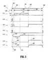
- FIG. 2shows a timing diagram representing operation of the V t compensation AMOLED pixel circuit of FIG. 1 ;
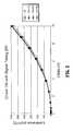
- FIG. 3shows an OLED luminance transfer function with input data voltage (V data ) and initial threshold voltage (V ti ), and with V ti increased by 1V, 2V and 5V, according to an embodiment of the present invention
- FIG. 4shows the percent luminance loss as a function of V data as V ti is increased by 1V, 2V and 5 V.
- FIG. 1shows an AMOLED pixel circuit suitable for fast threshold voltage (V t ) compensation without switching of the cathode voltage.
- the AMOLED pixel circuit 100has four signal inputs 101 , 102 , 108 and 109 ; specifically, a data signal input 101 for carrying a column signal presenting analog voltage data i.e., converted image data, a gate signal input 102 for carrying a row addressing logic signal for writing data, an on/off signal input 108 for carrying a logic signal for allowing or preventing current flow by, for example, turning a thin-film transistor (TFT) on or off, and a reverse bias voltage signal input 109 for carrying a logic signal for establishing a reverse bias voltage.
- TFTthin-film transistor
- Data signal input 101 and gate signal input 102are common column and row active matrix display pixel addressing signal inputs known to those of ordinary skill in the art for writing data or an image to a display.
- the gate lines (rows)are sequentially addressed, typically from the top to the bottom of the display, while data for each row is presented on the data lines (columns).
- the on/off signal input 108 and reverse bias voltage signal input 109are non-addessing signal inputs since these signals are not directly involved with writing data to the pixels in the display.
- Circuit 100has three power supply connections or steady voltage connections, including a positive supply voltage connection 110 , a negative supply voltage connection 111 and a reverse bias voltage connection 112 .
- Circuit 100also includes an OLED 106 , a storage capacitor 107 , and TFTs 103 , 104 and 105 .
- the OLEDis made from organic material, including, for example, an electron transport and emitting layer made from tris(8-hydroxyquinolinato)aluminim (Alq 3 ), and a hole transport layer made from N,N′-di(naphthalene-1-y-1)-N,N′diphenyl-benzidine (NPB).
- TFTs 103 , 104 and 105are made from, for example, amorphous silicon (a-Si).
- the storage capacitor 107represents the parallel combination of a gate to source capacitor of TFT 104 and any additional storage capacitors in the circuit.
- a “storage capacitor”encompasses the gate to source capacitor of TFT 104 and any additional storage capacitors in the circuit that are in combination with the gate to source capacitor of TFT 104 .
- a capacitance or a voltage on or across the storage capacitormeans a capacitance or voltage on or across the gate to source capacitor of TFT 104 and any additional storage capacitors in the circuit that are in combination with the gate to source capacitor of TFT 104 .
- the OLED 106has an anode connected to circuit node 114 and a cathode connected to the negative power supply connection 111 .
- TFT 103 and TFT 105are bottom gate fabricated TFTs, including only bottom gates. The bottom gate of TFT 103 is connected to gate input 102 . Data input 101 is connected to a drain/source contact of TFT 103 . The bottom gate of TFT 105 is connected to the reverse bias voltage signal input 109 .
- TFT 104is fabricated with both a bottom gate and a top gate. The bottom gate of TFT 104 is connected to circuit node 113 and the top gate of TFT 104 is connected to the on/off signal input 108 .
- the top gate of TFT 104operates as a depletion gate, stopping drain to source current with a logic low input signal (e.g. “0”) from the on/off signal input 108 .
- a logic high input signal (e.g. “1”) from the on/off signal input 108allows drain to source current to flow as determined by the bottom gate to source voltage.
- the positive supply voltage(i.e., the voltage at the positive supply voltage connection 110 ) is greater (more positive) than or equal to the maximum data voltage on data signal input 101 plus the maximum voltage on OLED 106 and the voltage at the negative supply terminal 111 .
- the positive supply voltageis greater than or equal to the negative of the minimum V t of TFT 104 and the negative of the illumination onset voltage of OLED 106 .
- the reverse bias voltage(i.e., the voltage at the reverse bias voltage connection 112 ) is less than the negative of the maximum V t of TFT 104 , for example, ⁇ 8V. Therefore, the reverse bias voltage may be approximately ⁇ 12V or less.
- the minimum voltage on data signal input 101is 0V or ground.
- the maximum voltage on data signal input 101corresponds to the maximum luminance for OLED 106 , while the minimum voltage on data signal input 101 corresponds to zero luminance for OLED 106 .
- FIG. 2shows a signal timing diagram 200 representing operation of the pixel circuit 100 for faster V t compensation.
- Frame time period 201is divided into write V t time period 202 , write data time period 203 and expose time period 204 .
- the frame time period 201is the time between time 205 and time 208 .
- the write V t time period 202is the time between time 205 and time 206 .
- the write data time period 203is the time between time 206 and time 207 .
- the expose time period 204is the time between time 207 and time 208 .
- a second frame time periodstarts at the end of a first frame time period.
- frame time period 201may be approximately 16.7 milliseconds.
- the write data period 203 and the expose time period 204each may be approximately 8.3 milliseconds. While dependent upon TFT mobility, TFT channel width to length ratios, data storage capacitance, circuit voltages and desired accuracy, the write V t period 202 may be approximately 0.1 to 0.2 milliseconds.
- Data signal 211corresponds to the signal on data signal input 101 in circuit 100 .
- Gate signal 212is the signal on gate signal input 102 in circuit 100 .
- the signal on the on/off signal input 108is represented by on/off signal 213 .
- the signal on reverse bias voltage signal input 109is depicted as the reverse bias signal 214 .
- the voltage across storage capacitor 107is shown as the capacitor voltage 215 .
- the anode to cathode voltage across OLED 106is depicted as OLED voltage 216 .
- the luminance of OLED 106is shown by OLED luminance 217 .
- gate signal 212 and reverse biase signal 214are set to the logic high state (“1”) and the data signal 211 on data signal input 101 is 0V.
- the high logic state of gate signal 212turns TFT 103 on, thereby connecting the data signal 211 with circuit node 113 .
- the high logic state of reverse bias signal 214turns TFT 105 on, thereby connecting circuit node 114 to the reverse bias voltage terminal 112 .
- This operationreverse biases the OLED 106 to voltage 218 and sets the voltage on storage capacitor 107 to a voltage greater than or equal to the maximum V t of TFT 104 , shown as voltage 219 .
- OLED 106is generating zero luminance, which is shown as luminance 220 . The time required for this operation may be approximately 10 microseconds.
- gate signal 212 and reverse bias signal 214are set to the logic low state (“0”), thereby turning off TFT 103 and TFT 105 .
- on/off signal 213is set to the logic high state (“1”). The high logic state of on/off signal 213 allows TFT 104 to conduct a current.
- the voltage across storage capacitor 107i.e., capacitor voltage signal 215 , discharges to voltage 221 and the voltage across OLED 106 increases to voltage 222 .
- the voltage across storage capacitor 107discharges, as allowed by the remaining time in the write V t time period 202 , to a point so as to leave excess voltage on the capacitor 107 to compensate for turnoff of TFT 103 .
- voltage 221is equal to V t plus the TFT 103 turnoff correction voltage. Accordingly, the write V t time period is much less than if the voltage of the storage capacitor 107 discharged to V t without compensating for turnoff of TFT 103 .
- on/off signal 213is set to the low logic state. Voltage 222 is less than the illumination onset voltage of OLED 106 .
- gate signal 212is set to the logic high state and data signal 211 has voltage 223 . Voltage 223 is written onto circuit node 113 . Since capacitance of OLED 106 is much larger than the capacitance of storage capacitor 107 and TFT 104 is not allowed to conduct a current due to the logic low state of on/off signal 213 , voltage 222 does not change significantly.
- gate signal 212is set the logic low state, leaving voltage 223 on circuit node 113 .
- the voltage across storage capacitor 107i.e., voltage 224 , is voltage 223 plus V t .
- on/off signal 213is set the logic high state, allowing TFT 104 to conduct a current.
- TFT 104operates in saturation. Accordingly, the current through TFT 104 is proportional to the square of voltage 223 .
- the current through TFT 104increases the voltage across OLED 106 to voltage 225 and the current through TFT 104 flows into and through OLED 106 to produce luminance 226 . Since the luminance of OLED 106 is proportional to the current flowing through OLED 106 , the luminance of OLED 106 is also proportional the square of voltage 223 .
- FIG. 3shows the data voltage (V data ) to luminance transfer function of circuit 100 having signal timing 200 for TFT 104 having an initial threshold voltage (V ti ), and V ti increased by 1, 2 and 5V (V ti +1V, V ti +2V ti and V ti +5V).
- V tiinitial threshold voltage
- V tiinitial threshold voltage
- V tiincreased by 1, 2 and 5V
- Simulationsshow that voltages 221 and 222 are established in much shorter time than with conventional designs due to: 1) a much larger drain to source voltage across TFT 104 than with previous implementations; and 2) providing a correction voltage when TFT 103 is turned off.
- the V tis established on storage capacitor 107 in ⁇ 150 microseconds, which is much faster than the ⁇ 1 millisecond previously achieved with prior designs.
- the drain to source voltage across a TFTwould be equal the voltage across a storage capacitor.
- the drain to source voltage of TFT 104is, for example, 13V higher than the voltage across the storage capacitor 107 .
- the drain to source current through TFT 104 in circuit 100will be higher.
- the increase in drain to source current through the TFT 104is due to channel length modulation with voltage, whereby an increase in the drain to source voltage results in a shorter channel length and, accordingly, an increased drain to source current.
- the voltage on the storage capacitorwas increased due to a decrease in the cathode voltage at the beginning of an expose time period and stray capacitance on a circuit node.
- the change in cathode voltageoccurred to compensate for turnoff of the gate to source voltage coupling a TFT when data was written onto the storage capacitor.
- an excess voltage on capacitor 107compensates for turnoff of TFT 103 when data is written. Accordingly, the voltage on capacitor 107 is not discharged to the same extent as in previous implementations, so as to leave the excess voltage on the capacitor 107 to compensate for turnoff of TFT 103 . Therefore, there is no change in cathode voltage to compensate for TFT turnoff.
- the excess voltage left on storage capacitor 107corrects for turnoff of TFT 103 .
- the time between times 209 and 206is decreased to allow for this correction.
- circuit 100 operated in accordance with signal timing diagram 200does not switch voltages on the negative power supply connection 111 , the cathode connection to OLED 106 , or on positive power supply connection 110 to establish the V t on storage capacitor 107 .
- the on/off signal input 108 and the reverse bias signal input 109may be common to all pixels in the display. Since the voltage terminals 110 , 111 , and 112 do not switch or change voltage levels and the additional control inputs 108 and 109 are common, the display system structure may be much simpler than previous implementations.
Landscapes
- Engineering & Computer Science (AREA)
- Physics & Mathematics (AREA)
- Computer Hardware Design (AREA)
- General Physics & Mathematics (AREA)
- Theoretical Computer Science (AREA)
- Control Of Indicators Other Than Cathode Ray Tubes (AREA)
Abstract
Description
Claims (37)
Priority Applications (1)
| Application Number | Priority Date | Filing Date | Title |
|---|---|---|---|
| US10/672,373US7038392B2 (en) | 2003-09-26 | 2003-09-26 | Active-matrix light emitting display and method for obtaining threshold voltage compensation for same |
Applications Claiming Priority (1)
| Application Number | Priority Date | Filing Date | Title |
|---|---|---|---|
| US10/672,373US7038392B2 (en) | 2003-09-26 | 2003-09-26 | Active-matrix light emitting display and method for obtaining threshold voltage compensation for same |
Publications (2)
| Publication Number | Publication Date |
|---|---|
| US20050067970A1 US20050067970A1 (en) | 2005-03-31 |
| US7038392B2true US7038392B2 (en) | 2006-05-02 |
Family
ID=34376342
Family Applications (1)
| Application Number | Title | Priority Date | Filing Date |
|---|---|---|---|
| US10/672,373Expired - LifetimeUS7038392B2 (en) | 2003-09-26 | 2003-09-26 | Active-matrix light emitting display and method for obtaining threshold voltage compensation for same |
Country Status (1)
| Country | Link |
|---|---|
| US (1) | US7038392B2 (en) |
Cited By (88)
| Publication number | Priority date | Publication date | Assignee | Title |
|---|---|---|---|---|
| US20050179625A1 (en)* | 2004-01-02 | 2005-08-18 | Choi Joon-Hoo | Display device and driving method thereof |
| US20050219172A1 (en)* | 2004-03-30 | 2005-10-06 | Li-Wei Shih | Display array and display panel utilizing the same |
| US20060007070A1 (en)* | 2004-06-02 | 2006-01-12 | Li-Wei Shih | Driving circuit and driving method for electroluminescent display |
| US20060125408A1 (en)* | 2004-11-16 | 2006-06-15 | Arokia Nathan | System and driving method for active matrix light emitting device display |
| US20060138600A1 (en)* | 2004-12-28 | 2006-06-29 | Seiko Epson Corporation | Unit circuit, method of controlling unit circuit, electronic device, and electronic apparatus |
| US20060290614A1 (en)* | 2005-06-08 | 2006-12-28 | Arokia Nathan | Method and system for driving a light emitting device display |
| US7259521B1 (en)* | 2006-08-28 | 2007-08-21 | Micrel, Inc. | Video driver architecture for AMOLED displays |
| US20090244046A1 (en)* | 2008-03-26 | 2009-10-01 | Fujifilm Corporation | Pixel circuit, display apparatus, and pixel circuit drive control method |
| US20100033469A1 (en)* | 2004-12-15 | 2010-02-11 | Ignis Innovation Inc. | Method and system for programming, calibrating and driving a light emitting device display |
| US20100039458A1 (en)* | 2008-04-18 | 2010-02-18 | Ignis Innovation Inc. | System and driving method for light emitting device display |
| CN101859537A (en)* | 2009-04-01 | 2010-10-13 | 索尼公司 | Method of driving display element and method of driving display device |
| US20120062620A1 (en)* | 2007-02-21 | 2012-03-15 | Sony Corporation | Display apparatus and drive method therefor, and electronic equipment |
| US8502757B2 (en) | 2011-03-17 | 2013-08-06 | Au Optronics Corp. | Organic light emitting display having threshold voltage compensation mechanism and driving method thereof |
| US8564513B2 (en) | 2006-01-09 | 2013-10-22 | Ignis Innovation, Inc. | Method and system for driving an active matrix display circuit |
| US8599191B2 (en) | 2011-05-20 | 2013-12-03 | Ignis Innovation Inc. | System and methods for extraction of threshold and mobility parameters in AMOLED displays |
| US8723843B2 (en) | 2010-06-10 | 2014-05-13 | E Ink Holdings Inc. | Pixel driving circuit with capacitor having threshold voltages information storing function, pixel driving method and light emitting display device |
| US8743096B2 (en) | 2006-04-19 | 2014-06-03 | Ignis Innovation, Inc. | Stable driving scheme for active matrix displays |
| US8803417B2 (en) | 2009-12-01 | 2014-08-12 | Ignis Innovation Inc. | High resolution pixel architecture |
| US8907991B2 (en) | 2010-12-02 | 2014-12-09 | Ignis Innovation Inc. | System and methods for thermal compensation in AMOLED displays |
| USRE45291E1 (en) | 2004-06-29 | 2014-12-16 | Ignis Innovation Inc. | Voltage-programming scheme for current-driven AMOLED displays |
| US8922544B2 (en) | 2012-05-23 | 2014-12-30 | Ignis Innovation Inc. | Display systems with compensation for line propagation delay |
| US8941697B2 (en) | 2003-09-23 | 2015-01-27 | Ignis Innovation Inc. | Circuit and method for driving an array of light emitting pixels |
| US8994617B2 (en) | 2010-03-17 | 2015-03-31 | Ignis Innovation Inc. | Lifetime uniformity parameter extraction methods |
| US9030506B2 (en) | 2009-11-12 | 2015-05-12 | Ignis Innovation Inc. | Stable fast programming scheme for displays |
| US9093028B2 (en) | 2009-12-06 | 2015-07-28 | Ignis Innovation Inc. | System and methods for power conservation for AMOLED pixel drivers |
| US9093029B2 (en) | 2011-05-20 | 2015-07-28 | Ignis Innovation Inc. | System and methods for extraction of threshold and mobility parameters in AMOLED displays |
| US9111485B2 (en) | 2009-06-16 | 2015-08-18 | Ignis Innovation Inc. | Compensation technique for color shift in displays |
| US9125278B2 (en) | 2006-08-15 | 2015-09-01 | Ignis Innovation Inc. | OLED luminance degradation compensation |
| US9153172B2 (en) | 2004-12-07 | 2015-10-06 | Ignis Innovation Inc. | Method and system for programming and driving active matrix light emitting device pixel having a controllable supply voltage |
| US9171500B2 (en) | 2011-05-20 | 2015-10-27 | Ignis Innovation Inc. | System and methods for extraction of parasitic parameters in AMOLED displays |
| US9171504B2 (en) | 2013-01-14 | 2015-10-27 | Ignis Innovation Inc. | Driving scheme for emissive displays providing compensation for driving transistor variations |
| US9269322B2 (en) | 2006-01-09 | 2016-02-23 | Ignis Innovation Inc. | Method and system for driving an active matrix display circuit |
| US9275579B2 (en) | 2004-12-15 | 2016-03-01 | Ignis Innovation Inc. | System and methods for extraction of threshold and mobility parameters in AMOLED displays |
| US9280933B2 (en) | 2004-12-15 | 2016-03-08 | Ignis Innovation Inc. | System and methods for extraction of threshold and mobility parameters in AMOLED displays |
| US9305488B2 (en) | 2013-03-14 | 2016-04-05 | Ignis Innovation Inc. | Re-interpolation with edge detection for extracting an aging pattern for AMOLED displays |
| US9311859B2 (en) | 2009-11-30 | 2016-04-12 | Ignis Innovation Inc. | Resetting cycle for aging compensation in AMOLED displays |
| US9324268B2 (en) | 2013-03-15 | 2016-04-26 | Ignis Innovation Inc. | Amoled displays with multiple readout circuits |
| US9336717B2 (en) | 2012-12-11 | 2016-05-10 | Ignis Innovation Inc. | Pixel circuits for AMOLED displays |
| US9343006B2 (en) | 2012-02-03 | 2016-05-17 | Ignis Innovation Inc. | Driving system for active-matrix displays |
| US9351368B2 (en) | 2013-03-08 | 2016-05-24 | Ignis Innovation Inc. | Pixel circuits for AMOLED displays |
| US9370075B2 (en) | 2008-12-09 | 2016-06-14 | Ignis Innovation Inc. | System and method for fast compensation programming of pixels in a display |
| US9384698B2 (en) | 2009-11-30 | 2016-07-05 | Ignis Innovation Inc. | System and methods for aging compensation in AMOLED displays |
| US9430958B2 (en) | 2010-02-04 | 2016-08-30 | Ignis Innovation Inc. | System and methods for extracting correlation curves for an organic light emitting device |
| US9437137B2 (en) | 2013-08-12 | 2016-09-06 | Ignis Innovation Inc. | Compensation accuracy |
| US9466240B2 (en) | 2011-05-26 | 2016-10-11 | Ignis Innovation Inc. | Adaptive feedback system for compensating for aging pixel areas with enhanced estimation speed |
| US9489891B2 (en) | 2006-01-09 | 2016-11-08 | Ignis Innovation Inc. | Method and system for driving an active matrix display circuit |
| US9530349B2 (en) | 2011-05-20 | 2016-12-27 | Ignis Innovations Inc. | Charged-based compensation and parameter extraction in AMOLED displays |
| US9697771B2 (en) | 2013-03-08 | 2017-07-04 | Ignis Innovation Inc. | Pixel circuits for AMOLED displays |
| US9721505B2 (en) | 2013-03-08 | 2017-08-01 | Ignis Innovation Inc. | Pixel circuits for AMOLED displays |
| WO2017128468A1 (en)* | 2016-01-29 | 2017-08-03 | 深圳市华星光电技术有限公司 | Pixel compensation circuit, method, and flat display device |
| US9741282B2 (en) | 2013-12-06 | 2017-08-22 | Ignis Innovation Inc. | OLED display system and method |
| US9747834B2 (en) | 2012-05-11 | 2017-08-29 | Ignis Innovation Inc. | Pixel circuits including feedback capacitors and reset capacitors, and display systems therefore |
| US9761170B2 (en) | 2013-12-06 | 2017-09-12 | Ignis Innovation Inc. | Correction for localized phenomena in an image array |
| US9773439B2 (en) | 2011-05-27 | 2017-09-26 | Ignis Innovation Inc. | Systems and methods for aging compensation in AMOLED displays |
| USRE46561E1 (en) | 2008-07-29 | 2017-09-26 | Ignis Innovation Inc. | Method and system for driving light emitting display |
| US9786223B2 (en) | 2012-12-11 | 2017-10-10 | Ignis Innovation Inc. | Pixel circuits for AMOLED displays |
| US9786209B2 (en) | 2009-11-30 | 2017-10-10 | Ignis Innovation Inc. | System and methods for aging compensation in AMOLED displays |
| US9799246B2 (en) | 2011-05-20 | 2017-10-24 | Ignis Innovation Inc. | System and methods for extraction of threshold and mobility parameters in AMOLED displays |
| US9830857B2 (en) | 2013-01-14 | 2017-11-28 | Ignis Innovation Inc. | Cleaning common unwanted signals from pixel measurements in emissive displays |
| US9881532B2 (en) | 2010-02-04 | 2018-01-30 | Ignis Innovation Inc. | System and method for extracting correlation curves for an organic light emitting device |
| US9881587B2 (en) | 2011-05-28 | 2018-01-30 | Ignis Innovation Inc. | Systems and methods for operating pixels in a display to mitigate image flicker |
| US9886899B2 (en) | 2011-05-17 | 2018-02-06 | Ignis Innovation Inc. | Pixel Circuits for AMOLED displays |
| US9947293B2 (en) | 2015-05-27 | 2018-04-17 | Ignis Innovation Inc. | Systems and methods of reduced memory bandwidth compensation |
| US10013907B2 (en) | 2004-12-15 | 2018-07-03 | Ignis Innovation Inc. | Method and system for programming, calibrating and/or compensating, and driving an LED display |
| US10012678B2 (en) | 2004-12-15 | 2018-07-03 | Ignis Innovation Inc. | Method and system for programming, calibrating and/or compensating, and driving an LED display |
| US10019941B2 (en) | 2005-09-13 | 2018-07-10 | Ignis Innovation Inc. | Compensation technique for luminance degradation in electro-luminance devices |
| US10074304B2 (en) | 2015-08-07 | 2018-09-11 | Ignis Innovation Inc. | Systems and methods of pixel calibration based on improved reference values |
| US10078984B2 (en) | 2005-02-10 | 2018-09-18 | Ignis Innovation Inc. | Driving circuit for current programmed organic light-emitting diode displays |
| US10089924B2 (en) | 2011-11-29 | 2018-10-02 | Ignis Innovation Inc. | Structural and low-frequency non-uniformity compensation |
| US10089921B2 (en) | 2010-02-04 | 2018-10-02 | Ignis Innovation Inc. | System and methods for extracting correlation curves for an organic light emitting device |
| US10102808B2 (en) | 2015-10-14 | 2018-10-16 | Ignis Innovation Inc. | Systems and methods of multiple color driving |
| US10134325B2 (en) | 2014-12-08 | 2018-11-20 | Ignis Innovation Inc. | Integrated display system |
| US10152915B2 (en) | 2015-04-01 | 2018-12-11 | Ignis Innovation Inc. | Systems and methods of display brightness adjustment |
| US10163401B2 (en) | 2010-02-04 | 2018-12-25 | Ignis Innovation Inc. | System and methods for extracting correlation curves for an organic light emitting device |
| US10176736B2 (en) | 2010-02-04 | 2019-01-08 | Ignis Innovation Inc. | System and methods for extracting correlation curves for an organic light emitting device |
| US10181282B2 (en) | 2015-01-23 | 2019-01-15 | Ignis Innovation Inc. | Compensation for color variations in emissive devices |
| US10192479B2 (en) | 2014-04-08 | 2019-01-29 | Ignis Innovation Inc. | Display system using system level resources to calculate compensation parameters for a display module in a portable device |
| US10235933B2 (en) | 2005-04-12 | 2019-03-19 | Ignis Innovation Inc. | System and method for compensation of non-uniformities in light emitting device displays |
| US10242619B2 (en) | 2013-03-08 | 2019-03-26 | Ignis Innovation Inc. | Pixel circuits for amoled displays |
| US10311780B2 (en) | 2015-05-04 | 2019-06-04 | Ignis Innovation Inc. | Systems and methods of optical feedback |
| US10319307B2 (en) | 2009-06-16 | 2019-06-11 | Ignis Innovation Inc. | Display system with compensation techniques and/or shared level resources |
| US10373554B2 (en) | 2015-07-24 | 2019-08-06 | Ignis Innovation Inc. | Pixels and reference circuits and timing techniques |
| US10410579B2 (en) | 2015-07-24 | 2019-09-10 | Ignis Innovation Inc. | Systems and methods of hybrid calibration of bias current |
| US10439159B2 (en) | 2013-12-25 | 2019-10-08 | Ignis Innovation Inc. | Electrode contacts |
| US10573231B2 (en) | 2010-02-04 | 2020-02-25 | Ignis Innovation Inc. | System and methods for extracting correlation curves for an organic light emitting device |
| US10657895B2 (en) | 2015-07-24 | 2020-05-19 | Ignis Innovation Inc. | Pixels and reference circuits and timing techniques |
| US10867536B2 (en) | 2013-04-22 | 2020-12-15 | Ignis Innovation Inc. | Inspection system for OLED display panels |
| US10996258B2 (en) | 2009-11-30 | 2021-05-04 | Ignis Innovation Inc. | Defect detection and correction of pixel circuits for AMOLED displays |
Families Citing this family (37)
| Publication number | Priority date | Publication date | Assignee | Title |
|---|---|---|---|---|
| US7569849B2 (en)* | 2001-02-16 | 2009-08-04 | Ignis Innovation Inc. | Pixel driver circuit and pixel circuit having the pixel driver circuit |
| CA2419704A1 (en) | 2003-02-24 | 2004-08-24 | Ignis Innovation Inc. | Method of manufacturing a pixel with organic light-emitting diode |
| DE102004002587B4 (en)* | 2004-01-16 | 2006-06-01 | Novaled Gmbh | Image element for an active matrix display |
| CA2495726A1 (en) | 2005-01-28 | 2006-07-28 | Ignis Innovation Inc. | Locally referenced voltage programmed pixel for amoled displays |
| TWI330726B (en)* | 2005-09-05 | 2010-09-21 | Au Optronics Corp | Display apparatus, thin-film-transistor discharge method and electrical driving method therefor |
| US8004477B2 (en)* | 2005-11-14 | 2011-08-23 | Sony Corporation | Display apparatus and driving method thereof |
| EP1793366A3 (en) | 2005-12-02 | 2009-11-04 | Semiconductor Energy Laboratory Co., Ltd. | Semiconductor device, display device, and electronic device |
| JP4240059B2 (en)* | 2006-05-22 | 2009-03-18 | ソニー株式会社 | Display device and driving method thereof |
| TWI348677B (en)* | 2006-09-12 | 2011-09-11 | Ind Tech Res Inst | System for increasing circuit reliability and method thereof |
| JP5194781B2 (en)* | 2007-12-26 | 2013-05-08 | ソニー株式会社 | Display device, driving method thereof, and electronic apparatus |
| US8358258B1 (en)* | 2008-03-16 | 2013-01-22 | Nongqiang Fan | Active matrix display having pixel element with light-emitting element |
| CA2631683A1 (en)* | 2008-04-16 | 2009-10-16 | Ignis Innovation Inc. | Recovery of temporal non-uniformities in active matrix displays |
| KR101101070B1 (en)* | 2009-10-12 | 2011-12-30 | 삼성모바일디스플레이주식회사 | Organic light emitting display |
| JP2011141418A (en)* | 2010-01-07 | 2011-07-21 | Sony Corp | Display apparatus, light detection method and electronic apparatus |
| US9606607B2 (en) | 2011-05-17 | 2017-03-28 | Ignis Innovation Inc. | Systems and methods for display systems with dynamic power control |
| CN109272933A (en) | 2011-05-17 | 2019-01-25 | 伊格尼斯创新公司 | The method for operating display |
| TWI444972B (en) | 2011-07-29 | 2014-07-11 | Innolux Corp | Display system |
| US9070775B2 (en) | 2011-08-03 | 2015-06-30 | Ignis Innovations Inc. | Thin film transistor |
| US8901579B2 (en) | 2011-08-03 | 2014-12-02 | Ignis Innovation Inc. | Organic light emitting diode and method of manufacturing |
| US9385169B2 (en) | 2011-11-29 | 2016-07-05 | Ignis Innovation Inc. | Multi-functional active matrix organic light-emitting diode display |
| US20140002332A1 (en)* | 2012-06-29 | 2014-01-02 | Taiwan Semiconductor Manufacturing Company, Ltd. | Pixels for display |
| US9952698B2 (en) | 2013-03-15 | 2018-04-24 | Ignis Innovation Inc. | Dynamic adjustment of touch resolutions on an AMOLED display |
| US10997901B2 (en) | 2014-02-28 | 2021-05-04 | Ignis Innovation Inc. | Display system |
| US10176752B2 (en) | 2014-03-24 | 2019-01-08 | Ignis Innovation Inc. | Integrated gate driver |
| CA2872563A1 (en) | 2014-11-28 | 2016-05-28 | Ignis Innovation Inc. | High pixel density array architecture |
| CN104732929A (en)* | 2015-04-16 | 2015-06-24 | 京东方科技集团股份有限公司 | Pixel circuit and driving method thereof and display device |
| CA2909813A1 (en) | 2015-10-26 | 2017-04-26 | Ignis Innovation Inc | High ppi pattern orientation |
| EP3523832B1 (en)* | 2016-10-04 | 2020-05-13 | Koninklijke Philips N.V. | Actuator device based on an electroactive polymer |
| CN106504699B (en)* | 2016-10-14 | 2019-02-01 | 深圳市华星光电技术有限公司 | AMOLED pixel-driving circuit and driving method |
| US10431142B2 (en)* | 2016-11-14 | 2019-10-01 | Int Tech Co., Ltd. | Pixel circuit and electroluminescent display comprising the pixel circuit |
| US10586491B2 (en) | 2016-12-06 | 2020-03-10 | Ignis Innovation Inc. | Pixel circuits for mitigation of hysteresis |
| CN108305587A (en)* | 2017-01-11 | 2018-07-20 | 群创光电股份有限公司 | Display device |
| US10714018B2 (en) | 2017-05-17 | 2020-07-14 | Ignis Innovation Inc. | System and method for loading image correction data for displays |
| CN107170413B (en) | 2017-07-26 | 2019-01-18 | 江苏集萃有机光电技术研究所有限公司 | The driving method of pixel circuit and pixel circuit |
| US11025899B2 (en) | 2017-08-11 | 2021-06-01 | Ignis Innovation Inc. | Optical correction systems and methods for correcting non-uniformity of emissive display devices |
| US10971078B2 (en) | 2018-02-12 | 2021-04-06 | Ignis Innovation Inc. | Pixel measurement through data line |
| CN110189691B (en)* | 2019-05-14 | 2021-03-16 | 深圳市华星光电半导体显示技术有限公司 | Pixel driving circuit and display panel |
Citations (4)
| Publication number | Priority date | Publication date | Assignee | Title |
|---|---|---|---|---|
| US6229506B1 (en) | 1997-04-23 | 2001-05-08 | Sarnoff Corporation | Active matrix light emitting diode pixel structure and concomitant method |
| US6229508B1 (en) | 1997-09-29 | 2001-05-08 | Sarnoff Corporation | Active matrix light emitting diode pixel structure and concomitant method |
| US6348906B1 (en)* | 1998-09-03 | 2002-02-19 | Sarnoff Corporation | Line scanning circuit for a dual-mode display |
| US6359605B1 (en)* | 1998-06-12 | 2002-03-19 | U.S. Philips Corporation | Active matrix electroluminescent display devices |
- 2003
- 2003-09-26USUS10/672,373patent/US7038392B2/ennot_activeExpired - Lifetime
Patent Citations (4)
| Publication number | Priority date | Publication date | Assignee | Title |
|---|---|---|---|---|
| US6229506B1 (en) | 1997-04-23 | 2001-05-08 | Sarnoff Corporation | Active matrix light emitting diode pixel structure and concomitant method |
| US6229508B1 (en) | 1997-09-29 | 2001-05-08 | Sarnoff Corporation | Active matrix light emitting diode pixel structure and concomitant method |
| US6359605B1 (en)* | 1998-06-12 | 2002-03-19 | U.S. Philips Corporation | Active matrix electroluminescent display devices |
| US6348906B1 (en)* | 1998-09-03 | 2002-02-19 | Sarnoff Corporation | Line scanning circuit for a dual-mode display |
Non-Patent Citations (6)
| Title |
|---|
| Dawson, R.M.A., et al., A Poly-Si Active-Matrix OLED Display with Integrated Drivers, SID 98 Digest, pp. 438-441. |
| Dawson, R.M.A., et al., Design of an Improved Pixel for a Polysilicon Active-Matrix Organic LED Display, SID 98 Digest, pp. 11-14. |
| Dawson, R.M.A., et al., The Impact of the Transient Response of Organic Light Emitting Diodes on the Design of Active Matrix OLED Displays, International Electron Devices Meeting, Dec. 6-9, 1998, San Francisco, CA. |
| Hattori, Reiji, et al., Current-Writing Active-Matrix Circuit for Organic Light-Emitting Diode Display Using a-Si:H Thin-Film-Transistors, IEICE Trans. Electron., vol. E83-C, No. 5, May 2000, pp. 779-782. |
| He, Yi, et al., Electrical Reliability of Two- and Four-a-Si:H TFT Pixel Electrode Circuits for Active-Matrix OLEDs, SID 2000 Digest, pp. 354-357. |
| Wu, Biing-Seng, et al., A Novel Depletion-Gate Amorphous Silicon Thin-Film Transistor, IEEE Electron Device Letters, vol. 13, No. 1, Jan. 1992, pp. 17-19. |
Cited By (203)
| Publication number | Priority date | Publication date | Assignee | Title |
|---|---|---|---|---|
| US10089929B2 (en) | 2003-09-23 | 2018-10-02 | Ignis Innovation Inc. | Pixel driver circuit with load-balance in current mirror circuit |
| US8941697B2 (en) | 2003-09-23 | 2015-01-27 | Ignis Innovation Inc. | Circuit and method for driving an array of light emitting pixels |
| US9472139B2 (en) | 2003-09-23 | 2016-10-18 | Ignis Innovation Inc. | Circuit and method for driving an array of light emitting pixels |
| US9472138B2 (en) | 2003-09-23 | 2016-10-18 | Ignis Innovation Inc. | Pixel driver circuit with load-balance in current mirror circuit |
| US9852689B2 (en) | 2003-09-23 | 2017-12-26 | Ignis Innovation Inc. | Circuit and method for driving an array of light emitting pixels |
| US7859494B2 (en)* | 2004-01-02 | 2010-12-28 | Samsung Electronics Co., Ltd. | Display device and driving method thereof |
| US20050179625A1 (en)* | 2004-01-02 | 2005-08-18 | Choi Joon-Hoo | Display device and driving method thereof |
| US20050219172A1 (en)* | 2004-03-30 | 2005-10-06 | Li-Wei Shih | Display array and display panel utilizing the same |
| US8253664B2 (en)* | 2004-03-30 | 2012-08-28 | Au Optronics Corp. | Display array with a plurality of display units corresponding to one set of the data and scan lines and each comprising a control unit |
| US20060007070A1 (en)* | 2004-06-02 | 2006-01-12 | Li-Wei Shih | Driving circuit and driving method for electroluminescent display |
| USRE45291E1 (en) | 2004-06-29 | 2014-12-16 | Ignis Innovation Inc. | Voltage-programming scheme for current-driven AMOLED displays |
| USRE47257E1 (en) | 2004-06-29 | 2019-02-26 | Ignis Innovation Inc. | Voltage-programming scheme for current-driven AMOLED displays |
| US20060125408A1 (en)* | 2004-11-16 | 2006-06-15 | Arokia Nathan | System and driving method for active matrix light emitting device display |
| US8319712B2 (en) | 2004-11-16 | 2012-11-27 | Ignis Innovation Inc. | System and driving method for active matrix light emitting device display |
| US7889159B2 (en) | 2004-11-16 | 2011-02-15 | Ignis Innovation Inc. | System and driving method for active matrix light emitting device display |
| US20110134094A1 (en)* | 2004-11-16 | 2011-06-09 | Ignis Innovation Inc. | System and driving method for active matrix light emitting device display |
| US9153172B2 (en) | 2004-12-07 | 2015-10-06 | Ignis Innovation Inc. | Method and system for programming and driving active matrix light emitting device pixel having a controllable supply voltage |
| US9741292B2 (en) | 2004-12-07 | 2017-08-22 | Ignis Innovation Inc. | Method and system for programming and driving active matrix light emitting device pixel having a controllable supply voltage |
| US10012678B2 (en) | 2004-12-15 | 2018-07-03 | Ignis Innovation Inc. | Method and system for programming, calibrating and/or compensating, and driving an LED display |
| US9280933B2 (en) | 2004-12-15 | 2016-03-08 | Ignis Innovation Inc. | System and methods for extraction of threshold and mobility parameters in AMOLED displays |
| US10699624B2 (en) | 2004-12-15 | 2020-06-30 | Ignis Innovation Inc. | Method and system for programming, calibrating and/or compensating, and driving an LED display |
| US9275579B2 (en) | 2004-12-15 | 2016-03-01 | Ignis Innovation Inc. | System and methods for extraction of threshold and mobility parameters in AMOLED displays |
| US10013907B2 (en) | 2004-12-15 | 2018-07-03 | Ignis Innovation Inc. | Method and system for programming, calibrating and/or compensating, and driving an LED display |
| US8736524B2 (en) | 2004-12-15 | 2014-05-27 | Ignis Innovation, Inc. | Method and system for programming, calibrating and driving a light emitting device display |
| US8259044B2 (en) | 2004-12-15 | 2012-09-04 | Ignis Innovation Inc. | Method and system for programming, calibrating and driving a light emitting device display |
| US8994625B2 (en) | 2004-12-15 | 2015-03-31 | Ignis Innovation Inc. | Method and system for programming, calibrating and driving a light emitting device display |
| US20100033469A1 (en)* | 2004-12-15 | 2010-02-11 | Ignis Innovation Inc. | Method and system for programming, calibrating and driving a light emitting device display |
| US9970964B2 (en) | 2004-12-15 | 2018-05-15 | Ignis Innovation Inc. | Method and system for programming, calibrating and driving a light emitting device display |
| US8816946B2 (en) | 2004-12-15 | 2014-08-26 | Ignis Innovation Inc. | Method and system for programming, calibrating and driving a light emitting device display |
| US7259593B2 (en)* | 2004-12-28 | 2007-08-21 | Seiko Epson Corporation | Unit circuit, method of controlling unit circuit, electronic device, and electronic apparatus |
| US20060138600A1 (en)* | 2004-12-28 | 2006-06-29 | Seiko Epson Corporation | Unit circuit, method of controlling unit circuit, electronic device, and electronic apparatus |
| US10078984B2 (en) | 2005-02-10 | 2018-09-18 | Ignis Innovation Inc. | Driving circuit for current programmed organic light-emitting diode displays |
| US10235933B2 (en) | 2005-04-12 | 2019-03-19 | Ignis Innovation Inc. | System and method for compensation of non-uniformities in light emitting device displays |
| US9805653B2 (en) | 2005-06-08 | 2017-10-31 | Ignis Innovation Inc. | Method and system for driving a light emitting device display |
| US8860636B2 (en) | 2005-06-08 | 2014-10-14 | Ignis Innovation Inc. | Method and system for driving a light emitting device display |
| US9330598B2 (en) | 2005-06-08 | 2016-05-03 | Ignis Innovation Inc. | Method and system for driving a light emitting device display |
| US10388221B2 (en) | 2005-06-08 | 2019-08-20 | Ignis Innovation Inc. | Method and system for driving a light emitting device display |
| US7852298B2 (en) | 2005-06-08 | 2010-12-14 | Ignis Innovation Inc. | Method and system for driving a light emitting device display |
| US20060290614A1 (en)* | 2005-06-08 | 2006-12-28 | Arokia Nathan | Method and system for driving a light emitting device display |
| US20110012884A1 (en)* | 2005-06-08 | 2011-01-20 | Ignis Innovation Inc. | Method and system for driving a light emitting device display |
| US10019941B2 (en) | 2005-09-13 | 2018-07-10 | Ignis Innovation Inc. | Compensation technique for luminance degradation in electro-luminance devices |
| US10262587B2 (en) | 2006-01-09 | 2019-04-16 | Ignis Innovation Inc. | Method and system for driving an active matrix display circuit |
| US9269322B2 (en) | 2006-01-09 | 2016-02-23 | Ignis Innovation Inc. | Method and system for driving an active matrix display circuit |
| US8564513B2 (en) | 2006-01-09 | 2013-10-22 | Ignis Innovation, Inc. | Method and system for driving an active matrix display circuit |
| US9058775B2 (en) | 2006-01-09 | 2015-06-16 | Ignis Innovation Inc. | Method and system for driving an active matrix display circuit |
| US10229647B2 (en) | 2006-01-09 | 2019-03-12 | Ignis Innovation Inc. | Method and system for driving an active matrix display circuit |
| US9489891B2 (en) | 2006-01-09 | 2016-11-08 | Ignis Innovation Inc. | Method and system for driving an active matrix display circuit |
| US8624808B2 (en) | 2006-01-09 | 2014-01-07 | Ignis Innovation Inc. | Method and system for driving an active matrix display circuit |
| US9842544B2 (en) | 2006-04-19 | 2017-12-12 | Ignis Innovation Inc. | Stable driving scheme for active matrix displays |
| US9633597B2 (en) | 2006-04-19 | 2017-04-25 | Ignis Innovation Inc. | Stable driving scheme for active matrix displays |
| US10127860B2 (en) | 2006-04-19 | 2018-11-13 | Ignis Innovation Inc. | Stable driving scheme for active matrix displays |
| US10453397B2 (en) | 2006-04-19 | 2019-10-22 | Ignis Innovation Inc. | Stable driving scheme for active matrix displays |
| US8743096B2 (en) | 2006-04-19 | 2014-06-03 | Ignis Innovation, Inc. | Stable driving scheme for active matrix displays |
| US9530352B2 (en) | 2006-08-15 | 2016-12-27 | Ignis Innovations Inc. | OLED luminance degradation compensation |
| US9125278B2 (en) | 2006-08-15 | 2015-09-01 | Ignis Innovation Inc. | OLED luminance degradation compensation |
| US10325554B2 (en) | 2006-08-15 | 2019-06-18 | Ignis Innovation Inc. | OLED luminance degradation compensation |
| US7259521B1 (en)* | 2006-08-28 | 2007-08-21 | Micrel, Inc. | Video driver architecture for AMOLED displays |
| US8890782B2 (en) | 2007-02-21 | 2014-11-18 | Sony Corporation | Display apparatus and drive method therefor, and electronic equipment |
| US20120062620A1 (en)* | 2007-02-21 | 2012-03-15 | Sony Corporation | Display apparatus and drive method therefor, and electronic equipment |
| US8537080B2 (en)* | 2007-02-21 | 2013-09-17 | Sony Corporation | Display apparatus and drive method therefor, and electronic equipment |
| US8368678B2 (en)* | 2008-03-26 | 2013-02-05 | Fujifilm Corporation | Pixel circuit, display apparatus, and pixel circuit drive control method |
| US20090244046A1 (en)* | 2008-03-26 | 2009-10-01 | Fujifilm Corporation | Pixel circuit, display apparatus, and pixel circuit drive control method |
| US20100039458A1 (en)* | 2008-04-18 | 2010-02-18 | Ignis Innovation Inc. | System and driving method for light emitting device display |
| US8614652B2 (en) | 2008-04-18 | 2013-12-24 | Ignis Innovation Inc. | System and driving method for light emitting device display |
| US9867257B2 (en) | 2008-04-18 | 2018-01-09 | Ignis Innovation Inc. | System and driving method for light emitting device display |
| US10555398B2 (en) | 2008-04-18 | 2020-02-04 | Ignis Innovation Inc. | System and driving method for light emitting device display |
| US9877371B2 (en) | 2008-04-18 | 2018-01-23 | Ignis Innovations Inc. | System and driving method for light emitting device display |
| USRE49389E1 (en) | 2008-07-29 | 2023-01-24 | Ignis Innovation Inc. | Method and system for driving light emitting display |
| USRE46561E1 (en) | 2008-07-29 | 2017-09-26 | Ignis Innovation Inc. | Method and system for driving light emitting display |
| US11030949B2 (en) | 2008-12-09 | 2021-06-08 | Ignis Innovation Inc. | Systems and method for fast compensation programming of pixels in a display |
| US10134335B2 (en) | 2008-12-09 | 2018-11-20 | Ignis Innovation Inc. | Systems and method for fast compensation programming of pixels in a display |
| US9370075B2 (en) | 2008-12-09 | 2016-06-14 | Ignis Innovation Inc. | System and method for fast compensation programming of pixels in a display |
| US9824632B2 (en) | 2008-12-09 | 2017-11-21 | Ignis Innovation Inc. | Systems and method for fast compensation programming of pixels in a display |
| CN101859537B (en)* | 2009-04-01 | 2013-02-06 | 索尼公司 | Method of driving display element and method of driving display device |
| CN101859537A (en)* | 2009-04-01 | 2010-10-13 | 索尼公司 | Method of driving display element and method of driving display device |
| US9418587B2 (en) | 2009-06-16 | 2016-08-16 | Ignis Innovation Inc. | Compensation technique for color shift in displays |
| US10553141B2 (en) | 2009-06-16 | 2020-02-04 | Ignis Innovation Inc. | Compensation technique for color shift in displays |
| US10319307B2 (en) | 2009-06-16 | 2019-06-11 | Ignis Innovation Inc. | Display system with compensation techniques and/or shared level resources |
| US9117400B2 (en) | 2009-06-16 | 2015-08-25 | Ignis Innovation Inc. | Compensation technique for color shift in displays |
| US9111485B2 (en) | 2009-06-16 | 2015-08-18 | Ignis Innovation Inc. | Compensation technique for color shift in displays |
| US9030506B2 (en) | 2009-11-12 | 2015-05-12 | Ignis Innovation Inc. | Stable fast programming scheme for displays |
| US9311859B2 (en) | 2009-11-30 | 2016-04-12 | Ignis Innovation Inc. | Resetting cycle for aging compensation in AMOLED displays |
| US10679533B2 (en) | 2009-11-30 | 2020-06-09 | Ignis Innovation Inc. | System and methods for aging compensation in AMOLED displays |
| US10304390B2 (en) | 2009-11-30 | 2019-05-28 | Ignis Innovation Inc. | System and methods for aging compensation in AMOLED displays |
| US10996258B2 (en) | 2009-11-30 | 2021-05-04 | Ignis Innovation Inc. | Defect detection and correction of pixel circuits for AMOLED displays |
| US12033589B2 (en) | 2009-11-30 | 2024-07-09 | Ignis Innovation Inc. | System and methods for aging compensation in AMOLED displays |
| US10699613B2 (en) | 2009-11-30 | 2020-06-30 | Ignis Innovation Inc. | Resetting cycle for aging compensation in AMOLED displays |
| US9786209B2 (en) | 2009-11-30 | 2017-10-10 | Ignis Innovation Inc. | System and methods for aging compensation in AMOLED displays |
| US9384698B2 (en) | 2009-11-30 | 2016-07-05 | Ignis Innovation Inc. | System and methods for aging compensation in AMOLED displays |
| US9059117B2 (en) | 2009-12-01 | 2015-06-16 | Ignis Innovation Inc. | High resolution pixel architecture |
| US8803417B2 (en) | 2009-12-01 | 2014-08-12 | Ignis Innovation Inc. | High resolution pixel architecture |
| US9262965B2 (en) | 2009-12-06 | 2016-02-16 | Ignis Innovation Inc. | System and methods for power conservation for AMOLED pixel drivers |
| US9093028B2 (en) | 2009-12-06 | 2015-07-28 | Ignis Innovation Inc. | System and methods for power conservation for AMOLED pixel drivers |
| US10176736B2 (en) | 2010-02-04 | 2019-01-08 | Ignis Innovation Inc. | System and methods for extracting correlation curves for an organic light emitting device |
| US9773441B2 (en) | 2010-02-04 | 2017-09-26 | Ignis Innovation Inc. | System and methods for extracting correlation curves for an organic light emitting device |
| US11200839B2 (en) | 2010-02-04 | 2021-12-14 | Ignis Innovation Inc. | System and methods for extracting correlation curves for an organic light emitting device |
| US10573231B2 (en) | 2010-02-04 | 2020-02-25 | Ignis Innovation Inc. | System and methods for extracting correlation curves for an organic light emitting device |
| US10089921B2 (en) | 2010-02-04 | 2018-10-02 | Ignis Innovation Inc. | System and methods for extracting correlation curves for an organic light emitting device |
| US9430958B2 (en) | 2010-02-04 | 2016-08-30 | Ignis Innovation Inc. | System and methods for extracting correlation curves for an organic light emitting device |
| US10032399B2 (en) | 2010-02-04 | 2018-07-24 | Ignis Innovation Inc. | System and methods for extracting correlation curves for an organic light emitting device |
| US10163401B2 (en) | 2010-02-04 | 2018-12-25 | Ignis Innovation Inc. | System and methods for extracting correlation curves for an organic light emitting device |
| US10971043B2 (en) | 2010-02-04 | 2021-04-06 | Ignis Innovation Inc. | System and method for extracting correlation curves for an organic light emitting device |
| US10395574B2 (en) | 2010-02-04 | 2019-08-27 | Ignis Innovation Inc. | System and methods for extracting correlation curves for an organic light emitting device |
| US9881532B2 (en) | 2010-02-04 | 2018-01-30 | Ignis Innovation Inc. | System and method for extracting correlation curves for an organic light emitting device |
| US8994617B2 (en) | 2010-03-17 | 2015-03-31 | Ignis Innovation Inc. | Lifetime uniformity parameter extraction methods |
| US8723843B2 (en) | 2010-06-10 | 2014-05-13 | E Ink Holdings Inc. | Pixel driving circuit with capacitor having threshold voltages information storing function, pixel driving method and light emitting display device |
| US8907991B2 (en) | 2010-12-02 | 2014-12-09 | Ignis Innovation Inc. | System and methods for thermal compensation in AMOLED displays |
| US10460669B2 (en) | 2010-12-02 | 2019-10-29 | Ignis Innovation Inc. | System and methods for thermal compensation in AMOLED displays |
| US9489897B2 (en) | 2010-12-02 | 2016-11-08 | Ignis Innovation Inc. | System and methods for thermal compensation in AMOLED displays |
| US9997110B2 (en) | 2010-12-02 | 2018-06-12 | Ignis Innovation Inc. | System and methods for thermal compensation in AMOLED displays |
| US8502757B2 (en) | 2011-03-17 | 2013-08-06 | Au Optronics Corp. | Organic light emitting display having threshold voltage compensation mechanism and driving method thereof |
| US10515585B2 (en) | 2011-05-17 | 2019-12-24 | Ignis Innovation Inc. | Pixel circuits for AMOLED displays |
| US9886899B2 (en) | 2011-05-17 | 2018-02-06 | Ignis Innovation Inc. | Pixel Circuits for AMOLED displays |
| US9799246B2 (en) | 2011-05-20 | 2017-10-24 | Ignis Innovation Inc. | System and methods for extraction of threshold and mobility parameters in AMOLED displays |
| US9171500B2 (en) | 2011-05-20 | 2015-10-27 | Ignis Innovation Inc. | System and methods for extraction of parasitic parameters in AMOLED displays |
| US8599191B2 (en) | 2011-05-20 | 2013-12-03 | Ignis Innovation Inc. | System and methods for extraction of threshold and mobility parameters in AMOLED displays |
| US9589490B2 (en) | 2011-05-20 | 2017-03-07 | Ignis Innovation Inc. | System and methods for extraction of threshold and mobility parameters in AMOLED displays |
| US9530349B2 (en) | 2011-05-20 | 2016-12-27 | Ignis Innovations Inc. | Charged-based compensation and parameter extraction in AMOLED displays |
| US10475379B2 (en) | 2011-05-20 | 2019-11-12 | Ignis Innovation Inc. | Charged-based compensation and parameter extraction in AMOLED displays |
| US9355584B2 (en) | 2011-05-20 | 2016-05-31 | Ignis Innovation Inc. | System and methods for extraction of threshold and mobility parameters in AMOLED displays |
| US10580337B2 (en) | 2011-05-20 | 2020-03-03 | Ignis Innovation Inc. | System and methods for extraction of threshold and mobility parameters in AMOLED displays |
| US9093029B2 (en) | 2011-05-20 | 2015-07-28 | Ignis Innovation Inc. | System and methods for extraction of threshold and mobility parameters in AMOLED displays |
| US10127846B2 (en) | 2011-05-20 | 2018-11-13 | Ignis Innovation Inc. | System and methods for extraction of threshold and mobility parameters in AMOLED displays |
| US10325537B2 (en) | 2011-05-20 | 2019-06-18 | Ignis Innovation Inc. | System and methods for extraction of threshold and mobility parameters in AMOLED displays |
| US10032400B2 (en) | 2011-05-20 | 2018-07-24 | Ignis Innovation Inc. | System and methods for extraction of threshold and mobility parameters in AMOLED displays |
| US9799248B2 (en) | 2011-05-20 | 2017-10-24 | Ignis Innovation Inc. | System and methods for extraction of threshold and mobility parameters in AMOLED displays |
| US10706754B2 (en) | 2011-05-26 | 2020-07-07 | Ignis Innovation Inc. | Adaptive feedback system for compensating for aging pixel areas with enhanced estimation speed |
| US9640112B2 (en) | 2011-05-26 | 2017-05-02 | Ignis Innovation Inc. | Adaptive feedback system for compensating for aging pixel areas with enhanced estimation speed |
| US9978297B2 (en) | 2011-05-26 | 2018-05-22 | Ignis Innovation Inc. | Adaptive feedback system for compensating for aging pixel areas with enhanced estimation speed |
| US9466240B2 (en) | 2011-05-26 | 2016-10-11 | Ignis Innovation Inc. | Adaptive feedback system for compensating for aging pixel areas with enhanced estimation speed |
| US10417945B2 (en) | 2011-05-27 | 2019-09-17 | Ignis Innovation Inc. | Systems and methods for aging compensation in AMOLED displays |
| US9984607B2 (en) | 2011-05-27 | 2018-05-29 | Ignis Innovation Inc. | Systems and methods for aging compensation in AMOLED displays |
| US9773439B2 (en) | 2011-05-27 | 2017-09-26 | Ignis Innovation Inc. | Systems and methods for aging compensation in AMOLED displays |
| US10290284B2 (en) | 2011-05-28 | 2019-05-14 | Ignis Innovation Inc. | Systems and methods for operating pixels in a display to mitigate image flicker |
| US9881587B2 (en) | 2011-05-28 | 2018-01-30 | Ignis Innovation Inc. | Systems and methods for operating pixels in a display to mitigate image flicker |
| US10089924B2 (en) | 2011-11-29 | 2018-10-02 | Ignis Innovation Inc. | Structural and low-frequency non-uniformity compensation |
| US10380944B2 (en) | 2011-11-29 | 2019-08-13 | Ignis Innovation Inc. | Structural and low-frequency non-uniformity compensation |
| US10453394B2 (en) | 2012-02-03 | 2019-10-22 | Ignis Innovation Inc. | Driving system for active-matrix displays |
| US10043448B2 (en) | 2012-02-03 | 2018-08-07 | Ignis Innovation Inc. | Driving system for active-matrix displays |
| US9343006B2 (en) | 2012-02-03 | 2016-05-17 | Ignis Innovation Inc. | Driving system for active-matrix displays |
| US9792857B2 (en) | 2012-02-03 | 2017-10-17 | Ignis Innovation Inc. | Driving system for active-matrix displays |
| US10424245B2 (en) | 2012-05-11 | 2019-09-24 | Ignis Innovation Inc. | Pixel circuits including feedback capacitors and reset capacitors, and display systems therefore |
| US9747834B2 (en) | 2012-05-11 | 2017-08-29 | Ignis Innovation Inc. | Pixel circuits including feedback capacitors and reset capacitors, and display systems therefore |
| US9536460B2 (en) | 2012-05-23 | 2017-01-03 | Ignis Innovation Inc. | Display systems with compensation for line propagation delay |
| US8922544B2 (en) | 2012-05-23 | 2014-12-30 | Ignis Innovation Inc. | Display systems with compensation for line propagation delay |
| US9741279B2 (en) | 2012-05-23 | 2017-08-22 | Ignis Innovation Inc. | Display systems with compensation for line propagation delay |
| US9368063B2 (en) | 2012-05-23 | 2016-06-14 | Ignis Innovation Inc. | Display systems with compensation for line propagation delay |
| US10176738B2 (en) | 2012-05-23 | 2019-01-08 | Ignis Innovation Inc. | Display systems with compensation for line propagation delay |
| US9940861B2 (en) | 2012-05-23 | 2018-04-10 | Ignis Innovation Inc. | Display systems with compensation for line propagation delay |
| US9978310B2 (en) | 2012-12-11 | 2018-05-22 | Ignis Innovation Inc. | Pixel circuits for amoled displays |
| US10140925B2 (en) | 2012-12-11 | 2018-11-27 | Ignis Innovation Inc. | Pixel circuits for AMOLED displays |
| US9786223B2 (en) | 2012-12-11 | 2017-10-10 | Ignis Innovation Inc. | Pixel circuits for AMOLED displays |
| US9997106B2 (en) | 2012-12-11 | 2018-06-12 | Ignis Innovation Inc. | Pixel circuits for AMOLED displays |
| US9685114B2 (en) | 2012-12-11 | 2017-06-20 | Ignis Innovation Inc. | Pixel circuits for AMOLED displays |
| US9336717B2 (en) | 2012-12-11 | 2016-05-10 | Ignis Innovation Inc. | Pixel circuits for AMOLED displays |
| US10311790B2 (en) | 2012-12-11 | 2019-06-04 | Ignis Innovation Inc. | Pixel circuits for amoled displays |
| US11030955B2 (en) | 2012-12-11 | 2021-06-08 | Ignis Innovation Inc. | Pixel circuits for AMOLED displays |
| US9171504B2 (en) | 2013-01-14 | 2015-10-27 | Ignis Innovation Inc. | Driving scheme for emissive displays providing compensation for driving transistor variations |
| US10847087B2 (en) | 2013-01-14 | 2020-11-24 | Ignis Innovation Inc. | Cleaning common unwanted signals from pixel measurements in emissive displays |
| US9830857B2 (en) | 2013-01-14 | 2017-11-28 | Ignis Innovation Inc. | Cleaning common unwanted signals from pixel measurements in emissive displays |
| US11875744B2 (en) | 2013-01-14 | 2024-01-16 | Ignis Innovation Inc. | Cleaning common unwanted signals from pixel measurements in emissive displays |
| US9659527B2 (en) | 2013-03-08 | 2017-05-23 | Ignis Innovation Inc. | Pixel circuits for AMOLED displays |
| US10013915B2 (en) | 2013-03-08 | 2018-07-03 | Ignis Innovation Inc. | Pixel circuits for AMOLED displays |
| US9922596B2 (en) | 2013-03-08 | 2018-03-20 | Ignis Innovation Inc. | Pixel circuits for AMOLED displays |
| US10593263B2 (en) | 2013-03-08 | 2020-03-17 | Ignis Innovation Inc. | Pixel circuits for AMOLED displays |
| US10242619B2 (en) | 2013-03-08 | 2019-03-26 | Ignis Innovation Inc. | Pixel circuits for amoled displays |
| US9697771B2 (en) | 2013-03-08 | 2017-07-04 | Ignis Innovation Inc. | Pixel circuits for AMOLED displays |
| US9721505B2 (en) | 2013-03-08 | 2017-08-01 | Ignis Innovation Inc. | Pixel circuits for AMOLED displays |
| US9351368B2 (en) | 2013-03-08 | 2016-05-24 | Ignis Innovation Inc. | Pixel circuits for AMOLED displays |
| US9818323B2 (en) | 2013-03-14 | 2017-11-14 | Ignis Innovation Inc. | Re-interpolation with edge detection for extracting an aging pattern for AMOLED displays |
| US9536465B2 (en) | 2013-03-14 | 2017-01-03 | Ignis Innovation Inc. | Re-interpolation with edge detection for extracting an aging pattern for AMOLED displays |
| US9305488B2 (en) | 2013-03-14 | 2016-04-05 | Ignis Innovation Inc. | Re-interpolation with edge detection for extracting an aging pattern for AMOLED displays |
| US10198979B2 (en) | 2013-03-14 | 2019-02-05 | Ignis Innovation Inc. | Re-interpolation with edge detection for extracting an aging pattern for AMOLED displays |
| US9721512B2 (en) | 2013-03-15 | 2017-08-01 | Ignis Innovation Inc. | AMOLED displays with multiple readout circuits |
| US9997107B2 (en) | 2013-03-15 | 2018-06-12 | Ignis Innovation Inc. | AMOLED displays with multiple readout circuits |
| US9324268B2 (en) | 2013-03-15 | 2016-04-26 | Ignis Innovation Inc. | Amoled displays with multiple readout circuits |
| US10460660B2 (en) | 2013-03-15 | 2019-10-29 | Ingis Innovation Inc. | AMOLED displays with multiple readout circuits |
| US10867536B2 (en) | 2013-04-22 | 2020-12-15 | Ignis Innovation Inc. | Inspection system for OLED display panels |
| US10600362B2 (en) | 2013-08-12 | 2020-03-24 | Ignis Innovation Inc. | Compensation accuracy |
| US9990882B2 (en) | 2013-08-12 | 2018-06-05 | Ignis Innovation Inc. | Compensation accuracy |
| US9437137B2 (en) | 2013-08-12 | 2016-09-06 | Ignis Innovation Inc. | Compensation accuracy |
| US9741282B2 (en) | 2013-12-06 | 2017-08-22 | Ignis Innovation Inc. | OLED display system and method |
| US10186190B2 (en) | 2013-12-06 | 2019-01-22 | Ignis Innovation Inc. | Correction for localized phenomena in an image array |
| US10395585B2 (en) | 2013-12-06 | 2019-08-27 | Ignis Innovation Inc. | OLED display system and method |
| US9761170B2 (en) | 2013-12-06 | 2017-09-12 | Ignis Innovation Inc. | Correction for localized phenomena in an image array |
| US10439159B2 (en) | 2013-12-25 | 2019-10-08 | Ignis Innovation Inc. | Electrode contacts |
| US10192479B2 (en) | 2014-04-08 | 2019-01-29 | Ignis Innovation Inc. | Display system using system level resources to calculate compensation parameters for a display module in a portable device |
| US10134325B2 (en) | 2014-12-08 | 2018-11-20 | Ignis Innovation Inc. | Integrated display system |
| US10726761B2 (en) | 2014-12-08 | 2020-07-28 | Ignis Innovation Inc. | Integrated display system |
| US10181282B2 (en) | 2015-01-23 | 2019-01-15 | Ignis Innovation Inc. | Compensation for color variations in emissive devices |
| US10152915B2 (en) | 2015-04-01 | 2018-12-11 | Ignis Innovation Inc. | Systems and methods of display brightness adjustment |
| US10311780B2 (en) | 2015-05-04 | 2019-06-04 | Ignis Innovation Inc. | Systems and methods of optical feedback |
| US9947293B2 (en) | 2015-05-27 | 2018-04-17 | Ignis Innovation Inc. | Systems and methods of reduced memory bandwidth compensation |
| US10403230B2 (en) | 2015-05-27 | 2019-09-03 | Ignis Innovation Inc. | Systems and methods of reduced memory bandwidth compensation |
| US10657895B2 (en) | 2015-07-24 | 2020-05-19 | Ignis Innovation Inc. | Pixels and reference circuits and timing techniques |
| US10410579B2 (en) | 2015-07-24 | 2019-09-10 | Ignis Innovation Inc. | Systems and methods of hybrid calibration of bias current |
| US10373554B2 (en) | 2015-07-24 | 2019-08-06 | Ignis Innovation Inc. | Pixels and reference circuits and timing techniques |
| US10074304B2 (en) | 2015-08-07 | 2018-09-11 | Ignis Innovation Inc. | Systems and methods of pixel calibration based on improved reference values |
| US10339860B2 (en) | 2015-08-07 | 2019-07-02 | Ignis Innovation, Inc. | Systems and methods of pixel calibration based on improved reference values |
| US10446086B2 (en) | 2015-10-14 | 2019-10-15 | Ignis Innovation Inc. | Systems and methods of multiple color driving |
| US10102808B2 (en) | 2015-10-14 | 2018-10-16 | Ignis Innovation Inc. | Systems and methods of multiple color driving |
| US10019943B2 (en) | 2016-01-29 | 2018-07-10 | Shenzhen China Star Optoelectronics Technology Co., Ltd | Pixel compensation circuits, scanning driving circuits and flat display devices |
| WO2017128468A1 (en)* | 2016-01-29 | 2017-08-03 | 深圳市华星光电技术有限公司 | Pixel compensation circuit, method, and flat display device |
Also Published As
| Publication number | Publication date |
|---|---|
| US20050067970A1 (en) | 2005-03-31 |
Similar Documents
| Publication | Publication Date | Title |
|---|---|---|
| US7038392B2 (en) | Active-matrix light emitting display and method for obtaining threshold voltage compensation for same | |
| US12051367B2 (en) | Pixel circuit and display device | |
| KR101130903B1 (en) | Driving circuit of active matrix type organic light emitting diode device and method thereof | |
| US11222587B2 (en) | Pixel circuit, display device, driving method of pixel circuit, and electronic apparatus | |
| US7071932B2 (en) | Data voltage current drive amoled pixel circuit | |
| KR100624137B1 (en) | Pixel circuit of organic electroluminescent display and driving method thereof | |
| US10283045B2 (en) | Display device | |
| US7446740B2 (en) | Image display device and driving method thereof | |
| US7847796B2 (en) | Display device and driving method with a scanning driver utilizing plural turn-off voltages | |
| US20030174152A1 (en) | Display apparatus with function which makes gradiation control easier | |
| US8284124B2 (en) | Organic electroluminescent display device and driving method of the same | |
| US9165508B2 (en) | Display apparatus using reference voltage line for parasitic capacitance, electronic apparatus using the display apparatus and driving method of the display apparatus | |
| WO2002075709A1 (en) | Circuit for driving active-matrix light-emitting element | |
| US20050017929A1 (en) | Pixel circuit and display device | |
| KR20070111634A (en) | Pixel circuit of organic light emitting display device | |
| US8068074B2 (en) | Pixel drive circuit for electroluminescent element | |
| KR20060054603A (en) | Display device and driving method thereof | |
| KR20050110961A (en) | Display device and driving method thereof | |
| WO2002075713A1 (en) | Drive circuit for driving active-matrix light-emitting element | |
| WO2002075710A1 (en) | Circuit for driving active-matrix light-emitting element | |
| JP2000259098A (en) | Active el display device | |
| US20060028409A1 (en) | Display device and driving method thereof | |
| US20050225251A1 (en) | Active matrix OLED pixel structure and a driving method thereof | |
| US7663579B2 (en) | Organic electroluminescence display device | |
| JP4889205B2 (en) | Active matrix display device |
Legal Events
| Date | Code | Title | Description |
|---|---|---|---|
| AS | Assignment | Owner name:INTERNATIONAL BUSINESS MACHINES CORPORATION, NEW Y Free format text:ASSIGNMENT OF ASSIGNORS INTEREST;ASSIGNORS:LIBSCH, FRANK ROBERT;SANFORD, JAMES LAWRENCE;REEL/FRAME:014561/0942 Effective date:20030922 | |
| FEPP | Fee payment procedure | Free format text:PAYOR NUMBER ASSIGNED (ORIGINAL EVENT CODE: ASPN); ENTITY STATUS OF PATENT OWNER: LARGE ENTITY | |
| STCF | Information on status: patent grant | Free format text:PATENTED CASE | |
| FPAY | Fee payment | Year of fee payment:4 | |
| REMI | Maintenance fee reminder mailed | ||
| AS | Assignment | Owner name:TWITTER, INC., CALIFORNIA Free format text:ASSIGNMENT OF ASSIGNORS INTEREST;ASSIGNOR:INTERNATIONAL BUSINESS MACHINES CORPORATION;REEL/FRAME:032075/0404 Effective date:20131230 | |
| FPAY | Fee payment | Year of fee payment:8 | |
| SULP | Surcharge for late payment | Year of fee payment:7 | |
| FEPP | Fee payment procedure | Free format text:MAINTENANCE FEE REMINDER MAILED (ORIGINAL EVENT CODE: REM.) | |
| FEPP | Fee payment procedure | Free format text:11.5 YR SURCHARGE- LATE PMT W/IN 6 MO, LARGE ENTITY (ORIGINAL EVENT CODE: M1556) | |
| MAFP | Maintenance fee payment | Free format text:PAYMENT OF MAINTENANCE FEE, 12TH YEAR, LARGE ENTITY (ORIGINAL EVENT CODE: M1553) Year of fee payment:12 | |
| AS | Assignment | Owner name:MORGAN STANLEY SENIOR FUNDING, INC., MARYLAND Free format text:SECURITY INTEREST;ASSIGNOR:TWITTER, INC.;REEL/FRAME:062079/0677 Effective date:20221027 Owner name:MORGAN STANLEY SENIOR FUNDING, INC., MARYLAND Free format text:SECURITY INTEREST;ASSIGNOR:TWITTER, INC.;REEL/FRAME:061804/0086 Effective date:20221027 Owner name:MORGAN STANLEY SENIOR FUNDING, INC., MARYLAND Free format text:SECURITY INTEREST;ASSIGNOR:TWITTER, INC.;REEL/FRAME:061804/0001 Effective date:20221027 | |
| AS | Assignment | Owner name:X CORP. (F/K/A TWITTER, INC.), TEXAS Free format text:RELEASE BY SECURED PARTY;ASSIGNOR:MORGAN STANLEY SENIOR FUNDING, INC.;REEL/FRAME:070670/0857 Effective date:20250220 | |
| AS | Assignment | Owner name:X CORP. (F/K/A TWITTER, INC.), TEXAS Free format text:RELEASE BY SECURED PARTY;ASSIGNOR:MORGAN STANLEY SENIOR FUNDING, INC., AS COLLATERAL AGENT;REEL/FRAME:071127/0240 Effective date:20250429 |