US7038260B1 - Dual gate structure for a FET and method for fabricating same - Google Patents
Dual gate structure for a FET and method for fabricating sameDownload PDFInfo
- Publication number
- US7038260B1 US7038260B1US10/382,344US38234403AUS7038260B1US 7038260 B1US7038260 B1US 7038260B1US 38234403 AUS38234403 AUS 38234403AUS 7038260 B1US7038260 B1US 7038260B1
- Authority
- US
- United States
- Prior art keywords
- gate
- gate region
- region
- continuous
- width
- Prior art date
- Legal status (The legal status is an assumption and is not a legal conclusion. Google has not performed a legal analysis and makes no representation as to the accuracy of the status listed.)
- Expired - Fee Related
Links
- 238000000034methodMethods0.000titleabstractdescription16
- 230000009977dual effectEffects0.000titleabstractdescription13
- 239000000758substrateSubstances0.000claimsabstractdescription37
- 239000004065semiconductorSubstances0.000claimsabstractdescription14
- 230000005669field effectEffects0.000claimsdescription8
- 239000000463materialSubstances0.000claimsdescription4
- JBRZTFJDHDCESZ-UHFFFAOYSA-NAsGaChemical compound[As]#[Ga]JBRZTFJDHDCESZ-UHFFFAOYSA-N0.000claimsdescription3
- 229910002601GaNInorganic materials0.000claimsdescription3
- 229910001218Gallium arsenideInorganic materials0.000claimsdescription3
- JMASRVWKEDWRBT-UHFFFAOYSA-NGallium nitrideChemical compound[Ga]#NJMASRVWKEDWRBT-UHFFFAOYSA-N0.000claimsdescription3
- 229910052710siliconInorganic materials0.000claimsdescription3
- 239000010703siliconSubstances0.000claimsdescription3
- HBMJWWWQQXIZIP-UHFFFAOYSA-Nsilicon carbideChemical compound[Si+]#[C-]HBMJWWWQQXIZIP-UHFFFAOYSA-N0.000claimsdescription3
- 229910010271silicon carbideInorganic materials0.000claimsdescription3
- XUIMIQQOPSSXEZ-UHFFFAOYSA-NSiliconChemical compound[Si]XUIMIQQOPSSXEZ-UHFFFAOYSA-N0.000claims2
- 239000007943implantSubstances0.000abstractdescription27
- 125000006850spacer groupChemical group0.000abstractdescription27
- 230000015572biosynthetic processEffects0.000abstractdescription11
- 239000002019doping agentSubstances0.000abstractdescription9
- 230000000295complement effectEffects0.000abstractdescription4
- 230000008021depositionEffects0.000abstractdescription3
- 238000004519manufacturing processMethods0.000abstractdescription3
- 238000002513implantationMethods0.000abstractdescription2
- 230000008569processEffects0.000description5
- 230000004888barrier functionEffects0.000description4
- 238000005468ion implantationMethods0.000description4
- 229910052751metalInorganic materials0.000description4
- 239000002184metalSubstances0.000description4
- 238000000151depositionMethods0.000description3
- ZOXJGFHDIHLPTG-UHFFFAOYSA-NBoronChemical compound[B]ZOXJGFHDIHLPTG-UHFFFAOYSA-N0.000description2
- 229910052796boronInorganic materials0.000description2
- 238000010586diagramMethods0.000description2
- 239000000203mixtureSubstances0.000description2
- 230000004048modificationEffects0.000description2
- 238000012986modificationMethods0.000description2
- 230000003071parasitic effectEffects0.000description2
- OAICVXFJPJFONN-UHFFFAOYSA-NPhosphorusChemical compound[P]OAICVXFJPJFONN-UHFFFAOYSA-N0.000description1
- 238000000137annealingMethods0.000description1
- 230000015556catabolic processEffects0.000description1
- 238000009792diffusion processMethods0.000description1
- 239000012212insulatorSubstances0.000description1
- 229910044991metal oxideInorganic materials0.000description1
- 150000004706metal oxidesChemical class0.000description1
- 238000001465metallisationMethods0.000description1
- 229910052698phosphorusInorganic materials0.000description1
- 239000011574phosphorusSubstances0.000description1
- 238000000206photolithographyMethods0.000description1
- 238000012163sequencing techniqueMethods0.000description1
Images


Classifications
- H—ELECTRICITY
- H10—SEMICONDUCTOR DEVICES; ELECTRIC SOLID-STATE DEVICES NOT OTHERWISE PROVIDED FOR
- H10D—INORGANIC ELECTRIC SEMICONDUCTOR DEVICES
- H10D30/00—Field-effect transistors [FET]
- H10D30/01—Manufacture or treatment
- H10D30/051—Manufacture or treatment of FETs having PN junction gates
- H10D30/0512—Manufacture or treatment of FETs having PN junction gates of FETs having PN homojunction gates
- H10D30/0515—Manufacture or treatment of FETs having PN junction gates of FETs having PN homojunction gates of vertical FETs having PN homojunction gates
- H—ELECTRICITY
- H10—SEMICONDUCTOR DEVICES; ELECTRIC SOLID-STATE DEVICES NOT OTHERWISE PROVIDED FOR
- H10D—INORGANIC ELECTRIC SEMICONDUCTOR DEVICES
- H10D30/00—Field-effect transistors [FET]
- H10D30/01—Manufacture or treatment
- H10D30/061—Manufacture or treatment of FETs having Schottky gates
- H—ELECTRICITY
- H10—SEMICONDUCTOR DEVICES; ELECTRIC SOLID-STATE DEVICES NOT OTHERWISE PROVIDED FOR
- H10D—INORGANIC ELECTRIC SEMICONDUCTOR DEVICES
- H10D30/00—Field-effect transistors [FET]
- H10D30/80—FETs having rectifying junction gate electrodes
- H10D30/83—FETs having PN junction gate electrodes
- H10D30/831—Vertical FETs having PN junction gate electrodes
- H—ELECTRICITY
- H10—SEMICONDUCTOR DEVICES; ELECTRIC SOLID-STATE DEVICES NOT OTHERWISE PROVIDED FOR
- H10D—INORGANIC ELECTRIC SEMICONDUCTOR DEVICES
- H10D30/00—Field-effect transistors [FET]
- H10D30/80—FETs having rectifying junction gate electrodes
- H10D30/87—FETs having Schottky gate electrodes, e.g. metal-semiconductor FETs [MESFET]
- H10D30/873—FETs having Schottky gate electrodes, e.g. metal-semiconductor FETs [MESFET] having multiple gate electrodes
- H—ELECTRICITY
- H10—SEMICONDUCTOR DEVICES; ELECTRIC SOLID-STATE DEVICES NOT OTHERWISE PROVIDED FOR
- H10D—INORGANIC ELECTRIC SEMICONDUCTOR DEVICES
- H10D30/00—Field-effect transistors [FET]
- H10D30/80—FETs having rectifying junction gate electrodes
- H10D30/87—FETs having Schottky gate electrodes, e.g. metal-semiconductor FETs [MESFET]
- H10D30/877—FETs having Schottky gate electrodes, e.g. metal-semiconductor FETs [MESFET] having recessed gate electrodes
- H—ELECTRICITY
- H10—SEMICONDUCTOR DEVICES; ELECTRIC SOLID-STATE DEVICES NOT OTHERWISE PROVIDED FOR
- H10D—INORGANIC ELECTRIC SEMICONDUCTOR DEVICES
- H10D62/00—Semiconductor bodies, or regions thereof, of devices having potential barriers
- H10D62/80—Semiconductor bodies, or regions thereof, of devices having potential barriers characterised by the materials
- H10D62/83—Semiconductor bodies, or regions thereof, of devices having potential barriers characterised by the materials being Group IV materials, e.g. B-doped Si or undoped Ge
Definitions
- Embodiments of the present inventionrelate to field effect transistors (FETs).
- FETsfield effect transistors
- embodiments of the present inventionrelate to a gate structure for improved performance characteristics in FETs.
- JFETsare majority carrier devices that conduct current through a channel that is controlled by the application of a voltage to a p-n junction. JFETs may be constructed as p-channel or n-channel and may be operated as enhancement mode devices or depletion mode devices. Similar to the JFET is the metal-semiconductor field effect transistor (MESFET). In MESFETs, a junction between a metal and a semiconductor is used to create a Schottky barrier that takes the place of the p-n junction of the JFET.
- MESFETsmetal-semiconductor field effect transistor
- the depletion mode deviceis a “normally on” device that is turned off by reverse biasing the p-n junction so that pinch-off occurs in the conduction channel.
- P-channel depletion mode devicesare turned off by the application of a positive voltage between the gate and source (positive V gs ) whereas n-channel depletion mode devices are turned off by the application of a negative voltage between the gate and source (negative V gs ). Since the junction of a depletion mode JFET is reverse biased in normal operation, the input voltage V gs can be relatively high. However, the supply voltage between the drain and source (V ds ) is usually relatively low when the device is turned on.
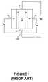
- the JFEThas two opposed gate regions 10 , a drain 11 and source 12 .
- the drain 11 and source 12are located in the n-doped region of the device and the gates 10 are p-doped.
- Two p-n junctionsare present in the device, each having an associated depletion region 13 .
- a conductive channel region 14is shown between the two depletion regions 13 associated with the p-n junctions.
- the voltage variable width of the depletion regions 13is used to control the effective cross-sectional area the of conductive channel region 14 .
- V gsvoltage between the gates 10 and source 12 will cause the conductive channel region to vary in width, thereby controlling the resistance between the drain 11 and the source 12 .
- a reverse bias(e.g., a negative V gs ), will cause the depletion regions to expand, and at a sufficiently negative value cause the conductive channel to “pinch off”, thereby turning off the device.
- the width of the depletion regions 13 and the conductive channel region 14are determined by the width of the n-doped region and the dopant levels in the n-doped and p-doped regions. If the device shown in FIG. 1 were constructed with a narrow n-doped region, such that the two depletion regions merged into a single continuous depletion region and the conductive channel region 14 had zero width, the result would be the device shown in Prior Art FIG. 2 .
- Enhancement modeor “normally off” JFETs are characterized by a channel that is sufficiently narrow such that a depletion region at zero applied voltage extends across the entire width of the channel. Application of a forward bias reduces the width of the depletion region in the channel, thereby creating a conduction path in the channel.
- P-channel enhancement mode JFETsare turned on by the application of a negative V gs
- n-channel enhancement mode JFETsare turned on by the application of a positive V gs .
- the input gate voltage of an enhancement mode JFETis limited by the forward voltage of the p-n junction.
- the enhancement mode deviceis “normally off” since the conductive channel width is zero due to the extent of the two depletion regions 13 B.
- the application of a sufficient forward bias (e.g. positive V gs ) to the device of FIG. 2will cause the depletion regions 13 B to contract, thereby opening a conductive channel.
- depletion mode and enhancement mode devices shown schematically in FIG. 1 and FIG. 2are n-channel devices, depletion mode and enhancement mode devices could be constructed with a reversed doping scheme to provide p-channel devices.
- JFETsare capable of being driven by low voltages while maintaining excellent breakdown characteristics when compared to MOSFETs. Since there is no insulator associated with gate/drain and gate/source interfaces of a JFET (only a p-n junction), forward bias results in conduction at a voltage that is very low compared to the reverse bias that the device is capable of withstanding. JFETs also have a much greater resistance to damage from electrostatic discharge (ESD) than MOSFETs.
- ESDelectrostatic discharge
- MOSFETsmetal-oxide semiconductor field effect transistors
- the vertical composition of device featurese.g., the gate and its associated p-n junctions
- the vertical composition of device featureshas remained relatively unchanged with respect to processes involving ion implantation and thermal diffusion.
- embodiments of the present inventionprovide enhanced control over the vertical characteristics of gate structures of JFETs and MESFETs.
- multiple ion implantation stepsare used to provide a dual gate structure that reduces the effective channel length, leakage current, and parasitic capacitance in JFETs and MESFETs.
- a method for fabricating a dual gate structure for JFET and MESFET devicesis disclosed. Trenches are etched in a semiconductor substrate for fabrication of a gate structure for a JFET or MESFET. A sidewall spacer may be formed on the walls of the trenches to adjust the lateral dimension for a first gate. Following the formation of the first gate, a buffer region is implanted below the first gate using a complementary dopant and a second sidewall spacer with a thickness that may be the same or greater than the thickness of the first sidewall spacer. Subsequent to the buffer implant, a second gate is implanted beneath the buffer layer using a third sidewall spacer with a greater thickness than the first sidewall spacer.
- a JFETis fabricated with two gates.
- the first gateis implanted at a first implant energy
- a second narrower gateis implanted at a higher implant energy than the first gate.
- a buffer layeris implanted between the two gates using a dopant that is complementary to the dopant used in the two gates.
- the first gateis a control gate, and the second gate may be left floating, or may be used as a second control gate.
- FIG. 1shows a general schematic for an n-channel depletion mode junction field effect transistor (JFET).
- JFETn-channel depletion mode junction field effect transistor
- FIG. 2shows a general schematic for an n-channel enhancement mode junction field effect transistor (JFET).
- JFETjunction field effect transistor
- FIG. 3Ashows a cross-sectional view of a vertical JFET substrate with trenches and sidewall spacers in accordance with an embodiment of the present claimed invention.
- FIG. 3Bshows a cross-sectional view of the substrate of FIG. 3A after the formation of a first gate region in accordance with an embodiment of the present claimed invention.
- FIG. 3Cshows a cross-sectional view of the substrate of FIG. 3B after the formation of a wide buffer layer in accordance with an embodiment of the present claimed invention.
- FIG. 3Dshows a cross-sectional view of the substrate of FIG. 3B after the formation of a narrow buffer layer in accordance with an embodiment of the present claimed invention.
- FIG. 3Eshows a cross-sectional view of the substrate of FIG. 3D after the formation of a second gate region in accordance with an embodiment of the present claimed invention.
- FIG. 3Fshows an annealed dual gate JFET structure in accordance with an embodiment of the present claimed invention.
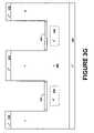
- FIG. 3Gshows an annealed dual gate MESFET structure in accordance with an embodiment of the present claimed invention.
- FIG. 4shows a process flow diagram for fabricating a dual gate structure for a FET in accordance with a method embodiment of the present claimed invention.
- FIG. 3Ashows a cross-sectional view of an n-type substrate 300 with trenches 305 and sidewall spacers 315 a on the walls of the trenches 305 .
- the sidewall spacersmay be thermally grown or deposited.
- the substrate 300comprises an n + layer 310 on the top surface to provide ohmic contact for a drain connection, and an n + layer 305 on the bottom surface to provide ohmic contact for a source connection.
- the substrate region between the two adjacent trenches 305forms the channel region for the JFET.
- siliconis used as a representative semiconductor substrate material. However, other semiconductor materials may be used (e.g., silicon carbide, gallium arsenide, or gallium nitride).
- FIG. 3Bshows a cross-sectional view of the substrate of FIG. 3A after the formation of a first gate region 320 for a JFET has been formed by low energy ion implantation of a p-type dopant (e.g., boron).
- a first gate for a MESFETmay be formed by deposition of a suitable Schottky barrier metal on the bottom of the trench 305 (see FIG. 3G ).
- the sidewall spacers 315 aserve as a mask that establishes the width of the first gate.
- FIG. 3Bshows an n-type substrate and a p-type gate implant, as is used in an n-channel device, a p-type substrate may be used to fabricate a p-channel device.
- the p-type and n-type dopantsare complementary to each other.
- FIG. 3Cshows a cross-sectional view of the substrate of FIG. 3B after the implantation of a buffer layer 325 a .
- the buffer layer 325 implantuses the same spacer 315 a that was used for the first gate formation.
- the buffer layer implanthas essentially the same width as the first gate implant (or Schottky metal).
- Buffer layer 325 auses a dopant that of the same type as the substrate 300 (e.g., phosphorus for n-type) and provides additional flexibility in tailoring the characteristics of the first gate p-n junction.
- the buffer layer 325 amay be used to effectively “trim” the first gate and thus reduce the channel length of the first gate.
- FIG. 3Dshows a cross-sectional view of the substrate 300 after the formation of a narrow buffer layer 325 b .
- the narrow buffer layeris achieved by using a relatively thick spacer 315 b.
- FIG. 3Eshows a cross-sectional view of the substrate 300 of FIG. 3D after the formation of a second p gate region 330 .
- the second gate region 330is formed by a high-energy low dose implant (e.g., boron) using a relatively thick spacer 315 b .
- the spacer used for the second gate implantis thicker than the spacer used for the formation of the first gate, and results in the second gate being narrower than the first gate.
- the second gatemay be connected as a control gate for the FET, or it may be left floating. As a floating gate, the second gate is kept narrow so that unwanted pinch off of the channel through overlapping depletion regions does not occur.
- the p-n junction associated with the second gateprovides an additional gate/drain capacitance (C gd ) that is in series with the C gd of the first gate, thus reducing the overall C gd .
- the second gatealso reduces the overall gate/drain current (I gd ).
- FIG. 3Fshows an annealed dual gate JFET structure in accordance with a first gate 320 a and a second gate 330 a .
- the dual gate structure shownis the result of three separate implants. The anneal of the implants may be done as a single step after all implants have been made, or the anneal may be done in stages interspersed with the implant steps.
- the dual gate structureis the result of a superposition of three implant steps, and provides considerable flexibility in tailoring the substrate composition in the vertical dimension to achieve particular performance characteristics for the JFET.
- FIG. 3Gshows an annealed dual gate MESFET structure having a deposited first gate 335 and an implanted second gate 330 .
- the MESFETrequires only two implants, one for the buffer layer as previously described, and one for the second gate.
- FIG. 4shows a process flow diagram 400 for fabricating a dual gate structure for a JFET or MESFET.
- trenchesare etched in the surface of a substrate.
- a sidewall spacermay be formed to establish the width of the region to be implanted for a first gate. In the absence of the sidewall spacer, the width of the implant region is essentially the width of the bottom of the trenches.
- the first gateis formed.
- the gatemay formed by depositing a metal to form a Schottky barrier on the bottom of the trench (e.g., for a MESFET), or an implant may be done to form a gate region with a p-n junction (e.g., for a JFET).
- a second sidewall spacermay be formed to establish the width of a buffer region.
- the second sidewall spacerhas a thickness that is greater than or equal to the thickness of the first sidewall spacer.
- step 425an implant is performed to form a buffer region beneath the first gate.
- the buffer regionis implanted with a dopant that is of the same type as the substrate.
- a sidewall spaceris formed for defining the width of a second gate.
- the sidewall spacer for the second gateis thicker than the sidewall spacer: used for the first gate.
- the second gate regionis implanted using a high-energy low dose implant.
- the second implantproduces a second gate that is narrower than the first gate and separated from the first gate by the buffer region.
- the implantsare annealed.
- the annealmay be done after all implants have been performed, or it may be done in stages.
- Piecewise annealingmay be used when the second gate is implanted first, followed by the buffer implant. Once annealed, the deep implant will not be subjected to knock-on damage by subsequent shallower implants.
Landscapes
- Junction Field-Effect Transistors (AREA)
Abstract
Description
Claims (14)
Priority Applications (2)
| Application Number | Priority Date | Filing Date | Title |
|---|---|---|---|
| US10/382,344US7038260B1 (en) | 2003-03-04 | 2003-03-04 | Dual gate structure for a FET and method for fabricating same |
| US10/776,487US7452763B1 (en) | 2003-03-04 | 2004-02-10 | Method for a junction field effect transistor with reduced gate capacitance |
Applications Claiming Priority (1)
| Application Number | Priority Date | Filing Date | Title |
|---|---|---|---|
| US10/382,344US7038260B1 (en) | 2003-03-04 | 2003-03-04 | Dual gate structure for a FET and method for fabricating same |
Publications (1)
| Publication Number | Publication Date |
|---|---|
| US7038260B1true US7038260B1 (en) | 2006-05-02 |
Family
ID=36216035
Family Applications (1)
| Application Number | Title | Priority Date | Filing Date |
|---|---|---|---|
| US10/382,344Expired - Fee RelatedUS7038260B1 (en) | 2003-03-04 | 2003-03-04 | Dual gate structure for a FET and method for fabricating same |
Country Status (1)
| Country | Link |
|---|---|
| US (1) | US7038260B1 (en) |
Cited By (14)
| Publication number | Priority date | Publication date | Assignee | Title |
|---|---|---|---|---|
| US20050167695A1 (en)* | 2004-02-02 | 2005-08-04 | Hamza Yilmaz | Semiconductor device containing dielectrically isolated pn junction for enhanced breakdown characteristics |
| US20080197406A1 (en)* | 2007-02-16 | 2008-08-21 | Power Integrations, Inc. | Sensing FET integrated with a high-voltage vertical transistor |
| US20080258183A1 (en)* | 2007-04-23 | 2008-10-23 | Infineon Technologies Ag | Method of manufacturing a device by locally heating one or more metallization layers and by means of selective etching |
| US20090273023A1 (en)* | 2007-02-16 | 2009-11-05 | Power Integrations, Inc. | Segmented pillar layout for a high-voltage vertical transistor |
| US20090315105A1 (en)* | 2007-02-16 | 2009-12-24 | Power Integrations, Inc. | High-voltage vertical transistor structure |
| US20120007152A1 (en)* | 2010-07-09 | 2012-01-12 | Tzu-Hsiung Chen | Low gate charging rectifier having mos structure and p-n junction, and manufacturing method of the same |
| US8410551B2 (en) | 2007-02-16 | 2013-04-02 | Power Integrations, Inc. | Checkerboarded high-voltage vertical transistor layout |
| CN103354208A (en)* | 2013-05-20 | 2013-10-16 | 泰科天润半导体科技(北京)有限公司 | Preparation method of silicon carbide grooved JFET (junction field effect transistor) |
| US20160181372A1 (en)* | 2013-07-26 | 2016-06-23 | Sumitomo Electric Industries, Ltd. | Silicon carbide semiconductor device and method for manufacturing same |
| US9543396B2 (en) | 2013-12-13 | 2017-01-10 | Power Integrations, Inc. | Vertical transistor device structure with cylindrically-shaped regions |
| US9685900B2 (en) | 2010-11-19 | 2017-06-20 | General Electric Company | Low-inductance, high-efficiency induction machine and method of making same |
| US9780716B2 (en) | 2010-11-19 | 2017-10-03 | General Electric Company | High power-density, high back emf permanent magnet machine and method of making same |
| US10325988B2 (en) | 2013-12-13 | 2019-06-18 | Power Integrations, Inc. | Vertical transistor device structure with cylindrically-shaped field plates |
| CN115360098A (en)* | 2022-10-18 | 2022-11-18 | 杭州芯迈半导体技术有限公司 | A kind of manufacturing method of trench type MOSFET |
Citations (41)
| Publication number | Priority date | Publication date | Assignee | Title |
|---|---|---|---|---|
| US3381188A (en) | 1964-08-18 | 1968-04-30 | Hughes Aircraft Co | Planar multi-channel field-effect triode |
| US4223328A (en)* | 1977-06-08 | 1980-09-16 | Hitachi, Ltd. | Field controlled thyristor with dual resistivity field layer |
| US4404575A (en) | 1979-01-22 | 1983-09-13 | Zaidan Hojin Handotai Kenkyu Shinkokai | Semiconductor device |
| US4419586A (en) | 1981-08-27 | 1983-12-06 | Motorola, Inc. | Solid-state relay and regulator |
| US4506282A (en) | 1983-01-03 | 1985-03-19 | General Electric Company | Normally-off semiconductor device with low on resistance and circuit analogue |
| US4519024A (en) | 1983-09-02 | 1985-05-21 | At&T Bell Laboratories | Two-terminal transistor rectifier circuit arrangement |
| US4523111A (en) | 1983-03-07 | 1985-06-11 | General Electric Company | Normally-off, gate-controlled electrical circuit with low on-resistance |
| US4566172A (en)* | 1984-02-24 | 1986-01-28 | Gte Laboratories Incorporated | Method of fabricating a static induction type recessed junction field effect transistor |
| US4645957A (en) | 1983-01-03 | 1987-02-24 | General Electric Company | Normally-off semiconductor device with low on resistance and circuit analogue |
| US4700461A (en) | 1986-09-29 | 1987-10-20 | Massachusetts Institute Of Technology | Process for making junction field-effect transistors |
| US4750023A (en) | 1982-05-10 | 1988-06-07 | U.S. Philips Corporation | Semiconductor devices having gate-controlled unipolar hot-carrier transistors and their manufacture |
| US4769685A (en) | 1986-10-27 | 1988-09-06 | General Motors Corporation | Recessed-gate junction-MOS field effect transistor |
| US4853561A (en) | 1987-06-10 | 1989-08-01 | Regents Of The University Of Minnesota | Family of noise-immune logic gates and memory cells |
| US5038266A (en) | 1990-01-02 | 1991-08-06 | General Electric Company | High efficiency, regulated DC supply |
| US5396085A (en) | 1993-12-28 | 1995-03-07 | North Carolina State University | Silicon carbide switching device with rectifying-gate |
| US5488236A (en)* | 1994-05-26 | 1996-01-30 | North Carolina State University | Latch-up resistant bipolar transistor with trench IGFET and buried collector |
| US5719409A (en)* | 1996-06-06 | 1998-02-17 | Cree Research, Inc. | Silicon carbide metal-insulator semiconductor field effect transistor |
| US5808328A (en)* | 1977-02-21 | 1998-09-15 | Zaidan Hojin Handotai Kenkyu Shinkokai | High-speed and high-density semiconductor memory |
| US5861643A (en)* | 1996-08-26 | 1999-01-19 | Chartered Semiconductor Manufacturing, Ltd. | Self-aligned JFET |
| US5945699A (en)* | 1997-05-13 | 1999-08-31 | Harris Corporation | Reduce width, differentially doped vertical JFET device |
| US6011703A (en) | 1997-07-30 | 2000-01-04 | Lucent Technologies Inc. | Self-synchronized gate drive for power converter employing self-driven synchronous rectifier and method of operation thereof |
| US6028778A (en) | 1997-04-04 | 2000-02-22 | Kabushiki Kaisha Tec | Power supply device with improved efficiency and reduced higher harmonics |
| US6064580A (en) | 1998-03-09 | 2000-05-16 | Shindengen Electric Manufacturing Co., Ltd. | Switching power supply |
| US6069809A (en) | 1998-05-08 | 2000-05-30 | Denso Corporation | Resonant inverter apparatus |
| US6084792A (en) | 1998-08-21 | 2000-07-04 | Vpt, Inc. | Power converter with circuits for providing gate driving |
| US6090650A (en) | 1997-09-30 | 2000-07-18 | Intel Corporation | Method to reduce timing skews in I/O circuits and clock drivers caused by fabrication process tolerances |
| US6104172A (en) | 1997-07-01 | 2000-08-15 | Power-One | Power factor corrector |
| US6180519B1 (en) | 1995-07-06 | 2001-01-30 | Mitsubishi Denki Kabushiki Kaisha | Method of forming a layered wiring structure including titanium silicide |
| US6236257B1 (en) | 1998-10-01 | 2001-05-22 | Lsi Logic Corporation | Method and apparatus for reducing using feed forward compensation |
| US6251716B1 (en) | 1999-01-06 | 2001-06-26 | Lovoltech, Inc. | JFET structure and manufacture method for low on-resistance and low voltage application |
| US6307223B1 (en) | 1998-12-11 | 2001-10-23 | Lovoltech, Inc. | Complementary junction field effect transistors |
| US6404157B1 (en) | 2000-07-27 | 2002-06-11 | John D. Simon | Circuitry using back EMF of a motor to generate a system wake up signal |
| US20020074585A1 (en)* | 1988-05-17 | 2002-06-20 | Advanced Power Technology, Inc., Delaware Corporation | Self-aligned power MOSFET with enhanced base region |
| US6439678B1 (en) | 1999-11-23 | 2002-08-27 | Hewlett-Packard Company | Method and apparatus for non-saturated switching for firing energy control in an inkjet printer |
| US6551865B2 (en)* | 2001-03-30 | 2003-04-22 | Denso Corporation | Silicon carbide semiconductor device and method of fabricating the same |
| US20030151101A1 (en)* | 1996-11-05 | 2003-08-14 | Power Integrations, Inc. | High-voltage transistor with multi-layer conduction region |
| US20030178646A1 (en)* | 2001-01-24 | 2003-09-25 | Power Integrations, Inc. | High-voltage transistor with buried conduction layer |
| US6696706B1 (en)* | 2002-10-22 | 2004-02-24 | Lovoltech, Inc. | Structure and method for a junction field effect transistor with reduced gate capacitance |
| US20040065896A1 (en)* | 2002-10-04 | 2004-04-08 | Kazuhisa Sakamoto | Junction field-effect transistor |
| US6777722B1 (en)* | 2002-07-02 | 2004-08-17 | Lovoltech, Inc. | Method and structure for double dose gate in a JFET |
| US6921932B1 (en)* | 2002-05-20 | 2005-07-26 | Lovoltech, Inc. | JFET and MESFET structures for low voltage, high current and high frequency applications |
- 2003
- 2003-03-04USUS10/382,344patent/US7038260B1/ennot_activeExpired - Fee Related
Patent Citations (43)
| Publication number | Priority date | Publication date | Assignee | Title |
|---|---|---|---|---|
| US3381188A (en) | 1964-08-18 | 1968-04-30 | Hughes Aircraft Co | Planar multi-channel field-effect triode |
| US5808328A (en)* | 1977-02-21 | 1998-09-15 | Zaidan Hojin Handotai Kenkyu Shinkokai | High-speed and high-density semiconductor memory |
| US4223328A (en)* | 1977-06-08 | 1980-09-16 | Hitachi, Ltd. | Field controlled thyristor with dual resistivity field layer |
| US4404575A (en) | 1979-01-22 | 1983-09-13 | Zaidan Hojin Handotai Kenkyu Shinkokai | Semiconductor device |
| US4419586A (en) | 1981-08-27 | 1983-12-06 | Motorola, Inc. | Solid-state relay and regulator |
| US4750023A (en) | 1982-05-10 | 1988-06-07 | U.S. Philips Corporation | Semiconductor devices having gate-controlled unipolar hot-carrier transistors and their manufacture |
| US4645957A (en) | 1983-01-03 | 1987-02-24 | General Electric Company | Normally-off semiconductor device with low on resistance and circuit analogue |
| US4506282A (en) | 1983-01-03 | 1985-03-19 | General Electric Company | Normally-off semiconductor device with low on resistance and circuit analogue |
| US4523111A (en) | 1983-03-07 | 1985-06-11 | General Electric Company | Normally-off, gate-controlled electrical circuit with low on-resistance |
| US4519024A (en) | 1983-09-02 | 1985-05-21 | At&T Bell Laboratories | Two-terminal transistor rectifier circuit arrangement |
| US4566172A (en)* | 1984-02-24 | 1986-01-28 | Gte Laboratories Incorporated | Method of fabricating a static induction type recessed junction field effect transistor |
| US4700461A (en) | 1986-09-29 | 1987-10-20 | Massachusetts Institute Of Technology | Process for making junction field-effect transistors |
| US4769685A (en) | 1986-10-27 | 1988-09-06 | General Motors Corporation | Recessed-gate junction-MOS field effect transistor |
| US4853561A (en) | 1987-06-10 | 1989-08-01 | Regents Of The University Of Minnesota | Family of noise-immune logic gates and memory cells |
| US20020074585A1 (en)* | 1988-05-17 | 2002-06-20 | Advanced Power Technology, Inc., Delaware Corporation | Self-aligned power MOSFET with enhanced base region |
| US5038266A (en) | 1990-01-02 | 1991-08-06 | General Electric Company | High efficiency, regulated DC supply |
| US5396085A (en) | 1993-12-28 | 1995-03-07 | North Carolina State University | Silicon carbide switching device with rectifying-gate |
| US5488236A (en)* | 1994-05-26 | 1996-01-30 | North Carolina State University | Latch-up resistant bipolar transistor with trench IGFET and buried collector |
| US6180519B1 (en) | 1995-07-06 | 2001-01-30 | Mitsubishi Denki Kabushiki Kaisha | Method of forming a layered wiring structure including titanium silicide |
| US5719409A (en)* | 1996-06-06 | 1998-02-17 | Cree Research, Inc. | Silicon carbide metal-insulator semiconductor field effect transistor |
| US5831288A (en)* | 1996-06-06 | 1998-11-03 | Cree Research, Inc. | Silicon carbide metal-insulator semiconductor field effect transistor |
| US5861643A (en)* | 1996-08-26 | 1999-01-19 | Chartered Semiconductor Manufacturing, Ltd. | Self-aligned JFET |
| US20030151101A1 (en)* | 1996-11-05 | 2003-08-14 | Power Integrations, Inc. | High-voltage transistor with multi-layer conduction region |
| US6028778A (en) | 1997-04-04 | 2000-02-22 | Kabushiki Kaisha Tec | Power supply device with improved efficiency and reduced higher harmonics |
| US5945699A (en)* | 1997-05-13 | 1999-08-31 | Harris Corporation | Reduce width, differentially doped vertical JFET device |
| US6104172A (en) | 1997-07-01 | 2000-08-15 | Power-One | Power factor corrector |
| US6011703A (en) | 1997-07-30 | 2000-01-04 | Lucent Technologies Inc. | Self-synchronized gate drive for power converter employing self-driven synchronous rectifier and method of operation thereof |
| US6090650A (en) | 1997-09-30 | 2000-07-18 | Intel Corporation | Method to reduce timing skews in I/O circuits and clock drivers caused by fabrication process tolerances |
| US6064580A (en) | 1998-03-09 | 2000-05-16 | Shindengen Electric Manufacturing Co., Ltd. | Switching power supply |
| US6069809A (en) | 1998-05-08 | 2000-05-30 | Denso Corporation | Resonant inverter apparatus |
| US6084792A (en) | 1998-08-21 | 2000-07-04 | Vpt, Inc. | Power converter with circuits for providing gate driving |
| US6236257B1 (en) | 1998-10-01 | 2001-05-22 | Lsi Logic Corporation | Method and apparatus for reducing using feed forward compensation |
| US6307223B1 (en) | 1998-12-11 | 2001-10-23 | Lovoltech, Inc. | Complementary junction field effect transistors |
| US6251716B1 (en) | 1999-01-06 | 2001-06-26 | Lovoltech, Inc. | JFET structure and manufacture method for low on-resistance and low voltage application |
| US6439678B1 (en) | 1999-11-23 | 2002-08-27 | Hewlett-Packard Company | Method and apparatus for non-saturated switching for firing energy control in an inkjet printer |
| US6404157B1 (en) | 2000-07-27 | 2002-06-11 | John D. Simon | Circuitry using back EMF of a motor to generate a system wake up signal |
| US20030178646A1 (en)* | 2001-01-24 | 2003-09-25 | Power Integrations, Inc. | High-voltage transistor with buried conduction layer |
| US6551865B2 (en)* | 2001-03-30 | 2003-04-22 | Denso Corporation | Silicon carbide semiconductor device and method of fabricating the same |
| US6921932B1 (en)* | 2002-05-20 | 2005-07-26 | Lovoltech, Inc. | JFET and MESFET structures for low voltage, high current and high frequency applications |
| US6777722B1 (en)* | 2002-07-02 | 2004-08-17 | Lovoltech, Inc. | Method and structure for double dose gate in a JFET |
| US20040065896A1 (en)* | 2002-10-04 | 2004-04-08 | Kazuhisa Sakamoto | Junction field-effect transistor |
| US6696706B1 (en)* | 2002-10-22 | 2004-02-24 | Lovoltech, Inc. | Structure and method for a junction field effect transistor with reduced gate capacitance |
| US6812079B1 (en)* | 2002-10-22 | 2004-11-02 | Lovoltech, Inc. | Method for a junction field effect transistor with reduced gate capacitance |
Non-Patent Citations (15)
| Title |
|---|
| "N-Channel 30V-0.034Omega-22A D2PAK STRIPFET Power MOSFET"; STB22NE03L: Preliminary Data; 6 pgs.; Nov. 2000. |
| "N-Channel Enhancement-Mode MOSFET Transistors"; 2N66601/VN88AFD; Product Summary; Siliconix; P-37655-Rev. B, Jul. 25, 1994. |
| "N-Channel Enhancement-Mode MOSFET Transistors"; 2N6660JAN/JANTX/JANTXV; Product Summary; Siliconix; P-37515-Rev. A, Jul. 4, 1994. |
| Caruso et al.; "Performance Analysis of a Bipolar Mode FET (BMFET) with Normally Off Characteristics"; IEEE Transactions on Power Electronics; vol. 3; No. 2; Apr. 1988. |
| Central Semiconductor Corp.; CMPF4391, CMPF4392 CMPF4393, N-Channel JFET; Product Summary. |
| Fairchild Semiconductor Corporation; "N-Channel/Logic Level Enhancement Mode Field Effect Transistor"; FDP6030L/FDB6030L; Apr. 1998. |
| General Semiconductor; GF2208; "N-Channel Enhancement-Mode MOSFET"; Jul. 10, 2001. |
| H. Ogiwara, M. Hayakawa, T. Nishimura and M. Nakaoka; "High-Frequency Induction Heating Inverter with Multi-Resonant Mode Using Newly Developed Normally-Off Type Static Induction Transistors"; Department of Electrical Engineering, Ashikaga Institute of Technology, Japan; Department of Electrical Engineering, Oita University, Japan; Department of Electrical Engineering, Kobe University, Japan; pp. 1017-1023. |
| International Rectifier; IRF1205; HEXFET Power MOSFET; Nov. 3, 1999. |
| J. Baliga; "Highvoltage Junction-Gate Field Effect Transistor wth Recessed Gates"; IEEE Transactions on Electron Devices; vol. ED-29; No. 10; Oct. 1982. |
| J. M. C. Stork et al.; "Small Geometry Depleted Base Bipolar Transistors (BSIT)- VLSI Devices?"; IEEE Transactions on Electron Devices; vol. ED-28; No. 11; Nov. 1981. |
| Kang et al.; "A New Type of Transistor: CBT"; IEEE Transactions on Electron Devices; vol. 40; #10; Oct. 93. |
| Nishizawa et al.; "Fieldeffect Transistor Versus Analog Transistor (Static Induction Transistor)"; IEEE Transactions on Electron Devices; vol. ED-24; No. 4; Apr. 1975. |
| Nishizawa et al.;"Analysis of Static Characteristics of a Bipolar Mode SIT (BSIT)"; IEEE Transactions on Electron Devices; vol. ED-29; No. 11; Aug. 1982. |
| Philips Semiconductors; "Powermos Transistor"; BUK463-60A/B; Product Specification; Jul. 1995. |
Cited By (31)
| Publication number | Priority date | Publication date | Assignee | Title |
|---|---|---|---|---|
| US7489011B2 (en) | 2004-02-02 | 2009-02-10 | Hamza Yilmaz | Semiconductor device containing dielectrically isolated PN junction for enhanced breakdown characteristics |
| US20050167744A1 (en)* | 2004-02-02 | 2005-08-04 | Hamza Yilmaz | Semiconductor device containing dielectrically isolated PN junction for enhanced breakdown characteristics |
| US20060065924A1 (en)* | 2004-02-02 | 2006-03-30 | Hamza Yilmaz | Semiconductor device containing dielectrically isolated PN junction for enhanced breakdown characteristics |
| US20060170036A1 (en)* | 2004-02-02 | 2006-08-03 | Hamza Yilmaz | Method of fabricating semiconductor device containing dielectrically isolated PN junction for enhanced breakdown characteristics |
| US7323386B2 (en) | 2004-02-02 | 2008-01-29 | Hamza Yilmaz | Method of fabricating semiconductor device containing dielectrically isolated PN junction for enhanced breakdown characteristics |
| US7405452B2 (en)* | 2004-02-02 | 2008-07-29 | Hamza Yilmaz | Semiconductor device containing dielectrically isolated PN junction for enhanced breakdown characteristics |
| US20050167695A1 (en)* | 2004-02-02 | 2005-08-04 | Hamza Yilmaz | Semiconductor device containing dielectrically isolated pn junction for enhanced breakdown characteristics |
| US7427800B2 (en) | 2004-02-02 | 2008-09-23 | Hamza Yilmaz | Semiconductor device containing dielectrically isolated PN junction for enhanced breakdown characteristics |
| US8410551B2 (en) | 2007-02-16 | 2013-04-02 | Power Integrations, Inc. | Checkerboarded high-voltage vertical transistor layout |
| US8552493B2 (en) | 2007-02-16 | 2013-10-08 | Power Integrations, Inc. | Segmented pillar layout for a high-voltage vertical transistor |
| US20090273023A1 (en)* | 2007-02-16 | 2009-11-05 | Power Integrations, Inc. | Segmented pillar layout for a high-voltage vertical transistor |
| US20090315105A1 (en)* | 2007-02-16 | 2009-12-24 | Power Integrations, Inc. | High-voltage vertical transistor structure |
| US8653583B2 (en) | 2007-02-16 | 2014-02-18 | Power Integrations, Inc. | Sensing FET integrated with a high-voltage transistor |
| US8222691B2 (en) | 2007-02-16 | 2012-07-17 | Power Integrations, Inc. | Gate pullback at ends of high-voltage vertical transistor structure |
| US20080197406A1 (en)* | 2007-02-16 | 2008-08-21 | Power Integrations, Inc. | Sensing FET integrated with a high-voltage vertical transistor |
| US9209281B2 (en)* | 2007-04-23 | 2015-12-08 | Infineon Technologies Ag | Method of manufacturing a device by locally heating one or more metallization layers and by means of selective etching |
| US9391154B2 (en)* | 2007-04-23 | 2016-07-12 | Infineon Technologies Ag | Method of manufacturing a device by locally heating one or more metalization layers and by means of selective etching |
| US9634108B2 (en)* | 2007-04-23 | 2017-04-25 | Infineon Technologies Ag | Method of manufacturing a device by locally heating one or more metalization layers and by means of selective etching |
| US20080258183A1 (en)* | 2007-04-23 | 2008-10-23 | Infineon Technologies Ag | Method of manufacturing a device by locally heating one or more metallization layers and by means of selective etching |
| US20120007152A1 (en)* | 2010-07-09 | 2012-01-12 | Tzu-Hsiung Chen | Low gate charging rectifier having mos structure and p-n junction, and manufacturing method of the same |
| US8415719B2 (en)* | 2010-07-09 | 2013-04-09 | Tzu-Hsiung Chen | Low gate charging rectifier having MOS structure and P-N junction, and manufacturing method of the same |
| US9685900B2 (en) | 2010-11-19 | 2017-06-20 | General Electric Company | Low-inductance, high-efficiency induction machine and method of making same |
| US9780716B2 (en) | 2010-11-19 | 2017-10-03 | General Electric Company | High power-density, high back emf permanent magnet machine and method of making same |
| US10946748B2 (en) | 2010-11-19 | 2021-03-16 | General Electric Company | High power-density, high back EMF permanent magnet machine and method of making same |
| CN103354208B (en)* | 2013-05-20 | 2016-01-06 | 泰科天润半导体科技(北京)有限公司 | The manufacture method of the groove-shaped JFET of a kind of carborundum |
| CN103354208A (en)* | 2013-05-20 | 2013-10-16 | 泰科天润半导体科技(北京)有限公司 | Preparation method of silicon carbide grooved JFET (junction field effect transistor) |
| US20160181372A1 (en)* | 2013-07-26 | 2016-06-23 | Sumitomo Electric Industries, Ltd. | Silicon carbide semiconductor device and method for manufacturing same |
| US10192960B2 (en)* | 2013-07-26 | 2019-01-29 | Sumitomo Electric Industries, Ltd. | Silicon carbide semiconductor device and method for manufacturing same |
| US9543396B2 (en) | 2013-12-13 | 2017-01-10 | Power Integrations, Inc. | Vertical transistor device structure with cylindrically-shaped regions |
| US10325988B2 (en) | 2013-12-13 | 2019-06-18 | Power Integrations, Inc. | Vertical transistor device structure with cylindrically-shaped field plates |
| CN115360098A (en)* | 2022-10-18 | 2022-11-18 | 杭州芯迈半导体技术有限公司 | A kind of manufacturing method of trench type MOSFET |
Similar Documents
| Publication | Publication Date | Title |
|---|---|---|
| US10727334B2 (en) | Lateral DMOS device with dummy gate | |
| US9947787B2 (en) | Devices and methods for a power transistor having a schottky or schottky-like contact | |
| US8207559B2 (en) | Schottky junction-field-effect-transistor (JFET) structures and methods of forming JFET structures | |
| JP5520215B2 (en) | Improved power switching transistor | |
| US6084268A (en) | Power MOSFET device having low on-resistance and method | |
| JP3666280B2 (en) | Silicon carbide vertical FET and method of manufacturing the same | |
| US20060091490A1 (en) | Self-aligned gated p-i-n diode for ultra-fast switching | |
| US7038260B1 (en) | Dual gate structure for a FET and method for fabricating same | |
| US10510869B2 (en) | Devices and methods for a power transistor having a Schottky or Schottky-like contact | |
| US20150372103A1 (en) | Split gate power semiconductor field effect transistor | |
| US6777722B1 (en) | Method and structure for double dose gate in a JFET | |
| US10262994B2 (en) | FinFET LDMOS devices with additional dynamic control | |
| JPH0371776B2 (en) | ||
| JPH0690009A (en) | Semiconductor device | |
| US7211845B1 (en) | Multiple doped channel in a multiple doped gate junction field effect transistor | |
| US5432366A (en) | P-I-N MOSFET for ULSI applications | |
| CN101689507A (en) | An extended drain transistor and a method of manufacturing the same | |
| EP3365912B1 (en) | Method of manufacturing a triple-implanted jfet | |
| US10573744B1 (en) | Self-aligned, dual-gate LDMOS transistors and associated methods | |
| JP2001060684A (en) | Semiconductor device | |
| US7452763B1 (en) | Method for a junction field effect transistor with reduced gate capacitance | |
| US7268378B1 (en) | Structure for reduced gate capacitance in a JFET | |
| US6900506B1 (en) | Method and structure for a high voltage junction field effect transistor | |
| US6344405B1 (en) | Transistors having optimized source-drain structures and methods for making the same | |
| JPS63293979A (en) | Semiconductor device |
Legal Events
| Date | Code | Title | Description |
|---|---|---|---|
| AS | Assignment | Owner name:LOVOLTECH, INC., CALIFORNIA Free format text:ASSIGNMENT OF ASSIGNORS INTEREST;ASSIGNOR:YU, HO-YUAN;REEL/FRAME:013847/0250 Effective date:20030303 | |
| AS | Assignment | Owner name:QSPEED SEMICONDUCTOR INC.,CALIFORNIA Free format text:CHANGE OF NAME;ASSIGNOR:LOVOLTECH INC.;REEL/FRAME:018597/0920 Effective date:20060410 Owner name:QSPEED SEMICONDUCTOR INC., CALIFORNIA Free format text:CHANGE OF NAME;ASSIGNOR:LOVOLTECH INC.;REEL/FRAME:018597/0920 Effective date:20060410 | |
| AS | Assignment | Owner name:QSPEED SEMICONDUCTOR INC.,CALIFORNIA Free format text:MERGER;ASSIGNOR:QSPEED SEMICONDUCTOR INC.;REEL/FRAME:018616/0298 Effective date:20060606 Owner name:QSPEED SEMICONDUCTOR INC., CALIFORNIA Free format text:MERGER;ASSIGNOR:QSPEED SEMICONDUCTOR INC.;REEL/FRAME:018616/0298 Effective date:20060606 | |
| AS | Assignment | Owner name:SILICON VALLEY BANK, CALIFORNIA Free format text:SECURITY AGREEMENT;ASSIGNOR:QSPEED SEMICONDUCTOR, INC.;REEL/FRAME:018855/0591 Effective date:20070123 | |
| AS | Assignment | Owner name:QSPEED SEMICONDUCTOR INC., CALIFORNIA Free format text:RELEASE;ASSIGNOR:SILICON VALLEY BANK;REEL/FRAME:022732/0220 Effective date:20090520 | |
| FPAY | Fee payment | Year of fee payment:4 | |
| AS | Assignment | Owner name:POWER INTEGRATIONS, INC., CALIFORNIA Free format text:ASSIGNMENT OF ASSIGNORS INTEREST;ASSIGNOR:QSPEED SEMICONDUCTOR, INC;REEL/FRAME:025949/0001 Effective date:20101231 | |
| FPAY | Fee payment | Year of fee payment:8 | |
| FEPP | Fee payment procedure | Free format text:MAINTENANCE FEE REMINDER MAILED (ORIGINAL EVENT CODE: REM.) | |
| LAPS | Lapse for failure to pay maintenance fees | Free format text:PATENT EXPIRED FOR FAILURE TO PAY MAINTENANCE FEES (ORIGINAL EVENT CODE: EXP.) | |
| STCH | Information on status: patent discontinuation | Free format text:PATENT EXPIRED DUE TO NONPAYMENT OF MAINTENANCE FEES UNDER 37 CFR 1.362 | |
| FP | Lapsed due to failure to pay maintenance fee | Effective date:20180502 |