US7037846B2 - Method and apparatus for micro-jet enabled, low energy ion generation and transport in plasma processing - Google Patents
Method and apparatus for micro-jet enabled, low energy ion generation and transport in plasma processingDownload PDFInfo
- Publication number
- US7037846B2 US7037846B2US10/752,906US75290604AUS7037846B2US 7037846 B2US7037846 B2US 7037846B2US 75290604 AUS75290604 AUS 75290604AUS 7037846 B2US7037846 B2US 7037846B2
- Authority
- US
- United States
- Prior art keywords
- plasma
- wafer
- baffle plate
- ions
- plasma discharge
- Prior art date
- Legal status (The legal status is an assumption and is not a legal conclusion. Google has not performed a legal analysis and makes no representation as to the accuracy of the status listed.)
- Expired - Lifetime, expires
Links
- 238000000034methodMethods0.000titleclaimsabstractdescription45
- 150000002500ionsChemical class0.000claimsabstractdescription59
- 230000000153supplemental effectEffects0.000claimsabstractdescription19
- 239000004065semiconductorSubstances0.000claimsabstractdescription14
- 230000005684electric fieldEffects0.000claimsabstractdescription8
- 230000003213activating effectEffects0.000claimsabstractdescription3
- 229910052594sapphireInorganic materials0.000claimsdescription12
- 239000010980sapphireSubstances0.000claimsdescription12
- 239000010453quartzSubstances0.000claimsdescription11
- VYPSYNLAJGMNEJ-UHFFFAOYSA-Nsilicon dioxideInorganic materialsO=[Si]=OVYPSYNLAJGMNEJ-UHFFFAOYSA-N0.000claimsdescription11
- 229910052782aluminiumInorganic materials0.000claimsdescription3
- XAGFODPZIPBFFR-UHFFFAOYSA-NaluminiumChemical compound[Al]XAGFODPZIPBFFR-UHFFFAOYSA-N0.000claimsdescription3
- 239000000919ceramicSubstances0.000claimsdescription3
- 230000002708enhancing effectEffects0.000claimsdescription2
- 239000004020conductorSubstances0.000claims3
- 235000012431wafersNutrition0.000description68
- 208000028659dischargeDiseases0.000description26
- 230000008569processEffects0.000description25
- 239000007789gasSubstances0.000description20
- 229920002120photoresistant polymerPolymers0.000description17
- 238000010849ion bombardmentMethods0.000description12
- 239000000758substrateSubstances0.000description12
- 239000000203mixtureSubstances0.000description10
- 239000000463materialSubstances0.000description8
- 230000015572biosynthetic processEffects0.000description7
- 230000001965increasing effectEffects0.000description6
- YCKRFDGAMUMZLT-UHFFFAOYSA-NFluorine atomChemical compound[F]YCKRFDGAMUMZLT-UHFFFAOYSA-N0.000description4
- PNEYBMLMFCGWSK-UHFFFAOYSA-Naluminium oxideInorganic materials[O-2].[O-2].[O-2].[Al+3].[Al+3]PNEYBMLMFCGWSK-UHFFFAOYSA-N0.000description4
- 238000001816coolingMethods0.000description4
- 229910052731fluorineInorganic materials0.000description4
- 239000011737fluorineSubstances0.000description4
- 230000007246mechanismEffects0.000description4
- 238000004380ashingMethods0.000description3
- 230000000694effectsEffects0.000description3
- 238000005530etchingMethods0.000description3
- 230000007935neutral effectEffects0.000description3
- IJGRMHOSHXDMSA-UHFFFAOYSA-NnitrogenSubstancesN#NIJGRMHOSHXDMSA-UHFFFAOYSA-N0.000description3
- 238000011144upstream manufacturingMethods0.000description3
- RYGMFSIKBFXOCR-UHFFFAOYSA-NCopperChemical compound[Cu]RYGMFSIKBFXOCR-UHFFFAOYSA-N0.000description2
- 229920006362Teflon®Polymers0.000description2
- 230000001133accelerationEffects0.000description2
- QVGXLLKOCUKJST-UHFFFAOYSA-Natomic oxygenChemical compound[O]QVGXLLKOCUKJST-UHFFFAOYSA-N0.000description2
- 238000006243chemical reactionMethods0.000description2
- 238000011109contaminationMethods0.000description2
- 229910052802copperInorganic materials0.000description2
- 239000010949copperSubstances0.000description2
- 229910052593corundumInorganic materials0.000description2
- 230000007423decreaseEffects0.000description2
- 239000003989dielectric materialSubstances0.000description2
- 238000010438heat treatmentMethods0.000description2
- 230000001939inductive effectEffects0.000description2
- 229910052757nitrogenInorganic materials0.000description2
- -1polytetrafluoroethylenePolymers0.000description2
- 229920001343polytetrafluoroethylenePolymers0.000description2
- 239000004810polytetrafluoroethyleneSubstances0.000description2
- 230000005855radiationEffects0.000description2
- 239000002904solventSubstances0.000description2
- 238000004544sputter depositionMethods0.000description2
- 239000000126substanceSubstances0.000description2
- 238000006557surface reactionMethods0.000description2
- 230000007723transport mechanismEffects0.000description2
- XLYOFNOQVPJJNP-UHFFFAOYSA-NwaterSubstancesOXLYOFNOQVPJJNP-UHFFFAOYSA-N0.000description2
- 229910001845yogo sapphireInorganic materials0.000description2
- 206010013496Disturbance in attentionDiseases0.000description1
- UFHFLCQGNIYNRP-UHFFFAOYSA-NHydrogenChemical compound[H][H]UFHFLCQGNIYNRP-UHFFFAOYSA-N0.000description1
- 230000004913activationEffects0.000description1
- 230000004323axial lengthEffects0.000description1
- 230000008901benefitEffects0.000description1
- 230000008859changeEffects0.000description1
- 238000002144chemical decomposition reactionMethods0.000description1
- 238000001311chemical methods and processMethods0.000description1
- 239000002826coolantSubstances0.000description1
- 239000013078crystalSubstances0.000description1
- 230000007812deficiencyEffects0.000description1
- 238000009792diffusion processMethods0.000description1
- 230000003292diminished effectEffects0.000description1
- 238000009826distributionMethods0.000description1
- 125000001153fluoro groupChemical groupF*0.000description1
- 229920002313fluoropolymerPolymers0.000description1
- 239000004811fluoropolymerSubstances0.000description1
- 230000004907fluxEffects0.000description1
- 229910052736halogenInorganic materials0.000description1
- 230000009931harmful effectEffects0.000description1
- 239000001257hydrogenSubstances0.000description1
- 229910052739hydrogenInorganic materials0.000description1
- 238000005468ion implantationMethods0.000description1
- 238000002955isolationMethods0.000description1
- 238000004519manufacturing processMethods0.000description1
- 229910052751metalInorganic materials0.000description1
- 239000002184metalSubstances0.000description1
- 238000012986modificationMethods0.000description1
- 230000004048modificationEffects0.000description1
- QJGQUHMNIGDVPM-UHFFFAOYSA-Nnitrogen groupChemical group[N]QJGQUHMNIGDVPM-UHFFFAOYSA-N0.000description1
- 230000003287optical effectEffects0.000description1
- 238000013021overheatingMethods0.000description1
- 239000001301oxygenSubstances0.000description1
- 229910052760oxygenInorganic materials0.000description1
- 239000002245particleSubstances0.000description1
- 238000000206photolithographyMethods0.000description1
- 230000000176photostabilizationEffects0.000description1
- 239000000376reactantSubstances0.000description1
- 230000009467reductionEffects0.000description1
- 239000011347resinSubstances0.000description1
- 229920005989resinPolymers0.000description1
- 239000000523sampleSubstances0.000description1
- 230000011218segmentationEffects0.000description1
- 238000004513sizingMethods0.000description1
- TXEYQDLBPFQVAA-UHFFFAOYSA-NtetrafluoromethaneChemical compoundFC(F)(F)FTXEYQDLBPFQVAA-UHFFFAOYSA-N0.000description1
- 229910052721tungstenInorganic materials0.000description1
- 239000010937tungstenSubstances0.000description1
Images


Classifications
- H—ELECTRICITY
- H01—ELECTRIC ELEMENTS
- H01L—SEMICONDUCTOR DEVICES NOT COVERED BY CLASS H10
- H01L21/00—Processes or apparatus adapted for the manufacture or treatment of semiconductor or solid state devices or of parts thereof
- H01L21/02—Manufacture or treatment of semiconductor devices or of parts thereof
- H01L21/04—Manufacture or treatment of semiconductor devices or of parts thereof the devices having potential barriers, e.g. a PN junction, depletion layer or carrier concentration layer
- H01L21/18—Manufacture or treatment of semiconductor devices or of parts thereof the devices having potential barriers, e.g. a PN junction, depletion layer or carrier concentration layer the devices having semiconductor bodies comprising elements of Group IV of the Periodic Table or AIIIBV compounds with or without impurities, e.g. doping materials
- H01L21/30—Treatment of semiconductor bodies using processes or apparatus not provided for in groups H01L21/20 - H01L21/26
- H01L21/302—Treatment of semiconductor bodies using processes or apparatus not provided for in groups H01L21/20 - H01L21/26 to change their surface-physical characteristics or shape, e.g. etching, polishing, cutting
- H01L21/306—Chemical or electrical treatment, e.g. electrolytic etching
- H01L21/3065—Plasma etching; Reactive-ion etching
- H—ELECTRICITY
- H01—ELECTRIC ELEMENTS
- H01J—ELECTRIC DISCHARGE TUBES OR DISCHARGE LAMPS
- H01J37/00—Discharge tubes with provision for introducing objects or material to be exposed to the discharge, e.g. for the purpose of examination or processing thereof
- H01J37/32—Gas-filled discharge tubes
- H01J37/32009—Arrangements for generation of plasma specially adapted for examination or treatment of objects, e.g. plasma sources
- H01J37/32192—Microwave generated discharge
- H—ELECTRICITY
- H01—ELECTRIC ELEMENTS
- H01J—ELECTRIC DISCHARGE TUBES OR DISCHARGE LAMPS
- H01J37/00—Discharge tubes with provision for introducing objects or material to be exposed to the discharge, e.g. for the purpose of examination or processing thereof
- H01J37/32—Gas-filled discharge tubes
- H01J37/32009—Arrangements for generation of plasma specially adapted for examination or treatment of objects, e.g. plasma sources
- H01J37/32082—Radio frequency generated discharge
- H01J37/321—Radio frequency generated discharge the radio frequency energy being inductively coupled to the plasma
Definitions
- the present inventionrelates generally to the plasma processing of semiconductor wafers and, more specifically, to a low-energy ion generation and transport mechanism for use in plasma ashing systems.
- photolithography techniquesare used to form integrated circuit patterns on a substrate.
- a semiconductor substrateis coated with a photoresist material, portions of which are exposed to ultraviolet (UV) radiation through a mask to image a desired circuit pattern on the photoresist.
- UV radiationultraviolet
- the portions of the photoresist left unexposed to the UV radiationare removed by a processing solution, leaving only the exposed portions on the substrate. In certain instances, these remaining exposed portions are baked using UV light during a photostabilization process to enable the photoresist to withstand subsequent processing.
- the photoresistis “ashed” or “burned” in the presence of atomic oxygen and other gases, and the ashed or burned photoresist, along with the residue, is “stripped” or “cleaned” from the surface of the substrate.
- One manner of removing photoresist and residuesis by directing a radio frequency (RF) energized or microwave-energized plasma at the substrate surface.
- RFradio frequency
- the plasmais formed by a gas mixture that is transported through a plasma tube that passes through a resonant microwave cavity. Microwave energy within the cavity is introduced into the plasma tube to excite the gas mixture therein and form a plasma.
- the exited plasma exhaust containing reactive speciespasses from the tube into a process chamber, in which resides a photoresist-coated semiconductor substrate to be ashed.
- This type of asheris known as a “downstream asher”, where the resist coated substrate is physically removed from the plasma generator, which is known as an “upstream” plasma source.
- a known method for enhancing the ash rate of the carbonized crust at low temperaturesemploys the use of ion bombardment.
- a conventional ion source in an asheruses a platen (or electrostatic chuck), which is typically biased at radio frequency (RF) by an RF source. Once activated, the RF source creates a capacitive discharge above the wafer. This secondary discharge then creates ion-electron pairs immediately above the wafer, from which ions are then accelerated by a capacitive “sheath” created above the wafer surface. Because the capacitive sheath may have an electric field potential as high as 40–50 eV or higher, the ions may strike the wafer at these high energies. However, such high-energy ion bombardment can cause extensive damage to the devices formed on the wafers. Also, the extensive heating of the wafer due to the heavy ion bombardment may lead to inconsistent wafer temperatures between wafer to wafer operations.
- the methodincludes generating plasma from a gas species to produce a plasma exhaust.
- the plasma exhaustis then introduced into a processing chamber containing the wafer.
- the ion content of the plasma exhaustis enhanced by activating a supplemental ion source as the plasma is introduced into the processing chamber, thereby creating a primary plasma discharge therein.
- the primary plasma dischargeis directed into a baffle plate assembly, where a secondary plasma discharge is created as the plasma exits the baffle plate assembly.
- the strength of the sheath potential exerted on ions contained in the secondary plasma dischargeis reduced, the sheath potential resulting from the primary plasma discharge.
- the resulting reduced strength of the electric fieldaccelerates the ions through a lower potential, thereby causing ion bombardment on the wafer at an energy insufficient to cause damage to semiconductor devices formed on the wafer.
- the reduction of acceleration of ions through the sheath potential in the secondary plasma dischargeis achieved by locating the supplemental ion source so as to have the baffle plate assembly disposed between the primary plasma discharge and the wafer.
- the baffle plate assemblyis configured so as to cause the secondary plasma discharge to be shaped in substantially a micro-jet formation.
- the baffle plate assemblyincludes an upper baffle plate and a lower baffle plate, with said lower baffle plate further having a plurality of chamfered holes located therethrough, to provide uniform ion impingement on the surface of the wafer, thereby preventing charging effects from damaging the wafer.
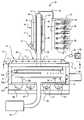
- FIG. 1is a schematical cross-sectional view of a plasma source and supplemental ion energizer which may be used with a process chamber of a photoresist asher;
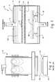
- FIG. 2is a cross-sectional view of the supplemental ion energizer of shown in FIG. 1 , taken along the line 2 — 2 ;
- FIG. 3is a cross-sectional view of an alternative embodiment of the supplemental ion energizer in FIG. 2 ;
- FIG. 4illustrates a conventional plasma ashing system having a supplemental ion source, and a high-energy capacitive sheath created directly above a semiconductor wafer when an RF biased electrostatic chuck is activated to generate the ions;
- FIG. 5is a cross-sectional schematic of the process chamber of FIG. 1 , illustrating the isolation of the high-energy capacitive sheath from the semiconductor wafer, in accordance with an embodiment of the invention
- FIG. 6is a top view of a baffle plate assembly in accordance with an embodiment of the invention.
- FIG. 7is a side cross-sectional view of the baffle plate assembly shown in FIG. 6 , taken along the line 7 — 7 ;
- FIG. 8is a top cross-sectional view of the lower baffle plate of the baffle plate assembly, taken along the line 8 — 8 ;
- FIG. 9is a cross-sectional, detailed view of the chamfered holes of the lower baffle plate.
- FIG. 10is a schematic illustrating the micro-jet, low-energy ion formation through the chamfered holes of the lower baffle plate.
- a novel low-energy ion generation and transport mechanismis disclosed herein; this mechanism enhances the chemical decomposition and subsequent volatilization of a carbonized top layer of an ion-implanted photoresist in a uniform manner, without also exposing the wafer to the potentially harmful effects of high-energy ion bombardment due to high sheath voltages.
- Such a “soft” ion assisted techniquetakes advantage of the synergy between the ions generated by a supplemental ion source in the ash tool and the chemical reactants already present, thereby producing a faster reaction than can be achieved by either, or the simple sum of these components.
- the ionscontribute both “physical” kinetic energy, as well as “chemical” internal energy released upon reaction, thereby effectively lowering the activation energy for surface reactions.
- the ionsBy shielding the wafer from the high sheath potentials characteristic of a conventional capacitive discharge, the ions are subjected to a substantially weaker electric field when passing through the sheath potential formed at the wafer.
- the ionsstrike the wafer at energies that are insufficient to do significant damage to the wafer devices, but still enable the ion-assisted chemical process of removing a carbonized crust formed on implanted photoresist.
- This schemeis also particularly suited for systems that do not need a wafer chuck for operation.
- ion implanted resistis mentioned here as an example of an application for soft ion bombardment, many other applications of such ion bombardment may be foreseen. This includes, but is not limited to removal of post etch residue, anisotropic resist removal, selective removal of photoresist in the presence of low-k material, anisotropic etch, etc.
- FIG. 1there is shown schematic of a photoresist asher 10 , in accordance with an embodiment of the invention.
- Asher 10includes a gas box 12 , a microwave power generator assembly 14 , a process chamber 16 in which is heated a semiconductor substrate or workpiece such as a wafer 18 , and a radiant heater assembly 20 (for heating the wafer 18 ) situated at the bottom of the process chamber 16 .
- a temperature probe 24such as a thermocouple, is used to monitor the temperature of the wafer 18 .
- a vacuum pump 26is used to evacuate the process chamber 16 for processes requiring vacuum conditions.
- a monochromator 28is used to monitor the optical emission characteristics of gases within the chamber to aid in process endpoint determination.
- a desired mixture of gasesis introduced into a plasma tube 32 from gas box 12 through an inlet conduit 34 .
- the plasma tube 32is made of a material such as quartz or sapphire.
- the gases forming the desired mixtureare stored in separate supplies (not shown) and mixed in the gas box 12 by means of valves 36 and piping 38 .
- a desired gas mixtureis nitrogen-based forming gas (primarily nitrogen with a small percentage of hydrogen) with or without oxygen.
- a fluorine containing gassuch as carbon tetrafluoride may be added to the gas mixture to improve ashing rates for certain processes.
- sapphireis a preferred material for plasma tube 32 .
- Sapphireresists the etching of the inner surface of plasma tube 32 , caused by the presence of reactive fluorine atoms and ions in the plasma. Additional details regarding the use of sapphire in fluorine assisted stripping may be found in U.S. Pat. No. 6,082,374 to Huffman, et al., the contents of which are incorporated herein by reference.
- the desired gas mixtureis energized by the microwave power generator assembly 14 to form a reactive plasma that will ash photoresist on the wafer 18 in the process chamber 16 when heated by the radiant heater assembly 20 .
- a magnetron 40generates microwave energy (at about 2.45 GHz) which is coupled to a waveguide 42 .
- the microwave energyis then fed from the waveguide through apertures (not shown) in a microwave enclosure 44 , which surrounds the plasma tube 32 .
- the desired gas mixturemay be energized by a radio frequency (RF) power source (not shown) in place of magnetron 40 , as is known in the art.
- RFradio frequency
- the plasma tube 32is made of alumina (Al2O3) or single crystal sapphire to accommodate fluorine plasma chemistries.
- An outer quartz cooling tube 46surrounds the sapphire plasma tube 32 , and is slightly separated therefrom. Pressurized air is fed into the gap between the tubes 32 and 46 to effectively cool the plasma tube 32 during operation.
- the microwave enclosure 44is segmented into sections shown by phantom lines 45 . Segmentation of the enclosure 44 allows uniform microwave power distribution across the length of the tube 32 , and protects it from overheating by preventing an unacceptably large thermal gradient from developing along its axial length when suitable input power is provided. Unlike quartz, sapphire is inclined to crack when heated unevenly.
- each segment of the enclosure 44is separately fed with microwave energy that passes through the quartz tube 46 and the sapphire plasma tube 32 passing therethrough. Additional details regarding this enclosure maybe found in U.S. Pat. No. 5,961,851 to Kamarehi, et al., the contents of which are incorporated herein by reference. Alternatively, a microwave applicator with a single resonant cavity specially designed to resonate in the TM012 mode may be used. Additional details regarding such an applicator may be found in U.S. Pat. No. 6,057,645 to Srivastava, et al., the contents of which are incorporated herein by reference.
- Microwave traps 48 and 50are provided at the ends of the microwave enclosure 44 to prevent microwave leakage.
- a conventional downstream asherdeliberately generates a plasma upstream from the substrate, such that the “afterglow” plasma impinging on the substrate is rich in reactive atomic species but has a poor concentration of ions.
- a supplemental ion source 74therefore, generates another plasma closer to the substrate having a substantial ionized content impinging on the surface of the wafer.
- the supplemental ion source 74may be independently operable from the plasma generated by microwave power generator assembly 14 to accommodate different plasma characteristic requirements (e.g., low ion content or high ion content) within separate steps of a single process. It will be further appreciated that the supplemental ion source 74 may be incorporated into any type of upstream plasma based asher.
- the supplemental ion source 74is provided in the form of a coil antenna assembly 76 located between a dielectric window 52 and the plasma tube 32 .
- a planar antennacan be used.
- the dielectric window 52 in asher 10is made of quartz or a similar dielectric material (like the ceramic alumina Al2O3) so that the signal emitted by coil antenna assembly 76 may pass therethrough and into the process chamber 16 .
- the coil antenna assembly 76has a metallic (e.g., copper) coil antenna 78 embedded within a base 80 .
- the base 80is preferably made of a fluoropolymer resin such as polytetrafluoroethylene (PFTE), more commonly referred to as Teflon®.
- PFTEpolytetrafluoroethylene
- Teflon®is a registered trademark of E.I. du Pont de Nemours and Company.
- the coil antenna 78should preferably reside outside of the process chamber 16 so that there is no contact with the energetic plasma, and no resulting particulate or sputtered metal contamination problem.
- the coil antenna 78which is generally planar in shape, is also sufficiently large so as to cover the entirety (or substantially the entirety) of wafer 18 .
- the antenna 78is energized by an RF signal output from RF signal generator 82 .
- the RF signaloperates at 13.56 megahertz (MHz).
- the operating frequencymay be any radio frequency that is permitted within the ISM bands.
- Disposed between the RF signal generator 87 and the antenna 78is a matching network 84 that minimizes reflected power from the antenna 78 back into the RF generator 82 .
- the connections between the RF generator 82 and the matching network 84 , as well as between the matching network 84 and antenna 78may be made with coaxial cables or waveguides. Alternatively, other mechanisms of energizing the coil may be used, such as a self-contained, frequency-tuned RF generator and amplifier.
- FIG. 3illustrates an alternative embodiment of the supplemental ion source 74 , which is provided in the form of a plate antenna assembly 90 .
- the plate antenna assembly 90has a metallic (e.g., copper or aluminum) plate antenna 92 that is generally circular in shape, and is provided with a central aperture 93 for alignment with plasma tube 32 .
- the plate antenna 92which is also generally planar in shape, is again sufficiently large to cover the entirety (or substantially the entirety) of wafer 18 .
- the resulting plasma discharge supplemented by antenna assembly 90is primarily capacitive in nature, whereas the plasma discharge supplemented by antenna assembly 76 is partially inductive.
- FIG. 1shows the use of an RF source for the supplemental energizer
- the use of other energizing (e.g., microwave) sourcesis contemplated for the supplemental ion energizer 74 .
- the energized plasmaenters the process chamber 16 through an opening 51 in the dielectric window 52 .
- An apertured, dual-layered baffle plate assembly 54comprised of upper baffle plate 54 a and lower baffle plate 54 b , evenly distributes the reactive plasma across the surface of the wafer 18 being processed.
- the radiant heater assembly 20comprises a plurality of tungsten halogen lamps 58 residing in a reflector 64 that reflects and redirects the heat generated by the lamps toward the backside of the wafer 18 positioned within the process chamber 16 on quartz pins 68 .
- thermocouple 24being in close contact with the wafer 18 , provides a feedback loop to lamps 58 , such that active temperature control of the wafer 18 may be maintained.
- One or more temperature sensors 72are mounted on the exterior of dielectric window 52 to provide an indication of chamber temperature.
- the semiconductor wafer 102is typically secured upon a chuck 104 , as shown in FIG. 4 .
- the chuck 104is typically biased at a certain RF potential (in order to provide supplemental ion generation), and a capacitive plasma is created directly above the wafer 102 .
- the wafer 102 and chuck 104are then enveloped in an energetic capacitive sheath 106 .
- This energetic sheath 106elevates the plasma to a positive potential relative to the wafer, and hence the ions (that are mostly positively charged having lost one or more electrons) are then attracted to the surface of wafer 102 .
- the potential of the sheath 106is the mechanism by which the ions are accelerated at high energy and thus bombard the wafer 102 .
- the present invention embodimentsallow the wafer to be protected from the formation of a high-energy sheath.
- a dense plasmais formed near the wafer.
- FIG. 5there is shown a cross-sectional schematic of the process chamber 16 , illustrating the capacitive sheath created during the plasma process.
- the wafer 18being mounted on quartz pins 68 (and thermocouple 24 ), is not biased at RF potentials.
- the RF antenna 74ignites an energetic capacitive (or a combination of inductive and capacitive) discharge with its associated energetic sheath 106 .
- the sheath 106(created due to the primary RF discharge) is located on the opposite side of baffle plate assembly 54 as the wafer 18 .
- wafer 18is not subjected to high-energy ions accelerated by energetic sheath 106 . Instead, the ions diffuse to the wafer 18 and impact the wafer 18 with a maximum energy associated with a “floating potential” sheath 108 surrounding wafer 18 .
- the sheaths formed between the baffle plates in baffle plate assembly 54 (and the holes therein), nor the plasmaare shown in FIG. 5 .
- baffle plate assembly 54includes the upper baffle plate 54 a , made from a dielectric material such as quartz or ceramic.
- the upper baffle plate 54 amay also be coated with sapphire so as to make it resistive to fluorine related etching.
- upper baffle plate 54 ahas an impingement disk 110 disposed at the center thereof. The impingement disk 110 causes the primary plasma discharge to impinge thereupon and stream through openings 112 in the upper baffle plate 54 a and into an interior plenum 113 in a uniform manner, as seen in FIG. 7 .
- Baffle plate assembly 54further includes a lower baffle plate 54 b , preferably made from a material such as anodized aluminum, and is grounded to act as the opposing capacitive electrode to antenna 78 or 92 .
- Lower baffle plate 54 balso has a plurality of holes 114 therein, through which a secondary plasma discharge exits.
- the holes 114 in lower baffle plate 54 bare preferably equivalent in number with the openings 112 in upper baffle plate 54 a , and are spatially aligned with respect to one another.
- a series of channels or grooves 116run in a generally V-shaped configuration through the lower baffle plate 54 b and in between the holes 114 .
- the channels 116provide a cooling mechanism for baffle plate assembly 54 by the circulation of water or other coolant material therethrough. It will be noted that the channels 116 and holes 114 are configured so as to prevent any channel 116 from being punctured and causing leaks.
- Each hole 114has a first diameter d 1 on an inner surface 118 (or plenum side) of lower baffle plate 54 b and a second diameter d 2 on an outer surface 120 (or wafer side) of lower baffle plate 54 b .
- the first diameter d 1is larger than the second diameter d 2 .
- the plenum side of the holes 114are generally frustoconical in shape, being tapered inward by a 90 degree chamfer until the interior diameter thereof is equal to d 2 .
- holes 114may be characterized as having both a frustoconical section 117 and a cylindrical section 119 .
- the cylindrical section 119 of hole 114has a height represented by d 3 in FIG. 9 .
- FIG. 10illustrates the micro-jet, low-energy ion generation region through the chamfered holes 114 of the lower baffle plate 54 b .
- a local sheath 122is created in the holes 114 , thereby resulting in an electric field.
- Electrons and ions from the primary dischargeenter the holes 114 and create a current path (indicated by dashed arrows 123 ) through each hole and to the outer surface 120 of the lower baffle plate 54 b .
- the current densityincreases causing the formation of a denser plasma in the hole, thereby forming the plasma jet which has a narrow plasma sheath.
- the increased plasma density of the microjetmay also increase the neutral temperature which reduces the density of neutrals in the holes. The combination of these effects may increase the electron temperature and change the chemistry of the discharge in the micro-jet.
- the ionsare also accelerated by the sheath and strike the inner surface 124 of the holes 114 , thereby ejecting secondary electrons.
- the narrower sheaths associated with high plasma densitypermit the acceleration of the electrons across the sheath 122 with few collisions resulting in the creation of very energetic electrons in the micro-jet.
- the secondary electronsgain enough energy so as to collide with neutral gas molecules, thereby ionizing them and creating a micro-jet shaped discharge 126 through the holes.
- the formation of micro-jets in the grounded baffle plate 54 bhas the unique property of increasing the plasma density near the larger area electrode.
- the plasma densityis highest at the smaller electrodes because of the higher electric fields and greater RF current density at the smaller electrode, this smaller electrode being where the wafer resides.
- the use of the perforated lower baffle plate 54 b as an electrode with holes therein that facilitate micro-jet formationincreases the plasma density and power dissipation at the larger area electrode. The greater density decreases the plasma sheath thickness, thereby increasing the capacitance across the sheath and increasing the effective area ratio between the lower baffle plate 54 b and the antenna 78 or 92 .
- the increased area ratiodecreases the ion bombardment energy of the baffle plate which minimizes the sputtering of the baffle plate and corresponding contamination of the wafer with sputtering products.
- the increased plasma density in the region of the lower baffle plate 54 b near the wafer and greater electron temperatureincreases both the ion bombardment flux of the wafer and can induce unique plasma chemistries. Thereby, surface reactions are possible on the wafer that could not have otherwise occurred without the micro-jets. This ion bombardment occurs in a uniform manner such that charging effects on the wafer are mitigated.
- the micro-jet discharge 126is the primary source of ions that ultimately impinge on the wafer. Because the wafer is biased at its floating potential (and not that of the RF capacitive-electrode sheath potential of the secondary discharge as in conventional ashers), the ions strike the wafer at energies insufficient to cause damage. In addition, it has also been empirically determined that a low aspect ratio (diameter d 2 divided by height d 3 ) of the holes 114 enhances the micro-jet discharge. However, if the height of the holes 114 (i.e., thickness of the lower baffle plate 54 b ) is made too small, the capacity for water cooling of the lower baffle plate is eliminated.
- the holes 114 of the present invention embodiment(s)are configured so as to provide a lower aspect ratio for effective generation and transport of an ion rich plasma, through the holes to the wafer, while still allowing effective baffle plate cooling.
- the sizing and aspect ratio of the holes 114 needed to generate reliable micro-jets thereinis a function of the process conditions, including parameters such as plasma power, pressure, gas composition, etc.
- the “lighting” of micro-jets in the holes 114is required to achieve uniform processing.
- the process describedachieves the uniform and reliable lighting of the micro-jets to produce such uniform processing.
- Thisdiffers from other applications, such as etch tunnels, in which a perforated plate with smaller holes that do not reliably form micro-jets is used to create a “field-free region” within the tunnel where wafers can be processed with minimal ion bombardment.
- the present invention embodimentsdiffer from other prior art wherein a perforated plate with larger holes is used to make a simple capacitive electrode in which the plasma passes through the holes in the plate without the formation of micro-jets.
Landscapes
- Engineering & Computer Science (AREA)
- Physics & Mathematics (AREA)
- Plasma & Fusion (AREA)
- Chemical & Material Sciences (AREA)
- Analytical Chemistry (AREA)
- Condensed Matter Physics & Semiconductors (AREA)
- Computer Hardware Design (AREA)
- Microelectronics & Electronic Packaging (AREA)
- Power Engineering (AREA)
- Manufacturing & Machinery (AREA)
- General Physics & Mathematics (AREA)
- Drying Of Semiconductors (AREA)
- Plasma Technology (AREA)
Abstract
Description
Claims (11)
Priority Applications (1)
| Application Number | Priority Date | Filing Date | Title |
|---|---|---|---|
| US10/752,906US7037846B2 (en) | 2001-04-06 | 2004-01-06 | Method and apparatus for micro-jet enabled, low energy ion generation and transport in plasma processing |
Applications Claiming Priority (3)
| Application Number | Priority Date | Filing Date | Title |
|---|---|---|---|
| US82805501A | 2001-04-06 | 2001-04-06 | |
| US09/905,043US6761796B2 (en) | 2001-04-06 | 2001-07-13 | Method and apparatus for micro-jet enabled, low-energy ion generation transport in plasma processing |
| US10/752,906US7037846B2 (en) | 2001-04-06 | 2004-01-06 | Method and apparatus for micro-jet enabled, low energy ion generation and transport in plasma processing |
Related Parent Applications (1)
| Application Number | Title | Priority Date | Filing Date |
|---|---|---|---|
| US09/905,043DivisionUS6761796B2 (en) | 2001-04-06 | 2001-07-13 | Method and apparatus for micro-jet enabled, low-energy ion generation transport in plasma processing |
Publications (2)
| Publication Number | Publication Date |
|---|---|
| US20040140053A1 US20040140053A1 (en) | 2004-07-22 |
| US7037846B2true US7037846B2 (en) | 2006-05-02 |
Family
ID=25420214
Family Applications (2)
| Application Number | Title | Priority Date | Filing Date |
|---|---|---|---|
| US09/905,043Expired - LifetimeUS6761796B2 (en) | 2001-04-06 | 2001-07-13 | Method and apparatus for micro-jet enabled, low-energy ion generation transport in plasma processing |
| US10/752,906Expired - LifetimeUS7037846B2 (en) | 2001-04-06 | 2004-01-06 | Method and apparatus for micro-jet enabled, low energy ion generation and transport in plasma processing |
Family Applications Before (1)
| Application Number | Title | Priority Date | Filing Date |
|---|---|---|---|
| US09/905,043Expired - LifetimeUS6761796B2 (en) | 2001-04-06 | 2001-07-13 | Method and apparatus for micro-jet enabled, low-energy ion generation transport in plasma processing |
Country Status (9)
| Country | Link |
|---|---|
| US (2) | US6761796B2 (en) |
| EP (1) | EP1410418B1 (en) |
| JP (1) | JP5041114B2 (en) |
| KR (1) | KR100971559B1 (en) |
| CN (1) | CN100474495C (en) |
| AU (1) | AU2002313697A1 (en) |
| DE (1) | DE60235813D1 (en) |
| TW (1) | TW559988B (en) |
| WO (1) | WO2003007326A2 (en) |
Cited By (73)
| Publication number | Priority date | Publication date | Assignee | Title |
|---|---|---|---|---|
| US20040238123A1 (en)* | 2003-05-22 | 2004-12-02 | Axcelis Technologies, Inc. | Plasma apparatus, gas distribution assembly for a plasma apparatus and processes therewith |
| US20060000805A1 (en)* | 2004-06-30 | 2006-01-05 | Applied Materials, Inc. | Method and apparatus for stable plasma processing |
| US20060000802A1 (en)* | 2004-06-30 | 2006-01-05 | Ajay Kumar | Method and apparatus for photomask plasma etching |
| US20060228889A1 (en)* | 2005-03-31 | 2006-10-12 | Edelberg Erik A | Methods of removing resist from substrates in resist stripping chambers |
| US20070072403A1 (en)* | 2005-09-27 | 2007-03-29 | Oki Electric Industry Co., Ltd. | Semiconductor device and method for fabricating the same |
| US20070237694A1 (en)* | 2005-10-24 | 2007-10-11 | Hon Hai Precision Industry Co., Ltd. | Apparatus for manufacturing carbon nanotubes |
| US20080099426A1 (en)* | 2006-10-30 | 2008-05-01 | Ajay Kumar | Method and apparatus for photomask plasma etching |
| US20080099431A1 (en)* | 2006-10-30 | 2008-05-01 | Applied Materials, Inc. | Method and apparatus for photomask plasma etching |
| US20090246374A1 (en)* | 2008-03-28 | 2009-10-01 | Tokyo Electron Limited | Gas distribution system and method for distributing process gas in a processing system |
| US20120103526A1 (en)* | 2010-10-28 | 2012-05-03 | Applied Materials, Inc. | High purity aluminum coating hard anodization |
| US20120135145A1 (en)* | 2009-07-08 | 2012-05-31 | Sung Tae Je | Substrate-processing apparatus and substrate-processing method for selectively inserting diffusion plates |
| US20130082197A1 (en)* | 2011-01-18 | 2013-04-04 | Applied Materials, Inc. | Semiconductor processing system and methods using capacitively coupled plasma |
| US20130153148A1 (en)* | 2011-01-18 | 2013-06-20 | Applied Materials, Inc. | Semiconductor processing system and methods using capacitively coupled plasma |
| US9129778B2 (en) | 2011-03-18 | 2015-09-08 | Lam Research Corporation | Fluid distribution members and/or assemblies |
| US9406535B2 (en) | 2014-08-29 | 2016-08-02 | Lam Research Corporation | Ion injector and lens system for ion beam milling |
| US9536748B2 (en) | 2014-10-21 | 2017-01-03 | Lam Research Corporation | Use of ion beam etching to generate gate-all-around structure |
| US9779955B2 (en) | 2016-02-25 | 2017-10-03 | Lam Research Corporation | Ion beam etching utilizing cryogenic wafer temperatures |
| US9837254B2 (en) | 2014-08-12 | 2017-12-05 | Lam Research Corporation | Differentially pumped reactive gas injector |
| US10224210B2 (en) | 2014-12-09 | 2019-03-05 | Applied Materials, Inc. | Plasma processing system with direct outlet toroidal plasma source |
| US10256079B2 (en) | 2013-02-08 | 2019-04-09 | Applied Materials, Inc. | Semiconductor processing systems having multiple plasma configurations |
| US10361092B1 (en) | 2018-02-23 | 2019-07-23 | Lam Research Corporation | Etching features using metal passivation |
| US10424485B2 (en) | 2013-03-01 | 2019-09-24 | Applied Materials, Inc. | Enhanced etching processes using remote plasma sources |
| US10424463B2 (en) | 2015-08-07 | 2019-09-24 | Applied Materials, Inc. | Oxide etch selectivity systems and methods |
| US10465294B2 (en) | 2014-05-28 | 2019-11-05 | Applied Materials, Inc. | Oxide and metal removal |
| US10504754B2 (en) | 2016-05-19 | 2019-12-10 | Applied Materials, Inc. | Systems and methods for improved semiconductor etching and component protection |
| US10504700B2 (en) | 2015-08-27 | 2019-12-10 | Applied Materials, Inc. | Plasma etching systems and methods with secondary plasma injection |
| US10522371B2 (en) | 2016-05-19 | 2019-12-31 | Applied Materials, Inc. | Systems and methods for improved semiconductor etching and component protection |
| US10529737B2 (en) | 2017-02-08 | 2020-01-07 | Applied Materials, Inc. | Accommodating imperfectly aligned memory holes |
| US10541113B2 (en) | 2016-10-04 | 2020-01-21 | Applied Materials, Inc. | Chamber with flow-through source |
| US10573527B2 (en) | 2018-04-06 | 2020-02-25 | Applied Materials, Inc. | Gas-phase selective etching systems and methods |
| US10573496B2 (en) | 2014-12-09 | 2020-02-25 | Applied Materials, Inc. | Direct outlet toroidal plasma source |
| US10593523B2 (en) | 2014-10-14 | 2020-03-17 | Applied Materials, Inc. | Systems and methods for internal surface conditioning in plasma processing equipment |
| US10593553B2 (en) | 2017-08-04 | 2020-03-17 | Applied Materials, Inc. | Germanium etching systems and methods |
| US10600639B2 (en) | 2016-11-14 | 2020-03-24 | Applied Materials, Inc. | SiN spacer profile patterning |
| US10607867B2 (en) | 2015-08-06 | 2020-03-31 | Applied Materials, Inc. | Bolted wafer chuck thermal management systems and methods for wafer processing systems |
| US10615047B2 (en) | 2018-02-28 | 2020-04-07 | Applied Materials, Inc. | Systems and methods to form airgaps |
| US10672642B2 (en) | 2018-07-24 | 2020-06-02 | Applied Materials, Inc. | Systems and methods for pedestal configuration |
| US10699921B2 (en) | 2018-02-15 | 2020-06-30 | Applied Materials, Inc. | Semiconductor processing chamber multistage mixing apparatus |
| US10770346B2 (en) | 2016-11-11 | 2020-09-08 | Applied Materials, Inc. | Selective cobalt removal for bottom up gapfill |
| US10796922B2 (en) | 2014-10-14 | 2020-10-06 | Applied Materials, Inc. | Systems and methods for internal surface conditioning assessment in plasma processing equipment |
| US10825652B2 (en) | 2014-08-29 | 2020-11-03 | Lam Research Corporation | Ion beam etch without need for wafer tilt or rotation |
| US10847374B2 (en) | 2017-10-31 | 2020-11-24 | Lam Research Corporation | Method for etching features in a stack |
| US10854426B2 (en) | 2018-01-08 | 2020-12-01 | Applied Materials, Inc. | Metal recess for semiconductor structures |
| US10886137B2 (en) | 2018-04-30 | 2021-01-05 | Applied Materials, Inc. | Selective nitride removal |
| US10892198B2 (en) | 2018-09-14 | 2021-01-12 | Applied Materials, Inc. | Systems and methods for improved performance in semiconductor processing |
| US10903052B2 (en) | 2017-02-03 | 2021-01-26 | Applied Materials, Inc. | Systems and methods for radial and azimuthal control of plasma uniformity |
| US10903054B2 (en) | 2017-12-19 | 2021-01-26 | Applied Materials, Inc. | Multi-zone gas distribution systems and methods |
| US10920319B2 (en) | 2019-01-11 | 2021-02-16 | Applied Materials, Inc. | Ceramic showerheads with conductive electrodes |
| US10941303B2 (en) | 2016-10-13 | 2021-03-09 | Applied Materials, Inc. | Chemical conversion of yttria into yttrium fluoride and yttrium oxyfluoride to develop pre-seasoned corossion resistive coating for plasma components |
| US10943834B2 (en) | 2017-03-13 | 2021-03-09 | Applied Materials, Inc. | Replacement contact process |
| US10964512B2 (en) | 2018-02-15 | 2021-03-30 | Applied Materials, Inc. | Semiconductor processing chamber multistage mixing apparatus and methods |
| US11004689B2 (en) | 2018-03-12 | 2021-05-11 | Applied Materials, Inc. | Thermal silicon etch |
| US11015879B2 (en) | 2016-06-16 | 2021-05-25 | Teledyne Scientific & Imaging, Llc | Interface-free thermal management system for high power devices co-fabricated with electronic circuit |
| US11049755B2 (en) | 2018-09-14 | 2021-06-29 | Applied Materials, Inc. | Semiconductor substrate supports with embedded RF shield |
| US11049698B2 (en) | 2016-10-04 | 2021-06-29 | Applied Materials, Inc. | Dual-channel showerhead with improved profile |
| US11062887B2 (en) | 2018-09-17 | 2021-07-13 | Applied Materials, Inc. | High temperature RF heater pedestals |
| US11101136B2 (en) | 2017-08-07 | 2021-08-24 | Applied Materials, Inc. | Process window widening using coated parts in plasma etch processes |
| US11121002B2 (en) | 2018-10-24 | 2021-09-14 | Applied Materials, Inc. | Systems and methods for etching metals and metal derivatives |
| US11158527B2 (en) | 2015-08-06 | 2021-10-26 | Applied Materials, Inc. | Thermal management systems and methods for wafer processing systems |
| US11239061B2 (en) | 2014-11-26 | 2022-02-01 | Applied Materials, Inc. | Methods and systems to enhance process uniformity |
| US11257693B2 (en) | 2015-01-09 | 2022-02-22 | Applied Materials, Inc. | Methods and systems to improve pedestal temperature control |
| US11264213B2 (en) | 2012-09-21 | 2022-03-01 | Applied Materials, Inc. | Chemical control features in wafer process equipment |
| US11276559B2 (en) | 2017-05-17 | 2022-03-15 | Applied Materials, Inc. | Semiconductor processing chamber for multiple precursor flow |
| US11328909B2 (en) | 2017-12-22 | 2022-05-10 | Applied Materials, Inc. | Chamber conditioning and removal processes |
| US11417534B2 (en) | 2018-09-21 | 2022-08-16 | Applied Materials, Inc. | Selective material removal |
| US11437242B2 (en) | 2018-11-27 | 2022-09-06 | Applied Materials, Inc. | Selective removal of silicon-containing materials |
| US11594428B2 (en) | 2015-02-03 | 2023-02-28 | Applied Materials, Inc. | Low temperature chuck for plasma processing systems |
| US11682560B2 (en) | 2018-10-11 | 2023-06-20 | Applied Materials, Inc. | Systems and methods for hafnium-containing film removal |
| US11721527B2 (en) | 2019-01-07 | 2023-08-08 | Applied Materials, Inc. | Processing chamber mixing systems |
| US11915950B2 (en) | 2017-05-17 | 2024-02-27 | Applied Materials, Inc. | Multi-zone semiconductor substrate supports |
| US12029133B2 (en) | 2019-02-28 | 2024-07-02 | Lam Research Corporation | Ion beam etching with sidewall cleaning |
| US12057329B2 (en) | 2016-06-29 | 2024-08-06 | Applied Materials, Inc. | Selective etch using material modification and RF pulsing |
| US12340979B2 (en) | 2017-05-17 | 2025-06-24 | Applied Materials, Inc. | Semiconductor processing chamber for improved precursor flow |
Families Citing this family (117)
| Publication number | Priority date | Publication date | Assignee | Title |
|---|---|---|---|---|
| US7695690B2 (en) | 1998-11-05 | 2010-04-13 | Tessera, Inc. | Air treatment apparatus having multiple downstream electrodes |
| US20030206837A1 (en) | 1998-11-05 | 2003-11-06 | Taylor Charles E. | Electro-kinetic air transporter and conditioner device with enhanced maintenance features and enhanced anti-microorganism capability |
| US7220295B2 (en) | 2003-05-14 | 2007-05-22 | Sharper Image Corporation | Electrode self-cleaning mechanisms with anti-arc guard for electro-kinetic air transporter-conditioner devices |
| US6544485B1 (en) | 2001-01-29 | 2003-04-08 | Sharper Image Corporation | Electro-kinetic device with enhanced anti-microorganism capability |
| US7318856B2 (en) | 1998-11-05 | 2008-01-15 | Sharper Image Corporation | Air treatment apparatus having an electrode extending along an axis which is substantially perpendicular to an air flow path |
| US20050210902A1 (en) | 2004-02-18 | 2005-09-29 | Sharper Image Corporation | Electro-kinetic air transporter and/or conditioner devices with features for cleaning emitter electrodes |
| US6176977B1 (en) | 1998-11-05 | 2001-01-23 | Sharper Image Corporation | Electro-kinetic air transporter-conditioner |
| TWI224815B (en)* | 2001-08-01 | 2004-12-01 | Tokyo Electron Ltd | Gas processing apparatus and gas processing method |
| WO2003062490A2 (en)* | 2002-01-17 | 2003-07-31 | Sundew Technologies, Llc | Ald apparatus and method |
| KR100447248B1 (en)* | 2002-01-22 | 2004-09-07 | 주성엔지니어링(주) | Gas diffusion plate for use in ICP etcher |
| US20040118348A1 (en)* | 2002-03-07 | 2004-06-24 | Mills Randell L.. | Microwave power cell, chemical reactor, and power converter |
| JP4175021B2 (en)* | 2002-05-01 | 2008-11-05 | 株式会社島津製作所 | High frequency inductively coupled plasma generating apparatus and plasma processing apparatus |
| US20050212626A1 (en)* | 2002-05-07 | 2005-09-29 | Toshiyuki Takamatsu | High frequency reaction processing system |
| JP4338355B2 (en)* | 2002-05-10 | 2009-10-07 | 東京エレクトロン株式会社 | Plasma processing equipment |
| US7176469B2 (en)* | 2002-05-22 | 2007-02-13 | The Regents Of The University Of California | Negative ion source with external RF antenna |
| US7405672B2 (en) | 2003-04-09 | 2008-07-29 | Sharper Image Corp. | Air treatment device having a sensor |
| US20040235299A1 (en)* | 2003-05-22 | 2004-11-25 | Axcelis Technologies, Inc. | Plasma ashing apparatus and endpoint detection process |
| US7906080B1 (en) | 2003-09-05 | 2011-03-15 | Sharper Image Acquisition Llc | Air treatment apparatus having a liquid holder and a bipolar ionization device |
| US7517503B2 (en) | 2004-03-02 | 2009-04-14 | Sharper Image Acquisition Llc | Electro-kinetic air transporter and conditioner devices including pin-ring electrode configurations with driver electrode |
| US7077890B2 (en) | 2003-09-05 | 2006-07-18 | Sharper Image Corporation | Electrostatic precipitators with insulated driver electrodes |
| US7724492B2 (en) | 2003-09-05 | 2010-05-25 | Tessera, Inc. | Emitter electrode having a strip shape |
| US20050051420A1 (en) | 2003-09-05 | 2005-03-10 | Sharper Image Corporation | Electro-kinetic air transporter and conditioner devices with insulated driver electrodes |
| KR100450643B1 (en)* | 2003-09-26 | 2004-10-01 | 코닉시스템 주식회사 | Plasma rapid thermal process apparatus |
| US7071118B2 (en)* | 2003-11-12 | 2006-07-04 | Veeco Instruments, Inc. | Method and apparatus for fabricating a conformal thin film on a substrate |
| US7767169B2 (en) | 2003-12-11 | 2010-08-03 | Sharper Image Acquisition Llc | Electro-kinetic air transporter-conditioner system and method to oxidize volatile organic compounds |
| US7892357B2 (en)* | 2004-01-12 | 2011-02-22 | Axcelis Technologies, Inc. | Gas distribution plate assembly for plasma reactors |
| US7638104B2 (en) | 2004-03-02 | 2009-12-29 | Sharper Image Acquisition Llc | Air conditioner device including pin-ring electrode configurations with driver electrode |
| US20050241767A1 (en)* | 2004-04-30 | 2005-11-03 | Ferris David S | Multi-piece baffle plate assembly for a plasma processing system |
| US20050250346A1 (en)* | 2004-05-06 | 2005-11-10 | Applied Materials, Inc. | Process and apparatus for post deposition treatment of low k dielectric materials |
| US7311762B2 (en) | 2004-07-23 | 2007-12-25 | Sharper Image Corporation | Air conditioner device with a removable driver electrode |
| US20060016333A1 (en) | 2004-07-23 | 2006-01-26 | Sharper Image Corporation | Air conditioner device with removable driver electrodes |
| US7285155B2 (en) | 2004-07-23 | 2007-10-23 | Taylor Charles E | Air conditioner device with enhanced ion output production features |
| JP4633425B2 (en)* | 2004-09-17 | 2011-02-16 | 東京エレクトロン株式会社 | Plasma processing apparatus and plasma processing method |
| US7552521B2 (en) | 2004-12-08 | 2009-06-30 | Tokyo Electron Limited | Method and apparatus for improved baffle plate |
| KR100610019B1 (en)* | 2005-01-11 | 2006-08-08 | 삼성전자주식회사 | Plasma distribution device and dry stripping device having same |
| US7601242B2 (en)* | 2005-01-11 | 2009-10-13 | Tokyo Electron Limited | Plasma processing system and baffle assembly for use in plasma processing system |
| US20060251827A1 (en)* | 2005-05-09 | 2006-11-09 | Applied Materials, Inc. | Tandem uv chamber for curing dielectric materials |
| US20060249175A1 (en)* | 2005-05-09 | 2006-11-09 | Applied Materials, Inc. | High efficiency UV curing system |
| US7840272B2 (en) | 2005-06-03 | 2010-11-23 | Medrelief Inc. | Methods for modulating osteochondral development using bioelectrical stimulation |
| JP2007042958A (en)* | 2005-08-05 | 2007-02-15 | Sumitomo Electric Ind Ltd | Wafer holder for wafer prober and wafer prober equipped with the same |
| US7833322B2 (en) | 2006-02-28 | 2010-11-16 | Sharper Image Acquisition Llc | Air treatment apparatus having a voltage control device responsive to current sensing |
| US7605063B2 (en)* | 2006-05-10 | 2009-10-20 | Lam Research Corporation | Photoresist stripping chamber and methods of etching photoresist on substrates |
| KR100835355B1 (en)* | 2006-07-25 | 2008-06-04 | 삼성전자주식회사 | Ion injection device using plasma |
| US20080066866A1 (en)* | 2006-09-14 | 2008-03-20 | Martin Kerber | Method and apparatus for reducing plasma-induced damage in a semiconductor device |
| JP4160104B1 (en)* | 2007-08-16 | 2008-10-01 | 株式会社アルバック | Ashing equipment |
| US8673080B2 (en) | 2007-10-16 | 2014-03-18 | Novellus Systems, Inc. | Temperature controlled showerhead |
| JP4831061B2 (en)* | 2007-12-26 | 2011-12-07 | パナソニック株式会社 | Electronic component mounting apparatus and emergency stop method for electronic component mounting apparatus |
| KR101046335B1 (en)* | 2008-07-29 | 2011-07-05 | 피에스케이 주식회사 | Hollow cathode plasma generation method and large area substrate processing method using hollow cathode plasma |
| US20100130017A1 (en)* | 2008-11-21 | 2010-05-27 | Axcelis Technologies, Inc. | Front end of line plasma mediated ashing processes and apparatus |
| WO2011037757A2 (en) | 2009-09-25 | 2011-03-31 | Applied Materials, Inc. | Method and apparatus for high efficiency gas dissociation in inductive coupled plasma reactor |
| US9252069B2 (en)* | 2010-08-31 | 2016-02-02 | Teledyne Scientific & Imaging, Llc | High power module cooling system |
| US20120108072A1 (en)* | 2010-10-29 | 2012-05-03 | Angelov Ivelin A | Showerhead configurations for plasma reactors |
| US8133349B1 (en)* | 2010-11-03 | 2012-03-13 | Lam Research Corporation | Rapid and uniform gas switching for a plasma etch process |
| KR101937115B1 (en) | 2011-03-04 | 2019-01-09 | 노벨러스 시스템즈, 인코포레이티드 | Hybrid ceramic showerhead |
| US9064815B2 (en) | 2011-03-14 | 2015-06-23 | Applied Materials, Inc. | Methods for etch of metal and metal-oxide films |
| US9070760B2 (en)* | 2011-03-14 | 2015-06-30 | Plasma-Therm Llc | Method and apparatus for plasma dicing a semi-conductor wafer |
| US8802545B2 (en)* | 2011-03-14 | 2014-08-12 | Plasma-Therm Llc | Method and apparatus for plasma dicing a semi-conductor wafer |
| US9245717B2 (en) | 2011-05-31 | 2016-01-26 | Lam Research Corporation | Gas distribution system for ceramic showerhead of plasma etch reactor |
| US8562785B2 (en)* | 2011-05-31 | 2013-10-22 | Lam Research Corporation | Gas distribution showerhead for inductively coupled plasma etch reactor |
| TWI505400B (en)* | 2011-08-26 | 2015-10-21 | Lg Siltron Inc | Susceptor |
| US9095038B2 (en)* | 2011-10-19 | 2015-07-28 | Advanced Micro-Fabrication Equipment, Inc. Asia | ICP source design for plasma uniformity and efficiency enhancement |
| US20140000810A1 (en)* | 2011-12-29 | 2014-01-02 | Mark A. Franklin | Plasma Activation System |
| KR101495288B1 (en)* | 2012-06-04 | 2015-02-24 | 피에스케이 주식회사 | An apparatus and a method for treating a substrate |
| US9315899B2 (en) | 2012-06-15 | 2016-04-19 | Novellus Systems, Inc. | Contoured showerhead for improved plasma shaping and control |
| US9267739B2 (en) | 2012-07-18 | 2016-02-23 | Applied Materials, Inc. | Pedestal with multi-zone temperature control and multiple purge capabilities |
| US9373517B2 (en) | 2012-08-02 | 2016-06-21 | Applied Materials, Inc. | Semiconductor processing with DC assisted RF power for improved control |
| JP2014049529A (en)* | 2012-08-30 | 2014-03-17 | Tokyo Electron Ltd | Plasma processing apparatus and method of cleaning oxide film of metal |
| US20140099794A1 (en)* | 2012-09-21 | 2014-04-10 | Applied Materials, Inc. | Radical chemistry modulation and control using multiple flow pathways |
| CN104103485B (en)* | 2013-04-15 | 2016-09-07 | 中微半导体设备(上海)有限公司 | Inductance coupled plasma device |
| US9484214B2 (en)* | 2014-02-19 | 2016-11-01 | Lam Research Corporation | Systems and methods for improving wafer etch non-uniformity when using transformer-coupled plasma |
| US9653266B2 (en)* | 2014-03-27 | 2017-05-16 | Mks Instruments, Inc. | Microwave plasma applicator with improved power uniformity |
| US10741365B2 (en)* | 2014-05-05 | 2020-08-11 | Lam Research Corporation | Low volume showerhead with porous baffle |
| US9728437B2 (en) | 2015-02-03 | 2017-08-08 | Applied Materials, Inc. | High temperature chuck for plasma processing systems |
| US9881805B2 (en) | 2015-03-02 | 2018-01-30 | Applied Materials, Inc. | Silicon selective removal |
| US10378107B2 (en) | 2015-05-22 | 2019-08-13 | Lam Research Corporation | Low volume showerhead with faceplate holes for improved flow uniformity |
| US10023959B2 (en) | 2015-05-26 | 2018-07-17 | Lam Research Corporation | Anti-transient showerhead |
| US10204795B2 (en)* | 2016-02-04 | 2019-02-12 | Applied Materials, Inc. | Flow distribution plate for surface fluorine reduction |
| US10062575B2 (en) | 2016-09-09 | 2018-08-28 | Applied Materials, Inc. | Poly directional etch by oxidation |
| US10629473B2 (en) | 2016-09-09 | 2020-04-21 | Applied Materials, Inc. | Footing removal for nitride spacer |
| US10062585B2 (en) | 2016-10-04 | 2018-08-28 | Applied Materials, Inc. | Oxygen compatible plasma source |
| US10062579B2 (en) | 2016-10-07 | 2018-08-28 | Applied Materials, Inc. | Selective SiN lateral recess |
| US9947549B1 (en) | 2016-10-10 | 2018-04-17 | Applied Materials, Inc. | Cobalt-containing material removal |
| US9768034B1 (en) | 2016-11-11 | 2017-09-19 | Applied Materials, Inc. | Removal methods for high aspect ratio structures |
| US10242908B2 (en) | 2016-11-14 | 2019-03-26 | Applied Materials, Inc. | Airgap formation with damage-free copper |
| US10566206B2 (en) | 2016-12-27 | 2020-02-18 | Applied Materials, Inc. | Systems and methods for anisotropic material breakthrough |
| US10403507B2 (en) | 2017-02-03 | 2019-09-03 | Applied Materials, Inc. | Shaped etch profile with oxidation |
| US10043684B1 (en) | 2017-02-06 | 2018-08-07 | Applied Materials, Inc. | Self-limiting atomic thermal etching systems and methods |
| US9767992B1 (en)* | 2017-02-09 | 2017-09-19 | Lyten, Inc. | Microwave chemical processing reactor |
| US10319649B2 (en) | 2017-04-11 | 2019-06-11 | Applied Materials, Inc. | Optical emission spectroscopy (OES) for remote plasma monitoring |
| US10497579B2 (en) | 2017-05-31 | 2019-12-03 | Applied Materials, Inc. | Water-free etching methods |
| US10049891B1 (en) | 2017-05-31 | 2018-08-14 | Applied Materials, Inc. | Selective in situ cobalt residue removal |
| US10920320B2 (en) | 2017-06-16 | 2021-02-16 | Applied Materials, Inc. | Plasma health determination in semiconductor substrate processing reactors |
| US10541246B2 (en) | 2017-06-26 | 2020-01-21 | Applied Materials, Inc. | 3D flash memory cells which discourage cross-cell electrical tunneling |
| US10727080B2 (en) | 2017-07-07 | 2020-07-28 | Applied Materials, Inc. | Tantalum-containing material removal |
| US10541184B2 (en) | 2017-07-11 | 2020-01-21 | Applied Materials, Inc. | Optical emission spectroscopic techniques for monitoring etching |
| US10354889B2 (en) | 2017-07-17 | 2019-07-16 | Applied Materials, Inc. | Non-halogen etching of silicon-containing materials |
| US10170336B1 (en) | 2017-08-04 | 2019-01-01 | Applied Materials, Inc. | Methods for anisotropic control of selective silicon removal |
| CN109390197B (en)* | 2017-08-08 | 2023-04-14 | 北京北方华创微电子装备有限公司 | Pre-cleaning chamber and semiconductor processing equipment |
| US10283324B1 (en) | 2017-10-24 | 2019-05-07 | Applied Materials, Inc. | Oxygen treatment for nitride etching |
| US10128086B1 (en) | 2017-10-24 | 2018-11-13 | Applied Materials, Inc. | Silicon pretreatment for nitride removal |
| CN107887249B (en)* | 2017-11-14 | 2019-06-04 | 珠海宝丰堂电子科技有限公司 | Plasma etching device and discharge chamber thereof |
| US10256112B1 (en) | 2017-12-08 | 2019-04-09 | Applied Materials, Inc. | Selective tungsten removal |
| US10593560B2 (en) | 2018-03-01 | 2020-03-17 | Applied Materials, Inc. | Magnetic induction plasma source for semiconductor processes and equipment |
| US10497573B2 (en) | 2018-03-13 | 2019-12-03 | Applied Materials, Inc. | Selective atomic layer etching of semiconductor materials |
| US10490406B2 (en) | 2018-04-10 | 2019-11-26 | Appled Materials, Inc. | Systems and methods for material breakthrough |
| US10699879B2 (en) | 2018-04-17 | 2020-06-30 | Applied Materials, Inc. | Two piece electrode assembly with gap for plasma control |
| WO2019241226A1 (en)* | 2018-06-12 | 2019-12-19 | Agilent Technologies, Inc | Icp spectroscopy torch with removable one-piece injector |
| US10755941B2 (en) | 2018-07-06 | 2020-08-25 | Applied Materials, Inc. | Self-limiting selective etching systems and methods |
| US10872778B2 (en) | 2018-07-06 | 2020-12-22 | Applied Materials, Inc. | Systems and methods utilizing solid-phase etchants |
| US11332827B2 (en)* | 2019-03-27 | 2022-05-17 | Applied Materials, Inc. | Gas distribution plate with high aspect ratio holes and a high hole density |
| CN110047724B (en)* | 2019-04-22 | 2021-07-27 | 江苏鲁汶仪器有限公司 | Double-layer baffle for ion beam etching |
| CN119980191A (en) | 2019-08-28 | 2025-05-13 | 朗姆研究公司 | Metal Deposition |
| US20210305024A1 (en)* | 2020-03-24 | 2021-09-30 | Texas Instruments Incorporated | Plasma cleaning for packaging electronic devices |
| CN113707528B (en)* | 2020-05-22 | 2023-03-31 | 江苏鲁汶仪器股份有限公司 | Ion source baffle plate, ion etching machine and using method thereof |
| US11448977B1 (en)* | 2021-09-24 | 2022-09-20 | Applied Materials, Inc. | Gas distribution plate with UV blocker at the center |
| US20230130162A1 (en)* | 2021-10-25 | 2023-04-27 | Taiwan Semiconductor Manufacturing Co., Ltd. | System and method for plasma enhanced atomic layer deposition with protective grid |
| CN114231936A (en)* | 2021-11-09 | 2022-03-25 | 中山市博顿光电科技有限公司 | Anti-pollution device, ionization cavity and radio frequency ion source |
Citations (22)
| Publication number | Priority date | Publication date | Assignee | Title |
|---|---|---|---|---|
| US4960540A (en)* | 1989-08-24 | 1990-10-02 | Friel Jr Thomas C | Alkoxylated bis-amide defoaming compounds |
| US5010842A (en) | 1988-10-25 | 1991-04-30 | Mitsubishi Denki Kabushiki Kaisha | Apparatus for forming thin film |
| US5593540A (en)* | 1992-10-19 | 1997-01-14 | Hitachi, Ltd. | Plasma etching system and plasma etching method |
| US5595606A (en) | 1995-04-20 | 1997-01-21 | Tokyo Electron Limited | Shower head and film forming apparatus using the same |
| US5716534A (en) | 1994-12-05 | 1998-02-10 | Tokyo Electron Limited | Plasma processing method and plasma etching method |
| US5788778A (en) | 1996-09-16 | 1998-08-04 | Applied Komatsu Technology, Inc. | Deposition chamber cleaning technique using a high power remote excitation source |
| US5961851A (en) | 1996-04-02 | 1999-10-05 | Fusion Systems Corporation | Microwave plasma discharge device |
| US5968275A (en) | 1997-06-25 | 1999-10-19 | Lam Research Corporation | Methods and apparatus for passivating a substrate in a plasma reactor |
| US5980638A (en) | 1997-01-30 | 1999-11-09 | Fusion Systems Corporation | Double window exhaust arrangement for wafer plasma processor |
| US5997962A (en)* | 1995-06-30 | 1999-12-07 | Tokyo Electron Limited | Plasma process utilizing an electrostatic chuck |
| US6057645A (en) | 1997-12-31 | 2000-05-02 | Eaton Corporation | Plasma discharge device with dynamic tuning by a movable microwave trap |
| US6082374A (en) | 1996-09-24 | 2000-07-04 | Huffman; Maria | Fluorine assisted stripping and residue removal in sapphire downstream plasma asher |
| US6093281A (en) | 1998-02-26 | 2000-07-25 | International Business Machines Corp. | Baffle plate design for decreasing conductance lost during precipitation of polymer precursors in plasma etching chambers |
| US6182603B1 (en) | 1998-07-13 | 2001-02-06 | Applied Komatsu Technology, Inc. | Surface-treated shower head for use in a substrate processing chamber |
| US6203657B1 (en) | 1998-03-31 | 2001-03-20 | Lam Research Corporation | Inductively coupled plasma downstream strip module |
| US6217703B1 (en) | 1998-09-22 | 2001-04-17 | Canon Kabushiki Kaisha | Plasma processing apparatus |
| US6217704B1 (en) | 1998-09-22 | 2001-04-17 | Canon Kabushiki Kaisha | Plasma processing apparatus |
| US6225745B1 (en) | 1999-12-17 | 2001-05-01 | Axcelis Technologies, Inc. | Dual plasma source for plasma process chamber |
| US6239553B1 (en) | 1999-04-22 | 2001-05-29 | Applied Materials, Inc. | RF plasma source for material processing |
| US6412438B2 (en) | 1999-04-12 | 2002-07-02 | Matrix Integrated Systems, Inc. | Downstream sapphire elbow joint for remote plasma generator |
| US6432255B1 (en) | 2000-01-31 | 2002-08-13 | Applied Materials, Inc. | Method and apparatus for enhancing chamber cleaning |
| US6858112B2 (en)* | 1995-12-04 | 2005-02-22 | Hitachi Kokusai Electric Co., Ltd. | Process depending on plasma discharges sustained by inductive coupling |
Family Cites Families (12)
| Publication number | Priority date | Publication date | Assignee | Title |
|---|---|---|---|---|
| JPS6015931A (en)* | 1983-07-07 | 1985-01-26 | Fujitsu Ltd | Reactive ion etching method |
| JPS62108525A (en)* | 1985-11-06 | 1987-05-19 | Hitachi Ltd | Method and apparatus for surface treating |
| JPH01272769A (en)* | 1987-12-30 | 1989-10-31 | Texas Instr Japan Ltd | plasma generator |
| US4950376A (en)* | 1988-06-21 | 1990-08-21 | Agency Of Industrial Science & Technology | Method of gas reaction process control |
| JPH04253328A (en)* | 1991-01-29 | 1992-09-09 | Hitachi Ltd | Surface treatment device |
| JPH06252097A (en)* | 1993-02-25 | 1994-09-09 | Hitachi Ltd | Plasma etching device |
| JP3353514B2 (en)* | 1994-12-09 | 2002-12-03 | ソニー株式会社 | Plasma processing apparatus, plasma processing method, and method for manufacturing semiconductor device |
| JPH09219391A (en)* | 1996-02-08 | 1997-08-19 | Hitachi Ltd | Method and apparatus for removing resist film |
| JP3393399B2 (en)* | 1996-09-24 | 2003-04-07 | アクセリス テクノロジーズ インコーポレーテッド | Ashing method |
| EP1055249A1 (en)* | 1998-02-09 | 2000-11-29 | Applied Materials, Inc. | Plasma assisted processing chamber with separate control of species density |
| US6259072B1 (en)* | 1999-11-09 | 2001-07-10 | Axcelis Technologies, Inc. | Zone controlled radiant heating system utilizing focused reflector |
| DE60014714T2 (en)* | 2000-03-24 | 2006-03-02 | Voxeljet Technology Gmbh | Method for producing a component in deposition technique |
- 2001
- 2001-07-13USUS09/905,043patent/US6761796B2/ennot_activeExpired - Lifetime
- 2002
- 2002-07-12EPEP02753406Apatent/EP1410418B1/ennot_activeExpired - Lifetime
- 2002-07-12DEDE60235813Tpatent/DE60235813D1/ennot_activeExpired - Lifetime
- 2002-07-12AUAU2002313697Apatent/AU2002313697A1/ennot_activeAbandoned
- 2002-07-12CNCNB028141210Apatent/CN100474495C/ennot_activeExpired - Lifetime
- 2002-07-12WOPCT/US2002/023232patent/WO2003007326A2/enactiveApplication Filing
- 2002-07-12KRKR1020037017255Apatent/KR100971559B1/ennot_activeExpired - Lifetime
- 2002-07-12JPJP2003512998Apatent/JP5041114B2/ennot_activeExpired - Lifetime
- 2002-07-15TWTW091115673Apatent/TW559988B/ennot_activeIP Right Cessation
- 2004
- 2004-01-06USUS10/752,906patent/US7037846B2/ennot_activeExpired - Lifetime
Patent Citations (22)
| Publication number | Priority date | Publication date | Assignee | Title |
|---|---|---|---|---|
| US5010842A (en) | 1988-10-25 | 1991-04-30 | Mitsubishi Denki Kabushiki Kaisha | Apparatus for forming thin film |
| US4960540A (en)* | 1989-08-24 | 1990-10-02 | Friel Jr Thomas C | Alkoxylated bis-amide defoaming compounds |
| US5593540A (en)* | 1992-10-19 | 1997-01-14 | Hitachi, Ltd. | Plasma etching system and plasma etching method |
| US5716534A (en) | 1994-12-05 | 1998-02-10 | Tokyo Electron Limited | Plasma processing method and plasma etching method |
| US5595606A (en) | 1995-04-20 | 1997-01-21 | Tokyo Electron Limited | Shower head and film forming apparatus using the same |
| US5997962A (en)* | 1995-06-30 | 1999-12-07 | Tokyo Electron Limited | Plasma process utilizing an electrostatic chuck |
| US6858112B2 (en)* | 1995-12-04 | 2005-02-22 | Hitachi Kokusai Electric Co., Ltd. | Process depending on plasma discharges sustained by inductive coupling |
| US5961851A (en) | 1996-04-02 | 1999-10-05 | Fusion Systems Corporation | Microwave plasma discharge device |
| US5788778A (en) | 1996-09-16 | 1998-08-04 | Applied Komatsu Technology, Inc. | Deposition chamber cleaning technique using a high power remote excitation source |
| US6082374A (en) | 1996-09-24 | 2000-07-04 | Huffman; Maria | Fluorine assisted stripping and residue removal in sapphire downstream plasma asher |
| US5980638A (en) | 1997-01-30 | 1999-11-09 | Fusion Systems Corporation | Double window exhaust arrangement for wafer plasma processor |
| US5968275A (en) | 1997-06-25 | 1999-10-19 | Lam Research Corporation | Methods and apparatus for passivating a substrate in a plasma reactor |
| US6057645A (en) | 1997-12-31 | 2000-05-02 | Eaton Corporation | Plasma discharge device with dynamic tuning by a movable microwave trap |
| US6093281A (en) | 1998-02-26 | 2000-07-25 | International Business Machines Corp. | Baffle plate design for decreasing conductance lost during precipitation of polymer precursors in plasma etching chambers |
| US6203657B1 (en) | 1998-03-31 | 2001-03-20 | Lam Research Corporation | Inductively coupled plasma downstream strip module |
| US6182603B1 (en) | 1998-07-13 | 2001-02-06 | Applied Komatsu Technology, Inc. | Surface-treated shower head for use in a substrate processing chamber |
| US6217703B1 (en) | 1998-09-22 | 2001-04-17 | Canon Kabushiki Kaisha | Plasma processing apparatus |
| US6217704B1 (en) | 1998-09-22 | 2001-04-17 | Canon Kabushiki Kaisha | Plasma processing apparatus |
| US6412438B2 (en) | 1999-04-12 | 2002-07-02 | Matrix Integrated Systems, Inc. | Downstream sapphire elbow joint for remote plasma generator |
| US6239553B1 (en) | 1999-04-22 | 2001-05-29 | Applied Materials, Inc. | RF plasma source for material processing |
| US6225745B1 (en) | 1999-12-17 | 2001-05-01 | Axcelis Technologies, Inc. | Dual plasma source for plasma process chamber |
| US6432255B1 (en) | 2000-01-31 | 2002-08-13 | Applied Materials, Inc. | Method and apparatus for enhancing chamber cleaning |
Cited By (98)
| Publication number | Priority date | Publication date | Assignee | Title |
|---|---|---|---|---|
| US20040238123A1 (en)* | 2003-05-22 | 2004-12-02 | Axcelis Technologies, Inc. | Plasma apparatus, gas distribution assembly for a plasma apparatus and processes therewith |
| US8580076B2 (en)* | 2003-05-22 | 2013-11-12 | Lam Research Corporation | Plasma apparatus, gas distribution assembly for a plasma apparatus and processes therewith |
| US8349128B2 (en) | 2004-06-30 | 2013-01-08 | Applied Materials, Inc. | Method and apparatus for stable plasma processing |
| US20060000805A1 (en)* | 2004-06-30 | 2006-01-05 | Applied Materials, Inc. | Method and apparatus for stable plasma processing |
| US20060000802A1 (en)* | 2004-06-30 | 2006-01-05 | Ajay Kumar | Method and apparatus for photomask plasma etching |
| US8801896B2 (en) | 2004-06-30 | 2014-08-12 | Applied Materials, Inc. | Method and apparatus for stable plasma processing |
| US20060228889A1 (en)* | 2005-03-31 | 2006-10-12 | Edelberg Erik A | Methods of removing resist from substrates in resist stripping chambers |
| US20070072403A1 (en)* | 2005-09-27 | 2007-03-29 | Oki Electric Industry Co., Ltd. | Semiconductor device and method for fabricating the same |
| US20070237694A1 (en)* | 2005-10-24 | 2007-10-11 | Hon Hai Precision Industry Co., Ltd. | Apparatus for manufacturing carbon nanotubes |
| US7572413B2 (en)* | 2005-10-24 | 2009-08-11 | Hon Hai Precision Industry Co., Ltd. | Apparatus for manufacturing carbon nanotubes |
| US7909961B2 (en) | 2006-10-30 | 2011-03-22 | Applied Materials, Inc. | Method and apparatus for photomask plasma etching |
| US7943005B2 (en) | 2006-10-30 | 2011-05-17 | Applied Materials, Inc. | Method and apparatus for photomask plasma etching |
| US20080099426A1 (en)* | 2006-10-30 | 2008-05-01 | Ajay Kumar | Method and apparatus for photomask plasma etching |
| US20080099431A1 (en)* | 2006-10-30 | 2008-05-01 | Applied Materials, Inc. | Method and apparatus for photomask plasma etching |
| US20090246374A1 (en)* | 2008-03-28 | 2009-10-01 | Tokyo Electron Limited | Gas distribution system and method for distributing process gas in a processing system |
| US8252114B2 (en)* | 2008-03-28 | 2012-08-28 | Tokyo Electron Limited | Gas distribution system and method for distributing process gas in a processing system |
| US8771418B2 (en)* | 2009-07-08 | 2014-07-08 | Eugene Technology Co., Ltd. | Substrate-processing apparatus and substrate-processing method for selectively inserting diffusion plates |
| US20120135145A1 (en)* | 2009-07-08 | 2012-05-31 | Sung Tae Je | Substrate-processing apparatus and substrate-processing method for selectively inserting diffusion plates |
| US20120103526A1 (en)* | 2010-10-28 | 2012-05-03 | Applied Materials, Inc. | High purity aluminum coating hard anodization |
| US20130082197A1 (en)* | 2011-01-18 | 2013-04-04 | Applied Materials, Inc. | Semiconductor processing system and methods using capacitively coupled plasma |
| US20130153148A1 (en)* | 2011-01-18 | 2013-06-20 | Applied Materials, Inc. | Semiconductor processing system and methods using capacitively coupled plasma |
| US9144147B2 (en)* | 2011-01-18 | 2015-09-22 | Applied Materials, Inc. | Semiconductor processing system and methods using capacitively coupled plasma |
| US10283321B2 (en)* | 2011-01-18 | 2019-05-07 | Applied Materials, Inc. | Semiconductor processing system and methods using capacitively coupled plasma |
| US9129778B2 (en) | 2011-03-18 | 2015-09-08 | Lam Research Corporation | Fluid distribution members and/or assemblies |
| US11264213B2 (en) | 2012-09-21 | 2022-03-01 | Applied Materials, Inc. | Chemical control features in wafer process equipment |
| US11024486B2 (en) | 2013-02-08 | 2021-06-01 | Applied Materials, Inc. | Semiconductor processing systems having multiple plasma configurations |
| US10256079B2 (en) | 2013-02-08 | 2019-04-09 | Applied Materials, Inc. | Semiconductor processing systems having multiple plasma configurations |
| US10424485B2 (en) | 2013-03-01 | 2019-09-24 | Applied Materials, Inc. | Enhanced etching processes using remote plasma sources |
| US10465294B2 (en) | 2014-05-28 | 2019-11-05 | Applied Materials, Inc. | Oxide and metal removal |
| US9837254B2 (en) | 2014-08-12 | 2017-12-05 | Lam Research Corporation | Differentially pumped reactive gas injector |
| US10580628B2 (en) | 2014-08-12 | 2020-03-03 | Lam Research Corporation | Differentially pumped reactive gas injector |
| US9916993B2 (en) | 2014-08-29 | 2018-03-13 | Lam Research Corporation | Ion injector and lens system for ion beam milling |
| US9406535B2 (en) | 2014-08-29 | 2016-08-02 | Lam Research Corporation | Ion injector and lens system for ion beam milling |
| US10998167B2 (en) | 2014-08-29 | 2021-05-04 | Lam Research Corporation | Ion beam etch without need for wafer tilt or rotation |
| US11062920B2 (en) | 2014-08-29 | 2021-07-13 | Lam Research Corporation | Ion injector and lens system for ion beam milling |
| US10825652B2 (en) | 2014-08-29 | 2020-11-03 | Lam Research Corporation | Ion beam etch without need for wafer tilt or rotation |
| US10796922B2 (en) | 2014-10-14 | 2020-10-06 | Applied Materials, Inc. | Systems and methods for internal surface conditioning assessment in plasma processing equipment |
| US10593523B2 (en) | 2014-10-14 | 2020-03-17 | Applied Materials, Inc. | Systems and methods for internal surface conditioning in plasma processing equipment |
| US9536748B2 (en) | 2014-10-21 | 2017-01-03 | Lam Research Corporation | Use of ion beam etching to generate gate-all-around structure |
| US10483085B2 (en) | 2014-10-21 | 2019-11-19 | Lam Research Corporation | Use of ion beam etching to generate gate-all-around structure |
| US11637002B2 (en) | 2014-11-26 | 2023-04-25 | Applied Materials, Inc. | Methods and systems to enhance process uniformity |
| US11239061B2 (en) | 2014-11-26 | 2022-02-01 | Applied Materials, Inc. | Methods and systems to enhance process uniformity |
| US10573496B2 (en) | 2014-12-09 | 2020-02-25 | Applied Materials, Inc. | Direct outlet toroidal plasma source |
| US10224210B2 (en) | 2014-12-09 | 2019-03-05 | Applied Materials, Inc. | Plasma processing system with direct outlet toroidal plasma source |
| US11257693B2 (en) | 2015-01-09 | 2022-02-22 | Applied Materials, Inc. | Methods and systems to improve pedestal temperature control |
| US11594428B2 (en) | 2015-02-03 | 2023-02-28 | Applied Materials, Inc. | Low temperature chuck for plasma processing systems |
| US12009228B2 (en) | 2015-02-03 | 2024-06-11 | Applied Materials, Inc. | Low temperature chuck for plasma processing systems |
| US10607867B2 (en) | 2015-08-06 | 2020-03-31 | Applied Materials, Inc. | Bolted wafer chuck thermal management systems and methods for wafer processing systems |
| US11158527B2 (en) | 2015-08-06 | 2021-10-26 | Applied Materials, Inc. | Thermal management systems and methods for wafer processing systems |
| US10424463B2 (en) | 2015-08-07 | 2019-09-24 | Applied Materials, Inc. | Oxide etch selectivity systems and methods |
| US11476093B2 (en) | 2015-08-27 | 2022-10-18 | Applied Materials, Inc. | Plasma etching systems and methods with secondary plasma injection |
| US10504700B2 (en) | 2015-08-27 | 2019-12-10 | Applied Materials, Inc. | Plasma etching systems and methods with secondary plasma injection |
| US9779955B2 (en) | 2016-02-25 | 2017-10-03 | Lam Research Corporation | Ion beam etching utilizing cryogenic wafer temperatures |
| US11289306B2 (en) | 2016-02-25 | 2022-03-29 | Lam Research Corporation | Ion beam etching utilizing cryogenic wafer temperatures |
| US10522371B2 (en) | 2016-05-19 | 2019-12-31 | Applied Materials, Inc. | Systems and methods for improved semiconductor etching and component protection |
| US10504754B2 (en) | 2016-05-19 | 2019-12-10 | Applied Materials, Inc. | Systems and methods for improved semiconductor etching and component protection |
| US11735441B2 (en) | 2016-05-19 | 2023-08-22 | Applied Materials, Inc. | Systems and methods for improved semiconductor etching and component protection |
| US11015879B2 (en) | 2016-06-16 | 2021-05-25 | Teledyne Scientific & Imaging, Llc | Interface-free thermal management system for high power devices co-fabricated with electronic circuit |
| US12057329B2 (en) | 2016-06-29 | 2024-08-06 | Applied Materials, Inc. | Selective etch using material modification and RF pulsing |
| US11049698B2 (en) | 2016-10-04 | 2021-06-29 | Applied Materials, Inc. | Dual-channel showerhead with improved profile |
| US10541113B2 (en) | 2016-10-04 | 2020-01-21 | Applied Materials, Inc. | Chamber with flow-through source |
| US10941303B2 (en) | 2016-10-13 | 2021-03-09 | Applied Materials, Inc. | Chemical conversion of yttria into yttrium fluoride and yttrium oxyfluoride to develop pre-seasoned corossion resistive coating for plasma components |
| US10770346B2 (en) | 2016-11-11 | 2020-09-08 | Applied Materials, Inc. | Selective cobalt removal for bottom up gapfill |
| US10600639B2 (en) | 2016-11-14 | 2020-03-24 | Applied Materials, Inc. | SiN spacer profile patterning |
| US10903052B2 (en) | 2017-02-03 | 2021-01-26 | Applied Materials, Inc. | Systems and methods for radial and azimuthal control of plasma uniformity |
| US10529737B2 (en) | 2017-02-08 | 2020-01-07 | Applied Materials, Inc. | Accommodating imperfectly aligned memory holes |
| US10943834B2 (en) | 2017-03-13 | 2021-03-09 | Applied Materials, Inc. | Replacement contact process |
| US12340979B2 (en) | 2017-05-17 | 2025-06-24 | Applied Materials, Inc. | Semiconductor processing chamber for improved precursor flow |
| US11276559B2 (en) | 2017-05-17 | 2022-03-15 | Applied Materials, Inc. | Semiconductor processing chamber for multiple precursor flow |
| US11361939B2 (en) | 2017-05-17 | 2022-06-14 | Applied Materials, Inc. | Semiconductor processing chamber for multiple precursor flow |
| US11915950B2 (en) | 2017-05-17 | 2024-02-27 | Applied Materials, Inc. | Multi-zone semiconductor substrate supports |
| US10593553B2 (en) | 2017-08-04 | 2020-03-17 | Applied Materials, Inc. | Germanium etching systems and methods |
| US11101136B2 (en) | 2017-08-07 | 2021-08-24 | Applied Materials, Inc. | Process window widening using coated parts in plasma etch processes |
| US10847374B2 (en) | 2017-10-31 | 2020-11-24 | Lam Research Corporation | Method for etching features in a stack |
| US10903054B2 (en) | 2017-12-19 | 2021-01-26 | Applied Materials, Inc. | Multi-zone gas distribution systems and methods |
| US12148597B2 (en) | 2017-12-19 | 2024-11-19 | Applied Materials, Inc. | Multi-zone gas distribution systems and methods |
| US11328909B2 (en) | 2017-12-22 | 2022-05-10 | Applied Materials, Inc. | Chamber conditioning and removal processes |
| US10861676B2 (en) | 2018-01-08 | 2020-12-08 | Applied Materials, Inc. | Metal recess for semiconductor structures |
| US10854426B2 (en) | 2018-01-08 | 2020-12-01 | Applied Materials, Inc. | Metal recess for semiconductor structures |
| US10964512B2 (en) | 2018-02-15 | 2021-03-30 | Applied Materials, Inc. | Semiconductor processing chamber multistage mixing apparatus and methods |
| US10699921B2 (en) | 2018-02-15 | 2020-06-30 | Applied Materials, Inc. | Semiconductor processing chamber multistage mixing apparatus |
| US10361092B1 (en) | 2018-02-23 | 2019-07-23 | Lam Research Corporation | Etching features using metal passivation |
| US10615047B2 (en) | 2018-02-28 | 2020-04-07 | Applied Materials, Inc. | Systems and methods to form airgaps |
| US11004689B2 (en) | 2018-03-12 | 2021-05-11 | Applied Materials, Inc. | Thermal silicon etch |
| US10573527B2 (en) | 2018-04-06 | 2020-02-25 | Applied Materials, Inc. | Gas-phase selective etching systems and methods |
| US10886137B2 (en) | 2018-04-30 | 2021-01-05 | Applied Materials, Inc. | Selective nitride removal |
| US10672642B2 (en) | 2018-07-24 | 2020-06-02 | Applied Materials, Inc. | Systems and methods for pedestal configuration |
| US11049755B2 (en) | 2018-09-14 | 2021-06-29 | Applied Materials, Inc. | Semiconductor substrate supports with embedded RF shield |
| US10892198B2 (en) | 2018-09-14 | 2021-01-12 | Applied Materials, Inc. | Systems and methods for improved performance in semiconductor processing |
| US11062887B2 (en) | 2018-09-17 | 2021-07-13 | Applied Materials, Inc. | High temperature RF heater pedestals |
| US11417534B2 (en) | 2018-09-21 | 2022-08-16 | Applied Materials, Inc. | Selective material removal |
| US11682560B2 (en) | 2018-10-11 | 2023-06-20 | Applied Materials, Inc. | Systems and methods for hafnium-containing film removal |
| US11121002B2 (en) | 2018-10-24 | 2021-09-14 | Applied Materials, Inc. | Systems and methods for etching metals and metal derivatives |
| US11437242B2 (en) | 2018-11-27 | 2022-09-06 | Applied Materials, Inc. | Selective removal of silicon-containing materials |
| US11721527B2 (en) | 2019-01-07 | 2023-08-08 | Applied Materials, Inc. | Processing chamber mixing systems |
| US10920319B2 (en) | 2019-01-11 | 2021-02-16 | Applied Materials, Inc. | Ceramic showerheads with conductive electrodes |
| US12029133B2 (en) | 2019-02-28 | 2024-07-02 | Lam Research Corporation | Ion beam etching with sidewall cleaning |
| US12302760B2 (en) | 2019-02-28 | 2025-05-13 | Lam Research Corporation | Ion beam etching with sidewall cleaning |
Also Published As
| Publication number | Publication date |
|---|---|
| KR100971559B1 (en) | 2010-07-20 |
| CN1554106A (en) | 2004-12-08 |
| EP1410418B1 (en) | 2010-03-31 |
| JP5041114B2 (en) | 2012-10-03 |
| EP1410418A2 (en) | 2004-04-21 |
| US20020144785A1 (en) | 2002-10-10 |
| US6761796B2 (en) | 2004-07-13 |
| WO2003007326A3 (en) | 2003-12-11 |
| DE60235813D1 (en) | 2010-05-12 |
| CN100474495C (en) | 2009-04-01 |
| KR20040021621A (en) | 2004-03-10 |
| JP2004535672A (en) | 2004-11-25 |
| TW559988B (en) | 2003-11-01 |
| US20040140053A1 (en) | 2004-07-22 |
| AU2002313697A1 (en) | 2003-01-29 |
| WO2003007326A2 (en) | 2003-01-23 |
Similar Documents
| Publication | Publication Date | Title |
|---|---|---|
| US7037846B2 (en) | Method and apparatus for micro-jet enabled, low energy ion generation and transport in plasma processing | |
| JP4126634B2 (en) | Ion source and cleaning method during ion treatment process | |
| EP0237078B1 (en) | Downstream microwave plasma processing apparatus having an improved coupling structure between microwave and plasma | |
| JP3190536B2 (en) | Plasma asher with microwave trap | |
| US10083820B2 (en) | Dual-frequency surface wave plasma source | |
| EP1376668A1 (en) | Microwave plasma process device, plasma ignition method, plasma forming method, and plasma process method | |
| CN100466879C (en) | Neutral particle beam processing equipment | |
| JPH11507476A (en) | Plasma apparatus and method using azimuthally and axially uniform electric fields | |
| US20040026040A1 (en) | Plasma processing apparatus | |
| WO1998014036A9 (en) | Fluorine assisted stripping and residue removal in sapphire downstream plasma asher | |
| JP3150056B2 (en) | Plasma processing equipment | |
| JP4042817B2 (en) | Neutral particle beam processing equipment | |
| WO1999012184A2 (en) | Microwave power applicator for generating reactive chemical species from gaseous reagent species | |
| JPH10134995A (en) | Plasma processing apparatus and plasma processing method | |
| JP3774965B2 (en) | Plasma processing equipment | |
| WO2002082491A2 (en) | Plasma source having supplemental energizer for ion enhancement | |
| JP3363040B2 (en) | Fast atom beam source | |
| JPH0536640A (en) | Semiconductor manufacturing equipment | |
| JP2001044175A (en) | Plasma processing equipment | |
| JPH06283123A (en) | Electron beam excited plasma generator | |
| US20130160793A1 (en) | Plasma generating apparatus and process for simultaneous exposure of a workpiece to electromagnetic radiation and plasma | |
| JP2001326216A (en) | Plasma processing equipment | |
| JPH06104224A (en) | Resist removing apparatus and method of using the same | |
| JPH0896990A (en) | Plasma treatment device and plasma treatment method | |
| JPH03236231A (en) | Semiconductor integrated circuit manufacturing equipment |
Legal Events
| Date | Code | Title | Description |
|---|---|---|---|
| STCF | Information on status: patent grant | Free format text:PATENTED CASE | |
| AS | Assignment | Owner name:SILICON VALLEY BANK, CALIFORNIA Free format text:SECURITY AGREEMENT;ASSIGNOR:AXCELIS TECHNOLOGIES, INC.;REEL/FRAME:020986/0143 Effective date:20080423 Owner name:SILICON VALLEY BANK,CALIFORNIA Free format text:SECURITY AGREEMENT;ASSIGNOR:AXCELIS TECHNOLOGIES, INC.;REEL/FRAME:020986/0143 Effective date:20080423 | |
| FPAY | Fee payment | Year of fee payment:4 | |
| AS | Assignment | Owner name:LAM RESEARCH CORPORATION, CALIFORNIA Free format text:ASSIGNMENT OF ASSIGNORS INTEREST;ASSIGNOR:AXCELIS TECHNOLOGIES, INC.;REEL/FRAME:029529/0757 Effective date:20121203 | |
| AS | Assignment | Owner name:AXCELIS TECHNOLOGIES, INC., MASSACHUSETTS Free format text:TERMINATION OF SECURITY AGREEMENT;ASSIGNOR:SILICON VALLEY BANK;REEL/FRAME:030302/0719 Effective date:20130411 | |
| FPAY | Fee payment | Year of fee payment:8 | |
| MAFP | Maintenance fee payment | Free format text:PAYMENT OF MAINTENANCE FEE, 12TH YEAR, LARGE ENTITY (ORIGINAL EVENT CODE: M1553) Year of fee payment:12 |