US7035986B2 - System and method for simultaneous access of the same line in cache storage - Google Patents
System and method for simultaneous access of the same line in cache storageDownload PDFInfo
- Publication number
- US7035986B2 US7035986B2US10/435,967US43596703AUS7035986B2US 7035986 B2US7035986 B2US 7035986B2US 43596703 AUS43596703 AUS 43596703AUS 7035986 B2US7035986 B2US 7035986B2
- Authority
- US
- United States
- Prior art keywords
- instruction
- field
- fields
- displacement
- cache storage
- Prior art date
- Legal status (The legal status is an assumption and is not a legal conclusion. Google has not performed a legal analysis and makes no representation as to the accuracy of the status listed.)
- Expired - Lifetime, expires
Links
Images


Classifications
- G—PHYSICS
- G06—COMPUTING OR CALCULATING; COUNTING
- G06F—ELECTRIC DIGITAL DATA PROCESSING
- G06F9/00—Arrangements for program control, e.g. control units
- G06F9/06—Arrangements for program control, e.g. control units using stored programs, i.e. using an internal store of processing equipment to receive or retain programs
- G06F9/30—Arrangements for executing machine instructions, e.g. instruction decode
- G06F9/38—Concurrent instruction execution, e.g. pipeline or look ahead
- G06F9/3824—Operand accessing
- G06F9/383—Operand prefetching
- G—PHYSICS
- G06—COMPUTING OR CALCULATING; COUNTING
- G06F—ELECTRIC DIGITAL DATA PROCESSING
- G06F12/00—Accessing, addressing or allocating within memory systems or architectures
- G06F12/02—Addressing or allocation; Relocation
- G06F12/08—Addressing or allocation; Relocation in hierarchically structured memory systems, e.g. virtual memory systems
- G06F12/0802—Addressing of a memory level in which the access to the desired data or data block requires associative addressing means, e.g. caches
- G06F12/0844—Multiple simultaneous or quasi-simultaneous cache accessing
- G06F12/0846—Cache with multiple tag or data arrays being simultaneously accessible
- G06F12/0851—Cache with interleaved addressing
- G—PHYSICS
- G06—COMPUTING OR CALCULATING; COUNTING
- G06F—ELECTRIC DIGITAL DATA PROCESSING
- G06F12/00—Accessing, addressing or allocating within memory systems or architectures
- G06F12/02—Addressing or allocation; Relocation
- G06F12/08—Addressing or allocation; Relocation in hierarchically structured memory systems, e.g. virtual memory systems
- G06F12/0802—Addressing of a memory level in which the access to the desired data or data block requires associative addressing means, e.g. caches
- G06F12/0844—Multiple simultaneous or quasi-simultaneous cache accessing
- G06F12/0855—Overlapped cache accessing, e.g. pipeline
- G06F12/0857—Overlapped cache accessing, e.g. pipeline by multiple requestors
- G—PHYSICS
- G06—COMPUTING OR CALCULATING; COUNTING
- G06F—ELECTRIC DIGITAL DATA PROCESSING
- G06F12/00—Accessing, addressing or allocating within memory systems or architectures
- G06F12/02—Addressing or allocation; Relocation
- G06F12/08—Addressing or allocation; Relocation in hierarchically structured memory systems, e.g. virtual memory systems
- G06F12/10—Address translation
- G06F12/1027—Address translation using associative or pseudo-associative address translation means, e.g. translation look-aside buffer [TLB]
- G06F12/1045—Address translation using associative or pseudo-associative address translation means, e.g. translation look-aside buffer [TLB] associated with a data cache
- G—PHYSICS
- G06—COMPUTING OR CALCULATING; COUNTING
- G06F—ELECTRIC DIGITAL DATA PROCESSING
- G06F9/00—Arrangements for program control, e.g. control units
- G06F9/06—Arrangements for program control, e.g. control units using stored programs, i.e. using an internal store of processing equipment to receive or retain programs
- G06F9/30—Arrangements for executing machine instructions, e.g. instruction decode
- G06F9/30003—Arrangements for executing specific machine instructions
- G06F9/3004—Arrangements for executing specific machine instructions to perform operations on memory
- G06F9/30043—LOAD or STORE instructions; Clear instruction
Definitions
- This inventionrelates to cache storage access in a microprocessor with multiple simultaneous requests.
- the inventionis particularly directed to a method and system of accessing the same cache line for multiple simultaneous requests where the cache has a plurality of cache interleaves with an address sliced directory.
- IBM®is a registered trademark of International Business Machines Corporation, Armonk, N.Y., U.S.A. S/390, Z900 and z990 and other product names may be registered trademarks or product names of International Business Machines Corporation or other companies.
- An embodiment of the inventionis a processor for providing simultaneous access to data for a plurality of requests.
- the processorincludes cache storage having an address sliced directory lookup structure.
- a same line detection unitreceives a first instruction including a plurality of first instruction fields and a second instruction including a plurality of second instruction fields.
- the same line detection unitgenerates a same line signal in response to the first instruction fields and the second instruction fields.
- the cache storagesimultaneously reads data from a single line in the cache storage in response to the same line signal.
- FIG. 1illustrates exemplary stages of a processor pipeline.
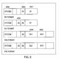
- FIG. 2illustrates exemplary instruction formats.
- FIG. 3illustrates components of an exemplary processor.
- FIG. 4illustrates exemplary same line detection logic.
- Embodiments of the inventionprovide a method and system to detect when multiple requests are possibly to the same cache line without comparing the final results of the generated address when there is an address sliced directory conflict.
- the detectionis based on fields in the instruction text of the two instructions.
- the instruction formatsare described in the IBM Z/Architecture Principles of Operation, Publication SA22-7832-00, pages 5-2 to 5-7. Additional formats are described in U.S. patent application entitled “Long Displacement Instruction Formats”, Ser. No. 10/403,417. Once detected this information is signaled to the cache to allow the cache to use information from the single directory lookup to be used to read two different interleaves for the same line simultaneously.
- An exemplary processor for implementing embodiments of the inventionhas a six stage pipeline that is capable of decoding and executing multiple instructions in a single cycle.
- the processorhas a six stage pipeline including an instruction decode 100 , address generation 101 , cache directory and interleave read 102 , data validation and return 103 , execution 104 , and put away 105 .
- the processorcan simultaneously decode two instructions during the first cycle of the pipeline.
- the processorcan simultaneously generate two addresses during the second cycle of the pipeline.
- the methods and systems disclosed hereinalso permit simultaneous same line access even when there is address sliced directory conflict.
- Embodiments of the inventionallow for multiple (e.g., two) instructions to execute together during the execution cycle 104 which return data together during the cache return cycle 103 for which the data for both instructions are in different interleaves of the cache for the same cache line.
- both interleaves for the same lineare read during the cache read cycle 102 .
- the addresses for the two requestsare generated during the address generation cycle 101 . The time required to generate this address does not permit the ability to compare the two addresses to see if they are for the same cache line.
- the processorimplements a detection method during the decode cycle 100 by examining parts of the instruction text of the two instructions. If both instructions need to address the same cache line, the processor access will read two interleaves for the same line based only on the information from the single directory lookup.
- FIG. 2illustrates exemplary instruction formats and associated fields.
- Each instructionincludes an opcode field 206 identifying the instruction and a base register field 200 .
- RX format and RXE format instructionsinclude an index field 203 .
- a displacement fieldmay be a one-part 201 as shown in the RS and RX format.
- the RSE and RXE format instructionshave a two-part displacement field divided into a low order part 204 and a high order part 205 .
- the processorexamines fields of the instructions to determine if both instructions need to address the same cache line.
- FIG. 3illustrates components of an exemplary processor for determining when two instructions address the same cache line.
- parallel processing pipelinesare provided for accessing the cache without incurring significant area increase by not requiring multi-ported arrays.
- Significant area increaseis avoided by splitting the cache directories (one for each processing pipeline) wherein the directories are split between the even and odd address of the cache and data fetches (odd or even) are processed by the corresponding pipeline (odd or even).
- Each processing pipelinehas access to the entire cache to allow for mismatching data fetches (odd fetch on an even pipeline or vice versa) thus two fetches to the same line can be processed at the same time.
- the instruction unitmay issue up to 2 operand requests to the data cache.
- the data cachecan process up to 2 operand requests and send up to 2 operand data to the execution unit.
- 2 processing pipelinesare interleaved by line address. Each pipeline has a directory that contains half of the data cache lines.
- the data cache arrayitself is structured as a 4-way interleave based upon the double word (a 64 bit operand) address.
- the data cache arraycan be accessed from either pipeline.
- FIG. 3depicts instruction text 1 and instruction text 2 from instructions received on two pipes.
- a first instructionhas a displacement field 302 , a base register field 301 , an index field 300 and an opcode field 303 .
- a second instructionhas a displacement field 306 , a base register field 305 , an index field 304 and an opcode field 307 .
- the base register fields 301 and 305 and index fields 300 and 304are used to read from the general purpose register (GPR) file 308 the base and index register contents.
- GPRgeneral purpose register
- these register contents with the displacement fields 302 and 306are used in address generation units 310 and 311 to form addresses 314 and 315 for each operand. These are sent to the cache 312 during the address generation cycle 101 .
- the information from the same line detection unit 309indicates to cache 312 that these are for the same line as shown by same line signal 313 .
- the same line signal 313either enables or disables the simultaneous access to different interleaves of the same cache line.
- the same line detection unit 309is described in further detail with reference to FIG. 4 .
- the cache 312 during the cache read cycle 102will read two interleaves for the same line based only on the information from the single directory lookup that did not have a cache directory address conflict. This allows the cache to return data for both requests during the return cycle 103 , execution of both instructions during the execution cycle 104 and result put-away for both instructions during the put-away cycle 105 .
- FIG. 4is a block diagram of an exemplary same line detection unit 309 .
- Same line detection unit 309includes index field logic 400 , base register field logic 401 , displacement field logic 402 and opcode field logic 403 .
- a same line detector 404receives an output from logic devices 400 – 403 to detect whether the same line of cache is addressed by both instructions.
- the opcode fields 303 and 307are examined by opcode field logic 403 to determine if the instruction has an index register field 203 and the length of the displacement field which may be a one-part field 201 or a two-part field 204 and 205 .
- the presence or absence of an index register field and the length of the displacement fieldis provided to the same line detector 404 .
- the base register fields 301 and 305are checked for equality at base register field logic 401 .
- the result of the comparisonis provided to the same line detector 404 . If the base register fields 301 and 305 are not equal, then the two instructions are not requesting the same line of cache. Thus, the same line signal 313 will not enable a simultaneous same line access.
- Portions of the displacement fields 302 and 306 used to generate the cache line addressare checked for equality at displacement field logic 402 .
- the one part displacement field 201 and the lower part 204 of the two-part displacement fieldare checked for equality at displacement field logic 402 .
- the high order part 205 of the displacement fields 302 and 306when it exists, is checked to see if it is zero in each instruction or equal between the two instructions at displacement field logic 402 .
- both displacement fieldshave the same format (i.e., both one-part or both two-part)
- these portionsare compared for equality and if not equal, the then the two instructions are not requesting the same line of cache.
- the same line signal 313will not enable a simultaneous same line access.
- the displacement fieldshave different formats (i.e., one is one-part and the other is two-part)
- the lower partmust equal the one-part displacement field and the upper part must be zero for an equality to be detected. Otherwise, the two instructions are not requesting the same line of cache and the same line signal 313 will not enable a simultaneous same line access.
- index fields 300 and 304if present, from each instruction are checked to see if they are the same at index field logic 400 . If both instructions have an index field, these fields are compared. If not equal, then the two instructions are not requesting the same line of cache and the same line signal 313 will not enable a simultaneous same line access.
- one instructionincludes an index field and the other instruction does not, then the present index field is checked to determine is it is zero. If not zero, the two instructions are not requesting the same line of cache and the same line signal 313 will not enable a simultaneous same line access. If the sole index field has a value of zero, then the index field logic 400 does not prevent same line access. If neither instruction includes an index field (e.g., instruction formats RS and RSE in FIG. 2 ), then the index field logic 400 does not prevent simultaneous same line access.
- an index fielde.g., instruction formats RS and RSE in FIG. 2
- index field logic 400base register field logic 401 and displacement field logic 402 , along with the information on what fields exist from opcode field logic 403 are used by same line detector 404 to determine if the addresses for the two instructions that were decoded in the decode cycle 100 are likely from the same cache line. If so, the same line detection unit 309 enables same line access to the cache through same line signal 313 . The processor access will read two interleaves for the same line based only on the information from the single directory lookup.
Landscapes
- Engineering & Computer Science (AREA)
- Theoretical Computer Science (AREA)
- Physics & Mathematics (AREA)
- General Engineering & Computer Science (AREA)
- General Physics & Mathematics (AREA)
- Software Systems (AREA)
- Memory System Of A Hierarchy Structure (AREA)
- Advance Control (AREA)
Abstract
Description
Claims (18)
Priority Applications (3)
| Application Number | Priority Date | Filing Date | Title |
|---|---|---|---|
| US10/435,967US7035986B2 (en) | 2003-05-12 | 2003-05-12 | System and method for simultaneous access of the same line in cache storage |
| PCT/GB2004/001705WO2004099974A1 (en) | 2003-05-12 | 2004-04-19 | Simultaneous access of the same line in cache storage |
| TW093112301ATWI259364B (en) | 2003-05-12 | 2004-04-30 | System and method for simultaneous access of the same line in cache storage |
Applications Claiming Priority (1)
| Application Number | Priority Date | Filing Date | Title |
|---|---|---|---|
| US10/435,967US7035986B2 (en) | 2003-05-12 | 2003-05-12 | System and method for simultaneous access of the same line in cache storage |
Publications (2)
| Publication Number | Publication Date |
|---|---|
| US20040230760A1 US20040230760A1 (en) | 2004-11-18 |
| US7035986B2true US7035986B2 (en) | 2006-04-25 |
Family
ID=33417054
Family Applications (1)
| Application Number | Title | Priority Date | Filing Date |
|---|---|---|---|
| US10/435,967Expired - LifetimeUS7035986B2 (en) | 2003-05-12 | 2003-05-12 | System and method for simultaneous access of the same line in cache storage |
Country Status (3)
| Country | Link |
|---|---|
| US (1) | US7035986B2 (en) |
| TW (1) | TWI259364B (en) |
| WO (1) | WO2004099974A1 (en) |
Cited By (2)
| Publication number | Priority date | Publication date | Assignee | Title |
|---|---|---|---|---|
| US20060236036A1 (en)* | 2005-04-13 | 2006-10-19 | Gschwind Michael K | Method and apparatus for predictive scheduling of memory accesses based on reference locality |
| US20090204766A1 (en)* | 2008-02-12 | 2009-08-13 | International Business Machines Corporation | Method, system, and computer program product for handling errors in a cache without processor core recovery |
Families Citing this family (17)
| Publication number | Priority date | Publication date | Assignee | Title |
|---|---|---|---|---|
| TWI379195B (en)* | 2009-04-13 | 2012-12-11 | Realtek Semiconductor Corp | Method and device for accessing memory and central processing unit using the same |
| US9715383B2 (en) | 2012-03-15 | 2017-07-25 | International Business Machines Corporation | Vector find element equal instruction |
| US9710266B2 (en) | 2012-03-15 | 2017-07-18 | International Business Machines Corporation | Instruction to compute the distance to a specified memory boundary |
| US9280347B2 (en) | 2012-03-15 | 2016-03-08 | International Business Machines Corporation | Transforming non-contiguous instruction specifiers to contiguous instruction specifiers |
| US9268566B2 (en) | 2012-03-15 | 2016-02-23 | International Business Machines Corporation | Character data match determination by loading registers at most up to memory block boundary and comparing |
| US9459864B2 (en) | 2012-03-15 | 2016-10-04 | International Business Machines Corporation | Vector string range compare |
| US9459867B2 (en) | 2012-03-15 | 2016-10-04 | International Business Machines Corporation | Instruction to load data up to a specified memory boundary indicated by the instruction |
| US9454367B2 (en) | 2012-03-15 | 2016-09-27 | International Business Machines Corporation | Finding the length of a set of character data having a termination character |
| US9459868B2 (en) | 2012-03-15 | 2016-10-04 | International Business Machines Corporation | Instruction to load data up to a dynamically determined memory boundary |
| US9454366B2 (en) | 2012-03-15 | 2016-09-27 | International Business Machines Corporation | Copying character data having a termination character from one memory location to another |
| US9588762B2 (en) | 2012-03-15 | 2017-03-07 | International Business Machines Corporation | Vector find element not equal instruction |
| US20140085320A1 (en)* | 2012-09-27 | 2014-03-27 | Apple Inc. | Efficient processing of access requests for a shared resource |
| US10311229B1 (en)* | 2015-05-18 | 2019-06-04 | Amazon Technologies, Inc. | Mitigating timing side-channel attacks by obscuring alternatives in code |
| US10868665B1 (en)* | 2015-05-18 | 2020-12-15 | Amazon Technologies, Inc. | Mitigating timing side-channel attacks by obscuring accesses to sensitive data |
| US10235297B2 (en)* | 2015-11-04 | 2019-03-19 | International Business Machines Corporation | Mechanism for creating friendly transactions with credentials |
| US10270773B2 (en)* | 2015-11-04 | 2019-04-23 | International Business Machines Corporation | Mechanism for creating friendly transactions with credentials |
| CN111829533B (en)* | 2019-04-18 | 2022-09-09 | 广州市百果园信息技术有限公司 | Data detection method, device, equipment and storage medium |
Citations (5)
| Publication number | Priority date | Publication date | Assignee | Title |
|---|---|---|---|---|
| US5640534A (en) | 1994-10-05 | 1997-06-17 | International Business Machines Corporation | Method and system for concurrent access in a data cache array utilizing multiple match line selection paths |
| US5805855A (en) | 1994-10-05 | 1998-09-08 | International Business Machines Corporation | Data cache array having multiple content addressable fields per cache line |
| US5890217A (en)* | 1995-03-20 | 1999-03-30 | Fujitsu Limited | Coherence apparatus for cache of multiprocessor |
| US6202128B1 (en) | 1998-03-11 | 2001-03-13 | International Business Machines Corporation | Method and system for pre-fetch cache interrogation using snoop port |
| US6493800B1 (en)* | 1999-03-31 | 2002-12-10 | International Business Machines Corporation | Method and system for dynamically partitioning a shared cache |
Family Cites Families (2)
| Publication number | Priority date | Publication date | Assignee | Title |
|---|---|---|---|---|
| US6463514B1 (en)* | 1998-02-18 | 2002-10-08 | International Business Machines Corporation | Method to arbitrate for a cache block |
| GB2365582A (en)* | 2000-02-18 | 2002-02-20 | Hewlett Packard Co | High bandwidth cache |
- 2003
- 2003-05-12USUS10/435,967patent/US7035986B2/ennot_activeExpired - Lifetime
- 2004
- 2004-04-19WOPCT/GB2004/001705patent/WO2004099974A1/enactiveApplication Filing
- 2004-04-30TWTW093112301Apatent/TWI259364B/enactive
Patent Citations (5)
| Publication number | Priority date | Publication date | Assignee | Title |
|---|---|---|---|---|
| US5640534A (en) | 1994-10-05 | 1997-06-17 | International Business Machines Corporation | Method and system for concurrent access in a data cache array utilizing multiple match line selection paths |
| US5805855A (en) | 1994-10-05 | 1998-09-08 | International Business Machines Corporation | Data cache array having multiple content addressable fields per cache line |
| US5890217A (en)* | 1995-03-20 | 1999-03-30 | Fujitsu Limited | Coherence apparatus for cache of multiprocessor |
| US6202128B1 (en) | 1998-03-11 | 2001-03-13 | International Business Machines Corporation | Method and system for pre-fetch cache interrogation using snoop port |
| US6493800B1 (en)* | 1999-03-31 | 2002-12-10 | International Business Machines Corporation | Method and system for dynamically partitioning a shared cache |
Cited By (3)
| Publication number | Priority date | Publication date | Assignee | Title |
|---|---|---|---|---|
| US20060236036A1 (en)* | 2005-04-13 | 2006-10-19 | Gschwind Michael K | Method and apparatus for predictive scheduling of memory accesses based on reference locality |
| US20090204766A1 (en)* | 2008-02-12 | 2009-08-13 | International Business Machines Corporation | Method, system, and computer program product for handling errors in a cache without processor core recovery |
| US7987384B2 (en)* | 2008-02-12 | 2011-07-26 | International Business Machines Corporation | Method, system, and computer program product for handling errors in a cache without processor core recovery |
Also Published As
| Publication number | Publication date |
|---|---|
| TWI259364B (en) | 2006-08-01 |
| US20040230760A1 (en) | 2004-11-18 |
| WO2004099974A1 (en) | 2004-11-18 |
| TW200506610A (en) | 2005-02-16 |
Similar Documents
| Publication | Publication Date | Title |
|---|---|---|
| US7035986B2 (en) | System and method for simultaneous access of the same line in cache storage | |
| US5519842A (en) | Method and apparatus for performing unaligned little endian and big endian data accesses in a processing system | |
| US5509119A (en) | Fast comparison method and apparatus for error corrected cache tags | |
| US8127078B2 (en) | High performance unaligned cache access | |
| JP4045062B2 (en) | Method, processor, and system for executing load instructions | |
| US7882332B1 (en) | Memory mapped register file | |
| US5778407A (en) | Methods and apparatus for determining operating characteristics of a memory element based on its physical location | |
| US5875201A (en) | Second level cache having instruction cache parity error control | |
| US5893930A (en) | Predictive translation of a data address utilizing sets of associative entries stored consecutively in a translation lookaside buffer | |
| US6266768B1 (en) | System and method for permitting out-of-order execution of load instructions | |
| JPS604494B2 (en) | cash storage system | |
| US4831622A (en) | Apparatus for forcing a reload from main memory upon cache memory error | |
| US20050273669A1 (en) | Cache entry error-correcting code (ECC) based at least on cache entry data and memory address | |
| US6571316B1 (en) | Cache memory array for multiple address spaces | |
| US5893146A (en) | Cache structure having a reduced tag comparison to enable data transfer from said cache | |
| US8707014B2 (en) | Arithmetic processing unit and control method for cache hit check instruction execution | |
| US7039762B2 (en) | Parallel cache interleave accesses with address-sliced directories | |
| JPH0512126A (en) | Virtual computer address translation device and address translation method | |
| JP4459628B2 (en) | Using context identifiers in cache memory | |
| US6477635B1 (en) | Data processing system including load/store unit having a real address tag array and method for correcting effective address aliasing | |
| US6990556B2 (en) | System and method for simultaneous access of the same doubleword in cache storage | |
| US6640293B1 (en) | Apparatus and method of utilizing Alias Hit signals to detect errors within the real address tag arrays | |
| US5414821A (en) | Method of and apparatus for rapidly loading addressing environment by checking and loading multiple registers using a specialized instruction | |
| US20030018936A1 (en) | High integrity cache directory | |
| US6704820B1 (en) | Unified cache port consolidation |
Legal Events
| Date | Code | Title | Description |
|---|---|---|---|
| AS | Assignment | Owner name:INTERNATIONAL BUSINESS MACHINES CORPORATION, NEW Y Free format text:ASSIGNMENT OF ASSIGNORS INTEREST;ASSIGNORS:CHECK, MARK A.;NAVARRO, JENNIFER A.;SHUM, CHUNG-LUNG K.;AND OTHERS;REEL/FRAME:014068/0452;SIGNING DATES FROM 20030508 TO 20030509 | |
| FEPP | Fee payment procedure | Free format text:PAYOR NUMBER ASSIGNED (ORIGINAL EVENT CODE: ASPN); ENTITY STATUS OF PATENT OWNER: LARGE ENTITY | |
| STCF | Information on status: patent grant | Free format text:PATENTED CASE | |
| FPAY | Fee payment | Year of fee payment:4 | |
| REMI | Maintenance fee reminder mailed | ||
| AS | Assignment | Owner name:TWITTER, INC., CALIFORNIA Free format text:ASSIGNMENT OF ASSIGNORS INTEREST;ASSIGNOR:INTERNATIONAL BUSINESS MACHINES CORPORATION;REEL/FRAME:032075/0404 Effective date:20131230 | |
| FPAY | Fee payment | Year of fee payment:8 | |
| SULP | Surcharge for late payment | Year of fee payment:7 | |
| FEPP | Fee payment procedure | Free format text:MAINTENANCE FEE REMINDER MAILED (ORIGINAL EVENT CODE: REM.) | |
| FEPP | Fee payment procedure | Free format text:11.5 YR SURCHARGE- LATE PMT W/IN 6 MO, LARGE ENTITY (ORIGINAL EVENT CODE: M1556) | |
| MAFP | Maintenance fee payment | Free format text:PAYMENT OF MAINTENANCE FEE, 12TH YEAR, LARGE ENTITY (ORIGINAL EVENT CODE: M1553) Year of fee payment:12 | |
| AS | Assignment | Owner name:MORGAN STANLEY SENIOR FUNDING, INC., MARYLAND Free format text:SECURITY INTEREST;ASSIGNOR:TWITTER, INC.;REEL/FRAME:062079/0677 Effective date:20221027 Owner name:MORGAN STANLEY SENIOR FUNDING, INC., MARYLAND Free format text:SECURITY INTEREST;ASSIGNOR:TWITTER, INC.;REEL/FRAME:061804/0086 Effective date:20221027 Owner name:MORGAN STANLEY SENIOR FUNDING, INC., MARYLAND Free format text:SECURITY INTEREST;ASSIGNOR:TWITTER, INC.;REEL/FRAME:061804/0001 Effective date:20221027 | |
| AS | Assignment | Owner name:X CORP. (F/K/A TWITTER, INC.), TEXAS Free format text:RELEASE BY SECURED PARTY;ASSIGNOR:MORGAN STANLEY SENIOR FUNDING, INC.;REEL/FRAME:070670/0857 Effective date:20250220 | |
| AS | Assignment | Owner name:X CORP. (F/K/A TWITTER, INC.), TEXAS Free format text:RELEASE BY SECURED PARTY;ASSIGNOR:MORGAN STANLEY SENIOR FUNDING, INC., AS COLLATERAL AGENT;REEL/FRAME:071127/0240 Effective date:20250429 |