US7034769B2 - Modified printed dipole antennas for wireless multi-band communication systems - Google Patents
Modified printed dipole antennas for wireless multi-band communication systemsDownload PDFInfo
- Publication number
- US7034769B2 US7034769B2US10/718,568US71856803AUS7034769B2US 7034769 B2US7034769 B2US 7034769B2US 71856803 AUS71856803 AUS 71856803AUS 7034769 B2US7034769 B2US 7034769B2
- Authority
- US
- United States
- Prior art keywords
- conductive
- shape
- antenna according
- dielectric layer
- conductive element
- Prior art date
- Legal status (The legal status is an assumption and is not a legal conclusion. Google has not performed a legal analysis and makes no representation as to the accuracy of the status listed.)
- Expired - Lifetime, expires
Links
Images


Classifications
- H—ELECTRICITY
- H01—ELECTRIC ELEMENTS
- H01Q—ANTENNAS, i.e. RADIO AERIALS
- H01Q9/00—Electrically-short antennas having dimensions not more than twice the operating wavelength and consisting of conductive active radiating elements
- H01Q9/04—Resonant antennas
- H01Q9/16—Resonant antennas with feed intermediate between the extremities of the antenna, e.g. centre-fed dipole
- H01Q9/28—Conical, cylindrical, cage, strip, gauze, or like elements having an extended radiating surface; Elements comprising two conical surfaces having collinear axes and adjacent apices and fed by two-conductor transmission lines
- H01Q9/285—Planar dipole
- H—ELECTRICITY
- H01—ELECTRIC ELEMENTS
- H01Q—ANTENNAS, i.e. RADIO AERIALS
- H01Q1/00—Details of, or arrangements associated with, antennas
- H01Q1/36—Structural form of radiating elements, e.g. cone, spiral, umbrella; Particular materials used therewith
- H01Q1/38—Structural form of radiating elements, e.g. cone, spiral, umbrella; Particular materials used therewith formed by a conductive layer on an insulating support
- H—ELECTRICITY
- H01—ELECTRIC ELEMENTS
- H01Q—ANTENNAS, i.e. RADIO AERIALS
- H01Q21/00—Antenna arrays or systems
- H01Q21/30—Combinations of separate antenna units operating in different wavebands and connected to a common feeder system
- H—ELECTRICITY
- H01—ELECTRIC ELEMENTS
- H01Q—ANTENNAS, i.e. RADIO AERIALS
- H01Q9/00—Electrically-short antennas having dimensions not more than twice the operating wavelength and consisting of conductive active radiating elements
- H01Q9/04—Resonant antennas
- H01Q9/16—Resonant antennas with feed intermediate between the extremities of the antenna, e.g. centre-fed dipole
- H01Q9/28—Conical, cylindrical, cage, strip, gauze, or like elements having an extended radiating surface; Elements comprising two conical surfaces having collinear axes and adjacent apices and fed by two-conductor transmission lines
Definitions
- the present disclosurerelates to an antenna for wireless communication devices and systems and, more specifically, to printed dipole antennas for communication for wireless multi-band communication systems.
- Wireless communication devices and systemsare generally hand held or are part of portable laptop computers. Thus, the antenna must be of very small dimensions in order to fit the appropriate device.
- the systemis used for general communication, as well as for wireless local area network (WLAN) systems.
- Dipole antennashave been used in these systems because they are small and can be tuned to the appropriate frequency.
- the shape of the printed dipoleis generally a narrow, rectangular strip with a width less than 0.05 ⁇ 0 and a total length less than 0.5 ⁇ 0 .
- the theoretical gain of the isotrope dipoleis generally 2.5 dB and for a double dipole is less than or equal to 3 dB.
- One popular printed dipole antennais the planar inverted-F antenna (PIFA).
- the present disclosureis a dipole antenna for a wireless communication device. It includes a first conductive element superimposed on a portion of and separated from a second conductive element by a first dielectric layer. A first conductive via connects the first and second conductive elements through the first dielectric layer.
- the second conductive elementis generally U-shaped.
- the second conductive elementincludes a plurality of spaced conductive strips extending transverse from adjacent ends of the legs of the U-shape. Each strip is dimensioned for a different center frequency ⁇ 0 .
- the first conductive elementmay be L-shaped and one of the legs of the L-shape being superimposed on one of the legs of the U-shape.
- the first conductive viaconnects the other leg of the L-shape to the other leg of the U-shape.
- the first and second conductive elementsare each planar.
- the stripshave a width of less than 0.05 ⁇ 0 and a length of less than 0.5 ⁇ 0 .
- the antennamay be omni-directional or uni-dimensional. If it is uni-dimensional, it includes a ground plane conductor superimposed and separated from the second conductive element by a second dielectric layer. A third conductive element is superimposed and separated from the strips of the second conductive element by the first dielectric layer. A second conductive via connects the third conductive element to the ground conductor through the dielectric layers.
- the first and third conductive elementsmay be co-planar.
- the third conductive elementincludes a plurality of fingers superimposed on a portion of lateral edges of each of the strips.
- FIG. 1is a perspective, diagrammatic view of an omni-directional, quad-band dipole antenna incorporating the principles of the present invention.
- FIG. 2Ais a plane view of the dipole conductive layers of FIG. 1 .
- FIG. 2Bis a six-band modification of the dipole conductive layer of FIG. 2A .
- FIG. 3is a plane view of the antenna of FIG. 1 .
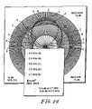
- FIG. 4is a directional diagram of the antenna of FIG. 1 .
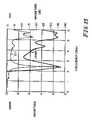
- FIG. 5is a graph of the directional gain of two of the tuned frequencies.
- FIG. 6is a graph of the frequency versus voltage standing wave ratio (VSWR) and the gain of S 11 .
- FIG. 7Ais a graph showing the effects of changing the feed point or via on the characteristics of the dipole antenna of FIG. 1 , as illustrated in FIG. 7B .
- FIG. 8is a graph showing the effects of changing the width of the slot S of the dipole of FIG. 1 .
- FIG. 9is a graph showing the effects for a 2-, 3- and 4-strip dipole of FIG. 1 .
- FIG. 10Ais a graph showing the effects of changing the width of the dipole of FIG. 1 , as illustrated in FIG. 10B .
- FIG. 11is a perspective, diagrammatic view of a directional dipole antenna incorporating the principles of the present invention.
- FIG. 12is a plane top view of the antenna of FIG. 11 .
- FIG. 13is a bottom view of the antenna of FIG. 11 .
- FIG. 14is a graph of the directional gain of the antenna of FIG. 11 for five frequencies.
- FIG. 15is a graph of frequency versus VSWR and S 11 of the antenna of FIG. 11 .
- FIG. 16Ais a graph showing the effects of changing the feed point or via 40 for the feed positions illustrated in FIG. 16B for the dipole antenna of FIG. 11 .
- FIG. 17is a graph showing the effects of changing the width of slot S for the dipole antenna of FIG. 11 .
- FIG. 18Ais a graph showing the effects of changing the width of the dipole, as illustrated in FIG. 18B , of the antenna of FIG. 11 .
- FIG. 19Ais a graph of the second frequency showing the effect of changing the length of the directive dipole, as illustrated in FIG. 19B , of the dipole antenna of FIG. 11 .
- the present antenna of a systemwill be described with respect to WLAN dual frequency bands of, e.g., approximately 2.4 GHz and 5.2 GHz, the present antenna can be designed for operation in any of the frequency bands for portable, wireless communication devices. These could include GPS (1575 MHz), cellular telephones (824–970 MHz and 860–890 MHz), some PCS devices (1710–1810 MHz, 1750–1870 MHz and 1850–1990 MHz), cordless telephones (902–928 MHz) or Blue Tooth Specification 2.4–2.5 GHS frequency ranges.
- the antenna system 10 of FIGS. 1 , 2 A and 3includes a dielectric substrate 12 with cover layers 14 , 16 .
- Printed on the substrate 12is a first conductive layer 20 , which is a micro-strip line, and on the opposite side is a split dipole conductive layer 30 .
- the first conductive layer 20is generally L-shaped having legs 22 , 24 .
- the second conductive layer 30includes a generally U-shaped strip balloon line portion 32 having a bight 31 and a pair of separated legs 33 . Extending transverse and adjacent the ends of the legs 33 are a plurality of strips 35 , 37 , 34 , 36 .
- Leg 22 of the first conductive layer 20is superimposed upon one of the legs 33 of the second conductive layer 30 with the other leg 24 extending transverse a pair of legs 33 .
- a conductive via 40connects the end of leg 24 to one of the legs 33 through the dielectric substrate 12 .
- Terminal 26 at the other end of leg 22 of the first conductive layer 20receives the drive for the antenna 10 .
- the four strips 34 , 36 , 35 and 37are each uniquely dimensioned so as to be tuned to or receive different frequency signals. They are each dimensioned such that the strip has a width less than 0.05 ⁇ 0 and a total length of less than 0.5 ⁇ 0.
- FIG. 2Bshows a modification of FIG. 2A , including six strips 35 , 37 , 39 , 34 , 36 , 38 each extending from an adjacent end of the legs 33 of the second conductive layer 30 . This allows tuning and reception to six different frequency bands.
- the strips of both embodimentsare generally parallel to each other.
- the dielectric substrate 12may be a printed circuit board, a fiberglass or a flexible film substrate made of polyimide. Covers 14 , 16 may be additional, applied dielectric layers or may be hollow casing structures. Preferably, the conductive layers 20 , 30 are printed on the dielectric substrate 12 .
- the frequenciesmay be in the range of, for example, 2.4–2.487, 5.15–5.25, 2.25–5.35 and 5.74–5.825 GHz.
- the directional gainis illustrated in FIG. 5 for two of the frequencies 2.4 GHz (Graph A) and 5.6 GHz (Graph B).
- a maximal gain at 90 degreesis 5.45 dB at 2.4 GHz and 6.19 dB at 5.6 GHz.
- VSWR and the magnitude S 11are illustrated in FIG. 6 .
- VSWRis below 2 at the 2.4 GHz and the 5.6 GHz frequency bands. The bands from 5.15–5.827 merge at the 5.6 GHz frequency.
- the height h of the dielectric substrate 12will vary depending upon the permeability or dielectric constant of the layer.
- the narrow, rectangular strips 34 , 36 , 35 , 37 of the appropriate dimensionincreases the total gain by reducing the surface waves and loss in the conductive layer.
- the number of conductive stripsalso effects the frequency sub-band.
- the position of the via 40 and the slot S between the legs 33 of the U-shaped sub-conductor 32effect the antenna performance related to the gain “distributions” in the frequency bands.
- a width of slot dimensions S and the location of the via 40are selected so as to have approximately the same gain in all of the frequency bands of the strips 34 , 36 , 35 , 37 .
- the maximum theoretical gain obtainedare above 4 dB and are 5.7 dB at 2.4 GHz and 7.5 dB at 5.4 GHz.
- FIG. 7Ais a graph for the various positions of the feed point fp or via 40 and the effect on VSWR and S 11 .
- the center feed point fp 1corresponds to the results of FIG. 6 .
- the change of the feed point fphas a small effect in gain, it has a greater effect in shifting the ⁇ 0 at the second frequency band in the 5 GHz range.
- FIG. 8shows the effect of changing the slot width from 1 mm to 3 mm to 5 mm.
- the 3 mm slot widthcorresponds to FIG. 6 .
- S 11is ⁇ 21 dB at 2.5 GHz and ⁇ 16 dB at 5.3 GHz.
- S 11is ⁇ 14 dB at 2.5 GHz and ⁇ 25 dB at 5.23 GHz.
- S 11is approximately equal to ⁇ 13 dB at 2.5 GHz and at 5.3 GHz.
- FIG. 6corresponds to a 15 mm length. Also, changing the distance between the legs 34 , 35 , 36 , 37 to between 1 mm, 2 mm and 4 mm also has very little effect on VSWR and the gain at S 11 . Two millimeters of separation is reflected in FIG. 6 . The difference in gain between the 2 mm and the 4 mm spacing was approximately 2 dB.
- FIG. 9shows the response of 2, 3 and 4 dipole strips.
- the 10 mm widthis one large band at a VSWR below two extending from 1.65 to 5.16 GHz and having a gain at 2.2 GHz of ⁇ 34 dB to a gain at 4.9 GHz of ⁇ 11 dB.
- FIGS. 7 through 9A directional or unidirectional dipole antenna incorporating the principles of the present invention is illustrated in FIGS. 7 through 9 . Those elements having the same structure, function and purpose as that of the omni-directional antenna of FIG. 1 have the same numbers.
- the antenna 11 of FIGS. 11 through 13includes, in addition to the first conductive layer 20 on a first surface of the dielectric substrate 12 and a second conductive dipole 30 on the opposite surface of the dielectric substrate 12 , a ground conductive layer 60 separated from the second conductive layer 30 by the lower dielectric layer 16 .
- a third conductive element 50is provided on the same surface of the dielectric substrate 12 as the first conductive element 20 .
- the third conductive element 50is a directive dipole. It includes a center strip 51 having a pair of end portions 53 . This is generally a barbell-shaped conductive element. It is superimposed over the strips 34 , 36 , 35 , 37 of the second conductive layer 30 . It is connected to the ground layer 60 by a via 42 extending through the dielectric substrate 12 and dielectric layer 16 .
- the directive dipole 50includes a plurality of fingers superimposed on a portion of the edges of each of the strips 34 , 36 , 35 , 37 . As illustrated, the end strips 52 , 58 are superimposed and extend laterally beyond the lateral edges of strips 34 , 36 , 35 , 37 .
- the inner fingers 54 , 56are adjacent to the inner edge of strips 34 , 36 , 35 , 37 and do not extend laterally therebeyond.
- the permeability or dielectric constant of the dielectric substrate 12is greater than the permeability or dielectric constant of the dielectric layer 16 .
- the thickness h 1 of the dielectric substrate 12is substantially less than the thickness h 2 of the dielectric layer 16 .
- the dielectric substrate 12is at least half of the thickness of the dielectric layer 16 .
- the polygonal perimeter of the end portion 53 of the dipole directive 50has a similar shape of the PEAN03 fractal shape directive dipole. It should also be noted that the profile of the antenna 12 gives the appearance of a double planar inverted-F antenna (PIFA).
- PIFAplanar inverted-F antenna
- FIG. 14is a graph of the directional gain of antenna 12
- FIG. 15shows a graph for the VSWR and the gain S 11 .
- Five frequenciesare illustrated in FIG. 10 .
- the maximum gainare above 7 dB and are 8.29 dB at 2.5 GHz and 10.5 dB at 5.7 GHz.
- the VSWR in FIG. 15is for at least two frequency bands that are below 2.
- FIGS. 16A and 16Bshow the effect of the feed point fp or via 40 .
- Feed point zerois similar to that shown in FIG. 15 .
- FIG. 17shows the effect of the slot width S for 1 mm, 3 mm and 5 mm. The 3 mm width corresponds generally to that of FIG. 15 .
- FIGS. 18A and 18Bshow the effect of the dipole strip width SW for widths of 6 mm, 8 mm and 10 mm. The 6 mm width corresponds to that of FIG. 15 .
- FIGS. 19A and 19Bshow the effect of the length SDL of portion 51 of the directive dipole 50 on the second frequency in the 5 GHz range. The 8 mm width corresponds generally to that of FIG. 15 .
- via holes around the dipole through the insulated layer 12may be provided. These via holes would provide pseudo-photonic crystals. This would increase the total gain by reducing the surface waves and the radiation in the dielectric material. This is true of both antennas.
Landscapes
- Details Of Aerials (AREA)
- Variable-Direction Aerials And Aerial Arrays (AREA)
- Mobile Radio Communication Systems (AREA)
- Transceivers (AREA)
- Developing Agents For Electrophotography (AREA)
- Support Of Aerials (AREA)
Abstract
Description
Claims (19)
Priority Applications (12)
| Application Number | Priority Date | Filing Date | Title |
|---|---|---|---|
| US10/718,568US7034769B2 (en) | 2003-11-24 | 2003-11-24 | Modified printed dipole antennas for wireless multi-band communication systems |
| US10/859,169US7095382B2 (en) | 2003-11-24 | 2004-06-03 | Modified printed dipole antennas for wireless multi-band communications systems |
| TW093132540ATW200525819A (en) | 2003-11-24 | 2004-10-27 | Modified printed dipole antennas for wireless multi-band communication systems |
| EP04816981AEP1687867B1 (en) | 2003-11-24 | 2004-11-22 | Modified printed dipole antennas for wireless multi-band communication systems |
| CN200480034696.4ACN1886865B (en) | 2003-11-24 | 2004-11-22 | Improved printed dipole antenna for wireless multi-band communication system |
| KR1020067010057AKR101090592B1 (en) | 2003-11-24 | 2004-11-22 | Modified printed dipole antenna for wireless multi-band communication systems |
| JP2006541660AJP2007534226A (en) | 2003-11-24 | 2004-11-22 | Improved printed dipole antenna for wireless multiband communication systems |
| DE602004017495TDE602004017495D1 (en) | 2003-11-24 | 2004-11-22 | MODIFIED PRINTED DIPOLANTS FOR WIRELESS MULTI-BAND COMMUNICATION SYSTEMS |
| PCT/US2004/039342WO2005053092A1 (en) | 2003-11-24 | 2004-11-22 | Modified printed dipole antennas for wireless multi-band communication systems |
| AT04816981TATE412990T1 (en) | 2003-11-24 | 2004-11-22 | MODIFIED PRINTED DIPOL ANTENNAS FOR MULTI-BAND WIRELESS COMMUNICATION SYSTEMS |
| CN201410329323.5ACN104124521B (en) | 2003-11-24 | 2004-11-22 | Improved printed dipole antenna for wireless multi-band communication system |
| US11/413,589US20060208956A1 (en) | 2003-11-24 | 2006-04-28 | Modified printed dipole antennas for wireless multi-band communication systems |
Applications Claiming Priority (1)
| Application Number | Priority Date | Filing Date | Title |
|---|---|---|---|
| US10/718,568US7034769B2 (en) | 2003-11-24 | 2003-11-24 | Modified printed dipole antennas for wireless multi-band communication systems |
Related Child Applications (1)
| Application Number | Title | Priority Date | Filing Date |
|---|---|---|---|
| US10/859,169Continuation-In-PartUS7095382B2 (en) | 2003-11-24 | 2004-06-03 | Modified printed dipole antennas for wireless multi-band communications systems |
Publications (2)
| Publication Number | Publication Date |
|---|---|
| US20050110696A1 US20050110696A1 (en) | 2005-05-26 |
| US7034769B2true US7034769B2 (en) | 2006-04-25 |
Family
ID=34591117
Family Applications (1)
| Application Number | Title | Priority Date | Filing Date |
|---|---|---|---|
| US10/718,568Expired - LifetimeUS7034769B2 (en) | 2003-11-24 | 2003-11-24 | Modified printed dipole antennas for wireless multi-band communication systems |
Country Status (9)
| Country | Link |
|---|---|
| US (1) | US7034769B2 (en) |
| EP (1) | EP1687867B1 (en) |
| JP (1) | JP2007534226A (en) |
| KR (1) | KR101090592B1 (en) |
| CN (2) | CN1886865B (en) |
| AT (1) | ATE412990T1 (en) |
| DE (1) | DE602004017495D1 (en) |
| TW (1) | TW200525819A (en) |
| WO (1) | WO2005053092A1 (en) |
Cited By (32)
| Publication number | Priority date | Publication date | Assignee | Title |
|---|---|---|---|---|
| US20050141466A1 (en)* | 2003-12-29 | 2005-06-30 | Eyal Krupka | Device, system and method for detecting and handling co-channel interference |
| US20060017622A1 (en)* | 2004-03-09 | 2006-01-26 | Centurion Wireless Technologies, Inc. | Multi-band omni directional antenna |
| US20060192720A1 (en)* | 2004-08-18 | 2006-08-31 | Ruckus Wireless, Inc. | Multiband omnidirectional planar antenna apparatus with selectable elements |
| US20060284780A1 (en)* | 2005-06-17 | 2006-12-21 | An-Chia Chen | Dual-band dipole antenna |
| US20070223599A1 (en)* | 2005-07-25 | 2007-09-27 | Sysair, Inc., A Delaware Corporation | Cellular PC modem architecture and method of operation |
| US20070247255A1 (en)* | 2004-08-18 | 2007-10-25 | Victor Shtrom | Reducing stray capacitance in antenna element switching |
| US20070252666A1 (en)* | 2006-04-28 | 2007-11-01 | Ruckus Wireless, Inc. | PIN diode network for multiband RF coupling |
| US20070293178A1 (en)* | 2006-05-23 | 2007-12-20 | Darin Milton | Antenna Control |
| US20080129640A1 (en)* | 2004-08-18 | 2008-06-05 | Ruckus Wireless, Inc. | Antennas with polarization diversity |
| US20080139136A1 (en)* | 2005-06-24 | 2008-06-12 | Victor Shtrom | Multiple-Input Multiple-Output Wireless Antennas |
| US20080136725A1 (en)* | 2004-08-18 | 2008-06-12 | Victor Shtrom | Minimized Antenna Apparatus with Selectable Elements |
| US20080158070A1 (en)* | 2006-12-29 | 2008-07-03 | Motorola, Inc. | Low interference internal antenna system for wireless devices |
| US20080291098A1 (en)* | 2005-06-24 | 2008-11-27 | William Kish | Coverage antenna apparatus with selectable horizontal and vertical polarization elements |
| US7525486B2 (en) | 2004-11-22 | 2009-04-28 | Ruckus Wireless, Inc. | Increased wireless coverage patterns |
| US20100053010A1 (en)* | 2004-08-18 | 2010-03-04 | Victor Shtrom | Antennas with Polarization Diversity |
| US20100103065A1 (en)* | 2004-08-18 | 2010-04-29 | Victor Shtrom | Dual Polarization Antenna with Increased Wireless Coverage |
| US20100103066A1 (en)* | 2004-08-18 | 2010-04-29 | Victor Shtrom | Dual Band Dual Polarization Antenna Array |
| US20100289705A1 (en)* | 2009-05-12 | 2010-11-18 | Victor Shtrom | Mountable Antenna Elements for Dual Band Antenna |
| US7893882B2 (en) | 2007-01-08 | 2011-02-22 | Ruckus Wireless, Inc. | Pattern shaping of RF emission patterns |
| US20110254738A1 (en)* | 2010-04-20 | 2011-10-20 | Chieh-Ping Chiu | Multi-band antenna |
| US8217843B2 (en) | 2009-03-13 | 2012-07-10 | Ruckus Wireless, Inc. | Adjustment of radiation patterns utilizing a position sensor |
| US8756668B2 (en) | 2012-02-09 | 2014-06-17 | Ruckus Wireless, Inc. | Dynamic PSK for hotspots |
| US8963779B2 (en) | 2010-11-08 | 2015-02-24 | Industrial Technology Research Institute | Silicon-based suspending antenna with photonic bandgap structure |
| US20150101239A1 (en)* | 2012-02-17 | 2015-04-16 | Nathaniel L. Cohen | Apparatus for using microwave energy for insect and pest control and methods thereof |
| US9019165B2 (en) | 2004-08-18 | 2015-04-28 | Ruckus Wireless, Inc. | Antenna with selectable elements for use in wireless communications |
| US9092610B2 (en) | 2012-04-04 | 2015-07-28 | Ruckus Wireless, Inc. | Key assignment for a brand |
| US9407012B2 (en) | 2010-09-21 | 2016-08-02 | Ruckus Wireless, Inc. | Antenna with dual polarization and mountable antenna elements |
| US9570799B2 (en) | 2012-09-07 | 2017-02-14 | Ruckus Wireless, Inc. | Multiband monopole antenna apparatus with ground plane aperture |
| US9634403B2 (en) | 2012-02-14 | 2017-04-25 | Ruckus Wireless, Inc. | Radio frequency emission pattern shaping |
| US9912065B2 (en)* | 2012-11-15 | 2018-03-06 | Samsung Electronics Co., Ltd. | Dipole antenna module and electronic apparatus including the same |
| US10186750B2 (en) | 2012-02-14 | 2019-01-22 | Arris Enterprises Llc | Radio frequency antenna array with spacing element |
| US10230161B2 (en) | 2013-03-15 | 2019-03-12 | Arris Enterprises Llc | Low-band reflector for dual band directional antenna |
Families Citing this family (9)
| Publication number | Priority date | Publication date | Assignee | Title |
|---|---|---|---|---|
| US7095382B2 (en)* | 2003-11-24 | 2006-08-22 | Sandbridge Technologies, Inc. | Modified printed dipole antennas for wireless multi-band communications systems |
| WO2005076962A2 (en)* | 2004-02-05 | 2005-08-25 | Amphenol-T & M Antennas | Small footprint dual band dipole antennas for wireless networking |
| CN102244317B (en)* | 2010-05-13 | 2014-01-08 | 广达电脑股份有限公司 | Multi-band antenna capable of suppressing maximum gain |
| CN203503773U (en)* | 2013-09-13 | 2014-03-26 | 中怡(苏州)科技有限公司 | Antenna structure and electronic device employing same |
| US9496623B2 (en) | 2014-11-21 | 2016-11-15 | Sony Corporation | Dual band multi-layer dipole antennas for wireless electronic devices |
| US10659175B2 (en)* | 2018-07-16 | 2020-05-19 | Litepoint Corporation | System and method for over-the-air (OTA) testing to detect faulty elements in an active array antenna of an extremely high frequency (EHF) wireless communication device |
| US11024982B2 (en) | 2019-03-21 | 2021-06-01 | Samsung Electro-Mechanics Co., Ltd. | Antenna apparatus |
| KR102529052B1 (en) | 2019-06-12 | 2023-05-03 | 삼성전기주식회사 | Antenna apparatus |
| US11515648B2 (en)* | 2021-02-04 | 2022-11-29 | Iq Group Sdn. Bhd. | Dipole antenna |
Citations (27)
| Publication number | Priority date | Publication date | Assignee | Title |
|---|---|---|---|---|
| GB1550809A (en) | 1977-04-18 | 1979-08-22 | Bendix Corp | Symmetrical balanced stripline dipole |
| US4205317A (en) | 1978-12-21 | 1980-05-27 | Louis Orenbuch | Broadband miniature antenna |
| US4438437A (en) | 1981-09-14 | 1984-03-20 | Hazeltine Corporation | Dual mode blade antenna |
| US5030962A (en) | 1981-03-11 | 1991-07-09 | The Secretary Of State For Defence In Her Britannic Majesty's Government Of The United Kingdom Of Great Britain And Northern Ireland Of Whitehall | Electromagnetic radiation sensor |
| US5532708A (en)* | 1995-03-03 | 1996-07-02 | Motorola, Inc. | Single compact dual mode antenna |
| US5949383A (en) | 1997-10-20 | 1999-09-07 | Ericsson Inc. | Compact antenna structures including baluns |
| US5986606A (en) | 1996-08-21 | 1999-11-16 | France Telecom | Planar printed-circuit antenna with short-circuited superimposed elements |
| US6072434A (en) | 1997-02-04 | 2000-06-06 | Lucent Technologies Inc. | Aperture-coupled planar inverted-F antenna |
| WO2001015270A1 (en) | 1999-08-24 | 2001-03-01 | National University Of Singapore | A compact antenna for multiple frequency operation |
| US6239765B1 (en) | 1999-02-27 | 2001-05-29 | Rangestar Wireless, Inc. | Asymmetric dipole antenna assembly |
| US6275192B1 (en) | 2000-05-31 | 2001-08-14 | Samsung Electronics Co., Ltd. | Planar antenna |
| US6300908B1 (en) | 1998-09-09 | 2001-10-09 | Centre National De La Recherche Scientifique (Cnrs) | Antenna |
| US6346921B1 (en) | 1997-12-20 | 2002-02-12 | University Of Bradford | Broadband antenna |
| US6353443B1 (en) | 1998-07-09 | 2002-03-05 | Telefonaktiebolaget Lm Ericsson (Publ) | Miniature printed spiral antenna for mobile terminals |
| WO2002023669A1 (en) | 2000-09-12 | 2002-03-21 | Andrew Corporation | A dual polarised antenna |
| US6404394B1 (en)* | 1999-12-23 | 2002-06-11 | Tyco Electronics Logistics Ag | Dual polarization slot antenna assembly |
| US6407710B2 (en) | 2000-04-14 | 2002-06-18 | Tyco Electronics Logistics Ag | Compact dual frequency antenna with multiple polarization |
| US6429818B1 (en) | 1998-01-16 | 2002-08-06 | Tyco Electronics Logistics Ag | Single or dual band parasitic antenna assembly |
| US6509882B2 (en) | 1999-12-14 | 2003-01-21 | Tyco Electronics Logistics Ag | Low SAR broadband antenna assembly |
| US6603430B1 (en) | 2000-03-09 | 2003-08-05 | Tyco Electronics Logistics Ag | Handheld wireless communication devices with antenna having parasitic element |
| US6621464B1 (en) | 2002-05-08 | 2003-09-16 | Accton Technology Corporation | Dual-band dipole antenna |
| US6624793B1 (en) | 2002-05-08 | 2003-09-23 | Accton Technology Corporation | Dual-band dipole antenna |
| US20040056805A1 (en)* | 2002-09-24 | 2004-03-25 | Gemtek Technology Co., Ltd. | Multi-frequency printed antenna |
| US20040140941A1 (en)* | 2003-01-17 | 2004-07-22 | Lockheed Martin Corporation | Low profile dual frequency dipole antenna structure |
| US20040252070A1 (en)* | 2003-06-12 | 2004-12-16 | Huey-Ru Chuang | Printed dual dipole antenna |
| US6859176B2 (en)* | 2003-03-14 | 2005-02-22 | Sunwoo Communication Co., Ltd. | Dual-band omnidirectional antenna for wireless local area network |
| US20050068243A1 (en)* | 2003-09-26 | 2005-03-31 | Po-Chao Chen | Double frequency antenna |
Family Cites Families (3)
| Publication number | Priority date | Publication date | Assignee | Title |
|---|---|---|---|---|
| JP3457351B2 (en)* | 1992-09-30 | 2003-10-14 | 株式会社東芝 | Portable wireless devices |
| US6025811A (en)* | 1997-04-21 | 2000-02-15 | International Business Machines Corporation | Closely coupled directional antenna |
| DE19912465C2 (en)* | 1999-03-19 | 2001-07-05 | Kathrein Werke Kg | Multi-area antenna system |
- 2003
- 2003-11-24USUS10/718,568patent/US7034769B2/ennot_activeExpired - Lifetime
- 2004
- 2004-10-27TWTW093132540Apatent/TW200525819A/enunknown
- 2004-11-22DEDE602004017495Tpatent/DE602004017495D1/ennot_activeExpired - Lifetime
- 2004-11-22CNCN200480034696.4Apatent/CN1886865B/ennot_activeExpired - Lifetime
- 2004-11-22EPEP04816981Apatent/EP1687867B1/ennot_activeExpired - Lifetime
- 2004-11-22CNCN201410329323.5Apatent/CN104124521B/ennot_activeExpired - Lifetime
- 2004-11-22ATAT04816981Tpatent/ATE412990T1/ennot_activeIP Right Cessation
- 2004-11-22WOPCT/US2004/039342patent/WO2005053092A1/ennot_activeApplication Discontinuation
- 2004-11-22JPJP2006541660Apatent/JP2007534226A/enactivePending
- 2004-11-22KRKR1020067010057Apatent/KR101090592B1/ennot_activeExpired - Lifetime
Patent Citations (27)
| Publication number | Priority date | Publication date | Assignee | Title |
|---|---|---|---|---|
| GB1550809A (en) | 1977-04-18 | 1979-08-22 | Bendix Corp | Symmetrical balanced stripline dipole |
| US4205317A (en) | 1978-12-21 | 1980-05-27 | Louis Orenbuch | Broadband miniature antenna |
| US5030962A (en) | 1981-03-11 | 1991-07-09 | The Secretary Of State For Defence In Her Britannic Majesty's Government Of The United Kingdom Of Great Britain And Northern Ireland Of Whitehall | Electromagnetic radiation sensor |
| US4438437A (en) | 1981-09-14 | 1984-03-20 | Hazeltine Corporation | Dual mode blade antenna |
| US5532708A (en)* | 1995-03-03 | 1996-07-02 | Motorola, Inc. | Single compact dual mode antenna |
| US5986606A (en) | 1996-08-21 | 1999-11-16 | France Telecom | Planar printed-circuit antenna with short-circuited superimposed elements |
| US6072434A (en) | 1997-02-04 | 2000-06-06 | Lucent Technologies Inc. | Aperture-coupled planar inverted-F antenna |
| US5949383A (en) | 1997-10-20 | 1999-09-07 | Ericsson Inc. | Compact antenna structures including baluns |
| US6346921B1 (en) | 1997-12-20 | 2002-02-12 | University Of Bradford | Broadband antenna |
| US6429818B1 (en) | 1998-01-16 | 2002-08-06 | Tyco Electronics Logistics Ag | Single or dual band parasitic antenna assembly |
| US6353443B1 (en) | 1998-07-09 | 2002-03-05 | Telefonaktiebolaget Lm Ericsson (Publ) | Miniature printed spiral antenna for mobile terminals |
| US6300908B1 (en) | 1998-09-09 | 2001-10-09 | Centre National De La Recherche Scientifique (Cnrs) | Antenna |
| US6239765B1 (en) | 1999-02-27 | 2001-05-29 | Rangestar Wireless, Inc. | Asymmetric dipole antenna assembly |
| WO2001015270A1 (en) | 1999-08-24 | 2001-03-01 | National University Of Singapore | A compact antenna for multiple frequency operation |
| US6509882B2 (en) | 1999-12-14 | 2003-01-21 | Tyco Electronics Logistics Ag | Low SAR broadband antenna assembly |
| US6404394B1 (en)* | 1999-12-23 | 2002-06-11 | Tyco Electronics Logistics Ag | Dual polarization slot antenna assembly |
| US6603430B1 (en) | 2000-03-09 | 2003-08-05 | Tyco Electronics Logistics Ag | Handheld wireless communication devices with antenna having parasitic element |
| US6407710B2 (en) | 2000-04-14 | 2002-06-18 | Tyco Electronics Logistics Ag | Compact dual frequency antenna with multiple polarization |
| US6275192B1 (en) | 2000-05-31 | 2001-08-14 | Samsung Electronics Co., Ltd. | Planar antenna |
| WO2002023669A1 (en) | 2000-09-12 | 2002-03-21 | Andrew Corporation | A dual polarised antenna |
| US6621464B1 (en) | 2002-05-08 | 2003-09-16 | Accton Technology Corporation | Dual-band dipole antenna |
| US6624793B1 (en) | 2002-05-08 | 2003-09-23 | Accton Technology Corporation | Dual-band dipole antenna |
| US20040056805A1 (en)* | 2002-09-24 | 2004-03-25 | Gemtek Technology Co., Ltd. | Multi-frequency printed antenna |
| US20040140941A1 (en)* | 2003-01-17 | 2004-07-22 | Lockheed Martin Corporation | Low profile dual frequency dipole antenna structure |
| US6859176B2 (en)* | 2003-03-14 | 2005-02-22 | Sunwoo Communication Co., Ltd. | Dual-band omnidirectional antenna for wireless local area network |
| US20040252070A1 (en)* | 2003-06-12 | 2004-12-16 | Huey-Ru Chuang | Printed dual dipole antenna |
| US20050068243A1 (en)* | 2003-09-26 | 2005-03-31 | Po-Chao Chen | Double frequency antenna |
Non-Patent Citations (7)
| Title |
|---|
| Faton Tefiku, Design of Broad-Band and Dual-Band Antennas Comprised of Series-Fed Printed-Strip Dipole Pairs, Jun. 1, 2000, pp. 895-900. |
| Fiedziuszko, S.J. et al.: "Dielectric materials, devices, and circuits," IEEE Trans. Microwave Theory Tech., vol. 50, pp. 706-719 (Mar. 2002). |
| Kaneda, N. et al.: "A broad-band planar quasi-Yagi antenna," IEEE Trans. Antennas Propagat., vol. 50, pp. 1158-1160 (Aug. 2002). |
| Li, R. et al.: "Development and analysis of a folded shorted-patch antenna with reduced size," School of Electrical & Computer Engineering, Georgia Institute of Technology, Atlanta, GA, undated. |
| McKinzie, W. et al.: "Novel packaging approaches for miniature antennas," IMAPS/SMTA Conf. on Telecom Hardware Solutions, Plano, TX (May 2002). |
| Smith, K.: "Antennas for low power applications," RFM(R), AN36A-070898, undated. |
| Wang, H.Y. et al.: "Simulation of microstrip small antennas," Vector Fields Limited, UK, APP-025-06-02, undated. |
Cited By (72)
| Publication number | Priority date | Publication date | Assignee | Title |
|---|---|---|---|---|
| US7813457B2 (en)* | 2003-12-29 | 2010-10-12 | Intel Corporation | Device, system and method for detecting and handling co-channel interference |
| US20050141466A1 (en)* | 2003-12-29 | 2005-06-30 | Eyal Krupka | Device, system and method for detecting and handling co-channel interference |
| US7432859B2 (en)* | 2004-03-09 | 2008-10-07 | Centurion Wireless Technologies, Inc. | Multi-band omni directional antenna |
| US20060017622A1 (en)* | 2004-03-09 | 2006-01-26 | Centurion Wireless Technologies, Inc. | Multi-band omni directional antenna |
| US7498996B2 (en) | 2004-08-18 | 2009-03-03 | Ruckus Wireless, Inc. | Antennas with polarization diversity |
| US20100053010A1 (en)* | 2004-08-18 | 2010-03-04 | Victor Shtrom | Antennas with Polarization Diversity |
| US7880683B2 (en) | 2004-08-18 | 2011-02-01 | Ruckus Wireless, Inc. | Antennas with polarization diversity |
| US9837711B2 (en) | 2004-08-18 | 2017-12-05 | Ruckus Wireless, Inc. | Antenna with selectable elements for use in wireless communications |
| US20080129640A1 (en)* | 2004-08-18 | 2008-06-05 | Ruckus Wireless, Inc. | Antennas with polarization diversity |
| US20110205137A1 (en)* | 2004-08-18 | 2011-08-25 | Victor Shtrom | Antenna with Polarization Diversity |
| US20080136725A1 (en)* | 2004-08-18 | 2008-06-12 | Victor Shtrom | Minimized Antenna Apparatus with Selectable Elements |
| US20060192720A1 (en)* | 2004-08-18 | 2006-08-31 | Ruckus Wireless, Inc. | Multiband omnidirectional planar antenna apparatus with selectable elements |
| US20100103066A1 (en)* | 2004-08-18 | 2010-04-29 | Victor Shtrom | Dual Band Dual Polarization Antenna Array |
| US10181655B2 (en) | 2004-08-18 | 2019-01-15 | Arris Enterprises Llc | Antenna with polarization diversity |
| US9077071B2 (en) | 2004-08-18 | 2015-07-07 | Ruckus Wireless, Inc. | Antenna with polarization diversity |
| US9019165B2 (en) | 2004-08-18 | 2015-04-28 | Ruckus Wireless, Inc. | Antenna with selectable elements for use in wireless communications |
| US7965252B2 (en) | 2004-08-18 | 2011-06-21 | Ruckus Wireless, Inc. | Dual polarization antenna array with increased wireless coverage |
| US8860629B2 (en) | 2004-08-18 | 2014-10-14 | Ruckus Wireless, Inc. | Dual band dual polarization antenna array |
| US7511680B2 (en) | 2004-08-18 | 2009-03-31 | Ruckus Wireless, Inc. | Minimized antenna apparatus with selectable elements |
| US20100103065A1 (en)* | 2004-08-18 | 2010-04-29 | Victor Shtrom | Dual Polarization Antenna with Increased Wireless Coverage |
| US8314749B2 (en) | 2004-08-18 | 2012-11-20 | Ruckus Wireless, Inc. | Dual band dual polarization antenna array |
| US7696946B2 (en) | 2004-08-18 | 2010-04-13 | Ruckus Wireless, Inc. | Reducing stray capacitance in antenna element switching |
| US7652632B2 (en)* | 2004-08-18 | 2010-01-26 | Ruckus Wireless, Inc. | Multiband omnidirectional planar antenna apparatus with selectable elements |
| US20070247255A1 (en)* | 2004-08-18 | 2007-10-25 | Victor Shtrom | Reducing stray capacitance in antenna element switching |
| US8031129B2 (en) | 2004-08-18 | 2011-10-04 | Ruckus Wireless, Inc. | Dual band dual polarization antenna array |
| US20100053023A1 (en)* | 2004-11-22 | 2010-03-04 | Victor Shtrom | Antenna Array |
| US7525486B2 (en) | 2004-11-22 | 2009-04-28 | Ruckus Wireless, Inc. | Increased wireless coverage patterns |
| US9379456B2 (en) | 2004-11-22 | 2016-06-28 | Ruckus Wireless, Inc. | Antenna array |
| US9093758B2 (en) | 2004-12-09 | 2015-07-28 | Ruckus Wireless, Inc. | Coverage antenna apparatus with selectable horizontal and vertical polarization elements |
| US9270029B2 (en) | 2005-01-21 | 2016-02-23 | Ruckus Wireless, Inc. | Pattern shaping of RF emission patterns |
| US10056693B2 (en) | 2005-01-21 | 2018-08-21 | Ruckus Wireless, Inc. | Pattern shaping of RF emission patterns |
| US20060284780A1 (en)* | 2005-06-17 | 2006-12-21 | An-Chia Chen | Dual-band dipole antenna |
| US8068068B2 (en) | 2005-06-24 | 2011-11-29 | Ruckus Wireless, Inc. | Coverage antenna apparatus with selectable horizontal and vertical polarization elements |
| US8704720B2 (en) | 2005-06-24 | 2014-04-22 | Ruckus Wireless, Inc. | Coverage antenna apparatus with selectable horizontal and vertical polarization elements |
| US7675474B2 (en) | 2005-06-24 | 2010-03-09 | Ruckus Wireless, Inc. | Horizontal multiple-input multiple-output wireless antennas |
| US8836606B2 (en) | 2005-06-24 | 2014-09-16 | Ruckus Wireless, Inc. | Coverage antenna apparatus with selectable horizontal and vertical polarization elements |
| US7646343B2 (en) | 2005-06-24 | 2010-01-12 | Ruckus Wireless, Inc. | Multiple-input multiple-output wireless antennas |
| US20090075606A1 (en)* | 2005-06-24 | 2009-03-19 | Victor Shtrom | Vertical multiple-input multiple-output wireless antennas |
| US20080291098A1 (en)* | 2005-06-24 | 2008-11-27 | William Kish | Coverage antenna apparatus with selectable horizontal and vertical polarization elements |
| US9577346B2 (en) | 2005-06-24 | 2017-02-21 | Ruckus Wireless, Inc. | Vertical multiple-input multiple-output wireless antennas |
| US20080139136A1 (en)* | 2005-06-24 | 2008-06-12 | Victor Shtrom | Multiple-Input Multiple-Output Wireless Antennas |
| US20080204349A1 (en)* | 2005-06-24 | 2008-08-28 | Victor Shtrom | Horizontal multiple-input multiple-output wireless antennas |
| US20070223599A1 (en)* | 2005-07-25 | 2007-09-27 | Sysair, Inc., A Delaware Corporation | Cellular PC modem architecture and method of operation |
| US20070252666A1 (en)* | 2006-04-28 | 2007-11-01 | Ruckus Wireless, Inc. | PIN diode network for multiband RF coupling |
| US7639106B2 (en) | 2006-04-28 | 2009-12-29 | Ruckus Wireless, Inc. | PIN diode network for multiband RF coupling |
| US20070293178A1 (en)* | 2006-05-23 | 2007-12-20 | Darin Milton | Antenna Control |
| US7453406B2 (en) | 2006-12-29 | 2008-11-18 | Motorola, Inc. | Low interference internal antenna system for wireless devices |
| US20080158070A1 (en)* | 2006-12-29 | 2008-07-03 | Motorola, Inc. | Low interference internal antenna system for wireless devices |
| US7893882B2 (en) | 2007-01-08 | 2011-02-22 | Ruckus Wireless, Inc. | Pattern shaping of RF emission patterns |
| US8686905B2 (en) | 2007-01-08 | 2014-04-01 | Ruckus Wireless, Inc. | Pattern shaping of RF emission patterns |
| US8723741B2 (en) | 2009-03-13 | 2014-05-13 | Ruckus Wireless, Inc. | Adjustment of radiation patterns utilizing a position sensor |
| US8217843B2 (en) | 2009-03-13 | 2012-07-10 | Ruckus Wireless, Inc. | Adjustment of radiation patterns utilizing a position sensor |
| US9419344B2 (en) | 2009-05-12 | 2016-08-16 | Ruckus Wireless, Inc. | Mountable antenna elements for dual band antenna |
| US20100289705A1 (en)* | 2009-05-12 | 2010-11-18 | Victor Shtrom | Mountable Antenna Elements for Dual Band Antenna |
| US8698675B2 (en) | 2009-05-12 | 2014-04-15 | Ruckus Wireless, Inc. | Mountable antenna elements for dual band antenna |
| US10224621B2 (en) | 2009-05-12 | 2019-03-05 | Arris Enterprises Llc | Mountable antenna elements for dual band antenna |
| US20110254738A1 (en)* | 2010-04-20 | 2011-10-20 | Chieh-Ping Chiu | Multi-band antenna |
| US8421681B2 (en)* | 2010-04-20 | 2013-04-16 | Quanta Computer Inc. | Multi-band antenna |
| US9407012B2 (en) | 2010-09-21 | 2016-08-02 | Ruckus Wireless, Inc. | Antenna with dual polarization and mountable antenna elements |
| US8963779B2 (en) | 2010-11-08 | 2015-02-24 | Industrial Technology Research Institute | Silicon-based suspending antenna with photonic bandgap structure |
| US8756668B2 (en) | 2012-02-09 | 2014-06-17 | Ruckus Wireless, Inc. | Dynamic PSK for hotspots |
| US9226146B2 (en) | 2012-02-09 | 2015-12-29 | Ruckus Wireless, Inc. | Dynamic PSK for hotspots |
| US9634403B2 (en) | 2012-02-14 | 2017-04-25 | Ruckus Wireless, Inc. | Radio frequency emission pattern shaping |
| US10734737B2 (en) | 2012-02-14 | 2020-08-04 | Arris Enterprises Llc | Radio frequency emission pattern shaping |
| US10186750B2 (en) | 2012-02-14 | 2019-01-22 | Arris Enterprises Llc | Radio frequency antenna array with spacing element |
| US9629354B2 (en)* | 2012-02-17 | 2017-04-25 | Nathaniel L. Cohen | Apparatus for using microwave energy for insect and pest control and methods thereof |
| US20170181420A1 (en)* | 2012-02-17 | 2017-06-29 | Nathaniel L. Cohen | Apparatus for using microwave energy for insect and pest control and methods thereof |
| US20150101239A1 (en)* | 2012-02-17 | 2015-04-16 | Nathaniel L. Cohen | Apparatus for using microwave energy for insect and pest control and methods thereof |
| US9092610B2 (en) | 2012-04-04 | 2015-07-28 | Ruckus Wireless, Inc. | Key assignment for a brand |
| US9570799B2 (en) | 2012-09-07 | 2017-02-14 | Ruckus Wireless, Inc. | Multiband monopole antenna apparatus with ground plane aperture |
| US9912065B2 (en)* | 2012-11-15 | 2018-03-06 | Samsung Electronics Co., Ltd. | Dipole antenna module and electronic apparatus including the same |
| US10230161B2 (en) | 2013-03-15 | 2019-03-12 | Arris Enterprises Llc | Low-band reflector for dual band directional antenna |
Also Published As
| Publication number | Publication date |
|---|---|
| CN1886865B (en) | 2014-08-13 |
| KR101090592B1 (en) | 2011-12-08 |
| DE602004017495D1 (en) | 2008-12-11 |
| ATE412990T1 (en) | 2008-11-15 |
| KR20060123188A (en) | 2006-12-01 |
| JP2007534226A (en) | 2007-11-22 |
| EP1687867B1 (en) | 2008-10-29 |
| CN104124521A (en) | 2014-10-29 |
| WO2005053092A1 (en) | 2005-06-09 |
| TW200525819A (en) | 2005-08-01 |
| CN104124521B (en) | 2019-09-13 |
| US20050110696A1 (en) | 2005-05-26 |
| CN1886865A (en) | 2006-12-27 |
| EP1687867A1 (en) | 2006-08-09 |
Similar Documents
| Publication | Publication Date | Title |
|---|---|---|
| US7034769B2 (en) | Modified printed dipole antennas for wireless multi-band communication systems | |
| US7095382B2 (en) | Modified printed dipole antennas for wireless multi-band communications systems | |
| US6268831B1 (en) | Inverted-f antennas with multiple planar radiating elements and wireless communicators incorporating same | |
| US6337667B1 (en) | Multiband, single feed antenna | |
| EP3189560B1 (en) | Reconfigurable multi-band antenna with four to ten ports | |
| US7443344B2 (en) | Antenna arrangement and a module and a radio communications apparatus having such an arrangement | |
| US5572222A (en) | Microstrip patch antenna array | |
| US6323810B1 (en) | Multimode grounded finger patch antenna | |
| US6714162B1 (en) | Narrow width dual/tri ISM band PIFA for wireless applications | |
| Wang et al. | An internal triple-band WLAN antenna | |
| US6549170B1 (en) | Integrated dual-polarized printed monopole antenna | |
| US20050259024A1 (en) | Multi-band antenna with wide bandwidth | |
| US10211539B2 (en) | Reconfigurable antenna | |
| US20050035911A1 (en) | Dual-band antenna | |
| Rathore et al. | Compact dual-band (2.4/5.2 GHz) monopole antenna for WLAN applications | |
| KR101192917B1 (en) | Modified Printed Dipole Antennas For Wireless Multi-Band Communication Systems | |
| US20080180350A1 (en) | Broadband antenna | |
| Chu et al. | A compact wider dual-band MIMO antenna array for mobile phone | |
| KR100806654B1 (en) | Multiband Monopole Antennas for Mobile Communications Devices | |
| KR100859580B1 (en) | Multiband Monopole Antennas for Mobile Communications Devices | |
| Ge et al. | A class of multi-arm monopole antennas for multi-band wireless/mobile applications |
Legal Events
| Date | Code | Title | Description |
|---|---|---|---|
| AS | Assignment | Owner name:SANDBRIDGE TECHNOLOGIES, INC., NEW YORK Free format text:ASSIGNMENT OF ASSIGNORS INTEREST;ASSIGNORS:SURDUCAN, EMANOIL;IANCU, DANIEL;GLOSSNER, JOHN;REEL/FRAME:014742/0021;SIGNING DATES FROM 20031121 TO 20031124 | |
| STCF | Information on status: patent grant | Free format text:PATENTED CASE | |
| FPAY | Fee payment | Year of fee payment:4 | |
| AS | Assignment | Owner name:ASPEN ACQUISITION CORPORATION, CALIFORNIA Free format text:ASSIGNMENT OF ASSIGNORS INTEREST;ASSIGNOR:SANDBRIDGE TECHNOLOGIES, INC.;REEL/FRAME:025084/0963 Effective date:20100910 | |
| AS | Assignment | Owner name:ASPEN ACQUISITION CORPORATION, CALIFORNIA Free format text:CORRECTIVE ASSIGNMENT TO CORRECT THE ASSIGNMENT BY SUPPLEMENTING TWO PAGES MISSING FROM THE ASSIGNMENT PREVIOUSLY RECORDED ON REEL 025084 FRAME 0963. ASSIGNOR(S) HEREBY CONFIRMS THE ASSIGNMENT OF ASSIGNOR'S INTEREST;ASSIGNOR:SANDBRIDGE TECHNOLOGIES, INC.;REEL/FRAME:025178/0760 Effective date:20100910 | |
| AS | Assignment | Owner name:QUALCOMM INCORPORATED, CALIFORNIA Free format text:ASSIGNMENT OF ASSIGNORS INTEREST;ASSIGNOR:ASPEN ACQUISITION CORPORATION;REEL/FRAME:029377/0700 Effective date:20120927 | |
| FPAY | Fee payment | Year of fee payment:8 | |
| FEPP | Fee payment procedure | Free format text:PAYOR NUMBER ASSIGNED (ORIGINAL EVENT CODE: ASPN); ENTITY STATUS OF PATENT OWNER: LARGE ENTITY | |
| MAFP | Maintenance fee payment | Free format text:PAYMENT OF MAINTENANCE FEE, 12TH YEAR, LARGE ENTITY (ORIGINAL EVENT CODE: M1553) Year of fee payment:12 |