US7033936B1 - Process for making island arrays - Google Patents
Process for making island arraysDownload PDFInfo
- Publication number
- US7033936B1 US7033936B1US10/049,736US4973602AUS7033936B1US 7033936 B1US7033936 B1US 7033936B1US 4973602 AUS4973602 AUS 4973602AUS 7033936 B1US7033936 B1US 7033936B1
- Authority
- US
- United States
- Prior art keywords
- film
- array
- resist
- islands
- depositing
- Prior art date
- Legal status (The legal status is an assumption and is not a legal conclusion. Google has not performed a legal analysis and makes no representation as to the accuracy of the status listed.)
- Expired - Fee Related, expires
Links
- 238000000034methodMethods0.000titleclaimsabstractdescription72
- 238000003491arrayMethods0.000titleabstractdescription11
- 239000000463materialSubstances0.000claimsabstractdescription45
- 239000000758substrateSubstances0.000claimsabstractdescription41
- 238000005530etchingMethods0.000claimsabstractdescription25
- 238000000151depositionMethods0.000claimsabstractdescription24
- 239000004065semiconductorSubstances0.000claimsabstractdescription23
- 239000007787solidSubstances0.000claimsabstractdescription12
- 239000002904solventSubstances0.000claimsabstractdescription12
- 238000000576coating methodMethods0.000claimsabstractdescription8
- 239000011248coating agentSubstances0.000claimsabstractdescription7
- AIYUHDOJVYHVIT-UHFFFAOYSA-Mcaesium chlorideChemical compound[Cl-].[Cs+]AIYUHDOJVYHVIT-UHFFFAOYSA-M0.000claimsdescription55
- VYPSYNLAJGMNEJ-UHFFFAOYSA-NSilicium dioxideChemical compoundO=[Si]=OVYPSYNLAJGMNEJ-UHFFFAOYSA-N0.000claimsdescription45
- JBRZTFJDHDCESZ-UHFFFAOYSA-NAsGaChemical compound[As]#[Ga]JBRZTFJDHDCESZ-UHFFFAOYSA-N0.000claimsdescription24
- 229910001218Gallium arsenideInorganic materials0.000claimsdescription21
- 239000000377silicon dioxideSubstances0.000claimsdescription21
- 229910052710siliconInorganic materials0.000claimsdescription18
- 239000010703siliconSubstances0.000claimsdescription17
- 229910052681coesiteInorganic materials0.000claimsdescription12
- 229910052906cristobaliteInorganic materials0.000claimsdescription12
- 229910052682stishoviteInorganic materials0.000claimsdescription12
- 229910052905tridymiteInorganic materials0.000claimsdescription12
- 230000008021depositionEffects0.000claimsdescription11
- 238000001020plasma etchingMethods0.000claimsdescription10
- 238000004544sputter depositionMethods0.000claimsdescription10
- XLYOFNOQVPJJNP-UHFFFAOYSA-NwaterSubstancesOXLYOFNOQVPJJNP-UHFFFAOYSA-N0.000claimsdescription9
- WPYVAWXEWQSOGY-UHFFFAOYSA-Nindium antimonideChemical compound[Sb]#[In]WPYVAWXEWQSOGY-UHFFFAOYSA-N0.000claimsdescription8
- 229910052751metalInorganic materials0.000claimsdescription8
- 239000002184metalSubstances0.000claimsdescription8
- 229910016964MnSbInorganic materials0.000claimsdescription7
- 238000001704evaporationMethods0.000claimsdescription7
- 230000008020evaporationEffects0.000claimsdescription7
- 238000013019agitationMethods0.000claimsdescription6
- AYTAKQFHWFYBMA-UHFFFAOYSA-Nchromium dioxideChemical compoundO=[Cr]=OAYTAKQFHWFYBMA-UHFFFAOYSA-N0.000claimsdescription6
- 229910052782aluminiumInorganic materials0.000claimsdescription5
- 229910005811NiMnSbInorganic materials0.000claimsdescription4
- XAGFODPZIPBFFR-UHFFFAOYSA-NaluminiumChemical compound[Al]XAGFODPZIPBFFR-UHFFFAOYSA-N0.000claimsdescription4
- 238000009304pastoral farmingMethods0.000claimsdescription4
- 239000013078crystalSubstances0.000claimsdescription3
- 238000005229chemical vapour depositionMethods0.000claimsdescription2
- 238000010329laser etchingMethods0.000claimsdescription2
- 150000003839saltsChemical class0.000claimsdescription2
- 229910052738indiumInorganic materials0.000claims1
- APFVFJFRJDLVQX-UHFFFAOYSA-Nindium atomChemical compound[In]APFVFJFRJDLVQX-UHFFFAOYSA-N0.000claims1
- 150000002736metal compoundsChemical class0.000claims1
- 150000002739metalsChemical class0.000claims1
- 239000010408filmSubstances0.000abstractdescription40
- 238000004519manufacturing processMethods0.000abstractdescription18
- 230000005291magnetic effectEffects0.000abstractdescription11
- 239000010409thin filmSubstances0.000abstractdescription10
- 230000003287optical effectEffects0.000abstractdescription7
- XUIMIQQOPSSXEZ-UHFFFAOYSA-NSiliconChemical compound[Si]XUIMIQQOPSSXEZ-UHFFFAOYSA-N0.000description16
- 230000015572biosynthetic processEffects0.000description12
- 238000005755formation reactionMethods0.000description12
- 235000012239silicon dioxideNutrition0.000description9
- 230000000694effectsEffects0.000description7
- 208000012868OvergrowthDiseases0.000description6
- 238000001459lithographyMethods0.000description6
- 238000012856packingMethods0.000description6
- 229910002601GaNInorganic materials0.000description4
- 238000009826distributionMethods0.000description4
- 238000005516engineering processMethods0.000description4
- 239000012212insulatorSubstances0.000description4
- 235000012431wafersNutrition0.000description4
- XPDWGBQVDMORPB-UHFFFAOYSA-NFluoroformChemical compoundFC(F)FXPDWGBQVDMORPB-UHFFFAOYSA-N0.000description3
- 239000004411aluminiumSubstances0.000description3
- 238000013459approachMethods0.000description3
- 150000001875compoundsChemical class0.000description3
- 238000011161developmentMethods0.000description3
- 238000000407epitaxyMethods0.000description3
- 229910052732germaniumInorganic materials0.000description3
- GNPVGFCGXDBREM-UHFFFAOYSA-Ngermanium atomChemical compound[Ge]GNPVGFCGXDBREM-UHFFFAOYSA-N0.000description3
- 229910052737goldInorganic materials0.000description3
- 239000010931goldSubstances0.000description3
- 239000000203mixtureSubstances0.000description3
- 238000000926separation methodMethods0.000description3
- 229910052581Si3N4Inorganic materials0.000description2
- GWEVSGVZZGPLCZ-UHFFFAOYSA-NTitan oxideChemical compoundO=[Ti]=OGWEVSGVZZGPLCZ-UHFFFAOYSA-N0.000description2
- -1cesium chlorideChemical class0.000description2
- 229910052804chromiumInorganic materials0.000description2
- 239000011651chromiumSubstances0.000description2
- 238000000609electron-beam lithographyMethods0.000description2
- 230000005294ferromagnetic effectEffects0.000description2
- 229910001291heusler alloyInorganic materials0.000description2
- 238000004943liquid phase epitaxyMethods0.000description2
- 238000002488metal-organic chemical vapour depositionMethods0.000description2
- 238000004377microelectronicMethods0.000description2
- 230000005070ripeningEffects0.000description2
- 239000000126substanceSubstances0.000description2
- 238000010897surface acoustic wave methodMethods0.000description2
- 229910052721tungstenInorganic materials0.000description2
- 238000007738vacuum evaporationMethods0.000description2
- ZAMOUSCENKQFHK-UHFFFAOYSA-NChlorine atomChemical compound[Cl]ZAMOUSCENKQFHK-UHFFFAOYSA-N0.000description1
- 230000005355Hall effectEffects0.000description1
- 229910000673Indium arsenideInorganic materials0.000description1
- 229910003327LiNbO3Inorganic materials0.000description1
- 229910002794Si KInorganic materials0.000description1
- BQCADISMDOOEFD-UHFFFAOYSA-NSilverChemical compound[Ag]BQCADISMDOOEFD-UHFFFAOYSA-N0.000description1
- 229910002370SrTiO3Inorganic materials0.000description1
- RTAQQCXQSZGOHL-UHFFFAOYSA-NTitaniumChemical compound[Ti]RTAQQCXQSZGOHL-UHFFFAOYSA-N0.000description1
- 229910021486amorphous silicon dioxideInorganic materials0.000description1
- 238000000137annealingMethods0.000description1
- 229910002113barium titanateInorganic materials0.000description1
- 239000013590bulk materialSubstances0.000description1
- 229910052801chlorineInorganic materials0.000description1
- 239000000460chlorineSubstances0.000description1
- 229940090961chromium dioxideDrugs0.000description1
- IAQWMWUKBQPOIY-UHFFFAOYSA-Nchromium(4+);oxygen(2-)Chemical compound[O-2].[O-2].[Cr+4]IAQWMWUKBQPOIY-UHFFFAOYSA-N0.000description1
- AHXGRMIPHCAXFP-UHFFFAOYSA-Lchromyl dichlorideChemical compoundCl[Cr](Cl)(=O)=OAHXGRMIPHCAXFP-UHFFFAOYSA-L0.000description1
- 230000000052comparative effectEffects0.000description1
- 239000002131composite materialSubstances0.000description1
- 238000009833condensationMethods0.000description1
- 230000005494condensationEffects0.000description1
- 239000002178crystalline materialSubstances0.000description1
- 229910021419crystalline siliconInorganic materials0.000description1
- 238000005520cutting processMethods0.000description1
- 230000007423decreaseEffects0.000description1
- 230000007547defectEffects0.000description1
- 230000000593degrading effectEffects0.000description1
- 239000003989dielectric materialSubstances0.000description1
- 238000001312dry etchingMethods0.000description1
- 230000005684electric fieldEffects0.000description1
- 230000005669field effectEffects0.000description1
- 238000000171gas-source molecular beam epitaxyMethods0.000description1
- 239000008246gaseous mixtureSubstances0.000description1
- PCHJSUWPFVWCPO-UHFFFAOYSA-NgoldChemical compound[Au]PCHJSUWPFVWCPO-UHFFFAOYSA-N0.000description1
- 230000005660hydrophilic surfaceEffects0.000description1
- RPQDHPTXJYYUPQ-UHFFFAOYSA-Nindium arsenideChemical compound[In]#[As]RPQDHPTXJYYUPQ-UHFFFAOYSA-N0.000description1
- 150000002500ionsChemical class0.000description1
- JEIPFZHSYJVQDO-UHFFFAOYSA-Niron(III) oxideInorganic materialsO=[Fe]O[Fe]=OJEIPFZHSYJVQDO-UHFFFAOYSA-N0.000description1
- 229910052746lanthanumInorganic materials0.000description1
- FZLIPJUXYLNCLC-UHFFFAOYSA-Nlanthanum atomChemical compound[La]FZLIPJUXYLNCLC-UHFFFAOYSA-N0.000description1
- 238000000608laser ablationMethods0.000description1
- 239000007788liquidSubstances0.000description1
- 239000007791liquid phaseSubstances0.000description1
- 230000005302magnetic orderingEffects0.000description1
- 230000000873masking effectEffects0.000description1
- 238000005259measurementMethods0.000description1
- 238000001451molecular beam epitaxyMethods0.000description1
- 239000002114nanocompositeSubstances0.000description1
- 230000005693optoelectronicsEffects0.000description1
- 230000003647oxidationEffects0.000description1
- 238000007254oxidation reactionMethods0.000description1
- 238000000206photolithographyMethods0.000description1
- 229920002120photoresistant polymerPolymers0.000description1
- 238000002360preparation methodMethods0.000description1
- 238000012545processingMethods0.000description1
- 230000006798recombinationEffects0.000description1
- 238000005215recombinationMethods0.000description1
- 238000002128reflection high energy electron diffractionMethods0.000description1
- 238000005389semiconductor device fabricationMethods0.000description1
- 229910052709silverInorganic materials0.000description1
- 239000004332silverSubstances0.000description1
- 238000004611spectroscopical analysisMethods0.000description1
- 238000001228spectrumMethods0.000description1
- VEALVRVVWBQVSL-UHFFFAOYSA-Nstrontium titanateChemical compound[Sr+2].[O-][Ti]([O-])=OVEALVRVVWBQVSL-UHFFFAOYSA-N0.000description1
- WFKWXMTUELFFGS-UHFFFAOYSA-NtungstenChemical compound[W]WFKWXMTUELFFGS-UHFFFAOYSA-N0.000description1
- 239000010937tungstenSubstances0.000description1
- 238000000927vapour-phase epitaxyMethods0.000description1
- 238000001039wet etchingMethods0.000description1
Images


Classifications
- H—ELECTRICITY
- H01—ELECTRIC ELEMENTS
- H01L—SEMICONDUCTOR DEVICES NOT COVERED BY CLASS H10
- H01L21/00—Processes or apparatus adapted for the manufacture or treatment of semiconductor or solid state devices or of parts thereof
- H01L21/02—Manufacture or treatment of semiconductor devices or of parts thereof
- H01L21/04—Manufacture or treatment of semiconductor devices or of parts thereof the devices having potential barriers, e.g. a PN junction, depletion layer or carrier concentration layer
- H01L21/18—Manufacture or treatment of semiconductor devices or of parts thereof the devices having potential barriers, e.g. a PN junction, depletion layer or carrier concentration layer the devices having semiconductor bodies comprising elements of Group IV of the Periodic Table or AIIIBV compounds with or without impurities, e.g. doping materials
- H01L21/30—Treatment of semiconductor bodies using processes or apparatus not provided for in groups H01L21/20 - H01L21/26
- H01L21/31—Treatment of semiconductor bodies using processes or apparatus not provided for in groups H01L21/20 - H01L21/26 to form insulating layers thereon, e.g. for masking or by using photolithographic techniques; After treatment of these layers; Selection of materials for these layers
- H01L21/3105—After-treatment
- H01L21/311—Etching the insulating layers by chemical or physical means
- H01L21/31144—Etching the insulating layers by chemical or physical means using masks
- H—ELECTRICITY
- H01—ELECTRIC ELEMENTS
- H01L—SEMICONDUCTOR DEVICES NOT COVERED BY CLASS H10
- H01L21/00—Processes or apparatus adapted for the manufacture or treatment of semiconductor or solid state devices or of parts thereof
- H01L21/02—Manufacture or treatment of semiconductor devices or of parts thereof
- H01L21/027—Making masks on semiconductor bodies for further photolithographic processing not provided for in group H01L21/18 or H01L21/34
- H01L21/033—Making masks on semiconductor bodies for further photolithographic processing not provided for in group H01L21/18 or H01L21/34 comprising inorganic layers
- H01L21/0331—Making masks on semiconductor bodies for further photolithographic processing not provided for in group H01L21/18 or H01L21/34 comprising inorganic layers for lift-off processes
- H—ELECTRICITY
- H01—ELECTRIC ELEMENTS
- H01L—SEMICONDUCTOR DEVICES NOT COVERED BY CLASS H10
- H01L21/00—Processes or apparatus adapted for the manufacture or treatment of semiconductor or solid state devices or of parts thereof
- H01L21/02—Manufacture or treatment of semiconductor devices or of parts thereof
- H01L21/027—Making masks on semiconductor bodies for further photolithographic processing not provided for in group H01L21/18 or H01L21/34
- H01L21/033—Making masks on semiconductor bodies for further photolithographic processing not provided for in group H01L21/18 or H01L21/34 comprising inorganic layers
- H01L21/0332—Making masks on semiconductor bodies for further photolithographic processing not provided for in group H01L21/18 or H01L21/34 comprising inorganic layers characterised by their composition, e.g. multilayer masks, materials
- H—ELECTRICITY
- H01—ELECTRIC ELEMENTS
- H01L—SEMICONDUCTOR DEVICES NOT COVERED BY CLASS H10
- H01L21/00—Processes or apparatus adapted for the manufacture or treatment of semiconductor or solid state devices or of parts thereof
- H01L21/02—Manufacture or treatment of semiconductor devices or of parts thereof
- H01L21/027—Making masks on semiconductor bodies for further photolithographic processing not provided for in group H01L21/18 or H01L21/34
- H01L21/033—Making masks on semiconductor bodies for further photolithographic processing not provided for in group H01L21/18 or H01L21/34 comprising inorganic layers
- H01L21/0334—Making masks on semiconductor bodies for further photolithographic processing not provided for in group H01L21/18 or H01L21/34 comprising inorganic layers characterised by their size, orientation, disposition, behaviour, shape, in horizontal or vertical plane
- H01L21/0337—Making masks on semiconductor bodies for further photolithographic processing not provided for in group H01L21/18 or H01L21/34 comprising inorganic layers characterised by their size, orientation, disposition, behaviour, shape, in horizontal or vertical plane characterised by the process involved to create the mask, e.g. lift-off masks, sidewalls, or to modify the mask, e.g. pre-treatment, post-treatment
- H—ELECTRICITY
- H01—ELECTRIC ELEMENTS
- H01L—SEMICONDUCTOR DEVICES NOT COVERED BY CLASS H10
- H01L21/00—Processes or apparatus adapted for the manufacture or treatment of semiconductor or solid state devices or of parts thereof
- H01L21/02—Manufacture or treatment of semiconductor devices or of parts thereof
- H01L21/04—Manufacture or treatment of semiconductor devices or of parts thereof the devices having potential barriers, e.g. a PN junction, depletion layer or carrier concentration layer
- H01L21/18—Manufacture or treatment of semiconductor devices or of parts thereof the devices having potential barriers, e.g. a PN junction, depletion layer or carrier concentration layer the devices having semiconductor bodies comprising elements of Group IV of the Periodic Table or AIIIBV compounds with or without impurities, e.g. doping materials
- H01L21/30—Treatment of semiconductor bodies using processes or apparatus not provided for in groups H01L21/20 - H01L21/26
- H01L21/302—Treatment of semiconductor bodies using processes or apparatus not provided for in groups H01L21/20 - H01L21/26 to change their surface-physical characteristics or shape, e.g. etching, polishing, cutting
- H01L21/306—Chemical or electrical treatment, e.g. electrolytic etching
- H01L21/308—Chemical or electrical treatment, e.g. electrolytic etching using masks
- H01L21/3081—Chemical or electrical treatment, e.g. electrolytic etching using masks characterised by their composition, e.g. multilayer masks, materials
- H—ELECTRICITY
- H01—ELECTRIC ELEMENTS
- H01L—SEMICONDUCTOR DEVICES NOT COVERED BY CLASS H10
- H01L21/00—Processes or apparatus adapted for the manufacture or treatment of semiconductor or solid state devices or of parts thereof
- H01L21/02—Manufacture or treatment of semiconductor devices or of parts thereof
- H01L21/04—Manufacture or treatment of semiconductor devices or of parts thereof the devices having potential barriers, e.g. a PN junction, depletion layer or carrier concentration layer
- H01L21/18—Manufacture or treatment of semiconductor devices or of parts thereof the devices having potential barriers, e.g. a PN junction, depletion layer or carrier concentration layer the devices having semiconductor bodies comprising elements of Group IV of the Periodic Table or AIIIBV compounds with or without impurities, e.g. doping materials
- H01L21/30—Treatment of semiconductor bodies using processes or apparatus not provided for in groups H01L21/20 - H01L21/26
- H01L21/302—Treatment of semiconductor bodies using processes or apparatus not provided for in groups H01L21/20 - H01L21/26 to change their surface-physical characteristics or shape, e.g. etching, polishing, cutting
- H01L21/306—Chemical or electrical treatment, e.g. electrolytic etching
- H01L21/308—Chemical or electrical treatment, e.g. electrolytic etching using masks
- H01L21/3083—Chemical or electrical treatment, e.g. electrolytic etching using masks characterised by their size, orientation, disposition, behaviour, shape, in horizontal or vertical plane
- H01L21/3086—Chemical or electrical treatment, e.g. electrolytic etching using masks characterised by their size, orientation, disposition, behaviour, shape, in horizontal or vertical plane characterised by the process involved to create the mask, e.g. lift-off masks, sidewalls, or to modify the mask, e.g. pre-treatment, post-treatment
Definitions
- This inventionrelates mainly, but not exclusively, to semi-conductor device fabrication, and in particular to methods of fabricating semi-conductor devices in materials such as silicon or gallium arsenide, or other III–V compounds and metal devices in tungsten, gold and silver.
- the process of island lithographyhas several major process steps.
- the first major stageis the deposition of a thin film of a highly soluble solid onto the material on which the features are to be made; followed by exposure to a fixed vapour pressure of the solvent in which the deposited layer is soluble. Such treatment causes the deposited thin film to re-organise from being a thin film into an array of hemispherical islands.
- the second major processing stageis to employ these islands as resist in a reactive etching process so as to obtain arrays of pillar like structures or arrays of cones.
- the essential point about reactive etchingis that it is directional, etching downwards on to the surface much faster than side wise. This is in contrast to simple liquid phase etching that is homogeneous in behaviour, etching equally in all directions at the point of contact.
- the present inventionrelates to an important extension to this process that makes it more useful and versatile and involves the addition of a major process step between the deposition and etching processes which turns the overall process from a positive to a negative process.
- the present inventioncan provide a method of device fabrication in silicon, silicon dioxide, gallium arsenide, indium antimonide and other etchable solids for the production of cones and wells.
- the present inventionprovides a method of electronic, optical or magnetic device fabrication in which “negative” regions for defining individual features of devices are formed by the steps of:
- the highly soluble solidmay be a salt such as cesium chloride, in which case the solvent used will be water.
- the substratemay for example be an SiO 2 layer on Si, or gallium arsenide or indium antimonide.
- the resist materialis aluminium which is vapour-deposited, and in a preferred embodiment of the invention, the removal of the coated hemispherical structures is achieved by submerging the structure in an ultrasonic agitation bath filled with solvent that has the effect of dissolving the islands and thus removing the thin layer of material in which they were coated, leaving a perforated film over the rest of the substrate, namely covering the “ocean” area in which the islands are located. This process step is known as a “lift-off” process. This perforated film whose holes correspond to the now removed islands can act as a resist in an etching process.
- the etchingmay be by reactive ion etching whereupon the holes in the resist are etched to make well like structures.
- this negative resist caseit is also possible to use laser assisted etching to make well like structures because laser etching is directional, etching faster in the direction of the laser beam than sidewise to the beam.
- a variant to the “lift-off” process described aboveis to add directionality, so creating an anisotropic system. If instead of depositing a resist film over the islands and substrate by direct downwards evaporation the vapour stream is directed at an angle that is a grazing angle to the substrate, the islands will cast a deep shadow in which there will be no deposition of material. In this way the holes in the film remaining after “lift-off” will be oblong, nearly elliptical, in shape and all with their long axis in the same direction. The wells made by etching will follow the shape of these elliptical holes in the thin film resist. It is a step in the fabrication of certain anisotropic composite materials.
- this island resist methodas a positive resist scheme was in the fabrication of arrays of pillars in gallium arsenide.
- a thin layer of cesium chloridewas thermally evaporated onto a wafer of gallium arsenide whose surface had been treated so that it was hydrophilic.
- the coated waferwas placed in a chamber at a controlled vapour pressure of water for a fixed period of time.
- This treatmentcauses a multi-layer of water to condense on the surface of the cesium chloride and also the substrate when it becomes unmasked.
- the island arraydevelops and grows as a result of the presence of this liquid layer in which the cesium chloride is soluble.
- the resulting island arrayhas a certain average island diameter and a population of islands with a Gaussian distribution and a particular width at half full height and a particular packing density.
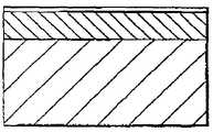
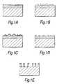
- FIG. 1 aillustrates the deposited layer of CsCl on the SiO 2 /Si
- FIG. 1 billustrates the formation of CsC1 islands on the substrate
- FIG. 1 cshows the formation of an Al film over the structure of FIG. 1 b;
- FIG. 1 dshows the structure of FIG. 1 c after ultrasonic agitation
- FIG. 1 eshows the effect of subjecting the structure of FIG. 1 d to RIE
- FIG. 2is a perspective view of a “tip-array” formed using CsC1 as resist
- FIG. 3is a graph of wall-angle and etch-rate
- FIG. 4is a perspective view of pillars formed by CsC1 hemispheres acting as resist;
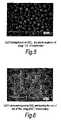
- FIG. 5is a plan view of an array of CsC1 hemispheres coated with Al;
- FIG. 6shows the array of FIG. 5 after removal of the hemispheres
- FIG. 7 ais a perspective view of wells formed in SiO 2 on Si;
- FIG. 7 bis a perspective view of a sectioned well in the structure of FIG. 7 a ;
- FIG. 8shows further examples of structures formed by using the methods of the invention.
- the tip fabrication illustrated in FIG. 2resulted from using the humidity value of the prevailing laboratory conditions (40%) and the CsCl thickness and development time were then chosen to give the desired distribution.
- the development timewas the time elapsed from removing the CsCl coated silicon from the deposition chamber to the RIE chamber at the moment of its pump down.
- the fabrication of tipswas carried out on n-type and p-type silicon substrates of ⁇ 100 ⁇ orientation as described above. Etching was carried out in equipment obtained from Oxford Plasma Technology (model RIE80, fitted with a 6.5′′ table).
- the conditions for island growthwere:—CsCl thickness 66 ⁇ ; relative humidity 40%; and 5 min. exposure time.
- FIG. 3shows the wall angle as a function of total pressure for a 1:10:20 mixture; average power 61 watts; 300 dc bias.
- the relation of wall angle to some of the other independent variablesis not shown, but the trends are as follows. There is an increasing etch rate with increasing dc bias; comparative insensitivity to Ar flow rate, at least for plus/minus a factor of two in flow-rate; and, wall angle and etch rate both increase with increasing CHF 3 flow rate.
- the procedure for well fabricationcf. FIG. 1 , is first to grow the CsCl island array on SiO 2 on Si: here we are interested in larger hemispheres, in the 0.5 to 1 micron range.
- a film of Alis then evaporated over this structure, and the Al film that coated the CsCl hemispheres is then caused to lift off, by means of ultrasonic agitation in water.
- the remaining Alcan then act as a resist, enabling holes to be etched in the SiO 2 .
- FIG. 5shows the CsCl islands coated by a 1050 ⁇ thick Al film. This array was made on a thermally grown oxide on silicon: the hydrophilic oxide was 3200 ⁇ thick. On to this CsCl/SiO 2 surface was evaporated pure Al to a thickness of 1060 ⁇ . The Al coated structure was ultrasonically agitated for 2 minutes.
- the composition of the layer forming the substrate for CsC1 growthcould also be WO 3 or Si 3 N 4 .
- the layer formation method for SiO 2is preferably thermal oxidation at a temperature of 1050–1350° C. for 1–8 hours, with an O 2 flow rate of 0.5–3 liters per minute.
- the layercan be formed by sputtering with a plasma gas comprising Ar and/or O 2 and/or N 2 , with RF power of 30–200 W for a period of 0.5–30 minutes, the target being either SiO 2 , Si or W.
- the chamber pressurecan be 1–50 m Torr.
- the formation of the CsC1 hemispherescan be done under a range of conditions, e.g.
- the resist layercan also be of various alternative materials to Al, e.g. Cr, Au, SiO 2 , Si 3 N 4 , and may be formed by vacuum evaporation or sputtering as appropriate.
- vacuum evaporationthis will normally be done at a chamber pressure of between 5 ⁇ 10 ⁇ 5 and 1 ⁇ 10 ⁇ 3 Pa, an evaporation rate of 0.2–50 angstrom/sec, and a substrate temperature of ⁇ 30 to +200° C.
- the plasma gas usedwould be Ar and/or O 2 and/or N 2 and the RF power 30–200 W for a period of 0.5–30 minutes.
- the targetcould be Al, Cr, Au, SiO 2 or Si, and the chamber pressure 1–50 m Torr.
- the ultrasonic agitation processcan also be carried out under a range of different conditions.
- the preferred frequency rangeis 24–100 kHz, power 13–130 W and power density 0.05–0.5 W/cm 2 .
- the time take for the ultrasonic agitation to be effectively completedmay be between 5 seconds and 60 minutes, and the preferred solvent is water.
- the evaporation of the resist materialis carried out at a grazing angle, this may vary between 15 and 90 degrees to the surface and the major/minor axis ratio of the ellipsoids thus formed will of course depend on this angle, but is generally up to 4-1.
- the rate between the resist (Al) thickness and the CsC1 mean diametermust be less than 0.2, and will generally be in the range of 0.005–0.2.
- Cesium chlorideis eroded by physical sputtering processes only, while the silicon is finally chemically removed.
- the selectivitywhich is the rate of silicon etching to that of the cesium chloride, can be determined from the physical characteristics of the tip structures.
- ⁇the sputtering rate
- the resistis being sputtered away the silicon is being etched vertically, at a rate v, so that a conical structure results in the Si.
- the present inventionenables the fabrication of pillars and cones of silicon in high packing density and of dimensions in the tens of nm region.
- the wells formed by the lift-off processcan be used to facilitate the formation of various other types of devices, particularly semiconductor devices.
- One specific application for which it has been found particularly usefulis in the fabrication of crystalline semiconductor heterostructures in which the lattice constants of the two component materials differ by less than 1 ⁇ 2%. Presently, these are usually formed by mismatched epitaxial methods.
- SLSstrained layer systems
- the epitaxial layers of the two componentsare thinner than the critical thickness for the formation of misfit dislocations with the result that the layers remain “pseudomorphic”, i.e. the atoms on either side of the interface remain in registry.
- the “in-plane” lattice constantsremain the same and the resulting strain can be deliberately used to modify the band structure of the system.
- the materialsare generally chosen (eg. GaAs and AlAs) so that the lattice mismatch is relatively small so that quite thick layers can be grown without dislocations forming.
- the effect of the dislocations formed near to interfaces or the resultant threading dislocations which can spread throughout the filmis to degrade the electrical and optical properties of the semiconductor.
- the electron mobility in InSb(the semiconductor having the highest mobility yet reported at room temperature of 78,000 cm 2/ Vs) can become as low as 100 cm 2 /Vs as measured by the Hall effect in a 10 nm InSb film grown on a GaAs substrate 10 (the lattice mismatch is 14% for this system).
- InSbis the favoured material for magnetoresistive or Hall sensors whose performance can consequently be severely reduced.
- the dislocationsalso act as electron-hole recombination centres and therefore limit minority carrier lifetimes, spoil transistor action and also act to prevent lasing and reduce LED and photodetector efficiencies. Dislocations can also act as shorting paths through p-n tunnel junctions, thereby degrading current voltage characteristics. The movement of dislocations induced by strong biassing electric fields can lead to the catastrophic failure of lasers and other devices.
- InSb/GaAsthere are many examples of semiconductor material systems where the formation of misfit dislocations at interfaces presents severe problems and prevents the full exploitation of otherwise admirable properties; particularly the Si/Si 1x Ge x system which offers the prospect of a new generation of Si based devices and the GaN related system, presently being developed for blue and uv solid-state light sources where no lattice matched substrates exist.
- Other examples of materials combinationsare InAs on GaAs where GaAs is chosen for substrates because of their cheapness and their electrically insulating properties; and the growth of compound semiconductors such GaAs on Si where the aim is to integrate optoelectronic, photonic or microelectronic devices on the same chip.
- film thicknesses exceeding ten micronsmay need to be grown. This is expensive and time consuming and may be undesirable for other reasons; e.g. leading to high device capacitances or preventing the use of the material sub-micron sensor applications.
- Two recent examples 11 of this for the InSb/GaAs systemare (i) the deposition of the first 10 monolayers at much reduced temperature (310° to 325° compared with 380°–400° C.) so that the extent of the island growth mode can be restricted to 22 nm (ii) the use of substrates of non-standard orientation where the growth mode and rate can be very different.
- Another variationhas been to grow the semiconductor on a substrate lithographically patterned with ridges or islands with the minimum feature size being of the order of one micron. If this characteristic length is smaller than the separation between threading dislocations, the local film quality then can approach that of the bulk material.
- the Si/Ge heterostructure combination 12As the first step an amorphous silicon dioxide film is deposited on a crystalline silicon substrate. Holes of diameter 100 nm are then opened up in the oxide and Ge is selectively grown on the Si within the exposed areas. The threading dislocations are bent and blocked by the oxide sidewalls and the interfacial misfit dislocations are buried within the holes. Chemical selectivity prevents the growth of the germanium directly an the oxides and a continuous film of Ge is eventually formed by sidewards epitaxial overgrowth of the material from the region of the holes. The depth, spacing of the holes and wall angle are all critical parameters.
- FIG. 8shows the three different structures which can be formed by varying the amounts of lateral overgrowth initiated from holes in thin silicon dioxide films.
- FIGS. 8( a ) and 8 ( b )are examples of “island” formations while FIG. 8( c ) shows a continuous film.
- a silicon dioxide layer 3is grown on a crystalline substrate 4 , and holes are created by the lithographic process described in references 18-22 .
- Thisconsists of (a) cesium chloride island deposition on the silicon dioxide coated substrate (b) aluminium film deposition on the surface (c) lift-off of the cesium chloride exposing the corresponding regions of the silicon dioxide (d) wet or dry etching of the silicon dioxide to create holes through to the crystalline substrate (e) removal of the aluminium film.
- the crystalline overgrowth ( 1 )is initiated at the bottom of these holes where a high density of dislocations ( 2 ) is formed.
- References 13-17are concerned with a method of reduction of dislocation densities during the growth of crystalline germanium on silicon or GaN on mismatched substrates. The method is directly applicable to other semiconductor heterostructures.
- the technique of growth through holes in a thin silicon dioxide filmcan in principle also be extended to improve the interface region between disparate crystalline materials systems such as metal/semiconductor, semiconductor/insulator or even metal—metal or metal-insulator combinations.
- the crystalline metalcould either be a conventional soft metal 23,24 , or the more brittle compounds such as MnAs 25,26 , MnSb 27 , NiMnSb 28,29,29 , PtMnSb 29 , CuMnSb 29 , LnPdSb 31 , CO 2 MnGe 32 or Cr02 33,34
- MnAs 25,26 , MnSb 27 , NiMnSb 28,29,29 , PtMnSb 29 , CuMnSb 29 , LnPdSb 31 , CO 2 MnGe 32 or Cr02 33,34The latter are of interest because of their magnetic properties and are more likely to be susceptible to mechanical problems at the interface such as microcracking and the formation of misfit dislocations.
- Crystalline semiconductor/insulator heterostructuresare mainly of interest because of the need to make highly perfect gate dielectrics or because of the drive to integrate optical waveguides and circuitry, or surface acoustic wave (SAW) delay lines with microelectronic devices. Often a high dielectric constant (relative permittivity) is desirable for these applications.
- the insulatorsare usually oxides; e.g. strontium titanate where good quality films have been grown on Si 35 , KtaO 3 , BaTiO 3 , TiO 2 , LiNbO 3 and lead lanthanum zirconate titanate (PLZT).
- Nanocrystalline magnetscan often be formed rather than smooth continuous film by varying the growth conditions to produce island growth or by subsequent annealing: e.g. MnA 9 36 , MnSb 37,38,39 and ErAs 40 .
Landscapes
- Engineering & Computer Science (AREA)
- Physics & Mathematics (AREA)
- Condensed Matter Physics & Semiconductors (AREA)
- General Physics & Mathematics (AREA)
- Manufacturing & Machinery (AREA)
- Computer Hardware Design (AREA)
- Microelectronics & Electronic Packaging (AREA)
- Power Engineering (AREA)
- Chemical & Material Sciences (AREA)
- Inorganic Chemistry (AREA)
- Crystals, And After-Treatments Of Crystals (AREA)
- Recrystallisation Techniques (AREA)
Abstract
Description
| chamber pressure: | 5 × 10⁻⁵ | to 1 × 10⁻³Pa, | ||
| evaporation rate | 0.2–50 | angstrom/sec | ||
| substrate temperature | −30 to +30 | |||
| thickness | ||||
| 1–200 | nm | |||
| ripening relative humidity | 0.63% | |||
| ripening time | 5 min–60 days | |||
angle between substrate surface and base of hemisphere wall: up to 90 degrees.
T=Ro/ω
While the resist is being sputtered away the silicon is being etched vertically, at a rate v, so that a conical structure results in the Si. The height, H, of the right regular cone will be,
H=Rov/ω
The cone (“tip”) angle φ is
φ=2 tan−1(ω/v)=2 tan−1(Ro/H)
For example, we have measured an average φ=28°, this gives a value of ω/v=4, which is the selectivity. For the case where sputtering of CsCl is only by vertical removal, at rate α, the rate term ω is replaced by α in the above equations.
T=Ro/(α2+η2)1/2
where η is the horizontal rate: and the tip angle is,
- 1. Mino Green and S. Tsuchiya, Submitted for Publication.
- 2. Mino Green and M. Garcia-Parajo, F. Khaleque and R. Murray. Appl. Phys. Lett., 63, 264 (1993).
- 3. H. W. Deckman and J. H. Dunsmuir, Appl. Phys. Lett., 41, 377 (1982).
- 4. H. Feng, R. Zella and P. J. Stiles, Appl. Phys. Lett 55, 1433 (1989).
- 5. C. Haginoya. M. Ishibashi and K. Koike, Appl. Phys. Lett., 71, 2934 (1997).
- 6. A. A. G: Driskill-Smith, D. G. Hasko and H. Ahmed, J. Vac. Sci. Technol B, 15, 2773 (1997).
- 7. A. A. G. Driskill-Smith, D. G. Hasko and H. Ahmed. Appl. Phys. Lett., 71, 3159 (1997).
- 8. Francois Foulon and Mino Green, Laser projection patterned etching of (100) GaAs by gaseous HCl and CH3C1, Appl. Phys A, 60, 377–381 (1995).
- 9. H. Dimigen and H. Luthe, Philips Tech. Rev., Rev., 35, 199 (1975).
- 10. Novel Semiconductor Material prepared by MBE & MOCVD R. A. Stradling Invited Talk at EPS Condensed Matter Conference (Lisbon) Physica Scripts T35 237–244 (1991).
- 11. Two dimensional growth of InSb thin films on GaAs (111) A substrates K. Kamisawa, H Yamaguchi & Y Hirayama App Phys Lett 76 589 (2000).
- 12. High quality Ge on Si by Epitaxial Necking T A Langdo, C W Leitz, M T Currie, E A. Fitzgerald, A Lochtefeld & D A Amoniadis Applied Physics Letters 76 3700 2000
- 13. Si/Si Ge dots grown by selective epitaxy L Vescan, C Dicker, A Hartman & A van der Hart Semiconductor Science & Technology 9 387 (1994)
- 14. Selective epitaxial growth of dot structures on patterned Si substrates by gas source molecular beam epitaxy E S Kim N Uami & Y Shiraki Semiconductor Science & Technology 14 257 (1999)
- 15. Lateral epitaxy of low defect density GaN layers via organometallic vapour phase epitaxy O Nam, M Bremser, T A Zhalova & R F Davis APL 71 2638 (1997)
- 16. Selective area and lateral epitaxial overgrowth of III-N materials by metal organic chemical vapour deposition J Park, P A Grudowski, C J Eitnig & R D Dupuis APL 73 333 (1998)
- 17. Pseudoepitaxy of gallium nitride thin films K Linthieium, T Gehrke, D Thomson, E Carlson, P Rajagopal, T Smith, D Batchelor & R Davis APL 75 196 (1999)
- 18. Mesoscopic Non-magnetic semiconductor magnetoresistive sensors fabricated with island lithography, M. Green, K Sassa, S A Solin, R A Stradling and S Tsuchiya, U.S. patent Pending
- 19. Shin Tsuchiya, Mino Green and R R A Syms, “Structural Fabrication Using Cesium Chloride Island Arrays as Resist in a Fluorocarbon Reactive Ion Etching Plasma”, Electrochemical and Solid-
State Letters 3, 44–64 (2000) - 20. M. Green, M Garcia-Parajo, F Khaleque and R Murray, “Quantum pillar structures on n+gallium arsenide fabricated using natural lithography”, Appl. Phys. Lett, 66, 264 (1993)
- 21. Mino Green and Shin Tsuchiya, “Mesoscopic hemisphere arrays for use as resist in solid state structure” J. Vac. Sci. & Tech. B. 17, 2074–2083 (1999)
- 22. F. Khaleque, “E-beam lithography and dry processing for sub-micron fabrication” PhD Thesis (Electrical Engineering Department Imperial College) University of London, 1990. M. F. Garcia-Parajo, “Natural lithography based on alkali-halide thin films for semiconductor sub-micron fabrication” PhD Thesis (Electrical Engineering Department, Imperial College) University of London 1993.
- 23. Single crystal Fe films groown on InAs (001) by molecular beam epitaxy Y B Xu, E T M Kernohan, M Teslepi, J A C Bland & S Holmes APL 73 399 (1998).
- 24. Ferromagnetic metal/semiconductor hybrid structures for magnetoelectronics Y B Xu, D J Freeland, E T Kernohan, W Y Lee, M Teslepi, C M Guertier, C A F Vaz, J A C Bland, S Holmes, N K Patel & D A Ritchie J App. Phys 85 5369 (1999).
- 25. Making Nonmagnetic Semiconductors Ferromagnetic H Ohno Science 281 951 (1998).
- 26 Growth control of MnAs on GaAs (001) by reflection high-energy electron diffraction F Schippan, M Kastner, L Daweritz & K H Ploog APL 76 834 (2000)
- 27. Influence of GaAs (001) surface termination on the n-plane magnetic anisotropies of MnSb epitaxial films H Akinaga, S Miyanishi, W van dRoy, J de Boeck & G Borghs APL 73 3285 (1998).
- 28. Deposition of high-quality NiMnSb magnetic films at moderate temperatures J A Caballero, Y D Perk, A Cabbibo, J R Childress, F Petroff & R Morei, J App Phys 81 2740 (1997).
- 29. Optical spectroscopy of half metallic ferromagnetic Heusler alloy thin films. PtMnSb, NiMnSb & CuMnSb J F Bobo, P R Johnson, M Kautzky, F B Mancoff, E Tuncci, R. L. White & B M Clemens J App Phys 81 4164 (1997).
- 30. Dielectric tensor for magneto-optic NiMnSb X Gao, J A Woollam, R D Kirby, D J Sellmyer, C T Tanaka, J Nowak & J S Moodera Phys Rev 59B 9965 (1999).
- 31. Antimonides with the half-Heusler structure; new thermoelectric materials K Mastonardi, D Yound, C C Wang, P Khalifah, R J Cava & A P Ramirez APL 74 1415 (1999).
- 32. Epitaxial growth and magnetic properties of single crystal C02MnGe Heusler alloy films on GaAs (001) T Ambrose, J J Krebs & G A Prinz APL 76 3280 (2000)
- 33. Highly spin-polarised chromium dioxide thin films produced by chemical vapour deposition from chromyl chloride W J DeSisto, P R Broussard, T F Ambrose, B E Nadgorny & M S Osofaky APL 76 3789 (2000).
- 34. Production and magnetotransport properties of CrO2films L Ranno, A Barry & J M D Coey J Apps Phys 81 5774 (1997).
- 35. Field effect transistors with SrTiO3gate dielectric on Si K Eisenbeiser, J M Finder, Z, Yu, J Randani. J A Curless J A Hallmark, R Droopsd, W J Ooms, L Salem, S Bradshaw & C D Overgaard APL 76 1324 (2000).
- 36. Giant magnetoresistance in a low temperature GaAs/MnAs nanoscale ferromagnet hybrid structure P J Wellman, J M Garcia, J L Feng & P M Petroff APL 73 3291 (1998).
- 37. Room tempeerature thousand fold magnetoresistive change in MnSb granular films H Akinaga, M Mizuguchi, K Ono & M Oshima APL 76 357 (2000).
- 38. Crystallographic and magneto-optical studies of nanoscaled MnSb dots grown on GaAs M Mizuguchi, H Akinaga, K Ono & M Oshima APL 76 1743 (2000).
- 39. Room temperature photoinduced magnetoresistive effect in GaAs including MnSb nanomagnets H Akinaga. M Mizuguchi, K Ono and M Oshima APL 76 2600 (2000).
- 40. Fluctuation controlled hopping of bound magnetic polarons in Er:GaAs nanocomposites D R Schmidt, A G Petujkhov, M Foygel, J P Ibbotson & S J Allen Phys Rev Lett 82 823 (1999).
- 41. Controlling magnetic ordering in coupled nanomagnetic arrays R P Cowburn, A O Adeyeye & M E Welland New Journal of
Physics 1 116.1–16.0 (1999). - 42. Magnetisation reversal in long chains of submicronic Co dots J I Martin et al Applied Phys. Lett 72 255 (1998).
- 43. Thin Horizontal Plane Hall Sensors for ReadHeads in Magnetic Recording. S A Solin, R Stradling, T Thin and A J Bennett Meas Sci & Techn 8 1174 1181 (1997)
- 44. Narrow gap semiconductor Hall Sensors for ReadHeads in Magnetic Recording S A Solin, R A Stradling, J W Bennett & T Proc. Int Conf on Narrow Gap Semiconductors (Shanghai) World Scientific 1997 P249.
- 45. Thin Horizontal-Plane Hall Sensors for Read Heads in Magnetic Recording, J Bennett, S Solin, T Thio and R Stradling, U.S. patent application Ser. No. 08/781,994.
Claims (14)
Priority Applications (1)
| Application Number | Priority Date | Filing Date | Title |
|---|---|---|---|
| US11/352,517US7419908B2 (en) | 1999-08-17 | 2006-02-10 | Process for making an array of wells |
Applications Claiming Priority (2)
| Application Number | Priority Date | Filing Date | Title |
|---|---|---|---|
| GBGB9919479.7AGB9919479D0 (en) | 1999-08-17 | 1999-08-17 | Island arrays |
| PCT/GB2000/003202WO2001013414A1 (en) | 1999-08-17 | 2000-08-17 | A process for making island arrays |
Related Child Applications (1)
| Application Number | Title | Priority Date | Filing Date |
|---|---|---|---|
| US11/352,517ContinuationUS7419908B2 (en) | 1999-08-17 | 2006-02-10 | Process for making an array of wells |
Publications (1)
| Publication Number | Publication Date |
|---|---|
| US7033936B1true US7033936B1 (en) | 2006-04-25 |
Family
ID=10859335
Family Applications (2)
| Application Number | Title | Priority Date | Filing Date |
|---|---|---|---|
| US10/049,736Expired - Fee RelatedUS7033936B1 (en) | 1999-08-17 | 2000-08-17 | Process for making island arrays |
| US11/352,517Expired - Fee RelatedUS7419908B2 (en) | 1999-08-17 | 2006-02-10 | Process for making an array of wells |
Family Applications After (1)
| Application Number | Title | Priority Date | Filing Date |
|---|---|---|---|
| US11/352,517Expired - Fee RelatedUS7419908B2 (en) | 1999-08-17 | 2006-02-10 | Process for making an array of wells |
Country Status (3)
| Country | Link |
|---|---|
| US (2) | US7033936B1 (en) |
| GB (1) | GB9919479D0 (en) |
| WO (1) | WO2001013414A1 (en) |
Cited By (59)
| Publication number | Priority date | Publication date | Assignee | Title |
|---|---|---|---|---|
| US20050054180A1 (en)* | 2003-09-09 | 2005-03-10 | Sang Han | Threading-dislocation-free nanoheteroepitaxy of Ge on Si using self-directed touch-down of Ge through a thin SiO2 layer |
| US20050142385A1 (en)* | 2002-09-30 | 2005-06-30 | Sungho Jin | Ultra-high-density information storage media and methods for making the same |
| US20060073681A1 (en)* | 2004-09-08 | 2006-04-06 | Han Sang M | Nanoheteroepitaxy of Ge on Si as a foundation for group III-V and II-VI integration |
| US20060110568A1 (en)* | 2004-11-23 | 2006-05-25 | Imation Corp. | Multi-layers optical data storage disk masters |
| US20060131261A1 (en)* | 1999-08-17 | 2006-06-22 | Imperial Innovations Limited | Process for making island arrays |
| US20060292719A1 (en)* | 2005-05-17 | 2006-12-28 | Amberwave Systems Corporation | Lattice-mismatched semiconductor structures with reduced dislocation defect densities and related methods for device fabrication |
| US20070054465A1 (en)* | 2005-09-07 | 2007-03-08 | Amberwave Systems Corporation | Lattice-mismatched semiconductor structures on insulators |
| US20070054467A1 (en)* | 2005-09-07 | 2007-03-08 | Amberwave Systems Corporation | Methods for integrating lattice-mismatched semiconductor structure on insulators |
| US20070181977A1 (en)* | 2005-07-26 | 2007-08-09 | Amberwave Systems Corporation | Solutions for integrated circuit integration of alternative active area materials |
| US20070267722A1 (en)* | 2006-05-17 | 2007-11-22 | Amberwave Systems Corporation | Lattice-mismatched semiconductor structures with reduced dislocation defect densities and related methods for device fabrication |
| US20080001169A1 (en)* | 2006-03-24 | 2008-01-03 | Amberwave Systems Corporation | Lattice-mismatched semiconductor structures and related methods for device fabrication |
| US20080070355A1 (en)* | 2006-09-18 | 2008-03-20 | Amberwave Systems Corporation | Aspect ratio trapping for mixed signal applications |
| US20080073667A1 (en)* | 2006-09-27 | 2008-03-27 | Amberwave Systems Corporation | Tri-gate field-effect transistors formed by aspect ratio trapping |
| US20080187018A1 (en)* | 2006-10-19 | 2008-08-07 | Amberwave Systems Corporation | Distributed feedback lasers formed via aspect ratio trapping |
| US20090001936A1 (en)* | 2002-11-05 | 2009-01-01 | Mino Green | Structured silicon anode |
| US20090039361A1 (en)* | 2005-05-17 | 2009-02-12 | Amberwave Systems Corporation | Lattice-mismatched semiconductor structures with reduced dislocation defect densities and related methods for device fabrication |
| US20090042344A1 (en)* | 2007-06-15 | 2009-02-12 | Amberwave Systems Corporation | InP-Based Transistor Fabrication |
| US20090079322A1 (en)* | 2007-09-21 | 2009-03-26 | Kabushiki Kaisha Toshiba | Light-transmitting metal electrode having hyperfine structure and process for preparation thereof |
| US20100151324A1 (en)* | 2006-01-23 | 2010-06-17 | Mino Green | Method of fabricating fibres composed of silicon or a silicon-based material and their use in lithium rechargeable batteries |
| US20100178565A1 (en)* | 2007-07-17 | 2010-07-15 | Mino Green | Method of fabricating structured particles composed of silicon or a silicon-based material and their use in lithium rechargeable batteries |
| US20100190057A1 (en)* | 2007-07-17 | 2010-07-29 | Mino Green | Method |
| US20100196760A1 (en)* | 2007-07-17 | 2010-08-05 | Mino Green | Production |
| US20100218815A1 (en)* | 2009-11-18 | 2010-09-02 | International Business Machines Corporation | Holey electrode grids for photovoltaic cells with subwavelength and superwavelength feature sizes |
| US20100233539A1 (en)* | 2006-01-23 | 2010-09-16 | Mino Green | Method of etching a silicon-based material |
| US7875958B2 (en) | 2006-09-27 | 2011-01-25 | Taiwan Semiconductor Manufacturing Company, Ltd. | Quantum tunneling devices and circuits with lattice-mismatched semiconductor structures |
| US20110049568A1 (en)* | 2005-05-17 | 2011-03-03 | Taiwan Semiconductor Manufacturing Company, Ltd. | Lattice-Mismatched Semiconductor Structures with Reduced Dislocation Defect Densities and Related Methods for Device Fabrication |
| US20110186858A1 (en)* | 2009-08-04 | 2011-08-04 | John Roberts | Gallium Nitride Power Devices Using Island Topography |
| WO2011124893A2 (en) | 2010-04-09 | 2011-10-13 | Nexeon Limited | A method of fabricating structured particles composed of silicon or a silicon-based material and their use in lithium rechargeable batteries |
| US8173551B2 (en) | 2006-09-07 | 2012-05-08 | Taiwan Semiconductor Manufacturing Co., Ltd. | Defect reduction using aspect ratio trapping |
| US8237151B2 (en) | 2009-01-09 | 2012-08-07 | Taiwan Semiconductor Manufacturing Company, Ltd. | Diode-based devices and methods for making the same |
| US8253211B2 (en) | 2008-09-24 | 2012-08-28 | Taiwan Semiconductor Manufacturing Company, Ltd. | Semiconductor sensor structures with reduced dislocation defect densities |
| US20120225517A1 (en)* | 2009-11-17 | 2012-09-06 | Jun-Ying Zhang | Texturing surface of light-absorbing substrate |
| US8274097B2 (en) | 2008-07-01 | 2012-09-25 | Taiwan Semiconductor Manufacturing Company, Ltd. | Reduction of edge effects from aspect ratio trapping |
| US8304805B2 (en) | 2009-01-09 | 2012-11-06 | Taiwan Semiconductor Manufacturing Company, Ltd. | Semiconductor diodes fabricated by aspect ratio trapping with coalesced films |
| US8344242B2 (en) | 2007-09-07 | 2013-01-01 | Taiwan Semiconductor Manufacturing Company, Ltd. | Multi-junction solar cells |
| US8384196B2 (en) | 2008-09-19 | 2013-02-26 | Taiwan Semiconductor Manufacturing Company, Ltd. | Formation of devices by epitaxial layer overgrowth |
| CN103030096A (en)* | 2011-10-09 | 2013-04-10 | 中国科学院高能物理研究所 | Silicon material with nano-structure surface and manufacturing method thereof |
| US8624103B2 (en) | 2007-04-09 | 2014-01-07 | Taiwan Semiconductor Manufacturing Company, Ltd. | Nitride-based multi-junction solar cell modules and methods for making the same |
| US8629446B2 (en) | 2009-04-02 | 2014-01-14 | Taiwan Semiconductor Manufacturing Company, Ltd. | Devices formed from a non-polar plane of a crystalline material and method of making the same |
| US20140151326A1 (en)* | 2008-02-25 | 2014-06-05 | Kabushiki Kaisha Toshiba | Light-transmitting metal electrode and process for production thereof |
| US20140166092A1 (en)* | 2012-12-14 | 2014-06-19 | Robert Bosch Gmbh | Method of Fabricating Nanocone Texture on Glass and Transparent Conductors |
| US8791508B2 (en) | 2010-04-13 | 2014-07-29 | Gan Systems Inc. | High density gallium nitride devices using island topology |
| US8822248B2 (en) | 2008-06-03 | 2014-09-02 | Taiwan Semiconductor Manufacturing Company, Ltd. | Epitaxial growth of crystalline material |
| US8932759B2 (en) | 2008-10-10 | 2015-01-13 | Nexeon Ltd. | Method of fabricating structured particles composed of silicon or a silicon-based material |
| US8945774B2 (en) | 2010-06-07 | 2015-02-03 | Nexeon Ltd. | Additive for lithium ion rechageable battery cells |
| US8962183B2 (en) | 2009-05-07 | 2015-02-24 | Nexeon Limited | Method of making silicon anode material for rechargeable cells |
| US8981427B2 (en) | 2008-07-15 | 2015-03-17 | Taiwan Semiconductor Manufacturing Company, Ltd. | Polishing of small composite semiconductor materials |
| US9064947B2 (en) | 2009-08-04 | 2015-06-23 | Gan Systems Inc. | Island matrixed gallium nitride microwave and power switching transistors |
| US9153509B2 (en) | 2009-08-04 | 2015-10-06 | Gan Systems Inc. | Fault tolerant design for large area nitride semiconductor devices |
| US9184438B2 (en) | 2008-10-10 | 2015-11-10 | Nexeon Ltd. | Method of fabricating structured particles composed of silicon or a silicon-based material and their use in lithium rechargeable batteries |
| US9252426B2 (en) | 2007-05-11 | 2016-02-02 | Nexeon Limited | Silicon anode for a rechargeable battery |
| CN105428221A (en)* | 2015-12-23 | 2016-03-23 | 中国科学院高能物理研究所 | Method for improving photoresist dropping |
| US9508890B2 (en) | 2007-04-09 | 2016-11-29 | Taiwan Semiconductor Manufacturing Company, Ltd. | Photovoltaics on silicon |
| US9608272B2 (en) | 2009-05-11 | 2017-03-28 | Nexeon Limited | Composition for a secondary battery cell |
| US9647263B2 (en) | 2010-09-03 | 2017-05-09 | Nexeon Limited | Electroactive material |
| US9853292B2 (en) | 2009-05-11 | 2017-12-26 | Nexeon Limited | Electrode composition for a secondary battery cell |
| US9871248B2 (en) | 2010-09-03 | 2018-01-16 | Nexeon Limited | Porous electroactive material |
| US9984872B2 (en) | 2008-09-19 | 2018-05-29 | Taiwan Semiconductor Manufacturing Company, Ltd. | Fabrication and structures of crystalline material |
| US20180288026A1 (en)* | 2017-04-03 | 2018-10-04 | Microsoft Technology Licensing, Llc | Password state machine for accessing protected resources |
Families Citing this family (10)
| Publication number | Priority date | Publication date | Assignee | Title |
|---|---|---|---|---|
| US6353317B1 (en) | 2000-01-19 | 2002-03-05 | Imperial College Of Science, Technology And Medicine | Mesoscopic non-magnetic semiconductor magnetoresistive sensors fabricated with island lithography |
| GB2377026A (en)* | 2001-06-29 | 2002-12-31 | Imp College Innovations Ltd | Electrically addressable electrochemical cell array |
| GB0413243D0 (en)* | 2004-06-14 | 2004-07-14 | Imp College Innovations Ltd | Transmissive element |
| US7934921B2 (en)* | 2007-10-31 | 2011-05-03 | Hitachi Global Storage Technologies Netherlands B.V. | Apparatus, system, and method for guided growth of patterned media using monodisperse nanospheres |
| US9005548B2 (en)* | 2009-02-25 | 2015-04-14 | California Institute Of Technology | Methods for fabricating high aspect ratio probes and deforming high aspect ratio nanopillars and micropillars |
| KR20120092091A (en)* | 2009-06-26 | 2012-08-20 | 캘리포니아 인스티튜트 오브 테크놀로지 | Methods for fabricating passivated silicon nanowires and devices thus obtained |
| EP2502264A4 (en) | 2009-11-19 | 2015-09-16 | California Inst Of Techn | METHODS OF MANUFACTURING SELF-ALIGNMENT DEVICES ON SEMICONDUCTORS |
| US9018684B2 (en) | 2009-11-23 | 2015-04-28 | California Institute Of Technology | Chemical sensing and/or measuring devices and methods |
| GB201122315D0 (en)* | 2011-12-23 | 2012-02-01 | Nexeon Ltd | Etched silicon structures, method of forming etched silicon structures and uses thereof |
| CN109742124B (en)* | 2019-01-11 | 2021-01-22 | 京东方科技集团股份有限公司 | Preparation method of OLED display device, OLED display device and display device |
Citations (1)
| Publication number | Priority date | Publication date | Assignee | Title |
|---|---|---|---|---|
| US6153010A (en)* | 1997-04-11 | 2000-11-28 | Nichia Chemical Industries Ltd. | Method of growing nitride semiconductors, nitride semiconductor substrate and nitride semiconductor device |
Family Cites Families (5)
| Publication number | Priority date | Publication date | Assignee | Title |
|---|---|---|---|---|
| EP0191503A3 (en)* | 1980-04-10 | 1986-09-10 | Massachusetts Institute Of Technology | Method of producing sheets of crystalline material |
| US5676853A (en)* | 1996-05-21 | 1997-10-14 | Micron Display Technology, Inc. | Mask for forming features on a semiconductor substrate and a method for forming the mask |
| US6195228B1 (en)* | 1997-01-06 | 2001-02-27 | Nec Research Institute, Inc. | Thin, horizontal-plane hall sensors for read-heads in magnetic recording |
| GB9919479D0 (en)* | 1999-08-17 | 1999-10-20 | Imperial College | Island arrays |
| US6353317B1 (en)* | 2000-01-19 | 2002-03-05 | Imperial College Of Science, Technology And Medicine | Mesoscopic non-magnetic semiconductor magnetoresistive sensors fabricated with island lithography |
- 1999
- 1999-08-17GBGBGB9919479.7Apatent/GB9919479D0/ennot_activeCeased
- 2000
- 2000-08-17USUS10/049,736patent/US7033936B1/ennot_activeExpired - Fee Related
- 2000-08-17WOPCT/GB2000/003202patent/WO2001013414A1/enactiveApplication Filing
- 2006
- 2006-02-10USUS11/352,517patent/US7419908B2/ennot_activeExpired - Fee Related
Patent Citations (1)
| Publication number | Priority date | Publication date | Assignee | Title |
|---|---|---|---|---|
| US6153010A (en)* | 1997-04-11 | 2000-11-28 | Nichia Chemical Industries Ltd. | Method of growing nitride semiconductors, nitride semiconductor substrate and nitride semiconductor device |
Non-Patent Citations (2)
| Title |
|---|
| Green et al., "Quantum pillar structures on n+ gallium arsenide fabricated using 'natural' lithography", 1993, pp. 264-266.* |
| Haginoya et al., "Nanostructure array fabrication with a size-controllable natural lithography", 1997, p. 2934-2936.* |
Cited By (144)
| Publication number | Priority date | Publication date | Assignee | Title |
|---|---|---|---|---|
| US20060131261A1 (en)* | 1999-08-17 | 2006-06-22 | Imperial Innovations Limited | Process for making island arrays |
| US7419908B2 (en)* | 1999-08-17 | 2008-09-02 | Imperial Innovations Limited | Process for making an array of wells |
| US20050142385A1 (en)* | 2002-09-30 | 2005-06-30 | Sungho Jin | Ultra-high-density information storage media and methods for making the same |
| US8384058B2 (en) | 2002-11-05 | 2013-02-26 | Nexeon Ltd. | Structured silicon anode |
| US20110107590A1 (en)* | 2002-11-05 | 2011-05-12 | Nexeon Limited | Structured silicon anode |
| US7842535B2 (en) | 2002-11-05 | 2010-11-30 | Nexeon Ltd. | Structured silicon anode |
| US8017430B2 (en) | 2002-11-05 | 2011-09-13 | Nexeon Ltd. | Structured silicon anode |
| US20090001936A1 (en)* | 2002-11-05 | 2009-01-01 | Mino Green | Structured silicon anode |
| US7888244B2 (en) | 2003-09-09 | 2011-02-15 | Stc.Unm | Threading-dislocation-free nanoheteroepitaxy of Ge on Si using self-directed touch-down of Ge through a thin SiO2 layer |
| US20050054180A1 (en)* | 2003-09-09 | 2005-03-10 | Sang Han | Threading-dislocation-free nanoheteroepitaxy of Ge on Si using self-directed touch-down of Ge through a thin SiO2 layer |
| US7579263B2 (en)* | 2003-09-09 | 2009-08-25 | Stc.Unm | Threading-dislocation-free nanoheteroepitaxy of Ge on Si using self-directed touch-down of Ge through a thin SiO2 layer |
| US20060073681A1 (en)* | 2004-09-08 | 2006-04-06 | Han Sang M | Nanoheteroepitaxy of Ge on Si as a foundation for group III-V and II-VI integration |
| US20060110568A1 (en)* | 2004-11-23 | 2006-05-25 | Imation Corp. | Multi-layers optical data storage disk masters |
| US9431243B2 (en) | 2005-05-17 | 2016-08-30 | Taiwan Semiconductor Manufacturing Company, Ltd. | Lattice-mismatched semiconductor structures with reduced dislocation defect densities and related methods for device fabrication |
| US8629477B2 (en) | 2005-05-17 | 2014-01-14 | Taiwan Semiconductor Manufacturing Company, Ltd. | Lattice-mismatched semiconductor structures with reduced dislocation defect densities and related methods for device fabrication |
| US9153645B2 (en) | 2005-05-17 | 2015-10-06 | Taiwan Semiconductor Manufacturing Company, Ltd. | Lattice-mismatched semiconductor structures with reduced dislocation defect densities and related methods for device fabrication |
| US20090039361A1 (en)* | 2005-05-17 | 2009-02-12 | Amberwave Systems Corporation | Lattice-mismatched semiconductor structures with reduced dislocation defect densities and related methods for device fabrication |
| US9219112B2 (en) | 2005-05-17 | 2015-12-22 | Taiwan Semiconductor Manufacturing Company, Ltd. | Lattice-mismatched semiconductor structures with reduced dislocation defect densities and related methods for device fabrication |
| US10522629B2 (en) | 2005-05-17 | 2019-12-31 | Taiwan Semiconductor Manufacturing Company, Ltd. | Lattice-mismatched semiconductor structures with reduced dislocation defect densities and related methods for device fabrication |
| US8519436B2 (en) | 2005-05-17 | 2013-08-27 | Taiwan Semiconductor Manufacturing Company, Ltd. | Lattice-mismatched semiconductor structures with reduced dislocation defect densities and related methods for device fabrication |
| US11251272B2 (en) | 2005-05-17 | 2022-02-15 | Taiwan Semiconductor Manufacturing Company, Ltd. | Lattice-mismatched semiconductor structures with reduced dislocation defect densities and related methods for device fabrication |
| US8796734B2 (en) | 2005-05-17 | 2014-08-05 | Taiwan Semiconductor Manufacturing Company, Ltd. | Lattice-mismatched semiconductor structures with reduced dislocation defect densities and related methods for device fabrication |
| US8324660B2 (en) | 2005-05-17 | 2012-12-04 | Taiwan Semiconductor Manufacturing Company, Ltd. | Lattice-mismatched semiconductor structures with reduced dislocation defect densities and related methods for device fabrication |
| US8987028B2 (en) | 2005-05-17 | 2015-03-24 | Taiwan Semiconductor Manufacturing Company, Ltd. | Lattice-mismatched semiconductor structures with reduced dislocation defect densities and related methods for device fabrication |
| US20110049568A1 (en)* | 2005-05-17 | 2011-03-03 | Taiwan Semiconductor Manufacturing Company, Ltd. | Lattice-Mismatched Semiconductor Structures with Reduced Dislocation Defect Densities and Related Methods for Device Fabrication |
| US20060292719A1 (en)* | 2005-05-17 | 2006-12-28 | Amberwave Systems Corporation | Lattice-mismatched semiconductor structures with reduced dislocation defect densities and related methods for device fabrication |
| US20070181977A1 (en)* | 2005-07-26 | 2007-08-09 | Amberwave Systems Corporation | Solutions for integrated circuit integration of alternative active area materials |
| US7626246B2 (en) | 2005-07-26 | 2009-12-01 | Amberwave Systems Corporation | Solutions for integrated circuit integration of alternative active area materials |
| US20070054467A1 (en)* | 2005-09-07 | 2007-03-08 | Amberwave Systems Corporation | Methods for integrating lattice-mismatched semiconductor structure on insulators |
| US7638842B2 (en) | 2005-09-07 | 2009-12-29 | Amberwave Systems Corporation | Lattice-mismatched semiconductor structures on insulators |
| US20070054465A1 (en)* | 2005-09-07 | 2007-03-08 | Amberwave Systems Corporation | Lattice-mismatched semiconductor structures on insulators |
| US20100151324A1 (en)* | 2006-01-23 | 2010-06-17 | Mino Green | Method of fabricating fibres composed of silicon or a silicon-based material and their use in lithium rechargeable batteries |
| US8597831B2 (en) | 2006-01-23 | 2013-12-03 | Nexeon Ltd. | Method of fabricating fibres composed of silicon or a silicon-based material and their use in lithium rechargeable batteries |
| US20100233539A1 (en)* | 2006-01-23 | 2010-09-16 | Mino Green | Method of etching a silicon-based material |
| US9583762B2 (en) | 2006-01-23 | 2017-02-28 | Nexeon Limited | Method of fabricating fibres composed of silicon or a silicon-based material and their use in lithium rechargeable batteries |
| US8101298B2 (en) | 2006-01-23 | 2012-01-24 | Nexeon Ltd. | Method of fabricating fibres composed of silicon or a silicon-based material and their use in lithium rechargeable batteries |
| US8585918B2 (en) | 2006-01-23 | 2013-11-19 | Nexeon Ltd. | Method of etching a silicon-based material |
| US7777250B2 (en) | 2006-03-24 | 2010-08-17 | Taiwan Semiconductor Manufacturing Company, Ltd. | Lattice-mismatched semiconductor structures and related methods for device fabrication |
| US8878243B2 (en) | 2006-03-24 | 2014-11-04 | Taiwan Semiconductor Manufacturing Company, Ltd. | Lattice-mismatched semiconductor structures and related methods for device fabrication |
| US20080001169A1 (en)* | 2006-03-24 | 2008-01-03 | Amberwave Systems Corporation | Lattice-mismatched semiconductor structures and related methods for device fabrication |
| US10074536B2 (en) | 2006-03-24 | 2018-09-11 | Taiwan Semiconductor Manufacturing Company, Ltd. | Lattice-mismatched semiconductor structures and related methods for device fabrication |
| US20070267722A1 (en)* | 2006-05-17 | 2007-11-22 | Amberwave Systems Corporation | Lattice-mismatched semiconductor structures with reduced dislocation defect densities and related methods for device fabrication |
| US8847279B2 (en) | 2006-09-07 | 2014-09-30 | Taiwan Semiconductor Manufacturing Company, Ltd. | Defect reduction using aspect ratio trapping |
| US8173551B2 (en) | 2006-09-07 | 2012-05-08 | Taiwan Semiconductor Manufacturing Co., Ltd. | Defect reduction using aspect ratio trapping |
| US9318325B2 (en) | 2006-09-07 | 2016-04-19 | Taiwan Semiconductor Manufacturing Company, Ltd. | Defect reduction using aspect ratio trapping |
| US9818819B2 (en) | 2006-09-07 | 2017-11-14 | Taiwan Semiconductor Manufacturing Company, Ltd. | Defect reduction using aspect ratio trapping |
| US20080070355A1 (en)* | 2006-09-18 | 2008-03-20 | Amberwave Systems Corporation | Aspect ratio trapping for mixed signal applications |
| US8216951B2 (en) | 2006-09-27 | 2012-07-10 | Taiwan Semiconductor Manufacturing Company, Ltd. | Quantum tunneling devices and circuits with lattice-mismatched semiconductor structures |
| US7799592B2 (en) | 2006-09-27 | 2010-09-21 | Taiwan Semiconductor Manufacturing Company, Ltd. | Tri-gate field-effect transistors formed by aspect ratio trapping |
| US9105522B2 (en) | 2006-09-27 | 2015-08-11 | Taiwan Semiconductor Manufacturing Company, Ltd. | Quantum tunneling devices and circuits with lattice-mismatched semiconductor structures |
| US20080073667A1 (en)* | 2006-09-27 | 2008-03-27 | Amberwave Systems Corporation | Tri-gate field-effect transistors formed by aspect ratio trapping |
| US7875958B2 (en) | 2006-09-27 | 2011-01-25 | Taiwan Semiconductor Manufacturing Company, Ltd. | Quantum tunneling devices and circuits with lattice-mismatched semiconductor structures |
| US8860160B2 (en) | 2006-09-27 | 2014-10-14 | Taiwan Semiconductor Manufacturing Company, Ltd. | Quantum tunneling devices and circuits with lattice-mismatched semiconductor structures |
| US9559712B2 (en) | 2006-09-27 | 2017-01-31 | Taiwan Semiconductor Manufacturing Company, Ltd. | Quantum tunneling devices and circuits with lattice-mismatched semiconductor structures |
| US8629047B2 (en) | 2006-09-27 | 2014-01-14 | Taiwan Semiconductor Manufacturing Company, Ltd. | Quantum tunneling devices and circuits with lattice-mismatched semiconductor structures |
| US10468551B2 (en) | 2006-10-19 | 2019-11-05 | Taiwan Semiconductor Manufacturing Company, Ltd. | Light-emitter-based devices with lattice-mismatched semiconductor structures |
| US20080187018A1 (en)* | 2006-10-19 | 2008-08-07 | Amberwave Systems Corporation | Distributed feedback lasers formed via aspect ratio trapping |
| US8502263B2 (en) | 2006-10-19 | 2013-08-06 | Taiwan Semiconductor Manufacturing Company, Ltd. | Light-emitter-based devices with lattice-mismatched semiconductor structures |
| US9543472B2 (en) | 2007-04-09 | 2017-01-10 | Taiwan Semiconductor Manufacturing Company, Ltd. | Diode-based devices and methods for making the same |
| US9508890B2 (en) | 2007-04-09 | 2016-11-29 | Taiwan Semiconductor Manufacturing Company, Ltd. | Photovoltaics on silicon |
| US9040331B2 (en) | 2007-04-09 | 2015-05-26 | Taiwan Semiconductor Manufacturing Company, Ltd. | Diode-based devices and methods for making the same |
| US9853118B2 (en) | 2007-04-09 | 2017-12-26 | Taiwan Semiconductor Manufacturing Company, Ltd. | Diode-based devices and methods for making the same |
| US8624103B2 (en) | 2007-04-09 | 2014-01-07 | Taiwan Semiconductor Manufacturing Company, Ltd. | Nitride-based multi-junction solar cell modules and methods for making the same |
| US10680126B2 (en) | 2007-04-09 | 2020-06-09 | Taiwan Semiconductor Manufacturing Company, Ltd. | Photovoltaics on silicon |
| US9231073B2 (en) | 2007-04-09 | 2016-01-05 | Taiwan Semiconductor Manufacturing Company, Ltd. | Diode-based devices and methods for making the same |
| US9853176B2 (en) | 2007-04-09 | 2017-12-26 | Taiwan Semiconductor Manufacturing Company, Ltd. | Nitride-based multi-junction solar cell modules and methods for making the same |
| US9449868B2 (en) | 2007-04-09 | 2016-09-20 | Taiwan Semiconductor Manufacutring Company, Ltd. | Methods of forming semiconductor diodes by aspect ratio trapping with coalesced films |
| US9871249B2 (en) | 2007-05-11 | 2018-01-16 | Nexeon Limited | Silicon anode for a rechargeable battery |
| US9252426B2 (en) | 2007-05-11 | 2016-02-02 | Nexeon Limited | Silicon anode for a rechargeable battery |
| US9780190B2 (en) | 2007-06-15 | 2017-10-03 | Taiwan Semiconductor Manufacturing Company, Ltd. | InP-based transistor fabrication |
| US8329541B2 (en) | 2007-06-15 | 2012-12-11 | Taiwan Semiconductor Manufacturing Company, Ltd. | InP-based transistor fabrication |
| US20090042344A1 (en)* | 2007-06-15 | 2009-02-12 | Amberwave Systems Corporation | InP-Based Transistor Fabrication |
| US8870975B2 (en) | 2007-07-17 | 2014-10-28 | Nexeon Ltd. | Method of fabricating structured particles composed of silicon or a silicon-based material and their use in lithium rechargeable batteries |
| US9871244B2 (en) | 2007-07-17 | 2018-01-16 | Nexeon Limited | Method of fabricating structured particles composed of silicon or a silicon-based material and their use in lithium rechargeable batteries |
| US20100190057A1 (en)* | 2007-07-17 | 2010-07-29 | Mino Green | Method |
| US20100196760A1 (en)* | 2007-07-17 | 2010-08-05 | Mino Green | Production |
| US20100178565A1 (en)* | 2007-07-17 | 2010-07-15 | Mino Green | Method of fabricating structured particles composed of silicon or a silicon-based material and their use in lithium rechargeable batteries |
| US9012079B2 (en) | 2007-07-17 | 2015-04-21 | Nexeon Ltd | Electrode comprising structured silicon-based material |
| US8940437B2 (en) | 2007-07-17 | 2015-01-27 | Nexeon Limited | Method of fabricating structured particles composed of silicon or a silicon-based material and their use in lithium rechargeable batteries |
| US8642211B2 (en) | 2007-07-17 | 2014-02-04 | Nexeon Limited | Electrode including silicon-comprising fibres and electrochemical cells including the same |
| US8344242B2 (en) | 2007-09-07 | 2013-01-01 | Taiwan Semiconductor Manufacturing Company, Ltd. | Multi-junction solar cells |
| US10002981B2 (en) | 2007-09-07 | 2018-06-19 | Taiwan Semiconductor Manufacturing Company, Ltd. | Multi-junction solar cells |
| US20090079322A1 (en)* | 2007-09-21 | 2009-03-26 | Kabushiki Kaisha Toshiba | Light-transmitting metal electrode having hyperfine structure and process for preparation thereof |
| US9312407B2 (en) | 2007-09-21 | 2016-04-12 | Kabushiki Kaisha Toshiba | Light-transmitting metal electrode having hyperfine structure and process for preparation thereof |
| US8334547B2 (en)* | 2007-09-21 | 2012-12-18 | Kabushiki Kaisha Toshiba | Light-transmitting metal electrode having hyperfine structure and process for preparation thereof |
| US20140151326A1 (en)* | 2008-02-25 | 2014-06-05 | Kabushiki Kaisha Toshiba | Light-transmitting metal electrode and process for production thereof |
| US9153363B2 (en)* | 2008-02-25 | 2015-10-06 | Kabushiki Kaisha Toshiba | Light-transmitting metal electrode and process for production thereof |
| US8822248B2 (en) | 2008-06-03 | 2014-09-02 | Taiwan Semiconductor Manufacturing Company, Ltd. | Epitaxial growth of crystalline material |
| US10961639B2 (en) | 2008-06-03 | 2021-03-30 | Taiwan Semiconductor Manufacturing Company, Ltd. | Epitaxial growth of crystalline material |
| US9365949B2 (en) | 2008-06-03 | 2016-06-14 | Taiwan Semiconductor Manufacturing Company, Ltd. | Epitaxial growth of crystalline material |
| US9640395B2 (en) | 2008-07-01 | 2017-05-02 | Taiwan Semiconductor Manufacturing Company, Ltd. | Reduction of edge effects from aspect ratio trapping |
| US8629045B2 (en) | 2008-07-01 | 2014-01-14 | Taiwan Semiconductor Manufacturing Company, Ltd. | Reduction of edge effects from aspect ratio trapping |
| US8274097B2 (en) | 2008-07-01 | 2012-09-25 | Taiwan Semiconductor Manufacturing Company, Ltd. | Reduction of edge effects from aspect ratio trapping |
| US9356103B2 (en) | 2008-07-01 | 2016-05-31 | Taiwan Semiconductor Manufacturing Company, Ltd. | Reduction of edge effects from aspect ratio trapping |
| US8994070B2 (en) | 2008-07-01 | 2015-03-31 | Taiwan Semiconductor Manufacturing Company, Ltd. | Reduction of edge effects from aspect ratio trapping |
| US9607846B2 (en) | 2008-07-15 | 2017-03-28 | Taiwan Semiconductor Manufacturing Company, Ltd. | Polishing of small composite semiconductor materials |
| US8981427B2 (en) | 2008-07-15 | 2015-03-17 | Taiwan Semiconductor Manufacturing Company, Ltd. | Polishing of small composite semiconductor materials |
| US9287128B2 (en) | 2008-07-15 | 2016-03-15 | Taiwan Semiconductor Manufacturing Company, Ltd. | Polishing of small composite semiconductor materials |
| US8384196B2 (en) | 2008-09-19 | 2013-02-26 | Taiwan Semiconductor Manufacturing Company, Ltd. | Formation of devices by epitaxial layer overgrowth |
| US9934967B2 (en) | 2008-09-19 | 2018-04-03 | Taiwan Semiconductor Manufacturing Co., Ltd. | Formation of devices by epitaxial layer overgrowth |
| US9984872B2 (en) | 2008-09-19 | 2018-05-29 | Taiwan Semiconductor Manufacturing Company, Ltd. | Fabrication and structures of crystalline material |
| US8253211B2 (en) | 2008-09-24 | 2012-08-28 | Taiwan Semiconductor Manufacturing Company, Ltd. | Semiconductor sensor structures with reduced dislocation defect densities |
| US8809106B2 (en) | 2008-09-24 | 2014-08-19 | Taiwan Semiconductor Manufacturing Company, Ltd. | Method for semiconductor sensor structures with reduced dislocation defect densities |
| US9455299B2 (en) | 2008-09-24 | 2016-09-27 | Taiwan Semiconductor Manufacturing Company, Ltd. | Methods for semiconductor sensor structures with reduced dislocation defect densities |
| US9105549B2 (en) | 2008-09-24 | 2015-08-11 | Taiwan Semiconductor Manufacturing Company, Ltd. | Semiconductor sensor structures with reduced dislocation defect densities |
| US8932759B2 (en) | 2008-10-10 | 2015-01-13 | Nexeon Ltd. | Method of fabricating structured particles composed of silicon or a silicon-based material |
| US9184438B2 (en) | 2008-10-10 | 2015-11-10 | Nexeon Ltd. | Method of fabricating structured particles composed of silicon or a silicon-based material and their use in lithium rechargeable batteries |
| US9029908B2 (en) | 2009-01-09 | 2015-05-12 | Taiwan Semiconductor Manufacturing Company, Ltd. | Semiconductor diodes fabricated by aspect ratio trapping with coalesced films |
| US8237151B2 (en) | 2009-01-09 | 2012-08-07 | Taiwan Semiconductor Manufacturing Company, Ltd. | Diode-based devices and methods for making the same |
| US8304805B2 (en) | 2009-01-09 | 2012-11-06 | Taiwan Semiconductor Manufacturing Company, Ltd. | Semiconductor diodes fabricated by aspect ratio trapping with coalesced films |
| US8765510B2 (en) | 2009-01-09 | 2014-07-01 | Taiwan Semiconductor Manufacturing Company, Ltd. | Semiconductor diodes fabricated by aspect ratio trapping with coalesced films |
| US9299562B2 (en) | 2009-04-02 | 2016-03-29 | Taiwan Semiconductor Manufacturing Company, Ltd. | Devices formed from a non-polar plane of a crystalline material and method of making the same |
| US8629446B2 (en) | 2009-04-02 | 2014-01-14 | Taiwan Semiconductor Manufacturing Company, Ltd. | Devices formed from a non-polar plane of a crystalline material and method of making the same |
| US9576951B2 (en) | 2009-04-02 | 2017-02-21 | Taiwan Semiconductor Manufacturing Company, Ltd. | Devices formed from a non-polar plane of a crystalline material and method of making the same |
| US8962183B2 (en) | 2009-05-07 | 2015-02-24 | Nexeon Limited | Method of making silicon anode material for rechargeable cells |
| US9553304B2 (en) | 2009-05-07 | 2017-01-24 | Nexeon Limited | Method of making silicon anode material for rechargeable cells |
| US9608272B2 (en) | 2009-05-11 | 2017-03-28 | Nexeon Limited | Composition for a secondary battery cell |
| US10050275B2 (en) | 2009-05-11 | 2018-08-14 | Nexeon Limited | Binder for lithium ion rechargeable battery cells |
| US9853292B2 (en) | 2009-05-11 | 2017-12-26 | Nexeon Limited | Electrode composition for a secondary battery cell |
| US9064947B2 (en) | 2009-08-04 | 2015-06-23 | Gan Systems Inc. | Island matrixed gallium nitride microwave and power switching transistors |
| US20110186858A1 (en)* | 2009-08-04 | 2011-08-04 | John Roberts | Gallium Nitride Power Devices Using Island Topography |
| US9029866B2 (en) | 2009-08-04 | 2015-05-12 | Gan Systems Inc. | Gallium nitride power devices using island topography |
| US9818857B2 (en) | 2009-08-04 | 2017-11-14 | Gan Systems Inc. | Fault tolerant design for large area nitride semiconductor devices |
| US9153509B2 (en) | 2009-08-04 | 2015-10-06 | Gan Systems Inc. | Fault tolerant design for large area nitride semiconductor devices |
| US9508797B2 (en) | 2009-08-04 | 2016-11-29 | Gan Systems Inc. | Gallium nitride power devices using island topography |
| US20120225517A1 (en)* | 2009-11-17 | 2012-09-06 | Jun-Ying Zhang | Texturing surface of light-absorbing substrate |
| US9034684B2 (en)* | 2009-11-17 | 2015-05-19 | 3M Innovative Properties Company | Texturing surface of light-absorbing substrate |
| US8120132B2 (en) | 2009-11-18 | 2012-02-21 | International Business Machines Corporation | Holey electrode grids for photovoltaic cells with subwavelength and superwavelength feature sizes |
| US8039292B2 (en)* | 2009-11-18 | 2011-10-18 | International Business Machines Corporation | Holey electrode grids for photovoltaic cells with subwavelength and superwavelength feature sizes |
| US20100218815A1 (en)* | 2009-11-18 | 2010-09-02 | International Business Machines Corporation | Holey electrode grids for photovoltaic cells with subwavelength and superwavelength feature sizes |
| US8772174B2 (en) | 2010-04-09 | 2014-07-08 | Nexeon Ltd. | Method of fabricating structured particles composed of silicon or silicon-based material and their use in lithium rechargeable batteries |
| WO2011124893A2 (en) | 2010-04-09 | 2011-10-13 | Nexeon Limited | A method of fabricating structured particles composed of silicon or a silicon-based material and their use in lithium rechargeable batteries |
| US8791508B2 (en) | 2010-04-13 | 2014-07-29 | Gan Systems Inc. | High density gallium nitride devices using island topology |
| US8945774B2 (en) | 2010-06-07 | 2015-02-03 | Nexeon Ltd. | Additive for lithium ion rechageable battery cells |
| US9368836B2 (en) | 2010-06-07 | 2016-06-14 | Nexeon Ltd. | Additive for lithium ion rechargeable battery cells |
| US9947920B2 (en) | 2010-09-03 | 2018-04-17 | Nexeon Limited | Electroactive material |
| US9871248B2 (en) | 2010-09-03 | 2018-01-16 | Nexeon Limited | Porous electroactive material |
| US9647263B2 (en) | 2010-09-03 | 2017-05-09 | Nexeon Limited | Electroactive material |
| CN103030096A (en)* | 2011-10-09 | 2013-04-10 | 中国科学院高能物理研究所 | Silicon material with nano-structure surface and manufacturing method thereof |
| US9831361B2 (en)* | 2012-12-14 | 2017-11-28 | Robert Bosch Gmbh | Method of fabricating nanocone texture on glass and transparent conductors |
| US20140166092A1 (en)* | 2012-12-14 | 2014-06-19 | Robert Bosch Gmbh | Method of Fabricating Nanocone Texture on Glass and Transparent Conductors |
| CN105428221B (en)* | 2015-12-23 | 2018-06-29 | 中国科学院高能物理研究所 | A kind of method for improving photoresist and coming off |
| CN105428221A (en)* | 2015-12-23 | 2016-03-23 | 中国科学院高能物理研究所 | Method for improving photoresist dropping |
| US20180288026A1 (en)* | 2017-04-03 | 2018-10-04 | Microsoft Technology Licensing, Llc | Password state machine for accessing protected resources |
Also Published As
| Publication number | Publication date |
|---|---|
| US7419908B2 (en) | 2008-09-02 |
| GB9919479D0 (en) | 1999-10-20 |
| WO2001013414A1 (en) | 2001-02-22 |
| US20060131261A1 (en) | 2006-06-22 |
Similar Documents
| Publication | Publication Date | Title |
|---|---|---|
| US7033936B1 (en) | Process for making island arrays | |
| US12171148B2 (en) | Fabrication methods | |
| US4637129A (en) | Selective area III-V growth and lift-off using tungsten patterning | |
| Gupta et al. | Selective-area and lateral overgrowth of chromium dioxide (CrO 2) films by chemical vapor deposition | |
| JP2008124480A (en) | Process for revealing crystalline defects and/or stress fields at molecular adhesion interface of two solid materials | |
| US4324814A (en) | Method for forming a narrow thin film line | |
| EP1678075A1 (en) | Etch masks based on template-assembled nanoclusters | |
| US5363793A (en) | Method for forming crystals | |
| US6451711B1 (en) | Epitaxial wafer apparatus | |
| Zimin et al. | Inductively Coupled Plasma Sputtering: Structure of IV-VI Semiconductors | |
| US6299991B1 (en) | Selective growth of ferromagnetic films for magnetic memory, storage-based devices | |
| KR100331687B1 (en) | fabrication method of semiconductor device for growth of self-aligned array of self-assembled quantum dots and current blocking structure | |
| Pearton et al. | Fabrication of GaN nanostructures by a sidewall-etchback process | |
| JP2979752B2 (en) | Manufacturing method of semiconductor quantum well box | |
| CN118692908A (en) | Substrate preparation method and its application in nanowire growth | |
| JPH0864576A (en) | Selective treatment using hydrocarbons and hydrogen | |
| Lee et al. | Iron nitride mask and reactive ion etching of GaN films | |
| JPH04311078A (en) | Manufacturing method of semiconductor laser | |
| JP4586161B2 (en) | Thin film forming component and manufacturing method thereof | |
| Tanabe et al. | Preparation of YBa2Cu3O7-δ Micropatterns Using Metal–Organic Deposition with Electron Beam | |
| KR20000067108A (en) | Highly Selective and Anisotropic Dry Etch Method of GaN | |
| JP2811880B2 (en) | Dry etching method | |
| Nam | Gallium arsenide backside through chip via hole integration using inductively coupled plasma etching | |
| JPH0828538B2 (en) | Method for forming superconducting thin film pattern | |
| ISHIKAWA et al. | Electron Beam Lithography Using GaAs Oxidized Resist for GaAs/AlGaAs Ultrafine Structure Fabrication |
Legal Events
| Date | Code | Title | Description |
|---|---|---|---|
| AS | Assignment | Owner name:IMPERIAL COLLEGE OF SCIENCE, TECHNOLOGY & MEDICINE Free format text:ASSIGNMENT OF ASSIGNORS INTEREST;ASSIGNOR:GREEN, MINO;REEL/FRAME:013419/0827 Effective date:20020708 | |
| AS | Assignment | Owner name:IMPERIAL INNOVATIONS LIMITED, UNITED KINGDOM Free format text:CHANGE OF NAME;ASSIGNOR:IMPERIAL COLLEGE INNOVATIONS LIMITED;REEL/FRAME:017563/0312 Effective date:20051228 Owner name:IMPERIAL COLLEGE INNOVATIONS LTD., UNITED KINGDOM Free format text:ASSIGNMENT OF ASSIGNORS INTEREST;ASSIGNOR:GREEN, MINO;REEL/FRAME:017563/0307 Effective date:20060126 | |
| FPAY | Fee payment | Year of fee payment:4 | |
| AS | Assignment | Owner name:NEXEON LTD., UNITED KINGDOM Free format text:ASSIGNMENT OF ASSIGNORS INTEREST;ASSIGNOR:IMPERIAL INNOVATIONS LTD.;REEL/FRAME:029061/0916 Effective date:20120217 | |
| FPAY | Fee payment | Year of fee payment:8 | |
| FEPP | Fee payment procedure | Free format text:PAT HOLDER CLAIMS SMALL ENTITY STATUS, ENTITY STATUS SET TO SMALL (ORIGINAL EVENT CODE: LTOS); ENTITY STATUS OF PATENT OWNER: SMALL ENTITY | |
| FEPP | Fee payment procedure | Free format text:MAINTENANCE FEE REMINDER MAILED (ORIGINAL EVENT CODE: REM.) | |
| LAPS | Lapse for failure to pay maintenance fees | Free format text:PATENT EXPIRED FOR FAILURE TO PAY MAINTENANCE FEES (ORIGINAL EVENT CODE: EXP.) | |
| STCH | Information on status: patent discontinuation | Free format text:PATENT EXPIRED DUE TO NONPAYMENT OF MAINTENANCE FEES UNDER 37 CFR 1.362 | |
| FP | Lapsed due to failure to pay maintenance fee | Effective date:20180425 |