US7033927B2 - Apparatus and method for thermal isolation, circuit cooling and electromagnetic shielding of a wafer - Google Patents
Apparatus and method for thermal isolation, circuit cooling and electromagnetic shielding of a waferDownload PDFInfo
- Publication number
- US7033927B2 US7033927B2US10/872,451US87245104AUS7033927B2US 7033927 B2US7033927 B2US 7033927B2US 87245104 AUS87245104 AUS 87245104AUS 7033927 B2US7033927 B2US 7033927B2
- Authority
- US
- United States
- Prior art keywords
- region
- regions
- substrate
- wafer
- vias
- Prior art date
- Legal status (The legal status is an assumption and is not a legal conclusion. Google has not performed a legal analysis and makes no representation as to the accuracy of the status listed.)
- Expired - Lifetime, expires
Links
Images


Classifications
- H—ELECTRICITY
- H01—ELECTRIC ELEMENTS
- H01L—SEMICONDUCTOR DEVICES NOT COVERED BY CLASS H10
- H01L23/00—Details of semiconductor or other solid state devices
- H01L23/552—Protection against radiation, e.g. light or electromagnetic waves
- H—ELECTRICITY
- H01—ELECTRIC ELEMENTS
- H01L—SEMICONDUCTOR DEVICES NOT COVERED BY CLASS H10
- H01L23/00—Details of semiconductor or other solid state devices
- H01L23/34—Arrangements for cooling, heating, ventilating or temperature compensation ; Temperature sensing arrangements
- H01L23/36—Selection of materials, or shaping, to facilitate cooling or heating, e.g. heatsinks
- H01L23/367—Cooling facilitated by shape of device
- H01L23/3677—Wire-like or pin-like cooling fins or heat sinks
- H—ELECTRICITY
- H01—ELECTRIC ELEMENTS
- H01L—SEMICONDUCTOR DEVICES NOT COVERED BY CLASS H10
- H01L2924/00—Indexing scheme for arrangements or methods for connecting or disconnecting semiconductor or solid-state bodies as covered by H01L24/00
- H01L2924/0001—Technical content checked by a classifier
- H01L2924/0002—Not covered by any one of groups H01L24/00, H01L24/00 and H01L2224/00
- H—ELECTRICITY
- H01—ELECTRIC ELEMENTS
- H01L—SEMICONDUCTOR DEVICES NOT COVERED BY CLASS H10
- H01L2924/00—Indexing scheme for arrangements or methods for connecting or disconnecting semiconductor or solid-state bodies as covered by H01L24/00
- H01L2924/30—Technical effects
- H01L2924/301—Electrical effects
- H01L2924/3011—Impedance
Definitions
- the operation of semiconductor devicessuch as laser diodes and photodiodes is sensitive to the device temperature.
- the laser emission wavelengthwill typically shift as the device temperature rises. This shift is undesirable and, for optimal results, should be avoided.
- the laser diodeis mounted on a separate substrate than that of the electronics that drives the laser. Physical separation is required so that the power dissipated by the laser driver circuit does not heat the laser diode. Physical separation, however, complicates system integration and packaging. For example, since separate substrates are used for mounting the laser and the laser driver chip, long wire traces are required to electrically connect the two together. The design of such wire (typically referred to as transmission lines at the frequency of operation) is not trivial.
- the transmission linesshould be made on insulating substrates which further limit the choice of substrate on which the laser diode may be mounted. Integrating the driver circuit and the laser diode on the same substrate is desirable since it would eliminate excess transmission lines and an insulating substrate. Because silicon is a good heat conductor, the close integration of the laser driver and the laser diode on the same silicon substrate is not possible for the reasons explained above.
- the isolation structureshould occupy a small area on the substrate. In addition to thermal isolation, efficient cooling of hot regions is also needed to reduce thermal cross-talk between the two regions.
- the disclosureis directed to a system-on-chip where a first region is thermally isolated from a second region by a thermal barrier in the form of a maze of through wafer vias.
- the barrier regiondefines a thermal path between the first region and the second region.
- the regionmay have a plurality of vias formed thereon in the shape of a maze.
- the maze of through-viaslengthen the thermal path between the two regions so thermal resistance between the regions is increased.
- the two regionsmay comprise two circuits built on the same substrate.
- two regionare formed on a carrier onto which the chips are flipped bonded.
- the disclosurerelates to a semiconductor device having a substrate with a first and a second circuit regions, where the first circuit region emits electromagnetic energy or noise.
- an electromagnetic shieldmay be formed to shield the first region by communicating with a voltage source or with the ground.
- the electromagnetic shieldmay be interposed between the first an the second regions and at least partially encompass one of the first or the second regions.
- the shielddefines a continues structure.
- the electromagnetic shieldmay be configured to define a thermal path between the first and the second regions.
- the disclosurerelates to a method for thermo-electrically shielding a sensitive region of a semiconductor wafer by defining a first and a second region on the semiconductor, the first region generating thermo-electrical noise which conducts through a thermal path to the second region.
- a barrier regionmay be formed the substrate to separate the two regions.
- the barrier regionmay have a plurality of discrete vias extending through a cross section of the substrate to thereby lengthen the thermal path between the regions.
- the viasmay be configured to have a pattern in order to extend the thermal path between the regions.
- the barrier between the regionsmay be formed by etching a trench by removing the wafer material in the trench region such that the trench bottom reaches a handle substrate.
- the trenchmay be filled with a non-conductive material and the handle substrate may be then removed.
- the disclosureis directed to a system-on-chip device where the regions are thermally isolated using a thermal barrier.
- the region(s) that dissipate heatmay be optionally cooled by a heat sink.
- the heat sinkmay include extensions (e.g., fingers) that extend trough the wafer and reach below the hot region's surface. The extensions may be made by drilling trenches that stop short of the wafer surface and fill the vias with a thermal conductor such as copper.
- the cooling structureis particularly suitable if the circuit regions that require cooling are built on SOI and have a buried oxide (“BOX”) layer serving as a stop-etch region.
- BOXburied oxide
- the disclosureis directed to an SOC where thermal barriers define an interdigitated trenches etched from both sides of the wafer in an overlapping manner.
- the thermal pathis lengthened since heat has to travel in different directions (up/down, zig zag, etc.) to cross the trenched area.
- an SOI waferis attached to a thermally non-conductive substrate.
- the SOI wafermay be thinned by removing or grinding a portion thereof.
- the remaining siliconcan be selectively etched using BOX as an etch-stop layer.
- a thermal barrier between two regions of the remaining SOI filmmay then be formed by etching a trench that separates the two regions.
- the trenchmay optionally reach the thermally non-conductive substrate.
- the trenchmay be filled with a non-conductive material and planarized to further deter noise (thermal or electromagnetic) transmission between the two regions.
- FIGS. 1A–1Brespectively illustrate a top view and a cross-sectional view of a thermal barrier formed by a maze of through-vias
- FIGS. 2A–2Billustrate a top view of maze layout of through-vias
- FIG. 3illustrates a cross-sectional view of a chip in which two areas are isolated by through vias
- FIG. 4shows another method for cooling the chip surface according to another embodiment of the disclosure
- FIGS. 5A–5Cillustrate various x-sectional views of the different embodiments of the disclosure
- FIGS. 6A–6Cshow a process for thermally isolating two chips on a substrate
- FIGS. 7A–7Fillustrate a process for forming a thermal barrier according to another embodiment of the disclosure
- FIGS. 8A–8Fillustrate the process steps for forming a thermal barrier according to another embodiment of the disclosure
- FIGS. 9A–9Cshow top and cross-sectional views of an electromagnetic shield formed between two regions using discrete embedded vias
- FIGS. 10A–10Dillustrate closed or open loop trenches forming an electromagnetic shield between two regions of a substrate
- FIGS. 11A–11Cshow various embodiments of the disclosure for grounding electromagnetic shields.
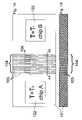
- FIGS. 1A and 1Bshow a silicon substrate 101 including chip A occupying region 102 , chip B occupying region 103 and a thermal barrier 104 separating the two regions.
- the term “chip” as used herein,generally refers to a semiconductor wafer mounted on the substrate 101 or alternatively to a circuit fabricated in the silicon substrate 101 .
- the thermal barrierincludes through vias 105 devised to form a maze-type structure. The maze of through-vias 105 lengthen the thermal path between chip A 102 and chip B 103 as illustrated by arrow 106 .
- FIG. 1A and 1Bshow a silicon substrate 101 including chip A occupying region 102 , chip B occupying region 103 and a thermal barrier 104 separating the two regions.
- the term “chip” as used herein,generally refers to a semiconductor wafer mounted on the substrate 101 or alternatively to a circuit fabricated in the silicon substrate 101 .
- the thermal barrierincludes through vias 105 devised to form a ma
- thermal impedanceis increased since vias 105 are poor thermal conductors and since conduction primarily occurs in the solid portion of maze 104 as indicated by the arrow 106 .
- FIG. 1Bshows a cross sectional view of substrate 101 having through vias 105 formed thereon.
- thermal isolationmay be enhanced by lengthening the conductive thermal path.
- through-vias 105is not limited to simple rectangles.
- FIG. 2shows a different maze layout.
- maze 204comprises a zigzag of through-vias 205 .
- the shape, width and length of vias 205is optimized to increase the thermal impedance.
- a layer of a thermally insulating material 206(such as SiO 2 ) may be formed on the top surface of substrate 201 and wires 207 may be formed in layer 206 .
- Layer 206 and wiring 207may be fabricated prior to etching through wafer vias 205 .
- Through-vias 205may be etched from the bottom surface of the wafer (the surface not containing the circuit).
- Layer 206may be fabricated after trenches 205 are made by laminating a solid sheet of a dielectric material such as polyimide.
- FIG. 3shows a cross-sectional view of substrate 301 which includes chip A 302 and chip B 303 .
- the chipsare thermally isolated by a thermal barrier 304 formed by a maze of thermal-vias 305 .
- Chip A 302is cooled by heat sink 306 .
- the heat sink's operationis enhanced by a set of thermally conducting fingers 307 .
- Fingers 307extend from heat sink 306 at the bottom of substrate 301 to the top'surface but (optionally) do not break through the substrate's top surface. Fingers 307 may be made by drilling a set of trenches and then filling the trenches with a thermal conductor such as copper.
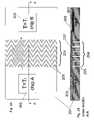
- FIG. 4shows another method for cooling the chip surface according to another embodiment of the disclosure. More specifically, FIG. 4 illustrates cooling of hot areas in an SOI chip by a copper heat sink with copper filled trenches.
- substrate 401includes BOX layer 402 , SOI film 403 and circuit with hot spots 404 .
- the hot spots 404are typically circuits in a chip that dissipate more power and thus require additional cooling.
- Cooling fingers 406are formed under the hot spots to facilitate heat conduction from hot spot 404 to heat sink 405 . Fingers 406 may be made by etching trenches from the backside of substrate 401 and using BOX layer 402 as a stop etch layer. The trenches may optionally be filled with a good heat conductor material such as copper.
- FIGS. 5A–5Cillustrate x-sectional views of the different embodiments of the disclosure.
- FIG. 5Ashows an embodiment similar to that disclosed with reference to FIGS. 1A–1B ; namely, substrate 500 having chip A and chip B separated by through vias acting as a thermal barrier.
- FIG. 5Bshow substrate 501 including chip A 502 , chip B 503 and thermal barrier 504 .
- the thermal barrierincludes top trenches 505 A and bottom trenches 505 B formed on the top and bottom surfaces of the substrate, respectively. It can be readily seen that vias 505 A and 505 B overlap over a portion of substrate 501 thereby lengthening the thermal conduction path. Some or all of the trenches may be filled with a thermally non-conductive material. As discussed in relation with FIG.
- the thermal pathis lengthen since heat is conducted in an up/down pattern in order to transmit across the trenched area 504 .
- the traversingmay be combined with the zigzag flow imposed by a maze architecture as discussed earlier to obtain an even greater thermal impedance.
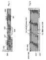
- FIG. 5Cshows substrate 511 including chip A 512 and chip B 513 separated by thermal barrier 514 .
- Thermal barrier 514includes a maze of through-vias 516 and cavity 517 . Thermal impedance is increased since through vias are formed in a thinned portion of the substrate.
- the structuremay be formed by first etching (optionally, from the back side of the substrate) a cavity 517 and then etching through-vias 516 from the top surface.
- FIGS. 6A–6Cshow another embodiment of the disclosure where a thermal barrier between chip A 602 and chip B 603 is formed by fully etching a portion of the substrate that thermally connects the two chips.
- a thermally insulating handle substrate 604is attached to substrate 601 having thereon chip A 602 and chip B 603 .
- Substrate 601may be thinned to a specified thickness. For example, a 200 mm Si substrate can be thinned down to about 20 microns by grinding and polishing.
- substrate 601is an SOI substrate in which chips A 602 and chip B 603 are formed in a SOI film over a buried oxide layer, the thinning process may be much more aggressive.
- substrate 601is first ground down to a thickness of about 20 microns.
- the substrate's siliconis then selectively etched, with the etch terminating on the buried oxide layer (not shown.)
- An example of suitable silicon etchant that is selective to silicon dioxideis TMAH (tetramethylammonium hydroxide.) This process allows thinning substrate 601 down to the thickness of the SOI film (i.e., about 0.1 micron in conventional CMOS technology.)
- thermal barrier 605is formed by etching the portion of the thinned substrate that thermally connect chip A 602 and chip B 603 .
- the etchingforms two regions 606 and 607 within the original substrate 601 ; these regions are thermally isolated. Separate heat sinks 608 and 609 are attached to the isolated substrate regions as shown in FIG. 6C .
- the handle wafer 604may include electrical traces so that chip A 602 can electrically communicate with chip B 603 .
- These wiresare typically thin enough and sparse enough to not be a significant thermal conductor between the two chips.
- the wiresare embedded in an insulator such as oxide formed on the original substrate 601 prior to bonding.
- FIGS. 7A–7Fillustrate a process for forming a thermal barrier according to another embodiment of the disclosure. More specifically, FIGS. 7A–7F illustrate a process for fabricating a thermal barrier having a trench filled with a thermally non-conductive material.
- wafer 701such as a silicon wafer is provided.
- step 2FIG. 7B
- the wafer's undersideis attached to handle wafer 702 and mask 703 is deposited and patterned to define the location of the thermal barrier.
- step 3FIG. 7C
- trench 704is etched in the substrate. As shown, the trench bottom reaches the handle wafer 702 .
- step 4FIG.
- trench 704is filled with a thermally non-conductive material 705 (“the fill material”).
- the fill materialinclude polymer, oxides, nitrides, porous films and air.
- the structureis planarized and mask 703 is removed.
- handle wafer 702is removed and the structure is sustained due to the adhering nature of the fill material. Filling the trench enables placing electrical wires across the two thermally isolated regions of the wafer.
- FIGS. 8A–8Fillustrate the process steps for forming a thermal barrier according to another embodiment of the disclosure. Specifically, FIGS. 8A–8F illustrate a variation of the process flow shown in FIGS. 7A–7F where the handle wafer is eliminated.
- step 1wafer 801 is provided.
- step 2FIG. 8B
- mask 803is deposited and patterned to define the location of the thermal barrier.
- step 3FIG. 8C
- a trench 804is etched in the substrate 801 . The trench does not break through the wafer, but leaves membrane of silicon 802 at the bottom of the trench.
- trench 804is filled with thermally non-conductive material 805 .
- step 5FIG.
- step 6the underside of wafer 801 is polished (or etched) to remove membrane 802 .
- Etching of trench 804may be implemented, for example, by using anisotropic silicon etchant such as potassium hydroxide (KOH). When such etchant is used mask 803 opening will also determine the depth of the trench since the etch will conventionally stop when the crystallographic ⁇ 111 > planes are exposed.
- anisotropic silicon etchantsuch as potassium hydroxide (KOH).
- FIGS. 9A–9Cshow top and cross-sectional views of an electromagnetic shield formed between two regions by a construction of through or embedded vias.
- a top viewis shown in FIG. 9A where, vias 901 of desired dimensions are etched into a substrate (not shown) forming a boundary around the region of interest (e.g., a thermally sensitive chip) to provide electromagnetic shielding.
- region of intereste.g., a thermally sensitive chip
- vias 901are shown to be formed around region A to isolate region A from region B in FIG. 9A .
- the number of regions and the formation of via shieldsmay vary in shape and size without departing from the principles of the disclosure.
- Vias 901may be formed, for example, by Reactive Ion Etching (“RIE”) or other chemically known methods.
- RIEReactive Ion Etching
- FIG. 9Bshows a cross-sectional view of the via shield structure where vias 901 are shown to continue through the substrate.
- FIG. 9Cshows a cross-sectional view of the via shield structure where the vias are shown to be embedded within the substrate.
- the viasmay be fully or partially filled with a conductive material including copper, nickel, conductive pastes, etc. Where the via is partially filled, the remaining volume of the via may be filled with a conductive material, a non-conductive material or left unfilled.
- FIGS. 10A–10Dillustrate closed or open loop trenches forming an electromagnetic shield between two regions of a substrate.
- a top view of a closed loop trench and an open loop trenchis shown in FIGS. 10A and 10B , respectively, where a trench of desired dimensions is etched into a substrate forming a boundary around the region of interest to provide electromagnetic shielding.
- trench 1001is shown to have been formed around region A, isolating this region from region B in FIGS. 10A and 10B .
- Region Bis isolated from Region A vis-à-vis the open loop trench 1001 .
- the trenchmay be formed by Reactive Ion Etching or other conventional methods.
- FIG. 10Cshows a cross-sectional view of trench shield 1001 where the trench is shown to extend through the substrate.
- FIG. 10Dshows a cross-sectional view of the trench shield structure where trench 1001 is shown to be embedded within the substrate.
- the trenchmay be fully or partially filled with a conductive material such as copper, nickel, conductive pastes, etc.
- FIGS. 11A–11Cshow the presence of electrical contacts to the via shield or the trench shield structures by using subsequent levels of wiring built onto the chip or the substrate.
- the electrical contactsmay be biased at a desired potential to provide an effective electromagnetic shield between the regions of interest.
- the electrical contactsmay be grounded to avoid electromagnetic interference and improve shielding.
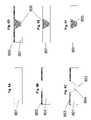
- FIG. 11Ashows Region A in electromagnetic communication with voltage source which may be ground.
- Each of trenches 1104are shown to communicate with source 1103 or ground 1105 .
- the electromagnetic shield of FIG. 11Amay be similar to that shown in FIG. 9 .
- FIG. 11Bshows an electromagnetic shield provided by trench 1102 in communication with voltage source 1103 or ground 1105 .
- FIG. 11Billustrates the structure of FIG. 10(B) having open-loop trench 1102 coupled to voltage source 1103 or optionally to ground 1105 .
- the electromagnetic shield illustrated in FIGS. 9 and 10may be combined with a thermal shield as shown in FIGS. 1–5 to further thermal and electromagnetic isolation.
- the resulting structuremay have one or more electromagnetic shields interposed, at least partially, between the regions A and B, as well as a barrier region having defining a thermal path between these regions.
- the electromagnetic shieldmay optionally be coupled to a voltage source or ground.
Landscapes
- Engineering & Computer Science (AREA)
- Physics & Mathematics (AREA)
- Power Engineering (AREA)
- Condensed Matter Physics & Semiconductors (AREA)
- General Physics & Mathematics (AREA)
- Computer Hardware Design (AREA)
- Microelectronics & Electronic Packaging (AREA)
- Toxicology (AREA)
- Electromagnetism (AREA)
- Health & Medical Sciences (AREA)
- Chemical & Material Sciences (AREA)
- Materials Engineering (AREA)
- Internal Circuitry In Semiconductor Integrated Circuit Devices (AREA)
Abstract
Description
Claims (6)
Priority Applications (1)
| Application Number | Priority Date | Filing Date | Title |
|---|---|---|---|
| US10/872,451US7033927B2 (en) | 2004-06-22 | 2004-06-22 | Apparatus and method for thermal isolation, circuit cooling and electromagnetic shielding of a wafer |
Applications Claiming Priority (1)
| Application Number | Priority Date | Filing Date | Title |
|---|---|---|---|
| US10/872,451US7033927B2 (en) | 2004-06-22 | 2004-06-22 | Apparatus and method for thermal isolation, circuit cooling and electromagnetic shielding of a wafer |
Publications (2)
| Publication Number | Publication Date |
|---|---|
| US20050282381A1 US20050282381A1 (en) | 2005-12-22 |
| US7033927B2true US7033927B2 (en) | 2006-04-25 |
Family
ID=35481170
Family Applications (1)
| Application Number | Title | Priority Date | Filing Date |
|---|---|---|---|
| US10/872,451Expired - LifetimeUS7033927B2 (en) | 2004-06-22 | 2004-06-22 | Apparatus and method for thermal isolation, circuit cooling and electromagnetic shielding of a wafer |
Country Status (1)
| Country | Link |
|---|---|
| US (1) | US7033927B2 (en) |
Cited By (30)
| Publication number | Priority date | Publication date | Assignee | Title |
|---|---|---|---|---|
| US20050260802A1 (en)* | 2004-04-07 | 2005-11-24 | Andrea Pizzarulli | SOI circuit having reduced crosstalk interference and a method for forming the same |
| US20060177999A1 (en)* | 2005-02-10 | 2006-08-10 | Micron Technology, Inc. | Microelectronic workpieces and methods for forming interconnects in microelectronic workpieces |
| US20060199363A1 (en)* | 2004-06-29 | 2006-09-07 | Micron Technology, Inc. | Microelectronic devices and methods for forming interconnects in microelectronic devices |
| US20070015346A1 (en)* | 2004-06-14 | 2007-01-18 | International Business Machines Corporation | Mixed orientation and mixed material semiconductor-on-insulator wafer |
| US20080050911A1 (en)* | 2006-08-28 | 2008-02-28 | Micron Technology, Inc. | Microfeature workpieces having conductive interconnect structures formed by chemically reactive processes, and associated systems and methods |
| US20080116541A1 (en)* | 2006-11-20 | 2008-05-22 | International Business Machines Corporation | Structure for integrating an rf shield structure in a carrier substrate |
| US7413979B2 (en) | 2003-11-13 | 2008-08-19 | Micron Technology, Inc. | Methods for forming vias in microelectronic devices, and methods for packaging microelectronic devices |
| US7425499B2 (en) | 2004-08-24 | 2008-09-16 | Micron Technology, Inc. | Methods for forming interconnects in vias and microelectronic workpieces including such interconnects |
| US7435913B2 (en) | 2004-08-27 | 2008-10-14 | Micron Technology, Inc. | Slanted vias for electrical circuits on circuit boards and other substrates |
| US7589008B2 (en) | 2004-12-30 | 2009-09-15 | Micron Technology, Inc. | Methods for forming interconnects in microelectronic workpieces and microelectronic workpieces formed using such methods |
| US7622377B2 (en) | 2005-09-01 | 2009-11-24 | Micron Technology, Inc. | Microfeature workpiece substrates having through-substrate vias, and associated methods of formation |
| US7683458B2 (en) | 2004-09-02 | 2010-03-23 | Micron Technology, Inc. | Through-wafer interconnects for photoimager and memory wafers |
| US20100078771A1 (en)* | 2008-09-30 | 2010-04-01 | Hans-Joachim Barth | On-Chip RF Shields with Through Substrate Conductors |
| US20100078776A1 (en)* | 2008-09-30 | 2010-04-01 | Hans-Joachim Barth | On-Chip RF Shields with Backside Redistribution Lines |
| US20100078779A1 (en)* | 2008-09-30 | 2010-04-01 | Hans-Joachim Barth | System on a Chip with On-Chip RF Shield |
| US20100078777A1 (en)* | 2008-09-30 | 2010-04-01 | Hans-Joachim Barth | On-Chip Radio Frequency Shield with Interconnect Metallization |
| US20100078778A1 (en)* | 2008-09-30 | 2010-04-01 | Hans-Joachim Barth | On-Chip RF Shields with Front Side Redistribution Lines |
| US7749899B2 (en) | 2006-06-01 | 2010-07-06 | Micron Technology, Inc. | Microelectronic workpieces and methods and systems for forming interconnects in microelectronic workpieces |
| US7795134B2 (en) | 2005-06-28 | 2010-09-14 | Micron Technology, Inc. | Conductive interconnect structures and formation methods using supercritical fluids |
| US7830018B2 (en) | 2007-08-31 | 2010-11-09 | Micron Technology, Inc. | Partitioned through-layer via and associated systems and methods |
| US7863187B2 (en) | 2005-09-01 | 2011-01-04 | Micron Technology, Inc. | Microfeature workpieces and methods for forming interconnects in microfeature workpieces |
| US7884015B2 (en) | 2007-12-06 | 2011-02-08 | Micron Technology, Inc. | Methods for forming interconnects in microelectronic workpieces and microelectronic workpieces formed using such methods |
| US7902643B2 (en) | 2006-08-31 | 2011-03-08 | Micron Technology, Inc. | Microfeature workpieces having interconnects and conductive backplanes, and associated systems and methods |
| US7915736B2 (en) | 2005-09-01 | 2011-03-29 | Micron Technology, Inc. | Microfeature workpieces and methods for forming interconnects in microfeature workpieces |
| US8084866B2 (en) | 2003-12-10 | 2011-12-27 | Micron Technology, Inc. | Microelectronic devices and methods for filling vias in microelectronic devices |
| US20120146193A1 (en)* | 2010-12-13 | 2012-06-14 | Io Semiconductor, Inc. | Thermal Conduction Paths for Semiconductor Structures |
| WO2013033654A1 (en)* | 2011-08-31 | 2013-03-07 | De Rochemont L Pierre | Fully integrated thermoelectric devices and their application to aerospace de-icing systems |
| US8536485B2 (en) | 2004-05-05 | 2013-09-17 | Micron Technology, Inc. | Systems and methods for forming apertures in microfeature workpieces |
| US8889548B2 (en) | 2008-09-30 | 2014-11-18 | Infineon Technologies Ag | On-chip RF shields with backside redistribution lines |
| US8912574B2 (en) | 2010-12-14 | 2014-12-16 | International Business Machines Corporation | Device isolation with improved thermal conductivity |
Families Citing this family (13)
| Publication number | Priority date | Publication date | Assignee | Title |
|---|---|---|---|---|
| US7692148B2 (en)* | 2005-01-26 | 2010-04-06 | Analog Devices, Inc. | Thermal sensor with thermal barrier |
| US7786546B2 (en)* | 2005-02-25 | 2010-08-31 | United Microelectronics Corp. | System-on-chip with shield rings for shielding functional blocks therein from electromagnetic interference |
| US7170144B2 (en)* | 2005-02-25 | 2007-01-30 | United Microelectronics Corp. | System-on-chip with shield rings for shielding functional blocks therein from electromagnetic interference |
| US7427803B2 (en)* | 2006-09-22 | 2008-09-23 | Taiwan Semiconductor Manufacturing Company, Ltd. | Electromagnetic shielding using through-silicon vias |
| US7550853B2 (en)* | 2007-10-10 | 2009-06-23 | Itt Manufacturing Enterprises, Inc. | Electrical isolation of monolithic circuits using a conductive through-hole in the substrate |
| US8232625B2 (en)* | 2009-03-26 | 2012-07-31 | International Business Machines Corporation | ESD network circuit with a through wafer via structure and a method of manufacture |
| JP5218657B2 (en)* | 2009-06-15 | 2013-06-26 | 富士通オプティカルコンポーネンツ株式会社 | Optical module |
| US8054597B2 (en)* | 2009-06-23 | 2011-11-08 | International Business Machines Corporation | Electrostatic discharge structures and methods of manufacture |
| KR102253473B1 (en)* | 2014-09-30 | 2021-05-18 | 삼성전기주식회사 | Circuit board |
| US10002838B2 (en) | 2016-06-22 | 2018-06-19 | Qualcomm Incorporated | Method and apparatus for back-biased switch transistors |
| US9755029B1 (en) | 2016-06-22 | 2017-09-05 | Qualcomm Incorporated | Switch device performance improvement through multisided biased shielding |
| CN109037159B (en)* | 2018-08-15 | 2024-05-10 | 深圳市金誉半导体股份有限公司 | Packaging structure and manufacturing method of power chip |
| US11049788B2 (en)* | 2019-10-18 | 2021-06-29 | Microsoft Technology Licensing, Llc | Integrated circuit chip device with thermal control |
Citations (2)
| Publication number | Priority date | Publication date | Assignee | Title |
|---|---|---|---|---|
| US6100199A (en) | 1998-01-13 | 2000-08-08 | International Business Machines Corporation | Embedded thermal conductors for semiconductor chips |
| US20020033189A1 (en)* | 2000-09-18 | 2002-03-21 | Chris Macris | Heat dissipating silicon-on-insulator structures |
- 2004
- 2004-06-22USUS10/872,451patent/US7033927B2/ennot_activeExpired - Lifetime
Patent Citations (2)
| Publication number | Priority date | Publication date | Assignee | Title |
|---|---|---|---|---|
| US6100199A (en) | 1998-01-13 | 2000-08-08 | International Business Machines Corporation | Embedded thermal conductors for semiconductor chips |
| US20020033189A1 (en)* | 2000-09-18 | 2002-03-21 | Chris Macris | Heat dissipating silicon-on-insulator structures |
Non-Patent Citations (3)
| Title |
|---|
| Soh, H.T., et al., "Ultra-Low Resistance, Through-Wafer VIA (TWV) Technology and its Applications in Three Dimensional Structures on Silicon," Japanese Journal of Applied Physics, vol. 38, 1999. |
| Wu, j., et al., "A High Aspect Ratio Silicon Substrate-Via Technnology and Applications: Through-Wafer Interconnects for Power and Ground and Faraday Cages for SOC Isolation," IEDM, 2000. |
| Wu, J.H., et al., "A Faraday Cage Isolation Structure for Substrate Crosstalk Suppression," IEEE Microwave and Wireless Components Letters, vol. 11, No. 10, Oct. 2001. |
Cited By (76)
| Publication number | Priority date | Publication date | Assignee | Title |
|---|---|---|---|---|
| US7413979B2 (en) | 2003-11-13 | 2008-08-19 | Micron Technology, Inc. | Methods for forming vias in microelectronic devices, and methods for packaging microelectronic devices |
| US7759800B2 (en) | 2003-11-13 | 2010-07-20 | Micron Technology, Inc. | Microelectronics devices, having vias, and packaged microelectronic devices having vias |
| US9653420B2 (en) | 2003-11-13 | 2017-05-16 | Micron Technology, Inc. | Microelectronic devices and methods for filling vias in microelectronic devices |
| US11177175B2 (en) | 2003-12-10 | 2021-11-16 | Micron Technology, Inc. | Microelectronic devices and methods for filling vias in microelectronic devices |
| US8084866B2 (en) | 2003-12-10 | 2011-12-27 | Micron Technology, Inc. | Microelectronic devices and methods for filling vias in microelectronic devices |
| US8748311B2 (en) | 2003-12-10 | 2014-06-10 | Micron Technology, Inc. | Microelectronic devices and methods for filing vias in microelectronic devices |
| US20050260802A1 (en)* | 2004-04-07 | 2005-11-24 | Andrea Pizzarulli | SOI circuit having reduced crosstalk interference and a method for forming the same |
| US8536485B2 (en) | 2004-05-05 | 2013-09-17 | Micron Technology, Inc. | Systems and methods for forming apertures in microfeature workpieces |
| US10010977B2 (en) | 2004-05-05 | 2018-07-03 | Micron Technology, Inc. | Systems and methods for forming apertures in microfeature workpieces |
| US8664562B2 (en) | 2004-05-05 | 2014-03-04 | Micron Technology, Inc. | Systems and methods for forming apertures in microfeature workpieces |
| US8686313B2 (en) | 2004-05-05 | 2014-04-01 | Micron Technology, Inc. | System and methods for forming apertures in microfeature workpieces |
| US9452492B2 (en) | 2004-05-05 | 2016-09-27 | Micron Technology, Inc. | Systems and methods for forming apertures in microfeature workpieces |
| US20070015346A1 (en)* | 2004-06-14 | 2007-01-18 | International Business Machines Corporation | Mixed orientation and mixed material semiconductor-on-insulator wafer |
| US7449767B2 (en) | 2004-06-14 | 2008-11-11 | International Business Machines Corporation | Mixed orientation and mixed material semiconductor-on-insulator wafer |
| US7531453B2 (en) | 2004-06-29 | 2009-05-12 | Micron Technology, Inc. | Microelectronic devices and methods for forming interconnects in microelectronic devices |
| US20060199363A1 (en)* | 2004-06-29 | 2006-09-07 | Micron Technology, Inc. | Microelectronic devices and methods for forming interconnects in microelectronic devices |
| US7829976B2 (en) | 2004-06-29 | 2010-11-09 | Micron Technology, Inc. | Microelectronic devices and methods for forming interconnects in microelectronic devices |
| US7329943B2 (en) | 2004-06-29 | 2008-02-12 | Micron Technology, Inc. | Microelectronic devices and methods for forming interconnects in microelectronic devices |
| US20080138973A1 (en)* | 2004-06-29 | 2008-06-12 | Micron Technology, Inc. | Microelectronic devices and methods for forming interconnects in microelectronic devices |
| US7425499B2 (en) | 2004-08-24 | 2008-09-16 | Micron Technology, Inc. | Methods for forming interconnects in vias and microelectronic workpieces including such interconnects |
| US20090008144A1 (en)* | 2004-08-27 | 2009-01-08 | Micron Technology, Inc. | Slanted vias for electrical circuits on circuit boards and other substrates |
| US8322031B2 (en) | 2004-08-27 | 2012-12-04 | Micron Technology, Inc. | Method of manufacturing an interposer |
| US7435913B2 (en) | 2004-08-27 | 2008-10-14 | Micron Technology, Inc. | Slanted vias for electrical circuits on circuit boards and other substrates |
| US8669179B2 (en) | 2004-09-02 | 2014-03-11 | Micron Technology, Inc. | Through-wafer interconnects for photoimager and memory wafers |
| US7956443B2 (en) | 2004-09-02 | 2011-06-07 | Micron Technology, Inc. | Through-wafer interconnects for photoimager and memory wafers |
| US8502353B2 (en) | 2004-09-02 | 2013-08-06 | Micron Technology, Inc. | Through-wafer interconnects for photoimager and memory wafers |
| US7683458B2 (en) | 2004-09-02 | 2010-03-23 | Micron Technology, Inc. | Through-wafer interconnects for photoimager and memory wafers |
| US9214391B2 (en) | 2004-12-30 | 2015-12-15 | Micron Technology, Inc. | Methods for forming interconnects in microelectronic workpieces and microelectronic workpieces formed using such methods |
| US7589008B2 (en) | 2004-12-30 | 2009-09-15 | Micron Technology, Inc. | Methods for forming interconnects in microelectronic workpieces and microelectronic workpieces formed using such methods |
| US20060177999A1 (en)* | 2005-02-10 | 2006-08-10 | Micron Technology, Inc. | Microelectronic workpieces and methods for forming interconnects in microelectronic workpieces |
| US8008192B2 (en) | 2005-06-28 | 2011-08-30 | Micron Technology, Inc. | Conductive interconnect structures and formation methods using supercritical fluids |
| US7795134B2 (en) | 2005-06-28 | 2010-09-14 | Micron Technology, Inc. | Conductive interconnect structures and formation methods using supercritical fluids |
| US9293367B2 (en) | 2005-06-28 | 2016-03-22 | Micron Technology, Inc. | Conductive interconnect structures and formation methods using supercritical fluids |
| US7863187B2 (en) | 2005-09-01 | 2011-01-04 | Micron Technology, Inc. | Microfeature workpieces and methods for forming interconnects in microfeature workpieces |
| US12014958B2 (en) | 2005-09-01 | 2024-06-18 | Micron Technology, Inc. | Microfeature workpieces and methods for forming interconnects in microfeature workpieces |
| US11476160B2 (en) | 2005-09-01 | 2022-10-18 | Micron Technology, Inc. | Microfeature workpieces and methods for forming interconnects in microfeature workpieces |
| US7915736B2 (en) | 2005-09-01 | 2011-03-29 | Micron Technology, Inc. | Microfeature workpieces and methods for forming interconnects in microfeature workpieces |
| US7622377B2 (en) | 2005-09-01 | 2009-11-24 | Micron Technology, Inc. | Microfeature workpiece substrates having through-substrate vias, and associated methods of formation |
| US7749899B2 (en) | 2006-06-01 | 2010-07-06 | Micron Technology, Inc. | Microelectronic workpieces and methods and systems for forming interconnects in microelectronic workpieces |
| US20080050911A1 (en)* | 2006-08-28 | 2008-02-28 | Micron Technology, Inc. | Microfeature workpieces having conductive interconnect structures formed by chemically reactive processes, and associated systems and methods |
| US7629249B2 (en) | 2006-08-28 | 2009-12-08 | Micron Technology, Inc. | Microfeature workpieces having conductive interconnect structures formed by chemically reactive processes, and associated systems and methods |
| US8610279B2 (en) | 2006-08-28 | 2013-12-17 | Micron Technologies, Inc. | Microfeature workpieces having conductive interconnect structures formed by chemically reactive processes, and associated systems and methods |
| US7973411B2 (en) | 2006-08-28 | 2011-07-05 | Micron Technology, Inc. | Microfeature workpieces having conductive interconnect structures formed by chemically reactive processes, and associated systems and methods |
| US7902643B2 (en) | 2006-08-31 | 2011-03-08 | Micron Technology, Inc. | Microfeature workpieces having interconnects and conductive backplanes, and associated systems and methods |
| US9570350B2 (en) | 2006-08-31 | 2017-02-14 | Micron Technology, Inc. | Microfeature workpieces having interconnects and conductive backplanes, and associated systems and methods |
| US9099539B2 (en) | 2006-08-31 | 2015-08-04 | Micron Technology, Inc. | Microfeature workpieces having interconnects and conductive backplanes, and associated systems and methods |
| US20080116541A1 (en)* | 2006-11-20 | 2008-05-22 | International Business Machines Corporation | Structure for integrating an rf shield structure in a carrier substrate |
| US7830018B2 (en) | 2007-08-31 | 2010-11-09 | Micron Technology, Inc. | Partitioned through-layer via and associated systems and methods |
| US8367538B2 (en) | 2007-08-31 | 2013-02-05 | Micron Technology, Inc. | Partitioned through-layer via and associated systems and methods |
| US8536046B2 (en) | 2007-08-31 | 2013-09-17 | Micron Technology | Partitioned through-layer via and associated systems and methods |
| US8247907B2 (en) | 2007-12-06 | 2012-08-21 | Micron Technology, Inc. | Methods for forming interconnects in microelectronic workpieces and microelectronic workpieces formed using such methods |
| US9281241B2 (en) | 2007-12-06 | 2016-03-08 | Micron Technology, Inc. | Methods for forming interconnects in microelectronic workpieces and microelectronic workpieces formed using such methods |
| US7884015B2 (en) | 2007-12-06 | 2011-02-08 | Micron Technology, Inc. | Methods for forming interconnects in microelectronic workpieces and microelectronic workpieces formed using such methods |
| US8617929B2 (en) | 2008-09-30 | 2013-12-31 | Infineon Technologies Ag | On-Chip RF shields with front side redistribution lines |
| US8178953B2 (en) | 2008-09-30 | 2012-05-15 | Infineon Technologies Ag | On-chip RF shields with front side redistribution lines |
| US20100078777A1 (en)* | 2008-09-30 | 2010-04-01 | Hans-Joachim Barth | On-Chip Radio Frequency Shield with Interconnect Metallization |
| US20100078779A1 (en)* | 2008-09-30 | 2010-04-01 | Hans-Joachim Barth | System on a Chip with On-Chip RF Shield |
| US8748287B2 (en) | 2008-09-30 | 2014-06-10 | Infineon Technologies Ag | System on a chip with on-chip RF shield |
| US20100078776A1 (en)* | 2008-09-30 | 2010-04-01 | Hans-Joachim Barth | On-Chip RF Shields with Backside Redistribution Lines |
| US8889548B2 (en) | 2008-09-30 | 2014-11-18 | Infineon Technologies Ag | On-chip RF shields with backside redistribution lines |
| US7936052B2 (en) | 2008-09-30 | 2011-05-03 | Infineon Technologies Ag | On-chip RF shields with backside redistribution lines |
| US8536683B2 (en) | 2008-09-30 | 2013-09-17 | Infineon Technologies Ag | System on a chip with on-chip RF shield |
| US20100078771A1 (en)* | 2008-09-30 | 2010-04-01 | Hans-Joachim Barth | On-Chip RF Shields with Through Substrate Conductors |
| US7948064B2 (en) | 2008-09-30 | 2011-05-24 | Infineon Technologies Ag | System on a chip with on-chip RF shield |
| US20110201175A1 (en)* | 2008-09-30 | 2011-08-18 | Hans-Joachim Barth | System on a Chip with On-Chip RF Shield |
| US9390973B2 (en) | 2008-09-30 | 2016-07-12 | Infineon Technologies Ag | On-chip RF shields with backside redistribution lines |
| US8063469B2 (en) | 2008-09-30 | 2011-11-22 | Infineon Technologies Ag | On-chip radio frequency shield with interconnect metallization |
| US8169059B2 (en)* | 2008-09-30 | 2012-05-01 | Infineon Technologies Ag | On-chip RF shields with through substrate conductors |
| US20100078778A1 (en)* | 2008-09-30 | 2010-04-01 | Hans-Joachim Barth | On-Chip RF Shields with Front Side Redistribution Lines |
| US20120146193A1 (en)* | 2010-12-13 | 2012-06-14 | Io Semiconductor, Inc. | Thermal Conduction Paths for Semiconductor Structures |
| US8466054B2 (en)* | 2010-12-13 | 2013-06-18 | Io Semiconductor, Inc. | Thermal conduction paths for semiconductor structures |
| US9564508B2 (en) | 2010-12-14 | 2017-02-07 | Globalfoundries Inc. | Device isolation with improved thermal conductivity |
| US8912574B2 (en) | 2010-12-14 | 2014-12-16 | International Business Machines Corporation | Device isolation with improved thermal conductivity |
| US9490414B2 (en) | 2011-08-31 | 2016-11-08 | L. Pierre de Rochemont | Fully integrated thermoelectric devices and their application to aerospace de-icing systems |
| US10593855B2 (en) | 2011-08-31 | 2020-03-17 | L. Pierre de Rochemont | Fully integrated thermoelectric devices and their application to aerospace de-icing systems |
| WO2013033654A1 (en)* | 2011-08-31 | 2013-03-07 | De Rochemont L Pierre | Fully integrated thermoelectric devices and their application to aerospace de-icing systems |
Also Published As
| Publication number | Publication date |
|---|---|
| US20050282381A1 (en) | 2005-12-22 |
Similar Documents
| Publication | Publication Date | Title |
|---|---|---|
| US7033927B2 (en) | Apparatus and method for thermal isolation, circuit cooling and electromagnetic shielding of a wafer | |
| US5753529A (en) | Surface mount and flip chip technology for total integrated circuit isolation | |
| JP5048230B2 (en) | Semiconductor device and manufacturing method thereof | |
| KR100656218B1 (en) | Systems on Packages Fabricated on Semiconductor or Dielectric Wafers | |
| JP4472340B2 (en) | Semiconductor device using low dielectric constant material film and manufacturing method thereof | |
| US8466054B2 (en) | Thermal conduction paths for semiconductor structures | |
| US5767578A (en) | Surface mount and flip chip technology with diamond film passivation for total integated circuit isolation | |
| US5998292A (en) | Method for making three dimensional circuit integration | |
| KR101018419B1 (en) | Single Mask Via Method and Device | |
| KR100294747B1 (en) | Method for forming vertically connected semiconductor parts | |
| JP4979213B2 (en) | Circuit board, circuit board manufacturing method, and circuit device | |
| US6221751B1 (en) | Wafer fabrication of die-bottom contacts for electronic devices | |
| JP5209301B2 (en) | Technology and RF circuit design to reduce substrate crosstalk for mixed signals | |
| JP2005150717A (en) | Integrated circuit equipment and its manufacturing method | |
| WO1995031006A1 (en) | Surface mount and flip chip technology | |
| US7105910B2 (en) | Semiconductor device having SOI construction | |
| JP2002050742A (en) | Semiconductor device and production method therefor | |
| US6002154A (en) | High-frequency MOSFET | |
| JP4678720B2 (en) | Circuit board and manufacturing method thereof, semiconductor device and manufacturing method thereof | |
| JP5025922B2 (en) | Circuit board, method for manufacturing circuit board, and semiconductor device | |
| US7898052B2 (en) | Component with a semiconductor junction and method for the production thereof | |
| CN100505300C (en) | Semiconductor device and manufacturing method thereof | |
| JP2007042824A (en) | Electronic circuit device and manufacturing method thereof | |
| CN117524982A (en) | Manufacturing method of chip structure and chip structure | |
| CN115394737A (en) | Chip package and method for manufacturing the same |
Legal Events
| Date | Code | Title | Description |
|---|---|---|---|
| AS | Assignment | Owner name:INTERNATIONAL BUSINESS MACHINES CORPORATION, NEW Y Free format text:ASSIGNMENT OF ASSIGNORS INTEREST;ASSIGNORS:COHEN, GUY M.;EDELSTEIN, DANIEL C.;JENKINS, KEITH A.;AND OTHERS;REEL/FRAME:016288/0985;SIGNING DATES FROM 20040621 TO 20040628 | |
| STCF | Information on status: patent grant | Free format text:PATENTED CASE | |
| FPAY | Fee payment | Year of fee payment:4 | |
| REMI | Maintenance fee reminder mailed | ||
| AS | Assignment | Owner name:TWITTER, INC., CALIFORNIA Free format text:ASSIGNMENT OF ASSIGNORS INTEREST;ASSIGNOR:INTERNATIONAL BUSINESS MACHINES CORPORATION;REEL/FRAME:032075/0404 Effective date:20131230 | |
| FPAY | Fee payment | Year of fee payment:8 | |
| SULP | Surcharge for late payment | Year of fee payment:7 | |
| FEPP | Fee payment procedure | Free format text:MAINTENANCE FEE REMINDER MAILED (ORIGINAL EVENT CODE: REM.) | |
| FEPP | Fee payment procedure | Free format text:11.5 YR SURCHARGE- LATE PMT W/IN 6 MO, LARGE ENTITY (ORIGINAL EVENT CODE: M1556) | |
| MAFP | Maintenance fee payment | Free format text:PAYMENT OF MAINTENANCE FEE, 12TH YEAR, LARGE ENTITY (ORIGINAL EVENT CODE: M1553) Year of fee payment:12 | |
| AS | Assignment | Owner name:MORGAN STANLEY SENIOR FUNDING, INC., MARYLAND Free format text:SECURITY INTEREST;ASSIGNOR:TWITTER, INC.;REEL/FRAME:062079/0677 Effective date:20221027 Owner name:MORGAN STANLEY SENIOR FUNDING, INC., MARYLAND Free format text:SECURITY INTEREST;ASSIGNOR:TWITTER, INC.;REEL/FRAME:061804/0086 Effective date:20221027 Owner name:MORGAN STANLEY SENIOR FUNDING, INC., MARYLAND Free format text:SECURITY INTEREST;ASSIGNOR:TWITTER, INC.;REEL/FRAME:061804/0001 Effective date:20221027 | |
| AS | Assignment | Owner name:X CORP. (F/K/A TWITTER, INC.), TEXAS Free format text:RELEASE BY SECURED PARTY;ASSIGNOR:MORGAN STANLEY SENIOR FUNDING, INC.;REEL/FRAME:070670/0857 Effective date:20250220 | |
| AS | Assignment | Owner name:X CORP. (F/K/A TWITTER, INC.), TEXAS Free format text:RELEASE BY SECURED PARTY;ASSIGNOR:MORGAN STANLEY SENIOR FUNDING, INC., AS COLLATERAL AGENT;REEL/FRAME:071127/0240 Effective date:20250429 |