US7031615B2 - Optical channel selection and evaluation system - Google Patents
Optical channel selection and evaluation systemDownload PDFInfo
- Publication number
- US7031615B2 US7031615B2US09/971,970US97197001AUS7031615B2US 7031615 B2US7031615 B2US 7031615B2US 97197001 AUS97197001 AUS 97197001AUS 7031615 B2US7031615 B2US 7031615B2
- Authority
- US
- United States
- Prior art keywords
- optical
- signal
- channels
- analyzable
- optical channel
- Prior art date
- Legal status (The legal status is an assumption and is not a legal conclusion. Google has not performed a legal analysis and makes no representation as to the accuracy of the status listed.)
- Expired - Lifetime, expires
Links
- 230000003287optical effectEffects0.000titleclaimsabstractdescription185
- 238000011156evaluationMethods0.000titleclaimsdescription17
- 238000000034methodMethods0.000claimsabstractdescription16
- 238000011084recoveryMethods0.000claimsabstractdescription10
- 239000000835fiberSubstances0.000claimsdescription25
- 230000008878couplingEffects0.000claimsdescription11
- 238000010168coupling processMethods0.000claimsdescription11
- 238000005859coupling reactionMethods0.000claimsdescription11
- 230000008569processEffects0.000claimsdescription5
- 230000005540biological transmissionEffects0.000claimsdescription4
- 239000013307optical fiberSubstances0.000claims1
- 238000004891communicationMethods0.000abstractdescription12
- 238000011109contaminationMethods0.000abstractdescription3
- 238000005215recombinationMethods0.000abstract1
- 230000006798recombinationEffects0.000abstract1
- 238000012360testing methodMethods0.000description34
- 238000012544monitoring processMethods0.000description9
- 239000004020conductorSubstances0.000description8
- 238000010586diagramMethods0.000description7
- 230000008901benefitEffects0.000description3
- 238000006243chemical reactionMethods0.000description3
- 239000000284extractSubstances0.000description2
- 230000003116impacting effectEffects0.000description2
- 239000004065semiconductorSubstances0.000description2
- RYGMFSIKBFXOCR-UHFFFAOYSA-NCopperChemical compound[Cu]RYGMFSIKBFXOCR-UHFFFAOYSA-N0.000description1
- 229910052802copperInorganic materials0.000description1
- 239000010949copperSubstances0.000description1
- 230000001934delayEffects0.000description1
- RGNPBRKPHBKNKX-UHFFFAOYSA-NhexaflumuronChemical compoundC1=C(Cl)C(OC(F)(F)C(F)F)=C(Cl)C=C1NC(=O)NC(=O)C1=C(F)C=CC=C1FRGNPBRKPHBKNKX-UHFFFAOYSA-N0.000description1
- 238000003780insertionMethods0.000description1
- 230000037431insertionEffects0.000description1
- 238000009434installationMethods0.000description1
- 230000010354integrationEffects0.000description1
- 230000007246mechanismEffects0.000description1
- 229910052751metalInorganic materials0.000description1
- 239000002184metalSubstances0.000description1
- 150000002739metalsChemical class0.000description1
- 238000012986modificationMethods0.000description1
- 230000004048modificationEffects0.000description1
- 238000003012network analysisMethods0.000description1
- 238000010079rubber tappingMethods0.000description1
- 230000035945sensitivityEffects0.000description1
- 230000002463transducing effectEffects0.000description1
Images


Classifications
- H—ELECTRICITY
- H04—ELECTRIC COMMUNICATION TECHNIQUE
- H04B—TRANSMISSION
- H04B10/00—Transmission systems employing electromagnetic waves other than radio-waves, e.g. infrared, visible or ultraviolet light, or employing corpuscular radiation, e.g. quantum communication
- H04B10/07—Arrangements for monitoring or testing transmission systems; Arrangements for fault measurement of transmission systems
- H04B10/075—Arrangements for monitoring or testing transmission systems; Arrangements for fault measurement of transmission systems using an in-service signal
- H04B10/079—Arrangements for monitoring or testing transmission systems; Arrangements for fault measurement of transmission systems using an in-service signal using measurements of the data signal
- H04B10/0795—Performance monitoring; Measurement of transmission parameters
- H04B10/07955—Monitoring or measuring power
- H—ELECTRICITY
- H04—ELECTRIC COMMUNICATION TECHNIQUE
- H04B—TRANSMISSION
- H04B10/00—Transmission systems employing electromagnetic waves other than radio-waves, e.g. infrared, visible or ultraviolet light, or employing corpuscular radiation, e.g. quantum communication
- H04B10/07—Arrangements for monitoring or testing transmission systems; Arrangements for fault measurement of transmission systems
- H04B10/075—Arrangements for monitoring or testing transmission systems; Arrangements for fault measurement of transmission systems using an in-service signal
- H04B10/077—Arrangements for monitoring or testing transmission systems; Arrangements for fault measurement of transmission systems using an in-service signal using a supervisory or additional signal
Definitions
- the present inventionrelates to a circuit and system for selecting and evaluating an optical communication channel.
- the inventionrelates to an optical integrated in-line switching device for selecting a specific communication channel for evaluation.
- Communication system channelshave largely been composed of metallic conductors such as copper or other low resistance metals. Systems using such conductors have generally been relatively easy to monitor and evaluate without great disruption or intrusion into the communication channel since current flows throughout the entire conductor and portions of the conductor can be externally “tapped” with another conductor attached to the test equipment that bleeds-off a negligible amount of test current.
- Fiber conductorsunlike metallic conductors, propagate the information signal in a very longitudinally directional path. Furthermore, the information signal propagates down a very narrow internal portion of the conductor making the non-intrusive external “tapping” of the fiber impractical.
- a splitteralso known as a coupler
- a splitterin order to monitor a fiber channel, must be placed “in-line” with the fiber channel to reflect a portion of the light from the main conductive fiber channel to another conductive fiber channel that can be coupled to a network analyzer or other test equipment.
- FIG. 1a system 100 for monitoring a plurality of fiber channels 102 – 108 is depicted with a corresponding plurality of dedicated couplers 110 – 116 connecting with a corresponding plurality of dedicated test equipment 118 – 124 . While such an arrangement makes in-line testing possible, the installation of such couplers into the individual channels has been complex and tedious.
- a system and method of selecting and viewing communication traffic transmitted over an optical channel selected from among a plurality of channels without intruding upon the normal traffic of that selected channel or requiring a separate channel dedicated to monitoring and analyzingis presented.
- the system and method for selecting and analyzing the channel from among a plurality of channelsincludes an optical channel analyzing switch for selecting the channel to be monitored from among several channels and test equipment such as a network analyzer for evaluating the selected channel.
- the optical channel analyzing switchincludes an optical coupler for each of the plurality of possibly analyzed channels.
- the optical couplerreceives an input optical signal and splits the signal into two paths, a first pass-through path that provides continuous normal routing of optical channel traffic and a second analyzable output optical path that “taps” the channel and routes the input optical signal for that channel for routing to analyzer equipment when selected.
- the analyzable output optical signalis converted from an optical or light signal into an analyzable electrical signal. This conversion is performed by a receiver having an optical input and an electrical signal output.
- the optical channel analyzing switchfurther includes a multiplexor coupled on the inputs to the analyzable electrical signals of the severally available optical channels.
- the multiplexoris preferably computer controlled to select an output from among one of the potentially several inputs.
- the optical channel analyzing switchmay operate as an individual unit, in another embodiment, the optical channel analyzing switch may be cascaded to a second or more optical channel analyzing switch for selecting a channel for output to the test equipment or network analyzer from among the first plurality of channels connected to the first optical channel analyzing switch or a second or more plurality of channels connected to the second optical channel analyzing switch. This cascading of switches together is preferably accomplished by interconnecting the multiplexors of each of the switches as discussed in detail below.
- the optical channel analyzing switchalso converts the retimed electrical output signal into a retimed optical signal through the use of a transmitter which outputs an optical output signal compatible with optical front-end test equipment such as an optical network analyzer.
- the optical signalis then ready and available for analysis and monitoring by a single dedicated test equipment such as a network analyzer.
- FIG. 1illustrates monitoring of multiple channels on an optical network, in accordance with the prior art
- FIG. 2illustrates a block diagram of a plurality of optical channels having a switching mechanism capable of selecting one of the optical channels for routing to a common or shared analyzer;
- FIG. 3illustrates a block diagram of a cascaded array of optical analyzing switches forming an extended network evaluation system
- FIG. 4illustrates a detailed block diagram of a network evaluation system, in accordance with a preferred embodiment of the present invention.
- FIG. 5is a schematic diagram of an optical channel analyzing switch for selecting from among a plurality of optical channels, in accordance with the preferred embodiment of the present invention.
- FIGS. 2 and 3represent different embodiments of optical network evaluation systems and are presented herein to facilitate the understanding of the manner in which the novel optical channel analyzing switches described below in reference to FIGS. 4 and 5 A–D can be used.
- the network evaluation system 200 of FIG. 2provides a system and method of viewing traffic over an optical channel without impacting the performance of the individual channel under observation or requiring disconnection and recoupling of the test equipment with each successively observed channel.
- network evaluation system 200includes an optical channel analyzing switch 202 and a channel-shared test equipment such as a network analyzer 204 .
- the optical channel analyzing switch 202selects a particular channel for monitoring and/or analyzing from among a plurality of channels, for example, channels 206 – 212 .
- the architecture of FIG. 2enables a single or shared test equipment 204 to monitor a plurality of channels.
- the network evaluation system 200may operate within a network configuration which, by way of example, may include a full-duplex or half-duplex Gigabit Ethernet or Fibre Channel configuration.
- Gigabit Ethernetmay operate on either single-mode fiber or multi-mode fiber at data rates that require optical connections.
- Fibre Channeldetails computer channel communications over fiber optics at transmission speeds from 132 Mbps to 1062.5 Mbps at distances of up to 10 kilometers.
- optical channel analyzing switch 202receives optical channels 206 – 212 and “taps” each of the channels using optical couplers 214 – 220 to provide a sample of each of the channels to a switching array, depicted in FIG. 2 as multiplexor 222 .
- Multiplexor 222selects a specific channel from among a possible plurality of channels under direction from a control signal 224 which may be discretely controlled by a network administrator from a remote location or manually controlled through local means.
- the routing of the “tapped” sample signal from optical channels 206 – 212 to the input of test equipment 204introduces jitter and noise to the signal and reduces the signal to noise ratio of the signal carried on the channel under evaluation.
- additional functionalityillustrated in subsequent FIGS. 4 and 5 A–D, restores or retimes the data and clock relationship.
- the signalis processed according to the invention to comply with the input signal requirements of the test equipment or network analyzers that evaluate optical channels. For example, if the network analyzer is optical, the signal is converted from an electrical signal to an optical signal. If the network analyzer requires an electrical signal, the signal is transduced according to the input signal requirements of the network analyzer.
- FIG. 3illustrates a block diagram of a cascading array of optical analyzing switches forming a network evaluation system for analyzing an additional quantity of optical channels, and represents another way in which the optical channel analyzing switches of the invention can be used.
- network evaluation system 300includes a first optical channel analyzing switch 302 cascaded with a second optical channel analyzing switch 304 for selecting a channel for analysis from among a first plurality of input channels 306 and a second plurality of input channels 308 .
- the selection of the channel for analysis or monitoring by test equipment 310is directed by control signal 312 received at first optical channel analyzing switch 302 which is also coupled to second optical channel analyzing switch 304 via a control signal 314 .
- Physical selection and routing of the specific channel to the test equipment 310is performed by respective multiplexors 316 and 318 . If a channel from first optical channel analyzing switch 302 is selected, it is routed into a cascade multiplexor input 320 for facilitating a single routing connection to test equipment 310 .
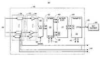
- FIG. 4is a functional block diagram of an optical channel analyzing switch in accordance with a preferred embodiment of the present invention.
- An analyzing system 400is depicted as including an optical channel analyzing switch 402 for selecting a specific channel from among a plurality of channels 404 for coupling with test equipment 406 .
- Plurality of channels 404is comprised of optical channels which may be implemented as single-mode or multi-mode fibers and operated at various channel standards and capacities such as Gigabit Ethernet or Fibre Channel.
- the present inventionfacilitates the monitoring and evaluation of a specific channel without interruption to that specific channel's traffic.
- Such an implementationis facilitated by coupling channels 404 to individual optical couplers 408 which split or “tap” each of the individual channels and provide two groups of outputs, one being a group of pass-through outputs 410 and a second group of outputs depicted as analyzable output optical signals 412 .
- cascading capabilities of this embodimentis that two or more units and associated switches can be combined to tap and analyze more channels than could be handled by a single unit.
- the combined, or cascaded, switchescan be controlled together as a single combined system.
- Analyzable output optical signals 412directly couple with receivers 414 which perform optical-to-electrical conversion thereby facilitating the signal timing and manipulation in electrical form as opposed to the more complex optical signal manipulation.
- Receivers 414convert analyzable output optical signals 414 into analyzable electrical signals 416 which are coupled to a multiplexor 418 , which in FIG. 4 is depicted for illustrative purposes only as being an 8-to-1 multiplexor.
- Multiplexor 418selects, according to control signal 420 , one of the input signals from among analyzable electrical signals 416 as the output signal depicted as multiplexor output signal 422 .
- Signal 422then undergoes various signal modifications in order to restore the timing relationship of the signal which has been contaminated by the extended propagation path through optical channel analyzing switch 402 as well as the noise contamination inherent in electrical devices and components within optical channel analyzing switch 402 .
- a retimer 424receives a multiplexor output signal 422 in electrical form and performs a clock recovery function which extracts the clock from the serial data and generates retimed data signal. This retiming operation reduces the jitter that would otherwise be introduced into the signal provided to the test equipment 406 . In this manner, the optical channel analyzing switches of the invention provide significant advantages over switches of the prior art.
- a transmitter 436receives retimed electrical analyzable output signals 434 in electrical form and transforms those electrical signals into a retimed optical analyzable output signal 438 which is an approximation in optical form of the selected input signal from among the plurality of channels 404 selected by multiplexor 418 .
- optical channel analyzing switch 402performs transducing operations to process the output signal 438 such that it complies with the input signal requirements of the test equipment.
- optical channel analyzing switch 402includes a transmitter 436 that is selected to process the output signal 438 in an appropriate manner such that the output signal complies with the input signal requirements of the test equipment.
- the type of transmitter 436is typically determined by the type of test equipment (optical or electrical) with which the optical channel analyzing switch is to be used.
- the present inventionalso includes an embodiment capable of cascading or coupling a plurality of optical channel analyzer switches, such as 402 , for selecting from among an even greater plurality of inputs 404 .
- Transmitter 436includes electrical outputs 440 , which may be further coupled with a multiplexor of another optical channel analyzer switch as depicted in FIG. 3 .
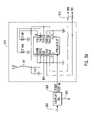
- FIGS. 5A–5Drepresent a schematic diagram of a single channel of the optical channel analyzing switch, in accordance with one implementation of the preferred embodiment of the present invention.
- input optical signal 502is coupled to a multi-mode wide-band fiber coupler 504 .
- coupler 504is further comprised of two output signals, a pass-through output signal 506 and an analyzable output optical signal 508 in optical form. It is desirable that coupler 504 exhibit low insertion loss, high directivity, high stability and reliability and low excess loss.
- coupler 504may be comprised of a multi-mode coupler such as an MMC-Multimode Wideband Fiber Coupler, manufactured by Transwave Fiber, Inc., of Fremont, Calif.
- Optical signal 508is coupled to a receiver portion which exhibits acceptable operational characteristics in converting from optical to electrical transmissions. It would be desirable for a receiver 510 to exhibit high-speed data rates up to and in excess of 2.125 Gbit/sec which is compatible with Fibre Channel and Gigabit Ethernet data rates. Additionally, receiver 510 would desirably exhibit very low jitter, low power dissipation, and for ease of integration exhibit a small form-factor. By way of example and not limitation, receiver 510 may be comprised of transceiver implemented in a receiver mode only such as a 2 gigabit/2 ⁇ 5 transceiver FTRJ-8519-1-25 available from Finisar Systems of Sunnyvale, Calif.
- a receiver 510generates analyzable electrical signals 512 , now in electronic rather than optical form which are coupled to a multiplexor 514 . It is desirable that multiplexor 514 exhibit sufficient addressability for individually selecting from among the plurality of possible channels presented to the optical channel analyzing switch 500 . Also, multiplexor 514 desirably operates at propagation delays and frequencies consistent with the frequencies of the communication standards being evaluated.
- FIGS. 5A–5Dillustrate multiplexor 514 implemented using a plurality of discrete 4-to-1 multiplexors arranged to implement an 8-to-1 multiplexor configuration.
- multiplexor 514is implemented using a plurality of multiplexor devices such as the MC10EP57 and MC10EL57 available from ON Semiconductor, Phoenix, Ariz.
- the selected output signals 516 including reference clock signals 520are coupled to a retimer circuit 518 to generate output data signals 522 and output clock signals 524 .
- Retimer 518extracts the clock from the serial data and generates retimed clock signal 524 and retimed data signal 522 .
- Retimer circuit 518desirably performs continuous-rate clock and data recovery, at the desirable data rate standards of at least Fibre Channel and Gigabit Ethernet. It is also desirable for retimer circuit 518 to exhibit low jitter and sufficient input sensitivity.
- retimer circuit 518may be comprised of an S3056 clock recovery device that performs the clock recovery function for various optical standards including SONET, Fibre Channel, and Gigabit, Ethernet.
- the S3056is capable of operating at 30 Mbps to 2.7 Gbps continuous-rate clock and data recovery.
- the exemplary deviceis available from Applied Micro Circuits Corporation of San Diego, Calif.
- Output signals 522 and 524are further coupled to a latch or flip-flop configuration 526 .
- the purpose of latch 526is to recombine the timing-realigned separated clock signal 524 and data signal 522 into combined retimed electrical analyzable output signal 528 .
- an exemplary latch configuration 526may be comprised of a “D” flip-flop such as an MC100EP52 available from various sources including ON Semiconductor, Phoenix, Ariz.
- Outputs 528are further coupled to a transmitter for converting from an electrical signal to an optical signal by way of a transmitter 530 .
- Transmitter 530generates an optical output 532 for coupling with the test equipment.
- Transmitter 530also alternatively generates cascading signals 534 for coupling with additional switches in an alternate embodiment, as discussed above.
- an exemplary transmitter 530may be comprised of a FTRJ-8519-1-25 available from Finisar Systems of San Jose, Calif.
Landscapes
- Physics & Mathematics (AREA)
- Electromagnetism (AREA)
- Engineering & Computer Science (AREA)
- Computer Networks & Wireless Communication (AREA)
- Signal Processing (AREA)
- Optical Communication System (AREA)
Abstract
Description
Claims (21)
Priority Applications (1)
| Application Number | Priority Date | Filing Date | Title |
|---|---|---|---|
| US09/971,970US7031615B2 (en) | 2001-10-04 | 2001-10-04 | Optical channel selection and evaluation system |
Applications Claiming Priority (1)
| Application Number | Priority Date | Filing Date | Title |
|---|---|---|---|
| US09/971,970US7031615B2 (en) | 2001-10-04 | 2001-10-04 | Optical channel selection and evaluation system |
Publications (2)
| Publication Number | Publication Date |
|---|---|
| US20030067656A1 US20030067656A1 (en) | 2003-04-10 |
| US7031615B2true US7031615B2 (en) | 2006-04-18 |
Family
ID=29216385
Family Applications (1)
| Application Number | Title | Priority Date | Filing Date |
|---|---|---|---|
| US09/971,970Expired - LifetimeUS7031615B2 (en) | 2001-10-04 | 2001-10-04 | Optical channel selection and evaluation system |
Country Status (1)
| Country | Link |
|---|---|
| US (1) | US7031615B2 (en) |
Cited By (37)
| Publication number | Priority date | Publication date | Assignee | Title |
|---|---|---|---|---|
| US20040071389A1 (en)* | 2002-09-13 | 2004-04-15 | Hofmeister Rudolf J. | Optical and electrical channel feedback in optical transceiver module |
| US20040076113A1 (en)* | 2002-06-25 | 2004-04-22 | Aronson Lewis B. | Transceiver module and integrated circuit with multi-rate eye openers and bypass |
| US20050015518A1 (en)* | 2003-07-16 | 2005-01-20 | Wen William J. | Method and system for non-disruptive data capture in networks |
| US20050018674A1 (en)* | 2003-07-21 | 2005-01-27 | Dropps Frank R. | Method and system for buffer-to-buffer credit recovery in fibre channel systems using virtual and/or pseudo virtual lanes |
| US20050018680A1 (en)* | 2003-07-21 | 2005-01-27 | Dropps Frank R. | Method and system for programmable data dependant network routing |
| US20050018649A1 (en)* | 2003-07-21 | 2005-01-27 | Dropps Frank R. | Method and system for improving bandwidth and reducing idles in fibre channel switches |
| US20050018650A1 (en)* | 2003-07-21 | 2005-01-27 | Dropps Frank R. | Method and system for configuring fibre channel ports |
| US20050030893A1 (en)* | 2003-07-21 | 2005-02-10 | Dropps Frank R. | Method and system for detecting congestion and over subscription in a fibre channel network |
| US20050030954A1 (en)* | 2003-07-21 | 2005-02-10 | Dropps Frank R. | Method and system for programmable data dependant network routing |
| US20050111845A1 (en)* | 2002-06-25 | 2005-05-26 | Stephen Nelson | Apparatus, system and methods for modifying operating characteristics of optoelectronic devices |
| US20050135251A1 (en)* | 2002-10-07 | 2005-06-23 | Kunz James A. | Method and system for reducing congestion in computer networks |
| US20050174942A1 (en)* | 2004-02-05 | 2005-08-11 | Betker Steven M. | Method and system for reducing deadlock in fibre channel fabrics using virtual lanes |
| US20060072473A1 (en)* | 2004-10-01 | 2006-04-06 | Dropps Frank R | High speed fibre channel switch element |
| US20060072616A1 (en)* | 2004-10-01 | 2006-04-06 | Dropps Frank R | Method and system for LUN remapping in fibre channel networks |
| US20070229040A1 (en)* | 2006-03-30 | 2007-10-04 | Eudyna Devices Inc. | Electronic device, method for controlling the same, and optical semiconductor module |
| US20080181615A1 (en)* | 2007-01-26 | 2008-07-31 | Bti Photonic Systems Inc. | Method and system for dynamic dispersion compensation |
| US20080219249A1 (en)* | 2004-04-23 | 2008-09-11 | Mcglaughlin Edward C | Fibre channel transparent switch for mixed switch fabrics |
| US7437079B1 (en) | 2002-06-25 | 2008-10-14 | Finisar Corporation | Automatic selection of data rate for optoelectronic devices |
| US20080310306A1 (en)* | 2003-07-21 | 2008-12-18 | Dropps Frank R | Programmable pseudo virtual lanes for fibre channel systems |
| US20090034550A1 (en)* | 2003-07-21 | 2009-02-05 | Dropps Frank R | Method and system for routing fibre channel frames |
| US20090041029A1 (en)* | 2003-07-21 | 2009-02-12 | Dropps Frank R | Method and system for managing traffic in fibre channel systems |
| US20090046736A1 (en)* | 2004-07-20 | 2009-02-19 | Dropps Frank R | Method and system for keeping a fibre channel arbitrated loop open during frame gaps |
| US7519058B2 (en) | 2005-01-18 | 2009-04-14 | Qlogic, Corporation | Address translation in fibre channel switches |
| US7525983B2 (en) | 2003-07-21 | 2009-04-28 | Qlogic, Corporation | Method and system for selecting virtual lanes in fibre channel switches |
| US7561855B2 (en) | 2002-06-25 | 2009-07-14 | Finisar Corporation | Transceiver module and integrated circuit with clock and data recovery clock diplexing |
| US7580354B2 (en) | 2003-07-21 | 2009-08-25 | Qlogic, Corporation | Multi-speed cut through operation in fibre channel switches |
| US7620059B2 (en) | 2003-07-16 | 2009-11-17 | Qlogic, Corporation | Method and apparatus for accelerating receive-modify-send frames in a fibre channel network |
| US7684401B2 (en) | 2003-07-21 | 2010-03-23 | Qlogic, Corporation | Method and system for using extended fabric features with fibre channel switch elements |
| US7729288B1 (en) | 2002-09-11 | 2010-06-01 | Qlogic, Corporation | Zone management in a multi-module fibre channel switch |
| US7792115B2 (en) | 2003-07-21 | 2010-09-07 | Qlogic, Corporation | Method and system for routing and filtering network data packets in fibre channel systems |
| US7809275B2 (en) | 2002-06-25 | 2010-10-05 | Finisar Corporation | XFP transceiver with 8.5G CDR bypass |
| US7822061B2 (en) | 2003-07-21 | 2010-10-26 | Qlogic, Corporation | Method and system for power control of fibre channel switches |
| US7894348B2 (en) | 2003-07-21 | 2011-02-22 | Qlogic, Corporation | Method and system for congestion control in a fibre channel switch |
| US7930377B2 (en) | 2004-04-23 | 2011-04-19 | Qlogic, Corporation | Method and system for using boot servers in networks |
| US20160315701A1 (en)* | 2015-04-24 | 2016-10-27 | Fujitsu Limited | Optical transmission device, method for verifying connection, and wavelength selective switch card |
| US10886927B2 (en) | 2019-01-15 | 2021-01-05 | SK Hynix Inc. | Signal generation circuit synchronized with a clock signal and a semiconductor apparatus using the same |
| US11126216B2 (en) | 2019-01-15 | 2021-09-21 | SK Hynix Inc. | Signal generation circuit synchronized with a clock signal and a semiconductor apparatus using the same |
Families Citing this family (6)
| Publication number | Priority date | Publication date | Assignee | Title |
|---|---|---|---|---|
| KR100687723B1 (en)* | 2004-12-17 | 2007-02-27 | 한국전자통신연구원 | Operation test device of optical transceiver |
| US7945164B2 (en)* | 2006-05-25 | 2011-05-17 | Cisco Technology, Inc. | Multiple fiber optic gigabit ethernet links channelized over single optical link |
| US8438425B1 (en)* | 2007-12-26 | 2013-05-07 | Emc (Benelux) B.V., S.A.R.L. | Testing a device for use in a storage area network |
| US9319148B2 (en)* | 2012-10-01 | 2016-04-19 | Lenovo Enterprise Solutions (Singapore) Pte. Ltd. | Optical interconnection to an integrated circuit |
| US9104654B2 (en)* | 2013-09-09 | 2015-08-11 | Sandisk Technologies Inc. | Method and device for efficient trace analysis |
| JP2022132859A (en)* | 2021-03-01 | 2022-09-13 | 富士通株式会社 | Optical transmission device and optical transmission system |
Citations (13)
| Publication number | Priority date | Publication date | Assignee | Title |
|---|---|---|---|---|
| US5080506A (en) | 1988-05-20 | 1992-01-14 | Raynet Corp. | Optical fiber tap for monitoring laser input power |
| US5406260A (en) | 1992-12-18 | 1995-04-11 | Chrimar Systems, Inc. | Network security system for detecting removal of electronic equipment |
| US5491402A (en) | 1993-07-20 | 1996-02-13 | Echelon Corporation | Apparatus and method for providing AC isolation while supplying DC power |
| US5721796A (en) | 1996-06-21 | 1998-02-24 | Lucent Technologies Inc. | Optical fiber cross connect with active routing for wavelength multiplexing and demultiplexing |
| US5878030A (en) | 1996-06-19 | 1999-03-02 | Wandel & Goltermann Technologies, Inc. | Test access port for analyzing high-speed local area network switched environment |
| US6115468A (en) | 1998-03-26 | 2000-09-05 | Cisco Technology, Inc. | Power feed for Ethernet telephones via Ethernet link |
| US6141763A (en) | 1998-09-01 | 2000-10-31 | Hewlett-Packard Company | Self-powered network access point |
| US6140911A (en) | 1997-05-29 | 2000-10-31 | 3Com Corporation | Power transfer apparatus for concurrently transmitting data and power over data wires |
| US6218930B1 (en) | 1999-03-10 | 2001-04-17 | Merlot Communications | Apparatus and method for remotely powering access equipment over a 10/100 switched ethernet network |
| US6236478B1 (en)* | 1998-06-23 | 2001-05-22 | Siemens Aktiengesellschaft | Method for monitoring optical communication equipment |
| US6246497B1 (en) | 1998-03-12 | 2001-06-12 | Net-Hopper Systems, Inc. | Active optical loop-back system |
| US6522436B2 (en)* | 1998-02-11 | 2003-02-18 | Nortel Networks Limited | Multiplexed transmission of optical signals |
| US6810215B1 (en)* | 1999-07-15 | 2004-10-26 | Fujitsu Limited | Optical repeater converting wavelength and bit rate between networks |
- 2001
- 2001-10-04USUS09/971,970patent/US7031615B2/ennot_activeExpired - Lifetime
Patent Citations (13)
| Publication number | Priority date | Publication date | Assignee | Title |
|---|---|---|---|---|
| US5080506A (en) | 1988-05-20 | 1992-01-14 | Raynet Corp. | Optical fiber tap for monitoring laser input power |
| US5406260A (en) | 1992-12-18 | 1995-04-11 | Chrimar Systems, Inc. | Network security system for detecting removal of electronic equipment |
| US5491402A (en) | 1993-07-20 | 1996-02-13 | Echelon Corporation | Apparatus and method for providing AC isolation while supplying DC power |
| US5878030A (en) | 1996-06-19 | 1999-03-02 | Wandel & Goltermann Technologies, Inc. | Test access port for analyzing high-speed local area network switched environment |
| US5721796A (en) | 1996-06-21 | 1998-02-24 | Lucent Technologies Inc. | Optical fiber cross connect with active routing for wavelength multiplexing and demultiplexing |
| US6140911A (en) | 1997-05-29 | 2000-10-31 | 3Com Corporation | Power transfer apparatus for concurrently transmitting data and power over data wires |
| US6522436B2 (en)* | 1998-02-11 | 2003-02-18 | Nortel Networks Limited | Multiplexed transmission of optical signals |
| US6246497B1 (en) | 1998-03-12 | 2001-06-12 | Net-Hopper Systems, Inc. | Active optical loop-back system |
| US6115468A (en) | 1998-03-26 | 2000-09-05 | Cisco Technology, Inc. | Power feed for Ethernet telephones via Ethernet link |
| US6236478B1 (en)* | 1998-06-23 | 2001-05-22 | Siemens Aktiengesellschaft | Method for monitoring optical communication equipment |
| US6141763A (en) | 1998-09-01 | 2000-10-31 | Hewlett-Packard Company | Self-powered network access point |
| US6218930B1 (en) | 1999-03-10 | 2001-04-17 | Merlot Communications | Apparatus and method for remotely powering access equipment over a 10/100 switched ethernet network |
| US6810215B1 (en)* | 1999-07-15 | 2004-10-26 | Fujitsu Limited | Optical repeater converting wavelength and bit rate between networks |
Cited By (64)
| Publication number | Priority date | Publication date | Assignee | Title |
|---|---|---|---|---|
| US7664401B2 (en) | 2002-06-25 | 2010-02-16 | Finisar Corporation | Apparatus, system and methods for modifying operating characteristics of optoelectronic devices |
| US20050111845A1 (en)* | 2002-06-25 | 2005-05-26 | Stephen Nelson | Apparatus, system and methods for modifying operating characteristics of optoelectronic devices |
| US20040076119A1 (en)* | 2002-06-25 | 2004-04-22 | Aronson Lewis B. | Transceiver module and integrated circuit with dual eye openers and integrated loopback and bit error rate testing |
| US20040091028A1 (en)* | 2002-06-25 | 2004-05-13 | Aronson Lewis B. | Transceiver module and integrated circuit with dual eye openers and equalizer |
| US7486894B2 (en) | 2002-06-25 | 2009-02-03 | Finisar Corporation | Transceiver module and integrated circuit with dual eye openers |
| US7995927B2 (en) | 2002-06-25 | 2011-08-09 | Finisar Corporation | Transceiver module and integrated circuit with dual eye openers |
| US7835648B2 (en) | 2002-06-25 | 2010-11-16 | Finisar Corporation | Automatic selection of data rate for optoelectronic devices |
| US7809275B2 (en) | 2002-06-25 | 2010-10-05 | Finisar Corporation | XFP transceiver with 8.5G CDR bypass |
| US7437079B1 (en) | 2002-06-25 | 2008-10-14 | Finisar Corporation | Automatic selection of data rate for optoelectronic devices |
| US20100111539A1 (en)* | 2002-06-25 | 2010-05-06 | Finisar Corporation | Transceiver module and integrated circuit with dual eye openers |
| US20040076113A1 (en)* | 2002-06-25 | 2004-04-22 | Aronson Lewis B. | Transceiver module and integrated circuit with multi-rate eye openers and bypass |
| US7561855B2 (en) | 2002-06-25 | 2009-07-14 | Finisar Corporation | Transceiver module and integrated circuit with clock and data recovery clock diplexing |
| US7567758B2 (en)* | 2002-06-25 | 2009-07-28 | Finisar Corporation | Transceiver module and integrated circuit with multi-rate eye openers and bypass |
| US7613393B2 (en) | 2002-06-25 | 2009-11-03 | Finisar Corporation | Transceiver module and integrated circuit with dual eye openers and integrated loopback and bit error rate testing |
| US7729288B1 (en) | 2002-09-11 | 2010-06-01 | Qlogic, Corporation | Zone management in a multi-module fibre channel switch |
| US7477847B2 (en) | 2002-09-13 | 2009-01-13 | Finisar Corporation | Optical and electrical channel feedback in optical transceiver module |
| US20040071389A1 (en)* | 2002-09-13 | 2004-04-15 | Hofmeister Rudolf J. | Optical and electrical channel feedback in optical transceiver module |
| US20050135251A1 (en)* | 2002-10-07 | 2005-06-23 | Kunz James A. | Method and system for reducing congestion in computer networks |
| US7620059B2 (en) | 2003-07-16 | 2009-11-17 | Qlogic, Corporation | Method and apparatus for accelerating receive-modify-send frames in a fibre channel network |
| US7525910B2 (en) | 2003-07-16 | 2009-04-28 | Qlogic, Corporation | Method and system for non-disruptive data capture in networks |
| US20050015518A1 (en)* | 2003-07-16 | 2005-01-20 | Wen William J. | Method and system for non-disruptive data capture in networks |
| US7558281B2 (en)* | 2003-07-21 | 2009-07-07 | Qlogic, Corporation | Method and system for configuring fibre channel ports |
| US20050018649A1 (en)* | 2003-07-21 | 2005-01-27 | Dropps Frank R. | Method and system for improving bandwidth and reducing idles in fibre channel switches |
| US20090034550A1 (en)* | 2003-07-21 | 2009-02-05 | Dropps Frank R | Method and system for routing fibre channel frames |
| US20090041029A1 (en)* | 2003-07-21 | 2009-02-12 | Dropps Frank R | Method and system for managing traffic in fibre channel systems |
| US20050018674A1 (en)* | 2003-07-21 | 2005-01-27 | Dropps Frank R. | Method and system for buffer-to-buffer credit recovery in fibre channel systems using virtual and/or pseudo virtual lanes |
| US7936771B2 (en) | 2003-07-21 | 2011-05-03 | Qlogic, Corporation | Method and system for routing fibre channel frames |
| US7522529B2 (en) | 2003-07-21 | 2009-04-21 | Qlogic, Corporation | Method and system for detecting congestion and over subscription in a fibre channel network |
| US7525983B2 (en) | 2003-07-21 | 2009-04-28 | Qlogic, Corporation | Method and system for selecting virtual lanes in fibre channel switches |
| US7894348B2 (en) | 2003-07-21 | 2011-02-22 | Qlogic, Corporation | Method and system for congestion control in a fibre channel switch |
| US20050018680A1 (en)* | 2003-07-21 | 2005-01-27 | Dropps Frank R. | Method and system for programmable data dependant network routing |
| US7822061B2 (en) | 2003-07-21 | 2010-10-26 | Qlogic, Corporation | Method and system for power control of fibre channel switches |
| US20080310306A1 (en)* | 2003-07-21 | 2008-12-18 | Dropps Frank R | Programmable pseudo virtual lanes for fibre channel systems |
| US7792115B2 (en) | 2003-07-21 | 2010-09-07 | Qlogic, Corporation | Method and system for routing and filtering network data packets in fibre channel systems |
| US7760752B2 (en) | 2003-07-21 | 2010-07-20 | Qlogic, Corporation | Programmable pseudo virtual lanes for fibre channel systems |
| US7573909B2 (en) | 2003-07-21 | 2009-08-11 | Qlogic, Corporation | Method and system for programmable data dependant network routing |
| US7580354B2 (en) | 2003-07-21 | 2009-08-25 | Qlogic, Corporation | Multi-speed cut through operation in fibre channel switches |
| US7583597B2 (en) | 2003-07-21 | 2009-09-01 | Qlogic Corporation | Method and system for improving bandwidth and reducing idles in fibre channel switches |
| US20050018650A1 (en)* | 2003-07-21 | 2005-01-27 | Dropps Frank R. | Method and system for configuring fibre channel ports |
| US20050030893A1 (en)* | 2003-07-21 | 2005-02-10 | Dropps Frank R. | Method and system for detecting congestion and over subscription in a fibre channel network |
| US7684401B2 (en) | 2003-07-21 | 2010-03-23 | Qlogic, Corporation | Method and system for using extended fabric features with fibre channel switch elements |
| US7630384B2 (en) | 2003-07-21 | 2009-12-08 | Qlogic, Corporation | Method and system for distributing credit in fibre channel systems |
| US7646767B2 (en) | 2003-07-21 | 2010-01-12 | Qlogic, Corporation | Method and system for programmable data dependant network routing |
| US7649903B2 (en) | 2003-07-21 | 2010-01-19 | Qlogic, Corporation | Method and system for managing traffic in fibre channel systems |
| US20050030954A1 (en)* | 2003-07-21 | 2005-02-10 | Dropps Frank R. | Method and system for programmable data dependant network routing |
| US20050174942A1 (en)* | 2004-02-05 | 2005-08-11 | Betker Steven M. | Method and system for reducing deadlock in fibre channel fabrics using virtual lanes |
| US7564789B2 (en) | 2004-02-05 | 2009-07-21 | Qlogic, Corporation | Method and system for reducing deadlock in fibre channel fabrics using virtual lanes |
| US7930377B2 (en) | 2004-04-23 | 2011-04-19 | Qlogic, Corporation | Method and system for using boot servers in networks |
| US20080219249A1 (en)* | 2004-04-23 | 2008-09-11 | Mcglaughlin Edward C | Fibre channel transparent switch for mixed switch fabrics |
| US7542676B2 (en) | 2004-04-23 | 2009-06-02 | Qlogic, Corporation | Fibre channel transparent switch for mixed switch fabrics |
| US7822057B2 (en) | 2004-07-20 | 2010-10-26 | Qlogic, Corporation | Method and system for keeping a fibre channel arbitrated loop open during frame gaps |
| US20090046736A1 (en)* | 2004-07-20 | 2009-02-19 | Dropps Frank R | Method and system for keeping a fibre channel arbitrated loop open during frame gaps |
| US20060072616A1 (en)* | 2004-10-01 | 2006-04-06 | Dropps Frank R | Method and system for LUN remapping in fibre channel networks |
| US7593997B2 (en) | 2004-10-01 | 2009-09-22 | Qlogic, Corporation | Method and system for LUN remapping in fibre channel networks |
| US20060072473A1 (en)* | 2004-10-01 | 2006-04-06 | Dropps Frank R | High speed fibre channel switch element |
| US8295299B2 (en) | 2004-10-01 | 2012-10-23 | Qlogic, Corporation | High speed fibre channel switch element |
| US7519058B2 (en) | 2005-01-18 | 2009-04-14 | Qlogic, Corporation | Address translation in fibre channel switches |
| US20070229040A1 (en)* | 2006-03-30 | 2007-10-04 | Eudyna Devices Inc. | Electronic device, method for controlling the same, and optical semiconductor module |
| US7710083B2 (en)* | 2006-03-30 | 2010-05-04 | Eudyna Devices Inc. | Electronic device, method for controlling the same, and optical semiconductor module |
| US20080181615A1 (en)* | 2007-01-26 | 2008-07-31 | Bti Photonic Systems Inc. | Method and system for dynamic dispersion compensation |
| US7796895B2 (en)* | 2007-01-26 | 2010-09-14 | Bti Systems Inc. | Method and system for dynamic dispersion compensation |
| US20160315701A1 (en)* | 2015-04-24 | 2016-10-27 | Fujitsu Limited | Optical transmission device, method for verifying connection, and wavelength selective switch card |
| US10886927B2 (en) | 2019-01-15 | 2021-01-05 | SK Hynix Inc. | Signal generation circuit synchronized with a clock signal and a semiconductor apparatus using the same |
| US11126216B2 (en) | 2019-01-15 | 2021-09-21 | SK Hynix Inc. | Signal generation circuit synchronized with a clock signal and a semiconductor apparatus using the same |
Also Published As
| Publication number | Publication date |
|---|---|
| US20030067656A1 (en) | 2003-04-10 |
Similar Documents
| Publication | Publication Date | Title |
|---|---|---|
| US7031615B2 (en) | Optical channel selection and evaluation system | |
| EP1171967B1 (en) | Method and monitoring device for monitoring the quality of data transmission over analog lines | |
| US6785242B2 (en) | Apparatus and method to monitor communication system status | |
| US6990294B2 (en) | Optical network system with quality control function | |
| US8270845B2 (en) | Multimode fiber tap for a LRM connection | |
| US6950972B2 (en) | Multi-purpose BER tester (MPBERT) for very high RZ and NRZ signals | |
| US20020021468A1 (en) | Semiconductor integrated circuit having receiving and transmitting units formed on a single semiconductor chip with a test signal input port | |
| JP2020048177A (en) | Apparatus and method for matching optical fiber connection on ROADM service side | |
| US7218861B2 (en) | Optical transceiver, a multiplexing integrated circuit, a demultiplexing integrated circuit, an integral multiplexing/demultiplexing integrated circuit, and method for evaluating and testing the optical transceiver | |
| GB2419055A (en) | Optical and electrical channel feedback in optical transceiver module | |
| US6208621B1 (en) | Apparatus and method for testing the ability of a pair of serial data transceivers to transmit serial data at one frequency and to receive serial data at another frequency | |
| JP2000142599A (en) | Connector interface for spacecraft modules | |
| US8285154B2 (en) | System and method for multi-rate, high-sensitivity clock and data recovery with adjustable decision threshold, RF input, and optical-to-electrical conversion | |
| US20070280591A1 (en) | Optical network test access point device | |
| JP2002107419A (en) | Semiconductor integrated circuit | |
| CN100459478C (en) | Multi-channel optical wavelength locking device and method in optical communication system | |
| CA1130409A (en) | Half-duplex/simplex digital signal converter | |
| US7639655B2 (en) | Ethernet switch interface for use in optical nodes | |
| US7394980B1 (en) | Systems and methods for testing a circuit in a communication network | |
| US20080005376A1 (en) | Apparatus for a non-intrusive ieee1394b-2002 bus interface including data monitoring functions of critical physical layer stages | |
| US20060188259A1 (en) | HDSL optical fiber transmission system and method | |
| US20060010336A1 (en) | Connection apparatus and method for network testers and analysers | |
| US6847787B2 (en) | WDM network node module | |
| AU2001294521B2 (en) | Fiber protection and non-intrusive expansion methods and apparatus | |
| US6570693B2 (en) | Reverse path optical combining using an optical commutator |
Legal Events
| Date | Code | Title | Description |
|---|---|---|---|
| AS | Assignment | Owner name:FINISAR CORPORATION, CALIFORNIA Free format text:ASSIGNMENT OF ASSIGNORS INTEREST;ASSIGNOR:GENTILE, PHILIP J.;REEL/FRAME:012239/0147 Effective date:20010924 | |
| STCF | Information on status: patent grant | Free format text:PATENTED CASE | |
| FPAY | Fee payment | Year of fee payment:4 | |
| AS | Assignment | Owner name:JDS UNIPHASE CORPORATION, CALIFORNIA Free format text:ASSIGNMENT OF ASSIGNORS INTEREST;ASSIGNOR:FINISAR CORPORATION;REEL/FRAME:025730/0518 Effective date:20090713 | |
| CC | Certificate of correction | ||
| FPAY | Fee payment | Year of fee payment:8 | |
| AS | Assignment | Owner name:VIAVI SOLUTIONS INC., CALIFORNIA Free format text:CHANGE OF NAME;ASSIGNOR:JDS UNIPHASE CORPORATION;REEL/FRAME:037057/0627 Effective date:20150731 | |
| FEPP | Fee payment procedure | Free format text:PAYER NUMBER DE-ASSIGNED (ORIGINAL EVENT CODE: RMPN); ENTITY STATUS OF PATENT OWNER: LARGE ENTITY Free format text:PAYOR NUMBER ASSIGNED (ORIGINAL EVENT CODE: ASPN); ENTITY STATUS OF PATENT OWNER: LARGE ENTITY | |
| MAFP | Maintenance fee payment | Free format text:PAYMENT OF MAINTENANCE FEE, 12TH YEAR, LARGE ENTITY (ORIGINAL EVENT CODE: M1553) Year of fee payment:12 | |
| AS | Assignment | Owner name:WELLS FARGO BANK, NATIONAL ASSOCIATION, AS ADMINISTRATIVE AGENT, COLORADO Free format text:SECURITY INTEREST;ASSIGNORS:VIAVI SOLUTIONS INC.;3Z TELECOM, INC.;ACTERNA LLC;AND OTHERS;REEL/FRAME:052729/0321 Effective date:20200519 | |
| AS | Assignment | Owner name:RPC PHOTONICS, INC., NEW YORK Free format text:TERMINATIONS OF SECURITY INTEREST AT REEL 052729, FRAME 0321;ASSIGNOR:WELLS FARGO BANK, NATIONAL ASSOCIATION, AS ADMINISTRATIVE AGENT;REEL/FRAME:058666/0639 Effective date:20211229 Owner name:VIAVI SOLUTIONS INC., CALIFORNIA Free format text:TERMINATIONS OF SECURITY INTEREST AT REEL 052729, FRAME 0321;ASSIGNOR:WELLS FARGO BANK, NATIONAL ASSOCIATION, AS ADMINISTRATIVE AGENT;REEL/FRAME:058666/0639 Effective date:20211229 |