US7029996B2 - Methods for producing uniform large-grained and grain boundary location manipulated polycrystalline thin film semiconductors using sequential lateral solidification - Google Patents
Methods for producing uniform large-grained and grain boundary location manipulated polycrystalline thin film semiconductors using sequential lateral solidificationDownload PDFInfo
- Publication number
- US7029996B2 US7029996B2US10/294,001US29400102AUS7029996B2US 7029996 B2US7029996 B2US 7029996B2US 29400102 AUS29400102 AUS 29400102AUS 7029996 B2US7029996 B2US 7029996B2
- Authority
- US
- United States
- Prior art keywords
- sample
- thin film
- sequence
- silicon
- silicon thin
- Prior art date
- Legal status (The legal status is an assumption and is not a legal conclusion. Google has not performed a legal analysis and makes no representation as to the accuracy of the status listed.)
- Expired - Fee Related, expires
Links
- 238000000034methodMethods0.000titleclaimsabstractdescription55
- 239000010409thin filmSubstances0.000titleabstractdescription38
- 239000004065semiconductorSubstances0.000titledescription12
- 238000007711solidificationMethods0.000titledescription11
- 230000008023solidificationEffects0.000titledescription11
- XUIMIQQOPSSXEZ-UHFFFAOYSA-NSiliconChemical compound[Si]XUIMIQQOPSSXEZ-UHFFFAOYSA-N0.000claimsabstractdescription53
- 229910052710siliconInorganic materials0.000claimsabstractdescription52
- 239000010703siliconSubstances0.000claimsabstractdescription52
- 229910021417amorphous siliconInorganic materials0.000claimsabstractdescription23
- 230000008018meltingEffects0.000claimsabstractdescription6
- 238000002844meltingMethods0.000claimsabstractdescription6
- 239000000758substrateSubstances0.000claimsdescription3
- 238000000137annealingMethods0.000claims8
- 229910021420polycrystalline siliconInorganic materials0.000abstractdescription29
- 230000008569processEffects0.000abstractdescription27
- 230000000873masking effectEffects0.000abstractdescription25
- 238000012545processingMethods0.000abstractdescription10
- 230000006911nucleationEffects0.000abstractdescription5
- 238000010899nucleationMethods0.000abstractdescription5
- 230000000694effectsEffects0.000abstractdescription4
- 230000001678irradiating effectEffects0.000abstractdescription4
- 239000013078crystalSubstances0.000description34
- 238000010586diagramMethods0.000description22
- 238000013519translationMethods0.000description21
- 239000010408filmSubstances0.000description19
- 238000004519manufacturing processMethods0.000description6
- 230000015572biosynthetic processEffects0.000description3
- 238000002425crystallisationMethods0.000description3
- 230000008025crystallizationEffects0.000description3
- 239000010432diamondSubstances0.000description3
- 229910003460diamondInorganic materials0.000description3
- 239000000155meltSubstances0.000description3
- 241000280258Dyschoriste linearisSpecies0.000description2
- 230000009286beneficial effectEffects0.000description2
- 238000000265homogenisationMethods0.000description2
- 238000005224laser annealingMethods0.000description2
- 238000000926separation methodMethods0.000description2
- 230000004075alterationEffects0.000description1
- 230000008859changeEffects0.000description1
- 239000011248coating agentSubstances0.000description1
- 238000000576coating methodMethods0.000description1
- 238000004320controlled atmosphereMethods0.000description1
- 238000007796conventional methodMethods0.000description1
- 229910021419crystalline siliconInorganic materials0.000description1
- 230000007123defenseEffects0.000description1
- 239000010438graniteSubstances0.000description1
- 239000004973liquid crystal related substanceSubstances0.000description1
- 239000011159matrix materialSubstances0.000description1
- 238000012986modificationMethods0.000description1
- 230000004048modificationEffects0.000description1
- 229910021421monocrystalline siliconInorganic materials0.000description1
- 230000003287optical effectEffects0.000description1
- 229920005591polysiliconPolymers0.000description1
- 239000010453quartzSubstances0.000description1
- 230000009467reductionEffects0.000description1
- 238000011160researchMethods0.000description1
- VYPSYNLAJGMNEJ-UHFFFAOYSA-Nsilicon dioxideInorganic materialsO=[Si]=OVYPSYNLAJGMNEJ-UHFFFAOYSA-N0.000description1
Images


Classifications
- B—PERFORMING OPERATIONS; TRANSPORTING
- B23—MACHINE TOOLS; METAL-WORKING NOT OTHERWISE PROVIDED FOR
- B23K—SOLDERING OR UNSOLDERING; WELDING; CLADDING OR PLATING BY SOLDERING OR WELDING; CUTTING BY APPLYING HEAT LOCALLY, e.g. FLAME CUTTING; WORKING BY LASER BEAM
- B23K26/00—Working by laser beam, e.g. welding, cutting or boring
- B23K26/02—Positioning or observing the workpiece, e.g. with respect to the point of impact; Aligning, aiming or focusing the laser beam
- B23K26/06—Shaping the laser beam, e.g. by masks or multi-focusing
- B23K26/062—Shaping the laser beam, e.g. by masks or multi-focusing by direct control of the laser beam
- B23K26/0622—Shaping the laser beam, e.g. by masks or multi-focusing by direct control of the laser beam by shaping pulses
- B—PERFORMING OPERATIONS; TRANSPORTING
- B23—MACHINE TOOLS; METAL-WORKING NOT OTHERWISE PROVIDED FOR
- B23K—SOLDERING OR UNSOLDERING; WELDING; CLADDING OR PLATING BY SOLDERING OR WELDING; CUTTING BY APPLYING HEAT LOCALLY, e.g. FLAME CUTTING; WORKING BY LASER BEAM
- B23K26/00—Working by laser beam, e.g. welding, cutting or boring
- B23K26/02—Positioning or observing the workpiece, e.g. with respect to the point of impact; Aligning, aiming or focusing the laser beam
- B23K26/06—Shaping the laser beam, e.g. by masks or multi-focusing
- B23K26/062—Shaping the laser beam, e.g. by masks or multi-focusing by direct control of the laser beam
- B23K26/0626—Energy control of the laser beam
- B—PERFORMING OPERATIONS; TRANSPORTING
- B23—MACHINE TOOLS; METAL-WORKING NOT OTHERWISE PROVIDED FOR
- B23K—SOLDERING OR UNSOLDERING; WELDING; CLADDING OR PLATING BY SOLDERING OR WELDING; CUTTING BY APPLYING HEAT LOCALLY, e.g. FLAME CUTTING; WORKING BY LASER BEAM
- B23K26/00—Working by laser beam, e.g. welding, cutting or boring
- B23K26/02—Positioning or observing the workpiece, e.g. with respect to the point of impact; Aligning, aiming or focusing the laser beam
- B23K26/06—Shaping the laser beam, e.g. by masks or multi-focusing
- B23K26/064—Shaping the laser beam, e.g. by masks or multi-focusing by means of optical elements, e.g. lenses, mirrors or prisms
- B23K26/066—Shaping the laser beam, e.g. by masks or multi-focusing by means of optical elements, e.g. lenses, mirrors or prisms by using masks
- G—PHYSICS
- G03—PHOTOGRAPHY; CINEMATOGRAPHY; ANALOGOUS TECHNIQUES USING WAVES OTHER THAN OPTICAL WAVES; ELECTROGRAPHY; HOLOGRAPHY
- G03F—PHOTOMECHANICAL PRODUCTION OF TEXTURED OR PATTERNED SURFACES, e.g. FOR PRINTING, FOR PROCESSING OF SEMICONDUCTOR DEVICES; MATERIALS THEREFOR; ORIGINALS THEREFOR; APPARATUS SPECIALLY ADAPTED THEREFOR
- G03F7/00—Photomechanical, e.g. photolithographic, production of textured or patterned surfaces, e.g. printing surfaces; Materials therefor, e.g. comprising photoresists; Apparatus specially adapted therefor
- G03F7/70—Microphotolithographic exposure; Apparatus therefor
- G03F7/70008—Production of exposure light, i.e. light sources
- G03F7/70041—Production of exposure light, i.e. light sources by pulsed sources, e.g. multiplexing, pulse duration, interval control or intensity control
- G—PHYSICS
- G03—PHOTOGRAPHY; CINEMATOGRAPHY; ANALOGOUS TECHNIQUES USING WAVES OTHER THAN OPTICAL WAVES; ELECTROGRAPHY; HOLOGRAPHY
- G03F—PHOTOMECHANICAL PRODUCTION OF TEXTURED OR PATTERNED SURFACES, e.g. FOR PRINTING, FOR PROCESSING OF SEMICONDUCTOR DEVICES; MATERIALS THEREFOR; ORIGINALS THEREFOR; APPARATUS SPECIALLY ADAPTED THEREFOR
- G03F7/00—Photomechanical, e.g. photolithographic, production of textured or patterned surfaces, e.g. printing surfaces; Materials therefor, e.g. comprising photoresists; Apparatus specially adapted therefor
- G03F7/70—Microphotolithographic exposure; Apparatus therefor
- G03F7/70691—Handling of masks or workpieces
- G03F7/70716—Stages
- G03F7/70725—Stages control
- H—ELECTRICITY
- H01—ELECTRIC ELEMENTS
- H01L—SEMICONDUCTOR DEVICES NOT COVERED BY CLASS H10
- H01L21/00—Processes or apparatus adapted for the manufacture or treatment of semiconductor or solid state devices or of parts thereof
- H01L21/02—Manufacture or treatment of semiconductor devices or of parts thereof
- H01L21/02104—Forming layers
- H01L21/02365—Forming inorganic semiconducting materials on a substrate
- H01L21/02518—Deposited layers
- H01L21/02521—Materials
- H01L21/02524—Group 14 semiconducting materials
- H01L21/02532—Silicon, silicon germanium, germanium
- H—ELECTRICITY
- H01—ELECTRIC ELEMENTS
- H01L—SEMICONDUCTOR DEVICES NOT COVERED BY CLASS H10
- H01L21/00—Processes or apparatus adapted for the manufacture or treatment of semiconductor or solid state devices or of parts thereof
- H01L21/02—Manufacture or treatment of semiconductor devices or of parts thereof
- H01L21/02104—Forming layers
- H01L21/02365—Forming inorganic semiconducting materials on a substrate
- H01L21/02656—Special treatments
- H01L21/02664—Aftertreatments
- H01L21/02667—Crystallisation or recrystallisation of non-monocrystalline semiconductor materials, e.g. regrowth
- H01L21/02675—Crystallisation or recrystallisation of non-monocrystalline semiconductor materials, e.g. regrowth using laser beams
- H01L21/02678—Beam shaping, e.g. using a mask
- H01L21/0268—Shape of mask
- H—ELECTRICITY
- H01—ELECTRIC ELEMENTS
- H01L—SEMICONDUCTOR DEVICES NOT COVERED BY CLASS H10
- H01L21/00—Processes or apparatus adapted for the manufacture or treatment of semiconductor or solid state devices or of parts thereof
- H01L21/02—Manufacture or treatment of semiconductor devices or of parts thereof
- H01L21/02104—Forming layers
- H01L21/02365—Forming inorganic semiconducting materials on a substrate
- H01L21/02656—Special treatments
- H01L21/02664—Aftertreatments
- H01L21/02667—Crystallisation or recrystallisation of non-monocrystalline semiconductor materials, e.g. regrowth
- H01L21/02675—Crystallisation or recrystallisation of non-monocrystalline semiconductor materials, e.g. regrowth using laser beams
- H01L21/02686—Pulsed laser beam
- H—ELECTRICITY
- H01—ELECTRIC ELEMENTS
- H01L—SEMICONDUCTOR DEVICES NOT COVERED BY CLASS H10
- H01L21/00—Processes or apparatus adapted for the manufacture or treatment of semiconductor or solid state devices or of parts thereof
- H01L21/02—Manufacture or treatment of semiconductor devices or of parts thereof
- H01L21/02104—Forming layers
- H01L21/02365—Forming inorganic semiconducting materials on a substrate
- H01L21/02656—Special treatments
- H01L21/02664—Aftertreatments
- H01L21/02667—Crystallisation or recrystallisation of non-monocrystalline semiconductor materials, e.g. regrowth
- H01L21/02691—Scanning of a beam
- H—ELECTRICITY
- H10—SEMICONDUCTOR DEVICES; ELECTRIC SOLID-STATE DEVICES NOT OTHERWISE PROVIDED FOR
- H10D—INORGANIC ELECTRIC SEMICONDUCTOR DEVICES
- H10D62/00—Semiconductor bodies, or regions thereof, of devices having potential barriers
- H10D62/40—Crystalline structures
- H—ELECTRICITY
- H10—SEMICONDUCTOR DEVICES; ELECTRIC SOLID-STATE DEVICES NOT OTHERWISE PROVIDED FOR
- H10D—INORGANIC ELECTRIC SEMICONDUCTOR DEVICES
- H10D86/00—Integrated devices formed in or on insulating or conducting substrates, e.g. formed in silicon-on-insulator [SOI] substrates or on stainless steel or glass substrates
- H10D86/01—Manufacture or treatment
- H10D86/021—Manufacture or treatment of multiple TFTs
- H10D86/0221—Manufacture or treatment of multiple TFTs comprising manufacture, treatment or patterning of TFT semiconductor bodies
- H10D86/0223—Manufacture or treatment of multiple TFTs comprising manufacture, treatment or patterning of TFT semiconductor bodies comprising crystallisation of amorphous, microcrystalline or polycrystalline semiconductor materials
- H10D86/0229—Manufacture or treatment of multiple TFTs comprising manufacture, treatment or patterning of TFT semiconductor bodies comprising crystallisation of amorphous, microcrystalline or polycrystalline semiconductor materials characterised by control of the annealing or irradiation parameters
- H—ELECTRICITY
- H10—SEMICONDUCTOR DEVICES; ELECTRIC SOLID-STATE DEVICES NOT OTHERWISE PROVIDED FOR
- H10D—INORGANIC ELECTRIC SEMICONDUCTOR DEVICES
- H10D86/00—Integrated devices formed in or on insulating or conducting substrates, e.g. formed in silicon-on-insulator [SOI] substrates or on stainless steel or glass substrates
- H10D86/01—Manufacture or treatment
- H10D86/021—Manufacture or treatment of multiple TFTs
- H10D86/0251—Manufacture or treatment of multiple TFTs characterised by increasing the uniformity of device parameters
Definitions
- the present inventionrelates to techniques for semiconductor processing, and more particularly to semiconductor processing which may be performed at low temperatures.
- An object of the present inventionis to provide techniques for producing uniform large-grained and grain boundary location controlled polycrystalline thin film semiconductors using the sequential lateral solidification process.
- a further object of the present inventionis to form large-grained and grain boundary location manipulated polycrystalline silicon over substantially the entire semiconductor sample.
- Yet another object of the present inventionis to provide techniques for the fabrication of semiconductors devices useful for fabricating displays and other products where the predominant orientation of the semiconductor grain boundaries may be controllably aligned or misaligned with respect to the current flow direction of the device.
- a methodincludes the steps of generating a sequence of excimer laser pulses, controllably modulating each excimer laser pulse in the sequence to a predetermined fluence, homogenizing each modulated laser pulse in the sequence in a predetermined plane, masking portions of each homogenized fluence controlled laser pulse in the sequence with a two dimensional pattern of slits to generate a sequence of fluence controlled pulses of line patterned beamlets, each slit in the pattern of slits being sufficiently narrow to prevent inducement of significant nucleation in a region of a silicon thin film sample irradiated by a beamlet corresponding to the slit, irradiating an amorphous silicon thin film sample with the sequence of fluence controlled slit patterned beamlets to effect melting of portions thereof corresponding to each fluence controlled patterned
- the masking stepincludes masking portions of each homogenized fluence controlled laser pulse in said sequence with a two dimensional pattern of substantially parallel straight slits spaced a predetermined distance apart and linearly extending parallel to one direction of said plane of homogenization to generate a sequence of fluence controlled pulses of slit patterned beamlets.
- the translatingprovides for controllably sequentially translating the relative position of the sample in a direction perpendicular to each of the fluence controlled pulse of slit patterned beamlets over substantially the predetermined slit spacing distance, to thereby process the amorphous silicon thin film sample into polycrystalline silicon thin film having long grained, directionally controlled crystals.
- the masking stepcomprises masking portions of each homoginized fluence controlled laser pulse in the sequence with a two dimensional pattern of substantially parallel straight slits of a predetermined width, spaced a predetermined distance being less than the predetermined width apart, and linearly extending parallel to one direction of the plane of homoginization to generate a sequence of fluence controlled pulses of slit patterned beamlets.
- translating stepcomprises translating by a distance less than the predetermined width the relative position of the sample in a direction perpendicular to each of the fluence controlled pulse of slit patterned beamlets, to the to thereby process the amorphous silicon thin film sample into polycrystalline silicon thin film having long grained, directionally controlled crystals using just two laser pulses.
- the predetermined widthis approximately 4 micrometers
- the predetermined spacing distanceis approximately 2 micrometers
- the translating distanceis approximately 3 micrometers.
- the masking stepcomprises masking portions of each homoginized fluence controlled laser pulse in the sequence with a two dimensional pattern of substantially parallel straight slits spaced a predetermined distance apart and linearly extending at substantially 45 degree angle with respect to one direction of the plane of homoginization to generate a sequence of fluence controlled pulses of slit patterned beamlets.
- the translating stepprovides for controllably sequentially translating the relative position of the sample in a direction parallel to the one direction of the plane of homoginization over substantially the predetermined slit distance, to thereby process the amorphous silicon thin film sample into polycrystalline silicon thin film having long grained, directionally controlled crystals that are disoriented with respect to the XY axis of the thin silicon film.
- the masking stepcomprises masking portions of each homoginized fluence controlled laser pulse in the sequence with a two dimensional pattern of intersecting straight slits, a first group of straight slits being spaced a first predetermined apart and linearly extending at substantially 45 degree angle with respect to a first direction of the plane of homoginization, and a second group of straight slits being spaced a second predetermined distance apart and linearly extending at substantially 45 degree angle with respect to a second direction of the plane of homoginization and intersecting the first group at substantially a 90 degree angle, to generate a sequence of fluence controlled pulses of slit patterned beamlets.
- the corresponding translating stepprovides for controllably sequentially translating the relative position of the sample in a direction parallel to the first direction of the plane of homoginization over substantially the first predetermined slit spacing distance, to thereby process the amorphous silicon thin film sample into polycrystalline silicon thin film having large diamond shaped crystals.
- the masking stepcomprises masking portions of each homoginized fluence controlled laser pulse in the sequence with a two dimensional pattern of sawtooth shaped slits spaced a predetermined distance apart and extending generally parallel to one direction of the plane of homogenization to generate a sequence of fluence controlled pulses of slit patterned beamlets.
- the translating stepprovides for controllably sequentially translating the relative position of the sample in a direction perpendicular to each of the fluence controlled pulse of slit patterned beamlets over substantially the predetermined slit spacing distance, to the to thereby process the amorphous silicon thin film sample into polycrystalline silicon thin film having large hexagonal crystals.
- an alternative technique for processing an amorphous silicon thin film sample into a polycrystalline silicon thin film using a polka-dot patternincludes generating a sequence of excimer laser pulses, homogenizing each laser pulse in the sequence in a predetermined plane, masking portions of each homogenized laser pulse in the sequence with a two dimensional pattern of substantially opaque dots to generate a sequence of pulses of dot patterned beamlets, irradiating an amorphous silicon thin film sample with the sequence of dot patterned beamlets to effect melting of portions thereof corresponding to each dot patterned beamlet pulse in the sequence of pulses of patterned beamlets, and controllably sequentially translating the sample relative to each of the pulses of dot patterned beamlets by alternating a translation direction in two perpendicular axis and in a distance less than the super lateral grown distance for the sample, to thereby process the amorphous silicon thin film sample into a polycrystalline silicon thin film.
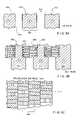
- FIG. 1is a functional diagram of a system for performing the lateral solidification process preferred to implement a preferred process of the present invention
- FIG. 2 ais an illustrative diagram showing a mask having a dashed pattern
- FIG. 2 bis an illustrative diagram of a crystallized silicon film resulting from the use of the mask shown in FIG. 2 a in the system of FIG. 1 ;
- FIG. 3 ais an illustrative diagram showing a mask having a chevron pattern
- FIG. 3 bis an illustrative diagram of a crystallized silicon film resulting from the use of the mask shown in FIG. 3 a in the system of FIG. 1 ;
- FIG. 4 ais an illustrative diagram showing a mask having a line pattern
- FIG. 4 bis an illustrative diagram of a crystallized silicon film resulting from the use of the mask shown in FIG. 4 a in the system of FIG. 1 ;
- FIG. 5 ais an illustrative diagram showing irradiated areas of a silicon sample using a mask having a line pattern
- FIG. 5 bis an illustrative diagram showing irradiated areas of a silicon sample using a mask having a line pattern after initial irradiation and sample translation has occurred;
- FIG. 5 cis an illustrative diagram showing a crystallized silicon film after a second irradiation has occurred
- FIG. 6 ais an illustrative diagram showing a mask having a diagonal line pattern
- FIG. 6 bis an illustrative diagram of a crystallized silicon film resulting from the use of the mask shown in FIG. 6 a in the system of FIG. 1 ;
- FIG. 7 ais an illustrative diagram showing a mask having a sawtooth pattern
- FIG. 7 bis an illustrative diagram of a crystallized silicon film resulting from the use of the mask shown in FIG. 7 a in the system of FIG. 1 ;
- FIG. 8 ais an illustrative diagram showing a mask having a crossing diagonal line pattern
- FIG. 8 bis an illustrative diagram of a crystallized silicon film resulting from the use of the mask shown in FIG. 8 a in the system of FIG. 1 ;
- FIG. 9 ais an illustrative diagram showing a mask having a polka-dot pattern
- FIG. 9 bis an instructive diagram illustrating mask translation using the mask of FIG. 9 a;
- FIG. 9 cis an illustrative diagram of a crystallized silicon film resulting from the use of the mask shown in FIG. 9 a in the system of FIG. 1 using the mask translation scheme shown in FIG. 9 b;
- FIG. 9 dis an illustrative diagram of an alternative crystallized silicon film resulting from the use of the mask shown in FIG. 9 a in the system of FIG. 1 using the mask translation scheme shown in FIG. 9 b ;
- FIG. 10is a flow diagram illustrating the steps implemented in the system of FIG. 1 .
- the present inventionprovides techniques for producing uniform large-grained and grain boundary location controlled polycrystalline thin film semiconductors using the sequential lateral solidification process.
- the sequential lateral solidification processmust first be appreciated.
- the sequential lateral solidification processis a technique for producing large grained silicon structures through small-scale unidirectional translation of a silicon sample in between sequential pulses emitted by an excimer laser. As each pulse is absorbed by the sample, a small area of the sample is caused to melt completely and resolidify laterally into a crystal region produced by the preceding pulses of a pulse set.
- our co-pending patent applicationdescribes as a preferred embodiment a system including excimer laser 110 , energy density modulator 120 to rapidly change the energy density of laser beam 111 , beam attenuator and shutter 130 , optics 140 , 141 , 142 and 143 , beam homogenizer 144 , lens system 145 , 146 , 148 , masking system 150 , lens system 161 , 162 , 163 , incident laser pulse 164 , thin silicon film sample 170 , sample translation stage 180 , granite block 190 , support system 191 , 192 , 193 , 194 , 195 , 196 , and managing computer 100 X and Y direction translation of the silicon sample 170 may be effected by either movement of a mask 210 within masking system 150 or by movement of the sample translation stage 180 under the direction of computer 100 .
- an amorphous silicon thin film sampleis processed into a single or polycrystalline silicon thin film by generating a plurality of excimer laser pulses of a predetermined fluence, controllably modulating the fluence of the excimer laser pulses, homoginizing the modulated laser pulses in a predetermined plane, masking portions of the homoginized modulated laser pulses into patterned beamlets, irradiating an amorphous silicon thin film sample with the patterned beamlets to effect melting of portions thereof corresponding to the beamlets, and controllably translating the sample with respect to the patterned beamlets and with respect to the controlled modulation to thereby process the amorphous silicon thin film sample into a single or polycrystalline silicon thin film by sequential translation of the sample relative to the patterned beamlets and irradiation of the sample by patterned beamlets of varying fluence at corresponding sequential locations thereon.
- FIG. 2 aillustrates a mask 210 incorporating a pattern of slits 220 .
- the mask 210is preferably fabricated from a quartz substrate, and includes either a metallic or dielectric coating which is etched by conventional techniques to form a mask pattern, such as that shown in FIG. 2 a.
- Each slit 220is of a breadth 230 which is chosen in accordance with the necessary dimensionality of the device that will be fabricated on the sample 170 in the particular location that corresponds to the slit 220 .
- the slits 220should be approximately 25 micrometers across to fabricate a 25 micrometer semiconductor device, or in the case of a multi-part device, a channel in a device, in sample 170 .
- the width 240 of the slit 220is preferably between approximately two and five micrometers in order to be small enough to avoid nucleation in sample 170 and large enough to maximize lateral crystal growth for each excimer pulse. It should be understood that although FIG. 2 a illustrates a regular pattern of slits 220 , any pattern of slits could be utilized in accordance with the microstructures desired to be fabricated on film 170 .
- the sample 170is translated with respect to the laser pulses 164 , either by movement of masking system 150 or sample translation stage 180 , in order to grow crystal regions in the sample 170 .
- a processed sample 250 having crystallized regions 260is produced, as shown in FIG. 2 b .
- the breadth 270 of each crystallized regionwill be approximately equal to the breadth 230 in the mask 210 .
- the length 280 of each regionwill be approximately equal to the distance of Y translation effected by movement of the masking system 150 or translation stage 180 , and as with the breadth, should be chosen in accordance with the final device characteristics.
- Each crystal region 260will consist of polysilicon with long and directionally controlled grains.
- FIG. 3 aillustrates a mask 310 incorporating a pattern of chevrons 320 .
- the breadth 320 of each chevron sidewill determine the size of the ultimate single crystal region to be formed in sample 170 .
- a processed sample 350 having crystallized regions 360is produced, as shown in FIG. 3 b .
- Each crystal region 360will consist of a diamond shaped single crystal region 370 and two long grained, directionally controlled polycrystalline silicon regions 380 in the tails of each chevron.
- FIG. 4 aillustrates a mask 410 incorporating a pattern of slits 420 .
- Each slit 410should extend as far across on the mask as the homogenized laser beam 149 incident on the mask permits, and must have a width 440 that is sufficiently narrow to prevent any nucleation from taking place in the irradiated region of sample 170 .
- the width 440will depend on a number of factors, including the energy density of the incident laser pulse, the duration of the incident laser pulse, the thickness of the silicon thin film sample, and the temperature and conductivity of the silicon substrate.
- the slitshould not be more than 2 micrometers wide when a 500 Angstrom film is to be irradiated at room temperature with a laser pulse of 30 ns and having an energy density that slightly exceeds the complete melt threshold of the sample.
- each crystal region 460will consist of long grained, directionally controlled crystals 470 .
- the width of the grains 470will be longer or shorter.
- the Y translation distancemust be smaller than the distance 421 between mask lines, and it is preferred that the translation be at least one micron smaller than this distance 421 to eliminate small crystals that inevitably form at the initial stage of a directionally controlled polycrystalline structure.
- the sample 170is irradiated with one laser pulse.
- the laser pulsewill melt regions 510 , 511 , 512 on the sample, where each melt region is approximately 4 micrometers wide 520 and is spaced approximately 2 micrometers apart 521 .
- This first laser pulsewill induce the formation of crystal growth in the irradiated regions 510 , 511 , 512 , starting from the melt boundaries 530 and proceeding into the melt region, so that polycrystalline silicon 540 forms in the irradiated regions, as shown in FIG. 5 b.
- the sample 170is translated three micrometers in the Y direction and again irradiated with a single excimer laser pulse.
- the second irradiation regions 551 , 552 , 553cause the remaining amorphous silicon 542 and initial crystal regions 543 of the polycrystalline silicon 540 to melt, while leaving the central section 545 of the polycrystalline silicon to remain.
- the crystal structure which forms the central section 545outwardly grows upon solidification of melted regions 542 , 542 , so that a directionally controlled long grained polycrystalline silicon device is formed on sample 170 .
- FIG. 6 aillustrates a mask 610 incorporating a pattern of diagonal lines 620 .
- a processed sample 650 having crystallized regions 660is produced, as shown in FIG. 6 b .
- Each crystal region 660will consist of long grained, directionally controlled crystals 670 .
- the translation distancewill depend on the desired crystal length.
- the process described with reference to FIGS. 5 a–ccould readily be employed using a mask as shown in FIG. 6 a , having 4 micrometer wide lines 620 that are each spaced apart by 2 micrometers.
- This embodimentis especially advantageous in the fabrication of displays or other devices that are oriented with respect to an XY axis, as the polycrystalline structure is not orthogonal to that axis and accordingly, the device performance will be independent of the X or Y coordinates.
- FIG. 7 aillustrates a mask 710 incorporating offset sawtooth wave patterns 720 , 721 .
- a processed sample 750 having crystallized regions 760is produced, as shown in FIG. 7 b .
- Each crystal region 760will consist of a row of hexagonal-rectangular crystals 770 . If the translation distance is slightly greater than the periodicity of the sawtooth pattern, the crystals will be hexagons. This embodiment is beneficial in the generation of larger silicon grains and may increase device performance.
- FIG. 8 aillustrates a mask 810 incorporating a diagonal cross pattern 821 , 822 .
- a processed sample 850 having crystallized regions 860is produced, as shown in FIG. 8 b .
- Each crystal region 860will consist of a row of diamond shaped crystals 870 . If the translation distance is slightly greater than the periodicity of the pattern, the crystals will be squares. This embodiment is also beneficial in the generation of larger silicon grains and may increase device performance.
- FIG. 9 aillustrates a mask 91 0 incorporating a polka-dot pattern 920 .
- the polka-dot mask 910is an inverted mask, where the polka-dots 920 correspond to masked regions and the remainder of the mask 921 is transparent.
- the polka-dot patternmay be sequentially translated about the points on the sample 170 where such crystals are desired. For example, as shown in FIG.
- the polka-dot maskmay be translated 931 a short distance in the positive Y direction after a first laser pulse, a short distance in the positive X direction 932 after a second laser pulse, and a short distance in the negative Y direction 933 after a third laser pulse to induce the formation of large crystals.
- a separation distance between polka-dotsis greater than two times the lateral growth distance, a crystalline structure 950 where crystals 960 separated by small grained polycrystalline silicon regions 961 is generated, as shown in FIG. 9 c .
- the separation distanceis less or equal to two times the lateral growth distance so as to avoid nucleation, a crystalline structure 970 where crystals 980 are generated, as shown in FIG. 9 d.
- FIG. 10is a flow diagram illustrating the basic steps implemented in the system of FIG. 1 .
- the various electronics of the system shown in FIG. 1are initialized 1000 by the computer to initiate the process.
- a thin silicon film sampleis then loaded onto the sample translation stage 1005 . It should be noted that such loading may be either manual or robotically implemented under the control of computer 100 .
- the sample translation stageis moved into an initial position 1015 , which may include an alignment with respect to reference features on the sample.
- the various optical components of the systemare focused 1020 if necessary.
- the laseris then stabilized 1025 to a desired energy level and reputation rate, as needed to fully melt the silicon sample in accordance with the particular processing to be carried out. If necessary, the attenuation of the laser pulses is finely adjusted 1030 .
- the shutteris opened 1035 to expose the sample to a single pulse of irradiation and accordingly, to commence the sequential lateral solidification process.
- the sampleis translated in the X or Y directions 1040 in an amount less than the super lateral grown distance.
- the shutteris again opened 1045 to expose the sample to a single pulse of irradiation, and the sample is again translated in the X or Y directions 1050 in an amount less than the super lateral growth distance.
- the samplewas moved in the X direction in step 1040 , the sample should be moved in the Y direction in Step 1050 in order to create a polka-dot.
- the sampleis then irradiated with a third laser pulse 1055 .
- the process of sample translation and irradiation 1050 , 1055may be repeated 1060 to grow the polka-dot region with four or more laser pulses.
- the sampleis repositioned 1065 , 1066 and the crystallization process is repeated on the new area. If no further areas have been designated for crystallization, the laser is shut off 1070 , the hardware is shut down 1075 , and the process is completed 1080 .
- steps 1005 , 1010 , and 1035 – 1065can be repeated on each sample.
- the thin silicon film sample 170could be replaced by a sample having pre-patterned islands of silicon film.
- the line pattern maskcould be used to grow polycrystalline silicon using two laser pulses as explained with reference to FIGS. 5 a–c , then rotated by 90 degrees and used again in the same process to generate an array of square shaped single crystal silicon.
Landscapes
- Physics & Mathematics (AREA)
- Optics & Photonics (AREA)
- Engineering & Computer Science (AREA)
- General Physics & Mathematics (AREA)
- Microelectronics & Electronic Packaging (AREA)
- Condensed Matter Physics & Semiconductors (AREA)
- Manufacturing & Machinery (AREA)
- Computer Hardware Design (AREA)
- Power Engineering (AREA)
- Plasma & Fusion (AREA)
- Chemical & Material Sciences (AREA)
- Crystallography & Structural Chemistry (AREA)
- Mechanical Engineering (AREA)
- Recrystallisation Techniques (AREA)
Abstract
Description
This application is a continuation application of U.S. application Ser. No. 09/390,535 filed on Sep. 3, 1999 (the “Parent Application”), which has issued as U.S. Pat. No 6,555,449 and is a continuation-in-part of application No. PCT/US96/07730, filed on May 28, 1996, and application Ser. No. 09/200,533, filed on Nov. 27, 1998, which has issued as U.S. Pat. No 6,322,625 the entire disclosures of which are incorporated herein by reference. Thus, the present applications claims priority from the Parent Application under 35 U.S.C. § 120
The U.S. Government has certain rights in this invention pursuant to the terms of the Defense Advanced Research Project Agency award number N66001-98-1-8913.
I. Field of the Invention
The present invention relates to techniques for semiconductor processing, and more particularly to semiconductor processing which may be performed at low temperatures.
II. Description of the Related Art
In the field of semiconductor processing, there have been several attempts to use lasers to convert thin amorphous silicon films into polycrystalline films. For example, in James Im et al., “Crystalline Si Films for Integrated Active-Matrix Liquid-Crystal Displays,” 11 MRS Bullitin 39 (1996), an overview of conventional excimer laser annealing technology is presented. In such a system, an excimer laser beam is shaped into a long beam which is typically up to 30 cm long and 500 micrometers or greater in width. The shaped beam is scanned over a sample of amorphous silicon to facilitate melting thereof and the formation of polycrystalline silicon upon resolidification of the sample.
The use of conventional excimer laser annealing technology to generate polycrystalline silicon is problematic for several reasons. First, the polycrystalline silicon generated in the process is typically small grained, of a random microstructure, and having a nonuniform grain sizes, therefore resulting in poor and nonuniform devices and accordingly, low manufacturing yield. Second, in order to obtain acceptable performance levels, the manufacturing throughput for producing polycrystalline silicon must be kept low. Also, the process generally requires a controlled atmosphere and preheating of the amorphous silicon sample, which leads to a reduction in throughput rates. Accordingly, there exists a need in the field to generate higher quality polycrystalline silicon at greater throughput rates. There likewise exists a need for manufacturing techniques which generate larger and more uniformly microstructured polycrystalline silicon thin films to be used in the fabrication of higher quality devices, such as flat panel displays.
An object of the present invention is to provide techniques for producing uniform large-grained and grain boundary location controlled polycrystalline thin film semiconductors using the sequential lateral solidification process.
A further object of the present invention is to form large-grained and grain boundary location manipulated polycrystalline silicon over substantially the entire semiconductor sample.
Yet another object of the present invention is to provide techniques for the fabrication of semiconductors devices useful for fabricating displays and other products where the predominant orientation of the semiconductor grain boundaries may be controllably aligned or misaligned with respect to the current flow direction of the device.
In order to achieve these objectives as well as others that will become apparent with reference to the following specification, the present invention provides methods for processing an amorphous silicon thin film sample into a polycrystalline silicon thin film are disclosed. In one preferred arrangement, a method includes the steps of generating a sequence of excimer laser pulses, controllably modulating each excimer laser pulse in the sequence to a predetermined fluence, homogenizing each modulated laser pulse in the sequence in a predetermined plane, masking portions of each homogenized fluence controlled laser pulse in the sequence with a two dimensional pattern of slits to generate a sequence of fluence controlled pulses of line patterned beamlets, each slit in the pattern of slits being sufficiently narrow to prevent inducement of significant nucleation in a region of a silicon thin film sample irradiated by a beamlet corresponding to the slit, irradiating an amorphous silicon thin film sample with the sequence of fluence controlled slit patterned beamlets to effect melting of portions thereof corresponding to each fluence controlled patterned beamlet pulse in the sequence of pulses of patterned beamlets, and controllably sequentially translating a relative position of the sample with respect to each of the fluence controlled pulse of slit patterned beamlets to thereby process the amorphous silicon thin film sample into a single or polycrystalline silicon thin film.
In a preferred arrangement, the masking step includes masking portions of each homogenized fluence controlled laser pulse in said sequence with a two dimensional pattern of substantially parallel straight slits spaced a predetermined distance apart and linearly extending parallel to one direction of said plane of homogenization to generate a sequence of fluence controlled pulses of slit patterned beamlets. Advantageously, the translating provides for controllably sequentially translating the relative position of the sample in a direction perpendicular to each of the fluence controlled pulse of slit patterned beamlets over substantially the predetermined slit spacing distance, to thereby process the amorphous silicon thin film sample into polycrystalline silicon thin film having long grained, directionally controlled crystals.
In an especially preferred arrangement, the masking step comprises masking portions of each homoginized fluence controlled laser pulse in the sequence with a two dimensional pattern of substantially parallel straight slits of a predetermined width, spaced a predetermined distance being less than the predetermined width apart, and linearly extending parallel to one direction of the plane of homoginization to generate a sequence of fluence controlled pulses of slit patterned beamlets. In this arrangement, translating step comprises translating by a distance less than the predetermined width the relative position of the sample in a direction perpendicular to each of the fluence controlled pulse of slit patterned beamlets, to the to thereby process the amorphous silicon thin film sample into polycrystalline silicon thin film having long grained, directionally controlled crystals using just two laser pulses. In one exemplary embodiment, the predetermined width is approximately 4 micrometers, the predetermined spacing distance is approximately 2 micrometers, and the translating distance is approximately 3 micrometers.
In an alternative preferred arrangement, the masking step comprises masking portions of each homoginized fluence controlled laser pulse in the sequence with a two dimensional pattern of substantially parallel straight slits spaced a predetermined distance apart and linearly extending at substantially 45 degree angle with respect to one direction of the plane of homoginization to generate a sequence of fluence controlled pulses of slit patterned beamlets. In this arrangement, the translating step provides for controllably sequentially translating the relative position of the sample in a direction parallel to the one direction of the plane of homoginization over substantially the predetermined slit distance, to thereby process the amorphous silicon thin film sample into polycrystalline silicon thin film having long grained, directionally controlled crystals that are disoriented with respect to the XY axis of the thin silicon film.
In yet another preferred arrangement, the masking step comprises masking portions of each homoginized fluence controlled laser pulse in the sequence with a two dimensional pattern of intersecting straight slits, a first group of straight slits being spaced a first predetermined apart and linearly extending at substantially 45 degree angle with respect to a first direction of the plane of homoginization, and a second group of straight slits being spaced a second predetermined distance apart and linearly extending at substantially 45 degree angle with respect to a second direction of the plane of homoginization and intersecting the first group at substantially a 90 degree angle, to generate a sequence of fluence controlled pulses of slit patterned beamlets. The corresponding translating step provides for controllably sequentially translating the relative position of the sample in a direction parallel to the first direction of the plane of homoginization over substantially the first predetermined slit spacing distance, to thereby process the amorphous silicon thin film sample into polycrystalline silicon thin film having large diamond shaped crystals.
In still another alternative arrangement, the masking step comprises masking portions of each homoginized fluence controlled laser pulse in the sequence with a two dimensional pattern of sawtooth shaped slits spaced a predetermined distance apart and extending generally parallel to one direction of the plane of homogenization to generate a sequence of fluence controlled pulses of slit patterned beamlets. In this arrangement, the translating step provides for controllably sequentially translating the relative position of the sample in a direction perpendicular to each of the fluence controlled pulse of slit patterned beamlets over substantially the predetermined slit spacing distance, to the to thereby process the amorphous silicon thin film sample into polycrystalline silicon thin film having large hexagonal crystals.
In a modified arrangement, an alternative technique for processing an amorphous silicon thin film sample into a polycrystalline silicon thin film using a polka-dot pattern is provided. The technique includes generating a sequence of excimer laser pulses, homogenizing each laser pulse in the sequence in a predetermined plane, masking portions of each homogenized laser pulse in the sequence with a two dimensional pattern of substantially opaque dots to generate a sequence of pulses of dot patterned beamlets, irradiating an amorphous silicon thin film sample with the sequence of dot patterned beamlets to effect melting of portions thereof corresponding to each dot patterned beamlet pulse in the sequence of pulses of patterned beamlets, and controllably sequentially translating the sample relative to each of the pulses of dot patterned beamlets by alternating a translation direction in two perpendicular axis and in a distance less than the super lateral grown distance for the sample, to thereby process the amorphous silicon thin film sample into a polycrystalline silicon thin film.
The accompanying drawings, which are incorporated and constitute part of this disclosure, illustrate a preferred embodiment of the invention and serve to explain the principles of the invention.
The present invention provides techniques for producing uniform large-grained and grain boundary location controlled polycrystalline thin film semiconductors using the sequential lateral solidification process. In order to fully understand those techniques, the sequential lateral solidification process must first be appreciated.
The sequential lateral solidification process is a technique for producing large grained silicon structures through small-scale unidirectional translation of a silicon sample in between sequential pulses emitted by an excimer laser. As each pulse is absorbed by the sample, a small area of the sample is caused to melt completely and resolidify laterally into a crystal region produced by the preceding pulses of a pulse set.
A particularly advantageous sequential lateral solidification process and an apparatus to carry out that process are disclosed in our co-pending patent application entitled “Systems and Methods using Sequential Lateral Solidification for Producing Single or Polycrystalline Silicon Thin Films at Low Temperatures,” filed concurrently with the present application and assigned to the common assignee, the disclosure of which is incorporated by reference herein. While the foregoing disclosure is made with reference to the particular techniques described in our co-pending patent application, it should be understood that other sequential lateral solidification techniques could readily be adapted for use in the present invention.
With reference toFIG. 1 , our co-pending patent application describes as a preferred embodiment a system includingexcimer laser 110,energy density modulator 120 to rapidly change the energy density oflaser beam 111, beam attenuator andshutter 130,optics beam homogenizer 144,lens system system 150,lens system incident laser pulse 164, thinsilicon film sample 170,sample translation stage 180,granite block 190,support system silicon sample 170 may be effected by either movement of amask 210 within maskingsystem 150 or by movement of thesample translation stage 180 under the direction ofcomputer 100.
As described in further detail in our co-pending application, an amorphous silicon thin film sample is processed into a single or polycrystalline silicon thin film by generating a plurality of excimer laser pulses of a predetermined fluence, controllably modulating the fluence of the excimer laser pulses, homoginizing the modulated laser pulses in a predetermined plane, masking portions of the homoginized modulated laser pulses into patterned beamlets, irradiating an amorphous silicon thin film sample with the patterned beamlets to effect melting of portions thereof corresponding to the beamlets, and controllably translating the sample with respect to the patterned beamlets and with respect to the controlled modulation to thereby process the amorphous silicon thin film sample into a single or polycrystalline silicon thin film by sequential translation of the sample relative to the patterned beamlets and irradiation of the sample by patterned beamlets of varying fluence at corresponding sequential locations thereon. The following embodiments of the present invention will now be described with reference to the foregoing processing technique.
Referring toFIGS. 2 aandb,a first embodiment of the present invention will now be described.FIG. 2 aillustrates amask 210 incorporating a pattern ofslits 220. Themask 210 is preferably fabricated from a quartz substrate, and includes either a metallic or dielectric coating which is etched by conventional techniques to form a mask pattern, such as that shown inFIG. 2 a.Eachslit 220 is of abreadth 230 which is chosen in accordance with the necessary dimensionality of the device that will be fabricated on thesample 170 in the particular location that corresponds to theslit 220. —For example, theslits 220 should be approximately 25 micrometers across to fabricate a25 micrometer semiconductor device, or in the case of a multi-part device, a channel in a device, insample 170. Thewidth 240 of theslit 220 is preferably between approximately two and five micrometers in order to be small enough to avoid nucleation insample 170 and large enough to maximize lateral crystal growth for each excimer pulse. It should be understood that althoughFIG. 2 aillustrates a regular pattern ofslits 220, any pattern of slits could be utilized in accordance with the microstructures desired to be fabricated onfilm 170.
In accordance with the present invention, thesample 170 is translated with respect to thelaser pulses 164, either by movement of maskingsystem 150 orsample translation stage 180, in order to grow crystal regions in thesample 170. When thesample 170 is translated in the Y direction andmask 210 is used in maskingsystem 150, a processedsample 250 having crystallizedregions 260 is produced, as shown inFIG. 2 b. Thebreadth 270 of each crystallized region will be approximately equal to thebreadth 230 in themask 210. Thelength 280 of each region will be approximately equal to the distance of Y translation effected by movement of themasking system 150 ortranslation stage 180, and as with the breadth, should be chosen in accordance with the final device characteristics. Eachcrystal region 260 will consist of polysilicon with long and directionally controlled grains.
Referring next toFIGS. 3 aandb, a second embodiment of the present invention will now be described.FIG. 3 aillustrates amask 310 incorporating a pattern ofchevrons 320. Thebreadth 320 of each chevron side will determine the size of the ultimate single crystal region to be formed insample 170. When thesample 170 is translated in the Y direction andmask 310 is used in maskingsystem 150, a processedsample 350 having crystallizedregions 360 is produced, as shown inFIG. 3 b. Eachcrystal region 360 will consist of a diamond shapedsingle crystal region 370 and two long grained, directionally controlledpolycrystalline silicon regions 380 in the tails of each chevron.
While the embodiments described with reference toFIGS. 2 and 3 are advantageous to generate spatially separated devices onsilicon sample 170, at least some of thesilicon sample 170 is not utilized in the final semiconductor. In order to facilitate a more flexible configuration of devices that can be developed on thesemiconductor sample 170, the following preferred embodiments will now be described.
Referring toFIGS. 4 aandb,a third embodiment of the present invention will now be described.FIG. 4 aillustrates amask 410 incorporating a pattern ofslits 420. Eachslit 410 should extend as far across on the mask as thehomogenized laser beam 149 incident on the mask permits, and must have awidth 440 that is sufficiently narrow to prevent any nucleation from taking place in the irradiated region ofsample 170. Thewidth 440 will depend on a number of factors, including the energy density of the incident laser pulse, the duration of the incident laser pulse, the thickness of the silicon thin film sample, and the temperature and conductivity of the silicon substrate. For example, the slit should not be more than 2 micrometers wide when a 500 Angstrom film is to be irradiated at room temperature with a laser pulse of 30 ns and having an energy density that slightly exceeds the complete melt threshold of the sample.
When thesample 170 is translated in the Y direction andmask 410 is used in maskingsystem 150, a fabricatedsample 450 having crystallizedregions 460 is generated, as shown inFIG. 4 b.Eachcrystal region 460 will consist of long grained, directionally controlledcrystals 470. Depending on theperiodicity 421 of themasking lines 420 insample 410, the width of thegrains 470 will be longer or shorter. In order to prevent amorphous silicon regions from being left onsample 170, the Y translation distance must be smaller than thedistance 421 between mask lines, and it is preferred that the translation be at least one micron smaller than thisdistance 421 to eliminate small crystals that inevitably form at the initial stage of a directionally controlled polycrystalline structure.
An especially preferred technique using a mask having a pattern of lines will next be described. Using a mask as shown inFIG. 4 awhere closelypacked mask lines 420 having awidth 440 of 4 micrometers are each spaced 2 micrometers apart, thesample 170 is irradiated with one laser pulse. As shown inFIG. 5 a, the laser pulse will meltregions irradiated regions melt boundaries 530 and proceeding into the melt region, so thatpolycrystalline silicon 540 forms in the irradiated regions, as shown inFIG. 5 b.
In order to eliminate the numerous smallinitial crystals 541 that form at themelt boundaries 530, thesample 170 is translated three micrometers in the Y direction and again irradiated with a single excimer laser pulse. Thesecond irradiation regions amorphous silicon 542 andinitial crystal regions 543 of thepolycrystalline silicon 540 to melt, while leaving thecentral section 545 of the polycrystalline silicon to remain. As shown inFIG. 5 c, the crystal structure which forms thecentral section 545 outwardly grows upon solidification of meltedregions sample 170.
Referring toFIGS. 6 aandb, a fourth embodiment of the present invention will now be described.FIG. 6 aillustrates amask 610 incorporating a pattern ofdiagonal lines 620. When thesample 170 is translated in the Y direction andmask 610 is used in maskingsystem 150, a processedsample 650 having crystallized regions660 is produced, as shown inFIG. 6 b. Each crystal region660 will consist of long grained, directionally controlled crystals670.
As with the embodiment described above with respect toFIGS. 4 aandb, the translation distance will depend on the desired crystal length. Also, the process described with reference toFIGS. 5 a–ccould readily be employed using a mask as shown inFIG. 6 a, having 4 micrometerwide lines 620 that are each spaced apart by 2 micrometers. This embodiment is especially advantageous in the fabrication of displays or other devices that are oriented with respect to an XY axis, as the polycrystalline structure is not orthogonal to that axis and accordingly, the device performance will be independent of the X or Y coordinates.
Referring next toFIGS. 7 aandb, a fifth embodiment of the present invention will now be described.FIG. 7 aillustrates amask 710 incorporating offsetsawtooth wave patterns sample 170 is translated in the Y direction andmask 710 is used in maskingsystem 150, a processedsample 750 having crystallizedregions 760 is produced, as shown inFIG. 7 b. Eachcrystal region 760 will consist of a row of hexagonal-rectangular crystals 770. If the translation distance is slightly greater than the periodicity of the sawtooth pattern, the crystals will be hexagons. This embodiment is beneficial in the generation of larger silicon grains and may increase device performance.
Referring next toFIGS. 8 aandb, a sixth embodiment of the present invention will now be described.FIG. 8 aillustrates amask 810 incorporating adiagonal cross pattern 821,822. When thesample 170 is translated in the Y direction andmask 810 is used in maskingsystem 150, a processedsample 850 having crystallizedregions 860 is produced, as shown inFIG. 8 b. Eachcrystal region 860 will consist of a row of diamond shapedcrystals 870. If the translation distance is slightly greater than the periodicity of the pattern, the crystals will be squares. This embodiment is also beneficial in the generation of larger silicon grains and may increase device performance.
Referring next toFIGS. 9 a–d, a seventh embodiment of the present invention will now be described.FIG. 9 aillustrates a mask910 incorporating a polka-dot pattern 920. The polka-dot mask 910 is an inverted mask, where the polka-dots 920 correspond to masked regions and the remainder of themask 921 is transparent. In order to fabricate large silicon crystals, the polka-dot pattern may be sequentially translated about the points on thesample 170 where such crystals are desired. For example, as shown inFIG. 9 b, the polka-dot mask may be translated931 a short distance in the positive Y direction after a first laser pulse, a short distance in thepositive X direction 932 after a second laser pulse, and a short distance in thenegative Y direction 933 after a third laser pulse to induce the formation of large crystals. If the separation distance between polka-dots is greater than two times the lateral growth distance, acrystalline structure 950 wherecrystals 960 separated by small grainedpolycrystalline silicon regions 961 is generated, as shown inFIG. 9 c. If the separation distance is less or equal to two times the lateral growth distance so as to avoid nucleation, acrystalline structure 970 wherecrystals 980 are generated, as shown inFIG. 9 d.
Referring next toFIG. 10 , the steps executed bycomputer 100 to control the crystal growth process implemented with respect toFIG. 9 will be described.FIG. 10 is a flow diagram illustrating the basic steps implemented in the system ofFIG. 1 . The various electronics of the system shown inFIG. 1 are initialized1000 by the computer to initiate the process. A thin silicon film sample is then loaded onto thesample translation stage 1005. It should be noted that such loading may be either manual or robotically implemented under the control ofcomputer 100. Next, the sample translation stage is moved into aninitial position 1015, which may include an alignment with respect to reference features on the sample. The various optical components of the system are focused1020 if necessary. The laser is then stabilized1025 to a desired energy level and reputation rate, as needed to fully melt the silicon sample in accordance with the particular processing to be carried out. If necessary, the attenuation of the laser pulses is finely adjusted1030.
Next, the shutter is opened1035 to expose the sample to a single pulse of irradiation and accordingly, to commence the sequential lateral solidification process. The sample is translated in the X orY directions 1040 in an amount less than the super lateral grown distance. The shutter is again opened1045 to expose the sample to a single pulse of irradiation, and the sample is again translated in the X orY directions 1050 in an amount less than the super lateral growth distance. Of course, if the sample was moved in the X direction instep 1040, the sample should be moved in the Y direction inStep 1050 in order to create a polka-dot. The sample is then irradiated with athird laser pulse 1055. The process of sample translation andirradiation
Next, if other areas on the sample have been designated for crystallization, the sample is repositioned1065,1066 and the crystallization process is repeated on the new area. If no further areas have been designated for crystallization, the laser is shut off1070, the hardware is shut down1075, and the process is completed1080. Of course, if processing of additional samples is desired or if the present invention is utilized for batch processing,steps
The foregoing merely illustrates the principles of the invention. Various modifications and alterations to the described embodiments will be apparent to those skilled in the art in view of the teachings herein. For example, the thinsilicon film sample 170 could be replaced by a sample having pre-patterned islands of silicon film. Also, the line pattern mask could be used to grow polycrystalline silicon using two laser pulses as explained with reference toFIGS. 5 a–c, then rotated by 90 degrees and used again in the same process to generate an array of square shaped single crystal silicon. It will thus be appreciated that those skilled in the art will be able to devise numerous systems and methods which, although not explicitly shown or described herein, embody the principles of the invention and are thus within the spirit and scope of the invention.
Claims (8)
1. A method of annealing a silicon film having an interface with an underlying surface, comprising:
growing a silicon grain having a length by completely melting a section of the silicon film to the interface using a first shot of a laser beam having a beam width that is greater than the length of the silicon grain, but less than twice the length of the silicon grain; and
increasing the length of the grown silicon grain by completely remelting part of the grown silicon grain using a second shot of the laser beam, wherein the remelted part is determined by displacing the laser beam relative to the substrate more than one-half of the beam width of the laser beam.
2. The method of annealing a silicon film according toclaim 1 , wherein the silicon film is scanned by the laser beam.
3. The method of annealing a silicon film according toclaim 2 , wherein the silicon film is scanned by repeated steps of growing silicon grains, displacing the laser beam relative to the silicon film, remelting part of the grown silicon grains, and then again displacing the laser beam relative to the silicon film.
4. The method of annealing a silicon film according toclaim 1 , wherein the length of the silicon grain grown by the first shot of the laser beam is about 2 to 4 micrometers.
5. The method of annealing a silicon film according toclaim 4 , wherein the length of the silicon grain is increased to about 4 to 8 micrometers by the second shot of the laser beam.
6. The method of annealing a silicon film according toclaim 1 , wherein the silicon film is amorphous silicon before the first shot of the laser beam.
7. The method of annealing a silicon film according toclaim 1 , wherein the silicon grain is grown and lengthened at atmospheric pressure.
8. The method of annealing a silicon film according toclaim 1 , wherein the laser beam has a beam width less than 10 micrometers.
Priority Applications (7)
| Application Number | Priority Date | Filing Date | Title |
|---|---|---|---|
| US10/294,001US7029996B2 (en) | 1999-09-03 | 2002-11-13 | Methods for producing uniform large-grained and grain boundary location manipulated polycrystalline thin film semiconductors using sequential lateral solidification |
| US11/141,815US7319056B2 (en) | 1996-05-28 | 2005-06-01 | Methods for producing uniform large-grained and grain boundary location manipulated polycrystalline thin film semiconductors using sequential lateral solidification |
| US11/744,493US7679028B2 (en) | 1996-05-28 | 2007-05-04 | Methods for producing uniform large-grained and grain boundary location manipulated polycrystalline thin film semiconductors using sequential lateral solidification |
| US12/402,208US8859436B2 (en) | 1996-05-28 | 2009-03-11 | Uniform large-grained and grain boundary location manipulated polycrystalline thin film semiconductors formed using sequential lateral solidification and devices formed thereon |
| US12/419,821US8680427B2 (en) | 1996-05-28 | 2009-04-07 | Uniform large-grained and gain boundary location manipulated polycrystalline thin film semiconductors formed using sequential lateral solidification and devices formed thereon |
| US12/567,414US8278659B2 (en) | 1996-05-28 | 2009-09-25 | Uniform large-grained and grain boundary location manipulated polycrystalline thin film semiconductors formed using sequential lateral solidification and devices formed thereon |
| US13/596,693US20130009074A1 (en) | 1996-05-28 | 2012-08-28 | Uniform large-grained and grain boundary location manipulated polycrystalline thin film semiconductors formed using sequential lateral solidification and devices formed thereon |
Applications Claiming Priority (2)
| Application Number | Priority Date | Filing Date | Title |
|---|---|---|---|
| US09/390,535US6555449B1 (en) | 1996-05-28 | 1999-09-03 | Methods for producing uniform large-grained and grain boundary location manipulated polycrystalline thin film semiconductors using sequential lateral solidfication |
| US10/294,001US7029996B2 (en) | 1999-09-03 | 2002-11-13 | Methods for producing uniform large-grained and grain boundary location manipulated polycrystalline thin film semiconductors using sequential lateral solidification |
Related Parent Applications (4)
| Application Number | Title | Priority Date | Filing Date |
|---|---|---|---|
| PCT/US1996/007730Continuation-In-PartWO1997045827A1 (en) | 1996-05-28 | 1996-05-28 | Crystallization processing of semiconductor film regions on a substrate, and devices made therewith |
| US09/200,533Continuation-In-PartUS6322625B2 (en) | 1996-05-28 | 1998-11-27 | Crystallization processing of semiconductor film regions on a substrate, and devices made therewith |
| US09/390,535ContinuationUS6555449B1 (en) | 1996-05-28 | 1999-09-03 | Methods for producing uniform large-grained and grain boundary location manipulated polycrystalline thin film semiconductors using sequential lateral solidfication |
| US11/744,493ContinuationUS7679028B2 (en) | 1996-05-28 | 2007-05-04 | Methods for producing uniform large-grained and grain boundary location manipulated polycrystalline thin film semiconductors using sequential lateral solidification |
Related Child Applications (1)
| Application Number | Title | Priority Date | Filing Date |
|---|---|---|---|
| US11/141,815ContinuationUS7319056B2 (en) | 1996-05-28 | 2005-06-01 | Methods for producing uniform large-grained and grain boundary location manipulated polycrystalline thin film semiconductors using sequential lateral solidification |
Publications (2)
| Publication Number | Publication Date |
|---|---|
| US20030096489A1 US20030096489A1 (en) | 2003-05-22 |
| US7029996B2true US7029996B2 (en) | 2006-04-18 |
Family
ID=23542857
Family Applications (9)
| Application Number | Title | Priority Date | Filing Date |
|---|---|---|---|
| US09/390,535Expired - LifetimeUS6555449B1 (en) | 1996-05-28 | 1999-09-03 | Methods for producing uniform large-grained and grain boundary location manipulated polycrystalline thin film semiconductors using sequential lateral solidfication |
| US10/294,001Expired - Fee RelatedUS7029996B2 (en) | 1996-05-28 | 2002-11-13 | Methods for producing uniform large-grained and grain boundary location manipulated polycrystalline thin film semiconductors using sequential lateral solidification |
| US10/308,958AbandonedUS20030119286A1 (en) | 1996-05-28 | 2002-12-03 | Method for producing uniform large-grained and grain boundary location manipulated polycrystalline thin film semiconductors using sequential lateral solidification |
| US11/141,815Expired - Fee RelatedUS7319056B2 (en) | 1996-05-28 | 2005-06-01 | Methods for producing uniform large-grained and grain boundary location manipulated polycrystalline thin film semiconductors using sequential lateral solidification |
| US11/744,493Expired - Fee RelatedUS7679028B2 (en) | 1996-05-28 | 2007-05-04 | Methods for producing uniform large-grained and grain boundary location manipulated polycrystalline thin film semiconductors using sequential lateral solidification |
| US12/402,208Expired - Fee RelatedUS8859436B2 (en) | 1996-05-28 | 2009-03-11 | Uniform large-grained and grain boundary location manipulated polycrystalline thin film semiconductors formed using sequential lateral solidification and devices formed thereon |
| US12/419,821Expired - Fee RelatedUS8680427B2 (en) | 1996-05-28 | 2009-04-07 | Uniform large-grained and gain boundary location manipulated polycrystalline thin film semiconductors formed using sequential lateral solidification and devices formed thereon |
| US12/567,414Expired - Fee RelatedUS8278659B2 (en) | 1996-05-28 | 2009-09-25 | Uniform large-grained and grain boundary location manipulated polycrystalline thin film semiconductors formed using sequential lateral solidification and devices formed thereon |
| US13/596,693AbandonedUS20130009074A1 (en) | 1996-05-28 | 2012-08-28 | Uniform large-grained and grain boundary location manipulated polycrystalline thin film semiconductors formed using sequential lateral solidification and devices formed thereon |
Family Applications Before (1)
| Application Number | Title | Priority Date | Filing Date |
|---|---|---|---|
| US09/390,535Expired - LifetimeUS6555449B1 (en) | 1996-05-28 | 1999-09-03 | Methods for producing uniform large-grained and grain boundary location manipulated polycrystalline thin film semiconductors using sequential lateral solidfication |
Family Applications After (7)
| Application Number | Title | Priority Date | Filing Date |
|---|---|---|---|
| US10/308,958AbandonedUS20030119286A1 (en) | 1996-05-28 | 2002-12-03 | Method for producing uniform large-grained and grain boundary location manipulated polycrystalline thin film semiconductors using sequential lateral solidification |
| US11/141,815Expired - Fee RelatedUS7319056B2 (en) | 1996-05-28 | 2005-06-01 | Methods for producing uniform large-grained and grain boundary location manipulated polycrystalline thin film semiconductors using sequential lateral solidification |
| US11/744,493Expired - Fee RelatedUS7679028B2 (en) | 1996-05-28 | 2007-05-04 | Methods for producing uniform large-grained and grain boundary location manipulated polycrystalline thin film semiconductors using sequential lateral solidification |
| US12/402,208Expired - Fee RelatedUS8859436B2 (en) | 1996-05-28 | 2009-03-11 | Uniform large-grained and grain boundary location manipulated polycrystalline thin film semiconductors formed using sequential lateral solidification and devices formed thereon |
| US12/419,821Expired - Fee RelatedUS8680427B2 (en) | 1996-05-28 | 2009-04-07 | Uniform large-grained and gain boundary location manipulated polycrystalline thin film semiconductors formed using sequential lateral solidification and devices formed thereon |
| US12/567,414Expired - Fee RelatedUS8278659B2 (en) | 1996-05-28 | 2009-09-25 | Uniform large-grained and grain boundary location manipulated polycrystalline thin film semiconductors formed using sequential lateral solidification and devices formed thereon |
| US13/596,693AbandonedUS20130009074A1 (en) | 1996-05-28 | 2012-08-28 | Uniform large-grained and grain boundary location manipulated polycrystalline thin film semiconductors formed using sequential lateral solidification and devices formed thereon |
Country Status (10)
| Country | Link |
|---|---|
| US (9) | US6555449B1 (en) |
| EP (2) | EP1212784A4 (en) |
| JP (1) | JP4551045B2 (en) |
| KR (1) | KR100647751B1 (en) |
| CN (1) | CN1235268C (en) |
| AU (1) | AU7573600A (en) |
| CA (1) | CA2385119C (en) |
| MX (1) | MXPA02002332A (en) |
| SG (1) | SG146418A1 (en) |
| WO (1) | WO2001018854A1 (en) |
Cited By (36)
| Publication number | Priority date | Publication date | Assignee | Title |
|---|---|---|---|---|
| US20040203219A1 (en)* | 1999-08-18 | 2004-10-14 | Semiconductor Energy Laboratory Co., Ltd. | Laser apparatus and laser annealing method |
| US20050285120A1 (en)* | 2003-03-05 | 2005-12-29 | Samsung Sdi Co., Ltd. | Polycrystalline silicon thin film, fabrication method thereof, and thin film transistor without directional dependency on active channels fabricated using the same |
| US20060065186A1 (en)* | 2002-12-10 | 2006-03-30 | Canon Kabushiki Kaisha | Process for producing crystalline thin film |
| US20060102901A1 (en)* | 2004-11-18 | 2006-05-18 | The Trustees Of Columbia University In The City Of New York | Systems and methods for creating crystallographic-orientation controlled poly-Silicon films |
| US20060254500A1 (en)* | 2005-04-06 | 2006-11-16 | The Trustees Of Columbia University In The City Of New York | Line scan sequential lateral solidification of thin films |
| US20070048978A1 (en)* | 2005-08-23 | 2007-03-01 | Au Optronics Corp. | Mask for sequential lateral solidification (SLS) process and a method thereof |
| US20080072953A1 (en)* | 2006-09-27 | 2008-03-27 | Thinsilicon Corp. | Back contact device for photovoltaic cells and method of manufacturing a back contact device |
| US20080176414A1 (en)* | 2003-09-16 | 2008-07-24 | Columbia University | Systems and methods for inducing crystallization of thin films using multiple optical paths |
| US20080295882A1 (en)* | 2007-05-31 | 2008-12-04 | Thinsilicon Corporation | Photovoltaic device and method of manufacturing photovoltaic devices |
| US20090001523A1 (en)* | 2005-12-05 | 2009-01-01 | Im James S | Systems and Methods for Processing a Film, and Thin Films |
| US20090045181A1 (en)* | 2003-09-16 | 2009-02-19 | The Trustees Of Columbia University In The City Of New York | Systems and methods for processing thin films |
| US20090078940A1 (en)* | 2007-09-26 | 2009-03-26 | Sharp Laboratories Of America, Inc. | Location-controlled crystal seeding |
| US20090218577A1 (en)* | 2005-08-16 | 2009-09-03 | Im James S | High throughput crystallization of thin films |
| US20090242805A1 (en)* | 2005-08-16 | 2009-10-01 | Im James S | Systems and methods for uniform sequential lateral solidification of thin films using high frequency lasers |
| US20100187529A1 (en)* | 2003-09-16 | 2010-07-29 | Columbia University | Laser-irradiated thin films having variable thickness |
| US20100282314A1 (en)* | 2009-05-06 | 2010-11-11 | Thinsilicion Corporation | Photovoltaic cells and methods to enhance light trapping in semiconductor layer stacks |
| US20100313952A1 (en)* | 2009-06-10 | 2010-12-16 | Thinsilicion Corporation | Photovoltaic modules and methods of manufacturing photovoltaic modules having multiple semiconductor layer stacks |
| US20110101368A1 (en)* | 2008-02-29 | 2011-05-05 | The Trustees Of Columbia University In The City Of New York | Flash lamp annealing crystallization for large area thin films |
| US20110108108A1 (en)* | 2008-02-29 | 2011-05-12 | The Trustees Of Columbia University In The City Of | Flash light annealing for thin films |
| US20110114156A1 (en)* | 2009-06-10 | 2011-05-19 | Thinsilicon Corporation | Photovoltaic modules having a built-in bypass diode and methods for manufacturing photovoltaic modules having a built-in bypass diode |
| US20110121306A1 (en)* | 2009-11-24 | 2011-05-26 | The Trustees Of Columbia University In The City Of New York | Systems and Methods for Non-Periodic Pulse Sequential Lateral Solidification |
| US20110175099A1 (en)* | 2008-02-29 | 2011-07-21 | The Trustees Of Columbia University In The City Of New York | Lithographic method of making uniform crystalline si films |
| US8012861B2 (en) | 2007-11-21 | 2011-09-06 | The Trustees Of Columbia University In The City Of New York | Systems and methods for preparing epitaxially textured polycrystalline films |
| US20110220625A1 (en)* | 2010-03-15 | 2011-09-15 | Christoph Pluss | Laser machining apparatus and method for the manufacture of a rotationally symmetrical tool |
| US20110248278A1 (en)* | 2003-09-19 | 2011-10-13 | Im James S | Single scan irradiation for crystallization of thin films |
| US8063338B2 (en) | 2003-09-16 | 2011-11-22 | The Trustees Of Columbia In The City Of New York | Enhancing the width of polycrystalline grains with mask |
| US8265109B2 (en) | 2002-05-07 | 2012-09-11 | Cymer, Inc. | Systems and methods for implementing an interaction between a laser shaped as line beam and a film deposited on a substrate |
| US8278659B2 (en) | 1996-05-28 | 2012-10-02 | The Trustees Of Columbia University In The City Of New York | Uniform large-grained and grain boundary location manipulated polycrystalline thin film semiconductors formed using sequential lateral solidification and devices formed thereon |
| US8411713B2 (en) | 2002-08-19 | 2013-04-02 | The Trustees Of Columbia University In The City Of New York | Process and system for laser crystallization processing of film regions on a substrate to minimize edge areas, and structure of such film regions |
| US8415670B2 (en) | 2007-09-25 | 2013-04-09 | The Trustees Of Columbia University In The City Of New York | Methods of producing high uniformity in thin film transistor devices fabricated on laterally crystallized thin films |
| US8426296B2 (en) | 2007-11-21 | 2013-04-23 | The Trustees Of Columbia University In The City Of New York | Systems and methods for preparing epitaxially textured polycrystalline films |
| US8557040B2 (en) | 2007-11-21 | 2013-10-15 | The Trustees Of Columbia University In The City Of New York | Systems and methods for preparation of epitaxially textured thick films |
| US8614471B2 (en) | 2007-09-21 | 2013-12-24 | The Trustees Of Columbia University In The City Of New York | Collections of laterally crystallized semiconductor islands for use in thin film transistors |
| US8802580B2 (en) | 2008-11-14 | 2014-08-12 | The Trustees Of Columbia University In The City Of New York | Systems and methods for the crystallization of thin films |
| US9087696B2 (en) | 2009-11-03 | 2015-07-21 | The Trustees Of Columbia University In The City Of New York | Systems and methods for non-periodic pulse partial melt film processing |
| US9646831B2 (en) | 2009-11-03 | 2017-05-09 | The Trustees Of Columbia University In The City Of New York | Advanced excimer laser annealing for thin films |
Families Citing this family (82)
| Publication number | Priority date | Publication date | Assignee | Title |
|---|---|---|---|---|
| US6573531B1 (en) | 1999-09-03 | 2003-06-03 | The Trustees Of Columbia University In The City Of New York | Systems and methods using sequential lateral solidification for producing single or polycrystalline silicon thin films at low temperatures |
| US6830993B1 (en)* | 2000-03-21 | 2004-12-14 | The Trustees Of Columbia University In The City Of New York | Surface planarization of thin silicon films during and after processing by the sequential lateral solidification method |
| KR100854834B1 (en) | 2000-10-10 | 2008-08-27 | 더 트러스티스 오브 컬럼비아 유니버시티 인 더 시티 오브 뉴욕 | Method and apparatus for processing thin metal layers |
| US6961117B2 (en)* | 2000-11-27 | 2005-11-01 | The Trustees Of Columbia University In The City Of New York | Process and mask projection system for laser crystallization processing of semiconductor film regions on a substrate |
| KR100400510B1 (en)* | 2000-12-28 | 2003-10-08 | 엘지.필립스 엘시디 주식회사 | A machine for Si crystallization and method of crystallizing Si |
| KR100672628B1 (en)* | 2000-12-29 | 2007-01-23 | 엘지.필립스 엘시디 주식회사 | Active Matrix Organic Electroluminescent Display Device |
| US7128825B2 (en)* | 2001-03-14 | 2006-10-31 | Applied Materials, Inc. | Method and composition for polishing a substrate |
| US7009140B2 (en)* | 2001-04-18 | 2006-03-07 | Cymer, Inc. | Laser thin film poly-silicon annealing optical system |
| US7061959B2 (en)* | 2001-04-18 | 2006-06-13 | Tcz Gmbh | Laser thin film poly-silicon annealing system |
| WO2002086954A1 (en)* | 2001-04-19 | 2002-10-31 | The Trustee Of Columbia University In The City Of New York | Method and system for providing a single-scan, continuous motion sequential lateral solidification |
| KR100405080B1 (en)* | 2001-05-11 | 2003-11-10 | 엘지.필립스 엘시디 주식회사 | A method of crystallizing Si |
| JP4310076B2 (en)* | 2001-05-31 | 2009-08-05 | キヤノン株式会社 | Method for producing crystalline thin film |
| JP4109026B2 (en)* | 2001-07-27 | 2008-06-25 | 東芝松下ディスプレイテクノロジー株式会社 | Method for manufacturing array substrate and photomask |
| US7088758B2 (en) | 2001-07-27 | 2006-08-08 | Cymer, Inc. | Relax gas discharge laser lithography light source |
| TW527732B (en)* | 2001-08-21 | 2003-04-11 | Samsung Electronics Co Ltd | Masks for forming polysilicon and methods for manufacturing thin film transistor using the masks |
| TW556350B (en)* | 2001-08-27 | 2003-10-01 | Univ Columbia | A method to increase device-to-device uniformity for polycrystalline thin-film transistors by deliberately mis-aligning the microstructure relative to the channel region |
| SG143981A1 (en)* | 2001-08-31 | 2008-07-29 | Semiconductor Energy Lab | Laser irradiation method, laser irradiation apparatus, and method of manufacturing a semiconductor device |
| US6767804B2 (en)* | 2001-11-08 | 2004-07-27 | Sharp Laboratories Of America, Inc. | 2N mask design and method of sequential lateral solidification |
| KR100462862B1 (en)* | 2002-01-18 | 2004-12-17 | 삼성에스디아이 주식회사 | Polysilicon thin layer for thin film transistor and device using thereof |
| JP4279498B2 (en) | 2002-02-28 | 2009-06-17 | 株式会社 液晶先端技術開発センター | Semiconductor thin film forming method, semiconductor thin film forming apparatus, and crystallization method |
| US6660576B2 (en)* | 2002-03-11 | 2003-12-09 | Sharp Laboratories Of America, Inc. | Substrate and method for producing variable quality substrate material |
| AU2003220611A1 (en)* | 2002-04-01 | 2003-10-20 | The Trustees Of Columbia University In The City Of New York | Method and system for providing a thin film |
| KR100478757B1 (en)* | 2002-04-17 | 2005-03-24 | 엘지.필립스 엘시디 주식회사 | A method for crystallizing of an amorphous Si |
| US7135070B2 (en) | 2002-04-23 | 2006-11-14 | Sharp Laboratories Of America, Inc. | Monolithic stacked/layered crystal-structure-processed mechanical, and combined mechanical and electrical, devices and methods and systems for making |
| US7156916B2 (en) | 2002-04-23 | 2007-01-02 | Sharp Laboratories Of America, Inc. | Monolithic integrated crystal-structure-processed mechanical, and combined mechanical and electrical devices, and methods and systems for making |
| US7128783B2 (en) | 2002-04-23 | 2006-10-31 | Sharp Laboratories Of America, Inc. | Thin-film crystal-structure-processed mechanical devices, and methods and systems for making |
| US7125451B2 (en) | 2002-04-23 | 2006-10-24 | Sharp Laboratories Of America, Inc. | Crystal-structure-processed mechanical devices and methods and systems for making |
| US6860939B2 (en) | 2002-04-23 | 2005-03-01 | Sharp Laboratories Of America, Inc. | Semiconductor crystal-structure-processed mechanical devices, and methods and systems for making |
| US7300858B2 (en)* | 2002-08-19 | 2007-11-27 | The Trustees Of Columbia University In The City Of New York | Laser crystallization and selective patterning using multiple beamlets |
| WO2004017380A2 (en)* | 2002-08-19 | 2004-02-26 | The Trustees Of Columbia University In The City Of New York | A single-shot semiconductor processing system and method having various irradiation patterns |
| CN100447941C (en)* | 2002-08-19 | 2008-12-31 | 纽约市哥伦比亚大学托管会 | A method and system for processing thin film samples and its thin film domain structure |
| KR100454751B1 (en) | 2002-10-21 | 2004-11-03 | 삼성에스디아이 주식회사 | Method for fabricating thin film transistor using dual or multiple gates |
| KR100915236B1 (en)* | 2002-12-13 | 2009-09-02 | 삼성전자주식회사 | Mask and Crystallization method of silicon |
| KR100646160B1 (en)* | 2002-12-31 | 2006-11-14 | 엘지.필립스 엘시디 주식회사 | Mask for sequential side crystallization and silicon crystallization method using same |
| US7387922B2 (en)* | 2003-01-21 | 2008-06-17 | Semiconductor Energy Laboratory Co., Ltd. | Laser irradiation method, method for manufacturing semiconductor device, and laser irradiation system |
| WO2004075263A2 (en)* | 2003-02-19 | 2004-09-02 | The Trustees Of Columbia University In The City Of New York | System and process for processing a plurality of semiconductor thin films which are crystallized using sequential lateral solidification techniques |
| US7277188B2 (en)* | 2003-04-29 | 2007-10-02 | Cymer, Inc. | Systems and methods for implementing an interaction between a laser shaped as a line beam and a film deposited on a substrate |
| CN1324540C (en)* | 2003-06-05 | 2007-07-04 | 三星Sdi株式会社 | Flat panel display device with polysilicon thin film transistor |
| WO2005029548A2 (en)* | 2003-09-16 | 2005-03-31 | The Trustees Of Columbia University In The City Of New York | System and process for providing multiple beam sequential lateral solidification |
| TWI359441B (en) | 2003-09-16 | 2012-03-01 | Univ Columbia | Processes and systems for laser crystallization pr |
| WO2005029550A2 (en)* | 2003-09-16 | 2005-03-31 | The Trustees Of Columbia University In The City Of New York | Method and system for producing crystalline thin films with a uniform crystalline orientation |
| TWI351713B (en) | 2003-09-16 | 2011-11-01 | Univ Columbia | Method and system for providing a single-scan, con |
| WO2005029546A2 (en)* | 2003-09-16 | 2005-03-31 | The Trustees Of Columbia University In The City Of New York | Method and system for providing a continuous motion sequential lateral solidification for reducing or eliminating artifacts, and a mask for facilitating such artifact reduction/elimination |
| KR100543007B1 (en)* | 2003-10-14 | 2006-01-20 | 삼성에스디아이 주식회사 | Method for manufacturing polycrystalline silicon thin film and display device manufactured using same |
| KR100543010B1 (en)* | 2003-10-20 | 2006-01-20 | 삼성에스디아이 주식회사 | Method for manufacturing polycrystalline silicon thin film and display device manufactured using same |
| KR100707026B1 (en)* | 2003-11-26 | 2007-04-11 | 비오이 하이디스 테크놀로지 주식회사 | Crystallization Method of Amorphous Silicon Film |
| KR100606450B1 (en) | 2003-12-29 | 2006-08-11 | 엘지.필립스 엘시디 주식회사 | Laser mask with pattern having periodicity and crystallization method using same |
| KR100631013B1 (en) | 2003-12-29 | 2006-10-04 | 엘지.필립스 엘시디 주식회사 | Laser mask with pattern having periodicity and crystallization method using same |
| KR100663298B1 (en)* | 2003-12-29 | 2007-01-02 | 비오이 하이디스 테크놀로지 주식회사 | Polycrystalline Silicon Film Formation Method of Polysilicon Thin Film Transistor |
| TWI244214B (en)* | 2004-09-23 | 2005-11-21 | Au Optronics Corp | Semiconductor device and method of fabricating a LTPS film |
| CN100433242C (en)* | 2004-10-10 | 2008-11-12 | 友达光电股份有限公司 | Method for making low temperature polysilicon thin film |
| CN100394548C (en)* | 2004-11-25 | 2008-06-11 | 友达光电股份有限公司 | Method for manufacturing polycrystalline silicon layer and photomask thereof |
| TWI274956B (en)* | 2005-01-07 | 2007-03-01 | Au Optronics Corp | Mask and method of manufacturing a polysilicon layer using the same |
| CN100511606C (en)* | 2005-02-17 | 2009-07-08 | 财团法人工业技术研究院 | Method for manufacturing polycrystalline silicon thin film transistor |
| KR100796590B1 (en)* | 2005-07-12 | 2008-01-21 | 삼성에스디아이 주식회사 | Method for manufacturing polycrystalline silicon thin film, mask pattern used therein and method for manufacturing flat display device using same |
| US7317179B2 (en)* | 2005-10-28 | 2008-01-08 | Cymer, Inc. | Systems and methods to shape laser light as a homogeneous line beam for interaction with a film deposited on a substrate |
| US7679029B2 (en)* | 2005-10-28 | 2010-03-16 | Cymer, Inc. | Systems and methods to shape laser light as a line beam for interaction with a substrate having surface variations |
| KR100721957B1 (en)* | 2005-12-13 | 2007-05-25 | 삼성에스디아이 주식회사 | Polycrystalline silicon layer, flat panel display device using the polycrystalline silicon layer and method of manufacturing the same |
| KR101191404B1 (en)* | 2006-01-12 | 2012-10-16 | 삼성디스플레이 주식회사 | Mask for silicone crystallization, method for crystallizing silicone using the same and display device |
| KR20070078132A (en)* | 2006-01-26 | 2007-07-31 | 삼성전자주식회사 | Silicon Crystallization Mask, Silicon Crystallization Apparatus Having The Same And Silicon Crystallization Method Using The Same |
| US20070212859A1 (en) | 2006-03-08 | 2007-09-13 | Paul Carey | Method of thermal processing structures formed on a substrate |
| KR100810633B1 (en)* | 2006-05-17 | 2008-03-06 | 삼성에스디아이 주식회사 | Laser irradiation device, Laser Crystallization device and Crystallization method thereof |
| GB2438601B (en)* | 2006-05-24 | 2008-04-09 | Exitech Ltd | Method and unit for micro-structuring a moving substrate |
| US7972943B2 (en)* | 2007-03-02 | 2011-07-05 | Semiconductor Energy Laboratory Co., Ltd. | Manufacturing method of semiconductor device |
| US8334194B2 (en)* | 2008-02-06 | 2012-12-18 | Motech Americas, Llc | Methods and apparatus for manufacturing semiconductor wafers |
| KR100864062B1 (en)* | 2008-02-22 | 2008-10-16 | 한국철강 주식회사 | Solar Module Patterning Device |
| US20090280336A1 (en)* | 2008-05-08 | 2009-11-12 | Ralf Jonczyk | Semiconductor sheets and methods of fabricating the same |
| TWI339410B (en)* | 2008-07-09 | 2011-03-21 | Au Optronics Corp | Mask and fabricating method of a polysilicon layer using the same |
| US20100129617A1 (en)* | 2008-11-21 | 2010-05-27 | Corrigan Thomas R | Laser ablation tooling via sparse patterned masks |
| EP2504059A4 (en)* | 2009-11-24 | 2014-01-22 | Univ Columbia | SYSTEMS AND METHODS FOR NON-PERIODIC PULSE SEQUENTIAL LATERAL SOLIDIFICATION |
| KR101666661B1 (en)* | 2010-08-26 | 2016-10-17 | 삼성디스플레이 주식회사 | Thin film transistor substrate and flat panel display apparatus |
| WO2012124596A1 (en)* | 2011-03-15 | 2012-09-20 | Jx日鉱日石金属株式会社 | Polycrystalline silicon wafer |
| US9527158B2 (en)* | 2011-07-29 | 2016-12-27 | Ats Automation Tooling Systems Inc. | Systems and methods for producing silicon slim rods |
| US9885934B2 (en) | 2011-09-14 | 2018-02-06 | View, Inc. | Portable defect mitigators for electrochromic windows |
| JP5574384B2 (en)* | 2011-09-20 | 2014-08-20 | 株式会社日本製鋼所 | Method and apparatus for crystallizing amorphous film |
| EP3410183B1 (en) | 2012-03-13 | 2022-06-15 | View, Inc. | Visible defect mitigation for electrochromic windows |
| HK1208403A1 (en)* | 2012-05-18 | 2016-03-04 | View, Inc. | Circumscribing defects in optical devices |
| FR3025936B1 (en)* | 2014-09-11 | 2016-12-02 | Saint Gobain | METHOD FOR RECLAIMING FLASH LAMPS |
| KR102342549B1 (en) | 2015-06-05 | 2021-12-24 | 삼성전자주식회사 | Memory device and manufacturing method of the same |
| CN105185694A (en)* | 2015-08-20 | 2015-12-23 | 京东方科技集团股份有限公司 | Polycrystalline silicon film forming method, mask, polycrystalline silicon film, and film transistor |
| WO2017120584A1 (en) | 2016-01-08 | 2017-07-13 | The Trustees Of Columbia University In The City Of New York | Methods and systems for spot beam crystallization |
| US12157185B2 (en) | 2017-10-13 | 2024-12-03 | The Trustees Of Columbia University In The City Of New York | Systems and methods for spot beam and line beam crystallization |
Citations (101)
| Publication number | Priority date | Publication date | Assignee | Title |
|---|---|---|---|---|
| US3632205A (en) | 1969-01-29 | 1972-01-04 | Thomson Csf | Electro-optical image-tracing systems, particularly for use with laser beams |
| US4234358A (en) | 1979-04-05 | 1980-11-18 | Western Electric Company, Inc. | Patterned epitaxial regrowth using overlapping pulsed irradiation |
| US4309225A (en) | 1979-09-13 | 1982-01-05 | Massachusetts Institute Of Technology | Method of crystallizing amorphous material with a moving energy beam |
| US4382658A (en) | 1980-11-24 | 1983-05-10 | Hughes Aircraft Company | Use of polysilicon for smoothing of liquid crystal MOS displays |
| US4456371A (en) | 1982-06-30 | 1984-06-26 | International Business Machines Corporation | Optical projection printing threshold leveling arrangement |
| US4639277A (en) | 1984-07-02 | 1987-01-27 | Eastman Kodak Company | Semiconductor material on a substrate, said substrate comprising, in order, a layer of organic polymer, a layer of metal or metal alloy and a layer of dielectric material |
| JPS62181419A (en) | 1986-02-05 | 1987-08-08 | Nec Corp | Recrystallization method of polycrystalline silicon |
| US4691983A (en) | 1983-10-14 | 1987-09-08 | Hitachi, Ltd. | Optical waveguide and method for making the same |
| US4727047A (en) | 1980-04-10 | 1988-02-23 | Massachusetts Institute Of Technology | Method of producing sheets of crystalline material |
| US4758533A (en) | 1987-09-22 | 1988-07-19 | Xmr Inc. | Laser planarization of nonrefractory metal during integrated circuit fabrication |
| US4793694A (en) | 1986-04-23 | 1988-12-27 | Quantronix Corporation | Method and apparatus for laser beam homogenization |
| US4800179A (en) | 1986-06-13 | 1989-01-24 | Fujitsu Limited | Method for fabricating semiconductor device |
| US4855014A (en) | 1986-01-24 | 1989-08-08 | Sharp Kabushiki Kaisha | Method for manufacturing semiconductor devices |
| US4870031A (en) | 1985-10-07 | 1989-09-26 | Kozo Iizuka, Director General, Agency Of Industrial Science And Technology | Method of manufacturing a semiconductor device |
| US4940505A (en) | 1988-12-02 | 1990-07-10 | Eaton Corporation | Method for growing single crystalline silicon with intermediate bonding agent and combined thermal and photolytic activation |
| US4970546A (en) | 1988-04-07 | 1990-11-13 | Nikon Corporation | Exposure control device |
| US4977104A (en) | 1988-06-01 | 1990-12-11 | Matsushita Electric Industrial Co., Ltd. | Method for producing a semiconductor device by filling hollows with thermally decomposed doped and undoped polysilicon |
| US5032233A (en) | 1990-09-05 | 1991-07-16 | Micron Technology, Inc. | Method for improving step coverage of a metallization layer on an integrated circuit by use of a high melting point metal as an anti-reflective coating during laser planarization |
| US5061655A (en) | 1990-02-16 | 1991-10-29 | Mitsubishi Denki Kabushiki Kaisha | Method of producing SOI structures |
| USRE33836E (en) | 1987-10-22 | 1992-03-03 | Mrs Technology, Inc. | Apparatus and method for making large area electronic devices, such as flat panel displays and the like, using correlated, aligned dual optical systems |
| US5145808A (en) | 1990-08-22 | 1992-09-08 | Sony Corporation | Method of crystallizing a semiconductor thin film |
| US5204659A (en) | 1987-11-13 | 1993-04-20 | Honeywell Inc. | Apparatus and method for providing a gray scale in liquid crystal flat panel displays |
| US5233207A (en) | 1990-06-25 | 1993-08-03 | Nippon Steel Corporation | MOS semiconductor device formed on insulator |
| US5285236A (en) | 1992-09-30 | 1994-02-08 | Kanti Jain | Large-area, high-throughput, high-resolution projection imaging system |
| US5291240A (en) | 1992-10-27 | 1994-03-01 | Anvik Corporation | Nonlinearity-compensated large-area patterning system |
| US5304357A (en) | 1991-05-15 | 1994-04-19 | Ricoh Co. Ltd. | Apparatus for zone melting recrystallization of thin semiconductor film |
| US5373803A (en) | 1991-10-04 | 1994-12-20 | Sony Corporation | Method of epitaxial growth of semiconductor |
| US5395481A (en) | 1993-10-18 | 1995-03-07 | Regents Of The University Of California | Method for forming silicon on a glass substrate |
| US5409867A (en) | 1993-06-16 | 1995-04-25 | Fuji Electric Co., Ltd. | Method of producing polycrystalline semiconductor thin film |
| EP0655774A2 (en) | 1993-11-02 | 1995-05-31 | Sony Corporation | Method of forming polycrystalline silicon layer and surface treatment apparatus therefor |
| US5453594A (en) | 1993-10-06 | 1995-09-26 | Electro Scientific Industries, Inc. | Radiation beam position and emission coordination system |
| US5456763A (en) | 1994-03-29 | 1995-10-10 | The Regents Of The University Of California | Solar cells utilizing pulsed-energy crystallized microcrystalline/polycrystalline silicon |
| EP0681316A2 (en) | 1994-05-02 | 1995-11-08 | Sony Corporation | Method of processing a thin film on a substrate for display |
| US5496768A (en) | 1993-12-03 | 1996-03-05 | Casio Computer Co., Ltd. | Method of manufacturing polycrystalline silicon thin film |
| US5523193A (en) | 1988-05-31 | 1996-06-04 | Texas Instruments Incorporated | Method and apparatus for patterning and imaging member |
| US5591668A (en) | 1994-03-14 | 1997-01-07 | Matsushita Electric Industrial Co., Ltd. | Laser annealing method for a semiconductor thin film |
| WO1997045827A1 (en) | 1996-05-28 | 1997-12-04 | The Trustees Of Columbia University In The City Of New York | Crystallization processing of semiconductor film regions on a substrate, and devices made therewith |
| US5721606A (en) | 1995-09-07 | 1998-02-24 | Jain; Kanti | Large-area, high-throughput, high-resolution, scan-and-repeat, projection patterning system employing sub-full mask |
| US5736709A (en)* | 1996-08-12 | 1998-04-07 | Armco Inc. | Descaling metal with a laser having a very short pulse width and high average power |
| US5742426A (en) | 1995-05-25 | 1998-04-21 | York; Kenneth K. | Laser beam treatment pattern smoothing device and laser beam treatment pattern modulator |
| US5756364A (en) | 1994-11-29 | 1998-05-26 | Semiconductor Energy Laboratory Co., Ltd. | Laser processing method of semiconductor device using a catalyst |
| WO1998024118A1 (en) | 1996-11-28 | 1998-06-04 | Philips Electronics N.V. | Electronic device manufacture by energy beam crystallisation |
| US5766989A (en) | 1994-12-27 | 1998-06-16 | Matsushita Electric Industrial Co., Ltd. | Method for forming polycrystalline thin film and method for fabricating thin-film transistor |
| US5844588A (en) | 1995-01-11 | 1998-12-01 | Texas Instruments Incorporated | DMD modulated continuous wave light source for xerographic printer |
| US5861991A (en) | 1996-12-19 | 1999-01-19 | Xerox Corporation | Laser beam conditioner using partially reflective mirrors |
| JPH1164883A (en) | 1997-08-12 | 1999-03-05 | Toshiba Corp | Method and apparatus for manufacturing polycrystalline semiconductor thin film |
| US5893990A (en) | 1995-05-31 | 1999-04-13 | Semiconductor Energy Laboratory Co. Ltd. | Laser processing method |
| WO1999031719A1 (en) | 1997-12-17 | 1999-06-24 | Matsushita Electric Industrial Co., Ltd. | Semiconductor thin film, method of producing the same, apparatus for producing the same, semiconductor device and method of producing the same |
| US5986807A (en) | 1997-01-13 | 1999-11-16 | Xerox Corporation | Single binary optical element beam homogenizer |
| GB2338343A (en) | 1998-06-09 | 1999-12-15 | Lg Lcd Inc | Method for fabricating thin film transistor |
| GB2338342A (en) | 1998-06-09 | 1999-12-15 | Lg Lcd Inc | Method for crystallizing amorphous silicon layer and method for fabricating tft |
| GB2338597A (en) | 1998-06-09 | 1999-12-22 | Lg Lcd Inc | Method of forming a thin film transistor by laser induced crystallisation in a predetermined direction |
| US6014944A (en) | 1997-09-19 | 2000-01-18 | The United States Of America As Represented By The Secretary Of The Navy | Apparatus for improving crystalline thin films with a contoured beam pulsed laser |
| WO2000014784A1 (en) | 1998-09-04 | 2000-03-16 | Koninklijke Philips Electronics N.V. | Double-pulse laser crystallisation of thin semiconductor films |
| US6072631A (en) | 1998-07-09 | 2000-06-06 | 3M Innovative Properties Company | Diffractive homogenizer with compensation for spatial coherence |
| US6081381A (en) | 1998-10-26 | 2000-06-27 | Polametrics, Inc. | Apparatus and method for reducing spatial coherence and for improving uniformity of a light beam emitted from a coherent light source |
| US6120976A (en) | 1998-11-20 | 2000-09-19 | 3M Innovative Properties Company | Laser ablated feature formation method |
| US6130455A (en) | 1996-03-21 | 2000-10-10 | Sharp Kabushiki Kaisha | Semiconductor device, thin film transistor having an active crystal layer formed by a line containing a catalyst element |
| US6130009A (en) | 1994-01-03 | 2000-10-10 | Litel Instruments | Apparatus and process for nozzle production utilizing computer generated holograms |
| US6162711A (en) | 1999-01-15 | 2000-12-19 | Lucent Technologies, Inc. | In-situ boron doped polysilicon with dual layer and dual grain structure for use in integrated circuits manufacturing |
| US6172820B1 (en) | 1998-06-08 | 2001-01-09 | Sanyo Electric Co., Ltd. | Laser irradiation device |
| EP1067593A2 (en) | 1999-07-08 | 2001-01-10 | Nec Corporation | Semiconductor thin film forming system |
| JP2001023920A (en) | 1999-07-08 | 2001-01-26 | Sumitomo Heavy Ind Ltd | Laser processor |
| US6187088B1 (en)* | 1998-08-03 | 2001-02-13 | Nec Corporation | Laser irradiation process |
| US6190985B1 (en) | 1999-08-17 | 2001-02-20 | Advanced Micro Devices, Inc. | Practical way to remove heat from SOI devices |
| US6193796B1 (en)* | 1998-01-24 | 2001-02-27 | Lg. Philips Lcd Co, Ltd. | Method of crystallizing silicon layer |
| WO2001018854A1 (en) | 1999-09-03 | 2001-03-15 | The Trustees Of Columbia University In The City Of New York | Methods for producing uniform large-grained and grain boundary location manipulated polycrystalline thin film semiconductors using sequential lateral solidification |
| US6203952B1 (en) | 1999-01-14 | 2001-03-20 | 3M Innovative Properties Company | Imaged article on polymeric substrate |
| WO2001018855A8 (en) | 1999-09-03 | 2001-04-19 | Univ Columbia | Systems and methods using sequential lateral solidification for producing single or polycrystalline silicon thin films at low temperatures |
| US6235614B1 (en)* | 1998-06-09 | 2001-05-22 | Lg. Philips Lcd Co., Ltd. | Methods of crystallizing amorphous silicon layer and fabricating thin film transistor using the same |
| US6242291B1 (en) | 1996-12-12 | 2001-06-05 | Semiconductor Energy Laboratory Co., Ltd. | Laser annealing method and laser annealing device |
| US6285001B1 (en) | 1995-04-26 | 2001-09-04 | 3M Innovative Properties Company | Method and apparatus for step and repeat exposures |
| WO2001071786A1 (en) | 2000-03-16 | 2001-09-27 | The Trustees Of Columbia University In The City Of New York | Method and system for providing a continuous motion sequential lateral solidification |
| US6313435B1 (en) | 1998-11-20 | 2001-11-06 | 3M Innovative Properties Company | Mask orbiting for laser ablated feature formation |
| US6316338B1 (en) | 1999-06-28 | 2001-11-13 | Lg. Philips Lcd Co., Ltd. | Laser annealing method |
| US6320227B1 (en) | 1998-12-26 | 2001-11-20 | Hyundai Electronics Industries Co., Ltd. | Semiconductor memory device and method for fabricating the same |
| US6333232B1 (en) | 1999-11-11 | 2001-12-25 | Mitsubishi Denki Kabushiki Kaisha | Semiconductor device and method of manufacturing the same |
| US6388146B1 (en) | 1998-01-28 | 2002-05-14 | Sharp Kabushiki Kaisha | Polymerizable compound, polymerizable resin composition, cured polymer and liquid crystal display device |
| WO2002042847A1 (en) | 2000-11-27 | 2002-05-30 | The Trustees Of Columbia University In The City Of New York | Process and mask projection system for laser crystallization processing of semiconductor film regions on a substrate |
| US6407012B1 (en) | 1997-12-26 | 2002-06-18 | Seiko Epson Corporation | Method of producing silicon oxide film, method of manufacturing semiconductor device, semiconductor device, display and infrared irradiating device |
| US20020104750A1 (en) | 2001-02-08 | 2002-08-08 | Hiroshi Ito | Laser processing method and apparatus |
| US6444506B1 (en) | 1995-10-25 | 2002-09-03 | Semiconductor Energy Laboratory Co., Ltd. | Method of manufacturing silicon thin film devices using laser annealing in a hydrogen mixture gas followed by nitride formation |
| US6468845B1 (en) | 1992-12-25 | 2002-10-22 | Hitachi, Ltd. | Semiconductor apparatus having conductive thin films and manufacturing apparatus therefor |
| WO2002086955A1 (en) | 2001-04-23 | 2002-10-31 | Koninklijke Philips Electronics N.V. | Semiconductor device and method of manufacturing same |
| WO2002086954A1 (en) | 2001-04-19 | 2002-10-31 | The Trustee Of Columbia University In The City Of New York | Method and system for providing a single-scan, continuous motion sequential lateral solidification |
| US6495067B1 (en) | 1999-03-01 | 2002-12-17 | Fuji Photo Film Co., Ltd. | Liquid crystal compound, liquid crystal mixture or composition, electrolyte comprising the same, electrochemical cell and photo-electrochemical cell containing the electrolyte |
| US6511718B1 (en) | 1997-07-14 | 2003-01-28 | Symetrix Corporation | Method and apparatus for fabrication of thin films by chemical vapor deposition |
| US20030029212A1 (en) | 2000-10-10 | 2003-02-13 | Im James S. | Method and apparatus for processing thin metal layers |
| US6521492B2 (en) | 2000-06-12 | 2003-02-18 | Seiko Epson Corporation | Thin-film semiconductor device fabrication method |
| US6526585B1 (en) | 2001-12-21 | 2003-03-04 | Elton E. Hill | Wet smoke mask |
| WO2003018882A1 (en) | 2001-08-27 | 2003-03-06 | The Trustees Of Columbia University In The City Of New York | Improved polycrystalline tft uniformity through microstructure mis-alignment |
| WO2003046965A1 (en) | 2001-11-28 | 2003-06-05 | The Trustees Of Columbia University In The City Of New York | Specialized substrates for use in sequential lateral solidification processing |
| US6582827B1 (en) | 2000-11-27 | 2003-06-24 | The Trustees Of Columbia University In The City Of New York | Specialized substrates for use in sequential lateral solidification processing |
| US6621044B2 (en) | 2001-01-18 | 2003-09-16 | Anvik Corporation | Dual-beam materials-processing system |
| WO2004017382A3 (en) | 2002-08-19 | 2004-04-29 | Univ Columbia | Process and system for laser crystallization processing of film regions on a substrate to provide substantial uniformity within areas in such regions and edge areas thereof, and a structure of such film regions |
| WO2004017381A3 (en) | 2002-08-19 | 2004-05-13 | Univ Columbia | Process and system for laser crystallization processing of film regions on a substrate to minimize edge areas, and structure of such film regions |
| WO2003084688A3 (en) | 2002-04-01 | 2004-07-15 | Univ Columbia | Method and system for providing a thin film |
| US6830993B1 (en) | 2000-03-21 | 2004-12-14 | The Trustees Of Columbia University In The City Of New York | Surface planarization of thin silicon films during and after processing by the sequential lateral solidification method |
| WO2004075263A3 (en) | 2003-02-19 | 2005-01-20 | Univ Columbia | System and process for processing a plurality of semiconductor thin films which are crystallized using sequential lateral solidification techniques |
| WO2004017380A3 (en) | 2002-08-19 | 2005-12-15 | Univ Columbia | A single-shot semiconductor processing system and method having various irradiation patterns |
| WO2004017379A3 (en) | 2002-08-19 | 2005-12-22 | Univ Columbia | Process and system for processing a thin film sample and thin film structure |
Family Cites Families (211)
| Publication number | Priority date | Publication date | Assignee | Title |
|---|---|---|---|---|
| JPS5727035Y1 (en) | 1972-09-08 | 1982-06-11 | ||
| US4187126A (en)* | 1978-07-28 | 1980-02-05 | Conoco, Inc. | Growth-orientation of crystals by raster scanning electron beam |
| JPS5734331A (en)* | 1980-08-11 | 1982-02-24 | Toshiba Corp | Manufacture of semiconductor device |
| JPS591041U (en) | 1982-06-28 | 1984-01-06 | マミヤ・オーピー株式会社 | Camera release mechanism |
| JPS59195871A (en) | 1983-04-20 | 1984-11-07 | Mitsubishi Electric Corp | Manufacture of metal oxide semiconductor field-effect transistor |
| JPH0763055B2 (en) | 1986-03-18 | 1995-07-05 | 富士通株式会社 | Laser annealing device |
| JPH0611729Y2 (en) | 1986-03-28 | 1994-03-30 | 大和工業株式会社 | Movable location pin device |
| JPS62160781U (en) | 1986-04-01 | 1987-10-13 | ||
| JPS62181419U (en) | 1986-05-12 | 1987-11-18 | ||
| US5095473A (en)* | 1987-01-30 | 1992-03-10 | Ricoh Company, Ltd. | Split type optical pick-up device |
| JPS63277321A (en) | 1987-05-08 | 1988-11-15 | Raito Kogyo Kk | Spraying work for building vegetation base |
| US4804978A (en)* | 1988-02-19 | 1989-02-14 | The Perkin-Elmer Corporation | Exposure control system for full field photolithography using pulsed sources |
| JPH01256114A (en) | 1988-04-06 | 1989-10-12 | Hitachi Ltd | Laser annealing method |
| JPH0281422A (en) | 1988-09-16 | 1990-03-22 | Fuji Electric Co Ltd | SOI substrate manufacturing method |
| JPH0541519Y2 (en) | 1988-12-23 | 1993-10-20 | ||
| US4976809A (en) | 1989-12-18 | 1990-12-11 | North American Philips Corp, Signetics Division | Method of forming an aluminum conductor with highly oriented grain structure |
| US5076667A (en) | 1990-01-29 | 1991-12-31 | David Sarnoff Research Center, Inc. | High speed signal and power supply bussing for liquid crystal displays |
| US5247375A (en) | 1990-03-09 | 1993-09-21 | Hitachi, Ltd. | Display device, manufacturing method thereof and display panel |
| JP2974394B2 (en) | 1990-10-31 | 1999-11-10 | 株式会社東芝 | Laser exposure equipment |
| KR920010885A (en)* | 1990-11-30 | 1992-06-27 | 카나이 쯔또무 | Thin film semiconductor, manufacturing method and manufacturing apparatus and image processing apparatus |
| US5173441A (en) | 1991-02-08 | 1992-12-22 | Micron Technology, Inc. | Laser ablation deposition process for semiconductor manufacture |
| JPH04282869A (en) | 1991-03-11 | 1992-10-07 | G T C:Kk | Method for manufacturing a thin film semiconductor device and apparatus for carrying out the method |
| CA2061796C (en)* | 1991-03-28 | 2002-12-24 | Kalluri R. Sarma | High mobility integrated drivers for active matrix displays |
| JP3179520B2 (en) | 1991-07-11 | 2001-06-25 | 株式会社日立製作所 | Method for manufacturing semiconductor device |
| KR960008503B1 (en) | 1991-10-04 | 1996-06-26 | Semiconductor Energy Lab Kk | Manufacturing method of semiconductor device |
| KR100269350B1 (en) | 1991-11-26 | 2000-10-16 | 구본준 | Manufacturing Method of Thin Film Transistor |
| US5485019A (en) | 1992-02-05 | 1996-01-16 | Semiconductor Energy Laboratory Co., Ltd. | Semiconductor device and method for forming the same |
| US5319183A (en) | 1992-02-18 | 1994-06-07 | Fujitsu Limited | Method and apparatus for cutting patterns of printed wiring boards and method and apparatus for cleaning printed wiring boards |
| US5424244A (en) | 1992-03-26 | 1995-06-13 | Semiconductor Energy Laboratory Co., Ltd. | Process for laser processing and apparatus for use in the same |
| JP2572003B2 (en) | 1992-03-30 | 1997-01-16 | 三星電子株式会社 | Method of manufacturing thin film transistor having three-dimensional multi-channel structure |
| US5643801A (en) | 1992-11-06 | 1997-07-01 | Semiconductor Energy Laboratory Co., Ltd. | Laser processing method and alignment |
| CN1088002A (en) | 1992-11-16 | 1994-06-15 | 东京电子株式会社 | Make the method and apparatus of liquid crystal display substrate and evaluating semiconductor crystals |
| JPH06177034A (en) | 1992-12-03 | 1994-06-24 | Sony Corp | Method for growing semiconductor single crystal |
| JP3587537B2 (en) | 1992-12-09 | 2004-11-10 | 株式会社半導体エネルギー研究所 | Semiconductor device |
| JP3599355B2 (en) | 1993-03-04 | 2004-12-08 | セイコーエプソン株式会社 | Method for manufacturing active matrix substrate and method for manufacturing liquid crystal display |
| US5378137A (en) | 1993-05-10 | 1995-01-03 | Hewlett-Packard Company | Mask design for forming tapered inkjet nozzles |
| JP3157985B2 (en) | 1993-06-10 | 2001-04-23 | 三菱電機株式会社 | Thin film transistor and method of manufacturing the same |
| JP2975973B2 (en) | 1993-08-10 | 1999-11-10 | 株式会社半導体エネルギー研究所 | Semiconductor device and manufacturing method thereof |
| JP2814049B2 (en) | 1993-08-27 | 1998-10-22 | 株式会社半導体エネルギー研究所 | Semiconductor device and manufacturing method thereof |
| JP2646977B2 (en) | 1993-11-29 | 1997-08-27 | 日本電気株式会社 | Method for manufacturing forward staggered thin film transistor |
| US5614421A (en) | 1994-03-11 | 1997-03-25 | United Microelectronics Corp. | Method of fabricating junction termination extension structure for high-voltage diode devices |
| JP3072000B2 (en) | 1994-06-23 | 2000-07-31 | 株式会社半導体エネルギー研究所 | Method for manufacturing semiconductor device |
| JP3577755B2 (en) | 1994-06-27 | 2004-10-13 | カシオ計算機株式会社 | Method for manufacturing polycrystalline silicon thin film |
| JP3072005B2 (en) | 1994-08-25 | 2000-07-31 | シャープ株式会社 | Semiconductor device and manufacturing method thereof |
| JPH08236443A (en) | 1995-02-28 | 1996-09-13 | Fuji Xerox Co Ltd | Semiconductor crystal growing method and semiconductor manufacturing device |
| JPH097968A (en) | 1995-06-23 | 1997-01-10 | Mitsubishi Electric Corp | Laser light irradiation method and laser light irradiation device |
| US6524977B1 (en) | 1995-07-25 | 2003-02-25 | Semiconductor Energy Laboratory Co., Ltd. | Method of laser annealing using linear beam having quasi-trapezoidal energy profile for increased depth of focus |
| JP3348334B2 (en)* | 1995-09-19 | 2002-11-20 | ソニー株式会社 | Method for manufacturing thin film semiconductor device |
| EP0852741A4 (en) | 1995-09-29 | 1998-12-09 | Sage Technology Inc | Optical digital media recording and reproduction system |
| US5817548A (en)* | 1995-11-10 | 1998-10-06 | Sony Corporation | Method for fabricating thin film transistor device |
| JPH09171971A (en) | 1995-12-21 | 1997-06-30 | Japan Steel Works Ltd:The | Laser annealing equipment |
| WO1997023806A1 (en) | 1995-12-26 | 1997-07-03 | Seiko Epson Corporation | Active matrix substrate, production method of active matrix substrate, liquid crystal display device and electronic equipment |
| US5858807A (en)* | 1996-01-17 | 1999-01-12 | Kabushiki Kaisha Toshiba | Method of manufacturing liquid crystal display device |
| JP3645378B2 (en) | 1996-01-19 | 2005-05-11 | 株式会社半導体エネルギー研究所 | Method for manufacturing semiconductor device |
| JP3645379B2 (en) | 1996-01-19 | 2005-05-11 | 株式会社半導体エネルギー研究所 | Method for manufacturing semiconductor device |
| US5830612A (en) | 1996-01-24 | 1998-11-03 | Fujitsu Limited | Method of detecting a deficiency in a charged-particle-beam exposure mask |
| US6599790B1 (en) | 1996-02-15 | 2003-07-29 | Semiconductor Energy Laboratory Co., Ltd | Laser-irradiation method and laser-irradiation device |
| JPH09260681A (en) | 1996-03-23 | 1997-10-03 | Semiconductor Energy Lab Co Ltd | Manufacture of semiconductor device |
| JPH09270393A (en) | 1996-03-29 | 1997-10-14 | Sanyo Electric Co Ltd | Laser light irradiation device |
| DE19707834A1 (en)* | 1996-04-09 | 1997-10-16 | Zeiss Carl Fa | Material irradiation unit used e.g. in production of circuit boards |
| JPH09321310A (en) | 1996-05-31 | 1997-12-12 | Sanyo Electric Co Ltd | Method for manufacturing semiconductor device |
| JP3306300B2 (en) | 1996-06-20 | 2002-07-24 | 三洋電機株式会社 | Laser annealing method for semiconductor film |
| JP4014676B2 (en) | 1996-08-13 | 2007-11-28 | 株式会社半導体エネルギー研究所 | Insulated gate type semiconductor device and manufacturing method thereof |
| US5981974A (en) | 1996-09-30 | 1999-11-09 | Sharp Kabushiki Kaisha | Semiconductor device and method for fabricating the same |
| JPH10189998A (en) | 1996-12-20 | 1998-07-21 | Sony Corp | Display thin film semiconductor device and method of manufacturing the same |
| US6455359B1 (en) | 1997-02-13 | 2002-09-24 | Semiconductor Energy Laboratory Co., Ltd. | Laser-irradiation method and laser-irradiation device |
| JP4056577B2 (en) | 1997-02-28 | 2008-03-05 | 株式会社半導体エネルギー研究所 | Laser irradiation method |
| JPH10244390A (en) | 1997-03-04 | 1998-09-14 | Toshiba Corp | Laser processing method and apparatus |
| JP4086932B2 (en) | 1997-04-17 | 2008-05-14 | 株式会社半導体エネルギー研究所 | Laser irradiation apparatus and laser processing method |
| US5948291A (en) | 1997-04-29 | 1999-09-07 | General Scanning, Inc. | Laser beam distributor and computer program for controlling the same |
| JP3503427B2 (en)* | 1997-06-19 | 2004-03-08 | ソニー株式会社 | Method for manufacturing thin film transistor |
| JP3943245B2 (en) | 1997-09-20 | 2007-07-11 | 株式会社半導体エネルギー研究所 | Semiconductor device |
| DE19741990C1 (en) | 1997-09-24 | 1999-04-29 | Degussa | Electrolyte for low-stress, crack-free ruthenium coatings |
| JP3462053B2 (en) | 1997-09-30 | 2003-11-05 | 株式会社半導体エネルギー研究所 | Beam homogenizer, laser irradiation apparatus, laser irradiation method, and semiconductor device |
| JPH11186189A (en) | 1997-12-17 | 1999-07-09 | Semiconductor Energy Lab Co Ltd | Laser irradiation equipment |
| JPH11281997A (en) | 1998-03-26 | 1999-10-15 | Toshiba Corp | Circuit board, manufacturing method thereof and liquid crystal display device |
| JPH11297852A (en) | 1998-04-14 | 1999-10-29 | Sony Corp | Semiconductor device and manufacturing method thereof |
| US6504175B1 (en)* | 1998-04-28 | 2003-01-07 | Xerox Corporation | Hybrid polycrystalline and amorphous silicon structures on a shared substrate |
| JPH11330000A (en) | 1998-05-13 | 1999-11-30 | Matsushita Electric Ind Co Ltd | Laser annealing method for non-single crystal thin film |
| JP2000010058A (en) | 1998-06-18 | 2000-01-14 | Hamamatsu Photonics Kk | Spatial light modulating device |
| KR20010071526A (en) | 1998-07-06 | 2001-07-28 | 모리시타 요이찌 | Thin film transistor and liquid crystal display |
| US6555422B1 (en) | 1998-07-07 | 2003-04-29 | Semiconductor Energy Laboratory Co., Ltd. | Thin film transistor and method of manufacturing the same |
| US6246524B1 (en) | 1998-07-13 | 2001-06-12 | Semiconductor Energy Laboratory Co., Ltd. | Beam homogenizer, laser irradiation apparatus, laser irradiation method, and method of manufacturing semiconductor device |
| US6346437B1 (en) | 1998-07-16 | 2002-02-12 | Sharp Laboratories Of America, Inc. | Single crystal TFT from continuous transition metal delivery method |
| DE19839718A1 (en) | 1998-09-01 | 2000-03-02 | Strunk Horst P | Laser crystallization or crystal structure alteration of amorphous or polycrystalline semiconductor layers comprises paired laser pulse irradiation for extended melt time while maintaining a low substrate temperature |
| EP1003207B1 (en) | 1998-10-05 | 2016-09-07 | Semiconductor Energy Laboratory Co., Ltd. | Laser irradiation apparatus, laser irradiation method, beam homogenizer, semiconductor device, and method of manufacturing the semiconductor device |
| US6326186B1 (en)* | 1998-10-15 | 2001-12-04 | Novozymes A/S | Method for reducing amino acid biosynthesis inhibiting effects of a sulfonyl-urea based compound |
| TW457553B (en) | 1999-01-08 | 2001-10-01 | Sony Corp | Process for producing thin film semiconductor device and laser irradiation apparatus |
| JP2000208771A (en) | 1999-01-11 | 2000-07-28 | Hitachi Ltd | Semiconductor device, liquid crystal display device, and manufacturing method thereof |
| TW444247B (en) | 1999-01-29 | 2001-07-01 | Toshiba Corp | Laser beam irradiating device, manufacture of non-single crystal semiconductor film, and manufacture of liquid crystal display device |
| JP3161450B2 (en) | 1999-02-02 | 2001-04-25 | 日本電気株式会社 | Substrate processing apparatus, gas supply method, and laser light supply method |
| US6535535B1 (en) | 1999-02-12 | 2003-03-18 | Semiconductor Energy Laboratory Co., Ltd. | Laser irradiation method, laser irradiation apparatus, and semiconductor device |
| US6393042B1 (en) | 1999-03-08 | 2002-05-21 | Semiconductor Energy Laboratory Co., Ltd. | Beam homogenizer and laser irradiation apparatus |
| US6573364B1 (en) | 1999-03-10 | 2003-06-03 | Curagen Corporation | Isolation and characterization of Hermansky Pudlak Syndrome (HPS) protein complexes and HPS protein-interacting proteins |
| US6493042B1 (en) | 1999-03-18 | 2002-12-10 | Xerox Corporation | Feature based hierarchical video segmentation |
| JP4403599B2 (en) | 1999-04-19 | 2010-01-27 | ソニー株式会社 | Semiconductor thin film crystallization method, laser irradiation apparatus, thin film transistor manufacturing method, and display apparatus manufacturing method |
| JP2000315652A (en) | 1999-04-30 | 2000-11-14 | Sony Corp | Method for crystalizing semiconductor thin film and laser irradiation device |
| JP2000346618A (en) | 1999-06-08 | 2000-12-15 | Sumitomo Heavy Ind Ltd | Method and apparatus for precise alignment for rectangular beam |
| JP3562389B2 (en) | 1999-06-25 | 2004-09-08 | 三菱電機株式会社 | Laser heat treatment equipment |
| JP2001023899A (en) | 1999-07-13 | 2001-01-26 | Hitachi Ltd | Semiconductor thin film, liquid crystal display device using the semiconductor thin film, and method of manufacturing the same |
| JP3422290B2 (en) | 1999-07-22 | 2003-06-30 | 日本電気株式会社 | Manufacturing method of semiconductor thin film |
| US6599788B1 (en) | 1999-08-18 | 2003-07-29 | Semiconductor Energy Laboratory Co., Ltd. | Semiconductor device and method of fabricating the same |
| KR100303142B1 (en) | 1999-10-29 | 2001-11-02 | 구본준, 론 위라하디락사 | Fabricating method of liquid crystal display pannel |
| US6721727B2 (en)* | 1999-12-02 | 2004-04-13 | International Business Machines Corporation | XML documents stored as column data |
| AU2001234610A1 (en)* | 2000-01-31 | 2001-08-07 | Joseph L. Chovan | Micro electro-mechanical component and system architecture |
| CA2374498A1 (en) | 2000-03-21 | 2001-09-27 | Mark A. Crowder | Surface planarization of thin silicon films during and after processing by the sequential lateral solidification method |
| US6531681B1 (en)* | 2000-03-27 | 2003-03-11 | Ultratech Stepper, Inc. | Apparatus having line source of radiant energy for exposing a substrate |
| US6274488B1 (en) | 2000-04-12 | 2001-08-14 | Ultratech Stepper, Inc. | Method of forming a silicide region in a Si substrate and a device having same |
| GB0009280D0 (en) | 2000-04-15 | 2000-05-31 | Koninkl Philips Electronics Nv | Method of cystallising a semiconductor film |
| JP4588167B2 (en) | 2000-05-12 | 2010-11-24 | 株式会社半導体エネルギー研究所 | Method for manufacturing semiconductor device |
| US6602765B2 (en) | 2000-06-12 | 2003-08-05 | Seiko Epson Corporation | Fabrication method of thin-film semiconductor device |
| US6577380B1 (en) | 2000-07-21 | 2003-06-10 | Anvik Corporation | High-throughput materials processing system |
| TW452892B (en) | 2000-08-09 | 2001-09-01 | Lin Jing Wei | Re-crystallization method of polysilicon thin film of thin film transistor |
| US6451631B1 (en) | 2000-08-10 | 2002-09-17 | Hitachi America, Ltd. | Thin film crystal growth by laser annealing |
| US6737672B2 (en)* | 2000-08-25 | 2004-05-18 | Fujitsu Limited | Semiconductor device, manufacturing method thereof, and semiconductor manufacturing apparatus |
| DE10042733A1 (en) | 2000-08-31 | 2002-03-28 | Inst Physikalische Hochtech Ev | Multicrystalline laser-crystallized silicon thin-film solar cell on a transparent substrate |
| US6746942B2 (en) | 2000-09-05 | 2004-06-08 | Sony Corporation | Semiconductor thin film and method of fabricating semiconductor thin film, apparatus for fabricating single crystal semiconductor thin film, and method of fabricating single crystal thin film, single crystal thin film substrate, and semiconductor device |
| US20020151115A1 (en) | 2000-09-05 | 2002-10-17 | Sony Corporation | Process for production of thin film, semiconductor thin film, semiconductor device, process for production of semiconductor thin film, and apparatus for production of semiconductor thin film |
| US6445359B1 (en) | 2000-09-29 | 2002-09-03 | Hughes Electronics Corporation | Low noise block down converter adapter with built-in multi-switch for a satellite dish antenna |
| KR100473245B1 (en) | 2000-10-06 | 2005-03-10 | 미쓰비시덴키 가부시키가이샤 | Method and apparatus for producing polysilicon film, semiconductor device, and method of manufacture thereof |
| US7217605B2 (en) | 2000-11-29 | 2007-05-15 | Semiconductor Energy Laboratory Co., Ltd. | Laser irradiation method and method of manufacturing a semiconductor device |
| TWI313059B (en)* | 2000-12-08 | 2009-08-01 | Sony Corporatio | |
| EP1350272A1 (en) | 2000-12-21 | 2003-10-08 | Koninklijke Philips Electronics N.V. | Thin film transistors |
| KR100400510B1 (en) | 2000-12-28 | 2003-10-08 | 엘지.필립스 엘시디 주식회사 | A machine for Si crystallization and method of crystallizing Si |
| JP4732599B2 (en) | 2001-01-26 | 2011-07-27 | 株式会社日立製作所 | Thin film transistor device |
| JP2002222944A (en) | 2001-01-26 | 2002-08-09 | Kitakiyuushiyuu Techno Center:Kk | Semiconductor element |
| DE10103670A1 (en) | 2001-01-27 | 2002-08-01 | Christiansen Jens I | Generation of crystalline Si layers with (100) texture by laser bombardment of amorphous Si layers on a substrate |
| JP4744700B2 (en) | 2001-01-29 | 2011-08-10 | 株式会社日立製作所 | Thin film semiconductor device and image display device including thin film semiconductor device |
| US6495405B2 (en) | 2001-01-29 | 2002-12-17 | Sharp Laboratories Of America, Inc. | Method of optimizing channel characteristics using laterally-crystallized ELA poly-Si films |
| US6573163B2 (en) | 2001-01-29 | 2003-06-03 | Sharp Laboratories Of America, Inc. | Method of optimizing channel characteristics using multiple masks to form laterally crystallized ELA poly-Si films |
| JP2002231628A (en) | 2001-02-01 | 2002-08-16 | Sony Corp | Method for forming semiconductor thin film, method for manufacturing semiconductor device, apparatus used for implementing these methods, and electro-optical device |
| JP4291539B2 (en) | 2001-03-21 | 2009-07-08 | シャープ株式会社 | Semiconductor device and manufacturing method thereof |
| JP2002353159A (en) | 2001-03-23 | 2002-12-06 | Sumitomo Heavy Ind Ltd | Processing apparatus and method |
| US6562701B2 (en) | 2001-03-23 | 2003-05-13 | Matsushita Electric Industrial Co., Ltd. | Method of manufacturing nitride semiconductor substrate |
| US7167499B2 (en) | 2001-04-18 | 2007-01-23 | Tcz Pte. Ltd. | Very high energy, high stability gas discharge laser surface treatment system |
| US7061959B2 (en) | 2001-04-18 | 2006-06-13 | Tcz Gmbh | Laser thin film poly-silicon annealing system |
| TW480735B (en) | 2001-04-24 | 2002-03-21 | United Microelectronics Corp | Structure and manufacturing method of polysilicon thin film transistor |
| JP5025057B2 (en) | 2001-05-10 | 2012-09-12 | 株式会社半導体エネルギー研究所 | Method for manufacturing semiconductor device |
| KR100379361B1 (en) | 2001-05-30 | 2003-04-07 | 엘지.필립스 엘시디 주식회사 | crystallization method of a silicon film |
| KR100424593B1 (en) | 2001-06-07 | 2004-03-27 | 엘지.필립스 엘시디 주식회사 | A method of crystallizing Si |
| US20030003242A1 (en) | 2001-06-28 | 2003-01-02 | Apostolos Voutsas | Pulse width method for controlling lateral growth in crystallized silicon films |
| US6645454B2 (en) | 2001-06-28 | 2003-11-11 | Sharp Laboratories Of America, Inc. | System and method for regulating lateral growth in laser irradiated silicon films |
| SG108262A1 (en) | 2001-07-06 | 2005-01-28 | Inst Data Storage | Method and apparatus for cutting a multi-layer substrate by dual laser irradiation |
| US6862579B2 (en) | 2001-07-10 | 2005-03-01 | The Boeing Company | Systems, methods and computer program products for performing a generalized contingent claim valuation |
| KR100662494B1 (en) | 2001-07-10 | 2007-01-02 | 엘지.필립스 엘시디 주식회사 | Amorphous film crystallization method and manufacturing method of liquid crystal display device using same |
| KR100487426B1 (en)* | 2001-07-11 | 2005-05-04 | 엘지.필립스 엘시디 주식회사 | Method For crystallizing Polysilicon, Method For Fabricating Polysilicon Thin Film Transistor And Liquid Crystal Display Device By Said Method |
| JP4637410B2 (en) | 2001-07-17 | 2011-02-23 | シャープ株式会社 | Semiconductor substrate manufacturing method and semiconductor device |
| JP4109026B2 (en) | 2001-07-27 | 2008-06-25 | 東芝松下ディスプレイテクノロジー株式会社 | Method for manufacturing array substrate and photomask |
| SG143981A1 (en) | 2001-08-31 | 2008-07-29 | Semiconductor Energy Lab | Laser irradiation method, laser irradiation apparatus, and method of manufacturing a semiconductor device |
| TW582062B (en)* | 2001-09-14 | 2004-04-01 | Sony Corp | Laser irradiation apparatus and method of treating semiconductor thin film |
| JP2003100653A (en) | 2001-09-26 | 2003-04-04 | Sharp Corp | Processing apparatus and processing method |
| JP3903761B2 (en) | 2001-10-10 | 2007-04-11 | 株式会社日立製作所 | Laser annealing method and laser annealing apparatus |
| JP2003124230A (en) | 2001-10-12 | 2003-04-25 | Hitachi Ltd | Thin film transistor device, method of manufacturing the same, and image display device using the same |
| JP2002203809A (en) | 2001-10-25 | 2002-07-19 | Hitachi Ltd | Semiconductor device and manufacturing method thereof |
| US6767804B2 (en) | 2001-11-08 | 2004-07-27 | Sharp Laboratories Of America, Inc. | 2N mask design and method of sequential lateral solidification |
| JP3980466B2 (en) | 2001-11-09 | 2007-09-26 | 株式会社半導体エネルギー研究所 | Laser apparatus and laser irradiation method |
| US7002668B2 (en) | 2002-03-08 | 2006-02-21 | Rivin Eugeny I | Stage positioning unit for photo lithography tool and for the like |
| US7119365B2 (en) | 2002-03-26 | 2006-10-10 | Sharp Kabushiki Kaisha | Semiconductor device and manufacturing method thereof, SOI substrate and display device using the same, and manufacturing method of the SOI substrate |
| US6792029B2 (en) | 2002-03-27 | 2004-09-14 | Sharp Laboratories Of America, Inc. | Method of suppressing energy spikes of a partially-coherent beam |
| US6777276B2 (en) | 2002-08-29 | 2004-08-17 | Sharp Laboratories Of America, Inc. | System and method for optimized laser annealing smoothing mask |
| US7192479B2 (en)* | 2002-04-17 | 2007-03-20 | Sharp Laboratories Of America, Inc. | Laser annealing mask and method for smoothing an annealed surface |
| US6984573B2 (en)* | 2002-06-14 | 2006-01-10 | Semiconductor Energy Laboratory Co., Ltd. | Laser irradiation method and apparatus |
| JP2004031809A (en) | 2002-06-27 | 2004-01-29 | Toshiba Corp | Photomask and semiconductor thin film crystallization method |
| JP2004087535A (en) | 2002-08-22 | 2004-03-18 | Sony Corp | Method for manufacturing crystalline semiconductor material and method for manufacturing semiconductor device |
| JP4474108B2 (en)* | 2002-09-02 | 2010-06-02 | 株式会社 日立ディスプレイズ | Display device, manufacturing method thereof, and manufacturing apparatus |
| JPWO2004030328A1 (en) | 2002-09-27 | 2006-01-26 | 株式会社ギンガネット | Videophone interpreting system and videophone interpreting method |
| US7067867B2 (en) | 2002-09-30 | 2006-06-27 | Nanosys, Inc. | Large-area nonenabled macroelectronic substrates and uses therefor |
| TW569350B (en) | 2002-10-31 | 2004-01-01 | Au Optronics Corp | Method for fabricating a polysilicon layer |
| KR100646160B1 (en) | 2002-12-31 | 2006-11-14 | 엘지.필립스 엘시디 주식회사 | Mask for sequential side crystallization and silicon crystallization method using same |
| DE602004020538D1 (en) | 2003-02-28 | 2009-05-28 | Semiconductor Energy Lab | Method and device for laser irradiation, and method for the production of semiconductors. |
| US20040169176A1 (en) | 2003-02-28 | 2004-09-02 | Peterson Paul E. | Methods of forming thin film transistors and related systems |
| TWI227913B (en) | 2003-05-02 | 2005-02-11 | Au Optronics Corp | Method of fabricating polysilicon film by excimer laser crystallization process |
| JP2004335839A (en) | 2003-05-09 | 2004-11-25 | Nec Corp | Semiconductor thin film, thin film transistor, manufacturing method thereof, and semiconductor thin film manufacturing apparatus |
| JP4470395B2 (en)* | 2003-05-30 | 2010-06-02 | 日本電気株式会社 | Method and apparatus for manufacturing semiconductor thin film, and thin film transistor |
| KR100997275B1 (en) | 2003-06-12 | 2010-11-29 | 엘지디스플레이 주식회사 | Silicon Crystallization Method |
| JP4279064B2 (en) | 2003-06-27 | 2009-06-17 | 三菱化学株式会社 | Porous silica film and laminate having the same |
| KR100587368B1 (en)* | 2003-06-30 | 2006-06-08 | 엘지.필립스 엘시디 주식회사 | SLS crystallization device |
| TWI294648B (en) | 2003-07-24 | 2008-03-11 | Au Optronics Corp | Method for manufacturing polysilicon film |
| WO2005029547A2 (en) | 2003-09-16 | 2005-03-31 | The Trustees Of Columbia University In The City Of New York | Enhancing the width of polycrystalline grains with mask |
| US7364952B2 (en)* | 2003-09-16 | 2008-04-29 | The Trustees Of Columbia University In The City Of New York | Systems and methods for processing thin films |
| WO2005029546A2 (en) | 2003-09-16 | 2005-03-31 | The Trustees Of Columbia University In The City Of New York | Method and system for providing a continuous motion sequential lateral solidification for reducing or eliminating artifacts, and a mask for facilitating such artifact reduction/elimination |
| US7164152B2 (en) | 2003-09-16 | 2007-01-16 | The Trustees Of Columbia University In The City Of New York | Laser-irradiated thin films having variable thickness |
| WO2005029548A2 (en) | 2003-09-16 | 2005-03-31 | The Trustees Of Columbia University In The City Of New York | System and process for providing multiple beam sequential lateral solidification |
| US7318866B2 (en) | 2003-09-16 | 2008-01-15 | The Trustees Of Columbia University In The City Of New York | Systems and methods for inducing crystallization of thin films using multiple optical paths |
| TWI351713B (en) | 2003-09-16 | 2011-11-01 | Univ Columbia | Method and system for providing a single-scan, con |
| WO2005029550A2 (en) | 2003-09-16 | 2005-03-31 | The Trustees Of Columbia University In The City Of New York | Method and system for producing crystalline thin films with a uniform crystalline orientation |
| TWI359441B (en)* | 2003-09-16 | 2012-03-01 | Univ Columbia | Processes and systems for laser crystallization pr |
| KR100971951B1 (en)* | 2003-09-17 | 2010-07-23 | 엘지디스플레이 주식회사 | Crystallization method of amorphous silicon thin film using excimer laser |
| WO2005034193A2 (en)* | 2003-09-19 | 2005-04-14 | The Trustees Of Columbia University In The City Ofnew York | Single scan irradiation for crystallization of thin films |
| JP2005129769A (en) | 2003-10-24 | 2005-05-19 | Hitachi Ltd | Semiconductor thin film modification method, modified semiconductor thin film and evaluation method thereof, thin film transistor formed with the semiconductor thin film, and image display device having a circuit configured using the thin film transistor |
| US7226819B2 (en) | 2003-10-28 | 2007-06-05 | Semiconductor Energy Laboratory Co., Ltd. | Methods for forming wiring and manufacturing thin film transistor and droplet discharging method |
| KR100698056B1 (en) | 2003-12-26 | 2007-03-23 | 엘지.필립스 엘시디 주식회사 | Laser beam pattern mask and crystallization method using the same |
| KR100572519B1 (en) | 2003-12-26 | 2006-04-19 | 엘지.필립스 엘시디 주식회사 | Mask for laser crystallization process and laser crystallization process using the mask |
| US7199397B2 (en) | 2004-05-05 | 2007-04-03 | Au Optronics Corporation | AMOLED circuit layout |
| KR100689315B1 (en)* | 2004-08-10 | 2007-03-08 | 엘지.필립스 엘시디 주식회사 | Silicon Thin Film Crystallization Apparatus and Crystallization Method Using The Same |
| US7645337B2 (en) | 2004-11-18 | 2010-01-12 | The Trustees Of Columbia University In The City Of New York | Systems and methods for creating crystallographic-orientation controlled poly-silicon films |
| JP5068171B2 (en) | 2004-11-18 | 2012-11-07 | ザ トラスティーズ オブ コロンビア ユニヴァーシティ イン ザ シティ オブ ニューヨーク | System and method for producing a crystallographically controlled polysilicon film |
| JP5121118B2 (en) | 2004-12-08 | 2013-01-16 | 株式会社ジャパンディスプレイイースト | Display device |
| US8221544B2 (en) | 2005-04-06 | 2012-07-17 | The Trustees Of Columbia University In The City Of New York | Line scan sequential lateral solidification of thin films |
| TWI524384B (en) | 2005-08-16 | 2016-03-01 | 紐約市哥倫比亞大學理事會 | High-capacity crystallization of the film layer |
| EP1922745A1 (en) | 2005-08-16 | 2008-05-21 | The Trustees of Columbia University in the City of New York | Systems and methods for uniform sequential lateral solidification of thin films using high frequency lasers |
| US7192818B1 (en)* | 2005-09-22 | 2007-03-20 | National Taiwan University | Polysilicon thin film fabrication method |
| JP4680850B2 (en) | 2005-11-16 | 2011-05-11 | 三星モバイルディスプレイ株式會社 | Thin film transistor and manufacturing method thereof |
| US8598588B2 (en)* | 2005-12-05 | 2013-12-03 | The Trustees Of Columbia University In The City Of New York | Systems and methods for processing a film, and thin films |
| KR101191404B1 (en) | 2006-01-12 | 2012-10-16 | 삼성디스플레이 주식회사 | Mask for silicone crystallization, method for crystallizing silicone using the same and display device |
| KR20070094527A (en) | 2006-03-17 | 2007-09-20 | 가부시키가이샤 에키쇼센탄 기쥬쓰 가이하쓰센타 | Crystallization method, thin film transistor manufacturing method, thin film transistor, display device, semiconductor device |
| TWI285434B (en) | 2006-03-17 | 2007-08-11 | Ind Tech Res Inst | Thin film transistor device with high symmetry |
| CN101622722B (en)* | 2007-02-27 | 2012-11-21 | 卡尔蔡司激光器材有限责任公司 | Continuous coating installation and methods for producing crystalline thin films and solar cells |
| JP5041519B2 (en) | 2007-05-01 | 2012-10-03 | ヤンマー株式会社 | Lawn mower |
| US20090024805A1 (en)* | 2007-07-16 | 2009-01-22 | Harold Lee Peterson | System, method and computer-readable medium for enabling access to additional memory capacity |
| US8012861B2 (en) | 2007-11-21 | 2011-09-06 | The Trustees Of Columbia University In The City Of New York | Systems and methods for preparing epitaxially textured polycrystalline films |
- 1999
- 1999-09-03USUS09/390,535patent/US6555449B1/ennot_activeExpired - Lifetime
- 2000
- 2000-08-29CNCNB008154503Apatent/CN1235268C/ennot_activeExpired - Fee Related
- 2000-08-29CACA2385119Apatent/CA2385119C/ennot_activeExpired - Fee Related
- 2000-08-29AUAU75736/00Apatent/AU7573600A/ennot_activeAbandoned
- 2000-08-29JPJP2001522579Apatent/JP4551045B2/ennot_activeExpired - Fee Related
- 2000-08-29EPEP00964925Apatent/EP1212784A4/ennot_activeWithdrawn
- 2000-08-29EPEP07008628Apatent/EP1816673A3/ennot_activeWithdrawn
- 2000-08-29KRKR1020027002838Apatent/KR100647751B1/ennot_activeExpired - Fee Related
- 2000-08-29WOPCT/US2000/023667patent/WO2001018854A1/ennot_activeApplication Discontinuation
- 2000-08-29MXMXPA02002332Apatent/MXPA02002332A/enactiveIP Right Grant
- 2000-08-29SGSG200304036-7Apatent/SG146418A1/enunknown
- 2002
- 2002-11-13USUS10/294,001patent/US7029996B2/ennot_activeExpired - Fee Related
- 2002-12-03USUS10/308,958patent/US20030119286A1/ennot_activeAbandoned
- 2005
- 2005-06-01USUS11/141,815patent/US7319056B2/ennot_activeExpired - Fee Related
- 2007
- 2007-05-04USUS11/744,493patent/US7679028B2/ennot_activeExpired - Fee Related
- 2009
- 2009-03-11USUS12/402,208patent/US8859436B2/ennot_activeExpired - Fee Related
- 2009-04-07USUS12/419,821patent/US8680427B2/ennot_activeExpired - Fee Related
- 2009-09-25USUS12/567,414patent/US8278659B2/ennot_activeExpired - Fee Related
- 2012
- 2012-08-28USUS13/596,693patent/US20130009074A1/ennot_activeAbandoned
Patent Citations (124)
| Publication number | Priority date | Publication date | Assignee | Title |
|---|---|---|---|---|
| US3632205A (en) | 1969-01-29 | 1972-01-04 | Thomson Csf | Electro-optical image-tracing systems, particularly for use with laser beams |
| US4234358A (en) | 1979-04-05 | 1980-11-18 | Western Electric Company, Inc. | Patterned epitaxial regrowth using overlapping pulsed irradiation |
| US4309225A (en) | 1979-09-13 | 1982-01-05 | Massachusetts Institute Of Technology | Method of crystallizing amorphous material with a moving energy beam |
| US4727047A (en) | 1980-04-10 | 1988-02-23 | Massachusetts Institute Of Technology | Method of producing sheets of crystalline material |
| US4382658A (en) | 1980-11-24 | 1983-05-10 | Hughes Aircraft Company | Use of polysilicon for smoothing of liquid crystal MOS displays |
| US4456371A (en) | 1982-06-30 | 1984-06-26 | International Business Machines Corporation | Optical projection printing threshold leveling arrangement |
| US4691983A (en) | 1983-10-14 | 1987-09-08 | Hitachi, Ltd. | Optical waveguide and method for making the same |
| US4639277A (en) | 1984-07-02 | 1987-01-27 | Eastman Kodak Company | Semiconductor material on a substrate, said substrate comprising, in order, a layer of organic polymer, a layer of metal or metal alloy and a layer of dielectric material |
| US4870031A (en) | 1985-10-07 | 1989-09-26 | Kozo Iizuka, Director General, Agency Of Industrial Science And Technology | Method of manufacturing a semiconductor device |
| US4855014A (en) | 1986-01-24 | 1989-08-08 | Sharp Kabushiki Kaisha | Method for manufacturing semiconductor devices |
| JPS62181419A (en) | 1986-02-05 | 1987-08-08 | Nec Corp | Recrystallization method of polycrystalline silicon |
| US4793694A (en) | 1986-04-23 | 1988-12-27 | Quantronix Corporation | Method and apparatus for laser beam homogenization |
| US4800179A (en) | 1986-06-13 | 1989-01-24 | Fujitsu Limited | Method for fabricating semiconductor device |
| US4758533A (en) | 1987-09-22 | 1988-07-19 | Xmr Inc. | Laser planarization of nonrefractory metal during integrated circuit fabrication |
| USRE33836E (en) | 1987-10-22 | 1992-03-03 | Mrs Technology, Inc. | Apparatus and method for making large area electronic devices, such as flat panel displays and the like, using correlated, aligned dual optical systems |
| US5204659A (en) | 1987-11-13 | 1993-04-20 | Honeywell Inc. | Apparatus and method for providing a gray scale in liquid crystal flat panel displays |
| US4970546A (en) | 1988-04-07 | 1990-11-13 | Nikon Corporation | Exposure control device |
| US5523193A (en) | 1988-05-31 | 1996-06-04 | Texas Instruments Incorporated | Method and apparatus for patterning and imaging member |
| US4977104A (en) | 1988-06-01 | 1990-12-11 | Matsushita Electric Industrial Co., Ltd. | Method for producing a semiconductor device by filling hollows with thermally decomposed doped and undoped polysilicon |
| US4940505A (en) | 1988-12-02 | 1990-07-10 | Eaton Corporation | Method for growing single crystalline silicon with intermediate bonding agent and combined thermal and photolytic activation |
| US5061655A (en) | 1990-02-16 | 1991-10-29 | Mitsubishi Denki Kabushiki Kaisha | Method of producing SOI structures |
| US5233207A (en) | 1990-06-25 | 1993-08-03 | Nippon Steel Corporation | MOS semiconductor device formed on insulator |
| US5145808A (en) | 1990-08-22 | 1992-09-08 | Sony Corporation | Method of crystallizing a semiconductor thin film |
| US5032233A (en) | 1990-09-05 | 1991-07-16 | Micron Technology, Inc. | Method for improving step coverage of a metallization layer on an integrated circuit by use of a high melting point metal as an anti-reflective coating during laser planarization |
| US5304357A (en) | 1991-05-15 | 1994-04-19 | Ricoh Co. Ltd. | Apparatus for zone melting recrystallization of thin semiconductor film |
| US5373803A (en) | 1991-10-04 | 1994-12-20 | Sony Corporation | Method of epitaxial growth of semiconductor |
| US5285236A (en) | 1992-09-30 | 1994-02-08 | Kanti Jain | Large-area, high-throughput, high-resolution projection imaging system |
| US5291240A (en) | 1992-10-27 | 1994-03-01 | Anvik Corporation | Nonlinearity-compensated large-area patterning system |
| US6468845B1 (en) | 1992-12-25 | 2002-10-22 | Hitachi, Ltd. | Semiconductor apparatus having conductive thin films and manufacturing apparatus therefor |
| US5409867A (en) | 1993-06-16 | 1995-04-25 | Fuji Electric Co., Ltd. | Method of producing polycrystalline semiconductor thin film |
| US5453594A (en) | 1993-10-06 | 1995-09-26 | Electro Scientific Industries, Inc. | Radiation beam position and emission coordination system |
| US5395481A (en) | 1993-10-18 | 1995-03-07 | Regents Of The University Of California | Method for forming silicon on a glass substrate |
| EP0655774A2 (en) | 1993-11-02 | 1995-05-31 | Sony Corporation | Method of forming polycrystalline silicon layer and surface treatment apparatus therefor |
| US5529951A (en) | 1993-11-02 | 1996-06-25 | Sony Corporation | Method of forming polycrystalline silicon layer on substrate by large area excimer laser irradiation |
| US5496768A (en) | 1993-12-03 | 1996-03-05 | Casio Computer Co., Ltd. | Method of manufacturing polycrystalline silicon thin film |
| US6130009A (en) | 1994-01-03 | 2000-10-10 | Litel Instruments | Apparatus and process for nozzle production utilizing computer generated holograms |
| US5591668A (en) | 1994-03-14 | 1997-01-07 | Matsushita Electric Industrial Co., Ltd. | Laser annealing method for a semiconductor thin film |
| US5456763A (en) | 1994-03-29 | 1995-10-10 | The Regents Of The University Of California | Solar cells utilizing pulsed-energy crystallized microcrystalline/polycrystalline silicon |
| EP0681316A2 (en) | 1994-05-02 | 1995-11-08 | Sony Corporation | Method of processing a thin film on a substrate for display |
| US5756364A (en) | 1994-11-29 | 1998-05-26 | Semiconductor Energy Laboratory Co., Ltd. | Laser processing method of semiconductor device using a catalyst |
| US5766989A (en) | 1994-12-27 | 1998-06-16 | Matsushita Electric Industrial Co., Ltd. | Method for forming polycrystalline thin film and method for fabricating thin-film transistor |
| US5844588A (en) | 1995-01-11 | 1998-12-01 | Texas Instruments Incorporated | DMD modulated continuous wave light source for xerographic printer |
| US6285001B1 (en) | 1995-04-26 | 2001-09-04 | 3M Innovative Properties Company | Method and apparatus for step and repeat exposures |
| US5742426A (en) | 1995-05-25 | 1998-04-21 | York; Kenneth K. | Laser beam treatment pattern smoothing device and laser beam treatment pattern modulator |
| US6156997A (en) | 1995-05-31 | 2000-12-05 | Semiconductor Energy Laboratory Co., Ltd. | Laser processing method and laser processing apparatus |
| US5893990A (en) | 1995-05-31 | 1999-04-13 | Semiconductor Energy Laboratory Co. Ltd. | Laser processing method |
| US5721606A (en) | 1995-09-07 | 1998-02-24 | Jain; Kanti | Large-area, high-throughput, high-resolution, scan-and-repeat, projection patterning system employing sub-full mask |
| US6444506B1 (en) | 1995-10-25 | 2002-09-03 | Semiconductor Energy Laboratory Co., Ltd. | Method of manufacturing silicon thin film devices using laser annealing in a hydrogen mixture gas followed by nitride formation |
| US6130455A (en) | 1996-03-21 | 2000-10-10 | Sharp Kabushiki Kaisha | Semiconductor device, thin film transistor having an active crystal layer formed by a line containing a catalyst element |
| WO1997045827A1 (en) | 1996-05-28 | 1997-12-04 | The Trustees Of Columbia University In The City Of New York | Crystallization processing of semiconductor film regions on a substrate, and devices made therewith |
| US6322625B2 (en) | 1996-05-28 | 2001-11-27 | The Trustees Of Columbia University In The City Of New York | Crystallization processing of semiconductor film regions on a substrate, and devices made therewith |
| US20010001745A1 (en) | 1996-05-28 | 2001-05-24 | James S. Im | Crystallization processing of semiconductor film regions on a substrate, and devices made therewith |
| US20030119286A1 (en) | 1996-05-28 | 2003-06-26 | Im James S. | Method for producing uniform large-grained and grain boundary location manipulated polycrystalline thin film semiconductors using sequential lateral solidification |
| US6555449B1 (en) | 1996-05-28 | 2003-04-29 | Trustees Of Columbia University In The City Of New York | Methods for producing uniform large-grained and grain boundary location manipulated polycrystalline thin film semiconductors using sequential lateral solidfication |
| US5736709A (en)* | 1996-08-12 | 1998-04-07 | Armco Inc. | Descaling metal with a laser having a very short pulse width and high average power |
| WO1998024118A1 (en) | 1996-11-28 | 1998-06-04 | Philips Electronics N.V. | Electronic device manufacture by energy beam crystallisation |
| US6528359B2 (en) | 1996-12-12 | 2003-03-04 | Semiconductor Energy Laboratory Co., Ltd. | Laser annealing method and laser annealing device |
| US6242291B1 (en) | 1996-12-12 | 2001-06-05 | Semiconductor Energy Laboratory Co., Ltd. | Laser annealing method and laser annealing device |
| US5861991A (en) | 1996-12-19 | 1999-01-19 | Xerox Corporation | Laser beam conditioner using partially reflective mirrors |
| US5986807A (en) | 1997-01-13 | 1999-11-16 | Xerox Corporation | Single binary optical element beam homogenizer |
| US6511718B1 (en) | 1997-07-14 | 2003-01-28 | Symetrix Corporation | Method and apparatus for fabrication of thin films by chemical vapor deposition |
| US6117752A (en) | 1997-08-12 | 2000-09-12 | Kabushiki Kaisha Toshiba | Method of manufacturing polycrystalline semiconductor thin film |
| JPH1164883A (en) | 1997-08-12 | 1999-03-05 | Toshiba Corp | Method and apparatus for manufacturing polycrystalline semiconductor thin film |
| US6014944A (en) | 1997-09-19 | 2000-01-18 | The United States Of America As Represented By The Secretary Of The Navy | Apparatus for improving crystalline thin films with a contoured beam pulsed laser |
| WO1999031719A1 (en) | 1997-12-17 | 1999-06-24 | Matsushita Electric Industrial Co., Ltd. | Semiconductor thin film, method of producing the same, apparatus for producing the same, semiconductor device and method of producing the same |
| US6407012B1 (en) | 1997-12-26 | 2002-06-18 | Seiko Epson Corporation | Method of producing silicon oxide film, method of manufacturing semiconductor device, semiconductor device, display and infrared irradiating device |
| US6193796B1 (en)* | 1998-01-24 | 2001-02-27 | Lg. Philips Lcd Co, Ltd. | Method of crystallizing silicon layer |
| US6388146B1 (en) | 1998-01-28 | 2002-05-14 | Sharp Kabushiki Kaisha | Polymerizable compound, polymerizable resin composition, cured polymer and liquid crystal display device |
| US6172820B1 (en) | 1998-06-08 | 2001-01-09 | Sanyo Electric Co., Ltd. | Laser irradiation device |
| US6300175B1 (en) | 1998-06-09 | 2001-10-09 | Lg. Philips Lcd., Co., Ltd. | Method for fabricating thin film transistor |
| US6177301B1 (en) | 1998-06-09 | 2001-01-23 | Lg.Philips Lcd Co., Ltd. | Method of fabricating thin film transistors for a liquid crystal display |
| US6326286B1 (en)* | 1998-06-09 | 2001-12-04 | Lg. Philips Lcd Co., Ltd. | Method for crystallizing amorphous silicon layer |
| GB2338597A (en) | 1998-06-09 | 1999-12-22 | Lg Lcd Inc | Method of forming a thin film transistor by laser induced crystallisation in a predetermined direction |
| US6235614B1 (en)* | 1998-06-09 | 2001-05-22 | Lg. Philips Lcd Co., Ltd. | Methods of crystallizing amorphous silicon layer and fabricating thin film transistor using the same |
| GB2338342A (en) | 1998-06-09 | 1999-12-15 | Lg Lcd Inc | Method for crystallizing amorphous silicon layer and method for fabricating tft |
| GB2338343A (en) | 1998-06-09 | 1999-12-15 | Lg Lcd Inc | Method for fabricating thin film transistor |
| US6072631A (en) | 1998-07-09 | 2000-06-06 | 3M Innovative Properties Company | Diffractive homogenizer with compensation for spatial coherence |
| US6187088B1 (en)* | 1998-08-03 | 2001-02-13 | Nec Corporation | Laser irradiation process |
| WO2000014784A1 (en) | 1998-09-04 | 2000-03-16 | Koninklijke Philips Electronics N.V. | Double-pulse laser crystallisation of thin semiconductor films |
| US6169014B1 (en) | 1998-09-04 | 2001-01-02 | U.S. Philips Corporation | Laser crystallization of thin films |
| US6081381A (en) | 1998-10-26 | 2000-06-27 | Polametrics, Inc. | Apparatus and method for reducing spatial coherence and for improving uniformity of a light beam emitted from a coherent light source |
| US6313435B1 (en) | 1998-11-20 | 2001-11-06 | 3M Innovative Properties Company | Mask orbiting for laser ablated feature formation |
| US6120976A (en) | 1998-11-20 | 2000-09-19 | 3M Innovative Properties Company | Laser ablated feature formation method |
| US6320227B1 (en) | 1998-12-26 | 2001-11-20 | Hyundai Electronics Industries Co., Ltd. | Semiconductor memory device and method for fabricating the same |
| US6203952B1 (en) | 1999-01-14 | 2001-03-20 | 3M Innovative Properties Company | Imaged article on polymeric substrate |
| US6162711A (en) | 1999-01-15 | 2000-12-19 | Lucent Technologies, Inc. | In-situ boron doped polysilicon with dual layer and dual grain structure for use in integrated circuits manufacturing |
| US6495067B1 (en) | 1999-03-01 | 2002-12-17 | Fuji Photo Film Co., Ltd. | Liquid crystal compound, liquid crystal mixture or composition, electrolyte comprising the same, electrochemical cell and photo-electrochemical cell containing the electrolyte |
| US6316338B1 (en) | 1999-06-28 | 2001-11-13 | Lg. Philips Lcd Co., Ltd. | Laser annealing method |
| EP1067593A2 (en) | 1999-07-08 | 2001-01-10 | Nec Corporation | Semiconductor thin film forming system |
| JP2001023920A (en) | 1999-07-08 | 2001-01-26 | Sumitomo Heavy Ind Ltd | Laser processor |
| US6190985B1 (en) | 1999-08-17 | 2001-02-20 | Advanced Micro Devices, Inc. | Practical way to remove heat from SOI devices |
| US6573531B1 (en) | 1999-09-03 | 2003-06-03 | The Trustees Of Columbia University In The City Of New York | Systems and methods using sequential lateral solidification for producing single or polycrystalline silicon thin films at low temperatures |
| WO2001018855A8 (en) | 1999-09-03 | 2001-04-19 | Univ Columbia | Systems and methods using sequential lateral solidification for producing single or polycrystalline silicon thin films at low temperatures |
| US20030096489A1 (en) | 1999-09-03 | 2003-05-22 | Im James S. | Methods for producing uniform large-grained and grain boundary location manipulated polycrystalline thin film semiconductors using sequential lateral solidification |
| US6635554B1 (en) | 1999-09-03 | 2003-10-21 | The Trustees Of Columbia University In The City Of New York | Systems and methods using sequential lateral solidification for producing single or polycrystalline silicon thin films at low temperatures |
| WO2001018854A1 (en) | 1999-09-03 | 2001-03-15 | The Trustees Of Columbia University In The City Of New York | Methods for producing uniform large-grained and grain boundary location manipulated polycrystalline thin film semiconductors using sequential lateral solidification |
| US6333232B1 (en) | 1999-11-11 | 2001-12-25 | Mitsubishi Denki Kabushiki Kaisha | Semiconductor device and method of manufacturing the same |
| US6563077B2 (en) | 2000-03-16 | 2003-05-13 | The Trustees Of Columbia University | System for providing a continuous motion sequential lateral solidification |
| US6368945B1 (en) | 2000-03-16 | 2002-04-09 | The Trustees Of Columbia University In The City Of New York | Method and system for providing a continuous motion sequential lateral solidification |
| US20010041426A1 (en) | 2000-03-16 | 2001-11-15 | The Trustees Of Columbia University | System for providing a continuous motion sequential lateral solidification |
| WO2001071786A1 (en) | 2000-03-16 | 2001-09-27 | The Trustees Of Columbia University In The City Of New York | Method and system for providing a continuous motion sequential lateral solidification |
| US20050032249A1 (en) | 2000-03-21 | 2005-02-10 | Im James S. | Surface planarization of thin silicon films during and after processing by the sequential lateral solidification method |
| US6830993B1 (en) | 2000-03-21 | 2004-12-14 | The Trustees Of Columbia University In The City Of New York | Surface planarization of thin silicon films during and after processing by the sequential lateral solidification method |
| US6521492B2 (en) | 2000-06-12 | 2003-02-18 | Seiko Epson Corporation | Thin-film semiconductor device fabrication method |
| WO2002031869A9 (en) | 2000-10-10 | 2004-04-22 | Univ Columbia | Method and apparatus for processing thin metal layers |
| US20030029212A1 (en) | 2000-10-10 | 2003-02-13 | Im James S. | Method and apparatus for processing thin metal layers |
| US6582827B1 (en) | 2000-11-27 | 2003-06-24 | The Trustees Of Columbia University In The City Of New York | Specialized substrates for use in sequential lateral solidification processing |
| WO2002042847A1 (en) | 2000-11-27 | 2002-05-30 | The Trustees Of Columbia University In The City Of New York | Process and mask projection system for laser crystallization processing of semiconductor film regions on a substrate |
| US20040061843A1 (en) | 2000-11-27 | 2004-04-01 | Im James S. | Process and mask projection system for laser crystallization processing of semiconductor film regions on a substrate |
| US6621044B2 (en) | 2001-01-18 | 2003-09-16 | Anvik Corporation | Dual-beam materials-processing system |
| US20020104750A1 (en) | 2001-02-08 | 2002-08-08 | Hiroshi Ito | Laser processing method and apparatus |
| US20040053450A1 (en) | 2001-04-19 | 2004-03-18 | Sposili Robert S. | Method and system for providing a single-scan, continous motion sequential lateral solidification |
| WO2002086954A1 (en) | 2001-04-19 | 2002-10-31 | The Trustee Of Columbia University In The City Of New York | Method and system for providing a single-scan, continuous motion sequential lateral solidification |
| WO2002086955A1 (en) | 2001-04-23 | 2002-10-31 | Koninklijke Philips Electronics N.V. | Semiconductor device and method of manufacturing same |
| WO2003018882A1 (en) | 2001-08-27 | 2003-03-06 | The Trustees Of Columbia University In The City Of New York | Improved polycrystalline tft uniformity through microstructure mis-alignment |
| US20050034653A1 (en) | 2001-08-27 | 2005-02-17 | James Im | Polycrystalline tft uniformity through microstructure mis-alignment |
| WO2003046965A1 (en) | 2001-11-28 | 2003-06-05 | The Trustees Of Columbia University In The City Of New York | Specialized substrates for use in sequential lateral solidification processing |
| US6526585B1 (en) | 2001-12-21 | 2003-03-04 | Elton E. Hill | Wet smoke mask |
| WO2003084688A3 (en) | 2002-04-01 | 2004-07-15 | Univ Columbia | Method and system for providing a thin film |
| WO2004017382A3 (en) | 2002-08-19 | 2004-04-29 | Univ Columbia | Process and system for laser crystallization processing of film regions on a substrate to provide substantial uniformity within areas in such regions and edge areas thereof, and a structure of such film regions |
| WO2004017381A3 (en) | 2002-08-19 | 2004-05-13 | Univ Columbia | Process and system for laser crystallization processing of film regions on a substrate to minimize edge areas, and structure of such film regions |
| WO2004017380A3 (en) | 2002-08-19 | 2005-12-15 | Univ Columbia | A single-shot semiconductor processing system and method having various irradiation patterns |
| WO2004017379A3 (en) | 2002-08-19 | 2005-12-22 | Univ Columbia | Process and system for processing a thin film sample and thin film structure |
| WO2004075263A3 (en) | 2003-02-19 | 2005-01-20 | Univ Columbia | System and process for processing a plurality of semiconductor thin films which are crystallized using sequential lateral solidification techniques |
Non-Patent Citations (39)
| Title |
|---|
| "Overview of Beam Delivery Systems for Excimer Lasers," Micro/Las Lasersystem GMBH. |
| Broadbent et al., "Excimer Laser Processing of AI-l%Cu/TiW Interconnect Layers," 1989 Proceedings, Sixth International IEEE VLSI Multilevel Interconnection COnference, Santa Clara, CA, Jun. 12-13, 1989, pp. 336-345. |
| Brochure from MicroLas Lasersystem, GmbH, "UV Optics Systems for Excimer Laser Based Micromaching and Marking". No date. |
| C. E. Nebel, "Laser Interference Structuring of A-SI:h" Amorphous Silicon Technology-1996, San Francisco, CA Apr. 8-12, 1996, Materials Research Society Symposium Proceedings, vol. 420, Pittsburgh, PA. |
| C.E. Nebel, "Laser Interference Structuring of A-SI:h" Amorphous Silicon Technology-1996, San Francisco, CA, Apr. 8-12, 1996, Materials Research Society Symposium Proceedings, vol. 420, Pittsburgh, PA. |
| Crowder et al., "Low-Temperature Single-Crystal Si TFT's Fabricated on Si Films processed via Sequential Lateral Solidification", IEEE Electron Device Letter, vol. 19 (8), p. 306 (1998). |
| E. Fogarassy et al., "Pulsed Laser Crystallization of Hydrogen-Free a-Si Thin Films for High-Mobility Poly-Si TFT Fabrication," 56 Applied Physics A-Solids and Surfaces, pp. 365-373 (1993). |
| H. Endert et al., "Excimer Laser: A New Tool for Precision Micromaching," 27 Optical and Quantum Electronics, 1319 (1995). |
| H. Watanabe et al., "Crystallization Process of Polycrystalline Silicon by KrF Excimer Laser Annealing," 33 Japanese J. of Applied Physics Part 1-Regular Papers Short Notes & Review Papers, pp. 4491-4498 (1994). |
| H.J. Kim and James S. Im, "Grain Boundary Location-Controlled Poly-Si Films for TFT Devices Obtained Via Novel Excimer Laser Process," Abstracts for Symposium of Materials Research Society, Nov. 27 to Dec. 2, 1994, p. 230. |
| Hau-Riege C.S. et al., "The Effects Microstructural Transitions at Width Transitions on interconnect reliabity," Journal of Applied Physics, Jun. 15, 2000, vol. 87, No. 12, pp. 8467-8472. |
| I.W. Boyd, "Laser Processing of Thin Films and Microstructures, Oxidation, Deposition, and Etching of Insulators" (Springer-Verlag Berlin Heidelberg 1987), pp. 118-119. |
| I.W. Boyd, Laser Processing of Thin Films and Microstructures, Oxidation, Deposition, and Etching of Insulators (Springer-Verlag Berlin Heidelber 1987). |
| Im et al., "Controlled Super-Lateral Growth of Si Films for Microstructural Manipulation and Optimization", Phys. Stat. Sol. (a), vol. 166, p. 603 (1998). |
| Im et al., "On the Super Lateral Growth Phenomenon Observed in Excimer Laser-Induced Crystallization of Thin Si Films," Appl. Phys. Lett., vol. 64 (17), p. 2303 (1994). |
| Im et al., "Phase Transformation Mechanisms Involved in Excimer Laser Crystallization of Amorphous Silicon Films," Appl. Phys. Lett., vol. 63 (14), p. 1969 (1993). |
| Im et al., "Single-Crystal Si Films for Thin-Film Transistor Devices," Appl. Phys. Lett., vol. 70 (25), p. 3434 (1997). |
| Ishida et al., "Ultra-shallow boxlike profiles fabricated by pulsed ultraviolet-laser doping process", J. Vac. Sci. Technol. B 12(1), p. 399-403, 1994. (No month). |
| Ishihara et al., "A Novel Double-Pulse Exicem-Laser Crystallization Method of Silicon Thin-Films," Japanese Journal of Applied Physics, Publication Office Japanes Journal of Applied Physics, Tokyo, Japan, vol. 34, No. 8A, Aug. 1995, pp. 3976-3981. |
| J. H. Jeon et al., "Two-step laser recrystallization of poly-Si for effective control of grain boundaries", Journal of Non Crystalline Solids, North-Holland Publishing Company, NL, vol. 266-269, May 2000, pp. 645-649. |
| J.H. Jeon et al., "Two-step laser recrystallization of poly-Si for effective control of grain boundaries," Journal of Non Crystalline Solids, North-Holland Publishing Company, NL, vol. 266-269, May 2000, pp. 645-649. |
| J.S. Im et al., "Controlled Super-Lateral Growth of Si Films for Microstructural Manipulation and Optimization," Phys. Stat. Sol. (a), 166, pp. 603-617 (1998). |
| J.S. Im et al., "Crystalline Si Films for Integrated Active-Matrix Liquid-Crystal Displays," 21 MRS Bulletin 39 (1996). |
| K.H. Weiner et al., "Ultrashallow Junction Formation Using Projection Gas Immersion Laser Doping (PGILD)," A Verdant Technologies Technical Brief, Aug. 20, 1997. |
| Kim, H. J., "Excimer-Laser-Induced Crystallization of Amorophus Silicon Thin Films", Ph. D. Dissertation Abstract, Columbia University, 1996. |
| Kim, H.J., "Excimer-Laser-Induced Crystallization of Amorphous Silicon Thin Films," Ph.D. Dissertation Abstract, Columbia University, 1996. |
| Mariucci et al., "Grain boundary location control by patterned metal film in excimer laser crystallized polysilicon," Proceedings of the Figth International COnference on Polycrystalline Semiconductors, Schwabisch Gmund, Germany, Sep. 13-18, 1998, vol. 67-68, pp. 175-180. |
| McWilliams et al., "Wafer-Scale Laser Pantography: Fabrication of N-Metal-Oxide-Semiconductor Transistors and Small-Scale Integrated Circuits By Direct-Write Laser-Induced Pyrolytic Reactions," Applied Physics Letters, American Institute of Physics, New York, US, vol. 43, No. 10, Nov. 1983, pp. 946-948. |
| N. Yamamuchi and R. Reif, J. Appl. Phys 75 (1994) 3235. |
| Ozawa et al., "Two-Dimensionally Position-Controlled Exicer-Laser-Crystallization of Silicon Thin Films on Glassy Substrate", Jpn. J. Appl. Phys. vol. 38, Part 1, No. 10, p. 5700-5705, (1999). No month. |
| S.D. Brotherton et al., "Influence of Melt Depth in Laser Crystallized Poly-Si Thin Film Transistors," 82 J. Appl. Phys. 4086 (1997). |
| S.D. Brotherton, "Polycrystalline Silicon Thin Film Transistors," 10 Semicond. Sci. Tech., pp. 721-738 (1995). |
| Sposili et al., "Sequential Lateral Solidification of Thin Silicon Films on SiO2", Appl, Phys. Lett., vol. 69 (19), p. 2864 (1996). |
| Sposili et al., "Sequential Lateral Solodifaction of Thin Silicon Films on Si02," Appl. Phys. Lett., 69(19), p. 2864, 1996. |
| Sposili et al., "Single-Crystal Si Films via a Low-Substrate-Temperature Excimer-Laser Crystallization Method," Mat. Res. Soc. Symp. Proc. vol. 452, pp. 953-958, 1997, Materials Research Society. |
| T. Noguchi, Jpn. Appl. Phys. 32 (1993) L1585. |
| U.S. Appl. No. 60/253,256, filed Aug. 31, 2003, Im. |
| Y. Miyata et al, "Low-Temperature Polycrystalline Silicon Thin-Film Transistors for Large-Area Liquid Crystal Display," 31 Japanese J. of Applied Physics Part 1-Regular Papers Short Notes & Review Papers, pp. 4559-4562 (1992). |
| Yoshimoto, et al., "Excimer-Laser-Produced and Two-Dimensionally Position-Controlled Giant Si Grains on Organic SOG Underlayer", p. 285-286, AM-LCD 2000. No month. |
Cited By (60)
| Publication number | Priority date | Publication date | Assignee | Title |
|---|---|---|---|---|
| US8278659B2 (en) | 1996-05-28 | 2012-10-02 | The Trustees Of Columbia University In The City Of New York | Uniform large-grained and grain boundary location manipulated polycrystalline thin film semiconductors formed using sequential lateral solidification and devices formed thereon |
| US8680427B2 (en) | 1996-05-28 | 2014-03-25 | The Trustees Of Columbia University In The City Of New York | Uniform large-grained and gain boundary location manipulated polycrystalline thin film semiconductors formed using sequential lateral solidification and devices formed thereon |
| US8859436B2 (en) | 1996-05-28 | 2014-10-14 | The Trustees Of Columbia University In The City Of New York | Uniform large-grained and grain boundary location manipulated polycrystalline thin film semiconductors formed using sequential lateral solidification and devices formed thereon |
| US20040203219A1 (en)* | 1999-08-18 | 2004-10-14 | Semiconductor Energy Laboratory Co., Ltd. | Laser apparatus and laser annealing method |
| US7456371B2 (en)* | 1999-08-18 | 2008-11-25 | Semiconductor Energy Laboratory Co., Ltd. | Laser apparatus and laser annealing method |
| US8265109B2 (en) | 2002-05-07 | 2012-09-11 | Cymer, Inc. | Systems and methods for implementing an interaction between a laser shaped as line beam and a film deposited on a substrate |
| US8411713B2 (en) | 2002-08-19 | 2013-04-02 | The Trustees Of Columbia University In The City Of New York | Process and system for laser crystallization processing of film regions on a substrate to minimize edge areas, and structure of such film regions |
| US20060065186A1 (en)* | 2002-12-10 | 2006-03-30 | Canon Kabushiki Kaisha | Process for producing crystalline thin film |
| US7767507B2 (en) | 2003-03-05 | 2010-08-03 | Samsung Mobile Display Co., Ltd. | Polycrystalline silicon thin film, fabrication method thereof, and thin film transistor without directional dependency on active channels fabricated using the same |
| US20070114534A1 (en)* | 2003-03-05 | 2007-05-24 | Samsung Sdi Co., Ltd. | Polycrystalline silicon thin film, fabrication method thereof, and thin film transistor without directional dependency on active channels fabricated using the same |
| US20050285120A1 (en)* | 2003-03-05 | 2005-12-29 | Samsung Sdi Co., Ltd. | Polycrystalline silicon thin film, fabrication method thereof, and thin film transistor without directional dependency on active channels fabricated using the same |
| US7777226B2 (en) | 2003-03-05 | 2010-08-17 | Samsung Mobile Display Co., Ltd. | Polycrystalline silicon thin film, fabrication method thereof, and thin film transistor without directional dependency on active channels fabricated using the same |
| US20080176414A1 (en)* | 2003-09-16 | 2008-07-24 | Columbia University | Systems and methods for inducing crystallization of thin films using multiple optical paths |
| US20090045181A1 (en)* | 2003-09-16 | 2009-02-19 | The Trustees Of Columbia University In The City Of New York | Systems and methods for processing thin films |
| US8063338B2 (en) | 2003-09-16 | 2011-11-22 | The Trustees Of Columbia In The City Of New York | Enhancing the width of polycrystalline grains with mask |
| US8715412B2 (en) | 2003-09-16 | 2014-05-06 | The Trustees Of Columbia University In The City Of New York | Laser-irradiated thin films having variable thickness |
| US20100187529A1 (en)* | 2003-09-16 | 2010-07-29 | Columbia University | Laser-irradiated thin films having variable thickness |
| US8034698B2 (en) | 2003-09-16 | 2011-10-11 | The Trustees Of Columbia University In The City Of New York | Systems and methods for inducing crystallization of thin films using multiple optical paths |
| US8445365B2 (en)* | 2003-09-19 | 2013-05-21 | The Trustees Of Columbia University In The City Of New York | Single scan irradiation for crystallization of thin films |
| US20110248278A1 (en)* | 2003-09-19 | 2011-10-13 | Im James S | Single scan irradiation for crystallization of thin films |
| US7645337B2 (en)* | 2004-11-18 | 2010-01-12 | The Trustees Of Columbia University In The City Of New York | Systems and methods for creating crystallographic-orientation controlled poly-silicon films |
| US8734584B2 (en) | 2004-11-18 | 2014-05-27 | The Trustees Of Columbia University In The City Of New York | Systems and methods for creating crystallographic-orientation controlled poly-silicon films |
| US20060102901A1 (en)* | 2004-11-18 | 2006-05-18 | The Trustees Of Columbia University In The City Of New York | Systems and methods for creating crystallographic-orientation controlled poly-Silicon films |
| US8221544B2 (en) | 2005-04-06 | 2012-07-17 | The Trustees Of Columbia University In The City Of New York | Line scan sequential lateral solidification of thin films |
| US8617313B2 (en) | 2005-04-06 | 2013-12-31 | The Trustees Of Columbia University In The City Of New York | Line scan sequential lateral solidification of thin films |
| US20060254500A1 (en)* | 2005-04-06 | 2006-11-16 | The Trustees Of Columbia University In The City Of New York | Line scan sequential lateral solidification of thin films |
| US20090218577A1 (en)* | 2005-08-16 | 2009-09-03 | Im James S | High throughput crystallization of thin films |
| US20090242805A1 (en)* | 2005-08-16 | 2009-10-01 | Im James S | Systems and methods for uniform sequential lateral solidification of thin films using high frequency lasers |
| US20070048978A1 (en)* | 2005-08-23 | 2007-03-01 | Au Optronics Corp. | Mask for sequential lateral solidification (SLS) process and a method thereof |
| US7666767B2 (en)* | 2005-08-23 | 2010-02-23 | Au Optronics Corp. | Mask for sequential lateral solidification (SLS) process and a method thereof |
| US8598588B2 (en) | 2005-12-05 | 2013-12-03 | The Trustees Of Columbia University In The City Of New York | Systems and methods for processing a film, and thin films |
| US20090001523A1 (en)* | 2005-12-05 | 2009-01-01 | Im James S | Systems and Methods for Processing a Film, and Thin Films |
| US20080072953A1 (en)* | 2006-09-27 | 2008-03-27 | Thinsilicon Corp. | Back contact device for photovoltaic cells and method of manufacturing a back contact device |
| US20110189811A1 (en)* | 2007-05-31 | 2011-08-04 | Thinsilicon Corporation | Photovoltaic device and method of manufacturing photovoltaic devices |
| US20080295882A1 (en)* | 2007-05-31 | 2008-12-04 | Thinsilicon Corporation | Photovoltaic device and method of manufacturing photovoltaic devices |
| US8614471B2 (en) | 2007-09-21 | 2013-12-24 | The Trustees Of Columbia University In The City Of New York | Collections of laterally crystallized semiconductor islands for use in thin film transistors |
| US9012309B2 (en) | 2007-09-21 | 2015-04-21 | The Trustees Of Columbia University In The City Of New York | Collections of laterally crystallized semiconductor islands for use in thin film transistors |
| US8415670B2 (en) | 2007-09-25 | 2013-04-09 | The Trustees Of Columbia University In The City Of New York | Methods of producing high uniformity in thin film transistor devices fabricated on laterally crystallized thin films |
| US20090078940A1 (en)* | 2007-09-26 | 2009-03-26 | Sharp Laboratories Of America, Inc. | Location-controlled crystal seeding |
| US8557040B2 (en) | 2007-11-21 | 2013-10-15 | The Trustees Of Columbia University In The City Of New York | Systems and methods for preparation of epitaxially textured thick films |
| US8012861B2 (en) | 2007-11-21 | 2011-09-06 | The Trustees Of Columbia University In The City Of New York | Systems and methods for preparing epitaxially textured polycrystalline films |
| US8426296B2 (en) | 2007-11-21 | 2013-04-23 | The Trustees Of Columbia University In The City Of New York | Systems and methods for preparing epitaxially textured polycrystalline films |
| US8871022B2 (en) | 2007-11-21 | 2014-10-28 | The Trustees Of Columbia University In The City Of New York | Systems and methods for preparation of epitaxially textured thick films |
| US20110101368A1 (en)* | 2008-02-29 | 2011-05-05 | The Trustees Of Columbia University In The City Of New York | Flash lamp annealing crystallization for large area thin films |
| US20110108108A1 (en)* | 2008-02-29 | 2011-05-12 | The Trustees Of Columbia University In The City Of | Flash light annealing for thin films |
| US8569155B2 (en) | 2008-02-29 | 2013-10-29 | The Trustees Of Columbia University In The City Of New York | Flash lamp annealing crystallization for large area thin films |
| US20110175099A1 (en)* | 2008-02-29 | 2011-07-21 | The Trustees Of Columbia University In The City Of New York | Lithographic method of making uniform crystalline si films |
| US8802580B2 (en) | 2008-11-14 | 2014-08-12 | The Trustees Of Columbia University In The City Of New York | Systems and methods for the crystallization of thin films |
| US20100282314A1 (en)* | 2009-05-06 | 2010-11-11 | Thinsilicion Corporation | Photovoltaic cells and methods to enhance light trapping in semiconductor layer stacks |
| US20110114156A1 (en)* | 2009-06-10 | 2011-05-19 | Thinsilicon Corporation | Photovoltaic modules having a built-in bypass diode and methods for manufacturing photovoltaic modules having a built-in bypass diode |
| US20100313952A1 (en)* | 2009-06-10 | 2010-12-16 | Thinsilicion Corporation | Photovoltaic modules and methods of manufacturing photovoltaic modules having multiple semiconductor layer stacks |
| US9087696B2 (en) | 2009-11-03 | 2015-07-21 | The Trustees Of Columbia University In The City Of New York | Systems and methods for non-periodic pulse partial melt film processing |
| US9646831B2 (en) | 2009-11-03 | 2017-05-09 | The Trustees Of Columbia University In The City Of New York | Advanced excimer laser annealing for thin films |
| US20110121306A1 (en)* | 2009-11-24 | 2011-05-26 | The Trustees Of Columbia University In The City Of New York | Systems and Methods for Non-Periodic Pulse Sequential Lateral Solidification |
| US8440581B2 (en) | 2009-11-24 | 2013-05-14 | The Trustees Of Columbia University In The City Of New York | Systems and methods for non-periodic pulse sequential lateral solidification |
| US8889569B2 (en) | 2009-11-24 | 2014-11-18 | The Trustees Of Columbia University In The City Of New York | Systems and methods for non-periodic pulse sequential lateral soldification |
| CN102189335A (en)* | 2010-03-15 | 2011-09-21 | 埃瓦格股份公司 | Laser processing device and method for manufacturing a rotation symmetric tool |
| US20110220625A1 (en)* | 2010-03-15 | 2011-09-15 | Christoph Pluss | Laser machining apparatus and method for the manufacture of a rotationally symmetrical tool |
| CN102189335B (en)* | 2010-03-15 | 2016-03-16 | 埃瓦格股份公司 | For the manufacture of laser processing device and the method for rotation symmetric tool |
| US8872065B2 (en)* | 2010-03-15 | 2014-10-28 | Ewag Ag | Laser machining apparatus and method for the manufacture of a rotationally symmetrical tool |
Also Published As
| Publication number | Publication date |
|---|---|
| US7319056B2 (en) | 2008-01-15 |
| US20030119286A1 (en) | 2003-06-26 |
| US6555449B1 (en) | 2003-04-29 |
| US8859436B2 (en) | 2014-10-14 |
| CN1387675A (en) | 2002-12-25 |
| US20050255640A1 (en) | 2005-11-17 |
| KR20020032562A (en) | 2002-05-03 |
| WO2001018854A1 (en) | 2001-03-15 |
| EP1816673A3 (en) | 2007-11-14 |
| US20130009074A1 (en) | 2013-01-10 |
| US20100032586A1 (en) | 2010-02-11 |
| AU7573600A (en) | 2001-04-10 |
| EP1212784A1 (en) | 2002-06-12 |
| EP1212784A4 (en) | 2003-01-29 |
| CN1235268C (en) | 2006-01-04 |
| SG146418A1 (en) | 2008-10-30 |
| US20030096489A1 (en) | 2003-05-22 |
| JP4551045B2 (en) | 2010-09-22 |
| US8278659B2 (en) | 2012-10-02 |
| KR100647751B1 (en) | 2006-11-24 |
| MXPA02002332A (en) | 2002-07-30 |
| US8680427B2 (en) | 2014-03-25 |
| JP2003509844A (en) | 2003-03-11 |
| EP1816673A2 (en) | 2007-08-08 |
| CA2385119A1 (en) | 2001-03-15 |
| CA2385119C (en) | 2010-12-07 |
| US7679028B2 (en) | 2010-03-16 |
| US20090189164A1 (en) | 2009-07-30 |
| US20090173948A1 (en) | 2009-07-09 |
| US20070202668A1 (en) | 2007-08-30 |
Similar Documents
| Publication | Publication Date | Title |
|---|---|---|
| US7029996B2 (en) | Methods for producing uniform large-grained and grain boundary location manipulated polycrystalline thin film semiconductors using sequential lateral solidification | |
| US7220660B2 (en) | Surface planarization of thin silicon films during and after processing by the sequential lateral solidification method | |
| US6368945B1 (en) | Method and system for providing a continuous motion sequential lateral solidification | |
| KR100672909B1 (en) | Surface planarization of the silicon thin film during and after the treatment by the SLS method | |
| US20070007242A1 (en) | Method and system for producing crystalline thin films with a uniform crystalline orientation | |
| KR20010029978A (en) | Method of forming a semiconductor thin film | |
| KR20030071483A (en) | Method and Apparatus for Forming a Semiconductor Thin Film | |
| JP2002057105A (en) | Method and device for manufacturing semiconductor thin film, and matrix circuit-driving device | |
| JP2002151408A (en) | Method of manufacturing semiconductor thin film | |
| JP2007288159A (en) | Surface planarization of silicon films during and after processing by sequential lateral crystallization. | |
| HK1050764A (en) | Methods for producing uniform large-grained and grain boundary location manipulated polycrystalline thin film semiconductors using sequential lateral solidification |
Legal Events
| Date | Code | Title | Description |
|---|---|---|---|
| FEPP | Fee payment procedure | Free format text:PAT HOLDER NO LONGER CLAIMS SMALL ENTITY STATUS, ENTITY STATUS SET TO UNDISCOUNTED (ORIGINAL EVENT CODE: STOL); ENTITY STATUS OF PATENT OWNER: LARGE ENTITY | |
| FPAY | Fee payment | Year of fee payment:4 | |
| FPAY | Fee payment | Year of fee payment:8 | |
| FEPP | Fee payment procedure | Free format text:MAINTENANCE FEE REMINDER MAILED (ORIGINAL EVENT CODE: REM.) | |
| LAPS | Lapse for failure to pay maintenance fees | Free format text:PATENT EXPIRED FOR FAILURE TO PAY MAINTENANCE FEES (ORIGINAL EVENT CODE: EXP.) | |
| STCH | Information on status: patent discontinuation | Free format text:PATENT EXPIRED DUE TO NONPAYMENT OF MAINTENANCE FEES UNDER 37 CFR 1.362 | |
| FP | Lapsed due to failure to pay maintenance fee | Effective date:20180418 |