US7029365B2 - Pad assembly for electrochemical mechanical processing - Google Patents
Pad assembly for electrochemical mechanical processingDownload PDFInfo
- Publication number
- US7029365B2 US7029365B2US10/744,904US74490403AUS7029365B2US 7029365 B2US7029365 B2US 7029365B2US 74490403 AUS74490403 AUS 74490403AUS 7029365 B2US7029365 B2US 7029365B2
- Authority
- US
- United States
- Prior art keywords
- electrode
- layer
- processing
- pad assembly
- working surface
- Prior art date
- Legal status (The legal status is an assumption and is not a legal conclusion. Google has not performed a legal analysis and makes no representation as to the accuracy of the status listed.)
- Expired - Fee Related, expires
Links
Images


Classifications
- B—PERFORMING OPERATIONS; TRANSPORTING
- B24—GRINDING; POLISHING
- B24B—MACHINES, DEVICES, OR PROCESSES FOR GRINDING OR POLISHING; DRESSING OR CONDITIONING OF ABRADING SURFACES; FEEDING OF GRINDING, POLISHING, OR LAPPING AGENTS
- B24B37/00—Lapping machines or devices; Accessories
- B24B37/11—Lapping tools
- B24B37/20—Lapping pads for working plane surfaces
- B24B37/22—Lapping pads for working plane surfaces characterised by a multi-layered structure
- B—PERFORMING OPERATIONS; TRANSPORTING
- B23—MACHINE TOOLS; METAL-WORKING NOT OTHERWISE PROVIDED FOR
- B23H—WORKING OF METAL BY THE ACTION OF A HIGH CONCENTRATION OF ELECTRIC CURRENT ON A WORKPIECE USING AN ELECTRODE WHICH TAKES THE PLACE OF A TOOL; SUCH WORKING COMBINED WITH OTHER FORMS OF WORKING OF METAL
- B23H5/00—Combined machining
- B23H5/06—Electrochemical machining combined with mechanical working, e.g. grinding or honing
- B23H5/08—Electrolytic grinding
- B—PERFORMING OPERATIONS; TRANSPORTING
- B23—MACHINE TOOLS; METAL-WORKING NOT OTHERWISE PROVIDED FOR
- B23H—WORKING OF METAL BY THE ACTION OF A HIGH CONCENTRATION OF ELECTRIC CURRENT ON A WORKPIECE USING AN ELECTRODE WHICH TAKES THE PLACE OF A TOOL; SUCH WORKING COMBINED WITH OTHER FORMS OF WORKING OF METAL
- B23H5/00—Combined machining
- B23H5/10—Electrodes specially adapted therefor or their manufacture
- B—PERFORMING OPERATIONS; TRANSPORTING
- B24—GRINDING; POLISHING
- B24B—MACHINES, DEVICES, OR PROCESSES FOR GRINDING OR POLISHING; DRESSING OR CONDITIONING OF ABRADING SURFACES; FEEDING OF GRINDING, POLISHING, OR LAPPING AGENTS
- B24B37/00—Lapping machines or devices; Accessories
- B24B37/04—Lapping machines or devices; Accessories designed for working plane surfaces
- B24B37/046—Lapping machines or devices; Accessories designed for working plane surfaces using electric current
- B—PERFORMING OPERATIONS; TRANSPORTING
- B24—GRINDING; POLISHING
- B24B—MACHINES, DEVICES, OR PROCESSES FOR GRINDING OR POLISHING; DRESSING OR CONDITIONING OF ABRADING SURFACES; FEEDING OF GRINDING, POLISHING, OR LAPPING AGENTS
- B24B37/00—Lapping machines or devices; Accessories
- B24B37/11—Lapping tools
- B24B37/20—Lapping pads for working plane surfaces
- B24B37/24—Lapping pads for working plane surfaces characterised by the composition or properties of the pad materials
- B—PERFORMING OPERATIONS; TRANSPORTING
- B24—GRINDING; POLISHING
- B24B—MACHINES, DEVICES, OR PROCESSES FOR GRINDING OR POLISHING; DRESSING OR CONDITIONING OF ABRADING SURFACES; FEEDING OF GRINDING, POLISHING, OR LAPPING AGENTS
- B24B37/00—Lapping machines or devices; Accessories
- B24B37/11—Lapping tools
- B24B37/20—Lapping pads for working plane surfaces
- B24B37/26—Lapping pads for working plane surfaces characterised by the shape of the lapping pad surface, e.g. grooved
- B—PERFORMING OPERATIONS; TRANSPORTING
- B24—GRINDING; POLISHING
- B24B—MACHINES, DEVICES, OR PROCESSES FOR GRINDING OR POLISHING; DRESSING OR CONDITIONING OF ABRADING SURFACES; FEEDING OF GRINDING, POLISHING, OR LAPPING AGENTS
- B24B49/00—Measuring or gauging equipment for controlling the feed movement of the grinding tool or work; Arrangements of indicating or measuring equipment, e.g. for indicating the start of the grinding operation
- B24B49/16—Measuring or gauging equipment for controlling the feed movement of the grinding tool or work; Arrangements of indicating or measuring equipment, e.g. for indicating the start of the grinding operation taking regard of the load
- B—PERFORMING OPERATIONS; TRANSPORTING
- B24—GRINDING; POLISHING
- B24B—MACHINES, DEVICES, OR PROCESSES FOR GRINDING OR POLISHING; DRESSING OR CONDITIONING OF ABRADING SURFACES; FEEDING OF GRINDING, POLISHING, OR LAPPING AGENTS
- B24B53/00—Devices or means for dressing or conditioning abrasive surfaces
- B24B53/017—Devices or means for dressing, cleaning or otherwise conditioning lapping tools
- C—CHEMISTRY; METALLURGY
- C25—ELECTROLYTIC OR ELECTROPHORETIC PROCESSES; APPARATUS THEREFOR
- C25D—PROCESSES FOR THE ELECTROLYTIC OR ELECTROPHORETIC PRODUCTION OF COATINGS; ELECTROFORMING; APPARATUS THEREFOR
- C25D17/00—Constructional parts, or assemblies thereof, of cells for electrolytic coating
- C25D17/10—Electrodes, e.g. composition, counter electrode
- H—ELECTRICITY
- H01—ELECTRIC ELEMENTS
- H01L—SEMICONDUCTOR DEVICES NOT COVERED BY CLASS H10
- H01L21/00—Processes or apparatus adapted for the manufacture or treatment of semiconductor or solid state devices or of parts thereof
- H01L21/02—Manufacture or treatment of semiconductor devices or of parts thereof
- H01L21/04—Manufacture or treatment of semiconductor devices or of parts thereof the devices having potential barriers, e.g. a PN junction, depletion layer or carrier concentration layer
- H01L21/18—Manufacture or treatment of semiconductor devices or of parts thereof the devices having potential barriers, e.g. a PN junction, depletion layer or carrier concentration layer the devices having semiconductor bodies comprising elements of Group IV of the Periodic Table or AIIIBV compounds with or without impurities, e.g. doping materials
- H01L21/30—Treatment of semiconductor bodies using processes or apparatus not provided for in groups H01L21/20 - H01L21/26
- H01L21/31—Treatment of semiconductor bodies using processes or apparatus not provided for in groups H01L21/20 - H01L21/26 to form insulating layers thereon, e.g. for masking or by using photolithographic techniques; After treatment of these layers; Selection of materials for these layers
- H01L21/3205—Deposition of non-insulating-, e.g. conductive- or resistive-, layers on insulating layers; After-treatment of these layers
- H01L21/321—After treatment
- H01L21/32115—Planarisation
- H01L21/3212—Planarisation by chemical mechanical polishing [CMP]
- H01L21/32125—Planarisation by chemical mechanical polishing [CMP] by simultaneously passing an electrical current, i.e. electrochemical mechanical polishing, e.g. ECMP
Definitions
- the '513 applicationis further a continuation-in-part of U.S. patent application Ser. No. 10/151,538, filed May 16, 2002 Now abandoned.
- the '128 applicationis also a continuation-in-part of co-pending U.S. patent application Ser. No. 10/244,697, filed Sep. 16, 2002, which is a continuation-in-part of U.S. application Ser. No. 10/244,688, filed Sep. 16, 2002 Now U.S. Pat. No. 6,848,970, and of co-pending U.S. patent application Ser. No. 10/391,324, filed Mar. 18, 2003. All of the above referenced applications are hereby incorporated by reference in their entireties.
- Embodiments of the present inventiongenerally relate to a pad assembly for electrochemical mechanical processing.
- Electrochemical Mechanical Processingis a technique used to remove conductive materials from a substrate surface by electrochemical dissolution while concurrently polishing the substrate with reduced mechanical abrasion as compared to conventional Chemical Mechanical Polishing (CMP) processes.
- ECMP systemsmay generally be adapted for deposition of conductive material on the substrate by reversing the polarity of the bias.
- Electrochemical dissolutionis performed by applying a bias between a cathode and a substrate surface to remove conductive materials from the substrate surface into a surrounding electrolyte.
- the biasmay be applied to the substrate surface by a conductive contact disposed on or through a polishing material upon which the substrate is processed.
- a mechanical component of the polishing processis performed by providing relative motion between the substrate and the polishing material that enhances the removal of the conductive material from the substrate.
- Copperis one material that may be polished using electrochemical mechanical polishing. Typically, copper is polished utilizing a two-step process. In the first step, the bulk of the copper is removed, typically leaving some copper residue on the substrate's surface. The copper residue is then removed in a second, or over-polishing, step.
- the copper layer disposed on the substrateis pressed against a polishing surface and is biased relative to an electrode.
- An electrolyte fluidis disposed between the copper layer and the electrode.
- the electrolytecompletes an electrical circuit between the substrate and the electrode, which assists in the removal of material from the surface of the substrate.
- periodic replacement of both the polishing surface and electrodeis required, thus necessitating interruption of substrate processing. Therefore, it is desirable to configure the polishing surface, electrode and polishing system in general in a configuration that facilitates quick and efficient replacement of the polishing surface and electrode to minimize process interruptions.
- a pad assembly for processing a substrateincludes a processing layer having a working surface adapted to process a substrate, a lower layer coupled to and disposed below the processing layer, and an electrode having an upper surface disposed above the lower layer and below the working surface of the processing layer.
- the upper surface of the electrodeis at least partially exposed to the working surface to provide an electrolyte pathway between the upper surface of the electrode and the working surface.
- FIG. 1is a schematic side view, partially in cross-section, of a processing station of an electrochemical mechanical processing system having a processing pad assembly;
- FIG. 2Ais a partial cross-sectional view of one embodiment of a processing pad assembly of the processing station of FIG. 1 ;
- FIG. 2Bis a plan view of one embodiment of the pad assembly of FIG. 2A ;
- FIG. 2Cis a plan view of another embodiment of the pad assembly of FIG. 2A ;
- FIG. 3Ais a partial cross-sectional view of another embodiment of a processing pad assembly of the polishing station of FIG. 1 ;
- FIG. 3Bis a plan view of the processing pad assembly of FIG. 3A ;
- FIG. 4Ais a partial cross-sectional view of another embodiment of a processing pad assembly of the polishing station of FIG. 1 ;
- FIG. 4Bis a plan view of the processing pad assembly of FIG. 4A ;
- FIG. 5is an exploded isometric view of one embodiment of a processing pad assembly.
- a processing pad assembly adapted to enhance uniform deposition/removal of material to/from a substrateis provided herein.
- the processing pad assemblyis additionally configured to facilitate efficient removal and replacement, thereby improving system processing capacity.
- the processing pad assemblyincludes at least a processing pad having a working surface and an electrode.
- the processing padis at least partially permeable to electrolyte and is adapted to allow biasing of a feature side of a substrate during processing.
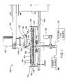
- FIG. 1depicts a schematic, partial cross-sectional side view of a processing station 100 having one embodiment of a processing pad assembly 106 of the present invention.
- the processing station 100includes a carrier head assembly 118 and a platen assembly 142 .
- the carrier head assembly 118is adapted to hold a feature side 112 of a substrate 120 against the platen assembly 142 while relative motion is provided therebetween to polish the feature side 112 of the substrate 120 .
- the relative motionmay be rotational, lateral, or some combination thereof, and is provided by at least one of the carrier head assembly 118 and the platen assembly 142 .
- the carrier head assembly 118is supported by an arm 164 coupled to a column 130 and which extends over the platen assembly 142 .
- the carrier head assembly 118generally includes a drive system 102 coupled to a carrier head 122 .
- the drive system 102generally provides at least rotational motion to the carrier head 122 .
- the carrier head 122additionally may be actuated toward the platen assembly 142 such that the substrate 120 retained in the carrier head 122 may be disposed against a processing surface 126 of the platen assembly 142 during processing.
- the carrier head 122may be a TITAN HEADTM or TITAN PROFILERTM wafer carrier manufactured by Applied Materials, Inc., of Santa Clara, Calif.
- the carrier head 122comprises a housing 124 and retaining ring 126 that define a center recess in which the substrate 120 is retained.
- the retaining ring 126circumscribes the substrate 120 disposed within the carrier head 122 , while leaving the feature side 112 exposed, to prevent the substrate from slipping out from under the carrier head 122 during processing. It is contemplated that other polishing heads may be utilized.
- the platen assembly 142is rotationally disposed on a base 158 .
- a bearing 154is disposed between the platen assembly 142 and the base 158 to facilitate rotation of the platen assembly 142 relative to the base 158 .
- a motor 160is coupled to the platen assembly 142 to provide rotational motion.
- the platen assembly 142includes an upper plate 114 and a lower plate 148 .
- the upper plate 114may be fabricated from a rigid material, such as a metal or rigid plastic, and in one embodiment, is fabricated from or coated with a dielectric material, such as chlorinated polyvinyl chloride (CPVC).
- CPVCchlorinated polyvinyl chloride
- the upper plate 114may have a circular, rectangular or other geometric form with a substantially planar top surface 116 .
- the top surface 116 of the upper plate 114supports the pad assembly 106 thereon.
- the pad assembly 106may be held to the top surface 116 of the upper plate 114 by magnetic attraction, electrostatic attraction, vacuum, adhesives, or the like.
- the lower plate 148is generally fabricated from a rigid material, such as aluminum and may be coupled to the upper plate 114 by any conventional means, such as a plurality of fasteners (not shown). Generally, a plurality of locating pins 146 (one is shown in FIG. 1 ) are disposed between the upper and lower plates 114 , 148 to ensure alignment therebetween.
- the upper plate 114 and the lower plate 148may optionally be fabricated from a single, unitary member.
- a plenum 138is defined in the platen assembly 142 and may be partially formed in at least one of the upper or lower plates 114 , 148 .
- the plenum 138is defined in a recess 144 partially formed in the lower surface of the upper plate 114 .
- At least one hole 108is formed in the upper plate 114 to allow electrolyte, provided to the plenum 138 from an electrolyte source 170 , to flow through the platen assembly 142 and into contact with the substrate 120 during processing.
- the plenum 138is partially bounded by a cover 150 coupled to the upper plate 114 enclosing the recess 144 .
- the electrolytemay be dispensed from a pipe (not shown) onto the top surface of the pad assembly 106 . It is contemplated that platen assemblies having other configurations may be utilized.
- the pad assembly 106includes at least a processing layer 104 and an electrode 110 .
- the processing layer 104has a working surface 128 that, in one embodiment, is adapted to polish the feature side 112 of the substrate 120 during processing.
- the working surface 128may be smooth or patterned to facilitate distribution of a polishing fluid or electrolyte over the surface of the pad assembly 106 . Patterns may include grooves, cutouts, perforations, and the like.
- the processing layer 104may be fabricated from polymeric materials compatible with the process chemistry, examples of which include polyurethane, polycarbonate, fluoropolymers, PTFE, PTFA, polyphenylene sulfide (PPS), or combinations thereof, and other polishing materials used in polishing substrate surfaces.
- the working surface 128 of the processing layer 104is dielectric, for example, polyurethane or other polymer.
- the working surface 128 of the processing layer 104may include conductive material or include conductive contact elements extending therefrom.
- the working surface 128may be fabricated from a conductive composite (i.e., the conductive elements are dispersed integrally with or comprise the material comprising the polishing surface), such as a polymer matrix having conductive particles dispersed therein or a conductive coated fabric, among others.
- a conductive compositei.e., the conductive elements are dispersed integrally with or comprise the material comprising the polishing surface
- the electrode 110is generally positioned between the working surface 128 of the processing layer 104 and the top surface 116 of the platen assembly 142 .
- the electrode 110can be a plate-like member or laminate, a plate having multiple apertures formed therethrough, or a plurality of electrode pieces disposed in a permeable membrane or container.
- the electrode 110may be a metal foil, a mesh made of metal wire or metal-coated wire, or a laminated metal layer on a polymer film compatible with the electrolyte, such as a polyimide, polyester, flouroethylene, polypropylene, or polyethylene sheet.
- the electrode 110may act as a single electrode, or may comprise multiple independent electrode zones isolated from each other. Zoned electrodes are discussed in U.S.
- the electrode 110is fabricated of a material compatible with electrolyte chemistries and generally has a low bulk conductivity.
- the stiffness of the electrode 110should be low enough to ensure the processing layer 104 conforms to the substrate 120 and retains a generally flat profile (i.e., does not have a “potato chip” form).
- the electrode 110is typically comprised of a corrosion resistant conductive material, such as metals, conductive alloys, metal coated fabrics, conductive polymers, conductive pads, and the like.
- Conductive metalsinclude Sn, Ni, Cu, Au, and the like.
- Conductive metalsalso include a corrosion resistant metal such as Sn, Ni, or Au coated over an active metal such as Cu, Zn, Al, and the like.
- Conductive alloysinclude inorganic alloys and metal alloys such as bronze, brass, stainless steel, or palladium-tin alloys, among others.
- Metal coated fabricmay be woven or non-woven with any corrosion resistant metal coating.
- Conductive padsconsist of conductive fillers disposed in a polymer matrix.
- the electrode 110When metal is used as material for the electrode 110 , it may be a solid sheet. Alternatively, the electrode 110 may be perforated or formed of a metal screen in order to increase surface area, which increases the substrate removal rate during processing.
- the pad assembly 106is at least partially permeable to electrolyte at least between the electrode 110 and the working surface 128 of the processing layer 104 .
- the pad assembly 106is adapted to electrically bias the substrate 120 during processing by electrically coupling the substrate 120 to one terminal of the power source 166 .
- the electrode 110 of the pad assembly 106is coupled to another terminal of the power source 166 .
- the electrolytewhich is introduced from the electrolyte source 170 and is disposed on the pad assembly 106 , completes an electrical circuit between the substrate 120 and the electrode 110 of the pad assembly 106 , which, in one embodiment, assists in the removal of material from the surface of the substrate 120 .
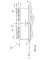
- FIG. 2Adepicts one embodiment of the pad assembly 106 .
- the pad assembly 106includes at least an electrode 110 interposed between the processing layer 104 and a subpad 212 .
- the processing layer 104is non-conductive.
- a conductive processing layercould be utilized with an intervening insulating layer 220 (shown in phantom) disposed between the processing layer 104 and the electrode 110 .
- a terminal 202is formed on the electrode 110 to facilitate connection with the power source 166 .
- the electrode 110 , subpad 212 , and processing layer 104 of the pad assembly 106may be combined into a unitary assembly by the use of adhesives, bonding, compression molding, or the like.
- adhesiveis used to attach the electrode 110 , subpad 212 , and processing layer 104 together.
- the adhesivegenerally is a pressure sensitive adhesive or a temperature sensitive adhesive and should be compatible with the process chemistry as well as with the different materials used for the electrode 110 , subpad 212 , and/or processing layer 104 .
- the adhesivemay have a strong physical and/or chemical bond to the electrode 110 , subpad 212 , and processing layer 104 . However, selection of the adhesive may also depend upon the form of the electrode 110 , subpad 212 , and processing layer 104 .
- the adhesive bonding between the electrode 110 , subpad 212 , and processing layer 104may be increased by the surface morphology of the materials selected to form the pad assembly 106 (i.e., fabrics, screens, and perforations versus solids). For example, if the electrode 110 is fabricated from a screen, mesh, or perforated foil, a weaker adhesive may be selected due to the increased surface area of the electrode 110 .
- the pad assembly 106is disposed on the top surface 116 of the upper plate 114 of the platen assembly 142 and may be held there by magnetic attraction, static attraction, vacuum, adhesives, or the like. In one embodiment, adhesive is used to adhere the subpad 212 of the pad assembly 106 to the upper plate 114 .
- At least one permeable passage 218is disposed through the processing layer 104 and extends at least to the electrode 110 .
- the passage 218allows an electrolyte to establish a conductive path through the processing layer 104 between the substrate 120 and the electrode 110 .
- the passage 218may be a permeable portion of the processing layer 104 , holes formed in the processing layer 104 , or a combination of the two.
- the permeable passage 218is a plurality of holes 216 formed in and through the processing layer 104 to allow an electrolyte to flow therethrough and come into contact with the electrode 110 during processing.
- the plurality of holes 216may be formed in a rectangular pattern, a triangular pattern, or any other uniformly distributed pattern and generally has a percent open area of from about 10% to about 90% (i.e., the area of the holes open to the electrode as a percentage of the total surface area of the polishing layer).
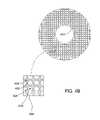
- FIG. 2Bdepicts a plan view of one embodiment of a pad assembly 106 having a plurality of holes 216 uniformly distributed across the surface of the pad assembly 106 .
- FIG. 2Cdepicts a plan view of another embodiment of a pad assembly 106 having a first plurality of holes 216 A uniformly distributed across a first zone 290 of the pad assembly 106 and a second plurality of holes 216 B uniformly distributed across a second zone 292 of the pad assembly 106 .
- the quantity and location of zones as well as the percent open area within each zonemay be selected to achieve desired processing performance of the pad assembly 106 .
- Zoned processing pad assembliesare discussed in greater detail in co-pending U.S. patent application Ser. No. 10/727,774 (titled PROCESSING PAD ASSEMBLY WITH ZONE CONTROL, filed Dec. 3, 2003 by ANTOINE P. MANENS, which is hereby incorporated by reference in its entirety.
- FIGS. 2A–2Care round, it is contemplated that any shape or form of opening which allows electrolyte to flow through the processing layer 104 and to come into contact with the electrode 110 and the substrate 120 during processing.
- the teachings described herein with respect to the at least one permeable passage 218e.g., the plurality of holes 216 , distribution, percent open area, zones, and the like, are equally applicable to all embodiments of polishing pad assemblies described herein.
- the plurality of holes 216may be molded in the processing layer 104 as formed, or the holes 216 may be formed by, for example, a steel rule die, an ultrasonic knife/punch, or a male/female die punch, among other forming methods. Care should be taken in perforating the processing layer 104 as any irregularities in the working surface 128 of the processing layer 104 may cause damage to the substrate 120 .
- the location and open area percentage of the holes 216 in the processing layer 104controls the quantity and distribution of electrolyte contacting the electrode 110 and substrate 120 during processing, thereby controlling the rate of removal of material from the surface of the substrate 120 in a polishing operation, or the rate of deposition in a plating operation.
- an extension 222 of the permeable passage 218may be formed in and at least partially through the electrode 110 (shown in phantom) in order to increase the surface area of the electrode 110 in contact with the electrolyte.
- the extension 222may extend completely through the electrode 110 .
- the larger surface area of electrolyte contact with the electrode 110improves the rate of removal of material from the surface of the substrate 120 during polishing and the rate of deposition during plating.
- the subpad 212is typically made of a material softer, or more compliant, than the material of the processing layer 104 .
- the difference in hardness or durometer between the processing layer 104 and the subpad 212may be chosen to produce a desired polishing/plating performance.
- the subpad 212may also be compressible. Examples of suitable subpad 212 materials include, but are not limited to, open or closed-cell foamed polymer, elastomers, felt, impregnated felt, plastics, and like materials compatible with the processing chemistries.
- At least one aperture 240is formed through the pad assembly 106 .
- Each of the at least one aperture 240is of a size and location to accommodate a contact element 234 passing therethrough.
- one aperture 240is centrally formed through the processing layer 104 , electrode 110 , and subpad 212 of the pad assembly 106 .
- the aperture 240is aligned with the contact element 234 centrally disposed on the upper plate 114 of the platen assembly 142 .
- the contact element 234is coupled through the platen assembly 142 to the power source 166 and is adapted to electrically bias the feature side 112 of the substrate 120 during processing. Examples of contact elements 234 suitable for use with this invention are more fully described in U.S. patent application Ser. No.
- contact element 234may be disposed on the upper plate 114 of the platen assembly 142 in any number or geometry.
- the contact element 234may be include a plurality of conductive elements disposed in or embedded within the processing layer 104 , or the processing layer 104 may be made of a conductive material, or some combination of conductive and non-conductive elements, materials, and the like.
- FIGS. 3A and 3Bdepict another embodiment of a pad assembly 306 having at least a processing layer 304 interposed between an electrode 310 and a subpad 312 .
- a terminal 302is formed on the electrode to facilitate coupling the electrode 310 to the power source 166 .
- the electrode 310is perforated by a plurality of holes 350 .
- the processing layer 304has a plurality of coincident raised portions 330 which align with and protrude through the plurality of holes 350 on the electrode 310 to form a plurality of discrete working surfaces 328 disposed above the electrode 310 .
- the recessed area between the raised portions 330facilitate the flow of electrolyte and/or polishing fluid across the electrode 310 and improve the processing rate and surface uniformity of the substrate 120 .
- the discrete working surfaces 328being decoupled from one another, promote global conformance of the discrete working surfaces 328 to the feature side 112 of the substrate 120 during processing.
- the processing layer 304is dielectric, for example, polyurethane.
- the processing layer 304could be conductive.
- an insulatormay be disposed between the processing layer 304 and the electrode 310 by, for example, coating the electrode 310 with a dielectric and selectively removing the coating where exposure of the electrode 310 to the electrolyte is desired.
- FIGS. 4A and 4Bdepict another embodiment of a pad assembly 406 having at least a processing layer 404 and an electrode 410 .
- a terminal 402is formed on the electrode 410 to facilitate coupling the electrode 410 to the power source 166 .
- the processing layer 404includes a plurality of grooves 452 formed partially through the processing layer 404 and a plurality of permeable passages 418 extending completely through the processing layer 404 .
- An insulative layer 411(shown in phantom), for example a dielectric, is disposed between the processing layer 404 and the electrode 410 when the processing layer 404 is conductive. The insulative layer 411 is permeable to electrolyte at least where electrolyte contact with the electrode is desired.
- the insulative layer 411may be perforated with holes to extend the permeable passage 418 to the electrode 410 .
- the grooves 452are arranged in a orthogonal grid. Alternatively, the grooves may be arranged in a triangular pattern, concentric circles, spirals, waves, or a combination thereof, among other configurations.
- the grooves 452facilitate the flow of electrolyte and/or polishing fluid across the processing layer 404 and improve the processing rate and surface uniformity of the substrate 120 by ensuring good electrical contact to a large surface area of the electrode 410 .
- the pattern of the grooves 452forms a plurality of discrete pad areas 454 in the processing layer 404 .
- the discrete pad areas 454have more flexibility to conform to the feature side 112 of the substrate 120 during processing.
- the permeable passages 418allow electrolyte to contact the electrode 410 and the substrate 120 during processing.
- the plurality of permeable passages 418is a plurality of holes 450 extending completely through the processing layer 404 .
- the holes 450may be formed within the grooves 452 such that any protrusions, burrs, flash, or unevenness which may be caused by the forming of the holes 450 in the processing layer 404 is disposed below a working surface 428 of the pad assembly 406 .
- the plurality of holes 450have a diameter which is larger than the nominal width of the grooves 452 , and the grooves 452 are widened at each intersection in order to circumscribe each of the holes 450 .
- the spacing of the permeable passages 418 below the working surface 428advantageously reduces the probability of damage to the feature side 112 of the substrate 120 from any anomalies around the edges of the permeable passages 418 .
- processing pad assemblies discussed aboveare general depictions of the configuration of the processing layer and the electrode and any other necessary components, as noted. It is contemplated that other layers may be added and/or configurations may be construed using the principles discussed above. For example, release layers and liners may be added to accommodate the attachment and detachment of the polishing pad assemblies from the platen assembly.
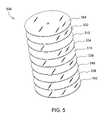
- FIG. 5depicts an exemplary illustration of one embodiment of a pad assembly 506 configured to facilitate handling and replacement.
- a processing layer 504 and electrode 510are interposed by a subpad 512 .
- the processing layer 504 , electrode 510 , and subpad 512are bonded together by adhesive layers 532 , 534 .
- An adhesive layer 536bonds a release film 540 to the bottom of the electrode 510 .
- a final adhesive layer 538is disposed below the release film 540 to facilitate adhering to the upper plate 114 of the platen assembly 142 (shown in FIG. 1 ).
- a liner 542is attached to the final adhesive layer 538 to facilitate handling and is removed prior to installation.
- the release filmfacilitates easy removal of the pad assembly 506 from the platen assembly 142 .
- the release film, liner, and intervening adhesive layersmay be utilized in other embodiments of the pad assembly, including those embodiments described above.
Landscapes
- Engineering & Computer Science (AREA)
- Mechanical Engineering (AREA)
- Chemical & Material Sciences (AREA)
- Chemical Kinetics & Catalysis (AREA)
- Electrochemistry (AREA)
- Manufacturing & Machinery (AREA)
- Condensed Matter Physics & Semiconductors (AREA)
- General Physics & Mathematics (AREA)
- Physics & Mathematics (AREA)
- Computer Hardware Design (AREA)
- Microelectronics & Electronic Packaging (AREA)
- Power Engineering (AREA)
- Materials Engineering (AREA)
- Metallurgy (AREA)
- Organic Chemistry (AREA)
- Mechanical Treatment Of Semiconductor (AREA)
- Finish Polishing, Edge Sharpening, And Grinding By Specific Grinding Devices (AREA)
Abstract
Description
This application is a continuation-in-part of U.S. patent application Ser. No. 10/642,128, filed Aug. 15, 2003 Now U.S. Pat. No. 6,962,524 (hereinafter the '128 application). The '128 application is a continuation-in-part of co-pending U.S. patent application Ser. No. 10/608,513, filed Jun. 26, 2003 (hereinafter referred to as the “'513 application”), which is a continuation-in-part of U.S. patent application Ser. No. 10/140,010, filed May 7, 2002 Now U.S. Pat. No. 6,979,248. The '513 application is also a continuation-in-part of co-pending U.S. patent application Ser. No. 10/211,626, filed Aug. 2, 2002, which is a continuation-in-part of co-pending U.S. patent application Ser. No. 10/033,732, filed Dec. 27, 2001, which is a continuation-in-part of U.S. patent application Ser. No. 09/505,899, filed Feb. 17, 2000 Now U.S. Pat. No. 6,537,144. The '513 application is additionally a continuation-in-part of co-pending U.S. patent application Ser. No. 10/210,972, filed Aug. 2, 2002; which is also a continuation-in-part of U.S. patent application Ser. No. 09/505,899, filed Feb. 17, 2000 Now U.S. Pat. No. 6,537,144. The '513 application is further a continuation-in-part of U.S. patent application Ser. No. 10/151,538, filed May 16, 2002 Now abandoned. The '128 application is also a continuation-in-part of co-pending U.S. patent application Ser. No. 10/244,697, filed Sep. 16, 2002, which is a continuation-in-part of U.S. application Ser. No. 10/244,688, filed Sep. 16, 2002 Now U.S. Pat. No. 6,848,970, and of co-pending U.S. patent application Ser. No. 10/391,324, filed Mar. 18, 2003. All of the above referenced applications are hereby incorporated by reference in their entireties.
This application is additionally related to U.S. patent application Ser. No. 10/033,732, filed on Dec. 27, 2001; U.S. patent application Ser. No. 10/455,941, filed Jun. 6, 2003; and U.S. patent application Ser. No. 10/455,895, filed Jun. 6, 2003, all of which are also incorporated herein by reference in their entireties.
1. Field of the Invention
Embodiments of the present invention generally relate to a pad assembly for electrochemical mechanical processing.
2. Description of the Related Art
Electrochemical Mechanical Processing (ECMP) is a technique used to remove conductive materials from a substrate surface by electrochemical dissolution while concurrently polishing the substrate with reduced mechanical abrasion as compared to conventional Chemical Mechanical Polishing (CMP) processes. ECMP systems may generally be adapted for deposition of conductive material on the substrate by reversing the polarity of the bias. Electrochemical dissolution is performed by applying a bias between a cathode and a substrate surface to remove conductive materials from the substrate surface into a surrounding electrolyte. The bias may be applied to the substrate surface by a conductive contact disposed on or through a polishing material upon which the substrate is processed. A mechanical component of the polishing process is performed by providing relative motion between the substrate and the polishing material that enhances the removal of the conductive material from the substrate.
Copper is one material that may be polished using electrochemical mechanical polishing. Typically, copper is polished utilizing a two-step process. In the first step, the bulk of the copper is removed, typically leaving some copper residue on the substrate's surface. The copper residue is then removed in a second, or over-polishing, step.
During electrochemical processing, the copper layer disposed on the substrate is pressed against a polishing surface and is biased relative to an electrode. An electrolyte fluid is disposed between the copper layer and the electrode. The electrolyte completes an electrical circuit between the substrate and the electrode, which assists in the removal of material from the surface of the substrate. As the polishing surface and electrode are consumed during processing a number of substrates, periodic replacement of both the polishing surface and electrode is required, thus necessitating interruption of substrate processing. Therefore, it is desirable to configure the polishing surface, electrode and polishing system in general in a configuration that facilitates quick and efficient replacement of the polishing surface and electrode to minimize process interruptions.
Thus, there is a need for an improved apparatus for electrochemical mechanical processing.
In one embodiment, a pad assembly for processing a substrate are provided. The pad assembly includes a processing layer having a working surface adapted to process a substrate, a lower layer coupled to and disposed below the processing layer, and an electrode having an upper surface disposed above the lower layer and below the working surface of the processing layer. The upper surface of the electrode is at least partially exposed to the working surface to provide an electrolyte pathway between the upper surface of the electrode and the working surface.
So that the manner in which the above recited features, advantages and objects of the present invention are attained and can be understood in detail, a more particular description of the invention, briefly summarized above, may be had by reference to the embodiments thereof which are illustrated in the appended drawings. It is to be noted, however, that the appended drawings illustrate only typical embodiments of this invention and are therefore not to be considered limiting of its scope, for the invention may admit to other equally effective embodiments.
To facilitate understanding, identical reference numerals have been used, where possible, to designate identical elements that are common to the figures.
A processing pad assembly adapted to enhance uniform deposition/removal of material to/from a substrate is provided herein. The processing pad assembly is additionally configured to facilitate efficient removal and replacement, thereby improving system processing capacity. The processing pad assembly includes at least a processing pad having a working surface and an electrode. The processing pad is at least partially permeable to electrolyte and is adapted to allow biasing of a feature side of a substrate during processing. Although the embodiments disclosed below focus primarily on polishing a substrate, it is contemplated that the teachings disclosed herein may be used to electroplate a substrate by reversing the polarity of the bias.
In one embodiment, thecarrier head assembly 118 is supported by anarm 164 coupled to acolumn 130 and which extends over theplaten assembly 142. Thecarrier head assembly 118 generally includes adrive system 102 coupled to acarrier head 122. Thedrive system 102 generally provides at least rotational motion to thecarrier head 122. Thecarrier head 122 additionally may be actuated toward theplaten assembly 142 such that thesubstrate 120 retained in thecarrier head 122 may be disposed against aprocessing surface 126 of theplaten assembly 142 during processing.
In one embodiment, thecarrier head 122 may be a TITAN HEAD™ or TITAN PROFILER™ wafer carrier manufactured by Applied Materials, Inc., of Santa Clara, Calif. Generally, thecarrier head 122 comprises ahousing 124 and retainingring 126 that define a center recess in which thesubstrate 120 is retained. The retainingring 126 circumscribes thesubstrate 120 disposed within thecarrier head 122, while leaving thefeature side 112 exposed, to prevent the substrate from slipping out from under thecarrier head 122 during processing. It is contemplated that other polishing heads may be utilized.
Theplaten assembly 142 is rotationally disposed on abase 158. Abearing 154 is disposed between theplaten assembly 142 and the base158 to facilitate rotation of theplaten assembly 142 relative to thebase 158. Amotor 160 is coupled to theplaten assembly 142 to provide rotational motion.
In one embodiment, theplaten assembly 142 includes anupper plate 114 and alower plate 148. Theupper plate 114 may be fabricated from a rigid material, such as a metal or rigid plastic, and in one embodiment, is fabricated from or coated with a dielectric material, such as chlorinated polyvinyl chloride (CPVC). Theupper plate 114 may have a circular, rectangular or other geometric form with a substantially planartop surface 116. Thetop surface 116 of theupper plate 114 supports thepad assembly 106 thereon. Thepad assembly 106 may be held to thetop surface 116 of theupper plate 114 by magnetic attraction, electrostatic attraction, vacuum, adhesives, or the like.
Thelower plate 148 is generally fabricated from a rigid material, such as aluminum and may be coupled to theupper plate 114 by any conventional means, such as a plurality of fasteners (not shown). Generally, a plurality of locating pins146 (one is shown inFIG. 1 ) are disposed between the upper andlower plates upper plate 114 and thelower plate 148 may optionally be fabricated from a single, unitary member.
Aplenum 138 is defined in theplaten assembly 142 and may be partially formed in at least one of the upper orlower plates FIG. 1 , theplenum 138 is defined in arecess 144 partially formed in the lower surface of theupper plate 114. At least onehole 108 is formed in theupper plate 114 to allow electrolyte, provided to theplenum 138 from anelectrolyte source 170, to flow through theplaten assembly 142 and into contact with thesubstrate 120 during processing. Theplenum 138 is partially bounded by acover 150 coupled to theupper plate 114 enclosing therecess 144. Alternatively, the electrolyte may be dispensed from a pipe (not shown) onto the top surface of thepad assembly 106. It is contemplated that platen assemblies having other configurations may be utilized.
Thepad assembly 106 includes at least aprocessing layer 104 and anelectrode 110. Theprocessing layer 104 has a workingsurface 128 that, in one embodiment, is adapted to polish thefeature side 112 of thesubstrate 120 during processing. The workingsurface 128 may be smooth or patterned to facilitate distribution of a polishing fluid or electrolyte over the surface of thepad assembly 106. Patterns may include grooves, cutouts, perforations, and the like. Theprocessing layer 104 may be fabricated from polymeric materials compatible with the process chemistry, examples of which include polyurethane, polycarbonate, fluoropolymers, PTFE, PTFA, polyphenylene sulfide (PPS), or combinations thereof, and other polishing materials used in polishing substrate surfaces. In one embodiment, the workingsurface 128 of theprocessing layer 104 is dielectric, for example, polyurethane or other polymer.
In another embodiment, the workingsurface 128 of theprocessing layer 104 may include conductive material or include conductive contact elements extending therefrom. For example, the workingsurface 128 may be fabricated from a conductive composite (i.e., the conductive elements are dispersed integrally with or comprise the material comprising the polishing surface), such as a polymer matrix having conductive particles dispersed therein or a conductive coated fabric, among others. Examples of processing layers that may be adapted to benefit from the invention are described in U.S. patent application Ser. No. 10/455,941, filed Jun. 6, 2003 by Y. Hu et al. (entitled “CONDUCTIVE POLISHING ARTICLE FOR ELECTROCHEMICAL MECHANICAL POLISHING”) and U.S. patent application Ser. No. 10/455,895, filed Jun. 6, 2003 by Y. Hu et al. (entitled “CONDUCTIVE POLISHING ARTICLE FOR ELECTROCHEMICAL MECHANICAL POLISHING”), both of which are hereby incorporated by reference in their entireties.
Theelectrode 110 is generally positioned between the workingsurface 128 of theprocessing layer 104 and thetop surface 116 of theplaten assembly 142. Theelectrode 110 can be a plate-like member or laminate, a plate having multiple apertures formed therethrough, or a plurality of electrode pieces disposed in a permeable membrane or container. For example, theelectrode 110 may be a metal foil, a mesh made of metal wire or metal-coated wire, or a laminated metal layer on a polymer film compatible with the electrolyte, such as a polyimide, polyester, flouroethylene, polypropylene, or polyethylene sheet. Theelectrode 110 may act as a single electrode, or may comprise multiple independent electrode zones isolated from each other. Zoned electrodes are discussed in U.S. patent application Ser. No. 10/642,128, filed Aug. 15, 2003, which is hereby incorporated by reference in its entirety.
Theelectrode 110 is fabricated of a material compatible with electrolyte chemistries and generally has a low bulk conductivity. The stiffness of theelectrode 110 should be low enough to ensure theprocessing layer 104 conforms to thesubstrate 120 and retains a generally flat profile (i.e., does not have a “potato chip” form).
Theelectrode 110 is typically comprised of a corrosion resistant conductive material, such as metals, conductive alloys, metal coated fabrics, conductive polymers, conductive pads, and the like. Conductive metals include Sn, Ni, Cu, Au, and the like. Conductive metals also include a corrosion resistant metal such as Sn, Ni, or Au coated over an active metal such as Cu, Zn, Al, and the like. Conductive alloys include inorganic alloys and metal alloys such as bronze, brass, stainless steel, or palladium-tin alloys, among others. Metal coated fabric may be woven or non-woven with any corrosion resistant metal coating. Conductive pads consist of conductive fillers disposed in a polymer matrix.
When metal is used as material for theelectrode 110, it may be a solid sheet. Alternatively, theelectrode 110 may be perforated or formed of a metal screen in order to increase surface area, which increases the substrate removal rate during processing.
Thepad assembly 106 is at least partially permeable to electrolyte at least between theelectrode 110 and the workingsurface 128 of theprocessing layer 104. Thepad assembly 106 is adapted to electrically bias thesubstrate 120 during processing by electrically coupling thesubstrate 120 to one terminal of thepower source 166. Theelectrode 110 of thepad assembly 106 is coupled to another terminal of thepower source 166. The electrolyte, which is introduced from theelectrolyte source 170 and is disposed on thepad assembly 106, completes an electrical circuit between thesubstrate 120 and theelectrode 110 of thepad assembly 106, which, in one embodiment, assists in the removal of material from the surface of thesubstrate 120.
Theelectrode 110,subpad 212, andprocessing layer 104 of thepad assembly 106 may be combined into a unitary assembly by the use of adhesives, bonding, compression molding, or the like. In one embodiment, adhesive is used to attach theelectrode 110,subpad 212, andprocessing layer 104 together. The adhesive generally is a pressure sensitive adhesive or a temperature sensitive adhesive and should be compatible with the process chemistry as well as with the different materials used for theelectrode 110,subpad 212, and/orprocessing layer 104. The adhesive may have a strong physical and/or chemical bond to theelectrode 110,subpad 212, andprocessing layer 104. However, selection of the adhesive may also depend upon the form of theelectrode 110,subpad 212, andprocessing layer 104. The adhesive bonding between theelectrode 110,subpad 212, andprocessing layer 104 may be increased by the surface morphology of the materials selected to form the pad assembly106 (i.e., fabrics, screens, and perforations versus solids). For example, if theelectrode 110 is fabricated from a screen, mesh, or perforated foil, a weaker adhesive may be selected due to the increased surface area of theelectrode 110.
Thepad assembly 106 is disposed on thetop surface 116 of theupper plate 114 of theplaten assembly 142 and may be held there by magnetic attraction, static attraction, vacuum, adhesives, or the like. In one embodiment, adhesive is used to adhere thesubpad 212 of thepad assembly 106 to theupper plate 114.
In one embodiment, at least onepermeable passage 218 is disposed through theprocessing layer 104 and extends at least to theelectrode 110. Thepassage 218 allows an electrolyte to establish a conductive path through theprocessing layer 104 between thesubstrate 120 and theelectrode 110. Thepassage 218 may be a permeable portion of theprocessing layer 104, holes formed in theprocessing layer 104, or a combination of the two. In the embodiment depicted inFIG. 2A , thepermeable passage 218 is a plurality ofholes 216 formed in and through theprocessing layer 104 to allow an electrolyte to flow therethrough and come into contact with theelectrode 110 during processing. The plurality ofholes 216 may be formed in a rectangular pattern, a triangular pattern, or any other uniformly distributed pattern and generally has a percent open area of from about 10% to about 90% (i.e., the area of the holes open to the electrode as a percentage of the total surface area of the polishing layer). For example,FIG. 2B depicts a plan view of one embodiment of apad assembly 106 having a plurality ofholes 216 uniformly distributed across the surface of thepad assembly 106.
Although the pattern of theholes 216 should be uniform, theholes 216 may be grouped into different regions, or zones, of varying open area percentage with a uniform pattern within each respective zone. For example,FIG. 2C depicts a plan view of another embodiment of apad assembly 106 having a first plurality ofholes 216A uniformly distributed across afirst zone 290 of thepad assembly 106 and a second plurality ofholes 216B uniformly distributed across asecond zone 292 of thepad assembly 106. The quantity and location of zones as well as the percent open area within each zone may be selected to achieve desired processing performance of thepad assembly 106. Zoned processing pad assemblies are discussed in greater detail in co-pending U.S. patent application Ser. No. 10/727,774 (titled PROCESSING PAD ASSEMBLY WITH ZONE CONTROL, filed Dec. 3, 2003 by ANTOINE P. MANENS, which is hereby incorporated by reference in its entirety.
It should be noted that although the holes depicted inFIGS. 2A–2C are round, it is contemplated that any shape or form of opening which allows electrolyte to flow through theprocessing layer 104 and to come into contact with theelectrode 110 and thesubstrate 120 during processing. Furthermore, the teachings described herein with respect to the at least onepermeable passage 218, e.g., the plurality ofholes 216, distribution, percent open area, zones, and the like, are equally applicable to all embodiments of polishing pad assemblies described herein.
The plurality ofholes 216 may be molded in theprocessing layer 104 as formed, or theholes 216 may be formed by, for example, a steel rule die, an ultrasonic knife/punch, or a male/female die punch, among other forming methods. Care should be taken in perforating theprocessing layer 104 as any irregularities in the workingsurface 128 of theprocessing layer 104 may cause damage to thesubstrate 120. The location and open area percentage of theholes 216 in theprocessing layer 104 controls the quantity and distribution of electrolyte contacting theelectrode 110 andsubstrate 120 during processing, thereby controlling the rate of removal of material from the surface of thesubstrate 120 in a polishing operation, or the rate of deposition in a plating operation.
Optionally, anextension 222 of thepermeable passage 218 may be formed in and at least partially through the electrode110 (shown in phantom) in order to increase the surface area of theelectrode 110 in contact with the electrolyte. Theextension 222 may extend completely through theelectrode 110. The larger surface area of electrolyte contact with theelectrode 110 improves the rate of removal of material from the surface of thesubstrate 120 during polishing and the rate of deposition during plating.
Thesubpad 212 is typically made of a material softer, or more compliant, than the material of theprocessing layer 104. The difference in hardness or durometer between theprocessing layer 104 and thesubpad 212 may be chosen to produce a desired polishing/plating performance. Thesubpad 212 may also be compressible. Examples ofsuitable subpad 212 materials include, but are not limited to, open or closed-cell foamed polymer, elastomers, felt, impregnated felt, plastics, and like materials compatible with the processing chemistries.
At least oneaperture 240 is formed through thepad assembly 106. Each of the at least oneaperture 240 is of a size and location to accommodate acontact element 234 passing therethrough. In the embodiment depicted inFIG. 2 , oneaperture 240 is centrally formed through theprocessing layer 104,electrode 110, and subpad212 of thepad assembly 106. Theaperture 240 is aligned with thecontact element 234 centrally disposed on theupper plate 114 of theplaten assembly 142. Thecontact element 234 is coupled through theplaten assembly 142 to thepower source 166 and is adapted to electrically bias thefeature side 112 of thesubstrate 120 during processing. Examples ofcontact elements 234 suitable for use with this invention are more fully described in U.S. patent application Ser. No. 10/642,128 filed Aug. 15, 2003, previously incorporated by reference in its entirety. Although only onecontact element 234 is depicted inFIG. 2A ,multiple contact elements 234 may be disposed on theupper plate 114 of theplaten assembly 142 in any number or geometry. Alternatively, thecontact element 234 may be include a plurality of conductive elements disposed in or embedded within theprocessing layer 104, or theprocessing layer 104 may be made of a conductive material, or some combination of conductive and non-conductive elements, materials, and the like.
In the embodiment depicted inFIGS. 3A and 3B , theprocessing layer 304 is dielectric, for example, polyurethane. Alternatively, theprocessing layer 304 could be conductive. In embodiments where theprocessing layer 304 is conductive, an insulator may be disposed between theprocessing layer 304 and theelectrode 310 by, for example, coating theelectrode 310 with a dielectric and selectively removing the coating where exposure of theelectrode 310 to the electrolyte is desired.
Thepermeable passages 418 allow electrolyte to contact theelectrode 410 and thesubstrate 120 during processing. In the embodiment depicted inFIGS. 4A and 4B , the plurality ofpermeable passages 418 is a plurality ofholes 450 extending completely through theprocessing layer 404. Theholes 450 may be formed within thegrooves 452 such that any protrusions, burrs, flash, or unevenness which may be caused by the forming of theholes 450 in theprocessing layer 404 is disposed below a workingsurface 428 of thepad assembly 406. In the embodiment depicted inFIGS. 4A and 4B , the plurality ofholes 450 have a diameter which is larger than the nominal width of thegrooves 452, and thegrooves 452 are widened at each intersection in order to circumscribe each of theholes 450. The spacing of thepermeable passages 418 below the workingsurface 428 advantageously reduces the probability of damage to thefeature side 112 of thesubstrate 120 from any anomalies around the edges of thepermeable passages 418.
The embodiments of processing pad assemblies discussed above are general depictions of the configuration of the processing layer and the electrode and any other necessary components, as noted. It is contemplated that other layers may be added and/or configurations may be construed using the principles discussed above. For example, release layers and liners may be added to accommodate the attachment and detachment of the polishing pad assemblies from the platen assembly.
For example,FIG. 5 depicts an exemplary illustration of one embodiment of apad assembly 506 configured to facilitate handling and replacement. In this embodiment, aprocessing layer 504 andelectrode 510 are interposed by asubpad 512. Theprocessing layer 504,electrode 510, andsubpad 512 are bonded together byadhesive layers adhesive layer 536 bonds arelease film 540 to the bottom of theelectrode 510. Afinal adhesive layer 538 is disposed below therelease film 540 to facilitate adhering to theupper plate 114 of the platen assembly142 (shown inFIG. 1 ). Aliner 542 is attached to the finaladhesive layer 538 to facilitate handling and is removed prior to installation. The release film facilitates easy removal of thepad assembly 506 from theplaten assembly 142. The release film, liner, and intervening adhesive layers may be utilized in other embodiments of the pad assembly, including those embodiments described above.
While the foregoing is directed to the illustrative embodiment of the present invention, other and further embodiments of the invention may be devised without departing from the basic scope thereof, and the scope thereof is determined by the claims that follow.
Claims (31)
1. A pad assembly for processing a substrate, comprising:
a processing layer made of a conductive material having a working surface adapted to process the substrate;
a lower layer coupled to and disposed below the processing layer;
an electrode having an upper surface disposed above the lower layer and below the working surface of the processing layer, wherein the upper surface of the electrode is at least partially exposed to the working surface to provide an electrolyte pathway between the upper surface of the electrode and the working surface; and
an insulative layer coupled between the electrode and the processing layer.
2. The pad assembly ofclaim 1 , further comprising:
at least one aperture formed through the lower layer, the processing layer, and the electrode.
3. The pad assembly ofclaim 2 , wherein the at least one aperture is a single aperture formed through the center of the lower layer, the processing layer, and the electrode.
4. The pad assembly ofclaim 1 , wherein the working surface of the processing layer is exposed to the upper surface of the electrode through a plurality of holes formed through the processing layer.
5. The pad assembly ofclaim 4 , wherein the plurality of holes is formed in a rectangular pattern.
6. The pad assembly ofclaim 4 , wherein the plurality of holes is formed in a triangular pattern.
7. The pad assembly ofclaim 4 , whereIn the plurality of holes defines an open area of between about 10 to about 90 percent of the working surface.
8. The pad assembly ofclaim 4 , wherein the plurality of holes further comprises:
at least two concentric groupings of holes each having an open area of between about 10 to about 90 percent of the working surface, wherein at least two of the at least two groupings of holes have different size open areas.
9. The pad assembly ofclaim 1 , wherein the lower layer, electrode, and processing layer are coupled together by an adhesive.
10. The pad assembly ofclaim 9 , further comprising:
an adhesive layer formed on a bottom of the lower layer; and
a removeable liner covering the adhesive layer.
11. The pad assembly ofclaim 1 , wherein the electrode is made of one of Cu, Ti, Sn, Ni, or stainless steel.
12. The pad assembly ofclaim 1 , wherein the electrode has a stiffness low enough to ensure confomiability and remain substantially flat.
13. The pad assembly ofclaim 1 , wherein the electrode is made of a metal foil.
14. The pad assembly ofclaim 1 , wherein the electrode is made of a mesh comprised of metal wire or metal-coated wire.
15. A pad assembly for processing a substrate, comprising:
a processing layer having a working surface adapted to process the substrate;
a lower layer coupled to and disposed below the processing layer;
an electrode having an upper surface disposed above the lower layer and below the working surface of the processing layer, wherein the upper surface of the electrode is at least partially exposed to the working surface to provide an electrolyte pathway between the upper surface of the electrode and the working surface;
an insulative layer coupled between the electrode and the processing layer, wherein the processing layer is made of a conductive material;
wherein the lower layer, electrode, and processing layer are coupled together by an adhesive; and
a release film coupled to a bottom of the lower layer.
16. A pad assembly for processing a substrate, comprising:
a processing layer having a working surface adapted to process the substrate;
a lower layer coupled to and disposed below the processing layer;
an electrode having an upper surface disposed above the lower layer and below the working surface of the processing layer, wherein the upper surface of the electrode is at least partially exposed to the working surface to provide an electrolyte pathway between the upper surface of the electrode and the working surface;
an insulative layer coupled between the electrode and the processing layer, wherein the processing layer is made of a conductive material; and
wherein the electrode is made of a laminate of a metal foil on top of a polyimide, polyester, flouroethylene, polypropylene, or polyethylene film.
17. A pad assembly for processing a substrate, comprising:
a processing layer having a working surface adapted to process the substrate;
a lower layer coupled to and disposed below the processing layer;
an electrode having an upper surface disposed above the lower layer and below the working surface of the processing layer, wherein the upper surface of the electrode is at least partially exposed to the working surface to provide an electrolyte pathway between the upper surface of the electrode and the working surface;
an insulative layer coupled between the electrode and the processing layer, wherein the processing layer is made of a conductive material; and
wherein the electrode further comprises a plurality of holes formed therethrough and wherein the working surface of the processing layer protrudes through the plurality of holes and extends above the upper surface of the electrode.
18. The pad assembly ofclaim 17 , wherein the plurality of holes further comprises:
at least two concentric groupings of holes each having an open area of between about 10 to about 90 percent of the working surface, wherein at least two of the at least two groupings of holes have different size open areas.
19. The pad assembly ofclaim 17 , further comprising:
at least one aperture formed Through the lower layer, the processing layer, and the electrode.
20. The pad assembly ofclaim 19 , wherein the at least one aperture is a single aperture formed through the center of the lower layer, the processing layer, and the electrode.
21. The pad assembly ofclaim 17 , further comprising:
a dielectric layer disposed between the electrode and the processing layer, wherein the processing layer is made of a conductive material.
22. A pad assembly for processing a substrate, comprising:
an upper layer having a working surface and a lower surface;
an electrode coupled to the lower surface of the upper layer;
two or more sets of parallel grooves formed in the working surface of the upper layer;
a plurality of holes formed through the upper layer within the two or more sets of parallel grooves and extending to the lower surface; and wherein the plurality of holes further comprises:
at least two concentric groupings of holes each having an open area of between about 10 to about 90 percent of the working surface, wherein at least two of the at least two groupings of holes have different size open areas.
23. The pad assembly ofclaim 22 , further comprising:
at least one aperture formed through the upper layer and the conductive layer.
24. The pad assembly ofclaim 23 , wherein the at least one aperture is a single aperture formed through the center of the upper layer and the electrode.
25. The pad assembly ofclaim 22 , wherein the two or more sets of parallel grooves are two sets of parallel grooves orthogonally arranged to form a grid.
26. The pad assembly ofclaim 22 , wherein the two or more sets of parallel grooves are three sets of parallel grooves and wherein each set of parallel grooves is rotated with respect to the other sets of parallel grooves to form a triangular pattern.
27. The pad assembly ofclaim 22 , wherein the plurality of holes in the upper layer are further located at intersections of the grooves.
28. A pad assembly for processing a substrate, comprising:
an upper layer having a working surface and a lower surface;
an electrode coupled to the lower surface of the upper layer;
at least one groove formed in the working surface of the upper layer;
a plurality of holes formed through the upper layer within the at least one groove and extending to the lower surface; and
an insulative layer coupled between the electrode and the upper layer, wherein the upper layer is made of a conductive material.
29. A system for electro-mechanical processing a substrate, comprising:
a platen;
a carrier head adapted to retain the substrate during processing;
a lower layer disposed on the platen;
a processing layer, made of a conductive material disposed on the lower layer and having a working surface adapted to process the substrate;
an electrode having an upper surface disposed above the lower layer and below the working surface of the processing layer, wherein the upper surface of the electrode is at least partially exposed to the working surface to provide an electrolyte pathway between the upper surface of the electrode and the working surface; and
a dielectric leyer disposed between the electrode and the processing layer.
30. The system ofclaim 29 , wherein the electrode further comprises:
a plurality of holes formed therethrough and wherein the working surface of the processing layer protrudes through the plurality of holes and extends above the upper surface of the electrode.
31. The system ofclaim 29 , further comprising:
at least one groove formed in the working surface of the processing layer; and
a plurality of holes formed through the upper layer within the at least one groove and extending at least to the upper surface of the electrode.
Priority Applications (5)
| Application Number | Priority Date | Filing Date | Title |
|---|---|---|---|
| US10/744,904US7029365B2 (en) | 2000-02-17 | 2003-12-23 | Pad assembly for electrochemical mechanical processing |
| US10/980,888US20050092621A1 (en) | 2000-02-17 | 2004-11-03 | Composite pad assembly for electrochemical mechanical processing (ECMP) |
| US11/066,599US20050194681A1 (en) | 2002-05-07 | 2005-02-25 | Conductive pad with high abrasion |
| US11/369,065US7137868B2 (en) | 2000-02-17 | 2006-03-06 | Pad assembly for electrochemical mechanical processing |
| US11/562,320US7285036B2 (en) | 2000-02-17 | 2006-11-21 | Pad assembly for electrochemical mechanical polishing |
Applications Claiming Priority (12)
| Application Number | Priority Date | Filing Date | Title |
|---|---|---|---|
| US09/505,899US6537144B1 (en) | 2000-02-17 | 2000-02-17 | Method and apparatus for enhanced CMP using metals having reductive properties |
| US10/033,732US7066800B2 (en) | 2000-02-17 | 2001-12-27 | Conductive polishing article for electrochemical mechanical polishing |
| US10/140,010US6979248B2 (en) | 2002-05-07 | 2002-05-07 | Conductive polishing article for electrochemical mechanical polishing |
| US10/151,538US20030213703A1 (en) | 2002-05-16 | 2002-05-16 | Method and apparatus for substrate polishing |
| US10/210,972US7303662B2 (en) | 2000-02-17 | 2002-08-02 | Contacts for electrochemical processing |
| US10/211,626US7125477B2 (en) | 2000-02-17 | 2002-08-02 | Contacts for electrochemical processing |
| US10/244,697US6991526B2 (en) | 2002-09-16 | 2002-09-16 | Control of removal profile in electrochemically assisted CMP |
| US10/244,688US6848970B2 (en) | 2002-09-16 | 2002-09-16 | Process control in electrochemically assisted planarization |
| US10/391,324US20040182721A1 (en) | 2003-03-18 | 2003-03-18 | Process control in electro-chemical mechanical polishing |
| US10/608,513US7374644B2 (en) | 2000-02-17 | 2003-06-26 | Conductive polishing article for electrochemical mechanical polishing |
| US10/642,128US6962524B2 (en) | 2000-02-17 | 2003-08-15 | Conductive polishing article for electrochemical mechanical polishing |
| US10/744,904US7029365B2 (en) | 2000-02-17 | 2003-12-23 | Pad assembly for electrochemical mechanical processing |
Related Parent Applications (1)
| Application Number | Title | Priority Date | Filing Date |
|---|---|---|---|
| US10/642,128Continuation-In-PartUS6962524B2 (en) | 2000-02-17 | 2003-08-15 | Conductive polishing article for electrochemical mechanical polishing |
Related Child Applications (3)
| Application Number | Title | Priority Date | Filing Date |
|---|---|---|---|
| US10/980,888Continuation-In-PartUS20050092621A1 (en) | 2000-02-17 | 2004-11-03 | Composite pad assembly for electrochemical mechanical processing (ECMP) |
| US11/066,599Continuation-In-PartUS20050194681A1 (en) | 2002-05-07 | 2005-02-25 | Conductive pad with high abrasion |
| US11/369,065ContinuationUS7137868B2 (en) | 2000-02-17 | 2006-03-06 | Pad assembly for electrochemical mechanical processing |
Publications (2)
| Publication Number | Publication Date |
|---|---|
| US20040163946A1 US20040163946A1 (en) | 2004-08-26 |
| US7029365B2true US7029365B2 (en) | 2006-04-18 |
Family
ID=36773510
Family Applications (3)
| Application Number | Title | Priority Date | Filing Date |
|---|---|---|---|
| US10/744,904Expired - Fee RelatedUS7029365B2 (en) | 2000-02-17 | 2003-12-23 | Pad assembly for electrochemical mechanical processing |
| US11/369,065Expired - Fee RelatedUS7137868B2 (en) | 2000-02-17 | 2006-03-06 | Pad assembly for electrochemical mechanical processing |
| US11/562,320Expired - Fee RelatedUS7285036B2 (en) | 2000-02-17 | 2006-11-21 | Pad assembly for electrochemical mechanical polishing |
Family Applications After (2)
| Application Number | Title | Priority Date | Filing Date |
|---|---|---|---|
| US11/369,065Expired - Fee RelatedUS7137868B2 (en) | 2000-02-17 | 2006-03-06 | Pad assembly for electrochemical mechanical processing |
| US11/562,320Expired - Fee RelatedUS7285036B2 (en) | 2000-02-17 | 2006-11-21 | Pad assembly for electrochemical mechanical polishing |
Country Status (1)
| Country | Link |
|---|---|
| US (3) | US7029365B2 (en) |
Cited By (16)
| Publication number | Priority date | Publication date | Assignee | Title |
|---|---|---|---|---|
| US20060148381A1 (en)* | 2000-02-17 | 2006-07-06 | Applied Materials, Inc. | Pad assembly for electrochemical mechanical processing |
| US20060172671A1 (en)* | 2001-04-24 | 2006-08-03 | Applied Materials, Inc. | Conductive polishing article for electrochemical mechanical polishing |
| US20070099552A1 (en)* | 2001-04-24 | 2007-05-03 | Applied Materials, Inc. | Conductive pad with ion exchange membrane for electrochemical mechanical polishing |
| US20070151867A1 (en)* | 2006-01-05 | 2007-07-05 | Applied Materials, Inc. | Apparatus and a method for electrochemical mechanical processing with fluid flow assist elements |
| US20070218587A1 (en)* | 2006-03-07 | 2007-09-20 | Applied Materials, Inc. | Soft conductive polymer processing pad and method for fabricating the same |
| US20070235344A1 (en)* | 2006-04-06 | 2007-10-11 | Applied Materials, Inc. | Process for high copper removal rate with good planarization and surface finish |
| US20070251832A1 (en)* | 2006-04-27 | 2007-11-01 | Applied Materials, Inc. | Method and apparatus for electrochemical mechanical polishing of cu with higher liner velocity for better surface finish and higher removal rate during clearance |
| US20070287361A1 (en)* | 2006-06-13 | 2007-12-13 | Brian Bottema | Method of polishing a layer using a polishing pad |
| US20080192448A1 (en)* | 2005-09-07 | 2008-08-14 | International Business Machines Corporation | Assembly Retention Latch Having Concave Release Structure |
| US20080242202A1 (en)* | 2007-04-02 | 2008-10-02 | Yuchun Wang | Extended pad life for ecmp and barrier removal |
| US20080293343A1 (en)* | 2007-05-22 | 2008-11-27 | Yuchun Wang | Pad with shallow cells for electrochemical mechanical processing |
| US8439994B2 (en) | 2010-09-30 | 2013-05-14 | Nexplanar Corporation | Method of fabricating a polishing pad with an end-point detection region for eddy current end-point detection |
| US8628384B2 (en) | 2010-09-30 | 2014-01-14 | Nexplanar Corporation | Polishing pad for eddy current end-point detection |
| US8657653B2 (en) | 2010-09-30 | 2014-02-25 | Nexplanar Corporation | Homogeneous polishing pad for eddy current end-point detection |
| US20140110058A1 (en)* | 2012-10-18 | 2014-04-24 | San Fang Chemical Industry Co., Ltd. | Polishing pad, polishing apparatus, and method for making the polishing pad |
| US11890722B2 (en) | 2021-04-05 | 2024-02-06 | Applied Materials, Inc. | Chemical mechanical polishing slurry buildup monitoring |
Families Citing this family (31)
| Publication number | Priority date | Publication date | Assignee | Title |
|---|---|---|---|---|
| EP1234031B2 (en)* | 1999-11-30 | 2021-11-24 | Mayo Foundation For Medical Education And Research | B7-h1, a novel immunoregulatory molecule |
| US6991528B2 (en) | 2000-02-17 | 2006-01-31 | Applied Materials, Inc. | Conductive polishing article for electrochemical mechanical polishing |
| US7374644B2 (en) | 2000-02-17 | 2008-05-20 | Applied Materials, Inc. | Conductive polishing article for electrochemical mechanical polishing |
| US7678245B2 (en) | 2000-02-17 | 2010-03-16 | Applied Materials, Inc. | Method and apparatus for electrochemical mechanical processing |
| US7077721B2 (en)* | 2000-02-17 | 2006-07-18 | Applied Materials, Inc. | Pad assembly for electrochemical mechanical processing |
| US7303662B2 (en) | 2000-02-17 | 2007-12-04 | Applied Materials, Inc. | Contacts for electrochemical processing |
| US7670468B2 (en) | 2000-02-17 | 2010-03-02 | Applied Materials, Inc. | Contact assembly and method for electrochemical mechanical processing |
| US6962524B2 (en)* | 2000-02-17 | 2005-11-08 | Applied Materials, Inc. | Conductive polishing article for electrochemical mechanical polishing |
| US7303462B2 (en) | 2000-02-17 | 2007-12-04 | Applied Materials, Inc. | Edge bead removal by an electro polishing process |
| US7125477B2 (en) | 2000-02-17 | 2006-10-24 | Applied Materials, Inc. | Contacts for electrochemical processing |
| US7794710B2 (en)* | 2001-04-20 | 2010-09-14 | Mayo Foundation For Medical Education And Research | Methods of enhancing T cell responsiveness |
| US7314402B2 (en)* | 2001-11-15 | 2008-01-01 | Speedfam-Ipec Corporation | Method and apparatus for controlling slurry distribution |
| US8066552B2 (en)* | 2003-10-03 | 2011-11-29 | Applied Materials, Inc. | Multi-layer polishing pad for low-pressure polishing |
| US7520968B2 (en)* | 2004-10-05 | 2009-04-21 | Applied Materials, Inc. | Conductive pad design modification for better wafer-pad contact |
| EP1810026B1 (en) | 2004-10-06 | 2018-04-18 | Mayo Foundation For Medical Education And Research | B7-h1 and pd-1 in treatment of renal cell carcinoma |
| US7815778B2 (en)* | 2005-11-23 | 2010-10-19 | Semiquest Inc. | Electro-chemical mechanical planarization pad with uniform polish performance |
| US7846008B2 (en)* | 2004-11-29 | 2010-12-07 | Semiquest Inc. | Method and apparatus for improved chemical mechanical planarization and CMP pad |
| US7427340B2 (en) | 2005-04-08 | 2008-09-23 | Applied Materials, Inc. | Conductive pad |
| TWI288048B (en)* | 2005-10-20 | 2007-10-11 | Iv Technologies Co Ltd | A polishing pad and producing method thereof |
| US20090088050A1 (en)* | 2007-09-28 | 2009-04-02 | Wei-Yung Hsu | Conductive polishing article for electrochemical mechanical polishing |
| US20110048963A1 (en)* | 2008-01-18 | 2011-03-03 | Toyo Trie & Rubber Co., Ltd. | Method of manufacturing electropolishing pad |
| US20110073464A1 (en)* | 2009-09-28 | 2011-03-31 | General Electric Company | Systems and apparatus relating to electrochemical machining |
| US8597489B2 (en)* | 2010-07-08 | 2013-12-03 | General Electric Company | Method, apparatus and system for flexible electrochemical processing |
| CN102806525B (en)* | 2011-05-31 | 2015-11-25 | 中芯国际集成电路制造(上海)有限公司 | The minimizing technology of burnishing device and polishing accessory substance |
| CN106376234B (en) | 2014-05-02 | 2019-11-05 | 3M创新有限公司 | Intermittent structured abrasive article and the method for polishing workpiece |
| CN109249098B (en)* | 2018-11-20 | 2020-08-14 | 广东工业大学 | An electrolytic electrical discharge machining device |
| US12138741B2 (en) | 2019-04-04 | 2024-11-12 | Applied Materials, Inc. | Polishing fluid collection apparatus and methods related thereto |
| CN110605446B (en)* | 2019-08-27 | 2020-10-20 | 南京航空航天大学 | Integrated electrolytic forming method of blisks with coordinated movement of spatial rotation and translation |
| GB2617146B (en)* | 2022-03-30 | 2024-04-24 | Yasa Ltd | Rotor for an axial flux machine |
| EP4364890B1 (en)* | 2022-11-03 | 2025-07-02 | Hangzhou Sizone Electronic Technology Inc. | Electrochemical mechanical polishing and planarization equipment for processing conductive wafer substrate |
| CN117984221A (en)* | 2022-11-03 | 2024-05-07 | 杭州众硅电子科技有限公司 | Electrochemical mechanical polishing and planarization equipment for processing conductive wafer substrate |
Citations (245)
| Publication number | Priority date | Publication date | Assignee | Title |
|---|---|---|---|---|
| US1601642A (en) | 1925-05-23 | 1926-09-28 | Parker Joseph Arthur | Apparatus for the electrodeposition of metals on wire or narrow strip |
| US1927162A (en) | 1931-02-27 | 1933-09-19 | Research Corp | Electroplating |
| US2112691A (en) | 1936-01-30 | 1938-03-29 | Pyrene Mfg Co | Electroplating anode unit |
| US2240265A (en) | 1937-03-30 | 1941-04-29 | John S Nachtman | Method of continuously tin plating ferrous metal stock |
| US2392687A (en) | 1943-02-15 | 1946-01-08 | John S Nachtman | Apparatus for electroplating wire |
| US2431065A (en) | 1938-12-12 | 1947-11-18 | Meaker Company | Continuous wire and strip electro-processing machine |
| US2451341A (en) | 1945-08-10 | 1948-10-12 | Westinghouse Electric Corp | Electroplating |
| US2453481A (en) | 1944-03-14 | 1948-11-09 | Nat Steel Corp | Anode for electrolytic coating |
| US2454935A (en) | 1945-06-27 | 1948-11-30 | Meaker Company | Continuous wire and strip electroprocessing machine |
| US2456185A (en) | 1944-11-23 | 1948-12-14 | Gen Motors Corp | Electroplating apparatus |
| US2457510A (en) | 1946-01-23 | 1948-12-28 | Delbert G Van Ornum | Electroplating apparatus |
| US2458676A (en) | 1947-07-22 | 1949-01-11 | Brenner Abner | Apparatus for electroplating |
| US2461556A (en) | 1943-04-01 | 1949-02-15 | Carnegie Illinois Steel Corp | Method and apparatus for the electrolytic coating of metal strip |
| US2473290A (en) | 1944-10-21 | 1949-06-14 | George E Millard | Apparatus for plating journals of crankshafts |
| US2477808A (en) | 1946-05-08 | 1949-08-02 | Carl G Jones | Electrolytic apparatus for treatment of moving strip |
| US2479323A (en) | 1946-06-13 | 1949-08-16 | Udylite Corp | Plating machine |
| US2480022A (en) | 1944-10-07 | 1949-08-23 | George B Hogaboom | Rotary barrel |
| US2490055A (en) | 1944-03-30 | 1949-12-06 | Nat Steel Corp | Metal strip electroplating apparatus |
| US2495695A (en) | 1944-05-08 | 1950-01-31 | Kenmore Metals Corp | Electroplating apparatus |
| US2500205A (en) | 1945-04-12 | 1950-03-14 | Cleveland Graphite Bronze Co | Method of plating |
| US2500206A (en) | 1946-06-29 | 1950-03-14 | Cleveland Graphite Bronze Co | Apparatus for plating |
| US2503863A (en) | 1943-11-18 | 1950-04-11 | Siegfried G Bart | Apparatus for electroplating the inside of pipes |
| US2506794A (en) | 1945-11-23 | 1950-05-09 | Revere Copper & Brass Inc | Apparatus for electroplating |
| US2509304A (en) | 1944-02-24 | 1950-05-30 | Nat Steel Corp | Method and apparatus for electrolytic coating of strip material |
| US2512328A (en) | 1946-06-28 | 1950-06-20 | Armco Steel Corp | Continuous electroplating device |
| US2517907A (en) | 1945-01-05 | 1950-08-08 | Conmar Prod Corp | Apparatus for electrotreating metal slide fasteners |
| US2519945A (en) | 1946-01-25 | 1950-08-22 | Gen Electric | Electroplating apparatus |
| US2530677A (en) | 1946-01-17 | 1950-11-21 | Edward L Berkenkotter | Apparatus for plating crankshafts |
| US2535966A (en) | 1947-02-07 | 1950-12-26 | Teplitz Alfred | Electrolytic apparatus for cleaning strip |
| US2536912A (en) | 1944-07-12 | 1951-01-02 | Ibm | Electrolysis etching device |
| US2539898A (en) | 1946-08-16 | 1951-01-30 | Udylite Corp | Electrical contact mechanism for plating machines |
| US2540175A (en) | 1947-02-11 | 1951-02-06 | Rosenqvist Gunnar | Manufacture by electrodeposition |
| US2544510A (en) | 1943-10-23 | 1951-03-06 | Nat Steel Corp | Apparatus and method for plating strips |
| US2544943A (en) | 1944-03-27 | 1951-03-13 | Int Harvester Co | Moisture tester |
| US2549678A (en) | 1946-08-23 | 1951-04-17 | Conn Ltd C G | Method of and apparatus for electroforming metal articles |
| US2554943A (en) | 1945-10-25 | 1951-05-29 | Bethlehem Steel Corp | Electroplating apparatus |
| US2556017A (en) | 1947-01-29 | 1951-06-05 | Edwin E Vonada | Electrolytic method and apparatus for cleaning strip |
| US2560534A (en) | 1946-07-12 | 1951-07-17 | Nat Standard Co | Method of operating a continuous electroplating system |
| US2560966A (en) | 1947-07-31 | 1951-07-17 | Revere Copper & Brass Inc | Method of electroplating copper clad stainless steel cooking vessels |
| US2569577A (en) | 1947-05-09 | 1951-10-02 | Nat Steel Corp | Method of and apparatus for electroplating |
| US2569578A (en) | 1944-08-07 | 1951-10-02 | Nat Steel Corp | Apparatus for electrocoating striplike material |
| US2571709A (en) | 1947-08-26 | 1951-10-16 | Western Electric Co | Apparatus for electroplating articles |
| US2576074A (en) | 1946-06-11 | 1951-11-20 | John S Nachtman | Method and apparatus for continuous strip metal treatment |
| US2587630A (en) | 1949-07-28 | 1952-03-04 | Sulphide Ore Process Company I | Method for electrodeposition of iron in the form of continuous strips |
| US2619454A (en) | 1945-08-30 | 1952-11-25 | Brush Dev Co | Method of manufacturing a magnetic recording medium by electrodeposition |
| US2633452A (en) | 1950-05-03 | 1953-03-31 | Jr George B Hogaboom | Strainer bags for enclosing electroplating anodes |
| US2646398A (en) | 1948-10-08 | 1953-07-21 | Gen Motors Corp | Electroprocessing apparatus |
| US2656283A (en) | 1949-08-31 | 1953-10-20 | Ohio Commw Eng Co | Method of plating wire |
| US2656284A (en) | 1949-09-07 | 1953-10-20 | Ohio Commw Eng Co | Method of plating rolled sheet metal |
| US2657177A (en) | 1950-07-10 | 1953-10-27 | United States Steel Corp | Plating thickness regulator |
| US2657457A (en) | 1949-09-10 | 1953-11-03 | Ohio Commw Eng Co | Continuous metal production and continuous gas plating |
| US2673836A (en) | 1950-11-22 | 1954-03-30 | United States Steel Corp | Continuous electrolytic pickling and tin plating of steel strip |
| US2674550A (en) | 1950-09-05 | 1954-04-06 | Kolene Corp | Apparatus and method for processing of steel strip continuously |
| US2675348A (en) | 1950-09-16 | 1954-04-13 | Greenspan Lawrence | Apparatus for metal plating |
| US2680710A (en) | 1950-09-14 | 1954-06-08 | Kenmore Metal Corp | Method and apparatus for continuously electroplating heavy wire and similar strip material |
| US2684939A (en) | 1949-12-17 | 1954-07-27 | Time Inc | Apparatus for plating chromium |
| US2689215A (en) | 1949-07-13 | 1954-09-14 | Siegfried G Bart | Method and apparatus for plating pipe |
| US2695269A (en) | 1951-03-02 | 1954-11-23 | United States Steel Corp | Apparatus for electroplating wire |
| US2696859A (en) | 1950-12-16 | 1954-12-14 | Gildo J Somma | Screw driver attachment |
| US2698832A (en) | 1951-03-20 | 1955-01-04 | Standard Process Corp | Plating apparatus |
| US2706175A (en) | 1949-03-18 | 1955-04-12 | Electro Metal Hardening Co S A | Apparatus for electroplating the inner surface of a tubular article |
| US2706173A (en) | 1950-10-12 | 1955-04-12 | Harold R Wells | Apparatus for electro-plating crankshaft journals |
| US2708445A (en) | 1952-07-11 | 1955-05-17 | Nat Standard Co | Wire processing apparatus |
| US2710834A (en) | 1951-10-27 | 1955-06-14 | Vrilakas Marcus | Apparatus for selective plating |
| US2711993A (en) | 1951-05-01 | 1955-06-28 | Lyon George Albert | Apparatus for conveying cylindrical articles through a bath |
| US3162588A (en) | 1961-04-17 | 1964-12-22 | Hammond Machinery Builders Inc | Belt type electrolytic grinding machine |
| US3334041A (en) | 1964-08-28 | 1967-08-01 | Norton Co | Coated abrasives |
| US3433730A (en) | 1965-04-28 | 1969-03-18 | Gen Electric | Electrically conductive tool and method for making |
| US3448023A (en) | 1966-01-20 | 1969-06-03 | Hammond Machinery Builders Inc | Belt type electro-chemical (or electrolytic) grinding machine |
| US3476677A (en) | 1965-02-15 | 1969-11-04 | Carbond Corp | Electrolytic grinding tools |
| US3607707A (en) | 1968-02-05 | 1971-09-21 | Raynors Pty Ltd | Plating and anodizing bath racks |
| US3873512A (en) | 1973-04-30 | 1975-03-25 | Martin Marietta Corp | Machining method |
| US3942959A (en) | 1967-12-22 | 1976-03-09 | Fabriksaktiebolaget Eka | Multilayered flexible abrasive containing a layer of electroconductive material |
| US3992178A (en) | 1973-04-17 | 1976-11-16 | Fabrika Ab Eka | Flexible coated abrasive with graphite outer layer |
| US4047902A (en) | 1975-04-01 | 1977-09-13 | Wiand Richard K | Metal-plated abrasive product and method of manufacturing the product |
| US4082638A (en) | 1974-09-19 | 1978-04-04 | Jumer John F | Apparatus for incremental electro-processing of large areas |
| US4119515A (en) | 1977-03-28 | 1978-10-10 | National Steel Corporation | Apparatus for electroplating sheet metals |
| US4125444A (en) | 1976-12-14 | 1978-11-14 | Inoue-Japax Research Incorporated | Electrochemical polishing method |
| US4312716A (en) | 1980-11-21 | 1982-01-26 | Western Electric Co., Inc. | Supporting an array of elongate articles |
| JPS58171264U (en) | 1982-05-10 | 1983-11-15 | 特殊エアゾ−ル株式会社 | manual fluid dispensing device |
| US4523411A (en) | 1982-12-20 | 1985-06-18 | Minnesota Mining And Manufacturing Company | Wet surface treating device and element therefor |
| JPS6179666U (en) | 1984-10-31 | 1986-05-27 | ||
| US4704511A (en) | 1985-10-17 | 1987-11-03 | Inoue-Japax Research Incorporated | Traveling-wire electroerosion machine with swiveling nozzle assembly |
| US4713149A (en) | 1985-11-26 | 1987-12-15 | Shigeo Hoshino | Method and apparatus for electroplating objects |
| US4752371A (en) | 1986-02-28 | 1988-06-21 | Schering Aktiengesellschaft | Elongated frame for releasably-holding printed circuit boards |
| JPS6328512Y2 (en) | 1985-06-06 | 1988-08-01 | ||
| US4772361A (en) | 1987-12-04 | 1988-09-20 | Dorsett Terry E | Application of electroplate to moving metal by belt plating |
| US4793895A (en) | 1988-01-25 | 1988-12-27 | Ibm Corporation | In situ conductivity monitoring technique for chemical/mechanical planarization endpoint detection |
| US4839993A (en) | 1986-01-28 | 1989-06-20 | Fujisu Limited | Polishing machine for ferrule of optical fiber connector |
| US4934102A (en) | 1988-10-04 | 1990-06-19 | International Business Machines Corporation | System for mechanical planarization |
| US4954141A (en) | 1988-01-28 | 1990-09-04 | Showa Denko Kabushiki Kaisha | Polishing pad for semiconductor wafers |
| US4956056A (en) | 1989-03-20 | 1990-09-11 | Zubatova Lidia S | Method of abrasive electroerosion grinding |
| SU1618538A1 (en) | 1988-09-13 | 1991-01-07 | Предприятие П/Я А-1067 | Arrangement for electromechanical polishing and bringing parts to specified size |
| US5011510A (en) | 1988-10-05 | 1991-04-30 | Mitsui Mining & Smelting Co., Ltd. | Composite abrasive-articles and manufacturing method therefor |
| US5061294A (en) | 1989-05-15 | 1991-10-29 | Minnesota Mining And Manufacturing Company | Abrasive article with conductive, doped, conjugated, polymer coat and method of making same |
| US5066370A (en) | 1990-09-07 | 1991-11-19 | International Business Machines Corporation | Apparatus, electrochemical process, and electrolyte for microfinishing stainless steel print bands |
| US5096550A (en) | 1990-10-15 | 1992-03-17 | The United States Of America As Represented By The United States Department Of Energy | Method and apparatus for spatially uniform electropolishing and electrolytic etching |
| US5108463A (en) | 1989-08-21 | 1992-04-28 | Minnesota Mining And Manufacturing Company | Conductive coated abrasives |
| US5137542A (en) | 1990-08-08 | 1992-08-11 | Minnesota Mining And Manufacturing Company | Abrasive printed with an electrically conductive ink |
| US5136817A (en) | 1990-02-28 | 1992-08-11 | Nihon Dempa Kogyo Co., Ltd. | Automatic lapping apparatus for piezoelectric materials |
| US5203884A (en) | 1992-06-04 | 1993-04-20 | Minnesota Mining And Manufacturing Company | Abrasive article having vanadium oxide incorporated therein |
| US5217586A (en) | 1992-01-09 | 1993-06-08 | International Business Machines Corporation | Electrochemical tool for uniform metal removal during electropolishing |
| US5225034A (en) | 1992-06-04 | 1993-07-06 | Micron Technology, Inc. | Method of chemical mechanical polishing predominantly copper containing metal layers in semiconductor processing |
| WO1993015879A1 (en) | 1992-02-12 | 1993-08-19 | Minnesota Mining And Manufacturing Company | A coated abrasive article containing an electrically conductive backing |
| JPH05277957A (en) | 1992-04-02 | 1993-10-26 | Nippon Micro Kooteingu Kk | Electrification preventing polishing sheet |
| US5257478A (en) | 1990-03-22 | 1993-11-02 | Rodel, Inc. | Apparatus for interlayer planarization of semiconductor material |
| US5328716A (en) | 1992-08-11 | 1994-07-12 | Minnesota Mining And Manufacturing Company | Method of making a coated abrasive article containing a conductive backing |
| EP0455455B1 (en) | 1990-05-01 | 1994-09-07 | AT&T Corp. | In situ monitoring technique and apparatus for chemical/mechanical planarization endpoint detection |
| JPH0647678Y2 (en) | 1990-12-28 | 1994-12-07 | ユーエイチティー株式会社 | Punching device |
| US5478435A (en) | 1994-12-16 | 1995-12-26 | National Semiconductor Corp. | Point of use slurry dispensing system |
| US5534106A (en) | 1994-07-26 | 1996-07-09 | Kabushiki Kaisha Toshiba | Apparatus for processing semiconductor wafers |
| US5543032A (en) | 1994-11-30 | 1996-08-06 | Ibm Corporation | Electroetching method and apparatus |
| US5562529A (en) | 1992-10-08 | 1996-10-08 | Fujitsu Limited | Apparatus and method for uniformly polishing a wafer |
| US5567300A (en) | 1994-09-02 | 1996-10-22 | Ibm Corporation | Electrochemical metal removal technique for planarization of surfaces |
| US5575706A (en) | 1996-01-11 | 1996-11-19 | Taiwan Semiconductor Manufacturing Company Ltd. | Chemical/mechanical planarization (CMP) apparatus and polish method |
| US5578362A (en) | 1992-08-19 | 1996-11-26 | Rodel, Inc. | Polymeric polishing pad containing hollow polymeric microelements |
| US5633068A (en) | 1994-10-14 | 1997-05-27 | Fuji Photo Film Co., Ltd. | Abrasive tape having an interlayer for magnetic head cleaning and polishing |
| US5654078A (en) | 1995-05-18 | 1997-08-05 | Ferronato; Sandro Giovanni Giuseppe | Abrasive member for dry grinding and polishing |
| US5674122A (en) | 1994-10-27 | 1997-10-07 | Minnesota Mining And Manufacturing Company | Abrasive articles and methods for their manufacture |
| US5702811A (en) | 1995-10-20 | 1997-12-30 | Ho; Kwok-Lun | High performance abrasive articles containing abrasive grains and nonabrasive composite grains |
| JPH106213A (en) | 1996-06-18 | 1998-01-13 | Tokyo Seimitsu Co Ltd | Abrasive disc for semiconductor wafer |
| US5738574A (en) | 1995-10-27 | 1998-04-14 | Applied Materials, Inc. | Continuous processing system for chemical mechanical polishing |
| US5804507A (en) | 1995-10-27 | 1998-09-08 | Applied Materials, Inc. | Radially oscillating carousel processing system for chemical mechanical polishing |
| US5807165A (en) | 1997-03-26 | 1998-09-15 | International Business Machines Corporation | Method of electrochemical mechanical planarization |
| US5823854A (en) | 1996-05-28 | 1998-10-20 | Industrial Technology Research Institute | Chemical-mechanical polish (CMP) pad conditioner |
| WO1998049723A1 (en) | 1997-04-30 | 1998-11-05 | Minnesota Mining And Manufacturing Company | Method of planarizing the upper surface of a semiconductor wafer |
| US5840629A (en) | 1995-12-14 | 1998-11-24 | Sematech, Inc. | Copper chemical mechanical polishing slurry utilizing a chromate oxidant |
| US5840190A (en) | 1993-05-19 | 1998-11-24 | Norsk Hydro A.S. | Surface modified biocompatible membranes |
| US5846882A (en) | 1996-10-03 | 1998-12-08 | Applied Materials, Inc. | Endpoint detector for a chemical mechanical polishing system |
| JPH1142554A (en) | 1997-07-25 | 1999-02-16 | Nec Corp | Polishing amount control device |
| US5871392A (en) | 1996-06-13 | 1999-02-16 | Micron Technology, Inc. | Under-pad for chemical-mechanical planarization of semiconductor wafers |
| US5882491A (en) | 1996-01-02 | 1999-03-16 | Skf Industrial Trading & Development Company B.V. | Electrode for electrochemical machining, method of electrochemical machining with said electrode, a bearing and a method of determining a profile using said electrode |
| JP2870537B1 (en) | 1998-02-26 | 1999-03-17 | 日本電気株式会社 | Polishing apparatus and method for manufacturing semiconductor device using the same |
| US5893796A (en) | 1995-03-28 | 1999-04-13 | Applied Materials, Inc. | Forming a transparent window in a polishing pad for a chemical mechanical polishing apparatus |
| US5911619A (en)* | 1997-03-26 | 1999-06-15 | International Business Machines Corporation | Apparatus for electrochemical mechanical planarization |
| JPH11216663A (en) | 1998-02-03 | 1999-08-10 | Sony Corp | Grinding pad, grinding apparatus and grinding method |
| US5938801A (en) | 1997-02-12 | 1999-08-17 | Micron Technology, Inc. | Polishing pad and a method for making a polishing pad with covalently bonded particles |
| US5948697A (en) | 1996-05-23 | 1999-09-07 | Lsi Logic Corporation | Catalytic acceleration and electrical bias control of CMP processing |
| WO1999041434A3 (en) | 1998-02-12 | 1999-10-14 | Acm Res Inc | Plating apparatus and method |
| WO1999053119A1 (en) | 1998-04-13 | 1999-10-21 | Acm Research, Inc | Method and apparatus for enhancing adhesion between barrier layer and metal layer formed by plating |
| US6001008A (en) | 1998-04-22 | 1999-12-14 | Fujimori Technology Laboratory Inc. | Abrasive dresser for polishing disc of chemical-mechanical polisher |
| US6004880A (en) | 1998-02-20 | 1999-12-21 | Lsi Logic Corporation | Method of single step damascene process for deposition and global planarization |
| WO2000003426A1 (en) | 1998-07-09 | 2000-01-20 | Acm Research, Inc. | Methods and apparatus for electropolishing metal interconnections on semiconductor devices |
| US6017265A (en) | 1995-06-07 | 2000-01-25 | Rodel, Inc. | Methods for using polishing pads |
| US6020264A (en) | 1997-01-31 | 2000-02-01 | International Business Machines Corporation | Method and apparatus for in-line oxide thickness determination in chemical-mechanical polishing |
| US6024630A (en) | 1995-06-09 | 2000-02-15 | Applied Materials, Inc. | Fluid-pressure regulated wafer polishing head |
| US6033293A (en) | 1997-10-08 | 2000-03-07 | Lucent Technologies Inc. | Apparatus for performing chemical-mechanical polishing |
| US6056851A (en) | 1996-06-24 | 2000-05-02 | Taiwan Semiconductor Manufacturing Company | Slurry supply system for chemical mechanical polishing |
| US6066030A (en) | 1999-03-04 | 2000-05-23 | International Business Machines Corporation | Electroetch and chemical mechanical polishing equipment |
| US6074284A (en) | 1997-08-25 | 2000-06-13 | Unique Technology International Pte. Ltd. | Combination electrolytic polishing and abrasive super-finishing method |
| US6077337A (en) | 1998-12-01 | 2000-06-20 | Intel Corporation | Chemical-mechanical polishing slurry |
| JP2000218513A (en) | 1999-02-03 | 2000-08-08 | Nec Corp | Polisher |
| US6103096A (en) | 1997-11-12 | 2000-08-15 | International Business Machines Corporation | Apparatus and method for the electrochemical etching of a wafer |
| US6116998A (en) | 1997-01-13 | 2000-09-12 | Struers A/S | Attachment means and use of such means for attaching a sheet-formed abrasive or polishing means to a magnetized support |
| WO2000059682A1 (en) | 1999-04-03 | 2000-10-12 | Nutool, Inc. | Method and apparatus for plating and polishing a semiconductor substrate |
| WO2000026443A3 (en) | 1998-11-03 | 2000-10-12 | Nutool Inc | Method and apparatus for electrochemical mechanical deposition |
| US6132292A (en) | 1997-09-30 | 2000-10-17 | Nec Corporation | Chemical mechanical polishing method suitable for highly accurate planarization |
| US6153043A (en) | 1998-02-06 | 2000-11-28 | International Business Machines Corporation | Elimination of photo-induced electrochemical dissolution in chemical mechanical polishing |
| WO2000071297A1 (en) | 1999-05-21 | 2000-11-30 | Lam Research Corporation | Chemical mechanical planarization or polishing pad with sections having varied groove patterns |
| US6156124A (en) | 1999-06-18 | 2000-12-05 | Applied Materials, Inc. | Wafer transfer station for a chemical mechanical polisher |
| US6159079A (en) | 1998-09-08 | 2000-12-12 | Applied Materials, Inc. | Carrier head for chemical mechanical polishing a substrate |
| US6171467B1 (en) | 1997-11-25 | 2001-01-09 | The John Hopkins University | Electrochemical-control of abrasive polishing and machining rates |
| US6176998B1 (en) | 1996-05-30 | 2001-01-23 | Skf Engineering And Research Centre B.V. | Method of electrochemically machining a bearing ring |
| US6183354B1 (en) | 1996-11-08 | 2001-02-06 | Applied Materials, Inc. | Carrier head with a flexible membrane for a chemical mechanical polishing system |
| US6190494B1 (en) | 1998-07-29 | 2001-02-20 | Micron Technology, Inc. | Method and apparatus for electrically endpointing a chemical-mechanical planarization process |
| WO2001013416A1 (en) | 1999-08-13 | 2001-02-22 | Nutool, Inc. | Method and apparatus for depositing and controlling the texture of a thin film |
| JP2001077117A (en) | 1999-09-07 | 2001-03-23 | Sony Corp | Manufacture of semiconductor device, and method and device for polishing |
| US6210257B1 (en) | 1998-05-29 | 2001-04-03 | Micron Technology, Inc. | Web-format polishing pads and methods for manufacturing and using web-format polishing pads in mechanical and chemical-mechanical planarization of microelectronic substrates |
| US6234870B1 (en) | 1999-08-24 | 2001-05-22 | International Business Machines Corporation | Serial intelligent electro-chemical-mechanical wafer processor |
| US6238271B1 (en) | 1999-04-30 | 2001-05-29 | Speed Fam-Ipec Corp. | Methods and apparatus for improved polishing of workpieces |
| US6238592B1 (en) | 1999-03-10 | 2001-05-29 | 3M Innovative Properties Company | Working liquids and methods for modifying structured wafers suited for semiconductor fabrication |
| US6244935B1 (en) | 1999-02-04 | 2001-06-12 | Applied Materials, Inc. | Apparatus and methods for chemical mechanical polishing with an advanceable polishing sheet |
| US6248222B1 (en) | 1998-09-08 | 2001-06-19 | Acm Research, Inc. | Methods and apparatus for holding and positioning semiconductor workpieces during electropolishing and/or electroplating of the workpieces |
| US6251235B1 (en) | 1999-03-30 | 2001-06-26 | Nutool, Inc. | Apparatus for forming an electrical contact with a semiconductor substrate |
| US20010005667A1 (en) | 1999-04-02 | 2001-06-28 | Applied Materials, Inc. | CMP platen with patterned surface |
| JP2001179611A (en) | 1999-12-24 | 2001-07-03 | Nec Corp | Chemical machine polishing device |
| US6257953B1 (en) | 2000-09-25 | 2001-07-10 | Center For Tribology, Inc. | Method and apparatus for controlled polishing |
| US6258223B1 (en) | 1999-07-09 | 2001-07-10 | Applied Materials, Inc. | In-situ electroless copper seed layer enhancement in an electroplating system |
| WO2001049452A1 (en) | 2000-01-06 | 2001-07-12 | Advanced Micro Devices, Inc. | Method and apparatus for determining metal cmp endpoint using integrated polishing pad electrodes |
| US6261959B1 (en) | 2000-03-31 | 2001-07-17 | Lam Research Corporation | Method and apparatus for chemically-mechanically polishing semiconductor wafers |
| WO2000033356A9 (en) | 1998-11-28 | 2001-08-02 | Acm Res Inc | Methods and apparatus for holding and positioning semiconductor workpieces during electropolishing and/or electroplating of the workpieces |
| US6273798B1 (en) | 1997-04-08 | 2001-08-14 | Lsi Logic Corporation | Pre-conditioning polishing pads for chemical-mechanical polishing |
| WO2001063018A1 (en) | 2000-02-23 | 2001-08-30 | Nu Tool Inc. | Pad designs and structures for a versatile materials processing apparatus |
| JP2001244223A (en) | 2000-02-29 | 2001-09-07 | Hitachi Chem Co Ltd | Polishing pad |
| US20010024878A1 (en) | 2000-03-27 | 2001-09-27 | Kabushiki Kaisha Toshiba | Polishing pad, polishing apparatus and polishing method |
| WO2001071066A1 (en) | 2000-03-17 | 2001-09-27 | Nu Tool Inc. | Device providing electrical contact to the surface of a semiconductor workpiece during metal plating |
| US6296557B1 (en) | 1999-04-02 | 2001-10-02 | Micron Technology, Inc. | Method and apparatus for releasably attaching polishing pads to planarizing machines in mechanical and/or chemical-mechanical planarization of microelectronic-device substrate assemblies |
| US6297159B1 (en) | 1999-07-07 | 2001-10-02 | Advanced Micro Devices, Inc. | Method and apparatus for chemical polishing using field responsive materials |
| US20010027018A1 (en) | 1998-11-06 | 2001-10-04 | Molnar Charles J. | Finishing method for semiconductor wafers using a lubricating boundary layer |
| US20010036746A1 (en) | 2000-03-09 | 2001-11-01 | Shuzo Sato | Methods of producing and polishing semiconductor device and polishing apparatus |
| US20010035354A1 (en) | 2000-05-12 | 2001-11-01 | Nu Tool Inc. | Method of and apparatus for making electrical contact to wafer surface for full-face electroplating or electropolishing |
| US6319108B1 (en) | 1999-07-09 | 2001-11-20 | 3M Innovative Properties Company | Metal bond abrasive article comprising porous ceramic abrasive composites and method of using same to abrade a workpiece |
| WO2001088229A1 (en) | 2000-05-12 | 2001-11-22 | Acm Research, Inc. | Method and apparatus for end-point detection |
| US6322422B1 (en) | 1999-01-19 | 2001-11-27 | Nec Corporation | Apparatus for accurately measuring local thickness of insulating layer on semiconductor wafer during polishing and polishing system using the same |
| US6328642B1 (en) | 1997-02-14 | 2001-12-11 | Lam Research Corporation | Integrated pad and belt for chemical mechanical polishing |
| US6331135B1 (en) | 1999-08-31 | 2001-12-18 | Micron Technology, Inc. | Method and apparatus for mechanical and chemical-mechanical planarization of microelectronic substrates with metal compound abrasives |
| US20020020621A1 (en) | 2000-01-14 | 2002-02-21 | Uzoh Cyprian Emeka | Semiconductor workpiece proximity plating apparatus |
| US20020025763A1 (en) | 2000-08-30 | 2002-02-28 | Whonchee Lee | Methods and apparatus for electrical, mechanical and/or chemical removal of conductive material from a microelectronic substrate |
| US20020025760A1 (en) | 2000-08-30 | 2002-02-28 | Whonchee Lee | Methods and apparatus for electrically and/or chemically-mechanically removing conductive material from a microelectronic substrate |
| US6368190B1 (en) | 2000-01-26 | 2002-04-09 | Agere Systems Guardian Corp. | Electrochemical mechanical planarization apparatus and method |
| US6372001B1 (en) | 1997-10-09 | 2002-04-16 | 3M Innovative Properties Company | Abrasive articles and their preparations |
| US6381169B1 (en) | 1999-07-01 | 2002-04-30 | The Regents Of The University Of California | High density non-volatile memory device |
| US6379223B1 (en)* | 1999-11-29 | 2002-04-30 | Applied Materials, Inc. | Method and apparatus for electrochemical-mechanical planarization |
| US6383066B1 (en) | 2000-06-23 | 2002-05-07 | International Business Machines Corporation | Multilayered polishing pad, method for fabricating, and use thereof |
| US6386956B1 (en) | 1998-11-05 | 2002-05-14 | Sony Corporation | Flattening polishing device and flattening polishing method |
| US6402591B1 (en) | 2000-03-31 | 2002-06-11 | Lam Research Corporation | Planarization system for chemical-mechanical polishing |
| US20020070126A1 (en) | 2000-09-19 | 2002-06-13 | Shuzo Sato | Polishing method, polishing apparatus, plating method, and plating apparatus |
| US6406363B1 (en) | 1999-08-31 | 2002-06-18 | Lam Research Corporation | Unsupported chemical mechanical polishing belt |
| US20020077037A1 (en) | 1999-05-03 | 2002-06-20 | Tietz James V. | Fixed abrasive articles |
| WO2002023616A8 (en) | 2000-09-18 | 2002-07-11 | Acm Res Inc | Integrating metal with ultra low-k dielectrics |
| US6428394B1 (en) | 2000-03-31 | 2002-08-06 | Lam Research Corporation | Method and apparatus for chemical mechanical planarization and polishing of semiconductor wafers using a continuous polishing member feed |
| US6431968B1 (en) | 1999-04-22 | 2002-08-13 | Applied Materials, Inc. | Carrier head with a compressible film |
| US20020108861A1 (en) | 2001-02-12 | 2002-08-15 | Ismail Emesh | Method and apparatus for electrochemical planarization of a workpiece |
| US20020119286A1 (en) | 2000-02-17 | 2002-08-29 | Liang-Yuh Chen | Conductive polishing article for electrochemical mechanical polishing |
| US20020123300A1 (en) | 2001-03-01 | 2002-09-05 | Jeremy Jones | Method for manufacturing a polishing pad having a compressed translucent region |
| US20020130634A1 (en) | 2001-03-16 | 2002-09-19 | Ziemkowski Ted B. | In-device charging system and method for multi-chemistry battery systems |
| US20020130049A1 (en) | 2001-03-14 | 2002-09-19 | Liang-Yuh Chen | Planarization of substrates using electrochemical mechanical polishing |
| US20020146963A1 (en) | 2001-02-08 | 2002-10-10 | 3M Innovative Properties Company | Composition containing graphite |
| US20020148732A1 (en) | 2001-04-11 | 2002-10-17 | Ismail Emesh | Method and apparatus for electrochemically depositing a material onto a workpiece surface |
| US6475332B1 (en) | 2000-10-05 | 2002-11-05 | Lam Research Corporation | Interlocking chemical mechanical polishing system |
| JP2002334858A (en)* | 2001-05-10 | 2002-11-22 | Canon Inc | Polishing equipment for semiconductor substrates |
| US20030013397A1 (en) | 2001-06-27 | 2003-01-16 | Rhoades Robert L. | Polishing pad of polymer coating |
| US6517426B2 (en) | 2001-04-05 | 2003-02-11 | Lam Research Corporation | Composite polishing pad for chemical-mechanical polishing |
| US6520843B1 (en) | 1999-10-27 | 2003-02-18 | Strasbaugh | High planarity chemical mechanical planarization |
| US20030034131A1 (en) | 2001-08-16 | 2003-02-20 | Inha Park | Chemical mechanical polishing pad having wave shaped grooves |
| US20030040188A1 (en) | 2001-08-24 | 2003-02-27 | Applied Materials, Inc. | Method for dishing reduction and feature passivation in polishing processes |
| US6537144B1 (en) | 2000-02-17 | 2003-03-25 | Applied Materials, Inc. | Method and apparatus for enhanced CMP using metals having reductive properties |
| US6537140B1 (en) | 1997-05-14 | 2003-03-25 | Saint-Gobain Abrasives Technology Company | Patterned abrasive tools |
| US6551179B1 (en) | 1999-11-05 | 2003-04-22 | Strasbaugh | Hard polishing pad for chemical mechanical planarization |
| US6561889B1 (en) | 2000-12-27 | 2003-05-13 | Lam Research Corporation | Methods for making reinforced wafer polishing pads and apparatuses implementing the same |
| US6569004B1 (en) | 1999-12-30 | 2003-05-27 | Lam Research | Polishing pad and method of manufacture |
| US6572463B1 (en) | 2000-12-27 | 2003-06-03 | Lam Research Corp. | Methods for making reinforced wafer polishing pads utilizing direct casting and apparatuses implementing the same |
| US20030114087A1 (en) | 2001-12-19 | 2003-06-19 | Applied Materials, Inc. | Method and apparatus for face-up substrate polishing |
| US20030116446A1 (en) | 2001-12-21 | 2003-06-26 | Alain Duboust | Electrolyte composition and treatment for electrolytic chemical mechanical polishing |
| WO2003001581A3 (en) | 2001-06-21 | 2003-10-30 | Micron Technology Inc | Methods and apparatus for electrical, mechanical and/or chemical removal of conductive material from a microelectronic substrate |
| US6641471B1 (en) | 2000-09-19 | 2003-11-04 | Rodel Holdings, Inc | Polishing pad having an advantageous micro-texture and methods relating thereto |
| US20030213703A1 (en) | 2002-05-16 | 2003-11-20 | Applied Materials, Inc. | Method and apparatus for substrate polishing |
| US20030220053A1 (en) | 2000-02-17 | 2003-11-27 | Applied Materials, Inc. | Apparatus for electrochemical processing |
| US6656019B1 (en)* | 2000-06-29 | 2003-12-02 | International Business Machines Corporation | Grooved polishing pads and methods of use |
| US6752700B2 (en) | 2000-11-17 | 2004-06-22 | Wayne O. Duescher | Raised island abrasive and process of manufacture |
| US6769969B1 (en) | 1997-03-06 | 2004-08-03 | Keltech Engineering, Inc. | Raised island abrasive, method of use and lapping apparatus |
| US6802855B2 (en) | 2002-08-08 | 2004-10-12 | Medivance Incorporated | Patient temperature control system connector apparatus |
| US6848977B1 (en) | 2003-08-29 | 2005-02-01 | Rohm And Haas Electronic Materials Cmp Holdings, Inc. | Polishing pad for electrochemical mechanical polishing |
| EP1361023B1 (en) | 2002-05-07 | 2006-04-12 | Applied Materials, Inc. | Polishing articles for electrochemical mechanical polishing of substrates |
| US8892338B2 (en) | 2006-05-08 | 2014-11-18 | Shinko Electric Co., Ltd. | Damping apparatus for reducing vibration of automobile body |
Family Cites Families (44)
| Publication number | Priority date | Publication date | Assignee | Title |
|---|---|---|---|---|
| US116445A (en)* | 1871-06-27 | Improvement in water-gates | ||
| US27018A (en)* | 1860-01-31 | Improved holder for tinman s shears | ||
| US35354A (en)* | 1862-05-20 | Improvement in gas-checks for breech-loading fire-arms | ||
| US20621A (en)* | 1858-06-22 | Refbjgeratok | ||
| US116446A (en)* | 1871-06-27 | Improvement in plow attachments for cutting stubble | ||
| US42690A (en)* | 1864-05-10 | Improvement in water-gages for steam-boilers | ||
| US77037A (en)* | 1868-04-21 | Harvey d | ||
| US213703A (en)* | 1879-03-25 | Improvement in shutter-hooks | ||
| US114084A (en)* | 1871-04-25 | Improvement in passenger-recorders | ||
| US8036A (en)* | 1851-04-15 | Improved milling-tool | ||
| US88715A (en)* | 1869-04-06 | Improved material for paint | ||
| US4199902A (en) | 1978-07-17 | 1980-04-29 | Sauerland Franz L | Apparatus for automatic lapping control |
| JPS61265279A (en) | 1985-05-17 | 1986-11-25 | Tohoku Metal Ind Ltd | Polishing tape for flexible magnetic disk |
| US5225017A (en)* | 1992-02-19 | 1993-07-06 | Ni Fong Ming | Method for forming a cover of an umbrella |
| DE19525180C5 (en)* | 1995-07-11 | 2010-01-07 | Daimler Ag | Electronic control unit for a motor vehicle with data networks and immobilizer |
| US6692338B1 (en)* | 1997-07-23 | 2004-02-17 | Lsi Logic Corporation | Through-pad drainage of slurry during chemical mechanical polishing |
| JPH11216683A (en) | 1998-02-03 | 1999-08-10 | Tamagawa Seiki Co Ltd | E type snap ring tool |
| US6121152A (en) | 1998-06-11 | 2000-09-19 | Integrated Process Equipment Corporation | Method and apparatus for planarization of metallized semiconductor wafers using a bipolar electrode assembly |
| EP1052062A1 (en) | 1999-05-03 | 2000-11-15 | Applied Materials, Inc. | Pré-conditioning fixed abrasive articles |
| US6991528B2 (en) | 2000-02-17 | 2006-01-31 | Applied Materials, Inc. | Conductive polishing article for electrochemical mechanical polishing |
| US20040020789A1 (en) | 2000-02-17 | 2004-02-05 | Applied Materials, Inc. | Conductive polishing article for electrochemical mechanical polishing |
| US7029365B2 (en) | 2000-02-17 | 2006-04-18 | Applied Materials Inc. | Pad assembly for electrochemical mechanical processing |
| US7059948B2 (en) | 2000-12-22 | 2006-06-13 | Applied Materials | Articles for polishing semiconductor substrates |
| US20050092621A1 (en) | 2000-02-17 | 2005-05-05 | Yongqi Hu | Composite pad assembly for electrochemical mechanical processing (ECMP) |
| US7374644B2 (en) | 2000-02-17 | 2008-05-20 | Applied Materials, Inc. | Conductive polishing article for electrochemical mechanical polishing |
| US7670468B2 (en) | 2000-02-17 | 2010-03-02 | Applied Materials, Inc. | Contact assembly and method for electrochemical mechanical processing |
| US7125477B2 (en) | 2000-02-17 | 2006-10-24 | Applied Materials, Inc. | Contacts for electrochemical processing |
| US7077721B2 (en) | 2000-02-17 | 2006-07-18 | Applied Materials, Inc. | Pad assembly for electrochemical mechanical processing |
| US7678245B2 (en) | 2000-02-17 | 2010-03-16 | Applied Materials, Inc. | Method and apparatus for electrochemical mechanical processing |
| US6962524B2 (en) | 2000-02-17 | 2005-11-08 | Applied Materials, Inc. | Conductive polishing article for electrochemical mechanical polishing |
| US7303662B2 (en) | 2000-02-17 | 2007-12-04 | Applied Materials, Inc. | Contacts for electrochemical processing |
| US7303462B2 (en) | 2000-02-17 | 2007-12-04 | Applied Materials, Inc. | Edge bead removal by an electro polishing process |
| JP3453352B2 (en) | 2000-09-20 | 2003-10-06 | 株式会社半導体先端テクノロジーズ | Polishing apparatus and polishing method |
| US7550562B2 (en)* | 2001-09-04 | 2009-06-23 | Keio University | Pemphigus monoclonal antibody |
| US6572483B1 (en) | 2002-01-07 | 2003-06-03 | Donald E. Hoffman | Spinnable swing assembly |
| US6802955B2 (en) | 2002-01-11 | 2004-10-12 | Speedfam-Ipec Corporation | Method and apparatus for the electrochemical deposition and planarization of a material on a workpiece surface |
| US20050194681A1 (en) | 2002-05-07 | 2005-09-08 | Yongqi Hu | Conductive pad with high abrasion |
| US7399516B2 (en) | 2002-05-23 | 2008-07-15 | Novellus Systems, Inc. | Long-life workpiece surface influencing device structure and manufacturing method |
| DE602004008880T2 (en) | 2003-02-18 | 2008-06-26 | Parker-Hannifin Corp., Cleveland | POLISHING PRODUCTS FOR ELECTRO-CHEMICAL-MECHANICAL POLISHING |
| US6856761B2 (en) | 2003-06-06 | 2005-02-15 | Kevin Doran | Wallpaper removing steamers |
| US20050178666A1 (en) | 2004-01-13 | 2005-08-18 | Applied Materials, Inc. | Methods for fabrication of a polishing article |
| US20060030156A1 (en) | 2004-08-05 | 2006-02-09 | Applied Materials, Inc. | Abrasive conductive polishing article for electrochemical mechanical polishing |
| WO2006039436A2 (en) | 2004-10-01 | 2006-04-13 | Applied Materials, Inc. | Pad design for electrochemical mechanical polishing |
| US7520968B2 (en) | 2004-10-05 | 2009-04-21 | Applied Materials, Inc. | Conductive pad design modification for better wafer-pad contact |
- 2003
- 2003-12-23USUS10/744,904patent/US7029365B2/ennot_activeExpired - Fee Related
- 2006
- 2006-03-06USUS11/369,065patent/US7137868B2/ennot_activeExpired - Fee Related
- 2006-11-21USUS11/562,320patent/US7285036B2/ennot_activeExpired - Fee Related
Patent Citations (282)
| Publication number | Priority date | Publication date | Assignee | Title |
|---|---|---|---|---|
| US1601642A (en) | 1925-05-23 | 1926-09-28 | Parker Joseph Arthur | Apparatus for the electrodeposition of metals on wire or narrow strip |
| US1927162A (en) | 1931-02-27 | 1933-09-19 | Research Corp | Electroplating |
| US2112691A (en) | 1936-01-30 | 1938-03-29 | Pyrene Mfg Co | Electroplating anode unit |
| US2240265A (en) | 1937-03-30 | 1941-04-29 | John S Nachtman | Method of continuously tin plating ferrous metal stock |
| US2431065A (en) | 1938-12-12 | 1947-11-18 | Meaker Company | Continuous wire and strip electro-processing machine |
| US2392687A (en) | 1943-02-15 | 1946-01-08 | John S Nachtman | Apparatus for electroplating wire |
| US2461556A (en) | 1943-04-01 | 1949-02-15 | Carnegie Illinois Steel Corp | Method and apparatus for the electrolytic coating of metal strip |
| US2544510A (en) | 1943-10-23 | 1951-03-06 | Nat Steel Corp | Apparatus and method for plating strips |
| US2503863A (en) | 1943-11-18 | 1950-04-11 | Siegfried G Bart | Apparatus for electroplating the inside of pipes |
| US2509304A (en) | 1944-02-24 | 1950-05-30 | Nat Steel Corp | Method and apparatus for electrolytic coating of strip material |
| US2453481A (en) | 1944-03-14 | 1948-11-09 | Nat Steel Corp | Anode for electrolytic coating |
| US2544943A (en) | 1944-03-27 | 1951-03-13 | Int Harvester Co | Moisture tester |
| US2490055A (en) | 1944-03-30 | 1949-12-06 | Nat Steel Corp | Metal strip electroplating apparatus |
| US2495695A (en) | 1944-05-08 | 1950-01-31 | Kenmore Metals Corp | Electroplating apparatus |
| US2536912A (en) | 1944-07-12 | 1951-01-02 | Ibm | Electrolysis etching device |
| US2569578A (en) | 1944-08-07 | 1951-10-02 | Nat Steel Corp | Apparatus for electrocoating striplike material |
| US2480022A (en) | 1944-10-07 | 1949-08-23 | George B Hogaboom | Rotary barrel |
| US2473290A (en) | 1944-10-21 | 1949-06-14 | George E Millard | Apparatus for plating journals of crankshafts |
| US2456185A (en) | 1944-11-23 | 1948-12-14 | Gen Motors Corp | Electroplating apparatus |
| US2517907A (en) | 1945-01-05 | 1950-08-08 | Conmar Prod Corp | Apparatus for electrotreating metal slide fasteners |
| US2500205A (en) | 1945-04-12 | 1950-03-14 | Cleveland Graphite Bronze Co | Method of plating |
| US2454935A (en) | 1945-06-27 | 1948-11-30 | Meaker Company | Continuous wire and strip electroprocessing machine |
| US2451341A (en) | 1945-08-10 | 1948-10-12 | Westinghouse Electric Corp | Electroplating |
| US2619454A (en) | 1945-08-30 | 1952-11-25 | Brush Dev Co | Method of manufacturing a magnetic recording medium by electrodeposition |
| US2554943A (en) | 1945-10-25 | 1951-05-29 | Bethlehem Steel Corp | Electroplating apparatus |
| US2506794A (en) | 1945-11-23 | 1950-05-09 | Revere Copper & Brass Inc | Apparatus for electroplating |
| US2530677A (en) | 1946-01-17 | 1950-11-21 | Edward L Berkenkotter | Apparatus for plating crankshafts |
| US2457510A (en) | 1946-01-23 | 1948-12-28 | Delbert G Van Ornum | Electroplating apparatus |
| US2519945A (en) | 1946-01-25 | 1950-08-22 | Gen Electric | Electroplating apparatus |
| US2477808A (en) | 1946-05-08 | 1949-08-02 | Carl G Jones | Electrolytic apparatus for treatment of moving strip |
| US2576074A (en) | 1946-06-11 | 1951-11-20 | John S Nachtman | Method and apparatus for continuous strip metal treatment |
| US2479323A (en) | 1946-06-13 | 1949-08-16 | Udylite Corp | Plating machine |
| US2512328A (en) | 1946-06-28 | 1950-06-20 | Armco Steel Corp | Continuous electroplating device |
| US2500206A (en) | 1946-06-29 | 1950-03-14 | Cleveland Graphite Bronze Co | Apparatus for plating |
| US2560534A (en) | 1946-07-12 | 1951-07-17 | Nat Standard Co | Method of operating a continuous electroplating system |
| US2539898A (en) | 1946-08-16 | 1951-01-30 | Udylite Corp | Electrical contact mechanism for plating machines |
| US2549678A (en) | 1946-08-23 | 1951-04-17 | Conn Ltd C G | Method of and apparatus for electroforming metal articles |
| US2556017A (en) | 1947-01-29 | 1951-06-05 | Edwin E Vonada | Electrolytic method and apparatus for cleaning strip |
| US2535966A (en) | 1947-02-07 | 1950-12-26 | Teplitz Alfred | Electrolytic apparatus for cleaning strip |
| US2540175A (en) | 1947-02-11 | 1951-02-06 | Rosenqvist Gunnar | Manufacture by electrodeposition |
| US2569577A (en) | 1947-05-09 | 1951-10-02 | Nat Steel Corp | Method of and apparatus for electroplating |
| US2458676A (en) | 1947-07-22 | 1949-01-11 | Brenner Abner | Apparatus for electroplating |
| US2560966A (en) | 1947-07-31 | 1951-07-17 | Revere Copper & Brass Inc | Method of electroplating copper clad stainless steel cooking vessels |
| US2571709A (en) | 1947-08-26 | 1951-10-16 | Western Electric Co | Apparatus for electroplating articles |
| US2646398A (en) | 1948-10-08 | 1953-07-21 | Gen Motors Corp | Electroprocessing apparatus |
| US2706175A (en) | 1949-03-18 | 1955-04-12 | Electro Metal Hardening Co S A | Apparatus for electroplating the inner surface of a tubular article |
| US2689215A (en) | 1949-07-13 | 1954-09-14 | Siegfried G Bart | Method and apparatus for plating pipe |
| US2587630A (en) | 1949-07-28 | 1952-03-04 | Sulphide Ore Process Company I | Method for electrodeposition of iron in the form of continuous strips |
| US2656283A (en) | 1949-08-31 | 1953-10-20 | Ohio Commw Eng Co | Method of plating wire |
| US2656284A (en) | 1949-09-07 | 1953-10-20 | Ohio Commw Eng Co | Method of plating rolled sheet metal |
| US2657457A (en) | 1949-09-10 | 1953-11-03 | Ohio Commw Eng Co | Continuous metal production and continuous gas plating |
| US2684939A (en) | 1949-12-17 | 1954-07-27 | Time Inc | Apparatus for plating chromium |
| US2633452A (en) | 1950-05-03 | 1953-03-31 | Jr George B Hogaboom | Strainer bags for enclosing electroplating anodes |
| US2657177A (en) | 1950-07-10 | 1953-10-27 | United States Steel Corp | Plating thickness regulator |
| US2674550A (en) | 1950-09-05 | 1954-04-06 | Kolene Corp | Apparatus and method for processing of steel strip continuously |
| US2680710A (en) | 1950-09-14 | 1954-06-08 | Kenmore Metal Corp | Method and apparatus for continuously electroplating heavy wire and similar strip material |
| US2675348A (en) | 1950-09-16 | 1954-04-13 | Greenspan Lawrence | Apparatus for metal plating |
| US2706173A (en) | 1950-10-12 | 1955-04-12 | Harold R Wells | Apparatus for electro-plating crankshaft journals |
| US2673836A (en) | 1950-11-22 | 1954-03-30 | United States Steel Corp | Continuous electrolytic pickling and tin plating of steel strip |
| US2696859A (en) | 1950-12-16 | 1954-12-14 | Gildo J Somma | Screw driver attachment |
| US2695269A (en) | 1951-03-02 | 1954-11-23 | United States Steel Corp | Apparatus for electroplating wire |
| US2698832A (en) | 1951-03-20 | 1955-01-04 | Standard Process Corp | Plating apparatus |
| US2711993A (en) | 1951-05-01 | 1955-06-28 | Lyon George Albert | Apparatus for conveying cylindrical articles through a bath |
| US2710834A (en) | 1951-10-27 | 1955-06-14 | Vrilakas Marcus | Apparatus for selective plating |
| US2708445A (en) | 1952-07-11 | 1955-05-17 | Nat Standard Co | Wire processing apparatus |
| US3162588A (en) | 1961-04-17 | 1964-12-22 | Hammond Machinery Builders Inc | Belt type electrolytic grinding machine |
| US3334041A (en) | 1964-08-28 | 1967-08-01 | Norton Co | Coated abrasives |
| US3476677A (en) | 1965-02-15 | 1969-11-04 | Carbond Corp | Electrolytic grinding tools |
| US3433730A (en) | 1965-04-28 | 1969-03-18 | Gen Electric | Electrically conductive tool and method for making |
| US3448023A (en) | 1966-01-20 | 1969-06-03 | Hammond Machinery Builders Inc | Belt type electro-chemical (or electrolytic) grinding machine |
| US3942959A (en) | 1967-12-22 | 1976-03-09 | Fabriksaktiebolaget Eka | Multilayered flexible abrasive containing a layer of electroconductive material |
| US3607707A (en) | 1968-02-05 | 1971-09-21 | Raynors Pty Ltd | Plating and anodizing bath racks |
| US3992178A (en) | 1973-04-17 | 1976-11-16 | Fabrika Ab Eka | Flexible coated abrasive with graphite outer layer |
| US3873512A (en) | 1973-04-30 | 1975-03-25 | Martin Marietta Corp | Machining method |
| US4082638A (en) | 1974-09-19 | 1978-04-04 | Jumer John F | Apparatus for incremental electro-processing of large areas |
| US4047902A (en) | 1975-04-01 | 1977-09-13 | Wiand Richard K | Metal-plated abrasive product and method of manufacturing the product |
| US4125444A (en) | 1976-12-14 | 1978-11-14 | Inoue-Japax Research Incorporated | Electrochemical polishing method |
| US4119515A (en) | 1977-03-28 | 1978-10-10 | National Steel Corporation | Apparatus for electroplating sheet metals |
| US4312716A (en) | 1980-11-21 | 1982-01-26 | Western Electric Co., Inc. | Supporting an array of elongate articles |
| JPS58171264U (en) | 1982-05-10 | 1983-11-15 | 特殊エアゾ−ル株式会社 | manual fluid dispensing device |
| US4523411A (en) | 1982-12-20 | 1985-06-18 | Minnesota Mining And Manufacturing Company | Wet surface treating device and element therefor |
| JPS6179666U (en) | 1984-10-31 | 1986-05-27 | ||
| JPS6328512Y2 (en) | 1985-06-06 | 1988-08-01 | ||
| US4704511A (en) | 1985-10-17 | 1987-11-03 | Inoue-Japax Research Incorporated | Traveling-wire electroerosion machine with swiveling nozzle assembly |
| US4713149A (en) | 1985-11-26 | 1987-12-15 | Shigeo Hoshino | Method and apparatus for electroplating objects |
| US4839993A (en) | 1986-01-28 | 1989-06-20 | Fujisu Limited | Polishing machine for ferrule of optical fiber connector |
| US4752371A (en) | 1986-02-28 | 1988-06-21 | Schering Aktiengesellschaft | Elongated frame for releasably-holding printed circuit boards |
| US4772361A (en) | 1987-12-04 | 1988-09-20 | Dorsett Terry E | Application of electroplate to moving metal by belt plating |
| US4793895A (en) | 1988-01-25 | 1988-12-27 | Ibm Corporation | In situ conductivity monitoring technique for chemical/mechanical planarization endpoint detection |
| EP0325753B1 (en) | 1988-01-25 | 1994-03-16 | International Business Machines Corporation | Apparatus for monitoring the conductivity of a semiconductor wafer during polishing |
| US4954141A (en) | 1988-01-28 | 1990-09-04 | Showa Denko Kabushiki Kaisha | Polishing pad for semiconductor wafers |
| SU1618538A1 (en) | 1988-09-13 | 1991-01-07 | Предприятие П/Я А-1067 | Arrangement for electromechanical polishing and bringing parts to specified size |
| US4934102A (en) | 1988-10-04 | 1990-06-19 | International Business Machines Corporation | System for mechanical planarization |
| US5011510A (en) | 1988-10-05 | 1991-04-30 | Mitsui Mining & Smelting Co., Ltd. | Composite abrasive-articles and manufacturing method therefor |
| US4956056A (en) | 1989-03-20 | 1990-09-11 | Zubatova Lidia S | Method of abrasive electroerosion grinding |
| US5061294A (en) | 1989-05-15 | 1991-10-29 | Minnesota Mining And Manufacturing Company | Abrasive article with conductive, doped, conjugated, polymer coat and method of making same |
| US5108463B1 (en) | 1989-08-21 | 1996-08-13 | Minnesota Mining & Mfg | Conductive coated abrasives |
| US5108463A (en) | 1989-08-21 | 1992-04-28 | Minnesota Mining And Manufacturing Company | Conductive coated abrasives |
| US5136817A (en) | 1990-02-28 | 1992-08-11 | Nihon Dempa Kogyo Co., Ltd. | Automatic lapping apparatus for piezoelectric materials |
| US5257478A (en) | 1990-03-22 | 1993-11-02 | Rodel, Inc. | Apparatus for interlayer planarization of semiconductor material |
| EP0455455B1 (en) | 1990-05-01 | 1994-09-07 | AT&T Corp. | In situ monitoring technique and apparatus for chemical/mechanical planarization endpoint detection |
| US5137542A (en) | 1990-08-08 | 1992-08-11 | Minnesota Mining And Manufacturing Company | Abrasive printed with an electrically conductive ink |
| US5066370A (en) | 1990-09-07 | 1991-11-19 | International Business Machines Corporation | Apparatus, electrochemical process, and electrolyte for microfinishing stainless steel print bands |
| US5096550A (en) | 1990-10-15 | 1992-03-17 | The United States Of America As Represented By The United States Department Of Energy | Method and apparatus for spatially uniform electropolishing and electrolytic etching |
| JPH0647678Y2 (en) | 1990-12-28 | 1994-12-07 | ユーエイチティー株式会社 | Punching device |
| US5217586A (en) | 1992-01-09 | 1993-06-08 | International Business Machines Corporation | Electrochemical tool for uniform metal removal during electropolishing |
| US5560753A (en) | 1992-02-12 | 1996-10-01 | Minnesota Mining And Manufacturing Company | Coated abrasive article containing an electrically conductive backing |
| WO1993015879A1 (en) | 1992-02-12 | 1993-08-19 | Minnesota Mining And Manufacturing Company | A coated abrasive article containing an electrically conductive backing |
| JPH05277957A (en) | 1992-04-02 | 1993-10-26 | Nippon Micro Kooteingu Kk | Electrification preventing polishing sheet |
| US5203884A (en) | 1992-06-04 | 1993-04-20 | Minnesota Mining And Manufacturing Company | Abrasive article having vanadium oxide incorporated therein |
| US5225034A (en) | 1992-06-04 | 1993-07-06 | Micron Technology, Inc. | Method of chemical mechanical polishing predominantly copper containing metal layers in semiconductor processing |
| US5328716A (en) | 1992-08-11 | 1994-07-12 | Minnesota Mining And Manufacturing Company | Method of making a coated abrasive article containing a conductive backing |
| US5578362A (en) | 1992-08-19 | 1996-11-26 | Rodel, Inc. | Polymeric polishing pad containing hollow polymeric microelements |
| US5562529A (en) | 1992-10-08 | 1996-10-08 | Fujitsu Limited | Apparatus and method for uniformly polishing a wafer |
| US5624300A (en) | 1992-10-08 | 1997-04-29 | Fujitsu Limited | Apparatus and method for uniformly polishing a wafer |
| US5840190A (en) | 1993-05-19 | 1998-11-24 | Norsk Hydro A.S. | Surface modified biocompatible membranes |
| US5534106A (en) | 1994-07-26 | 1996-07-09 | Kabushiki Kaisha Toshiba | Apparatus for processing semiconductor wafers |
| US5567300A (en) | 1994-09-02 | 1996-10-22 | Ibm Corporation | Electrochemical metal removal technique for planarization of surfaces |
| US5633068A (en) | 1994-10-14 | 1997-05-27 | Fuji Photo Film Co., Ltd. | Abrasive tape having an interlayer for magnetic head cleaning and polishing |
| US5674122A (en) | 1994-10-27 | 1997-10-07 | Minnesota Mining And Manufacturing Company | Abrasive articles and methods for their manufacture |
| US5543032A (en) | 1994-11-30 | 1996-08-06 | Ibm Corporation | Electroetching method and apparatus |
| US5478435A (en) | 1994-12-16 | 1995-12-26 | National Semiconductor Corp. | Point of use slurry dispensing system |
| US5893796A (en) | 1995-03-28 | 1999-04-13 | Applied Materials, Inc. | Forming a transparent window in a polishing pad for a chemical mechanical polishing apparatus |
| US5654078A (en) | 1995-05-18 | 1997-08-05 | Ferronato; Sandro Giovanni Giuseppe | Abrasive member for dry grinding and polishing |
| US6017265A (en) | 1995-06-07 | 2000-01-25 | Rodel, Inc. | Methods for using polishing pads |
| US6024630A (en) | 1995-06-09 | 2000-02-15 | Applied Materials, Inc. | Fluid-pressure regulated wafer polishing head |
| US5702811A (en) | 1995-10-20 | 1997-12-30 | Ho; Kwok-Lun | High performance abrasive articles containing abrasive grains and nonabrasive composite grains |
| US5738574A (en) | 1995-10-27 | 1998-04-14 | Applied Materials, Inc. | Continuous processing system for chemical mechanical polishing |
| US5804507A (en) | 1995-10-27 | 1998-09-08 | Applied Materials, Inc. | Radially oscillating carousel processing system for chemical mechanical polishing |
| US5840629A (en) | 1995-12-14 | 1998-11-24 | Sematech, Inc. | Copper chemical mechanical polishing slurry utilizing a chromate oxidant |
| US5882491A (en) | 1996-01-02 | 1999-03-16 | Skf Industrial Trading & Development Company B.V. | Electrode for electrochemical machining, method of electrochemical machining with said electrode, a bearing and a method of determining a profile using said electrode |
| US5575706A (en) | 1996-01-11 | 1996-11-19 | Taiwan Semiconductor Manufacturing Company Ltd. | Chemical/mechanical planarization (CMP) apparatus and polish method |
| US5948697A (en) | 1996-05-23 | 1999-09-07 | Lsi Logic Corporation | Catalytic acceleration and electrical bias control of CMP processing |
| US5985093A (en) | 1996-05-28 | 1999-11-16 | Industrial Technology Research Institute | Chemical-mechanical polish (CMP) pad conditioner |
| US5823854A (en) | 1996-05-28 | 1998-10-20 | Industrial Technology Research Institute | Chemical-mechanical polish (CMP) pad conditioner |
| US6176998B1 (en) | 1996-05-30 | 2001-01-23 | Skf Engineering And Research Centre B.V. | Method of electrochemically machining a bearing ring |
| US5871392A (en) | 1996-06-13 | 1999-02-16 | Micron Technology, Inc. | Under-pad for chemical-mechanical planarization of semiconductor wafers |
| JPH106213A (en) | 1996-06-18 | 1998-01-13 | Tokyo Seimitsu Co Ltd | Abrasive disc for semiconductor wafer |
| US6056851A (en) | 1996-06-24 | 2000-05-02 | Taiwan Semiconductor Manufacturing Company | Slurry supply system for chemical mechanical polishing |
| US5846882A (en) | 1996-10-03 | 1998-12-08 | Applied Materials, Inc. | Endpoint detector for a chemical mechanical polishing system |
| US6183354B1 (en) | 1996-11-08 | 2001-02-06 | Applied Materials, Inc. | Carrier head with a flexible membrane for a chemical mechanical polishing system |
| US6116998A (en) | 1997-01-13 | 2000-09-12 | Struers A/S | Attachment means and use of such means for attaching a sheet-formed abrasive or polishing means to a magnetized support |
| US6020264A (en) | 1997-01-31 | 2000-02-01 | International Business Machines Corporation | Method and apparatus for in-line oxide thickness determination in chemical-mechanical polishing |
| US5938801A (en) | 1997-02-12 | 1999-08-17 | Micron Technology, Inc. | Polishing pad and a method for making a polishing pad with covalently bonded particles |
| US6328642B1 (en) | 1997-02-14 | 2001-12-11 | Lam Research Corporation | Integrated pad and belt for chemical mechanical polishing |
| US6769969B1 (en) | 1997-03-06 | 2004-08-03 | Keltech Engineering, Inc. | Raised island abrasive, method of use and lapping apparatus |
| US5807165A (en) | 1997-03-26 | 1998-09-15 | International Business Machines Corporation | Method of electrochemical mechanical planarization |
| US5911619A (en)* | 1997-03-26 | 1999-06-15 | International Business Machines Corporation | Apparatus for electrochemical mechanical planarization |
| US6273798B1 (en) | 1997-04-08 | 2001-08-14 | Lsi Logic Corporation | Pre-conditioning polishing pads for chemical-mechanical polishing |
| WO1998049723A1 (en) | 1997-04-30 | 1998-11-05 | Minnesota Mining And Manufacturing Company | Method of planarizing the upper surface of a semiconductor wafer |
| US6537140B1 (en) | 1997-05-14 | 2003-03-25 | Saint-Gobain Abrasives Technology Company | Patterned abrasive tools |
| JPH1142554A (en) | 1997-07-25 | 1999-02-16 | Nec Corp | Polishing amount control device |
| US6074284A (en) | 1997-08-25 | 2000-06-13 | Unique Technology International Pte. Ltd. | Combination electrolytic polishing and abrasive super-finishing method |
| US6132292A (en) | 1997-09-30 | 2000-10-17 | Nec Corporation | Chemical mechanical polishing method suitable for highly accurate planarization |
| US6033293A (en) | 1997-10-08 | 2000-03-07 | Lucent Technologies Inc. | Apparatus for performing chemical-mechanical polishing |
| US6372001B1 (en) | 1997-10-09 | 2002-04-16 | 3M Innovative Properties Company | Abrasive articles and their preparations |
| US6103096A (en) | 1997-11-12 | 2000-08-15 | International Business Machines Corporation | Apparatus and method for the electrochemical etching of a wafer |
| US6171467B1 (en) | 1997-11-25 | 2001-01-09 | The John Hopkins University | Electrochemical-control of abrasive polishing and machining rates |
| JPH11216663A (en) | 1998-02-03 | 1999-08-10 | Sony Corp | Grinding pad, grinding apparatus and grinding method |
| US6153043A (en) | 1998-02-06 | 2000-11-28 | International Business Machines Corporation | Elimination of photo-induced electrochemical dissolution in chemical mechanical polishing |
| US20020008036A1 (en) | 1998-02-12 | 2002-01-24 | Hui Wang | Plating apparatus and method |
| US6391166B1 (en) | 1998-02-12 | 2002-05-21 | Acm Research, Inc. | Plating apparatus and method |
| US20010040100A1 (en) | 1998-02-12 | 2001-11-15 | Hui Wang | Plating apparatus and method |
| WO1999041434A3 (en) | 1998-02-12 | 1999-10-14 | Acm Res Inc | Plating apparatus and method |
| US6004880A (en) | 1998-02-20 | 1999-12-21 | Lsi Logic Corporation | Method of single step damascene process for deposition and global planarization |
| US6090239A (en) | 1998-02-20 | 2000-07-18 | Lsi Logic Corporation | Method of single step damascene process for deposition and global planarization |
| JP2870537B1 (en) | 1998-02-26 | 1999-03-17 | 日本電気株式会社 | Polishing apparatus and method for manufacturing semiconductor device using the same |
| WO1999053119A1 (en) | 1998-04-13 | 1999-10-21 | Acm Research, Inc | Method and apparatus for enhancing adhesion between barrier layer and metal layer formed by plating |
| US6001008A (en) | 1998-04-22 | 1999-12-14 | Fujimori Technology Laboratory Inc. | Abrasive dresser for polishing disc of chemical-mechanical polisher |
| US6210257B1 (en) | 1998-05-29 | 2001-04-03 | Micron Technology, Inc. | Web-format polishing pads and methods for manufacturing and using web-format polishing pads in mechanical and chemical-mechanical planarization of microelectronic substrates |
| US6395152B1 (en) | 1998-07-09 | 2002-05-28 | Acm Research, Inc. | Methods and apparatus for electropolishing metal interconnections on semiconductor devices |
| WO2000003426A1 (en) | 1998-07-09 | 2000-01-20 | Acm Research, Inc. | Methods and apparatus for electropolishing metal interconnections on semiconductor devices |
| US6440295B1 (en) | 1998-07-09 | 2002-08-27 | Acm Research, Inc. | Method for electropolishing metal on semiconductor devices |
| US6447668B1 (en) | 1998-07-09 | 2002-09-10 | Acm Research, Inc. | Methods and apparatus for end-point detection |
| US6319420B1 (en) | 1998-07-29 | 2001-11-20 | Micron Technology, Inc. | Method and apparatus for electrically endpointing a chemical-mechanical planarization process |
| US6190494B1 (en) | 1998-07-29 | 2001-02-20 | Micron Technology, Inc. | Method and apparatus for electrically endpointing a chemical-mechanical planarization process |
| US6248222B1 (en) | 1998-09-08 | 2001-06-19 | Acm Research, Inc. | Methods and apparatus for holding and positioning semiconductor workpieces during electropolishing and/or electroplating of the workpieces |
| US6159079A (en) | 1998-09-08 | 2000-12-12 | Applied Materials, Inc. | Carrier head for chemical mechanical polishing a substrate |
| WO2000026443A3 (en) | 1998-11-03 | 2000-10-12 | Nutool Inc | Method and apparatus for electrochemical mechanical deposition |
| US20010042690A1 (en) | 1998-11-03 | 2001-11-22 | Nutool, Inc. | Method and apparatus for electroplating and electropolishing |
| US6402925B2 (en) | 1998-11-03 | 2002-06-11 | Nutool, Inc. | Method and apparatus for electrochemical mechanical deposition |
| US6176992B1 (en) | 1998-11-03 | 2001-01-23 | Nutool, Inc. | Method and apparatus for electro-chemical mechanical deposition |
| US6386956B1 (en) | 1998-11-05 | 2002-05-14 | Sony Corporation | Flattening polishing device and flattening polishing method |
| US20010027018A1 (en) | 1998-11-06 | 2001-10-04 | Molnar Charles J. | Finishing method for semiconductor wafers using a lubricating boundary layer |
| WO2000033356A9 (en) | 1998-11-28 | 2001-08-02 | Acm Res Inc | Methods and apparatus for holding and positioning semiconductor workpieces during electropolishing and/or electroplating of the workpieces |
| US6077337A (en) | 1998-12-01 | 2000-06-20 | Intel Corporation | Chemical-mechanical polishing slurry |
| US6409904B1 (en) | 1998-12-01 | 2002-06-25 | Nutool, Inc. | Method and apparatus for depositing and controlling the texture of a thin film |
| US6322422B1 (en) | 1999-01-19 | 2001-11-27 | Nec Corporation | Apparatus for accurately measuring local thickness of insulating layer on semiconductor wafer during polishing and polishing system using the same |
| JP2000218513A (en) | 1999-02-03 | 2000-08-08 | Nec Corp | Polisher |
| US6244935B1 (en) | 1999-02-04 | 2001-06-12 | Applied Materials, Inc. | Apparatus and methods for chemical mechanical polishing with an advanceable polishing sheet |
| US6066030A (en) | 1999-03-04 | 2000-05-23 | International Business Machines Corporation | Electroetch and chemical mechanical polishing equipment |
| US6238592B1 (en) | 1999-03-10 | 2001-05-29 | 3M Innovative Properties Company | Working liquids and methods for modifying structured wafers suited for semiconductor fabrication |
| US20020088715A1 (en) | 1999-03-30 | 2002-07-11 | Nu-Tool, Inc. | Method and apparatus for forming an electrical contact with a semiconductor substrate |
| US6251235B1 (en) | 1999-03-30 | 2001-06-26 | Nutool, Inc. | Apparatus for forming an electrical contact with a semiconductor substrate |
| US6471847B2 (en) | 1999-03-30 | 2002-10-29 | Nutool, Inc. | Method for forming an electrical contact with a semiconductor substrate |
| US20010005667A1 (en) | 1999-04-02 | 2001-06-28 | Applied Materials, Inc. | CMP platen with patterned surface |
| US6296557B1 (en) | 1999-04-02 | 2001-10-02 | Micron Technology, Inc. | Method and apparatus for releasably attaching polishing pads to planarizing machines in mechanical and/or chemical-mechanical planarization of microelectronic-device substrate assemblies |
| US20020011417A1 (en) | 1999-04-03 | 2002-01-31 | Nutool, Inc. | Method and apparatus for plating and polishing a semiconductor substrate |
| WO2000059682A1 (en) | 1999-04-03 | 2000-10-12 | Nutool, Inc. | Method and apparatus for plating and polishing a semiconductor substrate |
| US6328872B1 (en) | 1999-04-03 | 2001-12-11 | Nutool, Inc. | Method and apparatus for plating and polishing a semiconductor substrate |
| US6431968B1 (en) | 1999-04-22 | 2002-08-13 | Applied Materials, Inc. | Carrier head with a compressible film |
| US6238271B1 (en) | 1999-04-30 | 2001-05-29 | Speed Fam-Ipec Corp. | Methods and apparatus for improved polishing of workpieces |
| US20020077037A1 (en) | 1999-05-03 | 2002-06-20 | Tietz James V. | Fixed abrasive articles |
| US6585579B2 (en) | 1999-05-21 | 2003-07-01 | Lam Research Corporation | Chemical mechanical planarization or polishing pad with sections having varied groove patterns |
| WO2000071297A1 (en) | 1999-05-21 | 2000-11-30 | Lam Research Corporation | Chemical mechanical planarization or polishing pad with sections having varied groove patterns |
| US6261168B1 (en) | 1999-05-21 | 2001-07-17 | Lam Research Corporation | Chemical mechanical planarization or polishing pad with sections having varied groove patterns |
| US6156124A (en) | 1999-06-18 | 2000-12-05 | Applied Materials, Inc. | Wafer transfer station for a chemical mechanical polisher |
| US6381169B1 (en) | 1999-07-01 | 2002-04-30 | The Regents Of The University Of California | High density non-volatile memory device |
| US6297159B1 (en) | 1999-07-07 | 2001-10-02 | Advanced Micro Devices, Inc. | Method and apparatus for chemical polishing using field responsive materials |
| US6258223B1 (en) | 1999-07-09 | 2001-07-10 | Applied Materials, Inc. | In-situ electroless copper seed layer enhancement in an electroplating system |
| US6319108B1 (en) | 1999-07-09 | 2001-11-20 | 3M Innovative Properties Company | Metal bond abrasive article comprising porous ceramic abrasive composites and method of using same to abrade a workpiece |
| WO2001013416A1 (en) | 1999-08-13 | 2001-02-22 | Nutool, Inc. | Method and apparatus for depositing and controlling the texture of a thin film |
| US6234870B1 (en) | 1999-08-24 | 2001-05-22 | International Business Machines Corporation | Serial intelligent electro-chemical-mechanical wafer processor |
| US6331135B1 (en) | 1999-08-31 | 2001-12-18 | Micron Technology, Inc. | Method and apparatus for mechanical and chemical-mechanical planarization of microelectronic substrates with metal compound abrasives |
| US6406363B1 (en) | 1999-08-31 | 2002-06-18 | Lam Research Corporation | Unsupported chemical mechanical polishing belt |
| JP2001077117A (en) | 1999-09-07 | 2001-03-23 | Sony Corp | Manufacture of semiconductor device, and method and device for polishing |
| US6520843B1 (en) | 1999-10-27 | 2003-02-18 | Strasbaugh | High planarity chemical mechanical planarization |
| US6551179B1 (en) | 1999-11-05 | 2003-04-22 | Strasbaugh | Hard polishing pad for chemical mechanical planarization |
| US6379223B1 (en)* | 1999-11-29 | 2002-04-30 | Applied Materials, Inc. | Method and apparatus for electrochemical-mechanical planarization |
| US6739951B2 (en) | 1999-11-29 | 2004-05-25 | Applied Materials Inc. | Method and apparatus for electrochemical-mechanical planarization |
| JP2001179611A (en) | 1999-12-24 | 2001-07-03 | Nec Corp | Chemical machine polishing device |
| US6569004B1 (en) | 1999-12-30 | 2003-05-27 | Lam Research | Polishing pad and method of manufacture |
| US6368184B1 (en) | 2000-01-06 | 2002-04-09 | Advanced Micro Devices, Inc. | Apparatus for determining metal CMP endpoint using integrated polishing pad electrodes |
| WO2001049452A1 (en) | 2000-01-06 | 2001-07-12 | Advanced Micro Devices, Inc. | Method and apparatus for determining metal cmp endpoint using integrated polishing pad electrodes |
| US6630059B1 (en) | 2000-01-14 | 2003-10-07 | Nutool, Inc. | Workpeice proximity plating apparatus |
| WO2001052307A9 (en) | 2000-01-14 | 2002-08-15 | Nutool Inc | Semiconductor workpiece proximity plating methods and apparatus |
| US20020020621A1 (en) | 2000-01-14 | 2002-02-21 | Uzoh Cyprian Emeka | Semiconductor workpiece proximity plating apparatus |
| US6666959B2 (en) | 2000-01-14 | 2003-12-23 | Nutool, Inc. | Semiconductor workpiece proximity plating methods and apparatus |
| US6368190B1 (en) | 2000-01-26 | 2002-04-09 | Agere Systems Guardian Corp. | Electrochemical mechanical planarization apparatus and method |
| US20030220053A1 (en) | 2000-02-17 | 2003-11-27 | Applied Materials, Inc. | Apparatus for electrochemical processing |
| US20020119286A1 (en) | 2000-02-17 | 2002-08-29 | Liang-Yuh Chen | Conductive polishing article for electrochemical mechanical polishing |
| US6537144B1 (en) | 2000-02-17 | 2003-03-25 | Applied Materials, Inc. | Method and apparatus for enhanced CMP using metals having reductive properties |
| US6413388B1 (en)* | 2000-02-23 | 2002-07-02 | Nutool Inc. | Pad designs and structures for a versatile materials processing apparatus |
| WO2001063018A1 (en) | 2000-02-23 | 2001-08-30 | Nu Tool Inc. | Pad designs and structures for a versatile materials processing apparatus |
| JP2001244223A (en) | 2000-02-29 | 2001-09-07 | Hitachi Chem Co Ltd | Polishing pad |
| US20010036746A1 (en) | 2000-03-09 | 2001-11-01 | Shuzo Sato | Methods of producing and polishing semiconductor device and polishing apparatus |
| WO2001071066A1 (en) | 2000-03-17 | 2001-09-27 | Nu Tool Inc. | Device providing electrical contact to the surface of a semiconductor workpiece during metal plating |
| US6497800B1 (en)* | 2000-03-17 | 2002-12-24 | Nutool Inc. | Device providing electrical contact to the surface of a semiconductor workpiece during metal plating |
| US20010024878A1 (en) | 2000-03-27 | 2001-09-27 | Kabushiki Kaisha Toshiba | Polishing pad, polishing apparatus and polishing method |
| US6402591B1 (en) | 2000-03-31 | 2002-06-11 | Lam Research Corporation | Planarization system for chemical-mechanical polishing |
| US6428394B1 (en) | 2000-03-31 | 2002-08-06 | Lam Research Corporation | Method and apparatus for chemical mechanical planarization and polishing of semiconductor wafers using a continuous polishing member feed |
| US6261959B1 (en) | 2000-03-31 | 2001-07-17 | Lam Research Corporation | Method and apparatus for chemically-mechanically polishing semiconductor wafers |
| WO2001088229A1 (en) | 2000-05-12 | 2001-11-22 | Acm Research, Inc. | Method and apparatus for end-point detection |
| WO2001088954A3 (en) | 2000-05-12 | 2002-03-28 | Nu Tool Inc | Method of and apparatus for making electrical contact to wafer surface for full-face electroplating or electropolishing |
| US20010035354A1 (en) | 2000-05-12 | 2001-11-01 | Nu Tool Inc. | Method of and apparatus for making electrical contact to wafer surface for full-face electroplating or electropolishing |
| US6482307B2 (en) | 2000-05-12 | 2002-11-19 | Nutool, Inc. | Method of and apparatus for making electrical contact to wafer surface for full-face electroplating or electropolishing |
| US6383066B1 (en) | 2000-06-23 | 2002-05-07 | International Business Machines Corporation | Multilayered polishing pad, method for fabricating, and use thereof |
| US6656019B1 (en)* | 2000-06-29 | 2003-12-02 | International Business Machines Corporation | Grooved polishing pads and methods of use |
| US6685548B2 (en) | 2000-06-29 | 2004-02-03 | International Business Machines Corporation | Grooved polishing pads and methods of use |
| US20020025763A1 (en) | 2000-08-30 | 2002-02-28 | Whonchee Lee | Methods and apparatus for electrical, mechanical and/or chemical removal of conductive material from a microelectronic substrate |
| US20020025760A1 (en) | 2000-08-30 | 2002-02-28 | Whonchee Lee | Methods and apparatus for electrically and/or chemically-mechanically removing conductive material from a microelectronic substrate |
| WO2002023616A8 (en) | 2000-09-18 | 2002-07-11 | Acm Res Inc | Integrating metal with ultra low-k dielectrics |
| US20020070126A1 (en) | 2000-09-19 | 2002-06-13 | Shuzo Sato | Polishing method, polishing apparatus, plating method, and plating apparatus |
| US6641471B1 (en) | 2000-09-19 | 2003-11-04 | Rodel Holdings, Inc | Polishing pad having an advantageous micro-texture and methods relating thereto |
| US6257953B1 (en) | 2000-09-25 | 2001-07-10 | Center For Tribology, Inc. | Method and apparatus for controlled polishing |
| US6475332B1 (en) | 2000-10-05 | 2002-11-05 | Lam Research Corporation | Interlocking chemical mechanical polishing system |
| US6752700B2 (en) | 2000-11-17 | 2004-06-22 | Wayne O. Duescher | Raised island abrasive and process of manufacture |
| US6561889B1 (en) | 2000-12-27 | 2003-05-13 | Lam Research Corporation | Methods for making reinforced wafer polishing pads and apparatuses implementing the same |
| US6572463B1 (en) | 2000-12-27 | 2003-06-03 | Lam Research Corp. | Methods for making reinforced wafer polishing pads utilizing direct casting and apparatuses implementing the same |
| US20020146963A1 (en) | 2001-02-08 | 2002-10-10 | 3M Innovative Properties Company | Composition containing graphite |
| US20020108861A1 (en) | 2001-02-12 | 2002-08-15 | Ismail Emesh | Method and apparatus for electrochemical planarization of a workpiece |
| WO2002064314A1 (en) | 2001-02-12 | 2002-08-22 | Speedfam-Ipec Corporation | Method and apparatus for electrochemical planarization of a workpiece |
| US20020123300A1 (en) | 2001-03-01 | 2002-09-05 | Jeremy Jones | Method for manufacturing a polishing pad having a compressed translucent region |
| WO2002075804A3 (en) | 2001-03-14 | 2003-06-26 | Applied Materials Inc | Planarization of substrates using electrochemical mechanical polishing |
| US20020130049A1 (en) | 2001-03-14 | 2002-09-19 | Liang-Yuh Chen | Planarization of substrates using electrochemical mechanical polishing |
| US6479962B2 (en) | 2001-03-16 | 2002-11-12 | Hewlett-Packard Company | In-device charging system and method for multi-chemistry battery systems |
| US20020130634A1 (en) | 2001-03-16 | 2002-09-19 | Ziemkowski Ted B. | In-device charging system and method for multi-chemistry battery systems |
| US6517426B2 (en) | 2001-04-05 | 2003-02-11 | Lam Research Corporation | Composite polishing pad for chemical-mechanical polishing |
| US20020148732A1 (en) | 2001-04-11 | 2002-10-17 | Ismail Emesh | Method and apparatus for electrochemically depositing a material onto a workpiece surface |
| JP2002334858A (en)* | 2001-05-10 | 2002-11-22 | Canon Inc | Polishing equipment for semiconductor substrates |
| WO2003001581A3 (en) | 2001-06-21 | 2003-10-30 | Micron Technology Inc | Methods and apparatus for electrical, mechanical and/or chemical removal of conductive material from a microelectronic substrate |
| US20030013397A1 (en) | 2001-06-27 | 2003-01-16 | Rhoades Robert L. | Polishing pad of polymer coating |
| US20030034131A1 (en) | 2001-08-16 | 2003-02-20 | Inha Park | Chemical mechanical polishing pad having wave shaped grooves |
| US20030040188A1 (en) | 2001-08-24 | 2003-02-27 | Applied Materials, Inc. | Method for dishing reduction and feature passivation in polishing processes |
| US20030114087A1 (en) | 2001-12-19 | 2003-06-19 | Applied Materials, Inc. | Method and apparatus for face-up substrate polishing |
| US20030116445A1 (en) | 2001-12-21 | 2003-06-26 | Applied Materials, Inc. | Electrolyte with good planarization capability, high removal rate and smooth surface finish for electrochemically controlled copper CMP |
| US20030116446A1 (en) | 2001-12-21 | 2003-06-26 | Alain Duboust | Electrolyte composition and treatment for electrolytic chemical mechanical polishing |
| EP1361023B1 (en) | 2002-05-07 | 2006-04-12 | Applied Materials, Inc. | Polishing articles for electrochemical mechanical polishing of substrates |
| US20030213703A1 (en) | 2002-05-16 | 2003-11-20 | Applied Materials, Inc. | Method and apparatus for substrate polishing |
| US6802855B2 (en) | 2002-08-08 | 2004-10-12 | Medivance Incorporated | Patient temperature control system connector apparatus |
| US6848977B1 (en) | 2003-08-29 | 2005-02-01 | Rohm And Haas Electronic Materials Cmp Holdings, Inc. | Polishing pad for electrochemical mechanical polishing |
| US8892338B2 (en) | 2006-05-08 | 2014-11-18 | Shinko Electric Co., Ltd. | Damping apparatus for reducing vibration of automobile body |
Non-Patent Citations (16)
| Title |
|---|
| Alexander, Jr., "Electrically Conductive Polymer Nanocomposite Materials", http://www.afrlhorizons.com/Briefs/Sept02/ML0206.html printed Feb. 19, 2003. |
| Communication pursuant to Article 96(2) EPC for Application No. 02728965.4, dated Jun. 11, 2004. |
| Contolini, "Electrochemical Planarization of ULSI Copper," Solid State Technology, vol. 40, No. 6, Jun. 1, 1997. |
| Copy of Search Report issued by the Austrian Patent Office for corresponding Singapore Patent Application No. 200302562-4, provided by letter dated Oct. 7, 2004. |
| European Search Report for 03252801.0, dated Jan. 16, 2004. |
| European Search Report for EP 032254807-5, dated Sep. 27, 2005 (APPM/004100.EPC.03). |
| International Search Report for PCT/US 02/11009 dated Feb. 25, 2003. |
| Invitation to pay additional fees dated Nov. 11, 2004. |
| Nogami, "An Innovation in Integrate Porous Low-K Materials and Copper," InterConnect Japan 2001; Honeywell Seminar Dec. 6, 2001, p 1-12. |
| Notification of Transmittal of International Preliminary Examination Report dated Nov. 10, 2003. |
| Notification of Transmittal of International Search Report and Written Opinion dated Feb. 21, 2005. |
| Notification of transmittal of the International Search report and Written Opinion dated Mar. 14, 2005. |
| Notification regarding review of justification for invitation to pay additional fees for PCT/US/02/11009 dated Feb. 25, 2003. |
| Partial International Search / PCT Invitation to pay additional fees dated Nov. 14, 2002. |
| PCT International Search Report and Written Opinion dated Apr. 28, 2005 for PCT/US04/037870. |
| PCT Written Opinion dated Apr. 1, 2003 for PCT/US02/11009. |
Cited By (28)
| Publication number | Priority date | Publication date | Assignee | Title |
|---|---|---|---|---|
| US7137868B2 (en)* | 2000-02-17 | 2006-11-21 | Applied Materials, Inc. | Pad assembly for electrochemical mechanical processing |
| US20070111638A1 (en)* | 2000-02-17 | 2007-05-17 | Applied Materials, Inc. | Pad assembly for electrochemical mechanical polishing |
| US20060148381A1 (en)* | 2000-02-17 | 2006-07-06 | Applied Materials, Inc. | Pad assembly for electrochemical mechanical processing |
| US7285036B2 (en) | 2000-02-17 | 2007-10-23 | Applied Materials, Inc. | Pad assembly for electrochemical mechanical polishing |
| US7311592B2 (en) | 2001-04-24 | 2007-12-25 | Applied Materials, Inc. | Conductive polishing article for electrochemical mechanical polishing |
| US20060172671A1 (en)* | 2001-04-24 | 2006-08-03 | Applied Materials, Inc. | Conductive polishing article for electrochemical mechanical polishing |
| US7137879B2 (en) | 2001-04-24 | 2006-11-21 | Applied Materials, Inc. | Conductive polishing article for electrochemical mechanical polishing |
| US20070066201A1 (en)* | 2001-04-24 | 2007-03-22 | Applied Materials, Inc. | Conductive polishing article for electrochemical mechanical polishing |
| US20070099552A1 (en)* | 2001-04-24 | 2007-05-03 | Applied Materials, Inc. | Conductive pad with ion exchange membrane for electrochemical mechanical polishing |
| US7344432B2 (en) | 2001-04-24 | 2008-03-18 | Applied Materials, Inc. | Conductive pad with ion exchange membrane for electrochemical mechanical polishing |
| US7529101B2 (en) | 2005-09-07 | 2009-05-05 | International Business Machines Corporation | Assembly retention latch having concave release structure |
| US20080192448A1 (en)* | 2005-09-07 | 2008-08-14 | International Business Machines Corporation | Assembly Retention Latch Having Concave Release Structure |
| US20070151867A1 (en)* | 2006-01-05 | 2007-07-05 | Applied Materials, Inc. | Apparatus and a method for electrochemical mechanical processing with fluid flow assist elements |
| US20070218587A1 (en)* | 2006-03-07 | 2007-09-20 | Applied Materials, Inc. | Soft conductive polymer processing pad and method for fabricating the same |
| US20070235344A1 (en)* | 2006-04-06 | 2007-10-11 | Applied Materials, Inc. | Process for high copper removal rate with good planarization and surface finish |
| US20070251832A1 (en)* | 2006-04-27 | 2007-11-01 | Applied Materials, Inc. | Method and apparatus for electrochemical mechanical polishing of cu with higher liner velocity for better surface finish and higher removal rate during clearance |
| US20070287361A1 (en)* | 2006-06-13 | 2007-12-13 | Brian Bottema | Method of polishing a layer using a polishing pad |
| US7985122B2 (en)* | 2006-06-13 | 2011-07-26 | Freescale Semiconductor, Inc | Method of polishing a layer using a polishing pad |
| US20080242202A1 (en)* | 2007-04-02 | 2008-10-02 | Yuchun Wang | Extended pad life for ecmp and barrier removal |
| US8012000B2 (en) | 2007-04-02 | 2011-09-06 | Applied Materials, Inc. | Extended pad life for ECMP and barrier removal |
| US20080293343A1 (en)* | 2007-05-22 | 2008-11-27 | Yuchun Wang | Pad with shallow cells for electrochemical mechanical processing |
| US8439994B2 (en) | 2010-09-30 | 2013-05-14 | Nexplanar Corporation | Method of fabricating a polishing pad with an end-point detection region for eddy current end-point detection |
| US8628384B2 (en) | 2010-09-30 | 2014-01-14 | Nexplanar Corporation | Polishing pad for eddy current end-point detection |
| US8657653B2 (en) | 2010-09-30 | 2014-02-25 | Nexplanar Corporation | Homogeneous polishing pad for eddy current end-point detection |
| US9028302B2 (en) | 2010-09-30 | 2015-05-12 | Nexplanar Corporation | Polishing pad for eddy current end-point detection |
| US9597777B2 (en) | 2010-09-30 | 2017-03-21 | Nexplanar Corporation | Homogeneous polishing pad for eddy current end-point detection |
| US20140110058A1 (en)* | 2012-10-18 | 2014-04-24 | San Fang Chemical Industry Co., Ltd. | Polishing pad, polishing apparatus, and method for making the polishing pad |
| US11890722B2 (en) | 2021-04-05 | 2024-02-06 | Applied Materials, Inc. | Chemical mechanical polishing slurry buildup monitoring |
Also Published As
| Publication number | Publication date |
|---|---|
| US20070111638A1 (en) | 2007-05-17 |
| US7137868B2 (en) | 2006-11-21 |
| US20060148381A1 (en) | 2006-07-06 |
| US20040163946A1 (en) | 2004-08-26 |
| US7285036B2 (en) | 2007-10-23 |
Similar Documents
| Publication | Publication Date | Title |
|---|---|---|
| US7029365B2 (en) | Pad assembly for electrochemical mechanical processing | |
| US7077721B2 (en) | Pad assembly for electrochemical mechanical processing | |
| US7678245B2 (en) | Method and apparatus for electrochemical mechanical processing | |
| US6848970B2 (en) | Process control in electrochemically assisted planarization | |
| US6991528B2 (en) | Conductive polishing article for electrochemical mechanical polishing | |
| US7278911B2 (en) | Conductive polishing article for electrochemical mechanical polishing | |
| US7709382B2 (en) | Electroprocessing profile control | |
| US7520968B2 (en) | Conductive pad design modification for better wafer-pad contact | |
| US20110053465A1 (en) | Method and apparatus for local polishing control | |
| US20040020789A1 (en) | Conductive polishing article for electrochemical mechanical polishing | |
| US7186164B2 (en) | Processing pad assembly with zone control | |
| US20040134792A1 (en) | Conductive polishing article for electrochemical mechanical polishing | |
| US20080156657A1 (en) | Conductive polishing article for electrochemical mechanical polishing | |
| US7344432B2 (en) | Conductive pad with ion exchange membrane for electrochemical mechanical polishing | |
| US7815787B2 (en) | Electrolyte retaining on a rotating platen by directional air flow | |
| US20080293343A1 (en) | Pad with shallow cells for electrochemical mechanical processing | |
| WO2004108358A2 (en) | Conductive polishing article for electrochemical mechanical polishing | |
| US20080146121A1 (en) | Platen assembly for electrochemical mechanical processing | |
| WO2005002794A2 (en) | Cell, system and article for electrochemical mechanical processing (ecmp) |
Legal Events
| Date | Code | Title | Description |
|---|---|---|---|
| AS | Assignment | Owner name:APPLIED MATERIALS INC., CALIFORNIA Free format text:ASSIGNMENT OF ASSIGNORS INTEREST;ASSIGNORS:CHANG, SHOU-SUNG;TSAI, STAN D.;OLGADO, DONALD J.K.;AND OTHERS;REEL/FRAME:014520/0419;SIGNING DATES FROM 20030114 TO 20040109 | |
| CC | Certificate of correction | ||
| FPAY | Fee payment | Year of fee payment:4 | |
| FPAY | Fee payment | Year of fee payment:8 | |
| FEPP | Fee payment procedure | Free format text:MAINTENANCE FEE REMINDER MAILED (ORIGINAL EVENT CODE: REM.) | |
| LAPS | Lapse for failure to pay maintenance fees | Free format text:PATENT EXPIRED FOR FAILURE TO PAY MAINTENANCE FEES (ORIGINAL EVENT CODE: EXP.) | |
| STCH | Information on status: patent discontinuation | Free format text:PATENT EXPIRED DUE TO NONPAYMENT OF MAINTENANCE FEES UNDER 37 CFR 1.362 | |
| FP | Lapsed due to failure to pay maintenance fee | Effective date:20180418 |