US7027212B2 - Waveguide optical amplifier - Google Patents
Waveguide optical amplifierDownload PDFInfo
- Publication number
- US7027212B2 US7027212B2US10/818,672US81867204AUS7027212B2US 7027212 B2US7027212 B2US 7027212B2US 81867204 AUS81867204 AUS 81867204AUS 7027212 B2US7027212 B2US 7027212B2
- Authority
- US
- United States
- Prior art keywords
- waveguide
- pump
- optical amplifier
- coupling elements
- optical
- Prior art date
- Legal status (The legal status is an assumption and is not a legal conclusion. Google has not performed a legal analysis and makes no representation as to the accuracy of the status listed.)
- Expired - Lifetime
Links
- 230000003287optical effectEffects0.000titleclaimsabstractdescription126
- 230000008878couplingEffects0.000claimsabstractdescription92
- 238000010168coupling processMethods0.000claimsabstractdescription92
- 238000005859coupling reactionMethods0.000claimsabstractdescription92
- 239000000758substrateSubstances0.000claimsabstractdescription34
- 230000001902propagating effectEffects0.000claimsabstractdescription8
- 239000011521glassSubstances0.000claimsdescription21
- 229910052691ErbiumInorganic materials0.000claimsdescription17
- VYPSYNLAJGMNEJ-UHFFFAOYSA-NSilicium dioxideChemical compoundO=[Si]=OVYPSYNLAJGMNEJ-UHFFFAOYSA-N0.000claimsdescription16
- UYAHIZSMUZPPFV-UHFFFAOYSA-NerbiumChemical compound[Er]UYAHIZSMUZPPFV-UHFFFAOYSA-N0.000claimsdescription16
- 229910052761rare earth metalInorganic materials0.000claimsdescription16
- 238000009826distributionMethods0.000claimsdescription15
- 150000002910rare earth metalsChemical class0.000claimsdescription11
- 230000007423decreaseEffects0.000claimsdescription7
- 238000000034methodMethods0.000claimsdescription7
- 238000010521absorption reactionMethods0.000claimsdescription4
- 239000000835fiberSubstances0.000description18
- 239000010410layerSubstances0.000description11
- 238000005253claddingMethods0.000description9
- 239000012792core layerSubstances0.000description7
- 238000004519manufacturing processMethods0.000description4
- -1rare-earth ionsChemical class0.000description4
- 239000000377silicon dioxideSubstances0.000description4
- XUIMIQQOPSSXEZ-UHFFFAOYSA-NSiliconChemical compound[Si]XUIMIQQOPSSXEZ-UHFFFAOYSA-N0.000description3
- 230000008901benefitEffects0.000description3
- 239000000463materialSubstances0.000description3
- 229910052710siliconInorganic materials0.000description3
- 239000010703siliconSubstances0.000description3
- 230000003595spectral effectEffects0.000description3
- 230000003321amplificationEffects0.000description2
- 238000006243chemical reactionMethods0.000description2
- 239000002019doping agentSubstances0.000description2
- 150000002500ionsChemical class0.000description2
- 239000000203mixtureSubstances0.000description2
- 238000003199nucleic acid amplification methodMethods0.000description2
- 230000008569processEffects0.000description2
- 238000001228spectrumMethods0.000description2
- 230000002269spontaneous effectEffects0.000description2
- ZOXJGFHDIHLPTG-UHFFFAOYSA-NBoronChemical compound[B]ZOXJGFHDIHLPTG-UHFFFAOYSA-N0.000description1
- 229910052779NeodymiumInorganic materials0.000description1
- OAICVXFJPJFONN-UHFFFAOYSA-NPhosphorusChemical compound[P]OAICVXFJPJFONN-UHFFFAOYSA-N0.000description1
- 229910052777PraseodymiumInorganic materials0.000description1
- 229910052769YtterbiumInorganic materials0.000description1
- 230000002411adverseEffects0.000description1
- 239000003513alkaliSubstances0.000description1
- 239000002585baseSubstances0.000description1
- 229910052796boronInorganic materials0.000description1
- 238000004364calculation methodMethods0.000description1
- 238000004891communicationMethods0.000description1
- 230000006835compressionEffects0.000description1
- 238000007906compressionMethods0.000description1
- 238000000151depositionMethods0.000description1
- 238000005516engineering processMethods0.000description1
- 230000005281excited stateEffects0.000description1
- 238000001914filtrationMethods0.000description1
- 229910052732germaniumInorganic materials0.000description1
- GNPVGFCGXDBREM-UHFFFAOYSA-Ngermanium atomChemical compound[Ge]GNPVGFCGXDBREM-UHFFFAOYSA-N0.000description1
- 230000010354integrationEffects0.000description1
- 230000002452interceptive effectEffects0.000description1
- 239000003607modifierSubstances0.000description1
- QEFYFXOXNSNQGX-UHFFFAOYSA-Nneodymium atomChemical compound[Nd]QEFYFXOXNSNQGX-UHFFFAOYSA-N0.000description1
- 239000013307optical fiberSubstances0.000description1
- 239000005304optical glassSubstances0.000description1
- 238000004806packaging method and processMethods0.000description1
- 229910052698phosphorusInorganic materials0.000description1
- 239000011574phosphorusSubstances0.000description1
- PUDIUYLPXJFUGB-UHFFFAOYSA-Npraseodymium atomChemical compound[Pr]PUDIUYLPXJFUGB-UHFFFAOYSA-N0.000description1
- 230000009467reductionEffects0.000description1
- NAWDYIZEMPQZHO-UHFFFAOYSA-NytterbiumChemical compound[Yb]NAWDYIZEMPQZHO-UHFFFAOYSA-N0.000description1
Images


Classifications
- H—ELECTRICITY
- H01—ELECTRIC ELEMENTS
- H01S—DEVICES USING THE PROCESS OF LIGHT AMPLIFICATION BY STIMULATED EMISSION OF RADIATION [LASER] TO AMPLIFY OR GENERATE LIGHT; DEVICES USING STIMULATED EMISSION OF ELECTROMAGNETIC RADIATION IN WAVE RANGES OTHER THAN OPTICAL
- H01S3/00—Lasers, i.e. devices using stimulated emission of electromagnetic radiation in the infrared, visible or ultraviolet wave range
- H01S3/05—Construction or shape of optical resonators; Accommodation of active medium therein; Shape of active medium
- H01S3/06—Construction or shape of active medium
- H01S3/063—Waveguide lasers, i.e. whereby the dimensions of the waveguide are of the order of the light wavelength
- H—ELECTRICITY
- H01—ELECTRIC ELEMENTS
- H01S—DEVICES USING THE PROCESS OF LIGHT AMPLIFICATION BY STIMULATED EMISSION OF RADIATION [LASER] TO AMPLIFY OR GENERATE LIGHT; DEVICES USING STIMULATED EMISSION OF ELECTROMAGNETIC RADIATION IN WAVE RANGES OTHER THAN OPTICAL
- H01S3/00—Lasers, i.e. devices using stimulated emission of electromagnetic radiation in the infrared, visible or ultraviolet wave range
- H01S3/14—Lasers, i.e. devices using stimulated emission of electromagnetic radiation in the infrared, visible or ultraviolet wave range characterised by the material used as the active medium
- H01S3/16—Solid materials
- H01S3/17—Solid materials amorphous, e.g. glass
- H—ELECTRICITY
- H01—ELECTRIC ELEMENTS
- H01S—DEVICES USING THE PROCESS OF LIGHT AMPLIFICATION BY STIMULATED EMISSION OF RADIATION [LASER] TO AMPLIFY OR GENERATE LIGHT; DEVICES USING STIMULATED EMISSION OF ELECTROMAGNETIC RADIATION IN WAVE RANGES OTHER THAN OPTICAL
- H01S3/00—Lasers, i.e. devices using stimulated emission of electromagnetic radiation in the infrared, visible or ultraviolet wave range
- H01S3/23—Arrangements of two or more lasers not provided for in groups H01S3/02 - H01S3/22, e.g. tandem arrangements of separate active media
- H01S3/2308—Amplifier arrangements, e.g. MOPA
- H01S3/2316—Cascaded amplifiers
- H—ELECTRICITY
- H01—ELECTRIC ELEMENTS
- H01S—DEVICES USING THE PROCESS OF LIGHT AMPLIFICATION BY STIMULATED EMISSION OF RADIATION [LASER] TO AMPLIFY OR GENERATE LIGHT; DEVICES USING STIMULATED EMISSION OF ELECTROMAGNETIC RADIATION IN WAVE RANGES OTHER THAN OPTICAL
- H01S3/00—Lasers, i.e. devices using stimulated emission of electromagnetic radiation in the infrared, visible or ultraviolet wave range
- H01S3/23—Arrangements of two or more lasers not provided for in groups H01S3/02 - H01S3/22, e.g. tandem arrangements of separate active media
- H01S3/2383—Parallel arrangements
Definitions
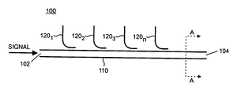
- the predetermined positions along the doped waveguide at which the coupling elements are locatedare selected so that the pump power between adjacent ones of the coupling elements decreases by at least about 3 dB.
- FIG. 5shows another embodiment of the invention that employs a pump distribution network that receives pump energy from a single pump source.
- FIG. 7shows an embodiment of the invention that employs three pump lasers and three optical coupling elements.
- the length, and hence the overall achievable gain, of a waveguide optical amplifiercan be increased by injecting pump energy at multiple points along the waveguide.
- additional pump energyis injected into the waveguide at those points along its length where the previously injected pump energy falls to an undesirably low level because of both scattering of the pump energy and the operational conditions of the amplifier.
- pump distribution network 540may be as simple as a 1 ⁇ N splitter with N waveguides for conveying the pump energy from the splitter to the coupling elements, more complex arrangements providing additional functionality are also contemplated.
- FIG. 6shows a pump distribution network 640 that receives pump energy from two or pump sources 650 1 , 650 2 , 650 3 , . . . 650 m and distributes it among pump transfer waveguides 646 1 , 646 2 , 646 3 , . . . 646 n .
- pump sources 650 1 , 650 2 , 650 3 , . . . 650 nmay be single or multimode sources.
Landscapes
- Physics & Mathematics (AREA)
- Electromagnetism (AREA)
- Engineering & Computer Science (AREA)
- Plasma & Fusion (AREA)
- Optics & Photonics (AREA)
- Lasers (AREA)
Abstract
Description
Pout=Pin−α*L1 (1)
where h is Plank's constant, ν is the pump optical frequency, A is the pump modal cross-section area (10 μm2), σais the absorption optical cross-section (10−21cm2), and τ is the excited state lifetime (10 msec). In this case the optimum value of L1is given by
Claims (50)
Priority Applications (1)
| Application Number | Priority Date | Filing Date | Title |
|---|---|---|---|
| US10/818,672US7027212B2 (en) | 2002-01-31 | 2004-04-06 | Waveguide optical amplifier |
Applications Claiming Priority (2)
| Application Number | Priority Date | Filing Date | Title |
|---|---|---|---|
| US10/066,283US20030142388A1 (en) | 2002-01-31 | 2002-01-31 | Waveguide optical amplifier |
| US10/818,672US7027212B2 (en) | 2002-01-31 | 2004-04-06 | Waveguide optical amplifier |
Related Parent Applications (1)
| Application Number | Title | Priority Date | Filing Date |
|---|---|---|---|
| US10/066,283ContinuationUS20030142388A1 (en) | 2002-01-31 | 2002-01-31 | Waveguide optical amplifier |
Publications (2)
| Publication Number | Publication Date |
|---|---|
| US20040257639A1 US20040257639A1 (en) | 2004-12-23 |
| US7027212B2true US7027212B2 (en) | 2006-04-11 |
Family
ID=27610464
Family Applications (2)
| Application Number | Title | Priority Date | Filing Date |
|---|---|---|---|
| US10/066,283AbandonedUS20030142388A1 (en) | 2002-01-31 | 2002-01-31 | Waveguide optical amplifier |
| US10/818,672Expired - LifetimeUS7027212B2 (en) | 2002-01-31 | 2004-04-06 | Waveguide optical amplifier |
Family Applications Before (1)
| Application Number | Title | Priority Date | Filing Date |
|---|---|---|---|
| US10/066,283AbandonedUS20030142388A1 (en) | 2002-01-31 | 2002-01-31 | Waveguide optical amplifier |
Country Status (1)
| Country | Link |
|---|---|
| US (2) | US20030142388A1 (en) |
Cited By (3)
| Publication number | Priority date | Publication date | Assignee | Title |
|---|---|---|---|---|
| US20050226590A1 (en)* | 2004-04-07 | 2005-10-13 | Patel Falgun D | Variable optical attenuator based on rare earth doped glass |
| US20130314770A1 (en)* | 2011-02-10 | 2013-11-28 | Soreqnuclear Research Center | High power planar lasing waveguide |
| CN105308487A (en)* | 2014-04-17 | 2016-02-03 | 华为技术有限公司 | Optical waveguide and printed circuit board |
Families Citing this family (1)
| Publication number | Priority date | Publication date | Assignee | Title |
|---|---|---|---|---|
| CN109075521A (en)* | 2016-05-13 | 2018-12-21 | 三菱电机株式会社 | Optical amplification device |
Citations (16)
| Publication number | Priority date | Publication date | Assignee | Title |
|---|---|---|---|---|
| US5253104A (en) | 1992-09-15 | 1993-10-12 | At&T Bell Laboratories | Balanced optical amplifier |
| US5430572A (en) | 1993-09-30 | 1995-07-04 | At&T Corp. | High power, high gain, low noise, two-stage optical amplifier |
| US5719976A (en) | 1995-10-24 | 1998-02-17 | Lucent Technologies, Inc. | Optimized waveguide structure |
| US5768452A (en) | 1996-04-17 | 1998-06-16 | Lucent Technologies Inc. | Radiolytic method for trimming planar waveguide couplers |
| US5887097A (en) | 1997-07-21 | 1999-03-23 | Lucent Technologies Inc. | Apparatus for pumping an optical fiber laser |
| US5930029A (en) | 1997-12-02 | 1999-07-27 | Sdl, Inc. | Optical fiber amplifier with optimized power conversion |
| US5985685A (en) | 1994-02-24 | 1999-11-16 | British Telecommunications Public Limited Company | Method for making optical device with composite passive and tapered active waveguide regions |
| US5995275A (en)* | 1996-02-26 | 1999-11-30 | Fujitsu, Ltd. | Doped fiber amplifier using bidirectional pumping with pump lights having different frequencies |
| US6043929A (en) | 1998-03-16 | 2000-03-28 | Lucent Technologies, Inc. | Adiabatic waveguide amplifier |
| US6052397A (en) | 1997-12-05 | 2000-04-18 | Sdl, Inc. | Laser diode device having a substantially circular light output beam and a method of forming a tapered section in a semiconductor device to provide for a reproducible mode profile of the output beam |
| US6157765A (en) | 1998-11-03 | 2000-12-05 | Lucent Technologies | Planar waveguide optical amplifier |
| US6293688B1 (en) | 1999-11-12 | 2001-09-25 | Sparkolor Corporation | Tapered optical waveguide coupler |
| US6493476B2 (en) | 2000-11-27 | 2002-12-10 | Teem Photonics | Apparatus and method for integrated photonic devices having gain and wavelength-selectivity |
| US6549688B2 (en) | 2001-07-06 | 2003-04-15 | Redfern Integrated Optics Pty Ltd | Monolithically-integrated optical device and method of forming same |
| WO2003076990A1 (en)* | 2002-03-04 | 2003-09-18 | Inplane Photonics, Inc. | Optical module formed on a planar lightguide circuit including a waveguide optical amplifier |
| US6721087B2 (en)* | 2001-12-13 | 2004-04-13 | Intel Corporation | Optical amplifier with distributed evanescently-coupled pump |
- 2002
- 2002-01-31USUS10/066,283patent/US20030142388A1/ennot_activeAbandoned
- 2004
- 2004-04-06USUS10/818,672patent/US7027212B2/ennot_activeExpired - Lifetime
Patent Citations (16)
| Publication number | Priority date | Publication date | Assignee | Title |
|---|---|---|---|---|
| US5253104A (en) | 1992-09-15 | 1993-10-12 | At&T Bell Laboratories | Balanced optical amplifier |
| US5430572A (en) | 1993-09-30 | 1995-07-04 | At&T Corp. | High power, high gain, low noise, two-stage optical amplifier |
| US5985685A (en) | 1994-02-24 | 1999-11-16 | British Telecommunications Public Limited Company | Method for making optical device with composite passive and tapered active waveguide regions |
| US5719976A (en) | 1995-10-24 | 1998-02-17 | Lucent Technologies, Inc. | Optimized waveguide structure |
| US5995275A (en)* | 1996-02-26 | 1999-11-30 | Fujitsu, Ltd. | Doped fiber amplifier using bidirectional pumping with pump lights having different frequencies |
| US5768452A (en) | 1996-04-17 | 1998-06-16 | Lucent Technologies Inc. | Radiolytic method for trimming planar waveguide couplers |
| US5887097A (en) | 1997-07-21 | 1999-03-23 | Lucent Technologies Inc. | Apparatus for pumping an optical fiber laser |
| US5930029A (en) | 1997-12-02 | 1999-07-27 | Sdl, Inc. | Optical fiber amplifier with optimized power conversion |
| US6052397A (en) | 1997-12-05 | 2000-04-18 | Sdl, Inc. | Laser diode device having a substantially circular light output beam and a method of forming a tapered section in a semiconductor device to provide for a reproducible mode profile of the output beam |
| US6043929A (en) | 1998-03-16 | 2000-03-28 | Lucent Technologies, Inc. | Adiabatic waveguide amplifier |
| US6157765A (en) | 1998-11-03 | 2000-12-05 | Lucent Technologies | Planar waveguide optical amplifier |
| US6293688B1 (en) | 1999-11-12 | 2001-09-25 | Sparkolor Corporation | Tapered optical waveguide coupler |
| US6493476B2 (en) | 2000-11-27 | 2002-12-10 | Teem Photonics | Apparatus and method for integrated photonic devices having gain and wavelength-selectivity |
| US6549688B2 (en) | 2001-07-06 | 2003-04-15 | Redfern Integrated Optics Pty Ltd | Monolithically-integrated optical device and method of forming same |
| US6721087B2 (en)* | 2001-12-13 | 2004-04-13 | Intel Corporation | Optical amplifier with distributed evanescently-coupled pump |
| WO2003076990A1 (en)* | 2002-03-04 | 2003-09-18 | Inplane Photonics, Inc. | Optical module formed on a planar lightguide circuit including a waveguide optical amplifier |
Cited By (5)
| Publication number | Priority date | Publication date | Assignee | Title |
|---|---|---|---|---|
| US20050226590A1 (en)* | 2004-04-07 | 2005-10-13 | Patel Falgun D | Variable optical attenuator based on rare earth doped glass |
| US20130314770A1 (en)* | 2011-02-10 | 2013-11-28 | Soreqnuclear Research Center | High power planar lasing waveguide |
| US9343864B2 (en)* | 2011-02-10 | 2016-05-17 | Soreq Nuclear Research Center | High power planar lasing waveguide |
| CN105308487A (en)* | 2014-04-17 | 2016-02-03 | 华为技术有限公司 | Optical waveguide and printed circuit board |
| CN105308487B (en)* | 2014-04-17 | 2018-09-21 | 华为技术有限公司 | A kind of optical waveguide and printed circuit board |
Also Published As
| Publication number | Publication date |
|---|---|
| US20040257639A1 (en) | 2004-12-23 |
| US20030142388A1 (en) | 2003-07-31 |
Similar Documents
| Publication | Publication Date | Title |
|---|---|---|
| US6836607B2 (en) | Cladding-pumped 3-level fiber laser/amplifier | |
| US5768012A (en) | Apparatus and method for the high-power pumping of fiber optic amplifiers | |
| US5933437A (en) | Optical fiber laser | |
| US7679818B2 (en) | Optical switch using rare earth doped glass | |
| Hübner et al. | Planar Er-and Yb-doped amplifiers and lasers | |
| US5128801A (en) | Integrated optical signal amplifier | |
| KR100634208B1 (en) | Fiber Optics and Fiber Amplifiers Using the Same | |
| US6865018B2 (en) | Multistage optical amplifier having a fiber-based amplifier stage and a planar waveguide-based amplifier stage | |
| US7027212B2 (en) | Waveguide optical amplifier | |
| EP0440049B1 (en) | Integrated optical signal amplifier | |
| US7180656B2 (en) | Compact optical amplifier | |
| US20080130100A1 (en) | High-efficiency, high-reliability fiber amplifier using engineered passband of photonic bandgap optical fiber | |
| US6888668B2 (en) | Optical amplifier with multiple wavelength pump | |
| EP1672822B1 (en) | Optical fibre for an optical amplifier with rare earth element amplification and Raman optical amplification | |
| KR20000027961A (en) | Optical element using core in which erbium ion and thorium ion are added | |
| US6661567B2 (en) | Optical amplifier, optical amplifier hybrid assembly and method of manufacture | |
| JPH11145539A5 (en) | ||
| US20050226590A1 (en) | Variable optical attenuator based on rare earth doped glass | |
| US7209283B2 (en) | Compact optical amplifier with a flattened gain profile | |
| JP3055235B2 (en) | Optical circuit manufacturing method | |
| JP2003149481A (en) | Optical amplifier-integrated waveguide | |
| JPH04271328A (en) | Production of optical waveguide for optical amplifier | |
| Kondo et al. | Broadband amplification of Er-doped bismuthate waveguide with> 10 dBm output powers from 1527 to 1573 nm | |
| JPH0537047A (en) | Optical active device | |
| CA2244160A1 (en) | High gain, high power, low noise optical waveguide amplifiers |
Legal Events
| Date | Code | Title | Description |
|---|---|---|---|
| STCF | Information on status: patent grant | Free format text:PATENTED CASE | |
| AS | Assignment | Owner name:COMERICA BANK, CALIFORNIA Free format text:SECURITY AGREEMENT;ASSIGNOR:INPLANE PHOTONICS, INC.;REEL/FRAME:020393/0753 Effective date:20080102 | |
| AS | Assignment | Owner name:INPLANE PHOTONICS INC., PENNSYLVANIA Free format text:RELEASE BY SECURED PARTY;ASSIGNOR:COMERICA BANK;REEL/FRAME:021018/0664 Effective date:20080527 | |
| AS | Assignment | Owner name:CYOPTICS, INC., PENNSYLVANIA Free format text:MERGER;ASSIGNOR:INPLANE PHOTONICS, INC.;REEL/FRAME:021205/0476 Effective date:20001128 | |
| FPAY | Fee payment | Year of fee payment:4 | |
| AS | Assignment | Owner name:SILICON VALLEY BANK, CALIFORNIA Free format text:SECURITY AGREEMENT;ASSIGNOR:CYOPTICS, INC.;REEL/FRAME:023741/0945 Effective date:20091231 | |
| FEPP | Fee payment procedure | Free format text:PAT HOLDER NO LONGER CLAIMS SMALL ENTITY STATUS, ENTITY STATUS SET TO UNDISCOUNTED (ORIGINAL EVENT CODE: STOL); ENTITY STATUS OF PATENT OWNER: LARGE ENTITY | |
| AS | Assignment | Owner name:CYOPTICS, INC., PENNSYLVANIA Free format text:RELEASE BY SECURED PARTY;ASSIGNOR:SILICON VALLEY BANK;REEL/FRAME:030707/0468 Effective date:20130628 | |
| FPAY | Fee payment | Year of fee payment:8 | |
| AS | Assignment | Owner name:AVAGO TECHNOLOGIES GENERAL IP (SINGAPORE) PTE. LTD Free format text:ASSIGNMENT OF ASSIGNORS INTEREST;ASSIGNOR:CYOPTICS, INC.;REEL/FRAME:032159/0790 Effective date:20140106 | |
| AS | Assignment | Owner name:DEUTSCHE BANK AG NEW YORK BRANCH, AS COLLATERAL AGENT, NEW YORK Free format text:PATENT SECURITY AGREEMENT;ASSIGNOR:AVAGO TECHNOLOGIES GENERAL IP (SINGAPORE) PTE. LTD.;REEL/FRAME:032851/0001 Effective date:20140506 Owner name:DEUTSCHE BANK AG NEW YORK BRANCH, AS COLLATERAL AG Free format text:PATENT SECURITY AGREEMENT;ASSIGNOR:AVAGO TECHNOLOGIES GENERAL IP (SINGAPORE) PTE. LTD.;REEL/FRAME:032851/0001 Effective date:20140506 | |
| AS | Assignment | Owner name:AVAGO TECHNOLOGIES GENERAL IP (SINGAPORE) PTE. LTD., SINGAPORE Free format text:TERMINATION AND RELEASE OF SECURITY INTEREST IN PATENT RIGHTS (RELEASES RF 032851-0001);ASSIGNOR:DEUTSCHE BANK AG NEW YORK BRANCH, AS COLLATERAL AGENT;REEL/FRAME:037689/0001 Effective date:20160201 Owner name:AVAGO TECHNOLOGIES GENERAL IP (SINGAPORE) PTE. LTD Free format text:TERMINATION AND RELEASE OF SECURITY INTEREST IN PATENT RIGHTS (RELEASES RF 032851-0001);ASSIGNOR:DEUTSCHE BANK AG NEW YORK BRANCH, AS COLLATERAL AGENT;REEL/FRAME:037689/0001 Effective date:20160201 | |
| AS | Assignment | Owner name:BANK OF AMERICA, N.A., AS COLLATERAL AGENT, NORTH CAROLINA Free format text:PATENT SECURITY AGREEMENT;ASSIGNOR:AVAGO TECHNOLOGIES GENERAL IP (SINGAPORE) PTE. LTD.;REEL/FRAME:037808/0001 Effective date:20160201 Owner name:BANK OF AMERICA, N.A., AS COLLATERAL AGENT, NORTH Free format text:PATENT SECURITY AGREEMENT;ASSIGNOR:AVAGO TECHNOLOGIES GENERAL IP (SINGAPORE) PTE. LTD.;REEL/FRAME:037808/0001 Effective date:20160201 | |
| AS | Assignment | Owner name:AVAGO TECHNOLOGIES GENERAL IP (SINGAPORE) PTE. LTD., SINGAPORE Free format text:TERMINATION AND RELEASE OF SECURITY INTEREST IN PATENTS;ASSIGNOR:BANK OF AMERICA, N.A., AS COLLATERAL AGENT;REEL/FRAME:041710/0001 Effective date:20170119 Owner name:AVAGO TECHNOLOGIES GENERAL IP (SINGAPORE) PTE. LTD Free format text:TERMINATION AND RELEASE OF SECURITY INTEREST IN PATENTS;ASSIGNOR:BANK OF AMERICA, N.A., AS COLLATERAL AGENT;REEL/FRAME:041710/0001 Effective date:20170119 | |
| MAFP | Maintenance fee payment | Free format text:PAYMENT OF MAINTENANCE FEE, 12TH YEAR, LARGE ENTITY (ORIGINAL EVENT CODE: M1553) Year of fee payment:12 | |
| AS | Assignment | Owner name:AVAGO TECHNOLOGIES INTERNATIONAL SALES PTE. LIMITE Free format text:MERGER;ASSIGNOR:AVAGO TECHNOLOGIES GENERAL IP (SINGAPORE) PTE. LTD.;REEL/FRAME:047196/0097 Effective date:20180509 | |
| AS | Assignment | Owner name:AVAGO TECHNOLOGIES INTERNATIONAL SALES PTE. LIMITE Free format text:CORRECTIVE ASSIGNMENT TO CORRECT THE EXECUTION DATE PREVIOUSLY RECORDED AT REEL: 047196 FRAME: 0097. ASSIGNOR(S) HEREBY CONFIRMS THE MERGER;ASSIGNOR:AVAGO TECHNOLOGIES GENERAL IP (SINGAPORE) PTE. LTD.;REEL/FRAME:048555/0510 Effective date:20180905 | |
| AS | Assignment | Owner name:BROADCOM INTERNATIONAL PTE. LTD., SINGAPORE Free format text:ASSIGNMENT OF ASSIGNORS INTEREST;ASSIGNOR:AVAGO TECHNOLOGIES INTERNATIONAL SALES PTE. LIMITED;REEL/FRAME:053771/0901 Effective date:20200826 |