US7027155B2 - Methods and systems for precisely relatively positioning a waist of a pulsed laser beam and method and system for controlling energy delivered to a target structure - Google Patents
Methods and systems for precisely relatively positioning a waist of a pulsed laser beam and method and system for controlling energy delivered to a target structureDownload PDFInfo
- Publication number
- US7027155B2 US7027155B2US10/107,702US10770202AUS7027155B2US 7027155 B2US7027155 B2US 7027155B2US 10770202 AUS10770202 AUS 10770202AUS 7027155 B2US7027155 B2US 7027155B2
- Authority
- US
- United States
- Prior art keywords
- laser
- pulse
- target
- target material
- substrate
- Prior art date
- Legal status (The legal status is an assumption and is not a legal conclusion. Google has not performed a legal analysis and makes no representation as to the accuracy of the status listed.)
- Expired - Fee Related, expires
Links
- 238000000034methodMethods0.000titleclaimsabstractdescription139
- 239000000758substrateSubstances0.000claimsabstractdescription90
- 238000012545processingMethods0.000claimsabstractdescription65
- 230000008569processEffects0.000claimsabstractdescription49
- 230000001678irradiating effectEffects0.000claimsabstractdescription20
- 238000005259measurementMethods0.000claimsdescription83
- 239000000463materialSubstances0.000claimsdescription55
- 230000003287optical effectEffects0.000claimsdescription52
- 230000010287polarizationEffects0.000claimsdescription41
- 230000033001locomotionEffects0.000claimsdescription30
- 239000004065semiconductorSubstances0.000claimsdescription26
- 239000013077target materialSubstances0.000claimsdescription24
- 230000015654memoryEffects0.000claimsdescription16
- XUIMIQQOPSSXEZ-UHFFFAOYSA-NSiliconChemical compound[Si]XUIMIQQOPSSXEZ-UHFFFAOYSA-N0.000claimsdescription14
- 229910052710siliconInorganic materials0.000claimsdescription14
- 239000010703siliconSubstances0.000claimsdescription14
- 230000001965increasing effectEffects0.000claimsdescription8
- 230000001939inductive effectEffects0.000claimsdescription7
- 230000003993interactionEffects0.000abstractdescription17
- 239000010410layerSubstances0.000description148
- 230000006378damageEffects0.000description29
- 239000010949copperSubstances0.000description27
- VYPSYNLAJGMNEJ-UHFFFAOYSA-NSilicium dioxideChemical compoundO=[Si]=OVYPSYNLAJGMNEJ-UHFFFAOYSA-N0.000description26
- 238000010521absorption reactionMethods0.000description25
- 229910052802copperInorganic materials0.000description25
- 238000002310reflectometryMethods0.000description25
- 230000002123temporal effectEffects0.000description24
- RYGMFSIKBFXOCR-UHFFFAOYSA-NCopperChemical compound[Cu]RYGMFSIKBFXOCR-UHFFFAOYSA-N0.000description23
- 238000004140cleaningMethods0.000description22
- HQVNEWCFYHHQES-UHFFFAOYSA-Nsilicon nitrideChemical compoundN12[Si]34N5[Si]62N3[Si]51N64HQVNEWCFYHHQES-UHFFFAOYSA-N0.000description18
- 235000012431wafersNutrition0.000description17
- 230000005540biological transmissionEffects0.000description15
- 230000000694effectsEffects0.000description13
- 229910052751metalInorganic materials0.000description13
- 239000002184metalSubstances0.000description13
- 230000003111delayed effectEffects0.000description10
- 238000013461designMethods0.000description10
- 230000002829reductive effectEffects0.000description10
- 230000008901benefitEffects0.000description9
- 239000004020conductorSubstances0.000description9
- 238000010586diagramMethods0.000description8
- 239000000835fiberSubstances0.000description8
- 230000001976improved effectEffects0.000description8
- 238000007493shaping processMethods0.000description8
- 239000000377silicon dioxideSubstances0.000description8
- 235000012239silicon dioxideNutrition0.000description8
- 229910052581Si3N4Inorganic materials0.000description7
- 230000008878couplingEffects0.000description7
- 238000010168coupling processMethods0.000description7
- 238000005859coupling reactionMethods0.000description7
- 230000003247decreasing effectEffects0.000description7
- 238000005516engineering processMethods0.000description7
- 230000008439repair processEffects0.000description7
- 238000004422calculation algorithmMethods0.000description6
- 238000005336crackingMethods0.000description6
- 239000003989dielectric materialSubstances0.000description6
- 238000004519manufacturing processMethods0.000description6
- 230000005855radiationEffects0.000description6
- 230000000630rising effectEffects0.000description6
- 238000001069Raman spectroscopyMethods0.000description5
- 229910052782aluminiumInorganic materials0.000description5
- 238000013459approachMethods0.000description5
- 230000008859changeEffects0.000description5
- 238000001514detection methodMethods0.000description5
- XAGFODPZIPBFFR-UHFFFAOYSA-NaluminiumChemical compound[Al]XAGFODPZIPBFFR-UHFFFAOYSA-N0.000description4
- 230000003321amplificationEffects0.000description4
- 238000007664blowingMethods0.000description4
- 238000009826distributionMethods0.000description4
- 238000012544monitoring processMethods0.000description4
- 238000003199nucleic acid amplification methodMethods0.000description4
- BASFCYQUMIYNBI-UHFFFAOYSA-NplatinumChemical compound[Pt]BASFCYQUMIYNBI-UHFFFAOYSA-N0.000description4
- 238000004088simulationMethods0.000description4
- 239000002356single layerSubstances0.000description4
- 230000003595spectral effectEffects0.000description4
- 239000011248coating agentSubstances0.000description3
- 238000000576coating methodMethods0.000description3
- 230000001934delayEffects0.000description3
- 238000009792diffusion processMethods0.000description3
- 238000002474experimental methodMethods0.000description3
- 238000004880explosionMethods0.000description3
- 239000010408filmSubstances0.000description3
- 230000006870functionEffects0.000description3
- PCHJSUWPFVWCPO-UHFFFAOYSA-NgoldChemical compound[Au]PCHJSUWPFVWCPO-UHFFFAOYSA-N0.000description3
- 239000010931goldSubstances0.000description3
- 229910052737goldInorganic materials0.000description3
- 230000006872improvementEffects0.000description3
- 230000000670limiting effectEffects0.000description3
- 229910000679solderInorganic materials0.000description3
- 239000007787solidSubstances0.000description3
- 230000035882stressEffects0.000description3
- 101100456571Mus musculus Med12 geneProteins0.000description2
- 230000002238attenuated effectEffects0.000description2
- 230000009286beneficial effectEffects0.000description2
- 238000004364calculation methodMethods0.000description2
- 230000007423decreaseEffects0.000description2
- 230000001419dependent effectEffects0.000description2
- 230000001627detrimental effectEffects0.000description2
- 238000000572ellipsometryMethods0.000description2
- 238000010438heat treatmentMethods0.000description2
- 238000002329infrared spectrumMethods0.000description2
- 238000000691measurement methodMethods0.000description2
- 230000007246mechanismEffects0.000description2
- 238000005459micromachiningMethods0.000description2
- 229910052697platinumInorganic materials0.000description2
- 238000003672processing methodMethods0.000description2
- 239000000047productSubstances0.000description2
- 230000009467reductionEffects0.000description2
- 230000004044responseEffects0.000description2
- 238000001228spectrumMethods0.000description2
- 230000001360synchronised effectEffects0.000description2
- 230000001960triggered effectEffects0.000description2
- RTAQQCXQSZGOHL-UHFFFAOYSA-NTitaniumChemical compound[Ti]RTAQQCXQSZGOHL-UHFFFAOYSA-N0.000description1
- 230000003044adaptive effectEffects0.000description1
- 238000004458analytical methodMethods0.000description1
- 230000002547anomalous effectEffects0.000description1
- 230000008033biological extinctionEffects0.000description1
- 238000005253claddingMethods0.000description1
- 239000002131composite materialSubstances0.000description1
- 238000005094computer simulationMethods0.000description1
- 239000000356contaminantSubstances0.000description1
- 238000012937correctionMethods0.000description1
- 238000012864cross contaminationMethods0.000description1
- 238000006880cross-coupling reactionMethods0.000description1
- 239000013078crystalSubstances0.000description1
- 238000005520cutting processMethods0.000description1
- 238000011161developmentMethods0.000description1
- 230000018109developmental processEffects0.000description1
- ALKZAGKDWUSJED-UHFFFAOYSA-Ndinuclear copper ionChemical compound[Cu].[Cu]ALKZAGKDWUSJED-UHFFFAOYSA-N0.000description1
- 238000005553drillingMethods0.000description1
- 230000001747exhibiting effectEffects0.000description1
- 230000004907fluxEffects0.000description1
- 238000005286illuminationMethods0.000description1
- 238000003384imaging methodMethods0.000description1
- 238000011065in-situ storageMethods0.000description1
- 239000011810insulating materialSubstances0.000description1
- 239000012212insulatorSubstances0.000description1
- 230000010354integrationEffects0.000description1
- 239000004973liquid crystal related substanceSubstances0.000description1
- 238000001465metallisationMethods0.000description1
- 150000002739metalsChemical class0.000description1
- 238000000386microscopyMethods0.000description1
- 238000001208nuclear magnetic resonance pulse sequenceMethods0.000description1
- 238000005457optimizationMethods0.000description1
- 238000002161passivationMethods0.000description1
- 230000000704physical effectEffects0.000description1
- 238000005498polishingMethods0.000description1
- 229910021420polycrystalline siliconInorganic materials0.000description1
- 229920005591polysiliconPolymers0.000description1
- 238000011112process operationMethods0.000description1
- 230000000135prohibitive effectEffects0.000description1
- 230000001902propagating effectEffects0.000description1
- 239000011241protective layerSubstances0.000description1
- 230000000191radiation effectEffects0.000description1
- 238000011084recoveryMethods0.000description1
- 230000035945sensitivityEffects0.000description1
- 238000000926separation methodMethods0.000description1
- 230000009528severe injuryEffects0.000description1
- 230000035939shockEffects0.000description1
- 239000002210silicon-based materialSubstances0.000description1
- 239000002893slagSubstances0.000description1
- 125000006850spacer groupChemical group0.000description1
- 238000004611spectroscopical analysisMethods0.000description1
- 238000010183spectrum analysisMethods0.000description1
- 239000013589supplementSubstances0.000description1
- 230000003685thermal hair damageEffects0.000description1
- 230000008646thermal stressEffects0.000description1
- 239000010409thin filmSubstances0.000description1
- 229910052719titaniumInorganic materials0.000description1
- 239000010936titaniumSubstances0.000description1
- 230000007704transitionEffects0.000description1
- 238000013519translationMethods0.000description1
- 238000009966trimmingMethods0.000description1
- 238000009827uniform distributionMethods0.000description1
- 230000008016vaporizationEffects0.000description1
- 238000001429visible spectrumMethods0.000description1
- 239000003643water by typeSubstances0.000description1
- 229910052724xenonInorganic materials0.000description1
- FHNFHKCVQCLJFQ-UHFFFAOYSA-Nxenon atomChemical compound[Xe]FHNFHKCVQCLJFQ-UHFFFAOYSA-N0.000description1
- 229910052727yttriumInorganic materials0.000description1
Images


Classifications
- H—ELECTRICITY
- H10—SEMICONDUCTOR DEVICES; ELECTRIC SOLID-STATE DEVICES NOT OTHERWISE PROVIDED FOR
- H10D—INORGANIC ELECTRIC SEMICONDUCTOR DEVICES
- H10D84/00—Integrated devices formed in or on semiconductor substrates that comprise only semiconducting layers, e.g. on Si wafers or on GaAs-on-Si wafers
- H10D84/01—Manufacture or treatment
- B—PERFORMING OPERATIONS; TRANSPORTING
- B23—MACHINE TOOLS; METAL-WORKING NOT OTHERWISE PROVIDED FOR
- B23K—SOLDERING OR UNSOLDERING; WELDING; CLADDING OR PLATING BY SOLDERING OR WELDING; CUTTING BY APPLYING HEAT LOCALLY, e.g. FLAME CUTTING; WORKING BY LASER BEAM
- B23K26/00—Working by laser beam, e.g. welding, cutting or boring
- B23K26/02—Positioning or observing the workpiece, e.g. with respect to the point of impact; Aligning, aiming or focusing the laser beam
- B23K26/06—Shaping the laser beam, e.g. by masks or multi-focusing
- B23K26/073—Shaping the laser spot
- B23K26/0736—Shaping the laser spot into an oval shape, e.g. elliptic shape
- B—PERFORMING OPERATIONS; TRANSPORTING
- B23—MACHINE TOOLS; METAL-WORKING NOT OTHERWISE PROVIDED FOR
- B23K—SOLDERING OR UNSOLDERING; WELDING; CLADDING OR PLATING BY SOLDERING OR WELDING; CUTTING BY APPLYING HEAT LOCALLY, e.g. FLAME CUTTING; WORKING BY LASER BEAM
- B23K26/00—Working by laser beam, e.g. welding, cutting or boring
- B23K26/02—Positioning or observing the workpiece, e.g. with respect to the point of impact; Aligning, aiming or focusing the laser beam
- B23K26/03—Observing, e.g. monitoring, the workpiece
- B23K26/032—Observing, e.g. monitoring, the workpiece using optical means
- B—PERFORMING OPERATIONS; TRANSPORTING
- B23—MACHINE TOOLS; METAL-WORKING NOT OTHERWISE PROVIDED FOR
- B23K—SOLDERING OR UNSOLDERING; WELDING; CLADDING OR PLATING BY SOLDERING OR WELDING; CUTTING BY APPLYING HEAT LOCALLY, e.g. FLAME CUTTING; WORKING BY LASER BEAM
- B23K26/00—Working by laser beam, e.g. welding, cutting or boring
- B23K26/02—Positioning or observing the workpiece, e.g. with respect to the point of impact; Aligning, aiming or focusing the laser beam
- B23K26/04—Automatically aligning, aiming or focusing the laser beam, e.g. using the back-scattered light
- B23K26/042—Automatically aligning the laser beam
- B23K26/043—Automatically aligning the laser beam along the beam path, i.e. alignment of laser beam axis relative to laser beam apparatus
- B—PERFORMING OPERATIONS; TRANSPORTING
- B23—MACHINE TOOLS; METAL-WORKING NOT OTHERWISE PROVIDED FOR
- B23K—SOLDERING OR UNSOLDERING; WELDING; CLADDING OR PLATING BY SOLDERING OR WELDING; CUTTING BY APPLYING HEAT LOCALLY, e.g. FLAME CUTTING; WORKING BY LASER BEAM
- B23K26/00—Working by laser beam, e.g. welding, cutting or boring
- B23K26/02—Positioning or observing the workpiece, e.g. with respect to the point of impact; Aligning, aiming or focusing the laser beam
- B23K26/06—Shaping the laser beam, e.g. by masks or multi-focusing
- B23K26/0604—Shaping the laser beam, e.g. by masks or multi-focusing by a combination of beams
- B23K26/0613—Shaping the laser beam, e.g. by masks or multi-focusing by a combination of beams having a common axis
- B—PERFORMING OPERATIONS; TRANSPORTING
- B23—MACHINE TOOLS; METAL-WORKING NOT OTHERWISE PROVIDED FOR
- B23K—SOLDERING OR UNSOLDERING; WELDING; CLADDING OR PLATING BY SOLDERING OR WELDING; CUTTING BY APPLYING HEAT LOCALLY, e.g. FLAME CUTTING; WORKING BY LASER BEAM
- B23K26/00—Working by laser beam, e.g. welding, cutting or boring
- B23K26/02—Positioning or observing the workpiece, e.g. with respect to the point of impact; Aligning, aiming or focusing the laser beam
- B23K26/06—Shaping the laser beam, e.g. by masks or multi-focusing
- B23K26/062—Shaping the laser beam, e.g. by masks or multi-focusing by direct control of the laser beam
- B23K26/0622—Shaping the laser beam, e.g. by masks or multi-focusing by direct control of the laser beam by shaping pulses
- B23K26/0624—Shaping the laser beam, e.g. by masks or multi-focusing by direct control of the laser beam by shaping pulses using ultrashort pulses, i.e. pulses of 1ns or less
- B—PERFORMING OPERATIONS; TRANSPORTING
- B23—MACHINE TOOLS; METAL-WORKING NOT OTHERWISE PROVIDED FOR
- B23K—SOLDERING OR UNSOLDERING; WELDING; CLADDING OR PLATING BY SOLDERING OR WELDING; CUTTING BY APPLYING HEAT LOCALLY, e.g. FLAME CUTTING; WORKING BY LASER BEAM
- B23K26/00—Working by laser beam, e.g. welding, cutting or boring
- B23K26/02—Positioning or observing the workpiece, e.g. with respect to the point of impact; Aligning, aiming or focusing the laser beam
- B23K26/06—Shaping the laser beam, e.g. by masks or multi-focusing
- B23K26/064—Shaping the laser beam, e.g. by masks or multi-focusing by means of optical elements, e.g. lenses, mirrors or prisms
- B23K26/0643—Shaping the laser beam, e.g. by masks or multi-focusing by means of optical elements, e.g. lenses, mirrors or prisms comprising mirrors
- B—PERFORMING OPERATIONS; TRANSPORTING
- B23—MACHINE TOOLS; METAL-WORKING NOT OTHERWISE PROVIDED FOR
- B23K—SOLDERING OR UNSOLDERING; WELDING; CLADDING OR PLATING BY SOLDERING OR WELDING; CUTTING BY APPLYING HEAT LOCALLY, e.g. FLAME CUTTING; WORKING BY LASER BEAM
- B23K26/00—Working by laser beam, e.g. welding, cutting or boring
- B23K26/02—Positioning or observing the workpiece, e.g. with respect to the point of impact; Aligning, aiming or focusing the laser beam
- B23K26/06—Shaping the laser beam, e.g. by masks or multi-focusing
- B23K26/064—Shaping the laser beam, e.g. by masks or multi-focusing by means of optical elements, e.g. lenses, mirrors or prisms
- B23K26/0648—Shaping the laser beam, e.g. by masks or multi-focusing by means of optical elements, e.g. lenses, mirrors or prisms comprising lenses
- B—PERFORMING OPERATIONS; TRANSPORTING
- B23—MACHINE TOOLS; METAL-WORKING NOT OTHERWISE PROVIDED FOR
- B23K—SOLDERING OR UNSOLDERING; WELDING; CLADDING OR PLATING BY SOLDERING OR WELDING; CUTTING BY APPLYING HEAT LOCALLY, e.g. FLAME CUTTING; WORKING BY LASER BEAM
- B23K26/00—Working by laser beam, e.g. welding, cutting or boring
- B23K26/02—Positioning or observing the workpiece, e.g. with respect to the point of impact; Aligning, aiming or focusing the laser beam
- B23K26/06—Shaping the laser beam, e.g. by masks or multi-focusing
- B23K26/064—Shaping the laser beam, e.g. by masks or multi-focusing by means of optical elements, e.g. lenses, mirrors or prisms
- B23K26/0652—Shaping the laser beam, e.g. by masks or multi-focusing by means of optical elements, e.g. lenses, mirrors or prisms comprising prisms
- B—PERFORMING OPERATIONS; TRANSPORTING
- B23—MACHINE TOOLS; METAL-WORKING NOT OTHERWISE PROVIDED FOR
- B23K—SOLDERING OR UNSOLDERING; WELDING; CLADDING OR PLATING BY SOLDERING OR WELDING; CUTTING BY APPLYING HEAT LOCALLY, e.g. FLAME CUTTING; WORKING BY LASER BEAM
- B23K26/00—Working by laser beam, e.g. welding, cutting or boring
- B23K26/02—Positioning or observing the workpiece, e.g. with respect to the point of impact; Aligning, aiming or focusing the laser beam
- B23K26/06—Shaping the laser beam, e.g. by masks or multi-focusing
- B23K26/0665—Shaping the laser beam, e.g. by masks or multi-focusing by beam condensation on the workpiece, e.g. for focusing
- B—PERFORMING OPERATIONS; TRANSPORTING
- B23—MACHINE TOOLS; METAL-WORKING NOT OTHERWISE PROVIDED FOR
- B23K—SOLDERING OR UNSOLDERING; WELDING; CLADDING OR PLATING BY SOLDERING OR WELDING; CUTTING BY APPLYING HEAT LOCALLY, e.g. FLAME CUTTING; WORKING BY LASER BEAM
- B23K26/00—Working by laser beam, e.g. welding, cutting or boring
- B23K26/02—Positioning or observing the workpiece, e.g. with respect to the point of impact; Aligning, aiming or focusing the laser beam
- B23K26/06—Shaping the laser beam, e.g. by masks or multi-focusing
- B23K26/067—Dividing the beam into multiple beams, e.g. multifocusing
- B—PERFORMING OPERATIONS; TRANSPORTING
- B23—MACHINE TOOLS; METAL-WORKING NOT OTHERWISE PROVIDED FOR
- B23K—SOLDERING OR UNSOLDERING; WELDING; CLADDING OR PLATING BY SOLDERING OR WELDING; CUTTING BY APPLYING HEAT LOCALLY, e.g. FLAME CUTTING; WORKING BY LASER BEAM
- B23K26/00—Working by laser beam, e.g. welding, cutting or boring
- B23K26/08—Devices involving relative movement between laser beam and workpiece
- B23K26/082—Scanning systems, i.e. devices involving movement of the laser beam relative to the laser head
- B—PERFORMING OPERATIONS; TRANSPORTING
- B23—MACHINE TOOLS; METAL-WORKING NOT OTHERWISE PROVIDED FOR
- B23K—SOLDERING OR UNSOLDERING; WELDING; CLADDING OR PLATING BY SOLDERING OR WELDING; CUTTING BY APPLYING HEAT LOCALLY, e.g. FLAME CUTTING; WORKING BY LASER BEAM
- B23K26/00—Working by laser beam, e.g. welding, cutting or boring
- B23K26/08—Devices involving relative movement between laser beam and workpiece
- B23K26/10—Devices involving relative movement between laser beam and workpiece using a fixed support, i.e. involving moving the laser beam
- B—PERFORMING OPERATIONS; TRANSPORTING
- B23—MACHINE TOOLS; METAL-WORKING NOT OTHERWISE PROVIDED FOR
- B23K—SOLDERING OR UNSOLDERING; WELDING; CLADDING OR PLATING BY SOLDERING OR WELDING; CUTTING BY APPLYING HEAT LOCALLY, e.g. FLAME CUTTING; WORKING BY LASER BEAM
- B23K26/00—Working by laser beam, e.g. welding, cutting or boring
- B23K26/16—Removal of by-products, e.g. particles or vapours produced during treatment of a workpiece
- B—PERFORMING OPERATIONS; TRANSPORTING
- B23—MACHINE TOOLS; METAL-WORKING NOT OTHERWISE PROVIDED FOR
- B23K—SOLDERING OR UNSOLDERING; WELDING; CLADDING OR PLATING BY SOLDERING OR WELDING; CUTTING BY APPLYING HEAT LOCALLY, e.g. FLAME CUTTING; WORKING BY LASER BEAM
- B23K26/00—Working by laser beam, e.g. welding, cutting or boring
- B23K26/36—Removing material
- B23K26/361—Removing material for deburring or mechanical trimming
- B—PERFORMING OPERATIONS; TRANSPORTING
- B23—MACHINE TOOLS; METAL-WORKING NOT OTHERWISE PROVIDED FOR
- B23K—SOLDERING OR UNSOLDERING; WELDING; CLADDING OR PLATING BY SOLDERING OR WELDING; CUTTING BY APPLYING HEAT LOCALLY, e.g. FLAME CUTTING; WORKING BY LASER BEAM
- B23K26/00—Working by laser beam, e.g. welding, cutting or boring
- B23K26/36—Removing material
- B23K26/38—Removing material by boring or cutting
- B23K26/382—Removing material by boring or cutting by boring
- B23K26/389—Removing material by boring or cutting by boring of fluid openings, e.g. nozzles, jets
- B—PERFORMING OPERATIONS; TRANSPORTING
- B23—MACHINE TOOLS; METAL-WORKING NOT OTHERWISE PROVIDED FOR
- B23K—SOLDERING OR UNSOLDERING; WELDING; CLADDING OR PLATING BY SOLDERING OR WELDING; CUTTING BY APPLYING HEAT LOCALLY, e.g. FLAME CUTTING; WORKING BY LASER BEAM
- B23K26/00—Working by laser beam, e.g. welding, cutting or boring
- B23K26/36—Removing material
- B23K26/40—Removing material taking account of the properties of the material involved
- H—ELECTRICITY
- H01—ELECTRIC ELEMENTS
- H01L—SEMICONDUCTOR DEVICES NOT COVERED BY CLASS H10
- H01L21/00—Processes or apparatus adapted for the manufacture or treatment of semiconductor or solid state devices or of parts thereof
- H01L21/02—Manufacture or treatment of semiconductor devices or of parts thereof
- H01L21/04—Manufacture or treatment of semiconductor devices or of parts thereof the devices having potential barriers, e.g. a PN junction, depletion layer or carrier concentration layer
- H01L21/48—Manufacture or treatment of parts, e.g. containers, prior to assembly of the devices, using processes not provided for in a single one of the groups H01L21/18 - H01L21/326 or H10D48/04 - H10D48/07
- H01L21/4814—Conductive parts
- H01L21/4846—Leads on or in insulating or insulated substrates, e.g. metallisation
- H01L21/485—Adaptation of interconnections, e.g. engineering charges, repair techniques
- H—ELECTRICITY
- H01—ELECTRIC ELEMENTS
- H01L—SEMICONDUCTOR DEVICES NOT COVERED BY CLASS H10
- H01L21/00—Processes or apparatus adapted for the manufacture or treatment of semiconductor or solid state devices or of parts thereof
- H01L21/70—Manufacture or treatment of devices consisting of a plurality of solid state components formed in or on a common substrate or of parts thereof; Manufacture of integrated circuit devices or of parts thereof
- H01L21/71—Manufacture of specific parts of devices defined in group H01L21/70
- H01L21/768—Applying interconnections to be used for carrying current between separate components within a device comprising conductors and dielectrics
- H01L21/76838—Applying interconnections to be used for carrying current between separate components within a device comprising conductors and dielectrics characterised by the formation and the after-treatment of the conductors
- H01L21/76886—Modifying permanently or temporarily the pattern or the conductivity of conductive members, e.g. formation of alloys, reduction of contact resistances
- H01L21/76888—By rendering at least a portion of the conductor non conductive, e.g. oxidation
- H—ELECTRICITY
- H01—ELECTRIC ELEMENTS
- H01L—SEMICONDUCTOR DEVICES NOT COVERED BY CLASS H10
- H01L21/00—Processes or apparatus adapted for the manufacture or treatment of semiconductor or solid state devices or of parts thereof
- H01L21/70—Manufacture or treatment of devices consisting of a plurality of solid state components formed in or on a common substrate or of parts thereof; Manufacture of integrated circuit devices or of parts thereof
- H01L21/71—Manufacture of specific parts of devices defined in group H01L21/70
- H01L21/768—Applying interconnections to be used for carrying current between separate components within a device comprising conductors and dielectrics
- H01L21/76838—Applying interconnections to be used for carrying current between separate components within a device comprising conductors and dielectrics characterised by the formation and the after-treatment of the conductors
- H01L21/76886—Modifying permanently or temporarily the pattern or the conductivity of conductive members, e.g. formation of alloys, reduction of contact resistances
- H01L21/76892—Modifying permanently or temporarily the pattern or the conductivity of conductive members, e.g. formation of alloys, reduction of contact resistances modifying the pattern
- H01L21/76894—Modifying permanently or temporarily the pattern or the conductivity of conductive members, e.g. formation of alloys, reduction of contact resistances modifying the pattern using a laser, e.g. laser cutting, laser direct writing, laser repair
- H—ELECTRICITY
- H01—ELECTRIC ELEMENTS
- H01L—SEMICONDUCTOR DEVICES NOT COVERED BY CLASS H10
- H01L23/00—Details of semiconductor or other solid state devices
- H01L23/52—Arrangements for conducting electric current within the device in operation from one component to another, i.e. interconnections, e.g. wires, lead frames
- H01L23/522—Arrangements for conducting electric current within the device in operation from one component to another, i.e. interconnections, e.g. wires, lead frames including external interconnections consisting of a multilayer structure of conductive and insulating layers inseparably formed on the semiconductor body
- H01L23/525—Arrangements for conducting electric current within the device in operation from one component to another, i.e. interconnections, e.g. wires, lead frames including external interconnections consisting of a multilayer structure of conductive and insulating layers inseparably formed on the semiconductor body with adaptable interconnections
- H01L23/5256—Arrangements for conducting electric current within the device in operation from one component to another, i.e. interconnections, e.g. wires, lead frames including external interconnections consisting of a multilayer structure of conductive and insulating layers inseparably formed on the semiconductor body with adaptable interconnections comprising fuses, i.e. connections having their state changed from conductive to non-conductive
- H01L23/5258—Arrangements for conducting electric current within the device in operation from one component to another, i.e. interconnections, e.g. wires, lead frames including external interconnections consisting of a multilayer structure of conductive and insulating layers inseparably formed on the semiconductor body with adaptable interconnections comprising fuses, i.e. connections having their state changed from conductive to non-conductive the change of state resulting from the use of an external beam, e.g. laser beam or ion beam
- B—PERFORMING OPERATIONS; TRANSPORTING
- B23—MACHINE TOOLS; METAL-WORKING NOT OTHERWISE PROVIDED FOR
- B23K—SOLDERING OR UNSOLDERING; WELDING; CLADDING OR PLATING BY SOLDERING OR WELDING; CUTTING BY APPLYING HEAT LOCALLY, e.g. FLAME CUTTING; WORKING BY LASER BEAM
- B23K2101/00—Articles made by soldering, welding or cutting
- B23K2101/36—Electric or electronic devices
- B23K2101/38—Conductors
- B—PERFORMING OPERATIONS; TRANSPORTING
- B23—MACHINE TOOLS; METAL-WORKING NOT OTHERWISE PROVIDED FOR
- B23K—SOLDERING OR UNSOLDERING; WELDING; CLADDING OR PLATING BY SOLDERING OR WELDING; CUTTING BY APPLYING HEAT LOCALLY, e.g. FLAME CUTTING; WORKING BY LASER BEAM
- B23K2101/00—Articles made by soldering, welding or cutting
- B23K2101/36—Electric or electronic devices
- B23K2101/40—Semiconductor devices
- B—PERFORMING OPERATIONS; TRANSPORTING
- B23—MACHINE TOOLS; METAL-WORKING NOT OTHERWISE PROVIDED FOR
- B23K—SOLDERING OR UNSOLDERING; WELDING; CLADDING OR PLATING BY SOLDERING OR WELDING; CUTTING BY APPLYING HEAT LOCALLY, e.g. FLAME CUTTING; WORKING BY LASER BEAM
- B23K2103/00—Materials to be soldered, welded or cut
- B23K2103/08—Non-ferrous metals or alloys
- B23K2103/10—Aluminium or alloys thereof
- B—PERFORMING OPERATIONS; TRANSPORTING
- B23—MACHINE TOOLS; METAL-WORKING NOT OTHERWISE PROVIDED FOR
- B23K—SOLDERING OR UNSOLDERING; WELDING; CLADDING OR PLATING BY SOLDERING OR WELDING; CUTTING BY APPLYING HEAT LOCALLY, e.g. FLAME CUTTING; WORKING BY LASER BEAM
- B23K2103/00—Materials to be soldered, welded or cut
- B23K2103/08—Non-ferrous metals or alloys
- B23K2103/12—Copper or alloys thereof
- B—PERFORMING OPERATIONS; TRANSPORTING
- B23—MACHINE TOOLS; METAL-WORKING NOT OTHERWISE PROVIDED FOR
- B23K—SOLDERING OR UNSOLDERING; WELDING; CLADDING OR PLATING BY SOLDERING OR WELDING; CUTTING BY APPLYING HEAT LOCALLY, e.g. FLAME CUTTING; WORKING BY LASER BEAM
- B23K2103/00—Materials to be soldered, welded or cut
- B23K2103/16—Composite materials, e.g. fibre reinforced
- B23K2103/166—Multilayered materials
- B23K2103/172—Multilayered materials wherein at least one of the layers is non-metallic
- B—PERFORMING OPERATIONS; TRANSPORTING
- B23—MACHINE TOOLS; METAL-WORKING NOT OTHERWISE PROVIDED FOR
- B23K—SOLDERING OR UNSOLDERING; WELDING; CLADDING OR PLATING BY SOLDERING OR WELDING; CUTTING BY APPLYING HEAT LOCALLY, e.g. FLAME CUTTING; WORKING BY LASER BEAM
- B23K2103/00—Materials to be soldered, welded or cut
- B23K2103/50—Inorganic material, e.g. metals, not provided for in B23K2103/02 – B23K2103/26
- H—ELECTRICITY
- H01—ELECTRIC ELEMENTS
- H01L—SEMICONDUCTOR DEVICES NOT COVERED BY CLASS H10
- H01L22/00—Testing or measuring during manufacture or treatment; Reliability measurements, i.e. testing of parts without further processing to modify the parts as such; Structural arrangements therefor
- H01L22/10—Measuring as part of the manufacturing process
- H01L22/12—Measuring as part of the manufacturing process for structural parameters, e.g. thickness, line width, refractive index, temperature, warp, bond strength, defects, optical inspection, electrical measurement of structural dimensions, metallurgic measurement of diffusions
- H—ELECTRICITY
- H01—ELECTRIC ELEMENTS
- H01L—SEMICONDUCTOR DEVICES NOT COVERED BY CLASS H10
- H01L2924/00—Indexing scheme for arrangements or methods for connecting or disconnecting semiconductor or solid-state bodies as covered by H01L24/00
- H01L2924/0001—Technical content checked by a classifier
- H01L2924/0002—Not covered by any one of groups H01L24/00, H01L24/00 and H01L2224/00
- H—ELECTRICITY
- H05—ELECTRIC TECHNIQUES NOT OTHERWISE PROVIDED FOR
- H05K—PRINTED CIRCUITS; CASINGS OR CONSTRUCTIONAL DETAILS OF ELECTRIC APPARATUS; MANUFACTURE OF ASSEMBLAGES OF ELECTRICAL COMPONENTS
- H05K3/00—Apparatus or processes for manufacturing printed circuits
- H05K3/0011—Working of insulating substrates or insulating layers
- H05K3/0017—Etching of the substrate by chemical or physical means
- H05K3/0026—Etching of the substrate by chemical or physical means by laser ablation
Definitions
- the present inventionrelates to the field of laser processing methods and systems, and specifically, to laser processing methods and systems for processing microstructures formed on substrates. This invention is particularly applicable, but not limited to, laser repair of redundant semiconductor memory devices.
- new materialssuch as aluminum, gold, and copper, coupled with the small geometry of these devices, make the problem of link removal difficult.
- the new materialsare typically metals or highly conductive composites having reflectivity that is well over 90% in the visible and near infrared wavelength regions.
- Aluminumfor example, reflects greater than 90% of the laser energy over the range from the UV through to the near infrared.
- Gold and copperreflects even more strongly in the near infrared, the wavelengths of choice used by most of the lasers repairing memories in production.
- Thermal laser processing of linksrelies on the differential thermal expansion between the oxide above the link and the link itself. This differential expansion results in a high pressure build-up of the molten link contained by the oxide. The oxide over the link is necessary to contain the link in a molten state long enough to build-up sufficient pressure to crack the oxide and explosively expel the link material. If the pressure is too low, the link will not be removed cleanly.
- Alternative laser wavelengths and laser controlstrive to increase the laser “energy window” without damaging the substrate and material contiguous to the link.
- FIGS. 2 a and 2 billustrate prior art laser processing of multi-layer structure wherein a target structure is located in proximity to a substrate, with a q-switched pulse 20 from a conventional solid state laser 21 irradiating and overfilling a target structure 23 .
- a laser spot sizeis typically significantly larger than the (target) link size which relaxes precision positioning requirements.
- a laser wavelengthis typically selected based on substrate 27 (commonly Silicon) transmission so as to allow for higher peak laser power or other system and process variations.
- a layer 28 , 25 absorption coefficientis controlled (e.g., as a transition or protective layer) and/or a wavelength selected wherein substrate damage is avoided.
- An object of the present inventionis to provide improved methods and systems for precisely relatively positioning a waist of a pulsed laser beam and method and system for controlling energy delivered to a target structure
- a method for precisely relatively positioning a waist of a pulsed laser beam to compensate for microscopic positional variations of a predetermined target having a first material to be laser processedincludes measuring position of at least one alignment target formed at a predetermined measurement location to obtain a measurement.
- the at least one alignment targetis covered by at least one layer of a second material.
- the step of measuringincludes selectively irradiating a portion of a region to be measured with a radiation cleaning beam to remove debris from the region to compensate for reflectivity variations and reduce multiplicative noise and associated signal variations at a detector.
- the methodalso includes predicting relative location of the predetermined target and a waist of the laser beam based on the measurement to obtain a predicted relative location.
- the methodfurther includes inducing relative motion between the predetermined target and the beam waist based on the predicted relative location.
- the methodfurther includes generating the laser beam including at least one pulse, and irradiating the at least one pulse into a spot on the predetermined target wherein the at least one pulse is sufficient to process the predetermined target.
- the step of measuringmay be performed in a polarization insensitive fashion.
- the methodmay further include estimating locations utilizing a multi-parameter least squares fit algorithm to obtain residuals, and the step of predicting includes evaluating the residuals.
- the first materialmay comprise metal, and the predetermined target may be part of a multi-material device having at least one outer layer of dielectric material.
- the methodmay further include the steps of measuring layer thickness or reflectivity at at least one location to obtain a layer measurement and utilizing the layer measurement to control a characteristic of the at least one pulse.
- the methodmay further include measuring a layer thickness to obtain a thickness measurement and using at least the thickness measurement for predicting the relative location.
- the characteristicmay be pulse energy or pulsewidth.
- the methodmay further include the steps of measuring layer thickness or reflectivity at at least one location to obtain a layer measurement, and utilizing the layer measurement to controllably shift a wavelength of the laser beam.
- the methodmay further include: (a) obtaining information identifying microstructures designated for removal, (b) measuring a first set of reference locations to obtain three-dimensional reference data, (c) generating a trajectory based on at least the three-dimensional reference data to obtain a prediction of beam waist and microstructure surface locations, and (d) updating the predicted relative location during relative motion based on updated position information, the updated position information being obtained during the relative motion.
- the updated position information obtained during the step of relatively positioningmay include data from a position encoder or may include data from an optical sensor.
- the step of selectively irradiatingmay occur within orthogonal linear scans in the region to be measured.
- the at least one alignment targetmay be part of a multi-material semiconductor memory including a substrate and at least one dielectric layer disposed between the substrate and the predetermined target, and power of the radiation cleaning beam may be substantially below power required to cause an undesirable change to the predetermined target, the substrate, or the at least one dielectric layer.
- Energy of the cleaning beammay be in the range 0.005 to 0.05 ⁇ joules.
- a system for precisely relatively positioning a waist of a pulsed laser beam to compensate for microscopic positional variations of a predetermined target having a first material to be laser processedincludes means for measuring position of at least one alignment target formed at a predetermined measurement location to obtain a measurement.
- the at least one alignment targetis covered by at least one layer of a second material.
- the means for measuringincludes means for selectively irradiating a portion of a region to be measured with a radiation cleaning beam to remove debris from the region to compensate for reflectivity variations and reduce multiplicative noise and associated signal variations at a detector.
- the systemalso includes means for predicting relative location of the predetermined target and a waist of the laser beam based on the measurement to obtain a predicted relative location.
- the systemfurther includes means for inducing relative motion between the predetermined target and the beam waist based on the predicted relative location.
- the systemalso includes means for generating the laser beam including at least one pulse, and means for irradiating the at least one pulse into a spot on the predetermined target wherein the at least one pulse is sufficient to process the predetermined target.
- the systemmay further include means for estimating locations utilizing a multi-parameter least squares fit algorithm to obtain residuals and wherein the means for predicting includes means for evaluating the residuals.
- the systemmay further include means for measuring layer thickness or reflectivity at at least one location to obtain a layer measurement and means for utilizing the layer measurement to control a characteristic of the at least one pulse.
- the systemmay further include means for measuring a layer thickness to obtain a thickness measurement and means for using at least the thickness measurement for predicting the relative location.
- the systemmay further include means for measuring layer thickness or reflectivity at at least one location to obtain a layer measurement, and means for utilizing the layer measurement to controllably shift a wavelength of the laser beam.
- the systemmay further include: (a) means for obtaining information identifying microstructures designated for removal, (b) means for measuring a first set of reference locations to obtain three-dimensional reference data, (c) means for generating a trajectory based on at least the three-dimensional reference data to obtain a prediction of beam waist and microstructure surface locations, (d) means for updating the predicted relative location during relative motion based on updated position information, the updated position information being obtained during the relative motion.
- the systemmay further include a position encoder for generating data of the updated position information.
- the systemmay further include an optical sensor for generating data of the updated position information.
- the means for selectively irradiatingmay irradiate within orthogonal linear scans in the region to be measured.
- a method of controlling energy delivered to the target structureincludes obtaining at least one measurement at each of at least two predetermined wavelengths.
- the methodalso includes determining thickness of at least one layer of the device based on the measurements.
- the methodfurther includes controlling energy delivered to the target structure based on the determined thickness to compensate for variations in energy required to process the target structure caused by interference effects of the at least one layer.
- the level of the controlled energymay be substantially constant during processing of each microstructure of the device.
- the level of the controlled energymay be varied to process a plurality of microstructures based on a plurality of thickness measurements over the device.
- the methodmay further include recording the plurality of thickness measurements for process monitoring.
- a control system for controlling energy delivered to the target structureincludes means for obtaining at least one measurement at each of at least two predetermined wavelengths.
- the control systemalso includes means for determining thickness of at least one layer of the device based on the measurements.
- the control systemfurther includes means for controlling energy delivered to the target structure based on the determined thickness to compensate for variations in energy required to process the target structure caused by interference effects of the at least one layer.
- the control systemmay further include means for recording the plurality of thickness measurements for process monitoring.
- a method for precisely relatively positioning a waist of a pulsed laser beam to compensate for microscopic positional variations of a predetermined target having a first material to be laser processedincludes measuring position of at least one alignment target formed at a predetermined measurement location to obtain at least one measurement.
- the methodalso includes predicting relative location of the predetermined target and a laser beam based on the at least one measurement to obtain a predicted relative location.
- the methodfurther includes generating a laser beam including at least one pulse, and inducing relative motion between the predetermined target and the laser beam based on the predicted relative location.
- the methodfurther includes updating the predicted relative location during relative motion based on updated position information.
- the updated position informationis obtained during the relative motion.
- the methodstill further includes irradiating the at least one pulse into a spot on the predetermined target to process the predetermined target based on the updated position information.
- the updated position information obtained during the step of relatively positioningmay include data from a position encoder, or may include data from an optical sensor.
- the methodmay further include measuring a set of reference locations to obtain three-dimensional reference data.
- the reference locationsmay be measured during a calibration process.
- a system for precisely relatively positioning a waist of a pulsed laser beam to compensate for microscopic positional variations of a predetermined target having a first material to be laser processedincludes means for measuring position of at least one alignment target formed at a predetermined measurement location to obtain at least one measurement.
- the systemalso includes means for predicting relative location of the predetermined target and a laser beam based on the at least one measurement to obtain a predicted relative location.
- the systemalso includes means for generating a laser beam including at least one pulse, and means for inducing relative motion between the predetermined target and the laser beam based on the predicted relative location.
- the systemfurther includes means for updating the predicted relative location during relative motion based on updated position information. The updated position information is obtained during the relative motion.
- the systemstill further includes means for irradiating the at least one pulse into a spot on the predetermined target to process the predetermined target based on the updated position information.
- the systemmay further include a position encoder for generating data of the updated position information.
- the systemmay further include an optical sensor for generating date of the updated position information.
- the systemmay further include means for measuring a set of reference locations to obtain three-dimensional reference data.
- FIG. 1 ais a block diagram of a laser system which generates a laser pulse in response to a trigger signal obtained from a control system, the pulse having a temporal shape including a fast rise and fall time, and a duration selected for the material processing application of the present invention
- FIGS. 1 b and 1 care views partially broken away illustrating a multi-layer, multi-material device wherein a laser pulse with pre-determined temporal and spatial characteristics irradiates the device;
- FIG. 1 bis a first side sectional view of a portion of the device, showing a target structure having a rectangular cross-section, wherein a high numerical aperture laser beam, having a non-unity aspect ratio, is incident on the target structure having a plurality of layers forming a stack;
- FIG. 1 cis a second side sectional view of a portion of the device, orthogonal to the first, showing a rectangular target structure, wherein a high numerical aperture laser beam, having a non-unity aspect ratio, is incident on the target structure;
- FIG. 2 ais a block diagram of a prior art laser system which shows a conventional q-switched or Gaussian pulse
- FIG. 2 bis a view of a conventional multi-layer structure having a single oxide layer between the link and substrate, therefore being located in proximity to a substrate, with a conventional q-switched laser pulse irradiating and substantially overfilling the narrow dimension of the target structure;
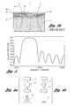
- FIG. 3is a graph of reflection as a function of wavelength of a multi-layer stack having 28 layers in 14 pairs, the stack representative of a device processed with a method and system of the present invention
- FIGS. 4 a and 4 bare top views and associated graphs which illustrate the effect of irradiating the target structure with laser beam profiles of varying dimension with respect to the target structure;
- FIGS. 4 a and 4 bshow the result of truncating a representative non-uniform Gaussian shaped laser spatial profile, wherein the energy enclosed by the target structure is strongly affected, the energy at the target edge varies, and potential stray radiation effects result from energy not absorbed by the target structure;
- FIG. 4 cis a side schematic view of a plurality of microstructures formed on a layer and which illustrate that for decreasing spacing (pitch) inter-reflections and stray energy result in irradiation of neighboring target structures;
- FIGS. 5 a and 5 bare graphs which show the reduction in irradiance on the device as a function of depth resulting from precise position control of a high numerical aperture beam (at the top surface), wherein the position and depth of focus of the beam provides for processing of the target structure without creating undesirable changes to other materials;
- FIG. 5 aillustrates the increase in spot area with for various spherical and elliptical Gaussian irradiance distributions, for a representative multi-layer stack used in a copper memory process;
- FIG. 5 bnormalizes the defocus function relative to the energy density (fluence) at the target location
- FIGS. 6 a and 6 bare schematic views of a stack of layers formed on a wafer substrate and which illustrate exemplary results obtained with a ray trace simulation used to estimate the level of radiation impinging on the internal layers and adjacent links with a specified beam numerical aperture;
- FIGS. 7 a , 7 b , 8 and 9are views of images taken from detectors and which illustrate, on a continuous scale spanning 5 decades, simulated patterns of radiation at the surface, substrate, and with the stack removed respectively;
- FIG. 10is a schematic diagram of a system for measuring fiducials or other alignment targets
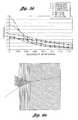
- FIG. 11is a graph of reflectivity versus outer layer thickness
- FIG. 12shows a pair of graphs of reflectivity versus thickness of the outer oxide layer for two different laser beam wavelengths
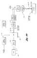
- FIG. 13is a schematic diagram of a system for automatically controlling pulse energy based on a thickness measurement
- FIG. 14 ashows schematic and graphical representations of an effect of debris on signal fidelity during alignment measurements
- FIG. 14 bshows similar representations with improved signal fidelity after cleaning with a pulsed laser beam
- FIGS. 15 a - 15 cshow various arrangements for combining laser pulses or generating a sequence of closely spaced pulses using optical or electronic delay methods;
- FIG. 15 aillustrates use of multiple lasers with delayed triggering;
- FIG. 15 billustrates a basic arrangement with a single laser and an optical delay path; and
- FIG. 15 cillustrates yet another modular optical delay line providing for pointing stability and simplified alignment;
- FIG. 16is a graph of temperature versus time which illustrates simulation results for metal link (top) and substrate (bottom) irradiance with a pair of delayed pulses wherein the substrate temperature decays rapidly exhibiting a differential thermal property of the materials; the two laser pulses each had a square temporal shape;
- FIG. 17is a series of schematic views of a metal link which illustrate a multiple pulse sequence wherein: (1) a first pulse irradiates the metal link; (2) debris is left after removing the link; (3) a second pulse with a spatial pulse shape is used wherein the central zone is attenuated, the second pulse having a lower peak energy density than the first pulse; and (4) 25 ns after the start of the first pulse the debris is removed;
- FIG. 18is a block diagram of a system which generates and controllably selects pulses
- FIG. 19is a block diagram of a system of the present invention wherein a portion of a high repetition rate pulse train (e.g., 1 ⁇ Hz) is selected and a high speed beam deflector (e.g., electro-optic or acousto-optic device) synchronized with microstructure positions is used to process a single microstructure with multiple pulses during relative motion; and
- a high repetition rate pulse traine.g., 1 ⁇ Hz
- a high speed beam deflectore.g., electro-optic or acousto-optic device
- FIG. 20is a block diagram of another system of the present invention wherein a beam deflector is used to spatially split a single pulse so as to irradiate either one or two microstructures (or none) with a pair of pulses during relative motion.
- a new fabrication processincludes a copper target structure, multiple dielectric layers in the form of a “stack,” and functional circuitry disposed at the dielectric layers.
- the target structure and layersare typically formed on a silicon substrate. This is illustrated in FIGS. 1 b and 1 c and corresponds to a device processed with an embodiment of the present invention. This will be referred to as a “multilevel” process.
- aspects of the inventioninclude methods and subsystems for operation of the laser processing system.
- the laser beam waistdiverges rapidly due to the small spot size and depth of focus.
- the materials within the 3D beam locationmay include functional circuitry.
- robust measurement of target locationsis used in conjunction with database information to position a laser beam in three dimensions at high speed.
- the interaction of a laser beam within the multilevel deviceinfluences yield. Modeling of thermal interaction is useful of understanding and predicting performance in the thermal processing regime.
- a more detailed understanding of interaction based on physical opticsis also beneficial.
- a pulsed laser beamthe beam having pre-determined characteristics for processing of microscopic structures, is used to cleanly remove at least a portion of a target structure.
- An application of the method and system of the present inventionis severing of highly reflective copper links which are part of a high speed semiconductor memory device.
- the method and system of the present inventionis particularly advantageous for processing of targets having a sub-micron dimension, including targets with a dimension below the wavelength of the laser beam.
- the targetis separated from a semiconductor substrate by a multi-layer stack, which may have several dielectric layers.
- both the temporal and spatial characteristics of the pulsemay be selected or controlled based on the thermal and optical properties of the microscopic target, underlying layer materials, and the three-dimensional layout of the device structure, including the spacing of target structures and functional inner conductor layers.
- FIGS. 1 a - 1 cgenerally show an embodiment of the present invention
- a laser pulse 3irradiates a rectangular target structure or microstructure 10 , side views of which are shown in FIGS. 1 b and 1 c , with a focused beam.
- an output from short pulse amplified laser system 1is generated to produce the pulse 3 which has a rise time 4 fast enough to efficiently couple energy into a highly reflective target structure.
- the duration 5is sufficient to process the target structure wherein at least a portion of the structure is cleanly removed without leaving residue, slag, or other debris.
- the fall time 6is preferably fast enough to avoid creating undesirable damage to the layers or substrate.
- the temporal pulse shapeis selected, in part, based on physical properties of the target microstructure 10 , for instance, thickness, optical absorption, thermal conductivity, or a combination thereof.
- the processingwill occur with a single pulse having a fast edge leading relative to a selected pulse duration of several nanoseconds.
- the laser outputmay be a series of narrow q-switched or rectangular pulses, with very fast rise time, for example 800 ps pulses representative of the output of commercially available q-switch micro-lasers.
- the pulsesmay be delayed with respect to each other so as to provide a burst of pulses to irradiate the target structure.
- the laser outputmay be generated with a combination of a high bandwidth seed laser diode and fiber optic amplifier with Raman shifting, or with a waveguide amplifier system.
- a desirable pulse characteristicmay be provided with various modified q-switched systems or with the use of high speed electro-optic modulators.
- Other pulse shapesmay be selected for the material processing requirements. For instance, a sequence of closely spaced pulses having duration from a few picoseconds to several nanoseconds is taught in Reference 5.
- a high bandwidth MOPA configurationis used to amplify the laser output of a high speed semiconductor diode.
- Generation of various pulse shapes and duration with direct modulation of the diodeis considered advantageous, provided any affect associated with variable amplitude drive waveforms does not affect overall performance. Further details of various aspects of pulse generation and amplification can be found in references 5 and 6 (e.g., in '471—Reference 5—FIGS. 5 and columns 14-16).
- embodiments of the laser systemmay include fiber optic amplifiers which amplify the preferred square pulse shape generated by a seed laser.
- the seed lasermay be a high speed semiconductor diode or the shaped output of a modified q-switched system.
- the amplified outputmay be matched in wavelength to the input or Raman-shifted as taught in References 4 and 6 (e.g., in Reference 6, FIGS. 12-13 and column 14, line 57—column 19, line 3). Wavelength shifting of a short pulse q-switched laser output is generally taught in '759 Reference 4.
- the seed laseris a semiconductor diode and the optical amplifier is a waveguide amplifier.
- Advantages of an embodiment with a waveguide amplifier when compared to a fiber systeminclude avoidance of Raman shifting, lower pulse distortion at the speed of operation, and, with proper design, minimal thermal lensing.
- a precision anamorphic optic systemis used to optimize coupling between the seed and amplifier. Basic description of waveguide amplitude and lasers can be found in product literature provided by Maxios, Inc. and in the article “CW and passively Q-switched Cladding Pumped Planar Waveguide Lasers,” Beach et. al.
- a plurality of q-switched micro-laserscan be used for generation of a fast rising pulse or other desirable shape.
- the modulesproduce a q-switched waveform with pulse durations of about 1 nanosecond or less, for example 800 ps to 2 ns for commercially available units.
- An example of a commercially available laseris the AOT-YVO-1Q available from Advanced Optical Technology (AOTLasers.com).
- AOTLasers.comAdvanced Optical Technology
- active q-switch laserscan be triggered with a TTL pulse at a variable repetition rate while maintaining specified sub-nanosecond timing jitter.
- the pulse shape incident on the target microstructurewill vary significantly at repetition rates approaching the maximum rate.
- Reference 9teaches methods of maintaining a constant pulse shape despite variations in the temporal spacing of pulses incident on a target (e.g., see the figures and associated specification).
- AOToffers a pulsewidth of 2 nanoseconds available at a repetition rate of 20 KHz. Frequency doubled versions are also available (532 nm).
- the q-switched waveformsmay approximate (at least to 1st order) a symmetric Gaussian shape, or a fast rising pulse with an exponential tail, depending on the stored energy.
- a series of deviceswith appropriate delays introduced by a plurality of triggering signals, or delays of a trigger signal with a delay line, is used to generate a series of spaced apart pulses.
- the optical outputsare preferably combined with appropriate bulk optics (polarization sensitive), fiber optics, or waveguides to form a single output beam.
- the resultant addition of the q-switched waveformsproduces a fast rise time characteristic and relatively short duration.
- An optical amplifier 122may be used to increase the output power as needed.
- FIG. 15 ashows a schematic of one basic embodiment with bulk optics, where a beam combiner 123 is used to deliver the output of two lasers 120 , 121 to an amplifier 122 .
- a delay circuit 126which may be programmable, controls triggering.
- Polarization optics 127 , 128are used to provide the proper input to the beam combiner.
- the pulsesare spaced apart and appear as a high frequency burst 124 .
- triggering of the second pulseoccurs at a slightly delayed (but controlled) position which produces a characteristic approximating a square pulse shape 125 .
- the controlled delayis about 50% of the FWHM.
- Generation of multiple pulse waveformsmay also include some form of active q-switching of two separate microlasers or detecting a first pulse from a passively q-switched laser and subsequently triggering an actively q-switched laser or MOPA relative to the first pulse.
- FIG. 15- bis a basic schematic showing the use of a single laser 140 wherein the laser output is divided by beam splitter 142 , whereby a portion of the beam propagates along a path 141 , followed by combining with combiner 143 , after polarization adjustment with rotator 146 which may be a half-wave plate.
- An optional optical amplifier 145may then be used to produce higher output power.
- FIG. 15 cshows an exemplary embodiment wherein the use of opposing corner cube retroreflectors 130 makes the setup insensitive to tilt of the folding elements.
- the angular alignment of the delayed beam paths 131 , 132is very stable even in a high vibration environment.
- One of the corner cubes in each pair of retroreflectors 130is initially adjusted in the X/Y translation and Z rotation to get the transverse position of the delayed beam path centered.
- Each of the ⁇ /2 retarders 133 in the main beam pathis adjusted so that vertical or horizontally polarized light will have its polarization rotated by 45 degrees.
- the ⁇ /2 retarder 133 in the second delay loopis adjusted so that vertical or horizontal polarized light will have the polarization rotated by 90 degrees causing the delayed pulse in the second loop to circulate twice before exiting.
- the peak-to-peak spacing of the output waveform 135e.g., 4 combined pulses
- the ⁇ /2 retarders 133 in the main beamcan be set for a polarization of other than 45 degrees.
- the pulse shapecan be varied at the time a system is setup or possibly in operation by manually or automatically controlling the spacing.
- Another means of producing a shaped pulseis to use the modulator approach to chop the leading edge or tail of the pulse but with a two-stage or shaped modulation voltage pulse. For example: with a 10 ns q-switched pulse, the modulator could have 100% transmission for the first 1-5ns followed by 25% transmission for the remainder of the pulse.
- Early pioneering work by Koechner (U.S. Pat. No. 3,747,019) and Smart (U.S. Pat. No. 4,483,005)demonstrate exemplary amplitude and pulse shape control methods using electro-optic modulators.
- the multiple pulses shown in FIGS. 15 a - 15 cmay or may not have the same wavelength, and the temporal shape of a pulse may be varied depending upon specific requirements.
- an outputmay be a q-switched pulse of short duration and high peak power combined with a lower power square pulse shape.
- position informationobtained with a precision measurement system, is used to relatively position the focused beam waist of the pulsed laser at a location in space 7 , 8 , 9 to substantially coincide with the target 10 three-dimensional coordinates (Xlink, Ylink, Zlink).
- a trigger pulse 2generated at a time where the laser beam waist and target position substantially coincide, operates in conjunction with the laser and associated control circuitry in laser subsystem 1 to produce an output pulse.
- References 2 and 7describe details of a method and system for precision positioning, including three-dimensional beam waist positioning.
- Reference 7describes a preferred embodiment for producing an approximate diffraction limited spot size with a range of spot size adjustment (e.g., FIGS. 7-9 of WO0187534 ('534) and the associated specification), and a preferred method and system for three-dimensional positioning of the beam waist.
- Three-dimensional (height) informationis obtained, for instance with focus detection, and used to estimate a surface and generate a trajectory (e.g., FIGS. 2-5 of '534 and the associated specification).
- the laseris pulsed at a location substantially corresponding to the three-dimensional position of the link (Xlink, Ylink, Zlink) (e.g., FIGS. 10 a-b of '534 and the associated specification).
- the three-dimensional measurement and positioningare used to compensate for topographical variations over a wafer surface, or other position variations introduced in a system (mis-alignment). These variations are generally system or application dependent and may exceed several microns, which in turn exceeds the depth of focus of the focused laser beam. In some micro-machining applications the system positioning requirements may be relaxed if certain tolerances are maintained, or if external hardware manipulates the device position, as might be done with a micro-positioning sub-system.
- the devicemay comprise a miniature part (e.g., single die) which is positioned by an external micro-positioning subsystem to a predetermined reference location.
- the positioningmay be based on single measurement at a reference location or perhaps a single depth measurement combined with a lateral (X, Y) measurement.
- a lateral (X, Y) measurementFor processing of multilevel devices on wafers, (e.g.: 300 mm) at high speed it is expected that densely sampled three-dimensional information will improve performance, particularly as link dimensions shrink.
- an alternative methodis to combine information which may be predetermined (e.g., the plane of a wafer chuck relative to a beam positioner plane of motion measured during a calibration process) with dimensional information obtained from each part to be processed. For example, in '534, FIGS. 1-2 , a fraction of the tilt of region 28 may be associated with fixturing).
- the stepsmay include (a) obtaining information identifying microstructures designated for removal, (b) measuring a first set of reference locations to obtain three-dimensional reference data, (c) generating a trajectory based on at least the three-dimensional reference data to obtain a prediction of beam waist and microstructure surface locations, (d) updating the prediction during relative motion based on updated position information, the updated position information obtained from a position sensor (e.g., encoder) and/or from data acquired during the relative motion.
- the additional datamay be measurement data acquired at additional alignment target or at other locations suitable for an optical measurement (e.g., dynamic focus).
- Reference 2describes a system wherein a precision wafer stage is used to position a wafer at high speed.
- FIGS. 9-11 and columns 5-6 of Reference 2describe aspects of the precision measurement subsystem associated with the precision positioning apparatus. Additionally, designated reference locations on the workpiece (e.g., wafer) which may be an x, y alignment target or a region suited for a three-dimensional measurement may be used for various applications. It should also be noted that height accuracy of about 0.1 ⁇ m was reported in “In-situ height correction for laser scanning of semiconductor wafers,” Nikoonhad et al., Optical Engineering, Vol. 34, No.
- an optical position sensorobtained area averaged height data at high speeds.
- a dynamic focus sensore.g., astigmatic systems used for optical disk tracking and control
- the data rateis fast enough to support “on the fly” measurement.
- a combinationmay be based on the number and typical distribution over a device of microstructures designated for removal. When a large number of repair sites are distributed across a device, the throughput may be maximized by providing updates “on the fly.”
- the target structure 10is provided as a part of a multi-material, multi-layer structure (e.g., redundant memory device).
- the multi-layer stack having dielectric layers 14 , 15provides spacing between the link and an underlying substrate 17 .
- alternating layers of Silicon Dioxide 15 and Silicon Nitride 14may be disposed between a copper link target structure 10 and a Silicon substrate 17 .
- the copper target structureis generally located in proximity to other similar structures to form a 1-D or 2-D array of fuses which are designated for removal.
- underlying conductors 16 disposed as part of the functional device circuitrymay be in proximity to the link structure, and arranged in a series of patterns covered by relatively thin ( ⁇ 0.1 ⁇ m typical) Silicon Nitride 14 and thicker ( ⁇ 1 ⁇ m typical) Silicon Dioxide 15 materials.
- the irradiance distribution at the linkmay substantially conform to a diffraction limited, circular Gaussian profile.
- the beamhas an approximate elliptical Gaussian irradiance profile, as might be produced with an anamorphic optical system, or with a non-circular laser output beam.
- the incident beamhas a non-uniform aspect ratio 12, 11 as also illustrated in FIG. 4 b (e.g., 3:1).
- rectangular or another chosen spatial profilesmay be implemented in a lateral dimension.
- Reference 1discloses various advantageous methods and optical systems for “non-Gaussian” spatially shaping of laser beams for application to memory repair.
- the preferable minimum beam waist dimension at location 11approximates the narrow target 10 dimension of FIG. 1 b , which, in turn, produces high pulse energy density at the link. Further, with this approach, a high fraction of the laser energy is coupled to the link and background irradiance is reduced.
- a typical copper link used in a present memoryhas width and thickness of about 1 ⁇ m or less, for example, 0.6 ⁇ m, and length of about five microns. Future memory requirements are expected to further reduce the scale of target dimensions.
- the minimum beam waist dimension Wyo at 11will typically overfill the sub-micron link to some degree, whereas aspect ratio Wxo/Wyo 12, 11 with Wxo a few microns along the link, can facilitate clean link removal. Additionally, rapidly decreasing energy density on the layers 14 , 15 and substrate 17 is achieved through defocus of the high numerical aperture beam portion 11 .
- FIGS. 5 a and 5 billustrate the estimated defocus for various aspect ratios, relative to a circular Gaussian and an elliptical beam at best focus.
- FIG. 5 ashows the very rapid falloff of a 1.6 ⁇ m circular Gaussian (0.002 mm numerical divisions ⁇ 2 ⁇ m).
- FIG. 5 bshows a normalized result to scale the energy density at best focus for the different spot shapes.
- copper link removalis initiated with application of the fast rise time pulse, having a nominal 10-90% rise time 4 in a preferred range of less than 1 nanosecond to about 2 nanoseconds.
- a pulse duration 5 in the range of about 2 nanoseconds to 10 nanosecondsis preferable to sever the link while limiting thermal diffusion.
- Pulse energies in the range of about 0.1 microjoules ( ⁇ j) to 3 ⁇ jwere effective, with a preferred typical range of about 0.1-5 ⁇ j considered sufficient margin for spot shape and process variations.
- the preferred pulse durationmay be selected based upon the nominal link thickness specifications, or based on a model of the dissimilar thermal and optical properties of adjacent materials.
- a combination of the spatial characteristics (e.g., beam waist shape and position) and the temporal (e.g., rise time 4 , flatness, and duration 5 ) pulse characteristicsavoids undesirable cracking of lower layers 14 , 15 , avoids significant pulse interaction with inner layer conductor 16 , and limits substrate 17 heating.
- the target structureis processed without undesirable damage to other structures.
- copperin addition to having nearly maximum reflectance in the near IR, is also more reflective than other link materials (e.g., aluminum, platinum). Nevertheless, due to the optical interaction of the near IR beam with the target and the optical and thermal properties of adjacent (overlying) layers, the preferred copper material can be processed.
- near IR (Infrared) wavelengthsalso conveniently correspond to wavelengths where high bandwidth laser diodes are available, and to the spectral range where optical amplification of the pulsed laser beam can be efficiently produced with fiber and waveguide amplifiers.
- amplified laser diode outputshaving a desired temporal pulse shape, may also be frequency multiplied to produce visible laser outputs when advantageous.
- the fast rise time of semiconductor diodesis particularly advantageous for producing a fast rise time, square pulse characteristic. Future developments in visible diode and optical amplifier technology may support direct pulse amplification in the visible range.
- the link widthis a fraction of one micron and the link spacing (pitch) is a few microns with present process technology.
- the link widthmay typically correspond to a wavelength of visible light.
- the thickness and indices of refraction of the stack materialscan significantly affect the overall optical characteristics of the stack.
- a preferred reduced wavelengthis selected in the visible or near infrared range wherein a non-absorptive optical property of the layers (e.g., interference or reflection loss) is exploited.
- the device structure of FIGS. 1 a and 1 bcan be damaged with substantial absorption within the lower layers, such damage is prohibitive because of the presence of adjacent circuitry. This is in contrast to link processing with the prior art system of FIG. 2 b where inner layer damage is not generally detrimental to overall device performance.
- U.S. Pat. No. 6,300,690(Reference 8) describes a system and method for vaporizing a target structure on a substrate.
- the methodincludes providing a laser system configured to produce a laser output at the wavelength below an absorption edge of the substrate.
- Reference 4discloses benefits of a wavelength less than 1.2 ⁇ m for processing links on memory devices wherein the substrate is Silicon, namely smaller spot size and shorter laser pulsewidths.
- improved performancecan be realized by exploiting the non-absorbing stack properties with wavelength selection.
- at least one of precision positioning of a high numerical aperture beam, spatial shaping of the spot, or temporal pulse shapingalso will provide for reduced energy at the substrate. The result corresponds to a relatively low value of energy expected to be deposited in the substrate, despite an incident beam energy necessary to deposit unit energy in the target structure sufficient to vaporize the target structure.
- the factors affecting the energy deposited in the substrateare, in effect, multiplicative.
- copperis absorbing (e.g., about 50% at 500 nm, 70% in the near UV, compared to 2% at 1.064 um) so less energy is required for clean removal, at least an order of magnitude.
- the preferred identified wavelength corresponding to a relatively low value of the energy expected to be deposited in the substrateis within a visible of near IR region of the spectrum.
- a model-based approachmay be used to estimate the shortest wavelength with sufficient margin for a specified dielectric stack, spot position, tolerance, temporal and three-dimensional spatial pulse characteristics.
- the limiting wavelength corresponding to a relatively low value of the energy expected to be deposited in the substratemay be within the green or near UV region of spectrum, but the use may require tightly controlled system parameters, including possible control of the stack layer thickness or index of refraction.
- wavelength selectionin accordance with the present invention, where the internal transmission and preferably reflection of the stack is at or near a maximum, stack layer damage is avoided. Furthermore, decreasing substrate irradiance, while simultaneously providing a reduced spot size for link removal (at or near diffraction limit), is preferred provided irradiation of functional internal layers is within acceptable limits.
- Spectral transmission curves for typical large bandgap dielectric materialsgenerally show that the transmission decreases somewhat at UV wavelengths.
- the transmission range of Silicon Dioxideis specified as wavelengths greater than 0.15 ⁇ m. The absorption coefficient of both Silicon Nitride and Silicon Dioxide remains relatively low in the visible range (>400 nm) and gradually increases in the UV range.
- FIG. 3is a graph which illustrates the estimated back reflection produced by a representative multi-layer stack of 14 Silicon Dioxide 15 and Silicon Nitride 14 pairs over a range of near IR wavelengths, where the thickness of the layers is about 1 ⁇ m and 0.07 microns, respectively.
- a large number of layerscan be accommodated, and may range from about 4-28 dependent upon the process (e.g., sometimes multiple layers may separate a functional conductor layer).
- exploiting the layer reflection with wavelengthcan further enhance the system performance and supplement the benefits associated with temporal and spatial control of the pulse in a preferred short wavelength range.
- Such wavelength selectionis regarded as particularly advantageous at wavelengths where the substrate absorption would otherwise greatly increase, and significant margin can be obtained when the number of layers 14 , 15 disposed between the link and substrate substantially exceeds the number of overlying layers 13 .
- a preferred structure for processingwill comprise a substantial number of layers, with large reflectance at a predetermined short wavelength, the wavelength being well matched for generation of the preferred fast square temporal pulse shape.
- Standard laser wavelengths in the range of FIG. 3include 1.047 ⁇ m and 1.064 ⁇ m, the latter being a standard wavelength of semiconductor diodes. Further, custom wavelengths include 1.08 ⁇ m, and other wavelengths generated with Raman shifting.
- frequency multiplication of the near IR wavelengthscan be used to generate short wavelengths, and with appropriate design multiple wavelengths may be provided in a single system. For instance a preferred temporal pulse shape, with a fast rise time, may be generated in the green portion of the visible spectrum by frequency doubling a near IR laser.
- wavelength tuningis used to match the wavelength to the approximate peak reflectance of the stack.
- Such an arrangementmay be particularly advantageous for adjustment of a laser wavelength at the edge of the reflectance range (i.e., “cutoff” range) over a limited wavelength range, whereby sensitivity to tolerances in the material thickness and index of refraction are avoided.
- Generation of the pulsed laser beammay include the step of shifting the wavelength of the laser beam from a first wavelength to a predetermined wavelength.
- the predetermined wavelengthmay be based on material characteristics comprising at least one of: (1) coupling characteristics of the microstructure, (2) multi-layer interference, and (3) substrate reflectivity.
- a specification for a multi-layer stackmay be considered in process design.
- a quarter-wave stack of alternating dielectrics or other suitable arrangement having a large difference in the index of refraction, and high transmission within each layeris specified at a selected wavelength. It can be shown that very high reflectance is achievable, the quarter-wave stack being easily computed in closed form and modeled.
- the method and system of the present inventioncan be used effectively with other aspects of process design, and may be advantageous where the absorption of deeply buried layers and the substrate is relatively high, or where the width of a target structure is well below the laser wavelength.
- the design of the device structuremay have certain constraints related to the layout of the circuitry.
- certain thickness and material for a certain layermay be defined, for instance an insulator in a plane of a conductor having the approximate thickness of the conductor, or related to the thickness of the conductor. It may be possible to select a material having a different index of refraction than the specified layer.
- a specified thicknessmay be based on the estimated reflection at an advantageous laser wavelength which may reduce or eliminate a requirement for special laser equipment operating at “exotic” wavelengths where the lasers are difficult to manufacture with high yield.
- the reflectionmay be estimated using a model wherein the thickness is a variable, and an estimate made to maximize the reflection, subject to other device constraints.
- Thickness of the layerscan be tuned to a wavelength in as much as the wavelength (or angle) can be tuned to the layers.
- Index of refractioncould be used to fine-tune over a limited range, but the range may not be significant for small changes in index.
- a variable thickness tuning layer or layers with predetermined thicknesscould be used to significantly affect reflectivity of the whole stack.
- a layer not constrained by metallization requirementscould be used as a precision spacer between an upper and a lower stack portion. This could be a very powerful tool for tuning the process with adjustment of perhaps only one layer.
- Reference 3describes an advantageous method and system for polarization control, including dynamic polarization selection and computer control so as to align the polarization with a link orientation (e.g., details shown in FIG. 4 and the associated description in the reference).
- the polarizationcan be selected on the basis of the target coupling characteristics, the film reflectance, or a combination thereof.
- FIGS. 4 a - 4 cillustrate effects of reflection and diffraction associated with sub-micron width link 10 resulting in truncated 43 , 44 Gaussian beams 11 , where the spot size (as measured at the 13.5% point) is wider than the link by varying degrees.
- the sketchesare representative of a diffraction limited beam waist at a near IR wavelengths.
- the central lobeis clipped by the link, which appears as a near field obscuration, resulting in transmitted beam portions which are truncated 43 , 44 .
- Energy which is not incident on the linkmay propagate at wide angles into the layers 49 which may be advantageous from the standpoint of avoiding damage to the substrate 17 as shown in FIG. 1 .
- FIGS. 6 a and 6 billustrate by way of example geometric ray tracing effects of internal reflections propagating over an extended area.
- the energy which is not coupled into the link structuremay also be scattered and/or specularly reflected to the adjacent links 48 .
- the inter-reflection 47occurs as a consequence of at least the link 46 physical edge profiles which may be slightly curved or sloped.
- FIG. 4 cAn additional consideration is the three-dimensional spacing between an inner conductor layer 16 of FIG. 1 , the beam waist 11 , and the adjacent links 48 of FIG. 4 c .
- a large numerical aperture beam waist 11producing the smallest spot size at the link, while diverging and reflecting in a manner so as to avoid significant interaction with the inner layer 16 is preferred.
- FIGS. 4 a - 4 csuggest a reduced spot size with controlled precision 3D waist positioning is expected to reduce collateral damage by maximizing energy coupled into the link. With high enclosed energy within the link and a low intensity transmitted profile 44 , edge reflection is minimized.
- the spatial profileshould also be selected subject to the constraint of only low level, negligible interaction between the beam angular distribution at 16 .
- the interaction mechanisms associated with a portion of the three-dimensional device structurebe modeled for selection of at least a spatial pulse characteristic, such a characteristic may be the N.A. and position of the beam waist.
- the modelwill include an estimate of the irradiance seen by each adjacent link structures 48 , internal layer 16 , and substrate 17 . Whereas damage to adjacent link structures may be relatively apparent with conventional microscopy, assessment of inner layer 16 and substrate 17 damage may be considerably more difficult with the 3-D device structure.
- a precision positioning method and systemis used to relatively position the beam waist so as to provide high laser energy concentration at the link. Also, one important consideration for precision positioning is predicting accurate (Xlink, Ylink) location information. The prediction is subsequently used by a motion control and positioning system to generate a laser output via trigger 2 at the target coordinates, during relative motion of the target 10 and laser beam.
- a preferred embodimentincludes a polarization insensitive scanning and detection system as described hereinbelow, wherein a region containing an alignment target location is imaged to obtain reference data.
- the target locationis often covered by a dielectric layer of Silicon Dioxide, Silicon Nitride, or other insulating material.
- polarization insensitive detectionis advantageous to avoid spurious measurements.
- the resultsled to a hypothesis that that birefringence is introduced in the insulating layers by polishing or other process operations, which is manifested by polarization variations in the reflected beam. These variations reduce the signal-to-noise ratio and appear to induce position distortion.
- the digital output data from each target locationis used by an 8-parameter least squares alignment algorithm to estimate and correct position information affected by offset, angle, scale, orthogonality, and trapezoidal variations over the wafer containing the links to be processed.
- a model-based approachleads to selection and precision control of the spatial and temporal characteristics of the laser output, resulting in controlled three-dimensional interaction of the laser with complex multi-layer, multi-material structures.
- the reflectance/transmission (R/T) split of the beamsplitter 150depends on the laser that is being used. In cases where the laser has low total energy and as much transmission as needed is necessary, the split of 90% transmission and 10% reflectance is made. This gives 90% going to the work surface on the way in and the 10% reflected is dumped. But this only picks off 10% of the reflected light, 90% of the reflected light is transmitted back down the laser path. When possible, the split 70/30 is made. This gives less total energy to the work surface but gives higher reflected signal.
- R/Treflectance/transmission
- the method and system of the present inventionare advantageous when there are oxide layers over the targets to be scanned and measured.
- the oxide layermay affect the polarization of the beam. This may happen because the oxide layer is stressed and creates birefringence. With, the polarization insensitive arrangement this is not a problem, no matter how the polarization is changed one gets the same reflectance from the beamsplitter and the same signal level. If a more typical polarizing beamsplitter or simpler coating is used for the beamsplitter, the changed polarization will result in a change in the reflected signal. If the stress in the oxide layer varies, especially where it is over the target microstructure (it may be stressed because it is going over a target edge) then the polarization may vary as the beam scans the target.
- the coatingIn the polarizing beamsplitter case the reflected signal 151 measured at the detector would vary because the polarization is varying at the same time that one is trying to gather edge data, skewing the results uncontrollably and unpredictably.
- This polarization insensitive techniqueis regarded as the most robust method and is preferred for measuring targets covered by at least one oxide layer.
- other imaging and edge location methodsmay be used, but may require more complex measurement algorithms to accurately measure the targets in the presence of multiplicative image noise.
- a typical alignment target 100is depicted in the schematic drawings of FIGS. 14 a and 14 b .
- the target 100is typically covered with one or more passivation layers, these may correspond to the layer 13 in FIGS. 1 b and 1 c , but are not so restricted.
- the preferred polarization insensitive measurement methodwas used to obtain X, Y target locations.
- debris 1001 within the target area 100possibly from residual solder flux from nearby solder deposits (solder balls), significantly affected the reflected signals obtained with a detector resulting in noisy profiles 101 .
- the impact on the measurementwas manifested as a large residual in the least squares fit algorithm used to estimate location.
- the target areais shown as a positive contrast (e.g., higher measured intensity) region, but those skilled in the art will recognize that contrast reversal is acceptable provided that the contrast between the target 100 and the background is adequate for measurement.
- a pulsed beam with lower peak powerwas used to remove the debris.
- An enhanced exemplary signal profile 102(e.g., associated with relatively uniform intensity and a mostly debris-fee region) was obtained as a result of the cleaning operation, as shown in FIG. 14 b .
- Representative energies for cleaningwere on the order of 0.01 ⁇ j, for instance, 0.005 ⁇ j. This is well below the damage threshold of the materials, and well below the typical energies used for removal of links 12 .
- a single linear scan or a plurality of linear scans 104 across the target 100are used to obtain reflected intensity data which is analyzed statistically to measure fidelity, for instance by determining the % intensity variation or standard deviation.
- datais taken along the line(s) 104 at about every 0.001′′.
- the sample spacemay be finer or coarser depending upon the signal fidelity obtained. If the spacing is too fine, additional “texture noise” may be introduced. If too coarse, an edge contrast 107 will be reduced or errors introduced by undersampling. If the variation is excessive, a cleaning operation is initiated with a pulsed beam.
- the laser poweris controlled with an acousto-optic modulator (i.e., “energy control” of FIG. 13 ) which is a standard part of the laser processing equipment.
- an acousto-optic modulatori.e., “energy control” of FIG. 13
- the operation of the modulator for intensity control and pulse selection within a link blowing systemis described in more detail in U.S. Pat. No. 5,998,759 (e.g., Reference 4, col. 7, and the associated drawings).
- modulatorsprovide for intensity control over a wide dynamic range, e.g., 100:1.
- a relatively simple user interfacecan provide for operator interaction to initiate operation, based on “pass/fail” or other criteria.
- the linear scan(s)may be done automatically and the cleaning operation performed at each measurement location.
- the cleaning operationwill be applied only to scanned regions as needed.
- the processis iterative with a measurement goal of obtaining suitable residuals in the least squares fit algorithm. If the residuals are above a designated value, scans of at least one region are obtained and cleaning occurs. In some cases, it may be desirable to adjust the positions of the scan lines (e.g., if cleaning is difficult).
- a fidelity measuremente.g., contrast, standard deviation
- the above discussionrelated to a preferred measurement method and system for locating and measuring X, Y reference locations.
- An additional option to further improve the process energy windowis measurement and control concept to adjust the laser energy and power as required by the material to be processed. If the reflectivity is high, then the energy is to be increased to compensate for these reflection losses. If the reflection is low, then the energy and power is to be decreased since more energy is being coupled into the workpiece or target microstructure. There are a number of ways that one can adjust this power and energy. The simplest is to measure the reflectance from the surface and adjust the energy and power control for optimum energy coupling.
- the thickness of a layermay vary by 10% and there may be several layers of oxide between the top layer and the metal layer to be processed.
- the energy required to process the linkcould be calculated and adjusted accordingly.
- Another methodis to measure the reflectance at two different wavelengths and calculate the thickness of the oxide. If the index of refraction of the oxide used for the device could be measured, then the reflectance and hence the fraction of the laser radiation absorbed over the link can be calculated. Knowing this absorption, the optimum laser energy to remove the link can be programmed into the laser system. This second method is more accurate for thin film trimming where the material to be trimmed is thin and some of the energy is transmitted through the film.
- the implementation of the thickness measurement and energy controlis as shown in FIG. 13 .
- the laser 160 used to remove the linkprovides one of the laser wavelengths for the thickness measurement.
- the energy delivered to the partis controlled by an acousto-optical modulator (i.e., “energy control”) 161 as shown in FIG. 13 and is reduced to a level to measure the reflectance without damaging the part.
- the other wavelength to measure the reflectivitycan be provided by a red laser diode (i.e., 670 mn diode) 162 added into the optical path as shown.
- Beamsplitters 166 , 167are generally used to transmit the two wavelengths to the device surface and to direct the reflected beams to the photodiode detectors 164 , 165 .
- the reflectancecan be monitored by the two photodiodes 164 , 165 as shown in FIG. 13 . From the reflectance intensity of the two photodiodes (i.e., the 670 nm diode and 1047 nm detectors) and knowing the index of refraction of the oxide layers, the thickness of the oxide is uniquely determined. Once the thickness and the index of refraction is known, then the absorption in the link material can be calculated and the optimum energy programmed into the acousto-optic energy control device by the computer.
- the size of the spot and the link dimensionscan be used in the calculation. Referring to FIGS. 4 a and 4 b , one sees that there is some energy that will fall off the link and therefore the difference in the reflected light that does not fall on the link has to be calculated. Hence, two measurements have to be made to accommodate for the reflected energy that is not covered by the link. These measurements can be made on each die if required and the energy per pulse can be varied as the thickness of the oxide varies across the wafer. Alternatively, the method could be selectively applied on a wafer-by-wafer basis for process monitoring, for instance. This technique will reduce the requirement to use a laser processing energy that is on the high side to account for the variations in absorption in the link due to interference effects.
- the process energy windowmay be improved in certain cases by adjusting the wavelength over a range wherein the coupling of energy to the target is improved, the stack reflectance is increased by way of the interference effect, or where the substrate reflectivity increases.
- Special solid state tunable lasersOptical Parametric Oscillators (OPO), Raman, or other tunable lasers may be used provided that power and repetition rate requirements are met for a given application.
- OPOOptical Parametric Oscillators
- RamanRaman
- other tunable lasersmay be used provided that power and repetition rate requirements are met for a given application.
- parametric oscillatorsmay be used which are of fixed wavelengths, that use 2 or 3 crystals at the same time. Under certain circumstances, tunable lasers are operable.
- 2001-0036206describes a tunable laser diode having a 40 nm range developed for the telecommunications industry (i.e. 1.55 ⁇ m wavelength).
- Standard OPO lasersprovide for high power and narrow pulses but generally a very slow rep rate, but may be suitable for certain applications.
- 10 KHz versionshave been demonstrated and proposed for 20 KHz repetition rates.
- U.S. Pat. Nos. 6,334,011 and 5,998,759 (Reference 4), and U.S. Pat. No. 6,340,806 (Reference 6)disclose various combinations of shifters.
- Fosterite lasershave a tunable region that essentially straddles the absorption edge region of silicon, and can permit operation both beyond and below the absorption edge of silicon. At the present state of the art, they do not appear to be as efficient as they may become in time. As materials and improvements are being continually developed in the laser field, it is within the invention to use such devices and obtain corresponding benefits for processing. For instance, the multilayer thickness and reflectivity measurements may be extended to select a wavelength range which will provide for an improved energy window.
- the above teachingscan also be selectively applied to conventional link structures (see FIG. 2 -B), for instance processing of high reflectivity copper links separated from the substrate by a single layer dielectric layer.
- Production trendsare pushing away from polysilicon structures and toward metal structures of Al and Cu, which poses on-going challenges for link processing systems to avoid reliability problems and to increase yield.
- many Cu-based deviceshave a multi-layer stack wherein substrate and stack damage can be avoided with wavelength selection, spatial beam shaping, or temporal shaping in accordance with the above teachings.
- some manufacturersetch all the dielectrics under the copper link and build the fuse on a single layer dielectric, with no SiN layers between the link and substrate. With conventional laser processing, the likelihood of substrate damages increases due to the high power required for Cu processing.
- double blastprocessing with multiple pulses
- there is generally a throughput problem for the double blast approachbecause two passes are required in present on-line memory processing systems.
- Simulated results and experimentsindicate a second blast may open the link completely even if 1st blast failed, despite extended time between first and second blasts. In specific cases improved yield was reported.
- double blast with 50% energy of a single blast energywas very interesting; it was observed that the Si substrate acts as a heat sink and cools down very fast.
- the copper target 202 recoverywas much slower indicating a significant differential thermal property.
- the second pulsewill also clear debris at cut site resulting in an “open circuit”. It is estimated that about 60-70% of the energy used in a “single blast” is needed for each pulse of “double blast.”
- the pulse energymay be varied with each pulse. In this example, the pulse delay was 50 ns, but it is clear that a much shorter delay may be possible.
- a delay line arrangement of FIG. 15 amay be used to avoid any delay in throughput.
- a preferred positioning system of the '118 patenti.e., Reference 2
- an optical delay lineFIGS. 15 b and 15 c , for instance
- 9 meters of extended path in air for the beamwill delay 30 ns for the second pulse.
- a second lasercould be used with a 30 ns or other controllable delay between the trigger pulses, and the trigger delay may be generated with a programmable digital delay line.
- the temporal pulse shapemay be a fast rising, square pulse (as was used in the simulation) generated with a seed laser diode, for instance.
- At least one pulsemay have a duration of greater than a few picoseconds to several nanoseconds.
- the pulsesmay be amplified mode locked pulses.
- At least one pulsemay generated with a q-switched microlaser having a pulsewidth less than 5 nanoseconds.
- At least one pulsemay propagate along a second optical path whereby the pulse delay is determined by a difference in optical path length as shown in FIGS. 15 b, c.
- Multiple laser and/or amplifiersmay be used as shown in FIG. 15 a.
- the generated pulses 275may have a repetition rate and a corresponding temporal spacing approximately equal to or shorter than a pre-determined delay (e.g., 60 MHz mode locked system) and a modulator is used to select the at least second pulse irradiating the microstructure or groups of pulses 276 .
- a pre-determined delaye.g. 60 MHz mode locked system
- U.S. Pat. No. 5,998,759e.g., Reference 4, col. 7, and the associated drawings
- an electro-optic modulatoris preferred.
- Additional opticsmay be used to spatially shape at least one of the delayed pulses, prior to combining for instance.
- a first pulse 210may be an elliptical or circular Gaussian spatial shape, or a top hat along the length of the link.
- the second pulse 212may have a different aspect ratio, or may be a special form of a “cleaning pulse” wherein the central zone of the spot is attenuated with an apodizing filter or effectively removed with a central obscuration. In such a case, the energy will be concentrated at the link periphery to remove debris 211 around the link location resulting from processing with the first pulse, thereby completing the processing 213 .
- Reference 1provides at least one example of beam shaping for link blowing applications, wherein a uniform distribution rather than Gaussian spot profile is disclosed.
- the relative motion between the microstructure and the laser beammay be significant between the pulses, e.g., greater than 25% of the spot size. This may be the result of a slower repetition rate (with increased pulse energy), faster motion speed, a longer pre-determined delay, or decreased target area.
- a slower repetition ratewith increased pulse energy
- faster motion speede.g., faster motion speed
- a longer pre-determined delaye.g., longer pre-determined delay
- a high speed, small angle beam deflectormay be used to compensate for the motion and deflect a delayed pulse to substantially irradiate the first microstructure at the slower repetition rate during relative motion 258 .
- the deflectorwould be operatively coupled to the relative positioning system controller 251 in a closed loop arrangement.
- the deflectoris preferably solid state and may be a single axis acousto-optic device which has a very fast “retrace”/access time.
- a higher speed electro-optic deflectore.g., a gradient index reflector or possibly a digital light deflector
- the time-bandwidth product(number of spots) can be traded for response time on an application basis.
- the deflectorwould preferably be used for intensity control and pulse gating/selection, as taught in Reference 4 (col. 7, and associated drawings).
- an electro-optic modulatormay be used with a separate acousto-optic deflector operated in a “chirp mode” 252 (e.g., linear sweep as opposed to random access mode) and synchronized (triggered) 253 based on the positioning system coordinates 254.
- the positioning system coordinatesare, in turn, related to the time at which the laser pulses are gated by the modulator to irradiate the same single microstructure 256 at times t 1 , t 2 , t 3 corresponding to the selected pulses 259 during relative motion 258 .
- a single laser pulseis used to blast up to two links at one time (e.g., no, one or two links).
- two focused spots 306 , 307are formed on two links by spatially splitting the single collimated laser beam 310 into two diverging collimated beams 309 .
- the use of acousto-optic devices for spatially splitting beams in material processing applicationsis known in the art.
- patent abstract JP 53152662shows one arrangement for drilling microscopic holes using a multi-frequency deflector having selectable frequencies f 1 . . . f n .
- a laser 300is pulsed at a predetermined repetition rate.
- the laser beamgoes through relay optics 302 that forms an intermediate image of the laser beam waist into the acoustic optic modulator (AOM) aperture.
- the AOM 303which operates in the Bragg regime, preferably is used to controllably generate the two slightly diverging collimated first order diffraction laser beams and control the energy in each beam.
- the angle between the two beamsis approximately equal to the Bragg angle for f 0 multiplied by 2( ⁇ f/f 0 ).
- the AOMcontrols the energy in each of the laser beams by modulating the signal amplitudes of two frequency components, f 1 and f 2 , in the RF signal and making adjustments for beam cross-coupling.
- the beamsAfter exiting the AOM, the beams go through the beam rotation control module 313 to rotate the beam 90 degrees on axis with links orientated in either the X or Y.
- a prismis used for this rotation, though many rotation techniques are well known as described in the regular U.S. application noted in the Cross-Reference to Related Applications section.
- the beamgoes through a set of optics to position the beam waist and set the beam size to be appropriate for the zoom optics and the objective lens 305 .
- the zoom opticsalso modify the angle between the two beams, therefore the angle between the two beams exiting the AOM has to be adjusted depending on the zoom setting to result in the desired spot separation at the focal plane.
- the laser beamsenter the objective lens 305 which provides a pair of focused spots 306 , 307 on two links. The two spots are separated by a distance that is approximately equal to the focal length of the lens times the angle between the two beams.
- a 80 MHz AOM center frequency with a sweep range of about 2.3 MHzmay be used to produce a spot size of about 1.8 ⁇ m on a pair of adjacent links spaced apart by about 3 ⁇ m.
- these linksmay have a dimension on the order of a laser wavelength (e.g., 1 micron) which, at very high speed operation, require the precision positions of the laser beam and microstructure.
- one aspect of the inventionis a method of selective material processing of a microscopic target structure with a pulsed laser beam.
- the target structureis separated from a substrate by a plurality of layers which form a multi-layer stack.
- the target structure, layers, and substratehave dissimilar thermal and optical properties.
- the methodincludes generating a pulsed laser beam with an energy density; irradiating the target structure with at least one pulse. Undesirable changes to the stack structure and substrate are avoided by selection of at least one pulse characteristic.
- a portion of the stackmay be irradiated with the laser beam during the processing of the target structure, yet undesirable damage to the layers, substrate, and functional circuitry in a plane of the inner layers is avoided.
- Undesirable damage of the stack structureincludes cracking, induced by thermal stress, of inner dielectrics.
- Undesirable damage to inner layer conductors of the stackincludes thermal damage caused by irradiation.
- Undesirable damage to the substratemay arise from laser irradiation and resulting thermal diffusion.
- the dielectric layersmay include Silicon Nitride or Silicon Dioxide.
- the substratemay be Silicon.
- the target structureis preferably copper, and may have thickness or width below one micron, with a dimension at or below wavelengths of visible light.
- the target structuremay be a metal link, for instance aluminum, titanium, platinum, or gold.
- An aspect of the inventionis selection or control of the spatial and temporal beam characteristics of the pulse, which allows the target structure to be cleanly processed while avoiding undesirable damage to the layers, substrate, and functional circuitry in a plane of the inner layers.
- a temporal characteristic of the pulseis the pulse shape.
- the pulse shapeincludes a rise time fast enough to efficiently couple laser energy into the target, a duration sufficient to cleanly remove a portion of the target structure, and a fall time fast enough to avoid undesirable damage caused by subsequent optical transmission.
- a preferred pulse rise time for link processingis less than 1 nanosecond (ns) to about 2 ns.
- a preferred durationis less than 10 ns.
- a fall time of less than 3 nsis preferred.
- the pulse shapemay be substantially square, with ringing or variation between the rising and falling edges of about + ⁇ 10%.
- a single pulse or multiple pulses in the form of a rapid burstmay be used.
- a series of q-switched pulses spaced apart in time, with varying output power if desired,may be combined to form a pulse shape having a fast leading edge with high peak power, followed by a second pulse with lower power.
- the q-switched pulsesmay have approximately the same output power and combined to produce a substantially square pulse shape.
- Another temporal pulse characteristicis the pulse power at the leading edge. If the irradiance on the target structure is greater than about 10 9 W/cm 2 , the reflectivity of the target structure is reduced and coupling of the laser energy is improved.
- a fast rising pulse characteristicavoids undesirable damage of a dielectric stack of a memory device having a metal target structure. Cracking of the upper corner occurs during the pulse duration which lowers the stress on the lower corner adjacent to underlying layers of the stack.
- a spatial characteristic of the beamis the irradiance profile at a controlled beam waist position.
- the irradiance profilemay approximate a circular Gaussian beam, an elliptical Gaussian beam, a rectangular profile in one direction and Gaussian in the orthogonal direction.
- the beammay be nearly diffraction limited.
- a spatial shape and beam numerical aperturemay be selected to control the interaction of the pulsed laser beam with the target and underlying structures of the 3D device structure to avoid undesirable damage.
- the material interactionmay further be controlled by precision positioning of the beam waist of the pulsed laser beam.
- the numerical aperture and beam shapemay be selected so the spot size and link size are substantially matched in at least one dimension.
- One aspect of the inventionis a method of selection of a pulse characteristic based on a model of pulse interaction within a portion of the three-dimensional device structure.
- the three-dimensional deviceincludes a target structure, stack, and substrate with a dissimilar optical property.
- a series of structuresare disposed at a predetermined spacing to form an array, with at least one structure not designated as a target structure.
- a specificationmay further include information regarding the material and spacing of functional circuit elements in a plane of the stack.
- the methodincludes determining the optical propagation characteristics of a portion of an incident pulsed laser beam which is not absorbed by the target structure
- the methodfurther includes specifying a laser pulse characteristic to avoid undesirable damage to any non-target structures, stack, and substrate.
- the interactions mechanisms which result in selection of a pulse characteristicinclude reflection from the target surface, layer surface and internal reflections, polarization, interference effects, near field diffraction, scattering and absorption or a combination thereof.
- a thermal modelmay be used in conjunction with an optical model.
- the energy in a pulse used for processing a copper link target structure of a semiconductor memory devicemay be in the range of about 0.1-5 microjoules.
- the energy densitycorresponds to an area of the irradiance profile of the beam waist.
- the areamay be in the range of less than 20 square microns, and preferably less than 10 square microns.
- Another controllable laser pulse characteristicis polarization.
- the polarizationmay be controlled or selected based on the relative reflectance of the layers and optical coupling of laser energy into the target structure at a wavelength.
- a wavelength of the laser pulsemay be selected based on the reflectance of the multi-layer stack (interference effect).
- the preferred wavelengthcorresponds to a spectral region where the stack reflection is substantial, for example 60%, and where the internal transmission of within a layer of the stack is high, approaching a maximum.
- Short wavelengthsare preferred for maximum control of the spatial characteristics of the beam (for example, the smallest achievable beam waist with an option for controllably selecting a larger beam waist and depth of focus).
- the laser wavelengthmay be fixed, or may be varied with wavelength shifting or harmonic generation.
- a measurement of the thickness or reflectancemay be used to select or adjust the wavelength.
- the target structuremay be substantially reflective at the laser wavelength.
- the laser wavelengthmay be below the absorption edge of the substrate and correspond to an absorbing or reflecting region.
- the laser wavelengthis above the absorption edge of the dielectrics layers of the stack, and corresponds to a substantially maximum transmitting region.
- a selected wavelengthcorresponds to the near UV, visible and near IR spectrum, from below 0.4 ⁇ m to about 1.55 ⁇ m.
- the lower limitmay be determined by the absorption of a layer. With silicon substrates, both absorption and reflection increase at shorter wavelengths. For Silicon Dioxide and Silicon Nitride, the internal transmission and single surface reflectance are substantially constant throughout the visible and near IR ranges.
- the upper limitcorresponds to a range of preferred laser wavelengths of laser diodes, optical amplifiers. An amplifier output may be either wavelength preserved or Raman shifted.
- Another aspect of the inventionis a method of selective material processing of a microscopic target structure of a multi-material, multi-layer device with a pulsed laser beam.
- the target structure, layers, and substratehave a dissimilar thermal and optical property.
- the beamhas a focused beam waist with a centerline.
- An alignment patternis included at one of a plurality of predetermined measurement locations associated with the device.
- the alignment patternis covered by at least one layer.
- the target structureis separated from a substrate by a plurality of layers which form a multi-layer stack.
- the methodincludes measuring the position of the alignment target in at least one dimension; predicting the relative location of the target structure and centerline based on the measurement; inducing relative motion between the target structure and the centerline based on the measurement; generating a pulsed laser beam with an energy density; irradiating the target structure with at least one pulse. Undesirable changes to the stack structure and substrate are avoided with by selection of a pulse characteristic.
- the measurement of a positionmay include a method and system for polarization insensitive detection to avoid spurious measurements resulting from reflected signal variations.
- the signal variationsmay result from process induced optical characteristics, including birefringence.
- the relative location of the target structure, beam waist, and centerlinemay be predicted based on multi-parameter least squares fit.
- a cleaning processmay be used to enhance data used for measurement by removing contaminants which produce multiplicative variations (reflection noise).
- Three-dimensional (depth) measurementsmay be done using the alignment target, wafer, or other suitable material.
- the measurementmay be used to predict the relative location of the target structure relative to the beam waist, the beam waist being located along the centerline of the pulsed laser beam.
- a surfacemay be estimated from the three-dimensional measurements.
- a numerical offsetmay be introduced to compensate for a depth difference between a measurement location and the target structure, based on the thickness of the stack.
- An aspect of the inventionincludes measurement of the layer thickness or reflectivity at a location, and use of the measurement to control a pulse characteristic.
- the pulse characteristicmay be the pulse energy, pulse width, or wavelength.
- the locationmay be a single location on the device or a plurality of locations.
Landscapes
- Physics & Mathematics (AREA)
- Optics & Photonics (AREA)
- Engineering & Computer Science (AREA)
- Plasma & Fusion (AREA)
- Mechanical Engineering (AREA)
- General Physics & Mathematics (AREA)
- Condensed Matter Physics & Semiconductors (AREA)
- Computer Hardware Design (AREA)
- Microelectronics & Electronic Packaging (AREA)
- Power Engineering (AREA)
- Manufacturing & Machinery (AREA)
- Ceramic Engineering (AREA)
- Laser Beam Processing (AREA)
- Design And Manufacture Of Integrated Circuits (AREA)
- Cleaning Or Drying Semiconductors (AREA)
Abstract
Description
- 1. U.S. Pat. No. 5,300,756, entitled “Method and System for Severing Integrated-Circuit Connection Paths by a Phase Plate Adjusted Laser beam”;
- 2. U.S. Pat. No. 6,144,118, entitled “High Speed Precision Positioning Apparatus”;
- 3. U.S. Pat. No. 6,181,728, entitled “Controlling Laser Polarization”;
- 4. U.S. Pat. No. 5,998,759, entitled “Laser Processing”;
- 5. U.S. Pat. No. 6,281,471, entitled “Energy Efficient, Laser-Based Method and System for Processing Target Material”;
- 6. U.S. Pat. No. 6,340,806, entitled “Energy-Efficient Method and System for Processing Target Material Using an Amplified, Wavelength-Shifted Pulse Train”;
- 7. U.S. Ser. No. 09/572,925, entitled “Method and System For Precisely Positioning A Waist of A Material-Processing Laser Beam To Process Microstructures Within A Laser-Processing Site”, filed 16 May 2000, and published as WO 0187534 A2, December, 2001;
- 8. U.S. Pat. No. 6,300,590, entitled “Laser Processing”; and
- 9. U.S. Pat. No. 6,339,604, entitled “Pulse Control in Laser Systems.”
Claims (28)
Priority Applications (3)
| Application Number | Priority Date | Filing Date | Title |
|---|---|---|---|
| US10/107,702US7027155B2 (en) | 2001-03-29 | 2002-03-27 | Methods and systems for precisely relatively positioning a waist of a pulsed laser beam and method and system for controlling energy delivered to a target structure |
| US11/247,541US8193468B2 (en) | 2001-03-29 | 2005-10-11 | Methods and systems for precisely relatively positioning a waist of a pulsed laser beam and method and system for controlling energy delivered to a target structure |
| US11/643,746US20080094640A1 (en) | 2001-03-29 | 2006-12-21 | Methods and systems for precisely relatively positioning a waist of a pulsed laser beam and method for controlling energy delivered to a target structure |
Applications Claiming Priority (2)
| Application Number | Priority Date | Filing Date | Title |
|---|---|---|---|
| US27964401P | 2001-03-29 | 2001-03-29 | |
| US10/107,702US7027155B2 (en) | 2001-03-29 | 2002-03-27 | Methods and systems for precisely relatively positioning a waist of a pulsed laser beam and method and system for controlling energy delivered to a target structure |
Related Child Applications (1)
| Application Number | Title | Priority Date | Filing Date |
|---|---|---|---|
| US11/247,541DivisionUS8193468B2 (en) | 2001-03-29 | 2005-10-11 | Methods and systems for precisely relatively positioning a waist of a pulsed laser beam and method and system for controlling energy delivered to a target structure |
Publications (2)
| Publication Number | Publication Date |
|---|---|
| US20020166845A1 US20020166845A1 (en) | 2002-11-14 |
| US7027155B2true US7027155B2 (en) | 2006-04-11 |
Family
ID=23069846
Family Applications (18)
| Application Number | Title | Priority Date | Filing Date |
|---|---|---|---|
| US10/107,702Expired - Fee RelatedUS7027155B2 (en) | 2001-03-29 | 2002-03-27 | Methods and systems for precisely relatively positioning a waist of a pulsed laser beam and method and system for controlling energy delivered to a target structure |
| US10/107,028Expired - LifetimeUS6639177B2 (en) | 2001-03-29 | 2002-03-27 | Method and system for processing one or more microstructures of a multi-material device |
| US10/108,101Expired - Fee RelatedUS6972268B2 (en) | 2001-03-29 | 2002-03-27 | Methods and systems for processing a device, methods and systems for modeling same and the device |
| US10/107,890Expired - Fee RelatedUS8217304B2 (en) | 1999-12-28 | 2002-03-27 | Methods and systems for thermal-based laser processing a multi-material device |
| US10/107,027Expired - LifetimeUS6777645B2 (en) | 2001-03-29 | 2002-03-27 | High-speed, precision, laser-based method and system for processing material of one or more targets within a field |
| US10/903,120Expired - LifetimeUS6989508B2 (en) | 2001-03-29 | 2004-07-30 | High-speed, precision, laser-based method and system for processing material of one or more targets within a field |
| US11/125,367Expired - LifetimeUS7192846B2 (en) | 2001-03-29 | 2005-05-09 | Methods and systems for processing a device, methods and systems for modeling same and the device |
| US11/247,541Expired - Fee RelatedUS8193468B2 (en) | 2001-03-29 | 2005-10-11 | Methods and systems for precisely relatively positioning a waist of a pulsed laser beam and method and system for controlling energy delivered to a target structure |
| US11/332,923Expired - Fee RelatedUS7148447B2 (en) | 2001-03-29 | 2006-01-16 | Method and apparatus for laser marking by ablation |
| US11/415,547Expired - Fee RelatedUS7394476B2 (en) | 2001-03-29 | 2006-05-02 | Methods and systems for thermal-based laser processing a multi-material device |
| US11/415,669AbandonedUS20060207975A1 (en) | 2001-03-29 | 2006-05-02 | High-speed, precision, laser-based method and system for processing material of one or more targets within a field |
| US11/441,763AbandonedUS20060216927A1 (en) | 2001-03-29 | 2006-05-26 | Methods and systems for processing a device, methods and systems for modeling same and the device |
| US11/593,797Expired - Fee RelatedUS7382389B2 (en) | 2001-03-29 | 2006-11-07 | Methods and systems for thermal-based laser processing a multi-material device |
| US11/607,761AbandonedUS20070075058A1 (en) | 2001-03-29 | 2006-12-01 | High-speed, precision, laser-based method and system for processing material of one or more targets within a field |
| US11/643,023Expired - Fee RelatedUS7955905B2 (en) | 2001-03-29 | 2006-12-20 | Methods and systems for thermal-based laser processing a multi-material device |
| US11/643,746AbandonedUS20080094640A1 (en) | 2001-03-29 | 2006-12-21 | Methods and systems for precisely relatively positioning a waist of a pulsed laser beam and method for controlling energy delivered to a target structure |
| US12/165,853Expired - Fee RelatedUS7955906B2 (en) | 2001-03-29 | 2008-07-01 | Methods and systems for thermal-based laser processing a multi-material device |
| US13/541,320Expired - Fee RelatedUS8809734B2 (en) | 2001-03-29 | 2012-07-03 | Methods and systems for thermal-based laser processing a multi-material device |
Family Applications After (17)
| Application Number | Title | Priority Date | Filing Date |
|---|---|---|---|
| US10/107,028Expired - LifetimeUS6639177B2 (en) | 2001-03-29 | 2002-03-27 | Method and system for processing one or more microstructures of a multi-material device |
| US10/108,101Expired - Fee RelatedUS6972268B2 (en) | 2001-03-29 | 2002-03-27 | Methods and systems for processing a device, methods and systems for modeling same and the device |
| US10/107,890Expired - Fee RelatedUS8217304B2 (en) | 1999-12-28 | 2002-03-27 | Methods and systems for thermal-based laser processing a multi-material device |
| US10/107,027Expired - LifetimeUS6777645B2 (en) | 2001-03-29 | 2002-03-27 | High-speed, precision, laser-based method and system for processing material of one or more targets within a field |
| US10/903,120Expired - LifetimeUS6989508B2 (en) | 2001-03-29 | 2004-07-30 | High-speed, precision, laser-based method and system for processing material of one or more targets within a field |
| US11/125,367Expired - LifetimeUS7192846B2 (en) | 2001-03-29 | 2005-05-09 | Methods and systems for processing a device, methods and systems for modeling same and the device |
| US11/247,541Expired - Fee RelatedUS8193468B2 (en) | 2001-03-29 | 2005-10-11 | Methods and systems for precisely relatively positioning a waist of a pulsed laser beam and method and system for controlling energy delivered to a target structure |
| US11/332,923Expired - Fee RelatedUS7148447B2 (en) | 2001-03-29 | 2006-01-16 | Method and apparatus for laser marking by ablation |
| US11/415,547Expired - Fee RelatedUS7394476B2 (en) | 2001-03-29 | 2006-05-02 | Methods and systems for thermal-based laser processing a multi-material device |
| US11/415,669AbandonedUS20060207975A1 (en) | 2001-03-29 | 2006-05-02 | High-speed, precision, laser-based method and system for processing material of one or more targets within a field |
| US11/441,763AbandonedUS20060216927A1 (en) | 2001-03-29 | 2006-05-26 | Methods and systems for processing a device, methods and systems for modeling same and the device |
| US11/593,797Expired - Fee RelatedUS7382389B2 (en) | 2001-03-29 | 2006-11-07 | Methods and systems for thermal-based laser processing a multi-material device |
| US11/607,761AbandonedUS20070075058A1 (en) | 2001-03-29 | 2006-12-01 | High-speed, precision, laser-based method and system for processing material of one or more targets within a field |
| US11/643,023Expired - Fee RelatedUS7955905B2 (en) | 2001-03-29 | 2006-12-20 | Methods and systems for thermal-based laser processing a multi-material device |
| US11/643,746AbandonedUS20080094640A1 (en) | 2001-03-29 | 2006-12-21 | Methods and systems for precisely relatively positioning a waist of a pulsed laser beam and method for controlling energy delivered to a target structure |
| US12/165,853Expired - Fee RelatedUS7955906B2 (en) | 2001-03-29 | 2008-07-01 | Methods and systems for thermal-based laser processing a multi-material device |
| US13/541,320Expired - Fee RelatedUS8809734B2 (en) | 2001-03-29 | 2012-07-03 | Methods and systems for thermal-based laser processing a multi-material device |
Country Status (5)
| Country | Link |
|---|---|
| US (18) | US7027155B2 (en) |
| JP (1) | JP4384412B2 (en) |
| KR (1) | KR100602987B1 (en) |
| TW (3) | TW533467B (en) |
| WO (2) | WO2002078895A1 (en) |
Cited By (31)
| Publication number | Priority date | Publication date | Assignee | Title |
|---|---|---|---|---|
| US20040188399A1 (en)* | 1999-12-28 | 2004-09-30 | Gsi Lumonics Inc. | Energy-efficient, laser-based method and system for processing target material |
| US20050184036A1 (en)* | 2000-05-16 | 2005-08-25 | Gsi Lumonics Corporation | Method and system for precisely positioning a waist of a material-processing laser beam to process microstructures within a laser-processing site |
| US20050224469A1 (en)* | 2003-06-30 | 2005-10-13 | Cutler Donald R | Efficient micro-machining apparatus and method employing multiple laser beams |
| US20050282367A1 (en)* | 2004-06-18 | 2005-12-22 | Bruland Kelly J | Semiconductor structure processing using multiple laser beam spots spaced on-axis on non-adjacent structures |
| US20060108337A1 (en)* | 2004-11-11 | 2006-05-25 | Bo Gu | Method and system for laser soft marking |
| US20060169677A1 (en)* | 2005-02-03 | 2006-08-03 | Laserfacturing Inc. | Method and apparatus for via drilling and selective material removal using an ultrafast pulse laser |
| US20060189091A1 (en)* | 2004-11-11 | 2006-08-24 | Bo Gu | Method and system for laser hard marking |
| US20060205121A1 (en)* | 2002-03-27 | 2006-09-14 | Gsi Lumonics Corporation | Method and system for high-speed, precise micromachining an array of devices |
| US20060207975A1 (en)* | 2001-03-29 | 2006-09-21 | Gsi Lumonics Corporation | High-speed, precision, laser-based method and system for processing material of one or more targets within a field |
| US20060256181A1 (en)* | 2005-05-11 | 2006-11-16 | Ehrmann Jonathan S | Optical scanning method and system and method for correcting optical aberrations introduced into the system by a beam deflector |
| US20070031993A1 (en)* | 2002-05-17 | 2007-02-08 | Gsi Lumonics Corporation | Method and system for machine vision-based feature detection and mark verification in a workpiece or wafer marking system |
| US20070045575A1 (en)* | 2005-08-26 | 2007-03-01 | Bruland Kelly J | Methods and systems for positioning a laser beam spot relative to a semiconductor integrated circuit using a processing target as a metrology target |
| US20070045574A1 (en)* | 2005-08-26 | 2007-03-01 | Bruland Kelly J | Methods and systems for positioning a laser beam spot relative to a semiconductor integrated circuit using a processing target as an alignment target |
| US20070106416A1 (en)* | 2006-06-05 | 2007-05-10 | Griffiths Joseph J | Method and system for adaptively controlling a laser-based material processing process and method and system for qualifying same |
| US20070117227A1 (en)* | 2005-11-23 | 2007-05-24 | Gsi Group Corporation | Method And System for Iteratively, Selectively Tuning A Parameter Of A Doped Workpiece Using A Pulsed Laser |
| US20070141360A1 (en)* | 2002-10-09 | 2007-06-21 | Fabien Beteille | Method for eliminating punctual defects comprised in an electrochemical device |
| US20070178714A1 (en)* | 2002-03-27 | 2007-08-02 | Bo Gu | Method and system for high-speed precise laser trimming and scan lens for use therein |
| US20070222961A1 (en)* | 2006-03-21 | 2007-09-27 | Asml Netherlands B.V. | Lithographic apparatus, radiation supply and device manufacturing method |
| US20080011852A1 (en)* | 2004-06-30 | 2008-01-17 | Gsi Group Corporation | Laser-based method and system for processing targeted surface material and article produced thereby |
| US20080067155A1 (en)* | 2006-09-15 | 2008-03-20 | Bo Gu | Method and system for laser processing targets of different types on a workpiece |
| US20080217309A1 (en)* | 2007-03-01 | 2008-09-11 | James Neil Rodgers | RFID antenna gain and range enhancement |
| US20080251506A1 (en)* | 2004-01-09 | 2008-10-16 | Kazuhiro Atsumi | Laser Processing Method and Device |
| US20100032416A1 (en)* | 2006-03-02 | 2010-02-11 | Korea Research Institute Of Standards And Science | Laser Processing Method and Processing Apparatus Based on Conventional Laser-Induced Material Changes |
| US7838794B2 (en) | 1999-12-28 | 2010-11-23 | Gsi Group Corporation | Laser-based method and system for removing one or more target link structures |
| US20120160818A1 (en)* | 2010-06-14 | 2012-06-28 | Mitsubishi Electric Corporation | Laser machining apparatus and laser machining method |
| US8338746B2 (en) | 2000-01-10 | 2012-12-25 | Electro Scientific Industries, Inc. | Method for processing a memory link with a set of at least two laser pulses |
| US20150352664A1 (en)* | 2014-06-05 | 2015-12-10 | Nlight Photonics Corporation | Laser Patterning Skew Correction |
| CN105149772A (en)* | 2015-10-12 | 2015-12-16 | 维嘉数控科技(苏州)有限公司 | Laser device, control system and method for stabilizing energy and direction of laser path |
| US9511449B2 (en) | 2004-01-09 | 2016-12-06 | Hamamatsu Photonics K.K. | Laser processing method and device |
| US9815141B2 (en) | 2011-12-07 | 2017-11-14 | General Atomics | Methods and systems for use in laser machining |
| US10739251B2 (en)* | 2018-05-30 | 2020-08-11 | Huazhong University Of Science And Technology | High temporal resolution Mueller matrix elliptical polarization measuring device and method |
Families Citing this family (400)
| Publication number | Priority date | Publication date | Assignee | Title |
|---|---|---|---|---|
| US6693517B2 (en)* | 2000-04-21 | 2004-02-17 | Donnelly Corporation | Vehicle mirror assembly communicating wirelessly with vehicle accessories and occupants |
| US6865210B2 (en)* | 2001-05-03 | 2005-03-08 | Cymer, Inc. | Timing control for two-chamber gas discharge laser system |
| US7723642B2 (en) | 1999-12-28 | 2010-05-25 | Gsi Group Corporation | Laser-based system for memory link processing with picosecond lasers |
| US20040134894A1 (en)* | 1999-12-28 | 2004-07-15 | Bo Gu | Laser-based system for memory link processing with picosecond lasers |
| US20030222324A1 (en)* | 2000-01-10 | 2003-12-04 | Yunlong Sun | Laser systems for passivation or link processing with a set of laser pulses |
| US20060141681A1 (en)* | 2000-01-10 | 2006-06-29 | Yunlong Sun | Processing a memory link with a set of at least two laser pulses |
| US6914919B2 (en)* | 2000-06-19 | 2005-07-05 | Cymer, Inc. | Six to ten KHz, or greater gas discharge laser system |
| JP4659300B2 (en) | 2000-09-13 | 2011-03-30 | 浜松ホトニクス株式会社 | Laser processing method and semiconductor chip manufacturing method |
| US6986764B2 (en)* | 2000-12-15 | 2006-01-17 | Laserscope | Method and system for photoselective vaporization of the prostate, and other tissue |
| US7583710B2 (en)* | 2001-01-30 | 2009-09-01 | Board Of Trustees Operating Michigan State University | Laser and environmental monitoring system |
| US7973936B2 (en)* | 2001-01-30 | 2011-07-05 | Board Of Trustees Of Michigan State University | Control system and apparatus for use with ultra-fast laser |
| US7450618B2 (en)* | 2001-01-30 | 2008-11-11 | Board Of Trustees Operating Michigan State University | Laser system using ultrashort laser pulses |
| US8208505B2 (en)* | 2001-01-30 | 2012-06-26 | Board Of Trustees Of Michigan State University | Laser system employing harmonic generation |
| US7567596B2 (en)* | 2001-01-30 | 2009-07-28 | Board Of Trustees Of Michigan State University | Control system and apparatus for use with ultra-fast laser |
| US7048907B2 (en)* | 2001-02-05 | 2006-05-23 | Biophysics Assay Laboratory, Inc. | Synthesis, compositions and methods for the measurement of the concentration of stable-isotope labeled compounds in life forms and life form excretory products |
| US7245412B2 (en)* | 2001-02-16 | 2007-07-17 | Electro Scientific Industries, Inc. | On-the-fly laser beam path error correction for specimen target location processing |
| US8497450B2 (en) | 2001-02-16 | 2013-07-30 | Electro Scientific Industries, Inc. | On-the fly laser beam path dithering for enhancing throughput |
| US20070173075A1 (en)* | 2001-03-29 | 2007-07-26 | Joohan Lee | Laser-based method and system for processing a multi-material device having conductive link structures |
| CA2381028A1 (en)* | 2001-04-09 | 2002-10-09 | Marc Nantel | Photo processing of materials |
| US20050259709A1 (en) | 2002-05-07 | 2005-11-24 | Cymer, Inc. | Systems and methods for implementing an interaction between a laser shaped as a line beam and a film deposited on a substrate |
| WO2002101888A2 (en)* | 2001-06-13 | 2002-12-19 | Orbotech Ltd. | Multi-beam micro-machining system and method |
| US7132636B1 (en) | 2001-07-06 | 2006-11-07 | Palantyr Research, Llc | Imaging system and methodology employing reciprocal space optical design |
| US7105795B2 (en)* | 2001-07-06 | 2006-09-12 | Palantyr Research, Llc | Imaging system, methodology, and applications employing reciprocal space optical design |
| US7288751B2 (en)* | 2001-07-06 | 2007-10-30 | Palantyr Research, Llc | Imaging system, methodology, and applications employing reciprocal space optical design |
| US7151246B2 (en)* | 2001-07-06 | 2006-12-19 | Palantyr Research, Llc | Imaging system and methodology |
| US7338168B2 (en)* | 2001-07-06 | 2008-03-04 | Palantyr Research, Llc | Particle analyzing system and methodology |
| US7248716B2 (en) | 2001-07-06 | 2007-07-24 | Palantyr Research, Llc | Imaging system, methodology, and applications employing reciprocal space optical design |
| US7385168B2 (en)* | 2001-07-06 | 2008-06-10 | Palantyr Research, Llc | Imaging system, methodology, and applications employing reciprocal space optical design |
| US6872930B2 (en)* | 2003-03-31 | 2005-03-29 | Palantyr Research, Llc | Imaging system and methodology employing reciprocal space optical design |
| US7109464B2 (en)* | 2001-07-06 | 2006-09-19 | Palantyr Research, Llc | Semiconductor imaging system and related methodology |
| US7439478B2 (en) | 2001-07-06 | 2008-10-21 | Palantyr Research, Llc | Imaging system, methodology, and applications employing reciprocal space optical design having at least one pixel being scaled to about a size of a diffraction-limited spot defined by a microscopic optical system |
| US7863552B2 (en)* | 2001-07-06 | 2011-01-04 | Palantyr Research Llc | Digital images and related methodologies |
| US6963595B2 (en) | 2001-08-29 | 2005-11-08 | Cymer, Inc. | Automatic gas control system for a gas discharge laser |
| US6664498B2 (en)* | 2001-12-04 | 2003-12-16 | General Atomics | Method and apparatus for increasing the material removal rate in laser machining |
| US6815659B2 (en)* | 2002-01-14 | 2004-11-09 | Palantyr Research, Llc | Optical system and method of making same |
| US20050109747A1 (en)* | 2002-02-25 | 2005-05-26 | Alexander Dennis R. | Laser scribing and machining of materials |
| US6864457B1 (en)* | 2002-02-25 | 2005-03-08 | The Board Of Regents Of The University Of Nebraska | Laser machining of materials |
| TWI326626B (en) | 2002-03-12 | 2010-07-01 | Hamamatsu Photonics Kk | Laser processing method |
| EP2400539B1 (en) | 2002-03-12 | 2017-07-26 | Hamamatsu Photonics K.K. | Substrate dividing method |
| US7358157B2 (en)* | 2002-03-27 | 2008-04-15 | Gsi Group Corporation | Method and system for high-speed precise laser trimming, scan lens system for use therein and electrical device produced thereby |
| US20060199354A1 (en)* | 2002-03-27 | 2006-09-07 | Bo Gu | Method and system for high-speed precise laser trimming and electrical device produced thereby |
| US7259082B2 (en)* | 2002-10-03 | 2007-08-21 | Semiconductor Energy Laboratory Co., Ltd. | Method of manufacturing semiconductor device |
| US7405114B2 (en)* | 2002-10-16 | 2008-07-29 | Semiconductor Energy Laboratory Co., Ltd. | Laser irradiation apparatus and method of manufacturing semiconductor device |
| WO2004050292A1 (en)* | 2002-12-03 | 2004-06-17 | Fujitsu Limited | Bending laser irradiation apparatus and laser irradiation method |
| US7741639B2 (en)* | 2003-01-31 | 2010-06-22 | Cymer, Inc. | Multi-chambered excimer or molecular fluorine gas discharge laser fluorine injection control |
| TWI248244B (en) | 2003-02-19 | 2006-01-21 | J P Sercel Associates Inc | System and method for cutting using a variable astigmatic focal beam spot |
| US7217941B2 (en) | 2003-04-08 | 2007-05-15 | Cymer, Inc. | Systems and methods for deflecting plasma-generated ions to prevent the ions from reaching an internal component of an EUV light source |
| US7277188B2 (en) | 2003-04-29 | 2007-10-02 | Cymer, Inc. | Systems and methods for implementing an interaction between a laser shaped as a line beam and a film deposited on a substrate |
| WO2004098003A1 (en)* | 2003-04-29 | 2004-11-11 | Southampton Photonics Limited | Laser apparatus for material processing |
| US7361171B2 (en) | 2003-05-20 | 2008-04-22 | Raydiance, Inc. | Man-portable optical ablation system |
| US7113327B2 (en)* | 2003-06-27 | 2006-09-26 | Imra America, Inc. | High power fiber chirped pulse amplification system utilizing telecom-type components |
| US7616669B2 (en)* | 2003-06-30 | 2009-11-10 | Electro Scientific Industries, Inc. | High energy pulse suppression method |
| US8173929B1 (en) | 2003-08-11 | 2012-05-08 | Raydiance, Inc. | Methods and systems for trimming circuits |
| US8921733B2 (en) | 2003-08-11 | 2014-12-30 | Raydiance, Inc. | Methods and systems for trimming circuits |
| US9022037B2 (en) | 2003-08-11 | 2015-05-05 | Raydiance, Inc. | Laser ablation method and apparatus having a feedback loop and control unit |
| KR101123911B1 (en)* | 2003-08-19 | 2012-03-23 | 일렉트로 싸이언티픽 인더스트리이즈 인코포레이티드 | Methods of and laser systems for link processing using laser pulses with specially tailored power profiles |
| ATE400394T1 (en)* | 2003-08-29 | 2008-07-15 | Trumpf Laser & Systemtechnik | DEVICE FOR REMOTELY PROCESSING WORKPIECES USING A LASER PROCESSING BEAM |
| US7521651B2 (en)* | 2003-09-12 | 2009-04-21 | Orbotech Ltd | Multiple beam micro-machining system and method |
| EP1518634A1 (en)* | 2003-09-23 | 2005-03-30 | Advanced Laser Separation International (ALSI) B.V. | A method of and a device for separating semiconductor elements formed in a wafer of semiconductor material |
| JP4251054B2 (en)* | 2003-10-01 | 2009-04-08 | 株式会社デンソー | Manufacturing method of semiconductor device |
| JP2005118821A (en)* | 2003-10-16 | 2005-05-12 | Olympus Corp | Ultrashort pulse laser beam machining method |
| CN100544877C (en)* | 2003-10-17 | 2009-09-30 | 通明国际科技公司 | Flexible scan field |
| US20050087522A1 (en)* | 2003-10-24 | 2005-04-28 | Yunlong Sun | Laser processing of a locally heated target material |
| US20060257929A1 (en)* | 2003-11-12 | 2006-11-16 | Microbiosystems, Limited Partnership | Method for the rapid taxonomic identification of pathogenic microorganisms and their toxic proteins |
| DE102004008256B3 (en)* | 2004-02-19 | 2005-09-08 | Siemens Ag | Method for shaping a laser beam, laser processing method |
| WO2005084456A2 (en)* | 2004-02-27 | 2005-09-15 | Gold Medal Products Company | Self contained popcorn popper |
| US20050191771A1 (en)* | 2004-03-01 | 2005-09-01 | Ming Li | Ultrafast laser direct writing method for modifying existing microstructures on a submicron scale |
| US7511247B2 (en)* | 2004-03-22 | 2009-03-31 | Panasonic Corporation | Method of controlling hole shape during ultrafast laser machining by manipulating beam polarization |
| JP2005275097A (en)* | 2004-03-25 | 2005-10-06 | Fuji Photo Film Co Ltd | Image exposure apparatus and image exposure method |
| EP1728271B1 (en) | 2004-03-26 | 2016-06-08 | Semiconductor Energy Laboratory Co, Ltd. | Laser irradiation method and laser irradiation apparatus |
| US7491909B2 (en)* | 2004-03-31 | 2009-02-17 | Imra America, Inc. | Pulsed laser processing with controlled thermal and physical alterations |
| US7505196B2 (en)* | 2004-03-31 | 2009-03-17 | Imra America, Inc. | Method and apparatus for controlling and protecting pulsed high power fiber amplifier systems |
| US7486705B2 (en) | 2004-03-31 | 2009-02-03 | Imra America, Inc. | Femtosecond laser processing system with process parameters, controls and feedback |
| US7282666B2 (en)* | 2004-05-07 | 2007-10-16 | Micron Technology, Inc. | Method and apparatus to increase throughput of processing using pulsed radiation sources |
| US7985942B2 (en)* | 2004-05-28 | 2011-07-26 | Electro Scientific Industries, Inc. | Method of providing consistent quality of target material removal by lasers having different output performance characteristics |
| US7885311B2 (en)* | 2007-03-27 | 2011-02-08 | Imra America, Inc. | Beam stabilized fiber laser |
| US7633034B2 (en)* | 2004-06-18 | 2009-12-15 | Electro Scientific Industries, Inc. | Semiconductor structure processing using multiple laser beam spots overlapping lengthwise on a structure |
| US7435927B2 (en)* | 2004-06-18 | 2008-10-14 | Electron Scientific Industries, Inc. | Semiconductor link processing using multiple laterally spaced laser beam spots with on-axis offset |
| US7687740B2 (en)* | 2004-06-18 | 2010-03-30 | Electro Scientific Industries, Inc. | Semiconductor structure processing using multiple laterally spaced laser beam spots delivering multiple blows |
| US7923306B2 (en)* | 2004-06-18 | 2011-04-12 | Electro Scientific Industries, Inc. | Semiconductor structure processing using multiple laser beam spots |
| US8148211B2 (en)* | 2004-06-18 | 2012-04-03 | Electro Scientific Industries, Inc. | Semiconductor structure processing using multiple laser beam spots spaced on-axis delivered simultaneously |
| US8383982B2 (en)* | 2004-06-18 | 2013-02-26 | Electro Scientific Industries, Inc. | Methods and systems for semiconductor structure processing using multiple laser beam spots |
| US7629234B2 (en)* | 2004-06-18 | 2009-12-08 | Electro Scientific Industries, Inc. | Semiconductor structure processing using multiple laterally spaced laser beam spots with joint velocity profiling |
| US7227098B2 (en)* | 2004-08-06 | 2007-06-05 | Electro Scientific Industries, Inc. | Method and system for decreasing the effective pulse repetition frequency of a laser |
| CN101023500B (en)* | 2004-09-13 | 2011-12-07 | 电子科学工业公司 | Reduced pyroelectric effects during laser trimming of resistors |
| US20060102601A1 (en)* | 2004-11-12 | 2006-05-18 | The Regents Of The University Of California | Feedback controlled laser machining system |
| US20060114948A1 (en)* | 2004-11-29 | 2006-06-01 | Lo Ho W | Workpiece processing system using a common imaged optical assembly to shape the spatial distributions of light energy of multiple laser beams |
| KR101173582B1 (en)* | 2004-12-09 | 2012-08-13 | 일렉트로 싸이언티픽 인더스트리이즈 인코포레이티드 | Methods and systems for synchronized pulse shape tailoring |
| US20060128073A1 (en)* | 2004-12-09 | 2006-06-15 | Yunlong Sun | Multiple-wavelength laser micromachining of semiconductor devices |
| US7289549B2 (en)* | 2004-12-09 | 2007-10-30 | Electro Scientific Industries, Inc. | Lasers for synchronized pulse shape tailoring |
| US20060151704A1 (en)* | 2004-12-30 | 2006-07-13 | Cordingley James J | Laser-based material processing methods, system and subsystem for use therein for precision energy control |
| US20060191884A1 (en)* | 2005-01-21 | 2006-08-31 | Johnson Shepard D | High-speed, precise, laser-based material processing method and system |
| KR101332497B1 (en)* | 2005-01-26 | 2013-11-26 | 칼 짜이스 에스엠테 게엠베하 | Projection Exposure Apparatus of Micro-Lithography Comprising an Optical Assembly |
| US8633437B2 (en) | 2005-02-14 | 2014-01-21 | Board Of Trustees Of Michigan State University | Ultra-fast laser system |
| ATE365092T1 (en)* | 2005-03-04 | 2007-07-15 | Bettonville Integrated Solutio | LASER CUTTER |
| US20060235564A1 (en)* | 2005-04-18 | 2006-10-19 | Igor Troitski | Method and multifunctional system for producing laser-induced images on the surfaces of various materials and inside transparent materials |
| KR101284201B1 (en)* | 2005-05-02 | 2013-07-09 | 가부시키가이샤 한도오따이 에네루기 켄큐쇼 | Laser irradiation apparatus and laser irradiation method |
| US7576765B2 (en)* | 2005-05-11 | 2009-08-18 | Hewlett-Packard Development Company, L.P. | Methods and apparatus for detecting and optimizing laser mark quality on recording media |
| US20060256688A1 (en)* | 2005-05-11 | 2006-11-16 | Van Brocklin Andrew L | Methods and apparatus for shaping mark recorded on media with electromagnetic radiation beam |
| US7120046B1 (en)* | 2005-05-13 | 2006-10-10 | Micron Technology, Inc. | Memory array with surrounding gate access transistors and capacitors with global and staggered local bit lines |
| US7371627B1 (en)* | 2005-05-13 | 2008-05-13 | Micron Technology, Inc. | Memory array with ultra-thin etched pillar surround gate access transistors and buried data/bit lines |
| US8278590B2 (en)* | 2005-05-27 | 2012-10-02 | Resonetics, LLC | Apparatus for minimizing a heat affected zone during laser micro-machining |
| KR100915273B1 (en)* | 2005-06-01 | 2009-09-03 | 페톤 가부시끼가이샤 | Laser processing apparatus and laser processing method |
| US7872211B2 (en)* | 2005-06-10 | 2011-01-18 | Igor Troitski | Laser-dynamic system for using in games |
| US7318778B2 (en)* | 2005-06-11 | 2008-01-15 | Owens Mark R | Golf putter with removable laser |
| US7902598B2 (en)* | 2005-06-24 | 2011-03-08 | Micron Technology, Inc. | Two-sided surround access transistor for a 4.5F2 DRAM cell |
| US7180083B2 (en) | 2005-06-27 | 2007-02-20 | Cymer, Inc. | EUV light source collector erosion mitigation |
| US7141806B1 (en) | 2005-06-27 | 2006-11-28 | Cymer, Inc. | EUV light source collector erosion mitigation |
| US7365349B2 (en) | 2005-06-27 | 2008-04-29 | Cymer, Inc. | EUV light source collector lifetime improvements |
| US7729216B2 (en)* | 2005-07-05 | 2010-06-01 | Hewlett-Packard Development Company, L.P. | Methods and apparatus for marking media with collimated electromagnetic radiation beam |
| US7888721B2 (en)* | 2005-07-06 | 2011-02-15 | Micron Technology, Inc. | Surround gate access transistors with grown ultra-thin bodies |
| JP2007027192A (en)* | 2005-07-12 | 2007-02-01 | Denso Corp | Laser trimming method |
| FI118937B (en)* | 2005-07-13 | 2008-05-15 | Picodeon Ltd Oy | diode Pump |
| WO2007006850A2 (en)* | 2005-07-13 | 2007-01-18 | Picodeon Ltd Oy | Radiation arrangement |
| US8135050B1 (en) | 2005-07-19 | 2012-03-13 | Raydiance, Inc. | Automated polarization correction |
| US7768051B2 (en)* | 2005-07-25 | 2010-08-03 | Micron Technology, Inc. | DRAM including a vertical surround gate transistor |
| US7696567B2 (en) | 2005-08-31 | 2010-04-13 | Micron Technology, Inc | Semiconductor memory device |
| US9138913B2 (en)* | 2005-09-08 | 2015-09-22 | Imra America, Inc. | Transparent material processing with an ultrashort pulse laser |
| GB0518843D0 (en)* | 2005-09-15 | 2005-10-26 | Plastic Logic Ltd | A method of forming interconnects using a process of lower ablation |
| JP4762653B2 (en)* | 2005-09-16 | 2011-08-31 | 浜松ホトニクス株式会社 | Laser processing method and laser processing apparatus |
| KR101099863B1 (en)* | 2005-10-11 | 2011-12-28 | 지에스아이 그룹 코포레이션 | Optical metrological scale manufacturing method, reflective scale, reflective scale of optical encoder, metrological system, optical encoder, product processing system, metrological tape scale generation system and metrological tape scale generation method |
| US7638731B2 (en) | 2005-10-18 | 2009-12-29 | Electro Scientific Industries, Inc. | Real time target topography tracking during laser processing |
| TWI362717B (en)* | 2005-10-18 | 2012-04-21 | Gsi Group Corp | Methods for alignment utilizing an optical reference |
| US7317179B2 (en) | 2005-10-28 | 2008-01-08 | Cymer, Inc. | Systems and methods to shape laser light as a homogeneous line beam for interaction with a film deposited on a substrate |
| US7679029B2 (en) | 2005-10-28 | 2010-03-16 | Cymer, Inc. | Systems and methods to shape laser light as a line beam for interaction with a substrate having surface variations |
| US7453077B2 (en) | 2005-11-05 | 2008-11-18 | Cymer, Inc. | EUV light source |
| EP1957959A2 (en) | 2005-11-30 | 2008-08-20 | Board of Trustees of Michigan State University | Laser based identification of molecular characteristics |
| WO2007072837A1 (en)* | 2005-12-20 | 2007-06-28 | Semiconductor Energy Laboratory Co., Ltd. | Laser irradiation apparatus and method for manufacturing semiconductor device |
| JP4804911B2 (en)* | 2005-12-22 | 2011-11-02 | 浜松ホトニクス株式会社 | Laser processing equipment |
| US8232687B2 (en) | 2006-04-26 | 2012-07-31 | Raydiance, Inc. | Intelligent laser interlock system |
| US8189971B1 (en) | 2006-01-23 | 2012-05-29 | Raydiance, Inc. | Dispersion compensation in a chirped pulse amplification system |
| US7444049B1 (en) | 2006-01-23 | 2008-10-28 | Raydiance, Inc. | Pulse stretcher and compressor including a multi-pass Bragg grating |
| US9130344B2 (en) | 2006-01-23 | 2015-09-08 | Raydiance, Inc. | Automated laser tuning |
| TWI379724B (en)* | 2006-02-03 | 2012-12-21 | Gsi Group Corp | Laser-based method and system for removing one or more target link structures |
| US20070215575A1 (en)* | 2006-03-15 | 2007-09-20 | Bo Gu | Method and system for high-speed, precise, laser-based modification of one or more electrical elements |
| US7822347B1 (en) | 2006-03-28 | 2010-10-26 | Raydiance, Inc. | Active tuning of temporal dispersion in an ultrashort pulse laser system |
| US9018562B2 (en)* | 2006-04-10 | 2015-04-28 | Board Of Trustees Of Michigan State University | Laser material processing system |
| US8183498B2 (en)* | 2006-05-01 | 2012-05-22 | Tcz, Llc | Systems and method for optimization of laser beam spatial intensity profile |
| US7605343B2 (en)* | 2006-05-24 | 2009-10-20 | Electro Scientific Industries, Inc. | Micromachining with short-pulsed, solid-state UV laser |
| US8198566B2 (en)* | 2006-05-24 | 2012-06-12 | Electro Scientific Industries, Inc. | Laser processing of workpieces containing low-k dielectric material |
| US20070272666A1 (en)* | 2006-05-25 | 2007-11-29 | O'brien James N | Infrared laser wafer scribing using short pulses |
| US8624157B2 (en)* | 2006-05-25 | 2014-01-07 | Electro Scientific Industries, Inc. | Ultrashort laser pulse wafer scribing |
| US20070282312A1 (en)* | 2006-05-31 | 2007-12-06 | Sie Ag Surgical Instrument Engineering | Ophthalmologic apparatus |
| FR2903032B1 (en)* | 2006-06-29 | 2008-10-17 | Ecole Polytechnique Etablissem | "METHOD AND DEVICE FOR MACHINING A TARGET BY FEMTOSECOND LASER BEAM." |
| US20090207869A1 (en)* | 2006-07-20 | 2009-08-20 | Board Of Trustees Of Michigan State University | Laser plasmonic system |
| US8084706B2 (en)* | 2006-07-20 | 2011-12-27 | Gsi Group Corporation | System and method for laser processing at non-constant velocities |
| US7879685B2 (en) | 2006-08-04 | 2011-02-01 | Solyndra, Inc. | System and method for creating electric isolation between layers comprising solar cells |
| ATE531474T1 (en)* | 2006-08-22 | 2011-11-15 | Gsi Group Corp | SYSTEM FOR USING SCANNERS IN A HIGH SPEED X/Y DRILLING SYSTEM |
| DE102006041208B4 (en)* | 2006-09-02 | 2014-08-07 | Leica Biosystems Nussloch Gmbh | Measuring device for a vibrating microtome and vibrating microtome with a measuring device |
| US8013270B2 (en)* | 2006-10-06 | 2011-09-06 | Sony Corporation | Laser processing apparatus, laser processing method, manufacturing method of wiring substrate, manufacturing method of display apparatus and wiring substrate |
| CN101578155B (en)* | 2007-01-05 | 2013-05-01 | 杰斯集团公司 | System and method for multi-pulse laser processing |
| WO2008091898A1 (en) | 2007-01-23 | 2008-07-31 | Imra America, Inc. | Ultrashort laser micro-texture printing |
| US9029731B2 (en)* | 2007-01-26 | 2015-05-12 | Electro Scientific Industries, Inc. | Methods and systems for laser processing continuously moving sheet material |
| DE102007012815B4 (en)* | 2007-03-16 | 2024-06-06 | Dmg Mori Ultrasonic Lasertec Gmbh | Method and device for forming a die |
| US8278595B2 (en)* | 2007-03-16 | 2012-10-02 | Electro Scientific Industries, Inc. | Use of predictive pulse triggering to improve accuracy in link processing |
| US7977602B2 (en)* | 2007-03-21 | 2011-07-12 | Photon Dynamics, Inc. | Laser ablation using multiple wavelengths |
| JP2010525581A (en) | 2007-05-01 | 2010-07-22 | マトソン テクノロジー カナダ インコーポレイテッド | Irradiation pulse heat treatment method and apparatus |
| CA2688771A1 (en) | 2007-05-18 | 2008-11-27 | Gsi Group Corporation | Laser processing of conductive links |
| DE102007023457B4 (en)* | 2007-05-19 | 2009-05-20 | Leica Biosystems Nussloch Gmbh | Method for automatically approaching a preparation to be cut thinly to the knife of a microtome |
| US7741131B2 (en)* | 2007-05-25 | 2010-06-22 | Electro Scientific Industries, Inc. | Laser processing of light reflective multilayer target structure |
| US8026158B2 (en)* | 2007-06-01 | 2011-09-27 | Electro Scientific Industries, Inc. | Systems and methods for processing semiconductor structures using laser pulses laterally distributed in a scanning window |
| US8076605B2 (en)* | 2007-06-25 | 2011-12-13 | Electro Scientific Industries, Inc. | Systems and methods for adapting parameters to increase throughput during laser-based wafer processing |
| US20090004368A1 (en)* | 2007-06-29 | 2009-01-01 | Weyerhaeuser Co. | Systems and methods for curing a deposited layer on a substrate |
| US8148663B2 (en) | 2007-07-31 | 2012-04-03 | Applied Materials, Inc. | Apparatus and method of improving beam shaping and beam homogenization |
| US8379204B1 (en)* | 2007-08-17 | 2013-02-19 | Gsi Group Corporation | System and method for automatic laser beam alignment |
| JP2009072789A (en)* | 2007-09-18 | 2009-04-09 | Hamamatsu Photonics Kk | Laser machining apparatus |
| KR101310243B1 (en)* | 2007-09-19 | 2013-09-24 | 지에스아이 그룹 코포레이션 | Link processing with high speed beam deflection |
| US20090119357A1 (en)* | 2007-11-05 | 2009-05-07 | International Business Machines Corporation | Advanced correlation and process window evaluation application |
| EP2209586A1 (en)* | 2007-11-07 | 2010-07-28 | CeramTec AG | Method for the laser ablation of brittle components |
| US7903326B2 (en) | 2007-11-30 | 2011-03-08 | Radiance, Inc. | Static phase mask for high-order spectral phase control in a hybrid chirped pulse amplifier system |
| US20090141750A1 (en)* | 2007-12-03 | 2009-06-04 | Electro Scientific Industries, Inc. | Systems and methods for link processing with ultrafast and nanosecond laser pulses |
| EP2232653B1 (en) | 2007-12-21 | 2013-03-27 | Board of Trustees of Michigan State University | Phase control in ultrashort pulse lasers by a deformable mirror in the pulse stretcher |
| US9190235B2 (en)* | 2007-12-29 | 2015-11-17 | Cooper Technologies Company | Manufacturability of SMD and through-hole fuses using laser process |
| DE202008000723U1 (en)* | 2008-01-17 | 2009-05-28 | Leister Process Technologies | Laser arrangement with electronic masking system |
| DE112009000138B4 (en)* | 2008-01-17 | 2016-04-14 | Honda Motor Co., Ltd. | Laser processing device and laser processing method |
| JP4854684B2 (en)* | 2008-01-22 | 2012-01-18 | 日本発條株式会社 | Head suspension correction method and manufacturing method, head suspension, and thin plate processing method |
| US20090246530A1 (en)* | 2008-03-27 | 2009-10-01 | Imra America, Inc. | Method For Fabricating Thin Films |
| US7817686B2 (en)* | 2008-03-27 | 2010-10-19 | Electro Scientific Industries, Inc. | Laser micromachining using programmable pulse shapes |
| US20090246413A1 (en)* | 2008-03-27 | 2009-10-01 | Imra America, Inc. | Method for fabricating thin films |
| US8598490B2 (en) | 2008-03-31 | 2013-12-03 | Electro Scientific Industries, Inc. | Methods and systems for laser processing a workpiece using a plurality of tailored laser pulse shapes |
| US8526473B2 (en)* | 2008-03-31 | 2013-09-03 | Electro Scientific Industries | Methods and systems for dynamically generating tailored laser pulses |
| US8178818B2 (en)* | 2008-03-31 | 2012-05-15 | Electro Scientific Industries, Inc. | Photonic milling using dynamic beam arrays |
| US8476552B2 (en)* | 2008-03-31 | 2013-07-02 | Electro Scientific Industries, Inc. | Laser systems and methods using triangular-shaped tailored laser pulses for selected target classes |
| US7982160B2 (en) | 2008-03-31 | 2011-07-19 | Electro Scientific Industries, Inc. | Photonic clock stabilized laser comb processing |
| WO2009137182A2 (en)* | 2008-03-31 | 2009-11-12 | Electro Scientific Industries, Inc. | Combining multiple laser beams to form high repetition rate, high average power polarized laser beam |
| WO2010011389A2 (en)* | 2008-05-01 | 2010-01-28 | Massachusetts Institute Of Technology | Optimized cascaded raman fiber-based laser source for high efficiency mid-infrared spectral generation |
| JP5365063B2 (en)* | 2008-05-07 | 2013-12-11 | 株式会社Sumco | Silicon wafer manufacturing method |
| US20090279171A1 (en)* | 2008-05-12 | 2009-11-12 | Raytheon Company | Method and Apparatus for Providing an Adjustable Optical Delay |
| CN101587243A (en)* | 2008-05-23 | 2009-11-25 | 北京光电技术研究所 | Signal processing device for controlling laser output and observing device for laser action process |
| US8053704B2 (en)* | 2008-05-27 | 2011-11-08 | Corning Incorporated | Scoring of non-flat materials |
| US8165838B2 (en)* | 2008-06-02 | 2012-04-24 | Lumenis Ltd. | Laser system calibration |
| US20110080663A1 (en)* | 2008-08-06 | 2011-04-07 | Muzammil Arshad Arain | Adaptive laser beam shaping |
| TW201009525A (en)* | 2008-08-18 | 2010-03-01 | Ind Tech Res Inst | Laser marking method and laser marking system |
| US8125704B2 (en)* | 2008-08-18 | 2012-02-28 | Raydiance, Inc. | Systems and methods for controlling a pulsed laser by combining laser signals |
| US20100096371A1 (en)* | 2008-10-20 | 2010-04-22 | Bousquet Robert R | System and method for surface cleaning using a laser induced shock wave array |
| US8300228B2 (en)* | 2008-10-21 | 2012-10-30 | The Board Of Trustees Of The University Of Illinois | Matched pulse stimulated raman scattering |
| US8498538B2 (en) | 2008-11-14 | 2013-07-30 | Raydiance, Inc. | Compact monolithic dispersion compensator |
| EP2211430A3 (en) | 2009-01-23 | 2015-05-27 | Board of Trustees of Michigan State University | Laser autocorrelation system |
| US8246714B2 (en)* | 2009-01-30 | 2012-08-21 | Imra America, Inc. | Production of metal and metal-alloy nanoparticles with high repetition rate ultrafast pulsed laser ablation in liquids |
| WO2010141128A2 (en) | 2009-03-05 | 2010-12-09 | Board Of Trustees Of Michigan State University | Laser amplification system |
| JP5300544B2 (en)* | 2009-03-17 | 2013-09-25 | 株式会社ディスコ | Optical system and laser processing apparatus |
| US10307862B2 (en) | 2009-03-27 | 2019-06-04 | Electro Scientific Industries, Inc | Laser micromachining with tailored bursts of short laser pulses |
| US8350187B2 (en)* | 2009-03-28 | 2013-01-08 | Electro Scientific Industries, Inc. | Method and apparatus for laser machining |
| US8187983B2 (en)* | 2009-04-16 | 2012-05-29 | Micron Technology, Inc. | Methods for fabricating semiconductor components using thinning and back side laser processing |
| TWI523720B (en) | 2009-05-28 | 2016-03-01 | 伊雷克托科學工業股份有限公司 | Acousto-optic deflector applications in laser processing of features in a workpiece, and related laser processing method |
| TWI417017B (en)* | 2009-07-30 | 2013-11-21 | Unimicron Technology Corp | Base material of wiring board and method for drilling thereof |
| EP2463051A4 (en)* | 2009-08-03 | 2017-06-14 | Toshiba Kikai Kabushiki Kaisha | Pulse laser machining apparatus and pulse laser machining method |
| US20120061356A1 (en)* | 2009-08-11 | 2012-03-15 | Hamamatsu Photonics K.K. | Laser machining device and laser machining method |
| US8435437B2 (en)* | 2009-09-04 | 2013-05-07 | Abbott Cardiovascular Systems Inc. | Setting laser power for laser machining stents from polymer tubing |
| CA2776235C (en)* | 2009-10-01 | 2018-03-13 | Tornado Medical Systems, Inc. | Optical slicer for improving the spectral resolution of a dispersive spectrograph |
| US20130256286A1 (en)* | 2009-12-07 | 2013-10-03 | Ipg Microsystems Llc | Laser processing using an astigmatic elongated beam spot and using ultrashort pulses and/or longer wavelengths |
| CN104722928A (en)* | 2009-12-07 | 2015-06-24 | Ipg微系统有限公司 | Laser machining and scribing systems and methods |
| US8461479B2 (en)* | 2009-12-23 | 2013-06-11 | Electro Scientific Industries, Inc. | Adaptive processing constraints for memory repair |
| KR20120113245A (en)* | 2009-12-30 | 2012-10-12 | 지에스아이 그룹 코포레이션 | Link processing with high speed beam deflection |
| KR101097328B1 (en)* | 2010-01-07 | 2011-12-23 | 삼성모바일디스플레이주식회사 | Laser beam irradiation apparatus for substrate sealing, substrate sealing method, and manufacturing method of organic light emitting display device using the same |
| US9825425B2 (en) | 2013-06-19 | 2017-11-21 | Apple Inc. | Integrated structured-light projector comprising light-emitting elements on a substrate |
| US9740019B2 (en) | 2010-02-02 | 2017-08-22 | Apple Inc. | Integrated structured-light projector |
| US8858676B2 (en)* | 2010-02-10 | 2014-10-14 | Imra America, Inc. | Nanoparticle production in liquid with multiple-pulse ultrafast laser ablation |
| US8540173B2 (en)* | 2010-02-10 | 2013-09-24 | Imra America, Inc. | Production of fine particles of functional ceramic by using pulsed laser |
| US20110192450A1 (en)* | 2010-02-10 | 2011-08-11 | Bing Liu | Method for producing nanoparticle solutions based on pulsed laser ablation for fabrication of thin film solar cells |
| US8926629B2 (en)* | 2010-02-24 | 2015-01-06 | Minerva Surgical, Inc. | Systems and methods for endometrial ablation |
| US8630322B2 (en)* | 2010-03-01 | 2014-01-14 | Board Of Trustees Of Michigan State University | Laser system for output manipulation |
| WO2011112610A1 (en)* | 2010-03-08 | 2011-09-15 | Doug Carson & Associates, Inc. | Writing repeating patterns of features to a substrate |
| US8907258B2 (en)* | 2010-04-08 | 2014-12-09 | Ncc Nano, Llc | Apparatus for providing transient thermal profile processing on a moving substrate |
| JP2012015445A (en)* | 2010-07-05 | 2012-01-19 | Japan Steel Works Ltd:The | Laser anneal processing unit and laser anneal processing method |
| EP2409808A1 (en) | 2010-07-22 | 2012-01-25 | Bystronic Laser AG | Laser processing machine |
| DE102010032958A1 (en)* | 2010-07-30 | 2012-02-02 | Messer Cutting & Welding Gmbh | Method and device for the thermal processing of a workpiece by means of a laser beam |
| TWI393602B (en)* | 2010-08-04 | 2013-04-21 | Hortek Crystal Co Ltd | Laser process manufacturer |
| US8571077B2 (en) | 2010-08-31 | 2013-10-29 | First Solar, Inc. | System and method for laser modulation |
| KR20140018183A (en) | 2010-09-16 | 2014-02-12 | 레이디안스, 아이엔씨. | Laser based processing of layered materials |
| KR101733179B1 (en)* | 2010-10-15 | 2017-05-08 | 맛선 테크놀러지, 인코포레이티드 | Methods, apparatus and media for determining a shape of an irradiance pulse to which a workpiece is to be exposed |
| US9023461B2 (en) | 2010-10-21 | 2015-05-05 | Electro Scientific Industries, Inc. | Apparatus for optically laser marking articles |
| KR102143502B1 (en)* | 2010-10-22 | 2020-08-13 | 일렉트로 싸이언티픽 인더스트리이즈 인코포레이티드 | Laser processing systems and methods for beam dithering and skiving |
| KR20120043850A (en)* | 2010-10-27 | 2012-05-07 | 삼성전자주식회사 | Laser system and apparatus and method for repair |
| DE102011116833A1 (en) | 2010-12-22 | 2012-06-28 | Bystronic Laser Ag | Laser machine for processing a workpiece, comprises a laser source for processing a workpiece and for adjusting beam on the workpiece, and a unit for rotating the laser beam around the beam axis |
| EP2468445B1 (en)* | 2010-12-22 | 2016-08-24 | Bystronic Laser AG | Laser processing machine with a diode laser, which laser beam can rotate around its axis, and method of machining a workpiece |
| WO2012116226A2 (en)* | 2011-02-25 | 2012-08-30 | Gsi Group Corporation | Predictive link processing |
| KR20140006027A (en) | 2011-03-07 | 2014-01-15 | 아이엠알에이 아메리카, 인코포레이티드. | Optical pulse source with increased peak power |
| CN102692187B (en)* | 2011-03-21 | 2016-02-03 | 上海微电子装备有限公司 | A kind of laser displacement measuring method |
| US10150230B2 (en) | 2011-04-08 | 2018-12-11 | Ncc Nano, Llc | Method for drying thin films in an energy efficient manner |
| GB2490143B (en)* | 2011-04-20 | 2013-03-13 | Rolls Royce Plc | Method of manufacturing a component |
| WO2012155106A2 (en)* | 2011-05-12 | 2012-11-15 | Xy, Llc | Uv diode laser excitation in flow cytometry |
| US8569187B2 (en)* | 2011-06-24 | 2013-10-29 | Applied Materials, Inc. | Thermal processing apparatus |
| US20130001237A1 (en)* | 2011-06-29 | 2013-01-03 | Marsh Dennis R | Glass Container Having Sub-Surface Wall Decoration and Method of Manufacture |
| KR102138223B1 (en) | 2011-07-05 | 2020-07-28 | 일렉트로 싸이언티픽 인더스트리이즈 인코포레이티드 | Systems and methods for providing temperature stability of acousto-optic beam deflectors and acousto-optic modulators during use |
| US9069061B1 (en)* | 2011-07-19 | 2015-06-30 | Ball Aerospace & Technologies Corp. | LIDAR with analog memory |
| US8749796B2 (en)* | 2011-08-09 | 2014-06-10 | Primesense Ltd. | Projectors of structured light |
| US10054430B2 (en) | 2011-08-09 | 2018-08-21 | Apple Inc. | Overlapping pattern projector |
| US10314594B2 (en) | 2012-12-14 | 2019-06-11 | Corquest Medical, Inc. | Assembly and method for left atrial appendage occlusion |
| US10813630B2 (en) | 2011-08-09 | 2020-10-27 | Corquest Medical, Inc. | Closure system for atrial wall |
| US10307167B2 (en) | 2012-12-14 | 2019-06-04 | Corquest Medical, Inc. | Assembly and method for left atrial appendage occlusion |
| CN102274887B (en)* | 2011-08-19 | 2013-05-08 | 江苏大学 | Method and device for forming and assembling microscale part |
| CN102319959A (en)* | 2011-08-22 | 2012-01-18 | 华南理工大学 | Surface microstructure-forming system based on coherent laser |
| US10239160B2 (en) | 2011-09-21 | 2019-03-26 | Coherent, Inc. | Systems and processes that singulate materials |
| CN103764337A (en)* | 2011-11-17 | 2014-04-30 | 伊雷克托科学工业股份有限公司 | Method and apparatus for optimally laser marking articles |
| DE102012200915A1 (en) | 2012-01-23 | 2013-07-25 | Robert Bosch Gmbh | Process for producing a structured multilayer system |
| US8513045B1 (en)* | 2012-01-31 | 2013-08-20 | Sunpower Corporation | Laser system with multiple laser pulses for fabrication of solar cells |
| JP5964621B2 (en)* | 2012-03-16 | 2016-08-03 | 株式会社ディスコ | Laser processing equipment |
| EP2836366B1 (en)* | 2012-04-09 | 2019-10-23 | Hewlett-Packard Development Company, L.P. | Nozzle ejection trajectory detection |
| CN102615436A (en)* | 2012-04-09 | 2012-08-01 | 镇江大成新能源有限公司 | Process monitoring method for femtosecond laser etching process of thin-film solar cell |
| CN102626831A (en)* | 2012-04-09 | 2012-08-08 | 镇江大成新能源有限公司 | Femtosecond laser etching equipment of thin-film solar battery |
| US9358022B2 (en)* | 2012-05-21 | 2016-06-07 | Noha, Llc | Clot removal device and method of using same |
| US8681427B2 (en)* | 2012-05-31 | 2014-03-25 | Cymer, Inc. | System and method for separating a main pulse and a pre-pulse beam from a laser source |
| US9610653B2 (en)* | 2012-09-21 | 2017-04-04 | Electro Scientific Industries, Inc. | Method and apparatus for separation of workpieces and articles produced thereby |
| WO2014066251A1 (en) | 2012-10-22 | 2014-05-01 | Electro Scientific Industries, Inc. | Method and apparatus for marking an article |
| US9879977B2 (en) | 2012-11-09 | 2018-01-30 | Kla-Tencor Corporation | Apparatus and method for optical metrology with optimized system parameters |
| US20140142689A1 (en) | 2012-11-21 | 2014-05-22 | Didier De Canniere | Device and method of treating heart valve malfunction |
| TWI473373B (en) | 2012-11-30 | 2015-02-11 | Ind Tech Res Inst | The apparatus of generating pulse train with tunable spacing time |
| US10613513B2 (en)* | 2013-02-11 | 2020-04-07 | The Aerospace Corporation | Systems and methods for modifying material substrates |
| US10838406B2 (en) | 2013-02-11 | 2020-11-17 | The Aerospace Corporation | Systems and methods for the patterning of material substrates |
| CN105144346B (en) | 2013-02-21 | 2017-12-15 | 恩耐公司 | The laser scribing of sandwich construction |
| US10464172B2 (en) | 2013-02-21 | 2019-11-05 | Nlight, Inc. | Patterning conductive films using variable focal plane to control feature size |
| US9842665B2 (en) | 2013-02-21 | 2017-12-12 | Nlight, Inc. | Optimization of high resolution digitally encoded laser scanners for fine feature marking |
| US9919380B2 (en) | 2013-02-23 | 2018-03-20 | Coherent, Inc. | Shaping of brittle materials with controlled surface and bulk properties |
| CN103157904B (en)* | 2013-03-01 | 2014-12-17 | 张立国 | Laser processing device based on dynamic focusing |
| US10226837B2 (en) | 2013-03-15 | 2019-03-12 | Nlight, Inc. | Thermal processing with line beams |
| EP2781296B1 (en) | 2013-03-21 | 2020-10-21 | Corning Laser Technologies GmbH | Device and method for cutting out contours from flat substrates using a laser |
| JP2014231071A (en)* | 2013-05-29 | 2014-12-11 | 三星ダイヤモンド工業株式会社 | Substrate cutting device by using laser beam |
| US20140353005A1 (en)* | 2013-06-04 | 2014-12-04 | E I Du Pont De Nemours And Company | Method of making microwave and millimeterwave electronic circuits by laser patterning of unfired low temperature co-fired ceramic (ltcc) substrates |
| US9808888B2 (en)* | 2013-08-05 | 2017-11-07 | Gentex Corporation | Laser system and method thereof |
| CN104416289B (en)* | 2013-09-09 | 2017-09-12 | 恩耐公司 | To the optimization of high-resolution digital coded laser light scanner to carry out fine-feature mark |
| CH710428B1 (en)* | 2013-09-24 | 2018-07-31 | Ipg Photonics Corp | Laser processing systems and methods that can dither a laser beam. |
| US8988539B1 (en)* | 2013-09-27 | 2015-03-24 | The United States Of America As Represented By Secretary Of The Navy | Single image acquisition high dynamic range camera by distorted image restoration |
| US9566443B2 (en) | 2013-11-26 | 2017-02-14 | Corquest Medical, Inc. | System for treating heart valve malfunction including mitral regurgitation |
| CN103658993B (en)* | 2013-12-11 | 2015-05-06 | 北京理工大学 | Crystal silicon surface femtosecond laser selective ablation method based on electron dynamic control |
| EP2883647B1 (en) | 2013-12-12 | 2019-05-29 | Bystronic Laser AG | Method for configuring a laser machining device |
| CN103639601B (en)* | 2013-12-19 | 2015-05-20 | 北京理工大学 | Three-dimensional periodic structure processing method based on electronic dynamic control |
| US9285593B1 (en) | 2013-12-20 | 2016-03-15 | AdlOptica Optical Systems GmbH | Method and apparatus for shaping focused laser beams |
| US9343307B2 (en) | 2013-12-24 | 2016-05-17 | Ultratech, Inc. | Laser spike annealing using fiber lasers |
| WO2015108991A2 (en) | 2014-01-17 | 2015-07-23 | Imra America, Inc. | Laser-based modification of transparent materials |
| US9335759B2 (en) | 2014-02-11 | 2016-05-10 | Globalfoundries Inc. | Optimization of a laser anneal beam path for maximizing chip yield |
| RU2580180C2 (en)* | 2014-03-06 | 2016-04-10 | Юрий Александрович Чивель | Laser cladding method and apparatus therefor |
| JP6320799B2 (en)* | 2014-03-07 | 2018-05-09 | 住友重機械工業株式会社 | Manufacturing method of semiconductor device |
| US10239155B1 (en)* | 2014-04-30 | 2019-03-26 | The Boeing Company | Multiple laser beam processing |
| US10069271B2 (en) | 2014-06-02 | 2018-09-04 | Nlight, Inc. | Scalable high power fiber laser |
| US20160013085A1 (en)* | 2014-07-10 | 2016-01-14 | Applied Materials, Inc. | In-Situ Acoustic Monitoring of Chemical Mechanical Polishing |
| CN105720463B (en) | 2014-08-01 | 2021-05-14 | 恩耐公司 | Protection and monitoring of back reflection in optical fiber and fiber-optic transmission lasers |
| JP6455021B2 (en)* | 2014-08-22 | 2019-01-23 | オムロン株式会社 | Manufacturing method of bonded structure |
| US10842626B2 (en) | 2014-12-09 | 2020-11-24 | Didier De Canniere | Intracardiac device to correct mitral regurgitation |
| EP3248050B1 (en) | 2015-01-21 | 2020-06-03 | Tornado Spectral Systems, Inc. | Hybrid image-pupil optical reformatter |
| US9837783B2 (en) | 2015-01-26 | 2017-12-05 | Nlight, Inc. | High-power, single-mode fiber sources |
| US10107762B2 (en) | 2015-01-30 | 2018-10-23 | Hitachi High-Technologies Corporation | Examination device |
| TWI595955B (en)* | 2015-02-26 | 2017-08-21 | 兆陽真空動力股份有限公司 | A laser machining method |
| WO2016138367A1 (en)* | 2015-02-27 | 2016-09-01 | Electro Scientific Industries, Inc. | Fast beam manipulation for cross-axis micromachining |
| HUE055461T2 (en) | 2015-03-24 | 2021-11-29 | Corning Inc | Laser cutting and processing of display glass compositions |
| US10050404B2 (en) | 2015-03-26 | 2018-08-14 | Nlight, Inc. | Fiber source with cascaded gain stages and/or multimode delivery fiber with low splice loss |
| US9743949B2 (en)* | 2015-04-22 | 2017-08-29 | Medline Industries, Inc. | Two-dimensional needle array device and method of use |
| US10029330B2 (en)* | 2015-06-17 | 2018-07-24 | The Boeing Company | Hybrid laser machining of multi-material stack-ups |
| US10520671B2 (en) | 2015-07-08 | 2019-12-31 | Nlight, Inc. | Fiber with depressed central index for increased beam parameter product |
| ES2950357T3 (en)* | 2015-09-02 | 2023-10-09 | Elemission Inc | Method and system for sample analysis using laser-induced breakdown spectroscopy |
| WO2017044646A1 (en)* | 2015-09-09 | 2017-03-16 | Electro Scientific Industries, Inc. | Laser processing apparatus, methods of laser-processing workpieces and related arrangements |
| JP6743136B2 (en) | 2015-09-24 | 2020-08-19 | エヌライト,インコーポレーテッド | Beam Parameter Product (BPP) Control by Changing Fiber to Fiber Angle |
| KR102483322B1 (en) | 2015-09-30 | 2022-12-30 | 삼성디스플레이 주식회사 | Polarization module and laser irradiation apparatus including the same |
| DE102015116846A1 (en)* | 2015-10-05 | 2017-04-06 | Schott Ag | Process for filamentizing a workpiece with a shape deviating from the nominal contour and workpiece produced by filamentation |
| TWI579093B (en)* | 2015-11-13 | 2017-04-21 | 財團法人工業技術研究院 | Polishing apparatus and method thereof |
| WO2017091606A1 (en) | 2015-11-23 | 2017-06-01 | Nlight, Inc. | Predictive modification of laser diode drive current waveform in high power laser systems |
| US11179807B2 (en) | 2015-11-23 | 2021-11-23 | Nlight, Inc. | Fine-scale temporal control for laser material processing |
| WO2017091505A1 (en) | 2015-11-23 | 2017-06-01 | Nlight, Inc. | Fine-scale temporal control for laser material processing |
| US10466494B2 (en)* | 2015-12-18 | 2019-11-05 | Nlight, Inc. | Reverse interleaving for laser line generators |
| CN106935491B (en)* | 2015-12-30 | 2021-10-12 | 上海微电子装备(集团)股份有限公司 | Laser annealing device and annealing method thereof |
| US20170189992A1 (en)* | 2015-12-31 | 2017-07-06 | Nlight, Inc. | Black sub-anodized marking using picosecond bursts |
| WO2017127573A1 (en) | 2016-01-19 | 2017-07-27 | Nlight, Inc. | Method of processing calibration data in 3d laser scanner systems |
| US10401823B2 (en) | 2016-02-04 | 2019-09-03 | Makino Inc. | Real time machining process monitoring utilizing preprocess simulation |
| KR101787526B1 (en)* | 2016-02-25 | 2017-10-18 | 주식회사 이오테크닉스 | Laser apparatus and method for generating laser by using the laser apparatus |
| US9865447B2 (en)* | 2016-03-28 | 2018-01-09 | Kla-Tencor Corporation | High brightness laser-sustained plasma broadband source |
| US10673199B2 (en) | 2016-09-29 | 2020-06-02 | Nlight, Inc. | Fiber-based saturable absorber |
| US10663742B2 (en)* | 2016-09-29 | 2020-05-26 | Nlight, Inc. | Method and system for cutting a material using a laser having adjustable beam characteristics |
| US10656440B2 (en)* | 2016-09-29 | 2020-05-19 | Nlight, Inc. | Fiber optical beam delivery device producing output exhibiting intensity distribution profile having non-zero ellipticity |
| US10673198B2 (en) | 2016-09-29 | 2020-06-02 | Nlight, Inc. | Fiber-coupled laser with time varying beam characteristics |
| US10661391B2 (en)* | 2016-09-29 | 2020-05-26 | Nlight, Inc. | Method of forming pores in three-dimensional objects |
| US10682726B2 (en)* | 2016-09-29 | 2020-06-16 | Nlight, Inc. | Beam modification structures and methods of modifying optical beam characteristics using the beam modification structures |
| US10739621B2 (en)* | 2016-09-29 | 2020-08-11 | Nlight, Inc. | Methods of and systems for materials processing using optical beams |
| US10677984B2 (en)* | 2016-09-29 | 2020-06-09 | Nlight, Inc. | Production of temporally apparent intensity distribution by rapid perturbation of variable beam characteristics optical fiber |
| US10668567B2 (en)* | 2016-09-29 | 2020-06-02 | Nlight, Inc. | Multi-operation laser tooling for deposition and material processing operations |
| US10668537B2 (en)* | 2016-09-29 | 2020-06-02 | Nlight, Inc. | Systems for and methods of temperature control in additive manufacturing |
| US10730785B2 (en)* | 2016-09-29 | 2020-08-04 | Nlight, Inc. | Optical fiber bending mechanisms |
| US10649241B2 (en)* | 2016-09-29 | 2020-05-12 | Nlight, Inc. | Multi-function semiconductor and electronics processing |
| US10646963B2 (en)* | 2016-09-29 | 2020-05-12 | Nlight, Inc. | Use of variable beam parameters to control a melt pool |
| US10684487B2 (en)* | 2016-09-29 | 2020-06-16 | Nlight, Inc. | Frequency-converted optical beams having adjustable beam characteristics |
| US10673197B2 (en) | 2016-09-29 | 2020-06-02 | Nlight, Inc. | Fiber-based optical modulator |
| US10656427B2 (en)* | 2016-09-29 | 2020-05-19 | Nlight, Inc. | Multicore fiber-coupled optical probing techniques |
| US10663768B2 (en)* | 2016-09-29 | 2020-05-26 | Nlight, Inc. | Fiber optical beam delivery device producing selectable intensity profiles |
| US10668535B2 (en)* | 2016-09-29 | 2020-06-02 | Nlight, Inc. | Method of forming three-dimensional objects |
| US10732439B2 (en)* | 2016-09-29 | 2020-08-04 | Nlight, Inc. | Fiber-coupled device for varying beam characteristics |
| US10663769B2 (en)* | 2016-09-29 | 2020-05-26 | Nlight, Inc. | Systems and methods for modifying beam characteristics |
| US10751834B2 (en)* | 2016-09-29 | 2020-08-25 | Nlight, Inc. | Optical beam delivery device formed of optical fibers configured for beam divergence or mode coupling control |
| US10690928B2 (en)* | 2016-09-29 | 2020-06-23 | Nlight, Inc. | Methods of and systems for heat deposition in additive manufacturing |
| US10670872B2 (en)* | 2016-09-29 | 2020-06-02 | Nlight, Inc. | All-fiber optical beam switch |
| US10705348B2 (en)* | 2016-09-29 | 2020-07-07 | Nlight, Inc. | Optical power density control in fiber-coupled laser |
| US10661342B2 (en)* | 2016-09-29 | 2020-05-26 | Nlight, Inc. | Additive manufacturing systems and methods for the same |
| CN109791252B (en)* | 2016-09-29 | 2021-06-29 | 恩耐公司 | Adjustable beam characteristics |
| US10730783B2 (en)* | 2016-09-30 | 2020-08-04 | Corning Incorporated | Apparatuses and methods for laser processing transparent workpieces using non-axisymmetric beam spots |
| CN109996640B (en)* | 2016-11-18 | 2021-09-03 | Ipg光子公司 | Laser system and method for processing materials |
| JP6682146B2 (en)* | 2016-12-12 | 2020-04-15 | 住友重機械工業株式会社 | Laser pulse cutting device and laser processing method |
| EP3607389B1 (en) | 2017-04-04 | 2023-06-07 | Nlight, Inc. | Optical fiducial generation for galvanometric scanner calibration |
| JP6626036B2 (en)* | 2017-04-18 | 2019-12-25 | ファナック株式会社 | Laser processing system with measurement function |
| US11161201B2 (en)* | 2017-05-31 | 2021-11-02 | General Electric Company | System and methods for fabricating a component with a laser device |
| EP3412400A1 (en)* | 2017-06-09 | 2018-12-12 | Bystronic Laser AG | Beam shaper and use thereof, device for laser beam treatment of a workpiece and use thereof, method for laser beam treatment of a workpiece |
| WO2019023015A1 (en) | 2017-07-25 | 2019-01-31 | Imra America, Inc. | Multi-pulse amplification |
| US10153614B1 (en) | 2017-08-31 | 2018-12-11 | Apple Inc. | Creating arbitrary patterns on a 2-D uniform grid VCSEL array |
| KR102459880B1 (en)* | 2017-09-29 | 2022-10-27 | 에이에스엠엘 네델란즈 비.브이. | Method and Apparatus for Advanced Charge Controller for Wafer Inspection |
| JP7039922B2 (en)* | 2017-10-16 | 2022-03-23 | 株式会社島津製作所 | Laser processing equipment |
| JP6869623B2 (en)* | 2017-10-26 | 2021-05-12 | 住友重機械工業株式会社 | Laser processing equipment |
| CN111727369B (en) | 2018-02-28 | 2022-12-20 | 株式会社日立高新技术 | Inspection apparatus and inspection method thereof |
| US10352995B1 (en) | 2018-02-28 | 2019-07-16 | Nxp Usa, Inc. | System and method of multiplexing laser triggers and optically selecting multiplexed laser pulses for laser assisted device alteration testing of semiconductor device |
| CN108683068B (en)* | 2018-03-14 | 2020-06-09 | 深圳市创鑫激光股份有限公司 | Laser control method, electronic control device, laser drilling equipment and storage medium |
| KR102288791B1 (en)* | 2018-03-23 | 2021-08-10 | 프리메탈스 테크놀로지스 재팬 가부시키가이샤 | Laser processing head and laser processing device and adjustment method of laser processing head |
| US10782343B2 (en) | 2018-04-17 | 2020-09-22 | Nxp Usa, Inc. | Digital tests with radiation induced upsets |
| US11344973B2 (en)* | 2018-04-19 | 2022-05-31 | Corning Incorporated | Methods for forming holes in substrates |
| US10862210B2 (en)* | 2018-05-11 | 2020-12-08 | Wisconsin Alumni Research Foundation | Multiple band polarization rotating phased array element |
| JP7253879B2 (en)* | 2018-05-11 | 2023-04-07 | シチズン時計株式会社 | Parts and manufacturing methods thereof |
| US11215552B2 (en)* | 2018-06-14 | 2022-01-04 | The Boeing Company | Apparatus and method for bond inspection with limited access |
| JP7105639B2 (en)* | 2018-07-05 | 2022-07-25 | 浜松ホトニクス株式会社 | Laser processing equipment |
| CN109175720A (en)* | 2018-11-09 | 2019-01-11 | 马鞍山沐及信息科技有限公司 | A kind of machine cuts laser high-precision labelling apparatus |
| CN109590616A (en)* | 2018-12-08 | 2019-04-09 | 辰溪县罗子山瑶乡生态农业农民专业合作社 | A kind of laser mark printing device of bamboo tube wine bottle positioning function |
| US20200212536A1 (en)* | 2018-12-31 | 2020-07-02 | Texas Instruments Incorporated | Wireless communication device with antenna on package |
| US11923898B2 (en)* | 2019-04-15 | 2024-03-05 | Luna Innovations Incorporated | Calculation of distributed birefringence and polarization mode dispersion from waveguide scatter with full polarization state optical frequency domain reflectometry |
| US11404600B2 (en) | 2019-06-11 | 2022-08-02 | Meta Platforms Technologies, Llc | Display device and its process for curing post-applied underfill material and bonding packaging contacts via pulsed lasers |
| US11575069B2 (en) | 2019-06-11 | 2023-02-07 | Meta Platforms Technologies, Llc | Employing deformable contacts and pre-applied underfill for bonding LED devices via lasers |
| DE102019116499A1 (en)* | 2019-06-18 | 2020-12-24 | Amphos GmbH | Laser system and method for generating laser radiation |
| CN110534477B (en)* | 2019-08-26 | 2022-04-15 | 东莞市中镓半导体科技有限公司 | Laser stripping integrated equipment |
| TWI720602B (en)* | 2019-08-27 | 2021-03-01 | 國立中央大學 | Method and optical system for reconstructing surface of object |
| JP7391583B2 (en)* | 2019-09-18 | 2023-12-05 | 浜松ホトニクス株式会社 | Inspection equipment and inspection method |
| JP7305495B2 (en)* | 2019-09-18 | 2023-07-10 | 浜松ホトニクス株式会社 | Inspection device and inspection method |
| KR102391973B1 (en) | 2019-10-21 | 2022-04-27 | 세메스 주식회사 | Substrate treatment apparatus |
| CN110899252B (en)* | 2019-11-29 | 2021-09-24 | 湖北工业大学 | An intelligent control system and method for laser cleaning |
| CN111299819B (en)* | 2020-03-12 | 2022-12-16 | 中国航空制造技术研究院 | Method for deflecting laser by refraction type laser processing head |
| CN111360395B (en)* | 2020-03-27 | 2021-08-20 | 伊诺福科光学技术有限公司 | A surface automatic tracking method and system for laser processing, and storage medium |
| CN113523586B (en)* | 2020-04-16 | 2022-12-30 | 大族激光科技产业集团股份有限公司 | Laser cutting method, laser cutting device and storage medium |
| JP6910086B1 (en)* | 2020-06-09 | 2021-07-28 | 株式会社片岡製作所 | Laser processing equipment, laser processing system, rotator unit equipment, laser processing method, and probe card production method |
| CN111889972A (en)* | 2020-07-21 | 2020-11-06 | 湖北坚丰科技股份有限公司 | Processing method for multi-directional cutting of shaft parts |
| TWI727869B (en)* | 2020-07-27 | 2021-05-11 | 聚威科技股份有限公司 | Dynamic energy adjustment method and spot size dynamic adjustment method for laser processing of optical microscope |
| EP4169654A1 (en) | 2021-10-25 | 2023-04-26 | Bystronic Laser AG | Determination of transition phases for transforming different dynamic laser beam shapes for a laser cutting machine |
| KR20230064663A (en)* | 2021-11-03 | 2023-05-11 | 삼성디스플레이 주식회사 | Laser annealing apparatus and laser annealing method using the same |
| US11874163B2 (en) | 2022-01-14 | 2024-01-16 | Ophir Optronics Solutions, Ltd. | Laser measurement apparatus having a removable and replaceable beam dump |
| CN114678774B (en)* | 2022-05-24 | 2022-08-09 | 江苏镭创高科光电科技有限公司 | Laser array coupling system with light beam correction function |
| US11897205B2 (en) | 2022-06-02 | 2024-02-13 | Sdc U.S. Smilepay Spv | Laser-based support structure removal |
| JP2024024975A (en)* | 2022-08-10 | 2024-02-26 | 株式会社ディスコ | Laser processing equipment and wafer production method |
| DE102023121144A1 (en)* | 2023-08-08 | 2025-02-13 | Trumpf Laser Gmbh | Method for separating a transparent workpiece |
| CN117358552B (en)* | 2023-12-08 | 2024-02-23 | 常州铭赛机器人科技股份有限公司 | Automatic spot inspection compensation method for energy of UV lamp |
Citations (69)
| Publication number | Priority date | Publication date | Assignee | Title |
|---|---|---|---|---|
| US4044222A (en) | 1976-01-16 | 1977-08-23 | Western Electric Company, Inc. | Method of forming tapered apertures in thin films with an energy beam |
| US4399345A (en) | 1981-06-09 | 1983-08-16 | Analog Devices, Inc. | Laser trimming of circuit elements on semiconductive substrates |
| US4425037A (en)* | 1981-05-15 | 1984-01-10 | General Signal Corporation | Apparatus for projecting a series of images onto dies of a semiconductor wafer |
| US4475223A (en) | 1981-06-12 | 1984-10-02 | Hitachi, Ltd. | Exposure process and system |
| US4504144A (en) | 1982-07-06 | 1985-03-12 | The Perkin-Elmer Corporation | Simple electromechanical tilt and focus device |
| US4528451A (en) | 1982-10-19 | 1985-07-09 | Varian Associates, Inc. | Gap control system for localized vacuum processing |
| US4532402A (en)* | 1983-09-02 | 1985-07-30 | Xrl, Inc. | Method and apparatus for positioning a focused beam on an integrated circuit |
| US4584479A (en) | 1982-10-19 | 1986-04-22 | Varian Associates, Inc. | Envelope apparatus for localized vacuum processing |
| US4598039A (en) | 1984-07-02 | 1986-07-01 | At&T Bell Laboratories | Formation of features in optical material |
| US4615621A (en) | 1982-04-02 | 1986-10-07 | Eaton Corporation | Auto-focus alignment and measurement system and method |
| US4675501A (en) | 1983-10-29 | 1987-06-23 | Trumpf Gmbh & Co. | Laser apparatus with novel beam aligning means and method of laser processing of workpieces using same |
| US4685054A (en) | 1983-06-30 | 1987-08-04 | Valtion Teknillinen Tutkimuskeskus | Method and apparatus for outlining the environment of a multiarticular duty machine by means of a laser pointer |
| US4710908A (en) | 1983-09-20 | 1987-12-01 | Olympus Optical Company Limited | Servo apparatus for compensating for warp and deflection deviations on optical discs |
| US4752668A (en) | 1986-04-28 | 1988-06-21 | Rosenfield Michael G | System for laser removal of excess material from a semiconductor wafer |
| US4769523A (en) | 1985-03-08 | 1988-09-06 | Nippon Kogaku K.K. | Laser processing apparatus |
| US4827325A (en) | 1986-05-08 | 1989-05-02 | Or Bach Zvi | Protective optical coating and method for use thereof |
| US4826785A (en) | 1987-01-27 | 1989-05-02 | Inmos Corporation | Metallic fuse with optically absorptive layer |
| US4849901A (en) | 1985-06-14 | 1989-07-18 | Nikon Corporation | Substrate exposure apparatus with flatness detection and alarm |
| US4935801A (en) | 1987-01-27 | 1990-06-19 | Inmos Corporation | Metallic fuse with optically absorptive layer |
| US4952858A (en) | 1988-05-18 | 1990-08-28 | Galburt Daniel N | Microlithographic apparatus |
| US5059764A (en) | 1988-10-31 | 1991-10-22 | Spectra-Physics, Inc. | Diode-pumped, solid state laser-based workstation for precision materials processing and machining |
| JPH046599A (en) | 1990-04-25 | 1992-01-10 | Hiroshi Ono | Acoustic device |
| US5134298A (en) | 1990-03-15 | 1992-07-28 | Hitachi, Ltd. | Beam control method and apparatus |
| US5208437A (en) | 1990-05-18 | 1993-05-04 | Hitachi, Ltd. | Method of cutting interconnection pattern with laser and apparatus thereof |
| JPH05235169A (en) | 1992-02-20 | 1993-09-10 | Fujitsu Ltd | Laser trimming method |
| US5265114A (en) | 1992-09-10 | 1993-11-23 | Electro Scientific Industries, Inc. | System and method for selectively laser processing a target structure of one or more materials of a multimaterial, multilayer device |
| US5294567A (en) | 1993-01-08 | 1994-03-15 | E. I. Du Pont De Nemours And Company | Method for forming via holes in multilayer circuits |
| US5300756A (en) | 1991-10-22 | 1994-04-05 | General Scanning, Inc. | Method for severing integrated-circuit connection paths by a phase-plate-adjusted laser beam |
| US5340962A (en) | 1992-08-14 | 1994-08-23 | Lumonics Corporation | Automatic control of laser beam tool positioning |
| US5386294A (en) | 1990-07-05 | 1995-01-31 | Nikon Corporation | Pattern position measuring apparatus |
| US5502311A (en) | 1992-01-17 | 1996-03-26 | Nikon Corporation | Method of and apparatus for detecting plane position |
| JP2531453B2 (en) | 1993-10-28 | 1996-09-04 | 日本電気株式会社 | Laser processing equipment |
| US5594235A (en) | 1993-06-17 | 1997-01-14 | Ultrapointe Corporation | Automated surface acquisition for a confocal microscope |
| US5667707A (en) | 1994-05-02 | 1997-09-16 | Trumpf Gmbh & Co. | Laser cutting machine with focus maintaining beam delivery |
| US5690785A (en) | 1995-03-13 | 1997-11-25 | Yamaha Corporation | Lithography control on uneven surface |
| US5783814A (en) | 1994-01-18 | 1998-07-21 | Ultrapointe Corporation | Method and apparatus for automatically focusing a microscope |
| US5837962A (en) | 1996-07-15 | 1998-11-17 | Overbeck; James W. | Faster laser marker employing acousto-optic deflection |
| US5841099A (en) | 1994-07-18 | 1998-11-24 | Electro Scientific Industries, Inc. | Method employing UV laser pulses of varied energy density to form depthwise self-limiting blind vias in multilayered targets |
| EP0902474A2 (en) | 1997-09-12 | 1999-03-17 | Siemens Aktiengesellschaft | Improved laser fuse links and methods therefor |
| US5998759A (en) | 1996-12-24 | 1999-12-07 | General Scanning, Inc. | Laser processing |
| US6036162A (en) | 1996-09-10 | 2000-03-14 | Nikon Corporation | Vibration isolator and method of isolating vibration |
| US6057180A (en) | 1998-06-05 | 2000-05-02 | Electro Scientific Industries, Inc. | Method of severing electrically conductive links with ultraviolet laser output |
| US6103991A (en)* | 1996-08-30 | 2000-08-15 | Advantest Corp. | Laser machining apparatus |
| US6103992A (en) | 1996-11-08 | 2000-08-15 | W. L. Gore & Associates, Inc. | Multiple frequency processing to minimize manufacturing variability of high aspect ratio micro through-vias |
| US6144118A (en) | 1998-09-18 | 2000-11-07 | General Scanning, Inc. | High-speed precision positioning apparatus |
| US6172325B1 (en) | 1999-02-10 | 2001-01-09 | Electro Scientific Industries, Inc. | Laser processing power output stabilization apparatus and method employing processing position feedback |
| US6177998B1 (en) | 1998-03-05 | 2001-01-23 | General Scanning, Inc. | Method and system for high speed measuring of microscopic targets |
| US6177648B1 (en) | 1999-03-30 | 2001-01-23 | Laser Machining, Inc. | Steered laser beam system with laser power control |
| US6181728B1 (en) | 1998-07-02 | 2001-01-30 | General Scanning, Inc. | Controlling laser polarization |
| US6191486B1 (en) | 1994-03-10 | 2001-02-20 | Massachusetts Institute Of Technology | Technique for producing interconnecting conductive links |
| US6198982B1 (en) | 1997-06-05 | 2001-03-06 | Samsung Electronics Co., Ltd. | Method and apparatus for detecting the presence of particles on a wafer holder of semiconductor exposure equipment |
| US6215896B1 (en) | 1995-09-29 | 2001-04-10 | Advanced Micro Devices | System for enabling the real-time detection of focus-related defects |
| US6239406B1 (en) | 1998-04-01 | 2001-05-29 | Nec Corporation | Laser beam machining apparatus |
| US6281471B1 (en) | 1999-12-28 | 2001-08-28 | Gsi Lumonics, Inc. | Energy-efficient, laser-based method and system for processing target material |
| US6297541B1 (en) | 1998-06-01 | 2001-10-02 | Fujitsu Limited | Semiconductor device and method for fabricating the same |
| US6300590B1 (en) | 1998-12-16 | 2001-10-09 | General Scanning, Inc. | Laser processing |
| WO2001087534A2 (en) | 2000-05-16 | 2001-11-22 | General Scanning, Inc. | Method and system for precisely positioning a waist of a material-processing laser beam to process microstructures within a laser-processing site |
| US20010045419A1 (en) | 2000-03-30 | 2001-11-29 | Dunsky Corey M. | Laser system and method for single pass micromachining of multilayer workpieces |
| US20020003130A1 (en) | 2000-01-10 | 2002-01-10 | Yunlong Sun | Laser system and method for processing a memory link with a burst of laser pulses having ultrashort pulse widths |
| US6339604B1 (en) | 1998-06-12 | 2002-01-15 | General Scanning, Inc. | Pulse control in laser systems |
| US20020005396A1 (en) | 2000-07-12 | 2002-01-17 | Baird Brian W. | UV laser system and method for single pulse severing of IC fuses |
| US6340806B1 (en) | 1999-12-28 | 2002-01-22 | General Scanning Inc. | Energy-efficient method and system for processing target material using an amplified, wavelength-shifted pulse train |
| US20020009843A1 (en) | 2000-07-24 | 2002-01-24 | Nec Corporation | Method for repairing pattern by laser and laser-based pattern repair apparatus |
| US6396640B2 (en) | 2000-03-30 | 2002-05-28 | Fuji Photo Optical Co., Ltd. | Collimator lens and optical scanning apparatus using the same |
| US6472295B1 (en) | 1999-08-27 | 2002-10-29 | Jmar Research, Inc. | Method and apparatus for laser ablation of a target material |
| US6511627B1 (en) | 1997-07-25 | 2003-01-28 | Matsushita Electric Works, Ltd. | Method of forming a complex profile of uneven depressions in the surface of a workpiece by energy beam ablation |
| US6534743B2 (en) | 2001-02-01 | 2003-03-18 | Electro Scientific Industries, Inc. | Resistor trimming with small uniform spot from solid-state UV laser |
| US6600131B2 (en) | 1999-07-23 | 2003-07-29 | Lillbacka Jetair Oy | Laser cutting system |
| US6689985B2 (en) | 2001-01-17 | 2004-02-10 | Orbotech, Ltd. | Laser drill for use in electrical circuit fabrication |
Family Cites Families (280)
| Publication number | Priority date | Publication date | Assignee | Title |
|---|---|---|---|---|
| US45419A (en)* | 1864-12-13 | Improved baking-powder | ||
| US42330A (en)* | 1864-04-12 | Improvement in mules for spinning | ||
| US3130A (en)* | 1843-06-14 | Garments | ||
| US5396A (en)* | 1847-12-11 | Dbagoon-saddletbee | ||
| US9843A (en)* | 1853-07-12 | Myer phineas | ||
| US3549733A (en)* | 1968-12-04 | 1970-12-22 | Du Pont | Method of producing polymeric printing plates |
| US3747019A (en)* | 1970-07-16 | 1973-07-17 | Union Carbide Corp | Method and means for stabilizing the amplitude and repetition frequency of a repetitively q-switched laser |
| US3806829A (en) | 1971-04-13 | 1974-04-23 | Sys Inc | Pulsed laser system having improved energy control with improved power supply laser emission energy sensor and adjustable repetition rate control features |
| US3753608A (en)* | 1971-04-15 | 1973-08-21 | Honeywell Inc | Optical polarization spot size changing devices |
| US3744039A (en) | 1971-09-09 | 1973-07-03 | Zenith Radio Corp | Single-laser simultaneous multiple-channel character generation system |
| US3869210A (en) | 1973-11-02 | 1975-03-04 | Nasa | Laser system with an antiresonant optical ring |
| US3941973A (en)* | 1974-06-26 | 1976-03-02 | Raytheon Company | Laser material removal apparatus |
| US4114018A (en) | 1976-09-30 | 1978-09-12 | Lasag Ag | Method for ablating metal workpieces with laser radiation |
| JPS5940239Y2 (en) | 1978-11-29 | 1984-11-13 | 三洋電機株式会社 | electric pencil sharpener |
| JPS5581095A (en) | 1978-12-12 | 1980-06-18 | Ricoh Co Ltd | Ultra-fine hole processing method |
| CH643941A5 (en) | 1979-11-16 | 1984-06-29 | Elesta Ag Elektronik Bad Ragaz | Method and device for producing optical scales, and scale produced according to the method |
| JPS56126912A (en) | 1980-03-12 | 1981-10-05 | Mitsubishi Petrochemical Co | Method of producing high polymer electret element |
| JPS56143434U (en) | 1980-03-31 | 1981-10-29 | ||
| JPS56143434A (en) | 1980-04-10 | 1981-11-09 | Dainippon Screen Mfg Co Ltd | Control method of light beam for recording in image scanning recorder |
| DE3036005A1 (en)* | 1980-09-24 | 1982-05-06 | Siemens AG, 1000 Berlin und 8000 München | METHOD FOR PRODUCING A CODE DISC FOR OPTICAL ANGLE STEPPERS OR ANGLE ENCODER |
| US4410237A (en) | 1980-09-26 | 1983-10-18 | Massachusetts Institute Of Technology | Method and apparatus for shaping electromagnetic beams |
| FR2500149B1 (en) | 1981-02-17 | 1985-12-06 | Poudres & Explosifs Ste Nale | PROPULSIVE LOADING BIREGIME WITH TRUMPET HAVING A STAR SECTION |
| US4397527A (en) | 1981-02-26 | 1983-08-09 | Eastman Kodak Company | Apparatus for use in correcting beam anamorphicity by vector diffraction |
| US4499437A (en)* | 1981-07-08 | 1985-02-12 | Eastman Kodak Company | Apparatus and method providing improved control of a laser beam |
| US4483005A (en) | 1981-09-24 | 1984-11-13 | Teradyne, Inc. | Affecting laser beam pulse width |
| US4414059A (en) | 1982-12-09 | 1983-11-08 | International Business Machines Corporation | Far UV patterning of resist materials |
| US4467172A (en) | 1983-01-03 | 1984-08-21 | Jerry Ehrenwald | Method and apparatus for laser engraving diamonds with permanent identification markings |
| GB2138584B (en) | 1983-04-23 | 1986-09-17 | Standard Telephones Cables Ltd | Acousto-optic deflector systems |
| US4532403A (en)* | 1984-04-16 | 1985-07-30 | United Technologies Corporation | Weld spatter protective coating |
| JPS60250211A (en) | 1984-05-28 | 1985-12-10 | Inoue Japax Res Inc | Manufacture of magnetic scale |
| ATE80955T1 (en) | 1984-06-20 | 1992-10-15 | Gould Inc | LASER PROCESS FOR PHOTOMASK REPAIR. |
| AT396631B (en)* | 1984-07-06 | 1993-10-25 | Rsf Elektronik Gmbh | INCREMENTAL MEASURING SYSTEM |
| AT392536B (en)* | 1984-07-06 | 1991-04-25 | R S F Elektronik Ohg Rechtsfor | LINEAR, INCREMENTAL MEASURING SYSTEM |
| ATE53117T1 (en)* | 1984-07-18 | 1990-06-15 | Rsf Elektronik Gmbh | LINEAR MEASUREMENT SYSTEM. |
| US4665295A (en) | 1984-08-02 | 1987-05-12 | Texas Instruments Incorporated | Laser make-link programming of semiconductor devices |
| US4594263A (en)* | 1984-12-17 | 1986-06-10 | Motorola, Inc. | Laser marking method and ablative coating for use therein |
| DE3514824A1 (en)* | 1985-04-24 | 1986-11-06 | Siemens Ag | METHOD FOR FORMING NARROW, METAL-FREE STRIPS IN THE METAL LAYER OF PLASTIC FILMS |
| US4761774A (en)* | 1985-05-30 | 1988-08-02 | Matsushita Electric Industrial Co., Ltd. | Optical disc drive apparatus |
| AT397308B (en)* | 1985-07-10 | 1994-03-25 | Rsf Elektronik Gmbh | MEASURING SYSTEM FOR MEASURING LENGTHS AND ANGLES |
| AU606315B2 (en) | 1985-09-12 | 1991-02-07 | Summit Technology, Inc. | Surface erosion using lasers |
| US4646308A (en) | 1985-09-30 | 1987-02-24 | Spectra-Physics, Inc. | Synchronously pumped dye laser using ultrashort pump pulses |
| JPS6286851A (en) | 1985-10-14 | 1987-04-21 | Nec Corp | Laser trimming apparatus |
| JPS6286839A (en) | 1985-10-14 | 1987-04-21 | Nec Corp | Trimming apparatus |
| JPH0356184Y2 (en) | 1985-11-19 | 1991-12-17 | ||
| JPS62216259A (en)* | 1986-03-17 | 1987-09-22 | Fujitsu Ltd | Manufacturing method and structure of hybrid integrated circuit |
| JPS635891A (en) | 1986-06-24 | 1988-01-11 | Nec Corp | Laser trimming device |
| GB8616240D0 (en)* | 1986-07-03 | 1986-08-13 | Renishaw Plc | Opto-electronic scale reading apparatus |
| KR920006681B1 (en)* | 1986-07-09 | 1992-08-14 | 마쯔시다덴기산교 가부시기가이샤 | Laser processing method |
| JPH046599Y2 (en) | 1986-07-15 | 1992-02-24 | ||
| JPS6384789A (en) | 1986-09-26 | 1988-04-15 | Semiconductor Energy Lab Co Ltd | Light working method |
| US5329152A (en) | 1986-11-26 | 1994-07-12 | Quick Technologies Ltd. | Ablative etch resistant coating for laser personalization of integrated circuits |
| JPH0654791B2 (en) | 1986-11-27 | 1994-07-20 | 日本電気株式会社 | Laser trimming device |
| JPS63136545U (en) | 1987-03-02 | 1988-09-08 | ||
| WO1988006713A1 (en)* | 1987-03-06 | 1988-09-07 | Renishaw Plc | Position determination apparatus |
| JPS63257641A (en)* | 1987-04-15 | 1988-10-25 | Shibuya Kogyo Co Ltd | Printing pattern rotary of laser printer |
| JPS63264286A (en) | 1987-04-20 | 1988-11-01 | Nec Corp | Laser beam trimming device |
| JPH0693402B2 (en) | 1987-06-03 | 1994-11-16 | 株式会社日立製作所 | Laser trimming method and trimming apparatus |
| US4742522A (en) | 1987-06-18 | 1988-05-03 | Trw Inc. | Free-electron laser system with raman amplifier outcoupling |
| US4853758A (en)* | 1987-08-12 | 1989-08-01 | American Telephone And Telegraph Company, At&T Bell Laboratories | Laser-blown links |
| JPH0736959B2 (en) | 1987-08-12 | 1995-04-26 | 日本電気株式会社 | Laser trimming device |
| JPS6455327A (en) | 1987-08-25 | 1989-03-02 | Mitsubishi Electric Corp | Marking method |
| JPS6444295U (en) | 1987-09-14 | 1989-03-16 | ||
| US4932031A (en) | 1987-12-04 | 1990-06-05 | Alfano Robert R | Chromium-doped foresterite laser system |
| US5064290A (en)* | 1987-12-12 | 1991-11-12 | Renishaw Plc | Opto-electronic scale-reading apparatus wherein phase-separated secondary orders of diffraction are generated |
| JPH01180796A (en)* | 1987-12-28 | 1989-07-18 | Nippon Steel Corp | Laser beam irradiation method |
| US4780177A (en) | 1988-02-05 | 1988-10-25 | General Electric Company | Excimer laser patterning of a novel resist |
| US4914663A (en) | 1988-04-22 | 1990-04-03 | The Board Of Trustees Of Leland Stanford, Jr. University | Generation of short high peak power pulses from an injection mode-locked Q-switched laser oscillator |
| JPH01289586A (en) | 1988-05-13 | 1989-11-21 | Nec Corp | Laser trimming device |
| DE3819055A1 (en) | 1988-06-04 | 1989-12-07 | Braun Ag | LONG HAIR CUTTER FOR DRY SHAVERS |
| US4878222A (en) | 1988-08-05 | 1989-10-31 | Eastman Kodak Company | Diode laser with improved means for electrically modulating the emitted light beam intensity including turn-on and turn-off and electrically controlling the position of the emitted laser beam spot |
| JPH0263103A (en) | 1988-08-29 | 1990-03-02 | Toshiba Corp | Trimming apparatus |
| GB8821837D0 (en)* | 1988-09-16 | 1988-10-19 | Renishaw Plc | Scale for use with opto-electronic scale reading apparatus |
| JPH0289586A (en) | 1988-09-27 | 1990-03-29 | Nec Corp | Laser trimming device |
| YU208988A (en) | 1988-11-10 | 1990-12-31 | Inst Jozef Stefan | Device for rasters making |
| JPH02137682A (en) | 1988-11-16 | 1990-05-25 | Nec Kyushu Ltd | Laser repair device for semiconductor integrated circuit |
| DE8902056U1 (en)* | 1989-02-22 | 1990-06-21 | Carl Hurth Maschinen- und Zahnradfabrik GmbH & Co, 8000 München | Device for testing synchronization units |
| US5005946A (en) | 1989-04-06 | 1991-04-09 | Grumman Aerospace Corporation | Multi-channel filter system |
| US4959838A (en)* | 1989-05-31 | 1990-09-25 | The United States Of America As Represented By The Administrator Of The National Aeronautics And Space Administration | Method and circuit for shaping laser output pulses |
| US5034951A (en) | 1989-06-26 | 1991-07-23 | Cornell Research Foundation, Inc. | Femtosecond ultraviolet laser using ultra-thin beta barium borate |
| FR2650731B1 (en) | 1989-08-09 | 1991-10-04 | Inst Fs Rech Expl Mer | HYDRODYNAMIC TRAILER OPENING DEVICE |
| US5297541A (en)* | 1989-11-14 | 1994-03-29 | Franz Hensey | Athletic therapeutic glove |
| US5021362A (en) | 1989-12-29 | 1991-06-04 | At&T Bell Laboratories | Laser link blowing in integrateed circuit fabrication |
| US5042040A (en) | 1990-03-30 | 1991-08-20 | At&T Bell Laboratories | Amplitude noise reduction for optically pumped modelocked lasers |
| JPH03297588A (en) | 1990-04-17 | 1991-12-27 | Nec Corp | Laser trimming device |
| US5236551A (en) | 1990-05-10 | 1993-08-17 | Microelectronics And Computer Technology Corporation | Rework of polymeric dielectric electrical interconnect by laser photoablation |
| JPH0433784A (en) | 1990-05-26 | 1992-02-05 | Hasegawa Seisakusho:Kk | Scale marking method for metallic ruler |
| JP2641962B2 (en)* | 1990-07-25 | 1997-08-20 | 大日本スクリーン製造株式会社 | Light beam scanning recorder |
| US5272309A (en)* | 1990-08-01 | 1993-12-21 | Microelectronics And Computer Technology Corporation | Bonding metal members with multiple laser beams |
| US5201437A (en) | 1990-08-09 | 1993-04-13 | Mauser-Werke Gmbh | Widemouth steel drum of conical shape |
| JPH0498801A (en) | 1990-08-16 | 1992-03-31 | Matsushita Electric Ind Co Ltd | laser trimming device |
| US5242858A (en) | 1990-09-07 | 1993-09-07 | Canon Kabushiki Kaisha | Process for preparing semiconductor device by use of a flattening agent and diffusion |
| JP2863872B2 (en) | 1991-01-17 | 1999-03-03 | ユナイテッド ディスティラーズ パブリック リミテッド カンパニー | Dynamic laser marking |
| US5268911A (en) | 1991-07-10 | 1993-12-07 | Young Eddie H | X-cut crystal quartz acousto-optic modulator |
| JP2822698B2 (en)* | 1991-07-17 | 1998-11-11 | 株式会社ニコン | Positioning device and laser processing device |
| US5293025A (en) | 1991-08-01 | 1994-03-08 | E. I. Du Pont De Nemours And Company | Method for forming vias in multilayer circuits |
| US5280491A (en) | 1991-08-02 | 1994-01-18 | Lai Shui T | Two dimensional scan amplifier laser |
| KR940000380B1 (en)* | 1991-09-28 | 1994-01-19 | 삼성전관 주식회사 | Color crt |
| CA2123008C (en) | 1991-11-06 | 2003-01-21 | Shui T. Lai | Corneal surgery device and method |
| US5175664A (en) | 1991-12-05 | 1992-12-29 | Diels Jean Claude | Discharge of lightning with ultrashort laser pulses |
| JPH05169286A (en) | 1991-12-25 | 1993-07-09 | Fuji Electric Co Ltd | Laser beam scale marking device |
| US5197074A (en) | 1991-12-26 | 1993-03-23 | Electro Scientific Industries, Inc. | Multi-function intra-resonator loss modulator and method of operating same |
| JPH05192779A (en) | 1992-01-17 | 1993-08-03 | Toshiba Corp | Laser processing equipment |
| JPH05261575A (en) | 1992-03-16 | 1993-10-12 | Hitachi Constr Mach Co Ltd | Pulse laser processing machine |
| DE4214804A1 (en)* | 1992-05-04 | 1993-11-11 | Wabco Westinghouse Fahrzeug | Device for the optical display of the pressure of a medium |
| US5309178A (en)* | 1992-05-12 | 1994-05-03 | Optrotech Ltd. | Laser marking apparatus including an acoustic modulator |
| JPH0653596A (en)* | 1992-07-27 | 1994-02-25 | Nippon Telegr & Teleph Corp <Ntt> | Semiconductor light emitting element |
| JP2658809B2 (en) | 1992-08-27 | 1997-09-30 | 三菱電機株式会社 | Laser processing equipment |
| US5420515A (en)* | 1992-08-28 | 1995-05-30 | Hewlett-Packard Company | Active circuit trimming with AC and DC response trims relative to a known response |
| DE4229399C2 (en) | 1992-09-03 | 1999-05-27 | Deutsch Zentr Luft & Raumfahrt | Method and device for producing a functional structure of a semiconductor component |
| DE59306470D1 (en)* | 1992-10-16 | 1997-06-19 | Gerold Tebbe | RECORD CARRIER AND DEVICE FOR PRODUCING TONES AND / OR IMAGES |
| JP2963588B2 (en) | 1992-10-30 | 1999-10-18 | 日立建機株式会社 | Pulse laser processing machine and pulse laser processing method |
| FI92112C (en)* | 1992-11-09 | 1994-09-26 | Partek Cargotec Oy | Method of designing on a glossy metal surface differs from darker from its background and a thus colored areas exhibiting metal surface |
| US5520679A (en) | 1992-12-03 | 1996-05-28 | Lasersight, Inc. | Ophthalmic surgery method using non-contact scanning laser |
| US5463200A (en) | 1993-02-11 | 1995-10-31 | Lumonics Inc. | Marking of a workpiece by light energy |
| US5374590A (en) | 1993-04-28 | 1994-12-20 | International Business Machines Corporation | Fabrication and laser deletion of microfuses |
| GB9308981D0 (en) | 1993-04-30 | 1993-06-16 | Science And Engineering Resear | Laser-excited x-ray source |
| JP3293136B2 (en)* | 1993-06-04 | 2002-06-17 | セイコーエプソン株式会社 | Laser processing apparatus and laser processing method |
| JPH0768392A (en)* | 1993-06-28 | 1995-03-14 | Hitachi Constr Mach Co Ltd | Laser processing method and laser processing apparatus |
| WO2004085108A1 (en) | 1993-08-05 | 2004-10-07 | Nobuhiko Tada | Lead frame machining method and lead frame machining apparatus |
| JP3153682B2 (en) | 1993-08-26 | 2001-04-09 | 松下電工株式会社 | Circuit board manufacturing method |
| IL106952A (en)* | 1993-09-08 | 1996-03-31 | Scitex Corp Ltd | Laser plotter |
| WO1995007152A1 (en) | 1993-09-08 | 1995-03-16 | Uvtech Systems, Inc. | Surface processing |
| JPH0780674A (en)* | 1993-09-17 | 1995-03-28 | Hitachi Constr Mach Co Ltd | Laser processing method and laser processing apparatus |
| US5524018A (en) | 1993-10-04 | 1996-06-04 | Adachi; Yoshi | Superior resolution laser using bessel transform optical filter |
| JP2531452B2 (en) | 1993-10-25 | 1996-09-04 | 日本電気株式会社 | Hot air circulation type snow melting device |
| US5689519A (en) | 1993-12-20 | 1997-11-18 | Imra America, Inc. | Environmentally stable passively modelocked fiber laser pulse source |
| US6489589B1 (en)* | 1994-02-07 | 2002-12-03 | Board Of Regents, University Of Nebraska-Lincoln | Femtosecond laser utilization methods and apparatus and method for producing nanoparticles |
| DE4404141A1 (en) | 1994-02-09 | 1995-08-10 | Fraunhofer Ges Forschung | Device and method for laser beam shaping, especially in laser beam surface processing |
| US5611946A (en) | 1994-02-18 | 1997-03-18 | New Wave Research | Multi-wavelength laser system, probe station and laser cutter system using the same |
| US5558789A (en) | 1994-03-02 | 1996-09-24 | University Of Florida | Method of applying a laser beam creating micro-scale surface structures prior to deposition of film for increased adhesion |
| US5451785A (en) | 1994-03-18 | 1995-09-19 | Sri International | Upconverting and time-gated two-dimensional infrared transillumination imaging |
| US5400350A (en) | 1994-03-31 | 1995-03-21 | Imra America, Inc. | Method and apparatus for generating high energy ultrashort pulses |
| US5656186A (en) | 1994-04-08 | 1997-08-12 | The Regents Of The University Of Michigan | Method for controlling configuration of laser induced breakdown and ablation |
| DE19513354A1 (en) | 1994-04-14 | 1995-12-14 | Zeiss Carl | Surface processing equipment |
| JP2526806B2 (en) | 1994-04-26 | 1996-08-21 | 日本電気株式会社 | Semiconductor laser and its operating method |
| US5513194A (en) | 1994-06-30 | 1996-04-30 | Massachusetts Institute Of Technology | Stretched-pulse fiber laser |
| US5539764A (en) | 1994-08-24 | 1996-07-23 | Jamar Technologies Co. | Laser generated X-ray source |
| US5742634A (en) | 1994-08-24 | 1998-04-21 | Imar Technology Co. | Picosecond laser |
| US5790574A (en) | 1994-08-24 | 1998-08-04 | Imar Technology Company | Low cost, high average power, high brightness solid state laser |
| US5475527A (en) | 1994-09-26 | 1995-12-12 | The Regents Of The University Of California | Fourier plane image amplifier |
| JP3413204B2 (en)* | 1994-10-13 | 2003-06-03 | 日立建機株式会社 | Dam bar processing apparatus and method |
| DE4436897A1 (en)* | 1994-10-15 | 1996-04-18 | Elastogran Gmbh | Method for labeling shaped articles |
| DE69532479T2 (en) | 1994-11-15 | 2004-11-04 | Jmar Technology Co., San Diego | INEXPENSIVE SOLID LASER WITH HIGH MEDIUM PERFORMANCE AND HIGH BRIGHTNESS |
| JP2682475B2 (en)* | 1994-11-17 | 1997-11-26 | 日本電気株式会社 | Beam scanning type laser marking method and apparatus |
| US5685995A (en) | 1994-11-22 | 1997-11-11 | Electro Scientific Industries, Inc. | Method for laser functional trimming of films and devices |
| US5592327A (en) | 1994-12-16 | 1997-01-07 | Clark-Mxr, Inc. | Regenerative amplifier incorporating a spectral filter within the resonant cavity |
| DE19608937C2 (en) | 1995-03-10 | 1998-01-15 | Heidenhain Gmbh Dr Johannes | Process for producing a marking carrier |
| US5847960A (en) | 1995-03-20 | 1998-12-08 | Electro Scientific Industries, Inc. | Multi-tool positioning system |
| US5751585A (en) | 1995-03-20 | 1998-05-12 | Electro Scientific Industries, Inc. | High speed, high accuracy multi-stage tool positioning system |
| US5786560A (en) | 1995-03-31 | 1998-07-28 | Panasonic Technologies, Inc. | 3-dimensional micromachining with femtosecond laser pulses |
| US5694408A (en) | 1995-06-07 | 1997-12-02 | Mcdonnell Douglas Corporation | Fiber optic laser system and associated lasing method |
| JPH0936239A (en)* | 1995-07-24 | 1997-02-07 | Fujitsu Ltd | Wiring cutting method |
| US5627848A (en) | 1995-09-05 | 1997-05-06 | Imra America, Inc. | Apparatus for producing femtosecond and picosecond pulses from modelocked fiber lasers cladding pumped with broad area diode laser arrays |
| JPH0970679A (en)* | 1995-09-07 | 1997-03-18 | Nikon Corp | Control method of laser processing device |
| US5756924A (en) | 1995-09-28 | 1998-05-26 | The Regents Of The University Of California | Multiple laser pulse ignition method and apparatus |
| US5636172A (en) | 1995-12-22 | 1997-06-03 | Micron Technology, Inc. | Reduced pitch laser redundancy fuse bank structure |
| US5932119A (en)* | 1996-01-05 | 1999-08-03 | Lazare Kaplan International, Inc. | Laser marking system |
| US5720894A (en) | 1996-01-11 | 1998-02-24 | The Regents Of The University Of California | Ultrashort pulse high repetition rate laser system for biological tissue processing |
| US6150630A (en) | 1996-01-11 | 2000-11-21 | The Regents Of The University Of California | Laser machining of explosives |
| US5745284A (en) | 1996-02-23 | 1998-04-28 | President And Fellows Of Harvard College | Solid-state laser source of tunable narrow-bandwidth ultraviolet radiation |
| US5759428A (en) | 1996-03-15 | 1998-06-02 | International Business Machines Corporation | Method of laser cutting a metal line on an MR head |
| US5796924A (en)* | 1996-03-19 | 1998-08-18 | Motorola, Inc. | Method and system for selecting pattern recognition training vectors |
| DE19611983C1 (en)* | 1996-03-26 | 1997-07-31 | Zeiss Carl Jena Gmbh | Elastically flexible measuring strip for length or angle measurement devices |
| DE19707834A1 (en) | 1996-04-09 | 1997-10-16 | Zeiss Carl Fa | Material irradiation unit used e.g. in production of circuit boards |
| EP0845323B1 (en)* | 1996-04-26 | 2002-08-07 | Servicio Industrial de Marcaje y Codificacion, S.A. | System and process for marking or perforating |
| AU2752297A (en)* | 1996-05-06 | 1997-11-26 | Eli Lilly And Company | Anti-viral compounds |
| KR19990028932A (en)* | 1996-05-13 | 1999-04-15 | 토마스 에프. 멀베니 | Orthopedic Beam Laser Texturing of Magnetic Media |
| US6211485B1 (en) | 1996-06-05 | 2001-04-03 | Larry W. Burgess | Blind via laser drilling system |
| US5956354A (en) | 1996-06-06 | 1999-09-21 | The University Of Maryland Baltimore County | Dual media laser with mode locking |
| US5940418A (en) | 1996-06-13 | 1999-08-17 | Jmar Technology Co. | Solid-state laser system for ultra-violet micro-lithography |
| US5658186A (en)* | 1996-07-16 | 1997-08-19 | Sterling Diagnostic Imaging, Inc. | Jig for polishing the edge of a thin solid state array panel |
| US5864430A (en) | 1996-09-10 | 1999-01-26 | Sandia Corporation | Gaussian beam profile shaping apparatus, method therefor and evaluation thereof |
| JP4249813B2 (en)* | 1996-12-06 | 2009-04-08 | Sumco Techxiv株式会社 | Identifier marking apparatus and marking method for semiconductor wafer |
| TW392218B (en)* | 1996-12-06 | 2000-06-01 | Toshiba Mechatronics Kk | Apparatus and method for marking of identifier onto semiconductor wafer |
| US5880877A (en) | 1997-01-28 | 1999-03-09 | Imra America, Inc. | Apparatus and method for the generation of high-power femtosecond pulses from a fiber amplifier |
| US6025256A (en) | 1997-01-06 | 2000-02-15 | Electro Scientific Industries, Inc. | Laser based method and system for integrated circuit repair or reconfiguration |
| US6151338A (en) | 1997-02-19 | 2000-11-21 | Sdl, Inc. | High power laser optical amplifier system |
| US5854805A (en) | 1997-03-21 | 1998-12-29 | Lumonics Inc. | Laser machining of a workpiece |
| JP2007516600A (en) | 1997-03-21 | 2007-06-21 | イムラ アメリカ インコーポレイテッド | High energy fiber optic amplifier for picosecond-nanosecond pulses for advanced material processing applications |
| US6208458B1 (en) | 1997-03-21 | 2001-03-27 | Imra America, Inc. | Quasi-phase-matched parametric chirped pulse amplification systems |
| US5848080A (en) | 1997-05-12 | 1998-12-08 | Dahm; Jonathan S. | Short pulsewidth high pulse repetition frequency laser |
| JPH10328873A (en) | 1997-06-04 | 1998-12-15 | Nikon Corp | Laser processing equipment |
| US6156030A (en) | 1997-06-04 | 2000-12-05 | Y-Beam Technologies, Inc. | Method and apparatus for high precision variable rate material removal and modification |
| KR100228533B1 (en) | 1997-06-23 | 1999-11-01 | 윤종용 | Fusible fuse in semiconductor integrated circuit and manufacture thereof |
| US5818630A (en) | 1997-06-25 | 1998-10-06 | Imra America, Inc. | Single-mode amplifiers and compressors based on multi-mode fibers |
| JPH11104863A (en)* | 1997-10-06 | 1999-04-20 | Nikon Corp | Laser processing equipment |
| US6238847B1 (en)* | 1997-10-16 | 2001-05-29 | Dmc Degussa Metals Catalysts Cerdec Ag | Laser marking method and apparatus |
| US7128737B1 (en)* | 1997-10-22 | 2006-10-31 | Carl Zeiss Meditec Ag | Object figuring device |
| US5920668A (en) | 1997-10-24 | 1999-07-06 | Imra America, Inc. | Compact fiber laser unit |
| GB2331038A (en) | 1997-11-06 | 1999-05-12 | Westwind Air Bearings Ltd | Apparatus for forming holes in sheet material |
| JPH11149317A (en) | 1997-11-14 | 1999-06-02 | Nikon Corp | Processing equipment |
| JP3557512B2 (en)* | 1997-12-03 | 2004-08-25 | ミヤチテクノス株式会社 | Laser marking method for 2D barcode |
| KR100369688B1 (en) | 1997-12-12 | 2003-01-30 | 마쯔시다덴기산교 가부시키가이샤 | Laser machining method, laser machining device and control method of laser machining |
| JPH11197863A (en)* | 1998-01-09 | 1999-07-27 | Nikon Corp | Laser processing equipment |
| US5953354A (en) | 1998-02-03 | 1999-09-14 | General Electric Co. | Laser resonator optical alignment |
| US6072811A (en) | 1998-02-11 | 2000-06-06 | Imra America | Integrated passively modelocked fiber lasers and method for constructing the same |
| JPH11245060A (en)* | 1998-03-02 | 1999-09-14 | Nikon Corp | Laser processing equipment |
| JPH11245073A (en) | 1998-03-04 | 1999-09-14 | Nikon Corp | Laser processing equipment |
| US6034975A (en) | 1998-03-09 | 2000-03-07 | Imra America, Inc. | High power, passively modelocked fiber laser, and method of construction |
| US6037564A (en) | 1998-03-31 | 2000-03-14 | Matsushita Electric Industrial Co., Ltd. | Method for scanning a beam and an apparatus therefor |
| US5987049A (en) | 1998-04-24 | 1999-11-16 | Time-Bandwidth Products Ag | Mode locked solid-state laser pumped by a non-diffraction-limited pumping source and method for generating pulsed laser radiation by pumping with a non-diffraction-limited pumping beam |
| US6268586B1 (en) | 1998-04-30 | 2001-07-31 | The Regents Of The University Of California | Method and apparatus for improving the quality and efficiency of ultrashort-pulse laser machining |
| JP3664904B2 (en)* | 1999-01-14 | 2005-06-29 | 三菱重工業株式会社 | Laser processing head |
| US6673933B2 (en)* | 1998-07-02 | 2004-01-06 | Aventis Pharmaceutical Inc. | Antihistaminic piperidine derivatives and intermediates for the preparation thereof |
| US6115174A (en)* | 1998-07-21 | 2000-09-05 | Corvis Corporation | Optical signal varying devices |
| JP3630999B2 (en) | 1998-08-19 | 2005-03-23 | 富士通株式会社 | Semiconductor device and manufacturing method thereof |
| GB9819338D0 (en)* | 1998-09-04 | 1998-10-28 | Philips Electronics Nv | Laser crystallisation of thin films |
| JP3390755B2 (en)* | 1998-09-29 | 2003-03-31 | 科学技術振興事業団 | Wavelength tunable short pulse light generating apparatus and method |
| KR100294346B1 (en) | 1998-11-07 | 2001-07-12 | 허인구 | Removable Civil Anchor |
| DE19854318A1 (en)* | 1998-11-25 | 2000-05-31 | Heidenhain Gmbh Dr Johannes | Length measuring device |
| US5974060A (en) | 1999-01-05 | 1999-10-26 | Raytheon Company | Multi-mode laser oscillator with large intermode spacing |
| US6324195B1 (en) | 1999-01-13 | 2001-11-27 | Kaneka Corporation | Laser processing of a thin film |
| DE19905571C1 (en)* | 1999-02-11 | 2000-11-16 | Bosch Gmbh Robert | Process for creating conical holes using a laser beam |
| US6381391B1 (en) | 1999-02-19 | 2002-04-30 | The Regents Of The University Of Michigan | Method and system for generating a broadband spectral continuum and continuous wave-generating system utilizing same |
| DE19912310B4 (en)* | 1999-03-19 | 2007-11-29 | Dr. Johannes Heidenhain Gmbh | A position |
| US6346686B1 (en)* | 1999-04-14 | 2002-02-12 | Hughes Electronics Corporation | Apparatus and method for enhanced laser machining by optimization of pulse duration and spacing |
| US6252195B1 (en) | 1999-04-26 | 2001-06-26 | Ethicon, Inc. | Method of forming blind holes in surgical needles using a diode pumped Nd-YAG laser |
| US6341029B1 (en) | 1999-04-27 | 2002-01-22 | Gsi Lumonics, Inc. | Method and apparatus for shaping a laser-beam intensity profile by dithering |
| EP1173302B1 (en) | 1999-04-27 | 2005-04-20 | GSI Lumonics Inc. | Laser calibration apparatus and method |
| WO2000064623A1 (en) | 1999-04-27 | 2000-11-02 | Gsi Lumonics Inc. | A system and method for material processing using multiple laser beams |
| US6285002B1 (en) | 1999-05-10 | 2001-09-04 | Bryan Kok Ann Ngoi | Three dimensional micro machining with a modulated ultra-short laser pulse |
| TW482705B (en) | 1999-05-28 | 2002-04-11 | Electro Scient Ind Inc | Beam shaping and projection imaging with solid state UV Gaussian beam to form blind vias |
| US6380838B1 (en) | 1999-06-07 | 2002-04-30 | Nec Corporation | Semiconductor device with repair fuses and laser trimming method used therefor |
| US6219361B1 (en)* | 1999-06-21 | 2001-04-17 | Litton Systems, Inc. | Side pumped, Q-switched microlaser |
| EP1072350A1 (en)* | 1999-07-12 | 2001-01-31 | MDC Max Dätwyler AG Bleienbach | Method and device for distributing the intensity in a laser beam |
| US6776340B2 (en)* | 1999-07-23 | 2004-08-17 | Tri Star Technologies, A General Partnership | Duplicate laser marking discrete consumable articles |
| JP4517271B2 (en) | 1999-09-10 | 2010-08-04 | 株式会社ニコン | Exposure apparatus equipped with a laser device |
| AU6875000A (en) | 1999-09-10 | 2001-04-17 | Nikon Corporation | Exposure device with laser device |
| GB9924332D0 (en)* | 1999-10-15 | 1999-12-15 | Renishaw Plc | Producing a scale for use in opto-electronic scale reading apparatus |
| KR100317533B1 (en)* | 1999-11-10 | 2001-12-24 | 윤종용 | Architecture of LASER fuse box in semiconductor intergreated circuit device and method for fabricating the same |
| JP2001170788A (en) | 1999-12-10 | 2001-06-26 | Canon Inc | Laser processing method and apparatus |
| KR100314773B1 (en)* | 1999-12-30 | 2001-11-22 | 윤종용 | Semiconductor chip package and leadframe |
| TWI295491B (en) | 2001-12-17 | 2008-04-01 | Electro Scient Ind Inc | Processing a memory link with a set of at least two laser pulses |
| US7671295B2 (en) | 2000-01-10 | 2010-03-02 | Electro Scientific Industries, Inc. | Processing a memory link with a set of at least two laser pulses |
| US6887804B2 (en)* | 2000-01-10 | 2005-05-03 | Electro Scientific Industries, Inc. | Passivation processing over a memory link |
| US20030222324A1 (en) | 2000-01-10 | 2003-12-04 | Yunlong Sun | Laser systems for passivation or link processing with a set of laser pulses |
| JP4474000B2 (en) | 2000-01-20 | 2010-06-02 | キヤノン株式会社 | Projection device |
| US6541731B2 (en)* | 2000-01-25 | 2003-04-01 | Aculight Corporation | Use of multiple laser sources for rapid, flexible machining and production of vias in multi-layered substrates |
| US6552301B2 (en) | 2000-01-25 | 2003-04-22 | Peter R. Herman | Burst-ultrafast laser machining method |
| DE10006516C2 (en) | 2000-02-15 | 2002-01-10 | Datacard Corp | Process for processing workpieces using multiple laser beams |
| US6423935B1 (en)* | 2000-02-18 | 2002-07-23 | The Regents Of The University Of California | Identification marking by means of laser peening |
| WO2001064591A1 (en) | 2000-03-01 | 2001-09-07 | Heraeus Amersil, Inc. | Method, apparatus, and article of manufacture for determining an amount of energy needed to bring a quartz workpiece to a fusion weldable condition |
| JP3479878B2 (en) | 2000-03-27 | 2003-12-15 | 住友重機械工業株式会社 | Laser processing method and processing apparatus |
| US6433303B1 (en) | 2000-03-31 | 2002-08-13 | Matsushita Electric Industrial Co., Ltd. | Method and apparatus using laser pulses to make an array of microcavity holes |
| US20010035400A1 (en)* | 2000-05-05 | 2001-11-01 | Andreas Gartner | Method for sundering semiconductor materials |
| US6421166B1 (en) | 2000-05-09 | 2002-07-16 | The Regents Of The University Of California | Compact, flexible, frequency agile parametric wavelength converter |
| US6662063B2 (en)* | 2000-05-16 | 2003-12-09 | Gsi Lumonics Corporation | Method and subsystem for determining a sequence in which microstructures are to be processed at a laser-processing site |
| US6495791B2 (en)* | 2000-05-16 | 2002-12-17 | General Scanning, Inc. | Method and subsystem for generating a trajectory to be followed by a motor-driven stage when processing microstructures at a laser-processing site |
| JP3522654B2 (en) | 2000-06-09 | 2004-04-26 | 住友重機械工業株式会社 | Laser processing apparatus and processing method |
| US6687000B1 (en)* | 2000-06-26 | 2004-02-03 | Wisconsin Alumni Research Foundation | Photon-sorting spectroscopic microscope system |
| KR100500343B1 (en) | 2000-08-29 | 2005-07-12 | 미쓰비시덴키 가부시키가이샤 | Laser machining apparatus |
| US20020063361A1 (en) | 2000-09-20 | 2002-05-30 | Fahey Kevin P. | Laser processing of alumina or metals on or embedded therein |
| US6713715B2 (en)* | 2001-01-16 | 2004-03-30 | Potomac Photonics, Inc. | Method and system for laser marking a gemstone |
| US8497450B2 (en)* | 2001-02-16 | 2013-07-30 | Electro Scientific Industries, Inc. | On-the fly laser beam path dithering for enhancing throughput |
| US7245412B2 (en)* | 2001-02-16 | 2007-07-17 | Electro Scientific Industries, Inc. | On-the-fly laser beam path error correction for specimen target location processing |
| US6816294B2 (en) | 2001-02-16 | 2004-11-09 | Electro Scientific Industries, Inc. | On-the-fly beam path error correction for memory link processing |
| US7027155B2 (en)* | 2001-03-29 | 2006-04-11 | Gsi Lumonics Corporation | Methods and systems for precisely relatively positioning a waist of a pulsed laser beam and method and system for controlling energy delivered to a target structure |
| WO2002101888A2 (en) | 2001-06-13 | 2002-12-19 | Orbotech Ltd. | Multi-beam micro-machining system and method |
| JP3490414B2 (en) | 2001-08-16 | 2004-01-26 | 住友重機械工業株式会社 | Laser processing method and apparatus |
| JP2003053576A (en) | 2001-08-16 | 2003-02-26 | Sumitomo Heavy Ind Ltd | Method and device for laser beam machining |
| US6995841B2 (en) | 2001-08-28 | 2006-02-07 | Rice University | Pulsed-multiline excitation for color-blind fluorescence detection |
| JP2003109494A (en)* | 2001-09-28 | 2003-04-11 | Canon Inc | Manufacturing method of electron source |
| JP4035981B2 (en) | 2001-10-26 | 2008-01-23 | 松下電工株式会社 | Circuit formation method using ultrashort pulse laser |
| AU2002357016A1 (en) | 2001-11-28 | 2003-06-10 | James W. Overbeck | Scanning microscopy, fluorescence detection, and laser beam positioning |
| US6664498B2 (en) | 2001-12-04 | 2003-12-16 | General Atomics | Method and apparatus for increasing the material removal rate in laser machining |
| GB0201101D0 (en)* | 2002-01-18 | 2002-03-06 | Renishaw Plc | Laser marking |
| US6875950B2 (en) | 2002-03-22 | 2005-04-05 | Gsi Lumonics Corporation | Automated laser trimming of resistors |
| US7358157B2 (en)* | 2002-03-27 | 2008-04-15 | Gsi Group Corporation | Method and system for high-speed precise laser trimming, scan lens system for use therein and electrical device produced thereby |
| US6951995B2 (en) | 2002-03-27 | 2005-10-04 | Gsi Lumonics Corp. | Method and system for high-speed, precise micromachining an array of devices |
| US7015418B2 (en)* | 2002-05-17 | 2006-03-21 | Gsi Group Corporation | Method and system for calibrating a laser processing system and laser marking system utilizing same |
| JP3935775B2 (en) | 2002-05-21 | 2007-06-27 | 日立ビアメカニクス株式会社 | Laser processing equipment |
| US6706997B1 (en)* | 2002-05-24 | 2004-03-16 | David E. Stucker | Method and apparatus for drilling high tolerance holes with laser pulses |
| US6720894B2 (en)* | 2002-05-29 | 2004-04-13 | Broadcom Corporation | Method of and system for performing differential lossless compression |
| US20040057475A1 (en) | 2002-09-24 | 2004-03-25 | Robert Frankel | High-power pulsed laser device |
| JP3822188B2 (en) | 2002-12-26 | 2006-09-13 | 日立ビアメカニクス株式会社 | Multi-beam laser drilling machine |
| TWI248244B (en) | 2003-02-19 | 2006-01-21 | J P Sercel Associates Inc | System and method for cutting using a variable astigmatic focal beam spot |
| KR101123911B1 (en)* | 2003-08-19 | 2012-03-23 | 일렉트로 싸이언티픽 인더스트리이즈 인코포레이티드 | Methods of and laser systems for link processing using laser pulses with specially tailored power profiles |
| US7521651B2 (en)* | 2003-09-12 | 2009-04-21 | Orbotech Ltd | Multiple beam micro-machining system and method |
| US7085057B2 (en)* | 2003-10-15 | 2006-08-01 | Invenios | Direct-write system and method for roll-to-roll manufacturing of reflective gratings |
| US7629234B2 (en) | 2004-06-18 | 2009-12-08 | Electro Scientific Industries, Inc. | Semiconductor structure processing using multiple laterally spaced laser beam spots with joint velocity profiling |
- 2002
- 2002-03-27USUS10/107,702patent/US7027155B2/ennot_activeExpired - Fee Related
- 2002-03-27USUS10/107,028patent/US6639177B2/ennot_activeExpired - Lifetime
- 2002-03-27USUS10/108,101patent/US6972268B2/ennot_activeExpired - Fee Related
- 2002-03-27USUS10/107,890patent/US8217304B2/ennot_activeExpired - Fee Related
- 2002-03-27USUS10/107,027patent/US6777645B2/ennot_activeExpired - Lifetime
- 2002-03-28WOPCT/US2002/009664patent/WO2002078895A1/ennot_activeApplication Discontinuation
- 2002-03-28TWTW091106206Apatent/TW533467B/ennot_activeIP Right Cessation
- 2002-03-28KRKR1020037012708Apatent/KR100602987B1/ennot_activeExpired - Fee Related
- 2002-03-28WOPCT/US2002/009665patent/WO2002078896A1/enactiveApplication Filing
- 2002-03-28JPJP2002577145Apatent/JP4384412B2/ennot_activeExpired - Lifetime
- 2002-03-28TWTW091106212Apatent/TWI271904B/ennot_activeIP Right Cessation
- 2002-03-28TWTW095109173Apatent/TWI315230B/ennot_activeIP Right Cessation
- 2004
- 2004-07-30USUS10/903,120patent/US6989508B2/ennot_activeExpired - Lifetime
- 2005
- 2005-05-09USUS11/125,367patent/US7192846B2/ennot_activeExpired - Lifetime
- 2005-10-11USUS11/247,541patent/US8193468B2/ennot_activeExpired - Fee Related
- 2006
- 2006-01-16USUS11/332,923patent/US7148447B2/ennot_activeExpired - Fee Related
- 2006-05-02USUS11/415,547patent/US7394476B2/ennot_activeExpired - Fee Related
- 2006-05-02USUS11/415,669patent/US20060207975A1/ennot_activeAbandoned
- 2006-05-26USUS11/441,763patent/US20060216927A1/ennot_activeAbandoned
- 2006-11-07USUS11/593,797patent/US7382389B2/ennot_activeExpired - Fee Related
- 2006-12-01USUS11/607,761patent/US20070075058A1/ennot_activeAbandoned
- 2006-12-20USUS11/643,023patent/US7955905B2/ennot_activeExpired - Fee Related
- 2006-12-21USUS11/643,746patent/US20080094640A1/ennot_activeAbandoned
- 2008
- 2008-07-01USUS12/165,853patent/US7955906B2/ennot_activeExpired - Fee Related
- 2012
- 2012-07-03USUS13/541,320patent/US8809734B2/ennot_activeExpired - Fee Related
Patent Citations (72)
| Publication number | Priority date | Publication date | Assignee | Title |
|---|---|---|---|---|
| US4044222A (en) | 1976-01-16 | 1977-08-23 | Western Electric Company, Inc. | Method of forming tapered apertures in thin films with an energy beam |
| US4425037A (en)* | 1981-05-15 | 1984-01-10 | General Signal Corporation | Apparatus for projecting a series of images onto dies of a semiconductor wafer |
| US4399345A (en) | 1981-06-09 | 1983-08-16 | Analog Devices, Inc. | Laser trimming of circuit elements on semiconductive substrates |
| US4475223A (en) | 1981-06-12 | 1984-10-02 | Hitachi, Ltd. | Exposure process and system |
| US4615621A (en) | 1982-04-02 | 1986-10-07 | Eaton Corporation | Auto-focus alignment and measurement system and method |
| US4504144A (en) | 1982-07-06 | 1985-03-12 | The Perkin-Elmer Corporation | Simple electromechanical tilt and focus device |
| US4528451A (en) | 1982-10-19 | 1985-07-09 | Varian Associates, Inc. | Gap control system for localized vacuum processing |
| US4584479A (en) | 1982-10-19 | 1986-04-22 | Varian Associates, Inc. | Envelope apparatus for localized vacuum processing |
| US4685054A (en) | 1983-06-30 | 1987-08-04 | Valtion Teknillinen Tutkimuskeskus | Method and apparatus for outlining the environment of a multiarticular duty machine by means of a laser pointer |
| US4532402A (en)* | 1983-09-02 | 1985-07-30 | Xrl, Inc. | Method and apparatus for positioning a focused beam on an integrated circuit |
| US4710908A (en) | 1983-09-20 | 1987-12-01 | Olympus Optical Company Limited | Servo apparatus for compensating for warp and deflection deviations on optical discs |
| US4675501A (en) | 1983-10-29 | 1987-06-23 | Trumpf Gmbh & Co. | Laser apparatus with novel beam aligning means and method of laser processing of workpieces using same |
| US4598039A (en) | 1984-07-02 | 1986-07-01 | At&T Bell Laboratories | Formation of features in optical material |
| US4769523A (en) | 1985-03-08 | 1988-09-06 | Nippon Kogaku K.K. | Laser processing apparatus |
| US4849901A (en) | 1985-06-14 | 1989-07-18 | Nikon Corporation | Substrate exposure apparatus with flatness detection and alarm |
| US4752668A (en) | 1986-04-28 | 1988-06-21 | Rosenfield Michael G | System for laser removal of excess material from a semiconductor wafer |
| US4827325A (en) | 1986-05-08 | 1989-05-02 | Or Bach Zvi | Protective optical coating and method for use thereof |
| US4935801A (en) | 1987-01-27 | 1990-06-19 | Inmos Corporation | Metallic fuse with optically absorptive layer |
| US4826785A (en) | 1987-01-27 | 1989-05-02 | Inmos Corporation | Metallic fuse with optically absorptive layer |
| US4952858A (en) | 1988-05-18 | 1990-08-28 | Galburt Daniel N | Microlithographic apparatus |
| US5059764A (en) | 1988-10-31 | 1991-10-22 | Spectra-Physics, Inc. | Diode-pumped, solid state laser-based workstation for precision materials processing and machining |
| US5134298A (en) | 1990-03-15 | 1992-07-28 | Hitachi, Ltd. | Beam control method and apparatus |
| JPH046599A (en) | 1990-04-25 | 1992-01-10 | Hiroshi Ono | Acoustic device |
| US5208437A (en) | 1990-05-18 | 1993-05-04 | Hitachi, Ltd. | Method of cutting interconnection pattern with laser and apparatus thereof |
| US5386294A (en) | 1990-07-05 | 1995-01-31 | Nikon Corporation | Pattern position measuring apparatus |
| US5300756A (en) | 1991-10-22 | 1994-04-05 | General Scanning, Inc. | Method for severing integrated-circuit connection paths by a phase-plate-adjusted laser beam |
| US5502311A (en) | 1992-01-17 | 1996-03-26 | Nikon Corporation | Method of and apparatus for detecting plane position |
| JPH05235169A (en) | 1992-02-20 | 1993-09-10 | Fujitsu Ltd | Laser trimming method |
| US5340962A (en) | 1992-08-14 | 1994-08-23 | Lumonics Corporation | Automatic control of laser beam tool positioning |
| US5473624A (en) | 1992-09-10 | 1995-12-05 | Electro Scientific Industries, Inc. | Laser system and method for selectively severing links |
| US5265114A (en) | 1992-09-10 | 1993-11-23 | Electro Scientific Industries, Inc. | System and method for selectively laser processing a target structure of one or more materials of a multimaterial, multilayer device |
| US5265114C1 (en) | 1992-09-10 | 2001-08-21 | Electro Scient Ind Inc | System and method for selectively laser processing a target structure of one or more materials of a multimaterial multilayer device |
| US5294567A (en) | 1993-01-08 | 1994-03-15 | E. I. Du Pont De Nemours And Company | Method for forming via holes in multilayer circuits |
| US5594235A (en) | 1993-06-17 | 1997-01-14 | Ultrapointe Corporation | Automated surface acquisition for a confocal microscope |
| JP2531453B2 (en) | 1993-10-28 | 1996-09-04 | 日本電気株式会社 | Laser processing equipment |
| US5783814A (en) | 1994-01-18 | 1998-07-21 | Ultrapointe Corporation | Method and apparatus for automatically focusing a microscope |
| US6191486B1 (en) | 1994-03-10 | 2001-02-20 | Massachusetts Institute Of Technology | Technique for producing interconnecting conductive links |
| US5667707A (en) | 1994-05-02 | 1997-09-16 | Trumpf Gmbh & Co. | Laser cutting machine with focus maintaining beam delivery |
| US5841099A (en) | 1994-07-18 | 1998-11-24 | Electro Scientific Industries, Inc. | Method employing UV laser pulses of varied energy density to form depthwise self-limiting blind vias in multilayered targets |
| US5690785A (en) | 1995-03-13 | 1997-11-25 | Yamaha Corporation | Lithography control on uneven surface |
| US6215896B1 (en) | 1995-09-29 | 2001-04-10 | Advanced Micro Devices | System for enabling the real-time detection of focus-related defects |
| US5837962A (en) | 1996-07-15 | 1998-11-17 | Overbeck; James W. | Faster laser marker employing acousto-optic deflection |
| US6103991A (en)* | 1996-08-30 | 2000-08-15 | Advantest Corp. | Laser machining apparatus |
| US6036162A (en) | 1996-09-10 | 2000-03-14 | Nikon Corporation | Vibration isolator and method of isolating vibration |
| US6103992A (en) | 1996-11-08 | 2000-08-15 | W. L. Gore & Associates, Inc. | Multiple frequency processing to minimize manufacturing variability of high aspect ratio micro through-vias |
| US5998759A (en) | 1996-12-24 | 1999-12-07 | General Scanning, Inc. | Laser processing |
| US6198982B1 (en) | 1997-06-05 | 2001-03-06 | Samsung Electronics Co., Ltd. | Method and apparatus for detecting the presence of particles on a wafer holder of semiconductor exposure equipment |
| US6511627B1 (en) | 1997-07-25 | 2003-01-28 | Matsushita Electric Works, Ltd. | Method of forming a complex profile of uneven depressions in the surface of a workpiece by energy beam ablation |
| EP0902474A2 (en) | 1997-09-12 | 1999-03-17 | Siemens Aktiengesellschaft | Improved laser fuse links and methods therefor |
| US6177998B1 (en) | 1998-03-05 | 2001-01-23 | General Scanning, Inc. | Method and system for high speed measuring of microscopic targets |
| US6239406B1 (en) | 1998-04-01 | 2001-05-29 | Nec Corporation | Laser beam machining apparatus |
| US6297541B1 (en) | 1998-06-01 | 2001-10-02 | Fujitsu Limited | Semiconductor device and method for fabricating the same |
| US6057180A (en) | 1998-06-05 | 2000-05-02 | Electro Scientific Industries, Inc. | Method of severing electrically conductive links with ultraviolet laser output |
| US6339604B1 (en) | 1998-06-12 | 2002-01-15 | General Scanning, Inc. | Pulse control in laser systems |
| US6181728B1 (en) | 1998-07-02 | 2001-01-30 | General Scanning, Inc. | Controlling laser polarization |
| US6144118A (en) | 1998-09-18 | 2000-11-07 | General Scanning, Inc. | High-speed precision positioning apparatus |
| US6300590B1 (en) | 1998-12-16 | 2001-10-09 | General Scanning, Inc. | Laser processing |
| US6172325B1 (en) | 1999-02-10 | 2001-01-09 | Electro Scientific Industries, Inc. | Laser processing power output stabilization apparatus and method employing processing position feedback |
| US6177648B1 (en) | 1999-03-30 | 2001-01-23 | Laser Machining, Inc. | Steered laser beam system with laser power control |
| US6600131B2 (en) | 1999-07-23 | 2003-07-29 | Lillbacka Jetair Oy | Laser cutting system |
| US6472295B1 (en) | 1999-08-27 | 2002-10-29 | Jmar Research, Inc. | Method and apparatus for laser ablation of a target material |
| US6281471B1 (en) | 1999-12-28 | 2001-08-28 | Gsi Lumonics, Inc. | Energy-efficient, laser-based method and system for processing target material |
| US6340806B1 (en) | 1999-12-28 | 2002-01-22 | General Scanning Inc. | Energy-efficient method and system for processing target material using an amplified, wavelength-shifted pulse train |
| US20020003130A1 (en) | 2000-01-10 | 2002-01-10 | Yunlong Sun | Laser system and method for processing a memory link with a burst of laser pulses having ultrashort pulse widths |
| US6396640B2 (en) | 2000-03-30 | 2002-05-28 | Fuji Photo Optical Co., Ltd. | Collimator lens and optical scanning apparatus using the same |
| US20010045419A1 (en) | 2000-03-30 | 2001-11-29 | Dunsky Corey M. | Laser system and method for single pass micromachining of multilayer workpieces |
| US6407363B2 (en) | 2000-03-30 | 2002-06-18 | Electro Scientific Industries, Inc. | Laser system and method for single press micromachining of multilayer workpieces |
| WO2001087534A2 (en) | 2000-05-16 | 2001-11-22 | General Scanning, Inc. | Method and system for precisely positioning a waist of a material-processing laser beam to process microstructures within a laser-processing site |
| US20020005396A1 (en) | 2000-07-12 | 2002-01-17 | Baird Brian W. | UV laser system and method for single pulse severing of IC fuses |
| US20020009843A1 (en) | 2000-07-24 | 2002-01-24 | Nec Corporation | Method for repairing pattern by laser and laser-based pattern repair apparatus |
| US6689985B2 (en) | 2001-01-17 | 2004-02-10 | Orbotech, Ltd. | Laser drill for use in electrical circuit fabrication |
| US6534743B2 (en) | 2001-02-01 | 2003-03-18 | Electro Scientific Industries, Inc. | Resistor trimming with small uniform spot from solid-state UV laser |
Non-Patent Citations (25)
| Title |
|---|
| Bernstein, Joseph, et al., Analysis of Laser Metal Cut Energy Process Window, IEEE Trans. on Semicond. Manufact., vol. 13, No. 2, May 20000, pp. 228-234. |
| Boogard, Jerry, Precision Laser Micromachining, SPIE, vol. 611, Portland, Oregon, 1986, pp. 48-59. |
| Brisbane, A.D., et al., Electric Compon, 1968, pp. 147. |
| Cacouris, Ted., Preventing Cross-Contamination Caused By Coopper Diffusion And Other Sources, Micro, Jul./Aug. 1999, pp. 43-52. |
| Cohen, Simon, et al., Laser Beam Processing and Wafer Scale Integration, 1988, pp. 85-111. |
| Damaseus, Novellus, Benefits of Copper-Copper Technology is Here Today in Working Devices, Dec. 20, 2001. |
| Electro Scientific Industries, Inc. 9300 Memory Yield Improvement, 1998, 2 pages. |
| Electro Scientific Industries, Inc. 9350 Laser Semiconductor Processing System, 2001, 2 pages. |
| Elliott, David, Ultraviolet Laser Technology And Applications, Wayland, MA, 1995, pp. 137-141. |
| General Scanning, Inc., Laser Link Fusing, Somerville, MA, Jan. 1997. |
| Jandeleit, J., et al., Picosecond Laser Ablation of Thin Copper Films, Applied Physics A, A63, pp. 117-121, 1996. |
| Kuttner, Paul, Laser Beam Scanning, Opto-Mechanical Devices, Systems and Data Storage Optics, Chapter 7, "Optics For Data Storage", pp. 303-306, pp. 331-332, pp. 383-390. |
| Link Cutting/Making, Handbook of Laser Materials Processing, Chapter 19, pp. 595-615, ISBN 0-912035-15-3. |
| Litwin, et al., Laser Adjustment of Linear Monolithic Circuits, ICAELO, 1983. |
| Montagu, Laser Beam Scanning, Galvanometric and Resonant Low Inertia Scanners, 1985, pp. 214-217, pp. 226-229, pp. 246-251. |
| Nikoonahad, Mehrdad, et al., In Situ Height Correction For Laser Scanning of Semiconductor Wafers, Optical Engineering, Oct. 1995, vol. 34, No. 10, pp. 3036-3039. |
| North, J.C., Laser Vaporization of Metal Films-Effect of Optical Interference In Underlying Dielectric Layers, Jounal of Applied Physics, vol. 48, No. 6, Jun. 1977. |
| Scarfone, L.M., et al., Computer Simulation of Target Link Exlosion in Laser Programmable Redundancy For Silicon Memory, Mar./Apr. 1986. |
| Smart, Don, Optimization of Semiconductor Layer Thickness For Repair of RAMs, Application Report 150, Teradyne, pp. 1-9. |
| Smart, Donald, et al., Laser Processing For Application Specific Integrated circuits (ASICS), SPIE, vol. 774, 1987, pp. 88-92. |
| Smart, Donald, et al., Link Processing With Lasers, General Scanning, Inc., 1998, pp. 1-20. |
| Sun, et al., Optimization of Memory Redundancy Link Processing, vol. SPIE 2636, 1995. |
| Sun, Yunlong, Interference Effect on Laser Trimming And Layer Thickness Optimization, SPIE, vol. 1598, 1991. |
| Xenon Laser Repairs Liquid Crystal Displays, Waters, Laser and Optronics, Apr. 1988, vol. 7, No. 4. |
| Zhu, X., et al., Influence of Laser Parameters And Material Properties On Micro Drilling With Feemtosecond Laser Pulses, Applied Physics A, A69, pp. 367-S371, 1999. |
Cited By (66)
| Publication number | Priority date | Publication date | Assignee | Title |
|---|---|---|---|---|
| US20040188399A1 (en)* | 1999-12-28 | 2004-09-30 | Gsi Lumonics Inc. | Energy-efficient, laser-based method and system for processing target material |
| US8253066B2 (en) | 1999-12-28 | 2012-08-28 | Gsi Group Corporation | Laser-based method and system for removing one or more target link structures |
| US7838794B2 (en) | 1999-12-28 | 2010-11-23 | Gsi Group Corporation | Laser-based method and system for removing one or more target link structures |
| US8338746B2 (en) | 2000-01-10 | 2012-12-25 | Electro Scientific Industries, Inc. | Method for processing a memory link with a set of at least two laser pulses |
| US7176407B2 (en)* | 2000-05-16 | 2007-02-13 | Gsi Group Corporation | Method and system for precisely positioning a waist of a material-processing laser beam to process microstructures within a laser-processing site |
| US20050184036A1 (en)* | 2000-05-16 | 2005-08-25 | Gsi Lumonics Corporation | Method and system for precisely positioning a waist of a material-processing laser beam to process microstructures within a laser-processing site |
| US20050199598A1 (en)* | 2000-05-16 | 2005-09-15 | Gsi Lumonics Corporation | Method and system for precisely positioning a waist of a material-processing laser beam to process microstructures within a laser-processing site |
| US7955906B2 (en)* | 2001-03-29 | 2011-06-07 | Gsi Group Corporation | Methods and systems for thermal-based laser processing a multi-material device |
| US7955905B2 (en)* | 2001-03-29 | 2011-06-07 | Gsi Group Corporation | Methods and systems for thermal-based laser processing a multi-material device |
| US20070215820A1 (en)* | 2001-03-29 | 2007-09-20 | Cordingley James J | Methods and systems for thermal-based laser processing a multi-material device |
| US20060207975A1 (en)* | 2001-03-29 | 2006-09-21 | Gsi Lumonics Corporation | High-speed, precision, laser-based method and system for processing material of one or more targets within a field |
| US20080284837A1 (en)* | 2001-03-29 | 2008-11-20 | Gsi Group Corporation | Methods and systems for therma-based laser processing a multi-material device |
| US7871903B2 (en) | 2002-03-27 | 2011-01-18 | Gsi Group Corporation | Method and system for high-speed, precise micromachining an array of devices |
| US7666759B2 (en) | 2002-03-27 | 2010-02-23 | Gsi Lumonics Corporation | Method and system for high-speed, precise micromachining an array of devices |
| US20090321396A1 (en)* | 2002-03-27 | 2009-12-31 | Gsi Group Corporation | Method And System For High-Speed Precise Laser Trimming And Scan Lens For Use Therein |
| US7563695B2 (en) | 2002-03-27 | 2009-07-21 | Gsi Group Corporation | Method and system for high-speed precise laser trimming and scan lens for use therein |
| US20070178714A1 (en)* | 2002-03-27 | 2007-08-02 | Bo Gu | Method and system for high-speed precise laser trimming and scan lens for use therein |
| US20060205121A1 (en)* | 2002-03-27 | 2006-09-14 | Gsi Lumonics Corporation | Method and system for high-speed, precise micromachining an array of devices |
| US8329600B2 (en) | 2002-03-27 | 2012-12-11 | Gsi Group Corporation | Method and system for high-speed precise laser trimming and scan lens for use therein |
| US20070031993A1 (en)* | 2002-05-17 | 2007-02-08 | Gsi Lumonics Corporation | Method and system for machine vision-based feature detection and mark verification in a workpiece or wafer marking system |
| USRE41924E1 (en) | 2002-05-17 | 2010-11-16 | Gsi Group Corporation | Method and system for machine vision-based feature detection and mark verification in a workpiece or wafer marking system |
| US7531101B2 (en)* | 2002-10-09 | 2009-05-12 | Saint-Gobain Glass France | Method for eliminating punctual defects comprised in an electrochemical device |
| US20070141360A1 (en)* | 2002-10-09 | 2007-06-21 | Fabien Beteille | Method for eliminating punctual defects comprised in an electrochemical device |
| US20050224469A1 (en)* | 2003-06-30 | 2005-10-13 | Cutler Donald R | Efficient micro-machining apparatus and method employing multiple laser beams |
| US11241757B2 (en) | 2004-01-09 | 2022-02-08 | Hamamatsu Photonics K.K. | Laser processing method and device |
| US10293433B2 (en) | 2004-01-09 | 2019-05-21 | Hamamatsu Photonics K.K. | Laser processing method and device |
| US9511449B2 (en) | 2004-01-09 | 2016-12-06 | Hamamatsu Photonics K.K. | Laser processing method and device |
| US20080251506A1 (en)* | 2004-01-09 | 2008-10-16 | Kazuhiro Atsumi | Laser Processing Method and Device |
| US9352414B2 (en)* | 2004-01-09 | 2016-05-31 | Hamamatsu Photonics K.K. | Laser processing method and device |
| US20050282367A1 (en)* | 2004-06-18 | 2005-12-22 | Bruland Kelly J | Semiconductor structure processing using multiple laser beam spots spaced on-axis on non-adjacent structures |
| US7935941B2 (en)* | 2004-06-18 | 2011-05-03 | Electro Scientific Industries, Inc. | Semiconductor structure processing using multiple laser beam spots spaced on-axis on non-adjacent structures |
| US7469831B2 (en) | 2004-06-30 | 2008-12-30 | Gsi Group Corporation | Laser-based method and system for processing targeted surface material and article produced thereby |
| US20080011852A1 (en)* | 2004-06-30 | 2008-01-17 | Gsi Group Corporation | Laser-based method and system for processing targeted surface material and article produced thereby |
| US20060108337A1 (en)* | 2004-11-11 | 2006-05-25 | Bo Gu | Method and system for laser soft marking |
| US20060189091A1 (en)* | 2004-11-11 | 2006-08-24 | Bo Gu | Method and system for laser hard marking |
| US7705268B2 (en) | 2004-11-11 | 2010-04-27 | Gsi Group Corporation | Method and system for laser soft marking |
| US7528342B2 (en)* | 2005-02-03 | 2009-05-05 | Laserfacturing, Inc. | Method and apparatus for via drilling and selective material removal using an ultrafast pulse laser |
| US20090194516A1 (en)* | 2005-02-03 | 2009-08-06 | Laserfacturing Inc. | Method and apparatus for via drilling and selective material removal using an ultrafast pulse laser |
| US20060169677A1 (en)* | 2005-02-03 | 2006-08-03 | Laserfacturing Inc. | Method and apparatus for via drilling and selective material removal using an ultrafast pulse laser |
| US20060256181A1 (en)* | 2005-05-11 | 2006-11-16 | Ehrmann Jonathan S | Optical scanning method and system and method for correcting optical aberrations introduced into the system by a beam deflector |
| US7466466B2 (en) | 2005-05-11 | 2008-12-16 | Gsi Group Corporation | Optical scanning method and system and method for correcting optical aberrations introduced into the system by a beam deflector |
| US7964819B2 (en) | 2005-08-26 | 2011-06-21 | Electro Scientific Industries, Inc. | Methods and systems for positioning a laser beam spot relative to a semiconductor integrated circuit using a processing target as a metrology target |
| US20080035618A1 (en)* | 2005-08-26 | 2008-02-14 | Electro Scientific Industries, Inc. | Methods and systems for positioning a laser beam spot relative to a semiconductor integrated circuit using a processing target as a metrology target |
| US20070045574A1 (en)* | 2005-08-26 | 2007-03-01 | Bruland Kelly J | Methods and systems for positioning a laser beam spot relative to a semiconductor integrated circuit using a processing target as an alignment target |
| US20070045575A1 (en)* | 2005-08-26 | 2007-03-01 | Bruland Kelly J | Methods and systems for positioning a laser beam spot relative to a semiconductor integrated circuit using a processing target as a metrology target |
| US7315038B2 (en)* | 2005-08-26 | 2008-01-01 | Electro Scientific Industries, Inc. | Methods and systems for positioning a laser beam spot relative to a semiconductor integrated circuit using a processing target as an alignment target |
| US7297972B2 (en)* | 2005-08-26 | 2007-11-20 | Electro Scientific Industries, Inc. | Methods and systems for positioning a laser beam spot relative to a semiconductor integrated circuit using a processing target as a metrology target |
| US20070117227A1 (en)* | 2005-11-23 | 2007-05-24 | Gsi Group Corporation | Method And System for Iteratively, Selectively Tuning A Parameter Of A Doped Workpiece Using A Pulsed Laser |
| US20100032416A1 (en)* | 2006-03-02 | 2010-02-11 | Korea Research Institute Of Standards And Science | Laser Processing Method and Processing Apparatus Based on Conventional Laser-Induced Material Changes |
| US20070222961A1 (en)* | 2006-03-21 | 2007-09-27 | Asml Netherlands B.V. | Lithographic apparatus, radiation supply and device manufacturing method |
| US7728955B2 (en)* | 2006-03-21 | 2010-06-01 | Asml Netherlands B.V. | Lithographic apparatus, radiation supply and device manufacturing method |
| US20070106416A1 (en)* | 2006-06-05 | 2007-05-10 | Griffiths Joseph J | Method and system for adaptively controlling a laser-based material processing process and method and system for qualifying same |
| US9383732B2 (en) | 2006-06-05 | 2016-07-05 | Electro Scientific Industries, Inc. | Method and system for adaptively controlling a laser-based material processing process and method and system for qualifying same |
| US8541714B2 (en) | 2006-09-15 | 2013-09-24 | Electro Scientific Industries, Inc. | Method and system for laser processing targets of different types on a workpiece |
| US7732731B2 (en) | 2006-09-15 | 2010-06-08 | Gsi Group Corporation | Method and system for laser processing targets of different types on a workpiece |
| US20080067155A1 (en)* | 2006-09-15 | 2008-03-20 | Bo Gu | Method and system for laser processing targets of different types on a workpiece |
| US20100237051A1 (en)* | 2006-09-15 | 2010-09-23 | Gsi Group Corporation | Method and system for laser processing targets of different types on a workpiece |
| US7893385B2 (en)* | 2007-03-01 | 2011-02-22 | James Neil Rodgers | Method for enhancing gain and range of an RFID antenna |
| US20080217309A1 (en)* | 2007-03-01 | 2008-09-11 | James Neil Rodgers | RFID antenna gain and range enhancement |
| US20120160818A1 (en)* | 2010-06-14 | 2012-06-28 | Mitsubishi Electric Corporation | Laser machining apparatus and laser machining method |
| US9815141B2 (en) | 2011-12-07 | 2017-11-14 | General Atomics | Methods and systems for use in laser machining |
| US20150352664A1 (en)* | 2014-06-05 | 2015-12-10 | Nlight Photonics Corporation | Laser Patterning Skew Correction |
| US10618131B2 (en)* | 2014-06-05 | 2020-04-14 | Nlight, Inc. | Laser patterning skew correction |
| US11465232B2 (en)* | 2014-06-05 | 2022-10-11 | Nlight, Inc. | Laser patterning skew correction |
| CN105149772A (en)* | 2015-10-12 | 2015-12-16 | 维嘉数控科技(苏州)有限公司 | Laser device, control system and method for stabilizing energy and direction of laser path |
| US10739251B2 (en)* | 2018-05-30 | 2020-08-11 | Huazhong University Of Science And Technology | High temporal resolution Mueller matrix elliptical polarization measuring device and method |
Also Published As
Similar Documents
| Publication | Publication Date | Title |
|---|---|---|
| US7027155B2 (en) | Methods and systems for precisely relatively positioning a waist of a pulsed laser beam and method and system for controlling energy delivered to a target structure | |
| US6987786B2 (en) | Controlling laser polarization | |
| JP4391524B2 (en) | Link processing method and laser system using laser pulses with a specially shaped power profile. | |
| US6911622B2 (en) | Laser processing | |
| US7723642B2 (en) | Laser-based system for memory link processing with picosecond lasers | |
| KR101370156B1 (en) | Laser-based method and system for removing one or more target link structures | |
| US20040134894A1 (en) | Laser-based system for memory link processing with picosecond lasers | |
| US20070173075A1 (en) | Laser-based method and system for processing a multi-material device having conductive link structures | |
| US20030222324A1 (en) | Laser systems for passivation or link processing with a set of laser pulses | |
| US20090141750A1 (en) | Systems and methods for link processing with ultrafast and nanosecond laser pulses |
Legal Events
| Date | Code | Title | Description |
|---|---|---|---|
| AS | Assignment | Owner name:GSI LUMONICS CORPORATION, MASSACHUSETTS Free format text:ASSIGNMENT OF ASSIGNORS INTEREST;ASSIGNORS:CORDINGLEY, JAMES J.;GRIFFITHS, JOSEPH J.;SMART, DONALD V.;REEL/FRAME:013014/0772;SIGNING DATES FROM 20020502 TO 20020530 | |
| CC | Certificate of correction | ||
| FPAY | Fee payment | Year of fee payment:4 | |
| AS | Assignment | Owner name:THE BANK OF NEW YORK MELLON TRUST COMPANY, N.A., A Free format text:SECURITY AGREEMENT;ASSIGNORS:GSI GROUP INC.;GSI GROUP CORPORATION;MES INTERNATIONAL INC.;AND OTHERS;REEL/FRAME:024755/0537 Effective date:20100723 | |
| AS | Assignment | Owner name:GSI GROUP CORPORATION, MASSACHUSETTS Free format text:CHANGE OF NAME;ASSIGNOR:GSI LUMONICS CORPORATION;REEL/FRAME:027067/0952 Effective date:20050627 | |
| AS | Assignment | Owner name:CONTROL LASER CORPORATION (D/B/A BAUBLYS CONTROL L Free format text:RELEASE;ASSIGNOR:THE BANK OF NEW YORK MELLON TRUST COMPANY, N.A.;REEL/FRAME:027127/0368 Effective date:20111019 Owner name:PHOTO RESEARCH INC., MASSACHUSETTS Free format text:RELEASE;ASSIGNOR:THE BANK OF NEW YORK MELLON TRUST COMPANY, N.A.;REEL/FRAME:027127/0368 Effective date:20111019 Owner name:MES INTERNATIONAL INC., MASSACHUSETTS Free format text:RELEASE;ASSIGNOR:THE BANK OF NEW YORK MELLON TRUST COMPANY, N.A.;REEL/FRAME:027127/0368 Effective date:20111019 Owner name:THE OPTICAL CORPORATION, MASSACHUSETTS Free format text:RELEASE;ASSIGNOR:THE BANK OF NEW YORK MELLON TRUST COMPANY, N.A.;REEL/FRAME:027127/0368 Effective date:20111019 Owner name:QUANTRONIX CORPORATION, MASSACHUSETTS Free format text:RELEASE;ASSIGNOR:THE BANK OF NEW YORK MELLON TRUST COMPANY, N.A.;REEL/FRAME:027127/0368 Effective date:20111019 Owner name:SYNRAD INC., MASSACHUSETTS Free format text:RELEASE;ASSIGNOR:THE BANK OF NEW YORK MELLON TRUST COMPANY, N.A.;REEL/FRAME:027127/0368 Effective date:20111019 Owner name:BANK OF AMERICA, N.A., MASSACHUSETTS Free format text:SECURITY AGREEMENT;ASSIGNORS:GSI GROUP INC.;GSI GROUP CORPORATION;REEL/FRAME:027128/0763 Effective date:20111019 Owner name:MICROE SYSTEMS CORP., MASSACHUSETTS Free format text:RELEASE;ASSIGNOR:THE BANK OF NEW YORK MELLON TRUST COMPANY, N.A.;REEL/FRAME:027127/0368 Effective date:20111019 Owner name:EXCEL TECHNOLOGY INC., MASSACHUSETTS Free format text:RELEASE;ASSIGNOR:THE BANK OF NEW YORK MELLON TRUST COMPANY, N.A.;REEL/FRAME:027127/0368 Effective date:20111019 Owner name:CAMBRIDGE TECHNOLOGY INC., MASSACHUSETTS Free format text:RELEASE;ASSIGNOR:THE BANK OF NEW YORK MELLON TRUST COMPANY, N.A.;REEL/FRAME:027127/0368 Effective date:20111019 Owner name:GSI GROUP CORPORATION, MASSACHUSETTS Free format text:RELEASE;ASSIGNOR:THE BANK OF NEW YORK MELLON TRUST COMPANY, N.A.;REEL/FRAME:027127/0368 Effective date:20111019 Owner name:CONTINUUM ELECTRO-OPTICS INC., MASSACHUSETTS Free format text:RELEASE;ASSIGNOR:THE BANK OF NEW YORK MELLON TRUST COMPANY, N.A.;REEL/FRAME:027127/0368 Effective date:20111019 Owner name:GSI GROUP INC., MASSACHUSETTS Free format text:RELEASE;ASSIGNOR:THE BANK OF NEW YORK MELLON TRUST COMPANY, N.A.;REEL/FRAME:027127/0368 Effective date:20111019 | |
| AS | Assignment | Owner name:GSI GROUP CORPORATION, MASSACHUSETTS Free format text:RELEASE OF SECURITY INTEREST IN PATENTS RECORDED AT R/F 027128/0763;ASSIGNOR:BANK OF AMERICA, N.A., AS ADMINISTRATIVE AGENT;REEL/FRAME:030341/0956 Effective date:20130503 | |
| AS | Assignment | Owner name:ELECTRO SCIENTIFIC INDUSTRIES, INC., OREGON Free format text:ASSIGNMENT OF ASSIGNORS INTEREST;ASSIGNORS:GSI GROUP CORPORATION;GSI GROUP INC;REEL/FRAME:030582/0160 Effective date:20130503 | |
| FPAY | Fee payment | Year of fee payment:8 | |
| FEPP | Fee payment procedure | Free format text:MAINTENANCE FEE REMINDER MAILED (ORIGINAL EVENT CODE: REM.) | |
| LAPS | Lapse for failure to pay maintenance fees | Free format text:PATENT EXPIRED FOR FAILURE TO PAY MAINTENANCE FEES (ORIGINAL EVENT CODE: EXP.) | |
| STCH | Information on status: patent discontinuation | Free format text:PATENT EXPIRED DUE TO NONPAYMENT OF MAINTENANCE FEES UNDER 37 CFR 1.362 | |
| FP | Lapsed due to failure to pay maintenance fee | Effective date:20180411 | |
| AS | Assignment | Owner name:ELECTRO SCIENTIFIC INDUSTRIES, INC., OREGON Free format text:CORRECTIVE ASSIGNMENT TO CORRECT THE APPLICATION SERIAL NUMBER 11776904 PREVIOUSLY RECORDED ON REEL 030582 FRAME 0160. ASSIGNOR(S) HEREBY CONFIRMS THE ASSIGNMENT;ASSIGNORS:GSI GROUP CORPORATION;GSI GROUP INC.;REEL/FRAME:056424/0287 Effective date:20130503 |