US7026702B2 - Memory device - Google Patents
Memory deviceDownload PDFInfo
- Publication number
- US7026702B2 US7026702B2US10/776,850US77685004AUS7026702B2US 7026702 B2US7026702 B2US 7026702B2US 77685004 AUS77685004 AUS 77685004AUS 7026702 B2US7026702 B2US 7026702B2
- Authority
- US
- United States
- Prior art keywords
- memory device
- active layer
- electrode
- organic
- poly
- Prior art date
- Legal status (The legal status is an assumption and is not a legal conclusion. Google has not performed a legal analysis and makes no representation as to the accuracy of the status listed.)
- Expired - Fee Related
Links
- 238000000034methodMethods0.000claimsabstractdescription42
- 238000004519manufacturing processMethods0.000claimsabstractdescription7
- 230000005012migrationEffects0.000claimsabstractdescription5
- 238000013508migrationMethods0.000claimsabstractdescription5
- -1poly(t-butyl)Polymers0.000claimsdescription59
- KDLHZDBZIXYQEI-UHFFFAOYSA-NPalladiumChemical compound[Pd]KDLHZDBZIXYQEI-UHFFFAOYSA-N0.000claimsdescription31
- 239000000463materialSubstances0.000claimsdescription31
- 229910052751metalInorganic materials0.000claimsdescription24
- 239000002184metalSubstances0.000claimsdescription24
- 229920000642polymerPolymers0.000claimsdescription21
- 239000010936titaniumSubstances0.000claimsdescription20
- 229920000620organic polymerPolymers0.000claimsdescription18
- 229910052763palladiumInorganic materials0.000claimsdescription18
- 230000005684electric fieldEffects0.000claimsdescription17
- 238000005229chemical vapour depositionMethods0.000claimsdescription15
- 239000011368organic materialSubstances0.000claimsdescription15
- 230000008569processEffects0.000claimsdescription15
- 229920000123polythiophenePolymers0.000claimsdescription14
- VYPSYNLAJGMNEJ-UHFFFAOYSA-NSilicium dioxideChemical compoundO=[Si]=OVYPSYNLAJGMNEJ-UHFFFAOYSA-N0.000claimsdescription13
- 229910052799carbonInorganic materials0.000claimsdescription13
- 125000000058cyclopentadienyl groupChemical groupC1(=CC=CC1)*0.000claimsdescription13
- BASFCYQUMIYNBI-UHFFFAOYSA-NplatinumChemical compound[Pt]BASFCYQUMIYNBI-UHFFFAOYSA-N0.000claimsdescription12
- 229910045601alloyInorganic materials0.000claimsdescription11
- 239000000956alloySubstances0.000claimsdescription11
- 229910003481amorphous carbonInorganic materials0.000claimsdescription11
- 230000005855radiationEffects0.000claimsdescription11
- 150000003839saltsChemical class0.000claimsdescription11
- 229920001609Poly(3,4-ethylenedioxythiophene)Polymers0.000claimsdescription10
- 239000010949copperSubstances0.000claimsdescription10
- 229920000548poly(silane) polymerPolymers0.000claimsdescription10
- XEEYBQQBJWHFJM-UHFFFAOYSA-NIronChemical compound[Fe]XEEYBQQBJWHFJM-UHFFFAOYSA-N0.000claimsdescription9
- 150000001875compoundsChemical class0.000claimsdescription9
- UEXCJVNBTNXOEH-UHFFFAOYSA-NEthynylbenzeneChemical groupC#CC1=CC=CC=C1UEXCJVNBTNXOEH-UHFFFAOYSA-N0.000claimsdescription8
- JRXXLCKWQFKACW-UHFFFAOYSA-NbiphenylacetyleneChemical groupC1=CC=CC=C1C#CC1=CC=CC=C1JRXXLCKWQFKACW-UHFFFAOYSA-N0.000claimsdescription8
- 229910052802copperInorganic materials0.000claimsdescription8
- 150000004767nitridesChemical class0.000claimsdescription8
- 229910021332silicideInorganic materials0.000claimsdescription8
- 238000004528spin coatingMethods0.000claimsdescription8
- PXHVJJICTQNCMI-UHFFFAOYSA-NNickelChemical compound[Ni]PXHVJJICTQNCMI-UHFFFAOYSA-N0.000claimsdescription7
- RTAQQCXQSZGOHL-UHFFFAOYSA-NTitaniumChemical compound[Ti]RTAQQCXQSZGOHL-UHFFFAOYSA-N0.000claimsdescription7
- HSFWRNGVRCDJHI-UHFFFAOYSA-Nalpha-acetyleneNatural productsC#CHSFWRNGVRCDJHI-UHFFFAOYSA-N0.000claimsdescription7
- 125000003277amino groupChemical group0.000claimsdescription7
- 230000008859changeEffects0.000claimsdescription7
- 229920000767polyanilinePolymers0.000claimsdescription7
- 229910052719titaniumInorganic materials0.000claimsdescription7
- RYGMFSIKBFXOCR-UHFFFAOYSA-NCopperChemical compound[Cu]RYGMFSIKBFXOCR-UHFFFAOYSA-N0.000claimsdescription6
- 229910052782aluminiumInorganic materials0.000claimsdescription6
- XAGFODPZIPBFFR-UHFFFAOYSA-NaluminiumChemical compound[Al]XAGFODPZIPBFFR-UHFFFAOYSA-N0.000claimsdescription6
- 229910021417amorphous siliconInorganic materials0.000claimsdescription6
- JFDZBHWFFUWGJE-UHFFFAOYSA-NbenzonitrileChemical compoundN#CC1=CC=CC=C1JFDZBHWFFUWGJE-UHFFFAOYSA-N0.000claimsdescription6
- ZSWFCLXCOIISFI-UHFFFAOYSA-Nendo-cyclopentadieneNatural productsC1C=CC=C1ZSWFCLXCOIISFI-UHFFFAOYSA-N0.000claimsdescription6
- 229910052742ironInorganic materials0.000claimsdescription6
- 150000002739metalsChemical class0.000claimsdescription6
- 239000000203mixtureSubstances0.000claimsdescription6
- 229910052697platinumInorganic materials0.000claimsdescription6
- WFKWXMTUELFFGS-UHFFFAOYSA-NtungstenChemical compound[W]WFKWXMTUELFFGS-UHFFFAOYSA-N0.000claimsdescription6
- 229910052721tungstenInorganic materials0.000claimsdescription6
- 239000010937tungstenSubstances0.000claimsdescription6
- ZCAPDAJQDNCVAE-UHFFFAOYSA-N5,6,7,8,14,15,16,17,23,24,25,26,32,33,34,35-hexadecafluoro-2,11,20,29,37,38,39,40-octazanonacyclo[28.6.1.13,10.112,19.121,28.04,9.013,18.022,27.031,36]tetraconta-1,3,5,7,9,11,13(18),14,16,19,21(38),22(27),23,25,28,30(37),31(36),32,34-nonadecaeneChemical compoundC12=C(F)C(F)=C(F)C(F)=C2C(N=C2NC(C3=C(F)C(F)=C(F)C(F)=C32)=N2)=NC1=NC([C]1C(F)=C(F)C(F)=C(F)C1=1)=NC=1N=C1[C]3C(F)=C(F)C(F)=C(F)C3=C2N1ZCAPDAJQDNCVAE-UHFFFAOYSA-N0.000claimsdescription5
- OKTJSMMVPCPJKN-UHFFFAOYSA-NCarbonChemical compound[C]OKTJSMMVPCPJKN-UHFFFAOYSA-N0.000claimsdescription5
- 229920001940conductive polymerPolymers0.000claimsdescription5
- 229910052749magnesiumInorganic materials0.000claimsdescription5
- 239000011777magnesiumSubstances0.000claimsdescription5
- 229920001197polyacetylenePolymers0.000claimsdescription5
- 229910052700potassiumInorganic materials0.000claimsdescription5
- 229910052710siliconInorganic materials0.000claimsdescription5
- 239000000758substrateSubstances0.000claimsdescription5
- PCCVSPMFGIFTHU-UHFFFAOYSA-NtetracyanoquinodimethaneChemical compoundN#CC(C#N)=C1C=CC(=C(C#N)C#N)C=C1PCCVSPMFGIFTHU-UHFFFAOYSA-N0.000claimsdescription5
- 229910052725zincInorganic materials0.000claimsdescription5
- 239000011701zincSubstances0.000claimsdescription5
- UJOBWOGCFQCDNV-UHFFFAOYSA-N9H-carbazoleChemical compoundC1=CC=C2C3=CC=CC=C3NC2=C1UJOBWOGCFQCDNV-UHFFFAOYSA-N0.000claimsdescription4
- KXDAEFPNCMNJSK-UHFFFAOYSA-NBenzamideChemical compoundNC(=O)C1=CC=CC=C1KXDAEFPNCMNJSK-UHFFFAOYSA-N0.000claimsdescription4
- 229910016855F9SO2Inorganic materials0.000claimsdescription4
- 239000002253acidSubstances0.000claimsdescription4
- 150000007513acidsChemical class0.000claimsdescription4
- 229910052804chromiumInorganic materials0.000claimsdescription4
- 239000011651chromiumSubstances0.000claimsdescription4
- IYYZUPMFVPLQIF-UHFFFAOYSA-NdibenzothiopheneChemical compoundC1=CC=C2C3=CC=CC=C3SC2=C1IYYZUPMFVPLQIF-UHFFFAOYSA-N0.000claimsdescription4
- 125000002534ethynyl groupChemical group[H]C#C*0.000claimsdescription4
- 238000010574gas phase reactionMethods0.000claimsdescription4
- 229910052738indiumInorganic materials0.000claimsdescription4
- APFVFJFRJDLVQX-UHFFFAOYSA-Nindium atomChemical compound[In]APFVFJFRJDLVQX-UHFFFAOYSA-N0.000claimsdescription4
- 229910044991metal oxideInorganic materials0.000claimsdescription4
- 150000004706metal oxidesChemical class0.000claimsdescription4
- 229910052759nickelInorganic materials0.000claimsdescription4
- LQNUZADURLCDLV-UHFFFAOYSA-NnitrobenzeneChemical compound[O-][N+](=O)C1=CC=CC=C1LQNUZADURLCDLV-UHFFFAOYSA-N0.000claimsdescription4
- TWNQGVIAIRXVLR-UHFFFAOYSA-Noxo(oxoalumanyloxy)alumaneChemical compoundO=[Al]O[Al]=OTWNQGVIAIRXVLR-UHFFFAOYSA-N0.000claimsdescription4
- 229920001467poly(styrenesulfonates)Polymers0.000claimsdescription4
- 229910021420polycrystalline siliconInorganic materials0.000claimsdescription4
- 229920005591polysiliconPolymers0.000claimsdescription4
- VYZAMTAEIAYCRO-UHFFFAOYSA-NChromiumChemical compound[Cr]VYZAMTAEIAYCRO-UHFFFAOYSA-N0.000claimsdescription3
- FYYHWMGAXLPEAU-UHFFFAOYSA-NMagnesiumChemical compound[Mg]FYYHWMGAXLPEAU-UHFFFAOYSA-N0.000claimsdescription3
- 229920000265PolyparaphenylenePolymers0.000claimsdescription3
- BQCADISMDOOEFD-UHFFFAOYSA-NSilverChemical compound[Ag]BQCADISMDOOEFD-UHFFFAOYSA-N0.000claimsdescription3
- UCKMPCXJQFINFW-UHFFFAOYSA-NSulphideChemical compound[S-2]UCKMPCXJQFINFW-UHFFFAOYSA-N0.000claimsdescription3
- GWEVSGVZZGPLCZ-UHFFFAOYSA-NTitan oxideChemical compoundO=[Ti]=OGWEVSGVZZGPLCZ-UHFFFAOYSA-N0.000claimsdescription3
- HCHKCACWOHOZIP-UHFFFAOYSA-NZincChemical compound[Zn]HCHKCACWOHOZIP-UHFFFAOYSA-N0.000claimsdescription3
- 239000002322conducting polymerSubstances0.000claimsdescription3
- 239000003989dielectric materialSubstances0.000claimsdescription3
- 229910052732germaniumInorganic materials0.000claimsdescription3
- GNPVGFCGXDBREM-UHFFFAOYSA-Ngermanium atomChemical compound[Ge]GNPVGFCGXDBREM-UHFFFAOYSA-N0.000claimsdescription3
- PCHJSUWPFVWCPO-UHFFFAOYSA-NgoldChemical compound[Au]PCHJSUWPFVWCPO-UHFFFAOYSA-N0.000claimsdescription3
- 229910052737goldInorganic materials0.000claimsdescription3
- 239000010931goldSubstances0.000claimsdescription3
- AMGQUBHHOARCQH-UHFFFAOYSA-Nindium;oxotinChemical compound[In].[Sn]=OAMGQUBHHOARCQH-UHFFFAOYSA-N0.000claimsdescription3
- WPBNNNQJVZRUHP-UHFFFAOYSA-Lmanganese(2+);methyl n-[[2-(methoxycarbonylcarbamothioylamino)phenyl]carbamothioyl]carbamate;n-[2-(sulfidocarbothioylamino)ethyl]carbamodithioateChemical compound[Mn+2].[S-]C(=S)NCCNC([S-])=S.COC(=O)NC(=S)NC1=CC=CC=C1NC(=S)NC(=O)OCWPBNNNQJVZRUHP-UHFFFAOYSA-L0.000claimsdescription3
- 230000033116oxidation-reduction processEffects0.000claimsdescription3
- 239000000377silicon dioxideSubstances0.000claimsdescription3
- 229910052709silverInorganic materials0.000claimsdescription3
- 239000004332silverSubstances0.000claimsdescription3
- XLYOFNOQVPJJNP-UHFFFAOYSA-NwaterSubstancesOXLYOFNOQVPJJNP-UHFFFAOYSA-N0.000claimsdescription3
- IMLSAISZLJGWPP-UHFFFAOYSA-N1,3-dithiolaneChemical compoundC1CSCS1IMLSAISZLJGWPP-UHFFFAOYSA-N0.000claimsdescription2
- WJFKNYWRSNBZNX-UHFFFAOYSA-N10H-phenothiazineChemical compoundC1=CC=C2NC3=CC=CC=C3SC2=C1WJFKNYWRSNBZNX-UHFFFAOYSA-N0.000claimsdescription2
- YBYIRNPNPLQARY-UHFFFAOYSA-N1H-indeneNatural productsC1=CC=C2CC=CC2=C1YBYIRNPNPLQARY-UHFFFAOYSA-N0.000claimsdescription2
- PODJSIAAYWCBDV-UHFFFAOYSA-N5,6-diazatetracyclo[6.6.2.04,16.011,15]hexadeca-1(14),2,4(16),5,7,9,11(15),12-octaeneChemical compoundC1=NN=C2C=CC3=CC=CC4=CC=C1C2=C43PODJSIAAYWCBDV-UHFFFAOYSA-N0.000claimsdescription2
- PLAZXGNBGZYJSA-UHFFFAOYSA-N9-ethylcarbazoleChemical compoundC1=CC=C2N(CC)C3=CC=CC=C3C2=C1PLAZXGNBGZYJSA-UHFFFAOYSA-N0.000claimsdescription2
- 229910017048AsF6Inorganic materials0.000claimsdescription2
- PZNSFCLAULLKQX-UHFFFAOYSA-NBoron nitrideChemical compoundN#BPZNSFCLAULLKQX-UHFFFAOYSA-N0.000claimsdescription2
- 229910003202NH4Inorganic materials0.000claimsdescription2
- 239000004793PolystyreneSubstances0.000claimsdescription2
- 229910004074SiF6Inorganic materials0.000claimsdescription2
- 229910010252TiO3Inorganic materials0.000claimsdescription2
- FRPDXUHZSXRSCC-UHFFFAOYSA-Namino benzenesulfonateChemical compoundNOS(=O)(=O)C1=CC=CC=C1FRPDXUHZSXRSCC-UHFFFAOYSA-N0.000claimsdescription2
- 150000001450anionsChemical class0.000claimsdescription2
- 150000004945aromatic hydrocarbonsChemical class0.000claimsdescription2
- 229910052788bariumInorganic materials0.000claimsdescription2
- 229910052454barium strontium titanateInorganic materials0.000claimsdescription2
- 229910052794bromiumInorganic materials0.000claimsdescription2
- 229910052792caesiumInorganic materials0.000claimsdescription2
- 150000001768cationsChemical class0.000claimsdescription2
- 238000006243chemical reactionMethods0.000claimsdescription2
- 229910052801chlorineInorganic materials0.000claimsdescription2
- 229910001914chlorine tetroxideInorganic materials0.000claimsdescription2
- 150000004696coordination complexChemical class0.000claimsdescription2
- LBJNMUFDOHXDFG-UHFFFAOYSA-Ncopper;hydrateChemical compoundO.[Cu].[Cu]LBJNMUFDOHXDFG-UHFFFAOYSA-N0.000claimsdescription2
- 125000003983fluorenyl groupChemical groupC1(=CC=CC=2C3=CC=CC=C3CC12)*0.000claimsdescription2
- 229910052731fluorineInorganic materials0.000claimsdescription2
- 229910052739hydrogenInorganic materials0.000claimsdescription2
- 125000003454indenyl groupChemical groupC1(C=CC2=CC=CC=C12)*0.000claimsdescription2
- 229910052740iodineInorganic materials0.000claimsdescription2
- 239000007791liquid phaseSubstances0.000claimsdescription2
- 229910052744lithiumInorganic materials0.000claimsdescription2
- 150000002678macrocyclic compoundsChemical class0.000claimsdescription2
- 150000004682monohydratesChemical class0.000claimsdescription2
- 239000000178monomerSubstances0.000claimsdescription2
- 125000000449nitro groupChemical group[O-][N+](*)=O0.000claimsdescription2
- KFAFTZQGYMGWLU-UHFFFAOYSA-Noxo(oxovanadiooxy)vanadiumChemical compoundO=[V]O[V]=OKFAFTZQGYMGWLU-UHFFFAOYSA-N0.000claimsdescription2
- VLTRZXGMWDSKGL-UHFFFAOYSA-MperchlorateChemical compound[O-]Cl(=O)(=O)=OVLTRZXGMWDSKGL-UHFFFAOYSA-M0.000claimsdescription2
- 229950000688phenothiazineDrugs0.000claimsdescription2
- 125000001997phenyl groupChemical group[H]C1=C([H])C([H])=C(*)C([H])=C1[H]0.000claimsdescription2
- IEQIEDJGQAUEQZ-UHFFFAOYSA-NphthalocyanineChemical compoundN1C(N=C2C3=CC=CC=C3C(N=C3C4=CC=CC=C4C(=N4)N3)=N2)=C(C=CC=C2)C2=C1N=C1C2=CC=CC=C2C4=N1IEQIEDJGQAUEQZ-UHFFFAOYSA-N0.000claimsdescription2
- 229920000834poly(ferrocenylene) polymerPolymers0.000claimsdescription2
- 229920000828poly(metallocenes)Polymers0.000claimsdescription2
- 229920000553poly(phenylenevinylene)Polymers0.000claimsdescription2
- 229920000447polyanionic polymerPolymers0.000claimsdescription2
- 229920000323polyazulenePolymers0.000claimsdescription2
- 229920000015polydiacetylenePolymers0.000claimsdescription2
- 229920000414polyfuranPolymers0.000claimsdescription2
- 229920000069polyphenylene sulfidePolymers0.000claimsdescription2
- 229920000128polypyrrolePolymers0.000claimsdescription2
- 229920002223polystyrenePolymers0.000claimsdescription2
- 150000004032porphyrinsChemical class0.000claimsdescription2
- 229910052701rubidiumInorganic materials0.000claimsdescription2
- 235000012239silicon dioxideNutrition0.000claimsdescription2
- 229910052708sodiumInorganic materials0.000claimsdescription2
- 229910052712strontiumInorganic materials0.000claimsdescription2
- NLDYACGHTUPAQU-UHFFFAOYSA-NtetracyanoethyleneChemical groupN#CC(C#N)=C(C#N)C#NNLDYACGHTUPAQU-UHFFFAOYSA-N0.000claimsdescription2
- 150000003573thiolsChemical class0.000claimsdescription2
- ATVLVRVBCRICNU-UHFFFAOYSA-NtrifluorosiliconChemical compoundF[Si](F)FATVLVRVBCRICNU-UHFFFAOYSA-N0.000claimsdescription2
- 239000010410layerSubstances0.000abstractdescription175
- 230000015654memoryEffects0.000abstractdescription98
- 239000002346layers by functionSubstances0.000abstractdescription8
- 230000007306turnoverEffects0.000abstract1
- 239000004020conductorSubstances0.000description20
- 238000010586diagramMethods0.000description17
- 239000012044organic layerSubstances0.000description15
- 238000003860storageMethods0.000description14
- 239000004065semiconductorSubstances0.000description12
- 238000000151depositionMethods0.000description7
- 230000006870functionEffects0.000description7
- 125000000609carbazolyl groupChemical groupC1(=CC=CC=2C3=CC=CC=C3NC12)*0.000description6
- 239000002131composite materialSubstances0.000description6
- 150000002500ionsChemical class0.000description6
- 229910052814silicon oxideInorganic materials0.000description5
- 238000004544sputter depositionMethods0.000description5
- 238000002207thermal evaporationMethods0.000description5
- XUIMIQQOPSSXEZ-UHFFFAOYSA-NSiliconChemical compound[Si]XUIMIQQOPSSXEZ-UHFFFAOYSA-N0.000description4
- 125000000217alkyl groupChemical group0.000description4
- 230000004888barrier functionEffects0.000description4
- 238000000623plasma-assisted chemical vapour depositionMethods0.000description4
- 239000010703siliconSubstances0.000description4
- 239000000243solutionSubstances0.000description4
- KRHYYFGTRYWZRS-UHFFFAOYSA-MFluoride anionChemical compound[F-]KRHYYFGTRYWZRS-UHFFFAOYSA-M0.000description3
- ZLMJMSJWJFRBEC-UHFFFAOYSA-NPotassiumChemical compound[K]ZLMJMSJWJFRBEC-UHFFFAOYSA-N0.000description3
- 125000003282alkyl amino groupChemical group0.000description3
- 230000015572biosynthetic processEffects0.000description3
- 239000003990capacitorSubstances0.000description3
- 239000002800charge carrierSubstances0.000description3
- 229920000547conjugated polymerPolymers0.000description3
- 230000008021depositionEffects0.000description3
- RBTKNAXYKSUFRK-UHFFFAOYSA-Nheliogen blueChemical compound[Cu].[N-]1C2=C(C=CC=C3)C3=C1N=C([N-]1)C3=CC=CC=C3C1=NC([N-]1)=C(C=CC=C3)C3=C1N=C([N-]1)C3=CC=CC=C3C1=N2RBTKNAXYKSUFRK-UHFFFAOYSA-N0.000description3
- 230000007774longtermEffects0.000description3
- 239000011591potassiumSubstances0.000description3
- IJGRMHOSHXDMSA-UHFFFAOYSA-NAtomic nitrogenChemical compoundN#NIJGRMHOSHXDMSA-UHFFFAOYSA-N0.000description2
- QVGXLLKOCUKJST-UHFFFAOYSA-Natomic oxygenChemical compound[O]QVGXLLKOCUKJST-UHFFFAOYSA-N0.000description2
- 238000013500data storageMethods0.000description2
- 238000005137deposition processMethods0.000description2
- 238000011161developmentMethods0.000description2
- 238000005516engineering processMethods0.000description2
- 229910003480inorganic solidInorganic materials0.000description2
- 238000004518low pressure chemical vapour depositionMethods0.000description2
- 229910021645metal ionInorganic materials0.000description2
- 230000004048modificationEffects0.000description2
- 238000012986modificationMethods0.000description2
- KUDPGZONDFORKU-UHFFFAOYSA-Nn-chloroanilineChemical compoundClNC1=CC=CC=C1KUDPGZONDFORKU-UHFFFAOYSA-N0.000description2
- 229910052755nonmetalInorganic materials0.000description2
- 229910052760oxygenInorganic materials0.000description2
- 239000001301oxygenSubstances0.000description2
- 238000006116polymerization reactionMethods0.000description2
- 229920002981polyvinylidene fluoridePolymers0.000description2
- 229910021426porous siliconInorganic materials0.000description2
- 229910052707rutheniumInorganic materials0.000description2
- 239000002904solventSubstances0.000description2
- 239000000126substanceSubstances0.000description2
- MIZLGWKEZAPEFJ-UHFFFAOYSA-N1,1,2-trifluoroetheneChemical groupFC=C(F)FMIZLGWKEZAPEFJ-UHFFFAOYSA-N0.000description1
- 229910001316Ag alloyInorganic materials0.000description1
- ZOXJGFHDIHLPTG-UHFFFAOYSA-NBoronChemical compound[B]ZOXJGFHDIHLPTG-UHFFFAOYSA-N0.000description1
- 229910001374InvarInorganic materials0.000description1
- 229910000552LiCF3SO3Inorganic materials0.000description1
- 229910000792MonelInorganic materials0.000description1
- KJTLSVCANCCWHF-UHFFFAOYSA-NRutheniumChemical compound[Ru]KJTLSVCANCCWHF-UHFFFAOYSA-N0.000description1
- 125000002015acyclic groupChemical group0.000description1
- 230000002411adverseEffects0.000description1
- 230000004075alterationEffects0.000description1
- 239000002194amorphous carbon materialSubstances0.000description1
- 238000003491arrayMethods0.000description1
- 238000000429assemblyMethods0.000description1
- 230000000712assemblyEffects0.000description1
- 230000008901benefitEffects0.000description1
- 229910052796boronInorganic materials0.000description1
- 239000003054catalystSubstances0.000description1
- 150000001793charged compoundsChemical class0.000description1
- 238000004891communicationMethods0.000description1
- BERDEBHAJNAUOM-UHFFFAOYSA-Ncopper(I) oxideInorganic materials[Cu]O[Cu]BERDEBHAJNAUOM-UHFFFAOYSA-N0.000description1
- 229910021419crystalline siliconInorganic materials0.000description1
- KRFJLUBVMFXRPN-UHFFFAOYSA-Ncuprous oxideChemical compound[O-2].[Cu+].[Cu+]KRFJLUBVMFXRPN-UHFFFAOYSA-N0.000description1
- 125000004122cyclic groupChemical group0.000description1
- 230000007812deficiencyEffects0.000description1
- 239000002019doping agentSubstances0.000description1
- 230000009977dual effectEffects0.000description1
- 230000000694effectsEffects0.000description1
- 239000002305electric materialSubstances0.000description1
- 230000005669field effectEffects0.000description1
- 229910002804graphiteInorganic materials0.000description1
- 239000010439graphiteSubstances0.000description1
- 229910052735hafniumInorganic materials0.000description1
- VBJZVLUMGGDVMO-UHFFFAOYSA-Nhafnium atomChemical compound[Hf]VBJZVLUMGGDVMO-UHFFFAOYSA-N0.000description1
- 229910000856hastalloyInorganic materials0.000description1
- 238000010438heat treatmentMethods0.000description1
- BHEPBYXIRTUNPN-UHFFFAOYSA-Nhydridophosphorus(.) (triplet)Chemical compound[PH]BHEPBYXIRTUNPN-UHFFFAOYSA-N0.000description1
- 238000002847impedance measurementMethods0.000description1
- 230000006872improvementEffects0.000description1
- 229910001026inconelInorganic materials0.000description1
- 238000002347injectionMethods0.000description1
- 239000007924injectionSubstances0.000description1
- 229910000833kovarInorganic materials0.000description1
- IDBFBDSKYCUNPW-UHFFFAOYSA-Nlithium nitrideChemical compound[Li]N([Li])[Li]IDBFBDSKYCUNPW-UHFFFAOYSA-N0.000description1
- 230000007787long-term memoryEffects0.000description1
- SJCKRGFTWFGHGZ-UHFFFAOYSA-Nmagnesium silverChemical compound[Mg].[Ag]SJCKRGFTWFGHGZ-UHFFFAOYSA-N0.000description1
- 230000007246mechanismEffects0.000description1
- 150000001247metal acetylidesChemical class0.000description1
- 239000007769metal materialSubstances0.000description1
- 238000004377microelectronicMethods0.000description1
- JKQOBWVOAYFWKG-UHFFFAOYSA-Nmolybdenum trioxideChemical compoundO=[Mo](=O)=OJKQOBWVOAYFWKG-UHFFFAOYSA-N0.000description1
- 229910052757nitrogenInorganic materials0.000description1
- 229910052762osmiumInorganic materials0.000description1
- 230000000737periodic effectEffects0.000description1
- 230000002093peripheral effectEffects0.000description1
- 238000005240physical vapour depositionMethods0.000description1
- 239000011148porous materialSubstances0.000description1
- 239000002243precursorSubstances0.000description1
- 230000000191radiation effectEffects0.000description1
- 238000012827research and developmentMethods0.000description1
- 230000004044responseEffects0.000description1
- 230000002441reversible effectEffects0.000description1
- 229910052702rheniumInorganic materials0.000description1
- WUAPFZMCVAUBPE-UHFFFAOYSA-Nrhenium atomChemical compound[Re]WUAPFZMCVAUBPE-UHFFFAOYSA-N0.000description1
- 239000007787solidSubstances0.000description1
- 239000007784solid electrolyteSubstances0.000description1
- 239000010935stainless steelSubstances0.000description1
- 229910001220stainless steelInorganic materials0.000description1
- 230000003068static effectEffects0.000description1
- 238000005486sulfidationMethods0.000description1
- UGNWTBMOAKPKBL-UHFFFAOYSA-Ntetrachloro-1,4-benzoquinoneChemical compoundClC1=C(Cl)C(=O)C(Cl)=C(Cl)C1=OUGNWTBMOAKPKBL-UHFFFAOYSA-N0.000description1
- ZNOKGRXACCSDPY-UHFFFAOYSA-Ntungsten trioxideChemical compoundO=[W](=O)=OZNOKGRXACCSDPY-UHFFFAOYSA-N0.000description1
- 229910052720vanadiumInorganic materials0.000description1
Images


Classifications
- G—PHYSICS
- G11—INFORMATION STORAGE
- G11C—STATIC STORES
- G11C13/00—Digital stores characterised by the use of storage elements not covered by groups G11C11/00, G11C23/00, or G11C25/00
- G11C13/0002—Digital stores characterised by the use of storage elements not covered by groups G11C11/00, G11C23/00, or G11C25/00 using resistive RAM [RRAM] elements
- G11C13/0021—Auxiliary circuits
- G11C13/0064—Verifying circuits or methods
- H—ELECTRICITY
- H10—SEMICONDUCTOR DEVICES; ELECTRIC SOLID-STATE DEVICES NOT OTHERWISE PROVIDED FOR
- H10K—ORGANIC ELECTRIC SOLID-STATE DEVICES
- H10K19/00—Integrated devices, or assemblies of multiple devices, comprising at least one organic element specially adapted for rectifying, amplifying, oscillating or switching, covered by group H10K10/00
- H10K19/202—Integrated devices comprising a common active layer
- B—PERFORMING OPERATIONS; TRANSPORTING
- B82—NANOTECHNOLOGY
- B82Y—SPECIFIC USES OR APPLICATIONS OF NANOSTRUCTURES; MEASUREMENT OR ANALYSIS OF NANOSTRUCTURES; MANUFACTURE OR TREATMENT OF NANOSTRUCTURES
- B82Y10/00—Nanotechnology for information processing, storage or transmission, e.g. quantum computing or single electron logic
- G—PHYSICS
- G11—INFORMATION STORAGE
- G11C—STATIC STORES
- G11C11/00—Digital stores characterised by the use of particular electric or magnetic storage elements; Storage elements therefor
- G11C11/21—Digital stores characterised by the use of particular electric or magnetic storage elements; Storage elements therefor using electric elements
- G11C11/34—Digital stores characterised by the use of particular electric or magnetic storage elements; Storage elements therefor using electric elements using semiconductor devices
- G—PHYSICS
- G11—INFORMATION STORAGE
- G11C—STATIC STORES
- G11C11/00—Digital stores characterised by the use of particular electric or magnetic storage elements; Storage elements therefor
- G11C11/56—Digital stores characterised by the use of particular electric or magnetic storage elements; Storage elements therefor using storage elements with more than two stable states represented by steps, e.g. of voltage, current, phase, frequency
- G11C11/5664—Digital stores characterised by the use of particular electric or magnetic storage elements; Storage elements therefor using storage elements with more than two stable states represented by steps, e.g. of voltage, current, phase, frequency using organic memory material storage elements
- G—PHYSICS
- G11—INFORMATION STORAGE
- G11C—STATIC STORES
- G11C13/00—Digital stores characterised by the use of storage elements not covered by groups G11C11/00, G11C23/00, or G11C25/00
- G11C13/0002—Digital stores characterised by the use of storage elements not covered by groups G11C11/00, G11C23/00, or G11C25/00 using resistive RAM [RRAM] elements
- G11C13/0009—RRAM elements whose operation depends upon chemical change
- G11C13/0014—RRAM elements whose operation depends upon chemical change comprising cells based on organic memory material
- G11C13/0016—RRAM elements whose operation depends upon chemical change comprising cells based on organic memory material comprising polymers
- G—PHYSICS
- G11—INFORMATION STORAGE
- G11C—STATIC STORES
- G11C13/00—Digital stores characterised by the use of storage elements not covered by groups G11C11/00, G11C23/00, or G11C25/00
- G11C13/0002—Digital stores characterised by the use of storage elements not covered by groups G11C11/00, G11C23/00, or G11C25/00 using resistive RAM [RRAM] elements
- G11C13/0021—Auxiliary circuits
- G11C13/0069—Writing or programming circuits or methods
- H—ELECTRICITY
- H10—SEMICONDUCTOR DEVICES; ELECTRIC SOLID-STATE DEVICES NOT OTHERWISE PROVIDED FOR
- H10B—ELECTRONIC MEMORY DEVICES
- H10B41/00—Electrically erasable-and-programmable ROM [EEPROM] devices comprising floating gates
- H10B41/30—Electrically erasable-and-programmable ROM [EEPROM] devices comprising floating gates characterised by the memory core region
- H—ELECTRICITY
- H10—SEMICONDUCTOR DEVICES; ELECTRIC SOLID-STATE DEVICES NOT OTHERWISE PROVIDED FOR
- H10K—ORGANIC ELECTRIC SOLID-STATE DEVICES
- H10K19/00—Integrated devices, or assemblies of multiple devices, comprising at least one organic element specially adapted for rectifying, amplifying, oscillating or switching, covered by group H10K10/00
- H—ELECTRICITY
- H10—SEMICONDUCTOR DEVICES; ELECTRIC SOLID-STATE DEVICES NOT OTHERWISE PROVIDED FOR
- H10N—ELECTRIC SOLID-STATE DEVICES NOT OTHERWISE PROVIDED FOR
- H10N70/00—Solid-state devices having no potential barriers, and specially adapted for rectifying, amplifying, oscillating or switching
- H10N70/011—Manufacture or treatment of multistable switching devices
- H10N70/021—Formation of switching materials, e.g. deposition of layers
- H10N70/023—Formation of switching materials, e.g. deposition of layers by chemical vapor deposition, e.g. MOCVD, ALD
- H—ELECTRICITY
- H10—SEMICONDUCTOR DEVICES; ELECTRIC SOLID-STATE DEVICES NOT OTHERWISE PROVIDED FOR
- H10N—ELECTRIC SOLID-STATE DEVICES NOT OTHERWISE PROVIDED FOR
- H10N70/00—Solid-state devices having no potential barriers, and specially adapted for rectifying, amplifying, oscillating or switching
- H10N70/20—Multistable switching devices, e.g. memristors
- H10N70/24—Multistable switching devices, e.g. memristors based on migration or redistribution of ionic species, e.g. anions, vacancies
- H10N70/245—Multistable switching devices, e.g. memristors based on migration or redistribution of ionic species, e.g. anions, vacancies the species being metal cations, e.g. programmable metallization cells
- H—ELECTRICITY
- H10—SEMICONDUCTOR DEVICES; ELECTRIC SOLID-STATE DEVICES NOT OTHERWISE PROVIDED FOR
- H10N—ELECTRIC SOLID-STATE DEVICES NOT OTHERWISE PROVIDED FOR
- H10N70/00—Solid-state devices having no potential barriers, and specially adapted for rectifying, amplifying, oscillating or switching
- H10N70/801—Constructional details of multistable switching devices
- H10N70/821—Device geometry
- H10N70/826—Device geometry adapted for essentially vertical current flow, e.g. sandwich or pillar type devices
- H—ELECTRICITY
- H10—SEMICONDUCTOR DEVICES; ELECTRIC SOLID-STATE DEVICES NOT OTHERWISE PROVIDED FOR
- H10N—ELECTRIC SOLID-STATE DEVICES NOT OTHERWISE PROVIDED FOR
- H10N70/00—Solid-state devices having no potential barriers, and specially adapted for rectifying, amplifying, oscillating or switching
- H10N70/801—Constructional details of multistable switching devices
- H10N70/841—Electrodes
- H10N70/8416—Electrodes adapted for supplying ionic species
- H—ELECTRICITY
- H10—SEMICONDUCTOR DEVICES; ELECTRIC SOLID-STATE DEVICES NOT OTHERWISE PROVIDED FOR
- H10N—ELECTRIC SOLID-STATE DEVICES NOT OTHERWISE PROVIDED FOR
- H10N70/00—Solid-state devices having no potential barriers, and specially adapted for rectifying, amplifying, oscillating or switching
- H10N70/801—Constructional details of multistable switching devices
- H10N70/881—Switching materials
- H10N70/882—Compounds of sulfur, selenium or tellurium, e.g. chalcogenides
- H10N70/8822—Sulfides, e.g. CuS
- H—ELECTRICITY
- H10—SEMICONDUCTOR DEVICES; ELECTRIC SOLID-STATE DEVICES NOT OTHERWISE PROVIDED FOR
- H10N—ELECTRIC SOLID-STATE DEVICES NOT OTHERWISE PROVIDED FOR
- H10N70/00—Solid-state devices having no potential barriers, and specially adapted for rectifying, amplifying, oscillating or switching
- H10N70/801—Constructional details of multistable switching devices
- H10N70/881—Switching materials
- H10N70/882—Compounds of sulfur, selenium or tellurium, e.g. chalcogenides
- H10N70/8825—Selenides, e.g. GeSe
- H—ELECTRICITY
- H10—SEMICONDUCTOR DEVICES; ELECTRIC SOLID-STATE DEVICES NOT OTHERWISE PROVIDED FOR
- H10N—ELECTRIC SOLID-STATE DEVICES NOT OTHERWISE PROVIDED FOR
- H10N70/00—Solid-state devices having no potential barriers, and specially adapted for rectifying, amplifying, oscillating or switching
- H10N70/801—Constructional details of multistable switching devices
- H10N70/881—Switching materials
- H10N70/882—Compounds of sulfur, selenium or tellurium, e.g. chalcogenides
- H10N70/8828—Tellurides, e.g. GeSbTe
- H—ELECTRICITY
- H10—SEMICONDUCTOR DEVICES; ELECTRIC SOLID-STATE DEVICES NOT OTHERWISE PROVIDED FOR
- H10N—ELECTRIC SOLID-STATE DEVICES NOT OTHERWISE PROVIDED FOR
- H10N70/00—Solid-state devices having no potential barriers, and specially adapted for rectifying, amplifying, oscillating or switching
- H10N70/801—Constructional details of multistable switching devices
- H10N70/881—Switching materials
- H10N70/883—Oxides or nitrides
- H10N70/8833—Binary metal oxides, e.g. TaOx
- H—ELECTRICITY
- H10—SEMICONDUCTOR DEVICES; ELECTRIC SOLID-STATE DEVICES NOT OTHERWISE PROVIDED FOR
- H10N—ELECTRIC SOLID-STATE DEVICES NOT OTHERWISE PROVIDED FOR
- H10N70/00—Solid-state devices having no potential barriers, and specially adapted for rectifying, amplifying, oscillating or switching
- H10N70/801—Constructional details of multistable switching devices
- H10N70/881—Switching materials
- H10N70/883—Oxides or nitrides
- H10N70/8836—Complex metal oxides, e.g. perovskites, spinels
- G—PHYSICS
- G11—INFORMATION STORAGE
- G11C—STATIC STORES
- G11C13/00—Digital stores characterised by the use of storage elements not covered by groups G11C11/00, G11C23/00, or G11C25/00
- G11C13/04—Digital stores characterised by the use of storage elements not covered by groups G11C11/00, G11C23/00, or G11C25/00 using optical elements ; using other beam accessed elements, e.g. electron or ion beam
- G—PHYSICS
- G11—INFORMATION STORAGE
- G11C—STATIC STORES
- G11C2213/00—Indexing scheme relating to G11C13/00 for features not covered by this group
- G11C2213/10—Resistive cells; Technology aspects
- G11C2213/11—Metal ion trapping, i.e. using memory material including cavities, pores or spaces in form of tunnels or channels wherein metal ions can be trapped but do not react and form an electro-deposit creating filaments or dendrites
- G—PHYSICS
- G11—INFORMATION STORAGE
- G11C—STATIC STORES
- G11C2213/00—Indexing scheme relating to G11C13/00 for features not covered by this group
- G11C2213/10—Resistive cells; Technology aspects
- G11C2213/15—Current-voltage curve
- G—PHYSICS
- G11—INFORMATION STORAGE
- G11C—STATIC STORES
- G11C2213/00—Indexing scheme relating to G11C13/00 for features not covered by this group
- G11C2213/30—Resistive cell, memory material aspects
- G11C2213/34—Material includes an oxide or a nitride
- G—PHYSICS
- G11—INFORMATION STORAGE
- G11C—STATIC STORES
- G11C2213/00—Indexing scheme relating to G11C13/00 for features not covered by this group
- G11C2213/30—Resistive cell, memory material aspects
- G11C2213/35—Material including carbon, e.g. graphite, grapheme
- G—PHYSICS
- G11—INFORMATION STORAGE
- G11C—STATIC STORES
- G11C2213/00—Indexing scheme relating to G11C13/00 for features not covered by this group
- G11C2213/50—Resistive cell structure aspects
- G11C2213/52—Structure characterized by the electrode material, shape, etc.
- G—PHYSICS
- G11—INFORMATION STORAGE
- G11C—STATIC STORES
- G11C2213/00—Indexing scheme relating to G11C13/00 for features not covered by this group
- G11C2213/50—Resistive cell structure aspects
- G11C2213/56—Structure including two electrodes, a memory active layer and a so called passive or source or reservoir layer which is NOT an electrode, wherein the passive or source or reservoir layer is a source of ions which migrate afterwards in the memory active layer to be only trapped there, to form conductive filaments there or to react with the material of the memory active layer in redox way
- G—PHYSICS
- G11—INFORMATION STORAGE
- G11C—STATIC STORES
- G11C2213/00—Indexing scheme relating to G11C13/00 for features not covered by this group
- G11C2213/70—Resistive array aspects
- G11C2213/71—Three dimensional array
- G—PHYSICS
- G11—INFORMATION STORAGE
- G11C—STATIC STORES
- G11C2213/00—Indexing scheme relating to G11C13/00 for features not covered by this group
- G11C2213/70—Resistive array aspects
- G11C2213/77—Array wherein the memory element being directly connected to the bit lines and word lines without any access device being used
- H—ELECTRICITY
- H10—SEMICONDUCTOR DEVICES; ELECTRIC SOLID-STATE DEVICES NOT OTHERWISE PROVIDED FOR
- H10K—ORGANIC ELECTRIC SOLID-STATE DEVICES
- H10K10/00—Organic devices specially adapted for rectifying, amplifying, oscillating or switching; Organic capacitors or resistors having potential barriers
- H10K10/701—Organic molecular electronic devices
- H—ELECTRICITY
- H10—SEMICONDUCTOR DEVICES; ELECTRIC SOLID-STATE DEVICES NOT OTHERWISE PROVIDED FOR
- H10K—ORGANIC ELECTRIC SOLID-STATE DEVICES
- H10K85/00—Organic materials used in the body or electrodes of devices covered by this subclass
- H10K85/10—Organic polymers or oligomers
- H—ELECTRICITY
- H10—SEMICONDUCTOR DEVICES; ELECTRIC SOLID-STATE DEVICES NOT OTHERWISE PROVIDED FOR
- H10K—ORGANIC ELECTRIC SOLID-STATE DEVICES
- H10K85/00—Organic materials used in the body or electrodes of devices covered by this subclass
- H10K85/10—Organic polymers or oligomers
- H10K85/111—Organic polymers or oligomers comprising aromatic, heteroaromatic, or aryl chains, e.g. polyaniline, polyphenylene or polyphenylene vinylene
- H10K85/113—Heteroaromatic compounds comprising sulfur or selene, e.g. polythiophene
- H10K85/1135—Polyethylene dioxythiophene [PEDOT]; Derivatives thereof
- H—ELECTRICITY
- H10—SEMICONDUCTOR DEVICES; ELECTRIC SOLID-STATE DEVICES NOT OTHERWISE PROVIDED FOR
- H10K—ORGANIC ELECTRIC SOLID-STATE DEVICES
- H10K85/00—Organic materials used in the body or electrodes of devices covered by this subclass
- H10K85/10—Organic polymers or oligomers
- H10K85/141—Organic polymers or oligomers comprising aliphatic or olefinic chains, e.g. poly N-vinylcarbazol, PVC or PTFE
- H10K85/143—Polyacetylene; Derivatives thereof
- H—ELECTRICITY
- H10—SEMICONDUCTOR DEVICES; ELECTRIC SOLID-STATE DEVICES NOT OTHERWISE PROVIDED FOR
- H10K—ORGANIC ELECTRIC SOLID-STATE DEVICES
- H10K85/00—Organic materials used in the body or electrodes of devices covered by this subclass
- H10K85/10—Organic polymers or oligomers
- H10K85/141—Organic polymers or oligomers comprising aliphatic or olefinic chains, e.g. poly N-vinylcarbazol, PVC or PTFE
- H10K85/146—Organic polymers or oligomers comprising aliphatic or olefinic chains, e.g. poly N-vinylcarbazol, PVC or PTFE poly N-vinylcarbazol; Derivatives thereof
- H—ELECTRICITY
- H10—SEMICONDUCTOR DEVICES; ELECTRIC SOLID-STATE DEVICES NOT OTHERWISE PROVIDED FOR
- H10K—ORGANIC ELECTRIC SOLID-STATE DEVICES
- H10K85/00—Organic materials used in the body or electrodes of devices covered by this subclass
- H10K85/30—Coordination compounds
- H—ELECTRICITY
- H10—SEMICONDUCTOR DEVICES; ELECTRIC SOLID-STATE DEVICES NOT OTHERWISE PROVIDED FOR
- H10K—ORGANIC ELECTRIC SOLID-STATE DEVICES
- H10K85/00—Organic materials used in the body or electrodes of devices covered by this subclass
- H10K85/30—Coordination compounds
- H10K85/311—Phthalocyanine
- H—ELECTRICITY
- H10—SEMICONDUCTOR DEVICES; ELECTRIC SOLID-STATE DEVICES NOT OTHERWISE PROVIDED FOR
- H10K—ORGANIC ELECTRIC SOLID-STATE DEVICES
- H10K85/00—Organic materials used in the body or electrodes of devices covered by this subclass
- H10K85/40—Organosilicon compounds, e.g. TIPS pentacene
- H—ELECTRICITY
- H10—SEMICONDUCTOR DEVICES; ELECTRIC SOLID-STATE DEVICES NOT OTHERWISE PROVIDED FOR
- H10K—ORGANIC ELECTRIC SOLID-STATE DEVICES
- H10K85/00—Organic materials used in the body or electrodes of devices covered by this subclass
- H10K85/60—Organic compounds having low molecular weight
- H10K85/611—Charge transfer complexes
- H—ELECTRICITY
- H10—SEMICONDUCTOR DEVICES; ELECTRIC SOLID-STATE DEVICES NOT OTHERWISE PROVIDED FOR
- H10K—ORGANIC ELECTRIC SOLID-STATE DEVICES
- H10K85/00—Organic materials used in the body or electrodes of devices covered by this subclass
- H10K85/60—Organic compounds having low molecular weight
- H10K85/649—Aromatic compounds comprising a hetero atom
Definitions
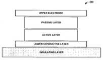
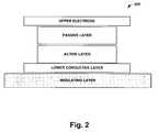
- a top and bottom electrodesandwich various film layers of functional or selective conductive, passive and active layers to form a memory cell.
- Such memory cellwhen subjected to an external stimulus, e.g. bias voltages, light radiation and the like, can be programmed (e.g. write/erase) via a desired impedance state induced in the memory cell.
- the desired impedance staterepresents one or more bits of information, and does not require a constant power supply or refresh cycles to maintain the desired information.
- the impedance state of the selectively conductive mediacan be read by applying a further external stimulus, such as an electric current.
- the read impedance staterepresents one or more bits of information.
- Switching between the various statescan be a function of the electrical field created in such memory cell. In general, such formed electrical field can in turn be a function of the thickness of layers sandwiched between the top and bottom electrodes, and the applied electrical voltage between the first and second electrodes.
- the memory cell functional zonemay contain an active layer based on organic and metalorganic conjugate polymers with active elements built into the main circuit and/or connected to the circuit or to the plane and/or built into the structure, with the elements forming or not forming a light emitting structure, or of an active layer based on organic, metalorganic and non-organic materials with instilled positive or negative ions, including molecular ions, and/or with instilled clusters based on solid electrolytes or with molecules and/or ions with an electric dipole element, and/or with clusters based on solid polymer and non-organic ferroelectrics, and/or with donor and acceptor molecules, and/or with organic and/or non-organic salts and/or acids and/or alkalis and/or water molecules which can dissociate in an electric field and/or under light radiation, and/or with non-organic and/or metalorganic and/or organic salts and/or molecules with variable valency of metals or atomic groups they contain.
- Such functional zonecan itself comprise of organic, metal organic, and non-organic materials, in the form of an active layer 108 and a passive layer 106 .
- the passive layer 106can in some instances act as a catalyst when forming the active layer 108 .
- a backbone of a conjugated organic moleculecan initially form adjacent the passive layer 106 , and grow or assemble away and substantially perpendicular to the passive layer surface.
- the backbones of the conjugated organic moleculecan be self aligned in a direction that traverses the two electrodes.
- the passive layercan be formed by a deposition process (e.g. thermal deposition, PVD, non-selective CVD, and the like) or by a complete sulfidation of pre-deposited thin Cu layer.
- such layercan include various organic, metal organic conjugate polymers.
- various light emitting materialsuch as; light emitting structure, photo resistance, or photo sensors can be part of the active layer 108 .
- additional material with donor/acceptor chargessuch as; molecules and/or ions with an electric dipole element, polymer ferroelectrics clusters, non-organic ferro-electrics, salts, alkalis and acids (organic or non organic), water molecules, materials with molecules that can dissociate in an electrical field and/or under radiation, organic salts and/or molecules with variable valency of metals, can also be employed as part of the active layer 108 .
- the active layer 108can also be comprised of a conjugated organic material, such as a small organic molecule and a conjugated polymer.
- a conjugated organic materialsuch as a small organic molecule and a conjugated polymer.
- a polymer backbone of the conjugated organic polymermay extend lengthwise between the electrodes 104 and 110 (e.g., generally substantially perpendicular to the inner, facing surfaces of the electrodes 104 and 110 ).
- the conjugated organic moleculecan be linear or branched such that the backbone retains its conjugated nature.
- Such conjugated moleculesare characterized in that they have overlapping ⁇ orbitals and that they can assume two or more resonant structures.
- the conjugated nature of the conjugated organic materialscontributes to the controllably conductive properties of the selectively conductive media.
- the memory cell 100can have a low impedance state, such as a very highly conductive state (very low impedance state), a highly conductive state (low impedance state), a conductive state (medium level impedance state), and a non-conductive state (high impedance state) thereby enabling the storage of multiple bits of information in a single organic memory cell, such as 2 or more bits of information or 4 or more bits of information (e.g., 4 states providing 2 bits of information, 8 states providing 3 bits of information, and the like.)
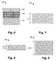
- FIG. 8a diagram depicting another organic layer 800 formed from a CVD process in accordance with an aspect of the present invention is illustrated.
- the organic layer 800is formed via a gas phase reaction process.
- the organic layer 800is formed in contact with a passive layer and an electrode.
- the organic polymer layer 800is comprised of polymer polyphenylacetylene (PPA).
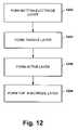
- a first or lower conductive conductoris deposited on an upper surface of an insulating layer.
- the first or lower conductormay be formed from materials selected from: aluminum, titanium, tungsten, platinum, palladium and their alloys and nitrides, conductive oxides, and amorphous carbon (a-C).
- the first or lower conductor layeris about 3000 ⁇ thick.
- the active layeris mixture of a polymer polythiophene with cyclopentadienyl groups, which may be deposited from solution by spin-coating.
- the active layeris about 500 ⁇ thick.
- the second conductor layeris amorphous carbon or palladium, which can be deposited on the upper surface of the active layer by magnetron co-sputtering.
- the second conductor layeris about 2000 ⁇ thick.
Landscapes
- Engineering & Computer Science (AREA)
- Chemical & Material Sciences (AREA)
- Computer Hardware Design (AREA)
- Nanotechnology (AREA)
- Crystallography & Structural Chemistry (AREA)
- Theoretical Computer Science (AREA)
- Mathematical Physics (AREA)
- Physics & Mathematics (AREA)
- Manufacturing & Machinery (AREA)
- Materials Engineering (AREA)
- Semiconductor Memories (AREA)
- Nitrogen And Oxygen Or Sulfur-Condensed Heterocyclic Ring Systems (AREA)
- Read Only Memory (AREA)
Abstract
Description
Claims (32)
Applications Claiming Priority (1)
| Application Number | Priority Date | Filing Date | Title |
|---|---|---|---|
| PCT/RU2001/000334WO2003017282A1 (en) | 2001-08-13 | 2001-08-13 | Memory cell |
Related Parent Applications (1)
| Application Number | Title | Priority Date | Filing Date |
|---|---|---|---|
| PCT/RU2001/000334Continuation-In-PartWO2003017282A1 (en) | 2001-08-13 | 2001-08-13 | Memory cell |
Publications (2)
| Publication Number | Publication Date |
|---|---|
| US20040159835A1 US20040159835A1 (en) | 2004-08-19 |
| US7026702B2true US7026702B2 (en) | 2006-04-11 |
Family
ID=20129643
Family Applications (5)
| Application Number | Title | Priority Date | Filing Date |
|---|---|---|---|
| US10/486,864Expired - LifetimeUS6992323B2 (en) | 2001-08-13 | 2001-08-13 | Memory cell |
| US10/238,880Expired - LifetimeUS6815286B2 (en) | 2001-08-13 | 2002-09-11 | Memory device |
| US10/414,353Expired - LifetimeUS6864522B2 (en) | 2001-08-13 | 2003-04-15 | Memory device |
| US10/776,850Expired - Fee RelatedUS7026702B2 (en) | 2001-08-13 | 2004-02-11 | Memory device |
| US10/776,870Expired - Fee RelatedUS7254053B2 (en) | 2001-08-13 | 2004-02-11 | Active programming and operation of a memory device |
Family Applications Before (3)
| Application Number | Title | Priority Date | Filing Date |
|---|---|---|---|
| US10/486,864Expired - LifetimeUS6992323B2 (en) | 2001-08-13 | 2001-08-13 | Memory cell |
| US10/238,880Expired - LifetimeUS6815286B2 (en) | 2001-08-13 | 2002-09-11 | Memory device |
| US10/414,353Expired - LifetimeUS6864522B2 (en) | 2001-08-13 | 2003-04-15 | Memory device |
Family Applications After (1)
| Application Number | Title | Priority Date | Filing Date |
|---|---|---|---|
| US10/776,870Expired - Fee RelatedUS7254053B2 (en) | 2001-08-13 | 2004-02-11 | Active programming and operation of a memory device |
Country Status (8)
| Country | Link |
|---|---|
| US (5) | US6992323B2 (en) |
| EP (1) | EP1434232B1 (en) |
| JP (1) | JP2005500682A (en) |
| KR (1) | KR100860134B1 (en) |
| CN (1) | CN100419906C (en) |
| BR (1) | BR0117103A (en) |
| DE (1) | DE60130586T2 (en) |
| WO (1) | WO2003017282A1 (en) |
Cited By (71)
| Publication number | Priority date | Publication date | Assignee | Title |
|---|---|---|---|---|
| US20060022347A1 (en)* | 2004-07-27 | 2006-02-02 | Campbell Kristy A | Amorphous carbon-based non-volatile memory |
| US20060035474A1 (en)* | 2004-08-10 | 2006-02-16 | Pavel Komilovich | Increasing retention time for memory devices |
| US20060214304A1 (en)* | 2005-03-25 | 2006-09-28 | Zhida Lan | Memory device with improved data retention |
| US20070034865A1 (en)* | 2005-08-12 | 2007-02-15 | Semiconductor Energy Laboratory Co., Ltd. | Memory device and a semiconductor device |
| US20070230235A1 (en)* | 2004-11-26 | 2007-10-04 | C/O Semiconductor Energy Laboratory Co., Ltd. | Semiconductor Device |
| US20080111124A1 (en)* | 2006-11-13 | 2008-05-15 | Samsung Electronics Co., Ltd. | Metallocenyl dendrimer, organic memory device using the same and fabrication method of the organic memory device |
| US20090014707A1 (en)* | 2006-10-20 | 2009-01-15 | Wei Lu | Non-volatile solid state resistive switching devices |
| US20110156012A1 (en)* | 2009-11-12 | 2011-06-30 | Sony Corporation | Double layer hardmask for organic devices |
| CN102130295A (en)* | 2010-12-17 | 2011-07-20 | 天津理工大学 | A resistive variable memory based on vanadium oxide thin film and its preparation method |
| US20120313070A1 (en)* | 2010-01-29 | 2012-12-13 | Williams R Stanley | Controlled switching memristor |
| US8374018B2 (en) | 2010-07-09 | 2013-02-12 | Crossbar, Inc. | Resistive memory using SiGe material |
| US8391049B2 (en) | 2010-09-29 | 2013-03-05 | Crossbar, Inc. | Resistor structure for a non-volatile memory device and method |
| US8394670B2 (en) | 2011-05-31 | 2013-03-12 | Crossbar, Inc. | Vertical diodes for non-volatile memory device |
| US8399881B2 (en) | 2005-03-25 | 2013-03-19 | Semiconductor Energy Laboratory Co., Ltd. | Memory element, memory device, and semiconductor device |
| US8404553B2 (en) | 2010-08-23 | 2013-03-26 | Crossbar, Inc. | Disturb-resistant non-volatile memory device and method |
| US8441835B2 (en) | 2010-06-11 | 2013-05-14 | Crossbar, Inc. | Interface control for improved switching in RRAM |
| US8450209B2 (en) | 2010-11-05 | 2013-05-28 | Crossbar, Inc. | p+ Polysilicon material on aluminum for non-volatile memory device and method |
| US8450710B2 (en) | 2011-05-27 | 2013-05-28 | Crossbar, Inc. | Low temperature p+ silicon junction material for a non-volatile memory device |
| US8467227B1 (en) | 2010-11-04 | 2013-06-18 | Crossbar, Inc. | Hetero resistive switching material layer in RRAM device and method |
| US8492195B2 (en) | 2010-08-23 | 2013-07-23 | Crossbar, Inc. | Method for forming stackable non-volatile resistive switching memory devices |
| US8519485B2 (en) | 2010-06-11 | 2013-08-27 | Crossbar, Inc. | Pillar structure for memory device and method |
| US8558212B2 (en) | 2010-09-29 | 2013-10-15 | Crossbar, Inc. | Conductive path in switching material in a resistive random access memory device and control |
| US8659929B2 (en) | 2011-06-30 | 2014-02-25 | Crossbar, Inc. | Amorphous silicon RRAM with non-linear device and operation |
| US8658476B1 (en) | 2012-04-20 | 2014-02-25 | Crossbar, Inc. | Low temperature P+ polycrystalline silicon material for non-volatile memory device |
| US8716098B1 (en) | 2012-03-09 | 2014-05-06 | Crossbar, Inc. | Selective removal method and structure of silver in resistive switching device for a non-volatile memory device |
| US8765566B2 (en) | 2012-05-10 | 2014-07-01 | Crossbar, Inc. | Line and space architecture for a non-volatile memory device |
| US8784690B2 (en) | 2010-08-20 | 2014-07-22 | Rhodia Operations | Polymer compositions, polymer films, polymer gels, polymer foams, and electronic devices containing such films, gels and foams |
| US8791010B1 (en) | 2010-12-31 | 2014-07-29 | Crossbar, Inc. | Silver interconnects for stacked non-volatile memory device and method |
| US8796658B1 (en) | 2012-05-07 | 2014-08-05 | Crossbar, Inc. | Filamentary based non-volatile resistive memory device and method |
| US8809831B2 (en) | 2010-07-13 | 2014-08-19 | Crossbar, Inc. | On/off ratio for non-volatile memory device and method |
| US8815696B1 (en) | 2010-12-31 | 2014-08-26 | Crossbar, Inc. | Disturb-resistant non-volatile memory device using via-fill and etchback technique |
| US8884261B2 (en) | 2010-08-23 | 2014-11-11 | Crossbar, Inc. | Device switching using layered device structure |
| US8889521B1 (en) | 2012-09-14 | 2014-11-18 | Crossbar, Inc. | Method for silver deposition for a non-volatile memory device |
| US8930174B2 (en) | 2010-12-28 | 2015-01-06 | Crossbar, Inc. | Modeling technique for resistive random access memory (RRAM) cells |
| US8934280B1 (en) | 2013-02-06 | 2015-01-13 | Crossbar, Inc. | Capacitive discharge programming for two-terminal memory cells |
| US8946673B1 (en) | 2012-08-24 | 2015-02-03 | Crossbar, Inc. | Resistive switching device structure with improved data retention for non-volatile memory device and method |
| US8946046B1 (en) | 2012-05-02 | 2015-02-03 | Crossbar, Inc. | Guided path for forming a conductive filament in RRAM |
| US8947908B2 (en) | 2010-11-04 | 2015-02-03 | Crossbar, Inc. | Hetero-switching layer in a RRAM device and method |
| US8946669B1 (en) | 2012-04-05 | 2015-02-03 | Crossbar, Inc. | Resistive memory device and fabrication methods |
| US8982647B2 (en) | 2012-11-14 | 2015-03-17 | Crossbar, Inc. | Resistive random access memory equalization and sensing |
| US9012307B2 (en) | 2010-07-13 | 2015-04-21 | Crossbar, Inc. | Two terminal resistive switching device structure and method of fabricating |
| US9087576B1 (en) | 2012-03-29 | 2015-07-21 | Crossbar, Inc. | Low temperature fabrication method for a three-dimensional memory device and structure |
| US9112145B1 (en) | 2013-01-31 | 2015-08-18 | Crossbar, Inc. | Rectified switching of two-terminal memory via real time filament formation |
| US9153623B1 (en) | 2010-12-31 | 2015-10-06 | Crossbar, Inc. | Thin film transistor steering element for a non-volatile memory device |
| US9191000B2 (en) | 2011-07-29 | 2015-11-17 | Crossbar, Inc. | Field programmable gate array utilizing two-terminal non-volatile memory |
| US9252191B2 (en) | 2011-07-22 | 2016-02-02 | Crossbar, Inc. | Seed layer for a p+ silicon germanium material for a non-volatile memory device and method |
| US9312483B2 (en) | 2012-09-24 | 2016-04-12 | Crossbar, Inc. | Electrode structure for a non-volatile memory device and method |
| US9324942B1 (en) | 2013-01-31 | 2016-04-26 | Crossbar, Inc. | Resistive memory cell with solid state diode |
| US9401475B1 (en) | 2010-08-23 | 2016-07-26 | Crossbar, Inc. | Method for silver deposition for a non-volatile memory device |
| US9406379B2 (en) | 2013-01-03 | 2016-08-02 | Crossbar, Inc. | Resistive random access memory with non-linear current-voltage relationship |
| US9412790B1 (en) | 2012-12-04 | 2016-08-09 | Crossbar, Inc. | Scalable RRAM device architecture for a non-volatile memory device and method |
| US9520557B2 (en) | 2008-10-20 | 2016-12-13 | The Regents Of The University Of Michigan | Silicon based nanoscale crossbar memory |
| US9543359B2 (en) | 2011-05-31 | 2017-01-10 | Crossbar, Inc. | Switching device having a non-linear element |
| US9564587B1 (en) | 2011-06-30 | 2017-02-07 | Crossbar, Inc. | Three-dimensional two-terminal memory with enhanced electric field and segmented interconnects |
| US9570678B1 (en) | 2010-06-08 | 2017-02-14 | Crossbar, Inc. | Resistive RAM with preferental filament formation region and methods |
| US9576616B2 (en) | 2012-10-10 | 2017-02-21 | Crossbar, Inc. | Non-volatile memory with overwrite capability and low write amplification |
| US9583701B1 (en) | 2012-08-14 | 2017-02-28 | Crossbar, Inc. | Methods for fabricating resistive memory device switching material using ion implantation |
| USRE46335E1 (en) | 2010-11-04 | 2017-03-07 | Crossbar, Inc. | Switching device having a non-linear element |
| US9601692B1 (en) | 2010-07-13 | 2017-03-21 | Crossbar, Inc. | Hetero-switching layer in a RRAM device and method |
| US9601690B1 (en) | 2011-06-30 | 2017-03-21 | Crossbar, Inc. | Sub-oxide interface layer for two-terminal memory |
| US9620206B2 (en) | 2011-05-31 | 2017-04-11 | Crossbar, Inc. | Memory array architecture with two-terminal memory cells |
| US9627443B2 (en) | 2011-06-30 | 2017-04-18 | Crossbar, Inc. | Three-dimensional oblique two-terminal memory with enhanced electric field |
| US9633723B2 (en) | 2011-06-23 | 2017-04-25 | Crossbar, Inc. | High operating speed resistive random access memory |
| US9685608B2 (en) | 2012-04-13 | 2017-06-20 | Crossbar, Inc. | Reduced diffusion in metal electrode for two-terminal memory |
| US9729155B2 (en) | 2011-07-29 | 2017-08-08 | Crossbar, Inc. | Field programmable gate array utilizing two-terminal non-volatile memory |
| US9735358B2 (en) | 2012-08-14 | 2017-08-15 | Crossbar, Inc. | Noble metal / non-noble metal electrode for RRAM applications |
| US9741765B1 (en) | 2012-08-14 | 2017-08-22 | Crossbar, Inc. | Monolithically integrated resistive memory using integrated-circuit foundry compatible processes |
| WO2018102876A1 (en) | 2016-12-07 | 2018-06-14 | Australian Advanced Materials Pty Ltd | Resistive switching memory |
| US10056907B1 (en) | 2011-07-29 | 2018-08-21 | Crossbar, Inc. | Field programmable gate array utilizing two-terminal non-volatile memory |
| US10290801B2 (en) | 2014-02-07 | 2019-05-14 | Crossbar, Inc. | Scalable silicon based resistive memory device |
| US11068620B2 (en) | 2012-11-09 | 2021-07-20 | Crossbar, Inc. | Secure circuit integrated with memory layer |
Families Citing this family (196)
| Publication number | Priority date | Publication date | Assignee | Title |
|---|---|---|---|---|
| WO2002091496A2 (en) | 2001-05-07 | 2002-11-14 | Advanced Micro Devices, Inc. | Reversible field-programmable electric interconnects |
| KR100900080B1 (en) | 2001-05-07 | 2009-06-01 | 어드밴스드 마이크로 디바이시즈, 인코포레이티드 | Memory device having self-assembled polymer film and manufacturing method thereof |
| US6873540B2 (en) | 2001-05-07 | 2005-03-29 | Advanced Micro Devices, Inc. | Molecular memory cell |
| WO2002091495A2 (en) | 2001-05-07 | 2002-11-14 | Coatue Corporation | Molecular memory device |
| CN100367528C (en) | 2001-05-07 | 2008-02-06 | 先进微装置公司 | Switching device with memory effect |
| US6768157B2 (en) | 2001-08-13 | 2004-07-27 | Advanced Micro Devices, Inc. | Memory device |
| US6806526B2 (en) | 2001-08-13 | 2004-10-19 | Advanced Micro Devices, Inc. | Memory device |
| US6838720B2 (en) | 2001-08-13 | 2005-01-04 | Advanced Micro Devices, Inc. | Memory device with active passive layers |
| WO2003017282A1 (en) | 2001-08-13 | 2003-02-27 | Advanced Micro Devices, Inc. | Memory cell |
| US6858481B2 (en) | 2001-08-13 | 2005-02-22 | Advanced Micro Devices, Inc. | Memory device with active and passive layers |
| US9269043B2 (en) | 2002-03-12 | 2016-02-23 | Knowm Tech, Llc | Memristive neural processor utilizing anti-hebbian and hebbian technology |
| US7392230B2 (en) | 2002-03-12 | 2008-06-24 | Knowmtech, Llc | Physical neural network liquid state machine utilizing nanotechnology |
| US8156057B2 (en) | 2003-03-27 | 2012-04-10 | Knowm Tech, Llc | Adaptive neural network utilizing nanotechnology-based components |
| US6889216B2 (en) | 2002-03-12 | 2005-05-03 | Knowm Tech, Llc | Physical neural network design incorporating nanotechnology |
| US7398259B2 (en) | 2002-03-12 | 2008-07-08 | Knowmtech, Llc | Training of a physical neural network |
| US7412428B2 (en) | 2002-03-12 | 2008-08-12 | Knowmtech, Llc. | Application of hebbian and anti-hebbian learning to nanotechnology-based physical neural networks |
| US7752151B2 (en) | 2002-06-05 | 2010-07-06 | Knowmtech, Llc | Multilayer training in a physical neural network formed utilizing nanotechnology |
| US7827131B2 (en) | 2002-08-22 | 2010-11-02 | Knowm Tech, Llc | High density synapse chip using nanoparticles |
| US7012276B2 (en) | 2002-09-17 | 2006-03-14 | Advanced Micro Devices, Inc. | Organic thin film Zener diodes |
| US6836398B1 (en)* | 2002-10-31 | 2004-12-28 | Advanced Micro Devices, Inc. | System and method of forming a passive layer by a CMP process |
| WO2004070789A2 (en)* | 2003-02-03 | 2004-08-19 | The Regent Of The University Of California | Rewritable nano-surface organic electrical bistable devices |
| US6656763B1 (en)* | 2003-03-10 | 2003-12-02 | Advanced Micro Devices, Inc. | Spin on polymers for organic memory devices |
| US6995445B2 (en)* | 2003-03-14 | 2006-02-07 | The Trustees Of Princeton University | Thin film organic position sensitive detectors |
| US7297621B2 (en)* | 2003-04-15 | 2007-11-20 | California Institute Of Technology | Flexible carbon-based ohmic contacts for organic transistors |
| US6977389B2 (en)* | 2003-06-02 | 2005-12-20 | Advanced Micro Devices, Inc. | Planar polymer memory device |
| US6921912B2 (en)* | 2003-06-03 | 2005-07-26 | Micron Technology, Inc. | Diode/superionic conductor/polymer memory structure |
| US20050006640A1 (en)* | 2003-06-26 | 2005-01-13 | Jackson Warren B. | Polymer-based memory element |
| US6787458B1 (en)* | 2003-07-07 | 2004-09-07 | Advanced Micro Devices, Inc. | Polymer memory device formed in via opening |
| US7259039B2 (en)* | 2003-07-09 | 2007-08-21 | Spansion Llc | Memory device and methods of using and making the device |
| JP4321524B2 (en)* | 2003-07-18 | 2009-08-26 | 日本電気株式会社 | Switching element, switching element driving method, rewritable logic integrated circuit, and memory element |
| US7426501B2 (en) | 2003-07-18 | 2008-09-16 | Knowntech, Llc | Nanotechnology neural network methods and systems |
| KR100615586B1 (en)* | 2003-07-23 | 2006-08-25 | 삼성전자주식회사 | Phase change memory device having a local phase change region in a porous dielectric film and a method of manufacturing the same |
| US7274035B2 (en)* | 2003-09-03 | 2007-09-25 | The Regents Of The University Of California | Memory devices based on electric field programmable films |
| DE10342026A1 (en)* | 2003-09-11 | 2005-04-28 | Infineon Technologies Ag | Memory cell with ion conduction storage mechanism and method for its production |
| US6852586B1 (en)* | 2003-10-01 | 2005-02-08 | Advanced Micro Devices, Inc. | Self assembly of conducting polymer for formation of polymer memory cell |
| US7015504B2 (en)* | 2003-11-03 | 2006-03-21 | Advanced Micro Devices, Inc. | Sidewall formation for high density polymer memory element array |
| JP2005150156A (en)* | 2003-11-11 | 2005-06-09 | Toshiba Corp | Magnetic storage |
| WO2005086627A2 (en)* | 2003-12-03 | 2005-09-22 | The Regents Of The University Of California | Three-terminal electrical bistable devices |
| JP4385778B2 (en)* | 2004-01-29 | 2009-12-16 | ソニー株式会社 | Storage device |
| US6956761B2 (en)* | 2004-03-10 | 2005-10-18 | Micron Technology, Inc. | Method to manufacture polymer memory with copper ion switching species |
| CA2500938A1 (en)* | 2004-03-24 | 2005-09-24 | Rohm And Haas Company | Memory devices based on electric field programmable films |
| ATE486369T1 (en)* | 2004-03-26 | 2010-11-15 | Nxp Bv | ELECTRICAL DEVICE COMPRISING A PHASE CHANGE MATERIAL |
| US7205595B2 (en)* | 2004-03-31 | 2007-04-17 | Intel Corporation | Polymer memory device with electron traps |
| US7608855B2 (en)* | 2004-04-02 | 2009-10-27 | Spansion Llc | Polymer dielectrics for memory element array interconnect |
| WO2006001923A2 (en)* | 2004-05-17 | 2006-01-05 | The Regents Of The University Of California | Bistable nanoparticle- polymer composite for use in memory devices |
| US20050274609A1 (en)* | 2004-05-18 | 2005-12-15 | Yong Chen | Composition of matter which results in electronic switching through intra- or inter- molecular charge transfer, or charge transfer between molecules and electrodes induced by an electrical field |
| DE102004024610B3 (en)* | 2004-05-18 | 2005-12-29 | Infineon Technologies Ag | Solid electrolyte switching element |
| US7554111B2 (en)* | 2004-05-20 | 2009-06-30 | The Regents Of The University Of California | Nanoparticle-polymer bistable devices |
| DE102004031135A1 (en)* | 2004-06-28 | 2006-01-19 | Infineon Technologies Ag | Resistive semiconductor element based on a solid-state ion conductor |
| US7157732B2 (en)* | 2004-07-01 | 2007-01-02 | Spansion Llc | Switchable memory diode-a new memory device |
| US7199394B2 (en)* | 2004-08-17 | 2007-04-03 | Spansion Llc | Polymer memory device with variable period of retention time |
| US7289353B2 (en) | 2004-08-17 | 2007-10-30 | Spansion, Llc | Systems and methods for adjusting programming thresholds of polymer memory cells |
| US7166543B2 (en)* | 2004-08-30 | 2007-01-23 | Micron Technology, Inc. | Methods for forming an enriched metal oxide surface for use in a semiconductor device |
| DE102004046392A1 (en)* | 2004-09-24 | 2006-04-06 | Infineon Technologies Ag | Semiconductor memory |
| WO2006039439A2 (en) | 2004-09-30 | 2006-04-13 | Cummins-Allison Corp. | Magnetic detection system for use in currency processing and method and apparatus for using the same |
| US7557782B2 (en)* | 2004-10-20 | 2009-07-07 | Hewlett-Packard Development Company, L.P. | Display device including variable optical element and programmable resistance element |
| GB2437188A (en)* | 2004-10-28 | 2007-10-17 | Univ California | Organic-complex thin film for nonvolatile memory applications |
| US7221599B1 (en)* | 2004-11-01 | 2007-05-22 | Spansion, Llc | Polymer memory cell operation |
| US7876596B2 (en)* | 2004-11-08 | 2011-01-25 | Waseda University | Memory element and method for manufacturing same |
| KR100657911B1 (en)* | 2004-11-10 | 2006-12-14 | 삼성전자주식회사 | Nonvolatile Memory Device with One Resistor and One Diode |
| KR100651656B1 (en)* | 2004-11-29 | 2006-12-01 | 한국과학기술연구원 | Phase Change Memory Cells with Transparent Conductive Oxide Electrode Contact Materials |
| EP1820215A4 (en)* | 2004-12-07 | 2008-11-12 | Semiconductor Energy Lab | MEMORY DEVICE AND SEMICONDUCTOR DEVICE |
| FR2880177B1 (en) | 2004-12-23 | 2007-05-18 | Commissariat Energie Atomique | MEMORY PMC HAVING IMPROVED RETENTION TIME AND WRITING SPEED |
| US7102156B1 (en)* | 2004-12-23 | 2006-09-05 | Spansion Llc Advanced Micro Devices, Inc | Memory elements using organic active layer |
| US7208757B1 (en)* | 2004-12-23 | 2007-04-24 | Spansion Llc | Memory element with nitrogen-containing active layer |
| US7273766B1 (en)* | 2005-01-12 | 2007-09-25 | Spansion Llc | Variable density and variable persistent organic memory devices, methods, and fabrication |
| US7084062B1 (en) | 2005-01-12 | 2006-08-01 | Advanced Micro Devices, Inc. | Use of Ta-capped metal line to improve formation of memory element films |
| KR101067582B1 (en)* | 2005-01-20 | 2011-09-27 | 삼성전자주식회사 | Multi-State Driving Method of Memory Devices |
| DE102005004107A1 (en)* | 2005-01-28 | 2006-08-17 | Infineon Technologies Ag | Integrated semiconductor memory with an arrangement of nonvolatile memory cells and method |
| US7502769B2 (en) | 2005-01-31 | 2009-03-10 | Knowmtech, Llc | Fractal memory and computational methods and systems based on nanotechnology |
| KR101078125B1 (en)* | 2005-02-07 | 2011-10-28 | 삼성전자주식회사 | Nonvolatile Nano-channel Memory Device using Mesoporous Material |
| KR101036975B1 (en)* | 2005-02-14 | 2011-05-25 | 삼성전자주식회사 | Resistive memory devices with resistor part for controlling switching window |
| US8193606B2 (en) | 2005-02-28 | 2012-06-05 | Semiconductor Energy Laboratory Co., Ltd. | Semiconductor device including a memory element |
| KR100682939B1 (en) | 2005-03-16 | 2007-02-15 | 삼성전자주식회사 | Semiconductor memory device using solid electrolyte of three-dimensional structure and manufacturing method thereof |
| US7145824B2 (en)* | 2005-03-22 | 2006-12-05 | Spansion Llc | Temperature compensation of thin film diode voltage threshold in memory sensing circuit |
| US7579631B2 (en)* | 2005-03-22 | 2009-08-25 | Spansion Llc | Variable breakdown characteristic diode |
| US7180770B2 (en)* | 2005-03-24 | 2007-02-20 | Hewlett-Packard Development Company, L.P. | Series diode thermally assisted MRAM |
| US7307321B1 (en)* | 2005-03-25 | 2007-12-11 | Spansion Llc | Memory device with improved data retention |
| US8098521B2 (en)* | 2005-03-31 | 2012-01-17 | Spansion Llc | Method of providing an erase activation energy of a memory device |
| US7344913B1 (en) | 2005-04-06 | 2008-03-18 | Spansion Llc | Spin on memory cell active layer doped with metal ions |
| US7776682B1 (en)* | 2005-04-20 | 2010-08-17 | Spansion Llc | Ordered porosity to direct memory element formation |
| CN101167189B (en)* | 2005-04-27 | 2013-09-18 | 株式会社半导体能源研究所 | Manufacturing method of semiconductor device |
| US20060245235A1 (en)* | 2005-05-02 | 2006-11-02 | Advanced Micro Devices, Inc. | Design and operation of a resistance switching memory cell with diode |
| US7812404B2 (en)* | 2005-05-09 | 2010-10-12 | Sandisk 3D Llc | Nonvolatile memory cell comprising a diode and a resistance-switching material |
| US20060256608A1 (en)* | 2005-05-11 | 2006-11-16 | Spansion Llc | Resistive memory device with improved data retention and reduced power |
| JP4552752B2 (en)* | 2005-05-16 | 2010-09-29 | ソニー株式会社 | Storage element manufacturing method and storage device manufacturing method |
| NO324539B1 (en)* | 2005-06-14 | 2007-11-19 | Thin Film Electronics Asa | Process in the manufacture of a ferroelectric memory device |
| US7286388B1 (en)* | 2005-06-23 | 2007-10-23 | Spansion Llc | Resistive memory device with improved data retention |
| US7361586B2 (en)* | 2005-07-01 | 2008-04-22 | Spansion Llc | Preamorphization to minimize void formation |
| US20070009821A1 (en)* | 2005-07-08 | 2007-01-11 | Charlotte Cutler | Devices containing multi-bit data |
| US7746533B2 (en)* | 2005-07-11 | 2010-06-29 | The University Of Connecticut | Electrochromic devices utilizing very low band gap conjugated counter electrodes: preparation and use |
| RU2297625C1 (en)* | 2005-09-14 | 2007-04-20 | Сергей Анатольевич Ермаков | Electrolytic memory cell for electronic memorizing devices and method for manufacturing said devices |
| US7582893B2 (en)* | 2005-09-15 | 2009-09-01 | Spansion Llc | Semiconductor memory device comprising one or more injecting bilayer electrodes |
| US7633129B1 (en)* | 2005-09-16 | 2009-12-15 | Spansion Llc | Memory devices with active and passive layers having multiple self-assembled sublayers |
| US7307280B1 (en)* | 2005-09-16 | 2007-12-11 | Spansion Llc | Memory devices with active and passive doped sol-gel layers |
| US7268364B2 (en)* | 2005-09-23 | 2007-09-11 | Aculon, Inc. | Hybrid devices |
| US7632706B2 (en)* | 2005-10-21 | 2009-12-15 | Spansion Llc | System and method for processing an organic memory cell |
| US7741638B2 (en)* | 2005-11-23 | 2010-06-22 | Hewlett-Packard Development Company, L.P. | Control layer for a nanoscale electronic switching device |
| US8173995B2 (en)* | 2005-12-23 | 2012-05-08 | E. I. Du Pont De Nemours And Company | Electronic device including an organic active layer and process for forming the electronic device |
| FR2895531B1 (en)* | 2005-12-23 | 2008-05-09 | Commissariat Energie Atomique | IMPROVED METHOD FOR MAKING MEMORY CELLS OF THE PMC TYPE |
| KR20070075812A (en)* | 2006-01-16 | 2007-07-24 | 삼성전자주식회사 | Resistive memory device including an amorphous solid electrolyte layer in a storage node |
| KR101206605B1 (en)* | 2006-02-02 | 2012-11-29 | 삼성전자주식회사 | Organic memory devices and preparation method thereof |
| JP5417709B2 (en)* | 2006-02-09 | 2014-02-19 | 日本電気株式会社 | Switching element, rewritable logic integrated circuit, and memory element |
| US8089110B1 (en)* | 2006-02-09 | 2012-01-03 | Spansion Llc | Switchable memory diodes based on ferroelectric/conjugated polymer heterostructures and/or their composites |
| US7605410B2 (en)* | 2006-02-23 | 2009-10-20 | Semiconductor Energy Laboratory Co., Ltd. | Semiconductor device and manufacturing method thereof |
| CN101401209B (en)* | 2006-03-10 | 2011-05-25 | 株式会社半导体能源研究所 | Memory element and semiconductor device |
| US7875871B2 (en)* | 2006-03-31 | 2011-01-25 | Sandisk 3D Llc | Heterojunction device comprising a semiconductor and a resistivity-switching oxide or nitride |
| US8502198B2 (en)* | 2006-04-28 | 2013-08-06 | Hewlett-Packard Development Company, L.P. | Switching device and methods for controlling electron tunneling therein |
| US7719001B2 (en)* | 2006-06-28 | 2010-05-18 | Semiconductor Energy Laboratory Co., Ltd | Semiconductor device with metal oxides and an organic compound |
| US8115282B2 (en)* | 2006-07-25 | 2012-02-14 | Adesto Technology Corporation | Memory cell device and method of manufacture |
| EP1883109B1 (en)* | 2006-07-28 | 2013-05-15 | Semiconductor Energy Laboratory Co., Ltd. | Memory element and method of manufacturing thereof |
| FR2905028B1 (en)* | 2006-08-21 | 2008-12-19 | Commissariat Energie Atomique | ELECTROCHEMICAL MEMORY DEVICE |
| KR100836759B1 (en)* | 2006-10-04 | 2008-06-10 | 삼성전자주식회사 | Organic memory device and method of forming the same |
| US8790819B1 (en)* | 2006-10-06 | 2014-07-29 | Greatbatch Ltd. | Implantable medical assembly |
| US7988057B2 (en) | 2006-11-28 | 2011-08-02 | Semiconductor Energy Laboratory Co., Ltd. | Memory device and semiconductor device |
| US7902086B2 (en)* | 2006-12-08 | 2011-03-08 | Spansion Llc | Prevention of oxidation of carrier ions to improve memory retention properties of polymer memory cell |
| US7449742B2 (en)* | 2006-12-20 | 2008-11-11 | Spansion Llc | Memory device with active layer of dendrimeric material |
| US7930257B2 (en) | 2007-01-05 | 2011-04-19 | Knowm Tech, Llc | Hierarchical temporal memory utilizing nanotechnology |
| KR101313784B1 (en)* | 2007-01-12 | 2013-10-01 | 삼성전자주식회사 | Resistive random access memory device and method for manufacturing the same |
| US7667220B2 (en)* | 2007-01-19 | 2010-02-23 | Macronix International Co., Ltd. | Multilevel-cell memory structures employing multi-memory with tungsten oxides and manufacturing method |
| US8373148B2 (en)* | 2007-04-26 | 2013-02-12 | Spansion Llc | Memory device with improved performance |
| US8233308B2 (en)* | 2007-06-29 | 2012-07-31 | Sandisk 3D Llc | Memory cell that employs a selectively deposited reversible resistance-switching element and methods of forming the same |
| US7824956B2 (en) | 2007-06-29 | 2010-11-02 | Sandisk 3D Llc | Memory cell that employs a selectively grown reversible resistance-switching element and methods of forming the same |
| US7902537B2 (en) | 2007-06-29 | 2011-03-08 | Sandisk 3D Llc | Memory cell that employs a selectively grown reversible resistance-switching element and methods of forming the same |
| US20090104756A1 (en)* | 2007-06-29 | 2009-04-23 | Tanmay Kumar | Method to form a rewriteable memory cell comprising a diode and a resistivity-switching grown oxide |
| JP5227544B2 (en)* | 2007-07-12 | 2013-07-03 | 株式会社日立製作所 | Semiconductor device |
| RU2376677C2 (en)* | 2007-07-23 | 2009-12-20 | Физико-технологический институт Российской академии наук (статус государственного учреждения) | Memory cell with conducting layer-dielectric-conducting layer structure |
| US8946020B2 (en)* | 2007-09-06 | 2015-02-03 | Spansion, Llc | Method of forming controllably conductive oxide |
| FR2922368A1 (en)* | 2007-10-16 | 2009-04-17 | Commissariat Energie Atomique | METHOD FOR MANUFACTURING A CBRAM MEMORY HAVING IMPROVED RELIABILITY |
| US7558101B1 (en)* | 2007-12-14 | 2009-07-07 | Spansion Llc | Scan sensing method that improves sensing margins |
| FR2928768B1 (en) | 2008-03-13 | 2010-04-09 | Commissariat Energie Atomique | NON-VOLATILE ELECTROCHEMICAL MEMORY DEVICE |
| US8133793B2 (en) | 2008-05-16 | 2012-03-13 | Sandisk 3D Llc | Carbon nano-film reversible resistance-switchable elements and methods of forming the same |
| KR101435517B1 (en)* | 2008-05-28 | 2014-08-29 | 삼성전자주식회사 | Image sensor using photodetecting molecule and driving method thereof |
| US8569730B2 (en)* | 2008-07-08 | 2013-10-29 | Sandisk 3D Llc | Carbon-based interface layer for a memory device and methods of forming the same |
| US20100032640A1 (en)* | 2008-08-07 | 2010-02-11 | Sandisk 3D Llc | Memory cell that includes a carbon-based memory element and methods of forming the same |
| US20100108976A1 (en)* | 2008-10-30 | 2010-05-06 | Sandisk 3D Llc | Electronic devices including carbon-based films, and methods of forming such devices |
| US8835892B2 (en)* | 2008-10-30 | 2014-09-16 | Sandisk 3D Llc | Electronic devices including carbon nano-tube films having boron nitride-based liners, and methods of forming the same |
| US8421050B2 (en)* | 2008-10-30 | 2013-04-16 | Sandisk 3D Llc | Electronic devices including carbon nano-tube films having carbon-based liners, and methods of forming the same |
| US8183121B2 (en) | 2009-03-31 | 2012-05-22 | Sandisk 3D Llc | Carbon-based films, and methods of forming the same, having dielectric filler material and exhibiting reduced thermal resistance |
| US8519372B2 (en) | 2009-07-30 | 2013-08-27 | Hewlett-Packard Development Company, L.P. | Electroforming-free nanoscale switching device |
| WO2011041772A2 (en)* | 2009-10-02 | 2011-04-07 | The University Of Memphis Research Foundation | Memory devices, methods of storing and reading data, smm junctions, and methods of preparing alumina substrates |
| US8551855B2 (en)* | 2009-10-23 | 2013-10-08 | Sandisk 3D Llc | Memory cell that includes a carbon-based reversible resistance switching element compatible with a steering element, and methods of forming the same |
| US8481396B2 (en)* | 2009-10-23 | 2013-07-09 | Sandisk 3D Llc | Memory cell that includes a carbon-based reversible resistance switching element compatible with a steering element, and methods of forming the same |
| US8279665B2 (en)* | 2009-11-23 | 2012-10-02 | International Business Machines Corporation | Memory cell and select element |
| US8551850B2 (en)* | 2009-12-07 | 2013-10-08 | Sandisk 3D Llc | Methods of forming a reversible resistance-switching metal-insulator-metal structure |
| US8389375B2 (en)* | 2010-02-11 | 2013-03-05 | Sandisk 3D Llc | Memory cell formed using a recess and methods for forming the same |
| US8416609B2 (en) | 2010-02-15 | 2013-04-09 | Micron Technology, Inc. | Cross-point memory cells, non-volatile memory arrays, methods of reading a memory cell, methods of programming a memory cell, methods of writing to and reading from a memory cell, and computer systems |
| US8437174B2 (en) | 2010-02-15 | 2013-05-07 | Micron Technology, Inc. | Memcapacitor devices, field effect transistor devices, non-volatile memory arrays, and methods of programming |
| US8237146B2 (en)* | 2010-02-24 | 2012-08-07 | Sandisk 3D Llc | Memory cell with silicon-containing carbon switching layer and methods for forming the same |
| CN101807669A (en)* | 2010-03-29 | 2010-08-18 | 南京大学 | Organic memory |
| US8471360B2 (en) | 2010-04-14 | 2013-06-25 | Sandisk 3D Llc | Memory cell with carbon switching material having a reduced cross-sectional area and methods for forming the same |
| US8735858B2 (en) | 2010-04-30 | 2014-05-27 | Hewlett-Packard Development Company, L.P. | Ionic devices with interacting species |
| KR20130119322A (en)* | 2010-05-11 | 2013-10-31 | 예다 리서치 앤드 디벨럽먼트 캄파니 리미티드 | Solid, multi-state molecular random access memory(ram) |
| US8634224B2 (en) | 2010-08-12 | 2014-01-21 | Micron Technology, Inc. | Memory cells, non-volatile memory arrays, methods of operating memory cells, methods of writing to and reading from a memory cell, and methods of programming a memory cell |
| GB2488583A (en)* | 2011-03-03 | 2012-09-05 | Nds Ltd | Preventing unauthorized access to data stored in non-volatile memories |
| US8361651B2 (en) | 2011-04-29 | 2013-01-29 | Toyota Motor Engineering & Manufacturing North America, Inc. | Active material for rechargeable battery |
| KR20130022819A (en)* | 2011-08-26 | 2013-03-07 | 한양대학교 산학협력단 | Non-volatile polymer memory devices containing buffer layer and fabrication method thereof |
| CN103208514B (en)* | 2012-01-14 | 2017-05-17 | 盛况 | Semiconductor device containing metals and preparation method of semiconductor device |
| US9653159B2 (en)* | 2012-01-18 | 2017-05-16 | Xerox Corporation | Memory device based on conductance switching in polymer/electrolyte junctions |
| US8673493B2 (en) | 2012-05-29 | 2014-03-18 | Toyota Motor Engineering & Manufacturing North America, Inc. | Indium-tin binary anodes for rechargeable magnesium-ion batteries |
| US8647770B2 (en) | 2012-05-30 | 2014-02-11 | Toyota Motor Engineering & Manufacturing North America, Inc. | Bismuth-tin binary anodes for rechargeable magnesium-ion batteries |
| US9685619B2 (en) | 2012-07-09 | 2017-06-20 | Yeda Research And Development Co. Ltd. | Logic circuits with plug and play solid-state molecular chips |
| CN103078055B (en)* | 2013-01-04 | 2015-06-03 | 华中科技大学 | Unit, device and method for simulating biological neuronal synapsis |
| US9130157B2 (en) | 2013-07-26 | 2015-09-08 | Micron Technology, Inc. | Memory cells having a number of conductive diffusion barrier materials and manufacturing methods |
| CN104518083B (en)* | 2013-09-26 | 2017-03-15 | 中国科学院宁波材料技术与工程研究所 | A kind of memory element of resistive random access memory (RRAM) and preparation method thereof |
| IL229525A0 (en) | 2013-11-20 | 2014-01-30 | Yeda Res & Dev | Metal-based tris-bipyridyl complexes and uses thereof in electrochromic applications |
| US20170047513A1 (en)* | 2014-04-21 | 2017-02-16 | University Of Washington | Proton resistive memory devices and methods |
| DE102015000120A1 (en)* | 2015-01-07 | 2016-07-07 | Merck Patent Gmbh | Electronic component |
| WO2016152492A1 (en)* | 2015-03-26 | 2016-09-29 | 富士フイルム株式会社 | Matrix device and method for producing matrix device |
| CN104894530B (en)* | 2015-06-09 | 2018-02-02 | 国家纳米科学中心 | A kind of two-dimentional transition metal chalcogenide film and its preparation method and application |
| US10483462B1 (en)* | 2015-06-17 | 2019-11-19 | Crossbar, Inc. | Formation of structurally robust nanoscale Ag-based conductive structure |
| WO2017052546A1 (en)* | 2015-09-24 | 2017-03-30 | Hewlett Packard Enterprise Development Lp | Selector with porous oxide layer |
| DE102016003461A1 (en)* | 2016-03-23 | 2017-09-28 | Forschungszentrum Jülich GmbH | Method for producing a memory, memory, and use of the memory |
| CN105932154B (en)* | 2016-05-17 | 2018-10-09 | 浙江师范大学 | Material with stable threshold resistance transformation characteristic and dynamic RAM part |
| US10204997B2 (en)* | 2016-09-21 | 2019-02-12 | Boe Technology Group Co., Ltd. | Thin film transistor, display substrate and display panel having the same, and fabricating method thereof |
| US10352971B2 (en)* | 2016-09-30 | 2019-07-16 | Arm Ltd. | Voltage detection with correlated electron switch |
| US9947379B1 (en) | 2016-10-06 | 2018-04-17 | National Technology & Engineering Solutions Of Sandia, Llc | Device and methods for writing and erasing analog information in small memory units via voltage pulses |
| US10164179B2 (en)* | 2017-01-13 | 2018-12-25 | International Business Machines Corporation | Memristive device based on alkali-doping of transitional metal oxides |
| US10429343B1 (en) | 2017-02-09 | 2019-10-01 | National Technology & Engineering Solutions Of Sandia, Llc | Tunable ionic electronic transistor |
| US10229736B2 (en)* | 2017-06-22 | 2019-03-12 | International Business Machines Corporation | Memristive device based on reversible intercalated ion transfer between two meta-stable phases |
| CN109957194A (en)* | 2017-12-14 | 2019-07-02 | 中国科学院深圳先进技术研究院 | A kind of composite film and its production method |
| US10586591B2 (en) | 2018-01-08 | 2020-03-10 | International Business Machines Corporation | High speed thin film two terminal resistive memory |
| US10777267B2 (en) | 2018-01-08 | 2020-09-15 | International Business Machines Corporation | High speed thin film two terminal resistive memory |
| US10700093B1 (en) | 2018-12-20 | 2020-06-30 | Sandisk Technologies Llc | Ferroelectric memory devices employing conductivity modulation of a thin semiconductor material or a two-dimensional charge carrier gas and methods of operating the same |
| US11177284B2 (en) | 2018-12-20 | 2021-11-16 | Sandisk Technologies Llc | Ferroelectric memory devices containing a two-dimensional charge carrier gas channel and methods of making the same |
| US11455521B2 (en) | 2019-03-01 | 2022-09-27 | International Business Machines Corporation | Neuromorphic device driven by copper ion intercalation |
| CN110224064B (en)* | 2019-06-26 | 2020-10-27 | 西安交通大学 | BN (Al) film-based resistance switch and preparation method thereof |
| WO2021038475A1 (en)* | 2019-08-27 | 2021-03-04 | Oti Lumionics Inc. | Light transmissive electrode for light emitting devices |
| US11222920B2 (en) | 2020-02-04 | 2022-01-11 | Western Digital Technologies, Inc. | Magnetic device including multiferroic regions and methods of forming the same |
| US11107516B1 (en) | 2020-02-24 | 2021-08-31 | Sandisk Technologies Llc | Ferroelectric memory devices containing a two-dimensional charge carrier gas channel and methods of making the same |
| US11264562B1 (en) | 2020-08-27 | 2022-03-01 | Western Digital Technologies, Inc. | Multiferroic-assisted voltage controlled magnetic anisotropy memory device and methods of manufacturing the same |
| US11276446B1 (en) | 2020-08-27 | 2022-03-15 | Western Digital Technologies, Inc. | Multiferroic-assisted voltage controlled magnetic anisotropy memory device and methods of manufacturing the same |
| TWI775427B (en) | 2021-05-07 | 2022-08-21 | 財團法人工業技術研究院 | Ferroelectric memories |
| US12366881B1 (en) | 2021-08-23 | 2025-07-22 | National Technology & Engineering Solutions Of Sandia, Llc | Programming analog memory elements in a neomorphic computing system |
| JP2023081627A (en)* | 2021-12-01 | 2023-06-13 | キオクシア株式会社 | organic molecular memory |
| CN120152609B (en)* | 2025-05-13 | 2025-08-22 | 华中科技大学 | A relaxation type memristor and its preparation method and application |
Citations (29)
| Publication number | Priority date | Publication date | Assignee | Title |
|---|---|---|---|---|
| US4652894A (en) | 1980-03-14 | 1987-03-24 | The Johns Hopkins University | Electrical organic thin film switching device switching between detectably different oxidation states |
| US4663270A (en) | 1984-04-25 | 1987-05-05 | The Johns Hopkins University | Multistate optical switching and memory using an amphoteric organic charge transfer material |
| US5579199A (en) | 1992-11-26 | 1996-11-26 | Sharp Kabushiki Kaisha | Non-volatile memory device and a method for producing the same |
| US5589692A (en) | 1992-06-01 | 1996-12-31 | Yale University | Sub-nanoscale electronic systems and devices |
| US5841180A (en)* | 1996-03-27 | 1998-11-24 | Canon Kabushiki Kaisha | Photoelectric conversion device, method of driving photoelectric conversion device, and system having the device |
| US5942775A (en)* | 1997-04-30 | 1999-08-24 | Lucent Technologies Inc. | Photosensing device with improved spectral response and low thermal leakage |
| US6055180A (en) | 1997-06-17 | 2000-04-25 | Thin Film Electronics Asa | Electrically addressable passive device, method for electrical addressing of the same and uses of the device and the method |
| RU99101838A (en) | 1998-01-28 | 2000-12-27 | Хитачи, Лтд | SEMICONDUCTOR MEMORY DEVICE |
| US6208553B1 (en) | 1999-07-01 | 2001-03-27 | The Regents Of The University Of California | High density non-volatile memory device incorporating thiol-derivatized porphyrins |
| US6212093B1 (en) | 2000-01-14 | 2001-04-03 | North Carolina State University | High-density non-volatile memory devices incorporating sandwich coordination compounds |
| US6232626B1 (en)* | 1999-02-01 | 2001-05-15 | Micron Technology, Inc. | Trench photosensor for a CMOS imager |
| US6245601B1 (en)* | 1997-11-04 | 2001-06-12 | Canon Kabushiki Kaisha | Photoelectric converter, method for driving photoelectric converter and system having photoelectric converter |
| US6249085B1 (en)* | 1999-03-17 | 2001-06-19 | Tdk Corporation | Organic electroluminescent device with a high-resistance inorganic hole injecting and transporting layer |
| US6272038B1 (en) | 2000-01-14 | 2001-08-07 | North Carolina State University | High-density non-volatile memory devices incorporating thiol-derivatized porphyrin trimers |
| US6288487B1 (en)* | 1999-03-17 | 2001-09-11 | Tdk Corporation | Organic electroluminescent device with a high-resistance inorganic electron injecting and transporting layer |
| US6314019B1 (en) | 1999-03-29 | 2001-11-06 | Hewlett-Packard Company | Molecular-wire crossbar interconnect (MWCI) for signal routing and communications |
| US6320200B1 (en) | 1992-06-01 | 2001-11-20 | Yale University | Sub-nanoscale electronic devices and processes |
| US6324091B1 (en) | 2000-01-14 | 2001-11-27 | The Regents Of The University Of California | Tightly coupled porphyrin macrocycles for molecular memory storage |
| US6348700B1 (en) | 1998-10-27 | 2002-02-19 | The Mitre Corporation | Monomolecular rectifying wire and logic based thereupon |
| US6404126B1 (en)* | 1998-11-25 | 2002-06-11 | Tdk Corporation | Organic electroluminescent device having a conjugated polymer and an inorganic insulative electron injecting and transporting layer |
| WO2003017282A1 (en) | 2001-08-13 | 2003-02-27 | Advanced Micro Devices, Inc. | Memory cell |
| US20030155602A1 (en)* | 2001-08-13 | 2003-08-21 | Coatue Corporation | Memory device |
| US20030173612A1 (en)* | 2001-08-13 | 2003-09-18 | Krieger Juri H. | Memory device with active and passive layers |
| US20030178667A1 (en)* | 2001-08-13 | 2003-09-25 | Krieger Juri H. | Memory device |
| US6649950B2 (en)* | 2001-11-06 | 2003-11-18 | Omnivision Technologies, Inc. | Active pixel having reduced dark current in a CMOS image sensor |
| US20040026714A1 (en)* | 2001-08-13 | 2004-02-12 | Krieger Juri H. | Memory device with active passive layers |
| US20040146786A1 (en)* | 2001-05-10 | 2004-07-29 | Takaya Sato | Nonaqueous electolytic solution, composition for polymer gel electrolyte, polymer gel electrolyte, secondary cell, and electric double-layer capacitor |
| US6838742B2 (en)* | 2000-08-28 | 2005-01-04 | Micron Technology, Inc. | Multi-trench region for accumulation of photo-generated charge in a CMOS imager |
| US20050211978A1 (en)* | 2004-03-24 | 2005-09-29 | Lujia Bu | Memory devices based on electric field programmable films |
Family Cites Families (108)
| Publication number | Priority date | Publication date | Assignee | Title |
|---|---|---|---|---|
| JPS5012598B1 (en) | 1970-04-02 | 1975-05-13 | ||
| US3810127A (en) | 1970-06-23 | 1974-05-07 | Intel Corp | Programmable circuit {13 {11 the method of programming thereof and the devices so programmed |
| US4146876A (en)* | 1977-06-29 | 1979-03-27 | International Business Machines Corporation | Matrix addressed electrochromic display |
| JPS5589980A (en) | 1978-11-27 | 1980-07-08 | Nec Corp | Semiconductor memory unit |
| US4267558A (en) | 1979-01-05 | 1981-05-12 | Texas Instruments Incorporated | Electrically erasable memory with self-limiting erase |
| US4371883A (en) | 1980-03-14 | 1983-02-01 | The Johns Hopkins University | Current controlled bistable electrical organic thin film switching device |
| JPS5864068A (en) | 1981-10-14 | 1983-04-16 | Agency Of Ind Science & Technol | How to write non-volatile semiconductor memory |
| US4677742A (en) | 1983-01-18 | 1987-07-07 | Energy Conversion Devices, Inc. | Electronic matrix arrays and method for making the same |
| GB2160049B (en) | 1984-05-28 | 1987-06-03 | Suwa Seikosha Kk | A non-volatile memory circuit |
| US5034192A (en) | 1984-11-23 | 1991-07-23 | Massachusetts Institute Of Technology | Molecule-based microelectronic devices |
| US4631562A (en) | 1985-05-31 | 1986-12-23 | Rca Corporation | Zener diode structure |
| DE3602887A1 (en) | 1986-01-31 | 1987-08-06 | Bayer Ag | NON-VOLATILE ELECTRONIC MEMORY |
| US4727514A (en) | 1986-02-11 | 1988-02-23 | Texas Instruments Incorporated | Programmable memory with memory cells programmed by addressing |
| US4834911A (en) | 1986-08-25 | 1989-05-30 | Electro-Organic Company | Intrinsically conductive and semiconductive polymers, products formed with such polymers and methods of forming same |
| DE3751376T2 (en) | 1986-10-13 | 1995-11-16 | Canon Kk | Circuit element. |
| FR2618570B1 (en)* | 1987-07-24 | 1990-10-19 | Warszawski Bernard | LIGHT MODULATION PROCESS |
| JPH01100788A (en) | 1987-10-13 | 1989-04-19 | Hitachi Ltd | Semiconductor integrated circuit device |
| JPH01103137A (en)* | 1987-10-15 | 1989-04-20 | Mitsubishi Electric Corp | Motor |
| US4839700A (en) | 1987-12-16 | 1989-06-13 | California Institute Of Technology | Solid-state non-volatile electronically programmable reversible variable resistance device |
| US5440518A (en) | 1991-06-12 | 1995-08-08 | Hazani; Emanuel | Non-volatile memory circuits, architecture and methods |
| US5136212A (en) | 1988-02-18 | 1992-08-04 | Canon Kabushiki Kaisha | Electron emitting device, electron generator employing said electron emitting device, and method for driving said generator |
| JP3153537B2 (en)* | 1988-03-29 | 2001-04-09 | 株式会社東芝 | Organic thin type device |
| JPH0260166A (en)* | 1988-08-26 | 1990-02-28 | Nippon Telegr & Teleph Corp <Ntt> | Memory device using full valene thin film |
| US5196912A (en) | 1988-10-28 | 1993-03-23 | Casio Computer Co., Ltd. | Thin film transistor having memory function and method for using thin film transistor as memory element |
| US5892244A (en) | 1989-01-10 | 1999-04-06 | Mitsubishi Denki Kabushiki Kaisha | Field effect transistor including πconjugate polymer and liquid crystal display including the field effect transistor |
| JP2636035B2 (en) | 1989-02-27 | 1997-07-30 | 松下電器産業株式会社 | Ferroelectric liquid crystal composition and ferroelectric liquid crystal display |
| EP0418504B1 (en) | 1989-07-25 | 1995-04-05 | Matsushita Electric Industrial Co., Ltd. | Organic semiconductor memory device having a MISFET structure and its control method |
| JPH03104281A (en)* | 1989-09-19 | 1991-05-01 | Toshiba Corp | Organic thin film element |
| JP3169618B2 (en)* | 1989-12-27 | 2001-05-28 | 日本石油化学株式会社 | Electrical element |
| US5206525A (en) | 1989-12-27 | 1993-04-27 | Nippon Petrochemicals Co., Ltd. | Electric element capable of controlling the electric conductivity of π-conjugated macromolecular materials |
| US5552627A (en) | 1990-04-12 | 1996-09-03 | Actel Corporation | Electrically programmable antifuse incorporating dielectric and amorphous silicon interlayers |
| US5272101A (en) | 1990-04-12 | 1993-12-21 | Actel Corporation | Electrically programmable antifuse and fabrication processes |
| US5130380A (en) | 1990-05-29 | 1992-07-14 | Carew Evan B | Conductive polymers |
| JPH0770731B2 (en) | 1990-11-22 | 1995-07-31 | 松下電器産業株式会社 | Electroplastic element |
| US5245543A (en) | 1990-12-21 | 1993-09-14 | Texas Instruments Incorporated | Method and apparatus for integrated circuit design |
| US5296716A (en) | 1991-01-18 | 1994-03-22 | Energy Conversion Devices, Inc. | Electrically erasable, directly overwritable, multibit single cell memory elements and arrays fabricated therefrom |
| FR2672158B1 (en) | 1991-01-24 | 1993-04-09 | Commissariat Energie Atomique | SENSOR FOR THE DETECTION OF CHEMICAL SPECIES OR PHOTONS USING A FIELD EFFECT TRANSISTOR. |
| JP3224829B2 (en) | 1991-08-15 | 2001-11-05 | 株式会社東芝 | Organic field effect device |
| GB9117680D0 (en) | 1991-08-16 | 1991-10-02 | Philips Electronic Associated | Electronic matrix array devices |
| KR100254246B1 (en) | 1991-08-19 | 2000-05-01 | 마빈 에스. 시스킨드 | Electrically erasable, directly overwritable, multibit single cell memory elements and arrays fabricated therefrom |
| US5563081A (en) | 1992-03-23 | 1996-10-08 | Rohm Co., Inc. | Method for making a nonvolatile memory device utilizing a field effect transistor having a ferroelectric gate film |
| JP2822791B2 (en) | 1992-06-30 | 1998-11-11 | 日本電気株式会社 | Semiconductor device |
| JPH0628841A (en)* | 1992-07-08 | 1994-02-04 | Makoto Yano | Storage element using chemical reaction |
| RU2071126C1 (en) | 1992-08-27 | 1996-12-27 | Кригер Юрий Генрихович | Storage element |
| US5581111A (en) | 1993-07-07 | 1996-12-03 | Actel Corporation | Dielectric-polysilicon-dielectric antifuse for field programmable logic applications |
| US5818749A (en) | 1993-08-20 | 1998-10-06 | Micron Technology, Inc. | Integrated circuit memory device |
| JPH07106440A (en) | 1993-10-04 | 1995-04-21 | Hitachi Ltd | Nonvolatile semiconductor memory device and application system using the same |
| JP3467858B2 (en) | 1993-11-02 | 2003-11-17 | ソニー株式会社 | Photoelectric conversion element |
| JP2692591B2 (en)* | 1994-06-30 | 1997-12-17 | 株式会社日立製作所 | Optical memory device and optical circuit using the same |
| JP4278721B2 (en) | 1994-09-30 | 2009-06-17 | テキサス インスツルメンツ インコーポレイテツド | Zener diode with high reverse breakdown voltage |
| JPH08222648A (en) | 1995-02-14 | 1996-08-30 | Canon Inc | Storage device |
| US5572472A (en) | 1995-04-14 | 1996-11-05 | Delco Electronics Corporation | Integrated zener-zap nonvolatile memory cell with programming and pretest capability |
| NO952545D0 (en) | 1995-06-23 | 1995-06-23 | Opticon As | Procedure for writing data in an optical memory |
| US5691935A (en) | 1995-07-13 | 1997-11-25 | Douglass; Barry G. | Memory element and method of operation thereof |
| US5849403A (en) | 1995-09-13 | 1998-12-15 | Kabushiki Kaisha Toshiba | Organic thin film device |
| EP0772244B1 (en) | 1995-11-06 | 2000-03-22 | Consorzio per la Ricerca sulla Microelettronica nel Mezzogiorno | MOS technology power device with low output resistance and low capacity and related manufacturing process |
| EP0821826B1 (en)* | 1996-02-16 | 2003-07-23 | Koninklijke Philips Electronics N.V. | Write-once read-many electrical memory element of a conjugated polymer or oligomer |
| JPH09232526A (en)* | 1996-02-27 | 1997-09-05 | Mitsubishi Chem Corp | Optical information processing element |
| US5761115A (en) | 1996-05-30 | 1998-06-02 | Axon Technologies Corporation | Programmable metallization cell structure and method of making same |
| US5734605A (en) | 1996-09-10 | 1998-03-31 | Motorola, Inc. | Multi-layer magnetic tunneling junction memory cells |
| DE19640239A1 (en) | 1996-09-30 | 1998-04-02 | Siemens Ag | Storage cell with polymer capacitor |
| US5761116A (en)* | 1996-10-07 | 1998-06-02 | Advanced Micro Devices, Inc. | Vpp only scalable EEPROM memory cell having transistors with thin tunnel gate oxide |
| JP3349638B2 (en) | 1996-11-15 | 2002-11-25 | シャープ株式会社 | Method and circuit for driving display device |
| KR100604960B1 (en) | 1997-03-28 | 2006-07-26 | 가부시키가이샤 히타치세이사쿠쇼 | Nonvolatile semiconductor memory device and manufacturing method thereof and semiconductor device and manufacturing method thereof |
| IL121312A (en) | 1997-07-14 | 2001-09-13 | Technion Res & Dev Foundation | Microelectronic components, their fabrication and electronic networks comprising them |
| NO304956B1 (en) | 1997-07-22 | 1999-03-08 | Opticom As | Electrode device without and with a functional element, as well as an electrode device formed by electrode devices with functional element and applications thereof |
| NO973993L (en) | 1997-09-01 | 1999-03-02 | Opticom As | Reading memory and reading memory devices |
| SG77608A1 (en) | 1997-10-03 | 2001-01-16 | Inst Data Storage | Improvements relating to optical memories using electron trapping material |
| ATE434259T1 (en) | 1997-10-14 | 2009-07-15 | Patterning Technologies Ltd | METHOD OF MAKING AN ELECTRICAL CAPACITOR |
| US6169686B1 (en)* | 1997-11-20 | 2001-01-02 | Hewlett-Packard Company | Solid-state memory with magnetic storage cells |
| WO1999028914A2 (en) | 1997-12-04 | 1999-06-10 | Axon Technologies Corporation | Programmable sub-surface aggregating metallization structure and method of making same |
| NO306529B1 (en) | 1998-01-16 | 1999-11-15 | Opticom As | Transistor |
| AU733522B2 (en)* | 1998-01-28 | 2001-05-17 | Thin Film Electronics Asa | A method for generating electrical conducting and/or semiconducting structures in three dimensions, a method for erasing the same structures and an electric field generator/modulator for use with the method for generating |
| JPH11214640A (en)* | 1998-01-28 | 1999-08-06 | Hitachi Ltd | Semiconductor storage element, semiconductor storage device, and control method therefor |
| US6064589A (en) | 1998-02-02 | 2000-05-16 | Walker; Darryl G. | Double gate DRAM memory cell |
| JPH11312393A (en) | 1998-02-19 | 1999-11-09 | Sanyo Electric Co Ltd | Writing circuit for semiconductor memory |
| US6069820A (en)* | 1998-02-20 | 2000-05-30 | Kabushiki Kaisha Toshiba | Spin dependent conduction device |
| GB2343308B (en) | 1998-10-30 | 2000-10-11 | Nikolai Franz Gregor Schwabe | Magnetic storage device |
| US6487106B1 (en) | 1999-01-12 | 2002-11-26 | Arizona Board Of Regents | Programmable microelectronic devices and method of forming and programming same |
| CA2362283A1 (en) | 1999-02-11 | 2000-08-17 | Arizona Board Of Regents | Programmable microelectronic devices and methods of forming and programming same |
| WO2000049659A1 (en) | 1999-02-17 | 2000-08-24 | International Business Machines Corporation | Microelectronic device for storing information and method thereof |
| US6459095B1 (en) | 1999-03-29 | 2002-10-01 | Hewlett-Packard Company | Chemically synthesized and assembled electronics devices |
| US6128214A (en) | 1999-03-29 | 2000-10-03 | Hewlett-Packard | Molecular wire crossbar memory |
| FR2792761B1 (en) | 1999-04-21 | 2003-05-23 | St Microelectronics Sa | DEVICE FOR PROGRAMMING AN ELECTRICALLY PROGRAMMABLE NON-VOLATILE MEMORY |
| US6381169B1 (en)* | 1999-07-01 | 2002-04-30 | The Regents Of The University Of California | High density non-volatile memory device |
| JP4491870B2 (en) | 1999-10-27 | 2010-06-30 | ソニー株式会社 | Driving method of nonvolatile memory |
| US6384427B1 (en) | 1999-10-29 | 2002-05-07 | Semiconductor Energy Laboratory Co., Ltd. | Electronic device |
| DE19959904C2 (en) | 1999-12-11 | 2002-03-14 | Edward William Schlag | Method and device for controlling an electrical current through biomolecules |
| NO315728B1 (en) | 2000-03-22 | 2003-10-13 | Thin Film Electronics Asa | Multidimensional addressing architecture for electronic devices |
| US6449184B2 (en) | 2000-06-19 | 2002-09-10 | Matsushita Electric Industrial Co., Ltd. | Method for driving semiconductor memory |
| US6403397B1 (en) | 2000-06-28 | 2002-06-11 | Agere Systems Guardian Corp. | Process for fabricating organic semiconductor device involving selective patterning |
| US20050101063A1 (en) | 2000-10-24 | 2005-05-12 | Tour James M. | Three-terminal field-controlled molecular devices |
| US6950331B2 (en)* | 2000-10-31 | 2005-09-27 | The Regents Of The University Of California | Organic bistable device and organic memory cells |
| NO20005980L (en) | 2000-11-27 | 2002-05-28 | Thin Film Electronics Ab | Ferroelectric memory circuit and method of its manufacture |
| JP4667594B2 (en) | 2000-12-25 | 2011-04-13 | ルネサスエレクトロニクス株式会社 | Thin film magnetic memory device |
| US6407953B1 (en) | 2001-02-02 | 2002-06-18 | Matrix Semiconductor, Inc. | Memory array organization and related test method particularly well suited for integrated circuits having write-once memory arrays |
| US6618295B2 (en) | 2001-03-21 | 2003-09-09 | Matrix Semiconductor, Inc. | Method and apparatus for biasing selected and unselected array lines when writing a memory array |
| KR100900080B1 (en) | 2001-05-07 | 2009-06-01 | 어드밴스드 마이크로 디바이시즈, 인코포레이티드 | Memory device having self-assembled polymer film and manufacturing method thereof |
| CN100367528C (en) | 2001-05-07 | 2008-02-06 | 先进微装置公司 | Switching device with memory effect |
| WO2002091496A2 (en) | 2001-05-07 | 2002-11-14 | Advanced Micro Devices, Inc. | Reversible field-programmable electric interconnects |
| US6873540B2 (en) | 2001-05-07 | 2005-03-29 | Advanced Micro Devices, Inc. | Molecular memory cell |
| WO2002091495A2 (en) | 2001-05-07 | 2002-11-14 | Coatue Corporation | Molecular memory device |
| DE60233486D1 (en) | 2001-05-07 | 2009-10-08 | Advanced Micro Devices Inc | FLOATING GATE MEMORY BUILDING PART USING COMPOUND MOLECULAR MATERIAL |
| US6885573B2 (en)* | 2002-03-15 | 2005-04-26 | Hewlett-Packard Development Company, L.P. | Diode for use in MRAM devices and method of manufacture |
| US6900488B1 (en)* | 2002-10-31 | 2005-05-31 | Advanced Micro Devices, Inc. | Multi-cell organic memory element and methods of operating and fabricating |
| US6870183B2 (en)* | 2002-11-04 | 2005-03-22 | Advanced Micro Devices, Inc. | Stacked organic memory devices and methods of operating and fabricating |
| US6873543B2 (en)* | 2003-05-30 | 2005-03-29 | Hewlett-Packard Development Company, L.P. | Memory device |
| US6839275B2 (en)* | 2003-06-04 | 2005-01-04 | Hewlett-Packard Development Company, L.P. | Memory system having control circuit configured to receive data, provide encoded received data to match a fault pattern in the array of memory cells |
- 2001
- 2001-08-13WOPCT/RU2001/000334patent/WO2003017282A1/enactiveIP Right Grant
- 2001-08-13BRBR0117103-8Apatent/BR0117103A/ennot_activeApplication Discontinuation
- 2001-08-13JPJP2003522101Apatent/JP2005500682A/enactivePending
- 2001-08-13DEDE60130586Tpatent/DE60130586T2/ennot_activeExpired - Lifetime
- 2001-08-13USUS10/486,864patent/US6992323B2/ennot_activeExpired - Lifetime
- 2001-08-13CNCNB018235379Apatent/CN100419906C/ennot_activeExpired - Lifetime
- 2001-08-13KRKR1020047002228Apatent/KR100860134B1/ennot_activeExpired - Lifetime
- 2001-08-13EPEP01274446Apatent/EP1434232B1/ennot_activeExpired - Lifetime
- 2002
- 2002-09-11USUS10/238,880patent/US6815286B2/ennot_activeExpired - Lifetime
- 2003
- 2003-04-15USUS10/414,353patent/US6864522B2/ennot_activeExpired - Lifetime
- 2004
- 2004-02-11USUS10/776,850patent/US7026702B2/ennot_activeExpired - Fee Related
- 2004-02-11USUS10/776,870patent/US7254053B2/ennot_activeExpired - Fee Related
Patent Citations (31)
| Publication number | Priority date | Publication date | Assignee | Title |
|---|---|---|---|---|
| US4652894A (en) | 1980-03-14 | 1987-03-24 | The Johns Hopkins University | Electrical organic thin film switching device switching between detectably different oxidation states |
| US4663270A (en) | 1984-04-25 | 1987-05-05 | The Johns Hopkins University | Multistate optical switching and memory using an amphoteric organic charge transfer material |
| US6320200B1 (en) | 1992-06-01 | 2001-11-20 | Yale University | Sub-nanoscale electronic devices and processes |
| US5589692A (en) | 1992-06-01 | 1996-12-31 | Yale University | Sub-nanoscale electronic systems and devices |
| US5579199A (en) | 1992-11-26 | 1996-11-26 | Sharp Kabushiki Kaisha | Non-volatile memory device and a method for producing the same |
| US5841180A (en)* | 1996-03-27 | 1998-11-24 | Canon Kabushiki Kaisha | Photoelectric conversion device, method of driving photoelectric conversion device, and system having the device |
| US5942775A (en)* | 1997-04-30 | 1999-08-24 | Lucent Technologies Inc. | Photosensing device with improved spectral response and low thermal leakage |
| US6055180A (en) | 1997-06-17 | 2000-04-25 | Thin Film Electronics Asa | Electrically addressable passive device, method for electrical addressing of the same and uses of the device and the method |
| US6245601B1 (en)* | 1997-11-04 | 2001-06-12 | Canon Kabushiki Kaisha | Photoelectric converter, method for driving photoelectric converter and system having photoelectric converter |
| RU99101838A (en) | 1998-01-28 | 2000-12-27 | Хитачи, Лтд | SEMICONDUCTOR MEMORY DEVICE |
| US6348700B1 (en) | 1998-10-27 | 2002-02-19 | The Mitre Corporation | Monomolecular rectifying wire and logic based thereupon |
| US6404126B1 (en)* | 1998-11-25 | 2002-06-11 | Tdk Corporation | Organic electroluminescent device having a conjugated polymer and an inorganic insulative electron injecting and transporting layer |
| US6232626B1 (en)* | 1999-02-01 | 2001-05-15 | Micron Technology, Inc. | Trench photosensor for a CMOS imager |
| US6288487B1 (en)* | 1999-03-17 | 2001-09-11 | Tdk Corporation | Organic electroluminescent device with a high-resistance inorganic electron injecting and transporting layer |
| US6249085B1 (en)* | 1999-03-17 | 2001-06-19 | Tdk Corporation | Organic electroluminescent device with a high-resistance inorganic hole injecting and transporting layer |
| US6314019B1 (en) | 1999-03-29 | 2001-11-06 | Hewlett-Packard Company | Molecular-wire crossbar interconnect (MWCI) for signal routing and communications |
| US6208553B1 (en) | 1999-07-01 | 2001-03-27 | The Regents Of The University Of California | High density non-volatile memory device incorporating thiol-derivatized porphyrins |
| US6272038B1 (en) | 2000-01-14 | 2001-08-07 | North Carolina State University | High-density non-volatile memory devices incorporating thiol-derivatized porphyrin trimers |
| US6324091B1 (en) | 2000-01-14 | 2001-11-27 | The Regents Of The University Of California | Tightly coupled porphyrin macrocycles for molecular memory storage |
| US6212093B1 (en) | 2000-01-14 | 2001-04-03 | North Carolina State University | High-density non-volatile memory devices incorporating sandwich coordination compounds |
| US6838742B2 (en)* | 2000-08-28 | 2005-01-04 | Micron Technology, Inc. | Multi-trench region for accumulation of photo-generated charge in a CMOS imager |
| US20040146786A1 (en)* | 2001-05-10 | 2004-07-29 | Takaya Sato | Nonaqueous electolytic solution, composition for polymer gel electrolyte, polymer gel electrolyte, secondary cell, and electric double-layer capacitor |
| US20030173612A1 (en)* | 2001-08-13 | 2003-09-18 | Krieger Juri H. | Memory device with active and passive layers |
| US20030178667A1 (en)* | 2001-08-13 | 2003-09-25 | Krieger Juri H. | Memory device |
| US20040026714A1 (en)* | 2001-08-13 | 2004-02-12 | Krieger Juri H. | Memory device with active passive layers |
| US20040026729A9 (en)* | 2001-08-13 | 2004-02-12 | Coatue Corporation | Memory device |
| US6768157B2 (en)* | 2001-08-13 | 2004-07-27 | Advanced Micro Devices, Inc. | Memory device |
| US20030155602A1 (en)* | 2001-08-13 | 2003-08-21 | Coatue Corporation | Memory device |
| WO2003017282A1 (en) | 2001-08-13 | 2003-02-27 | Advanced Micro Devices, Inc. | Memory cell |
| US6649950B2 (en)* | 2001-11-06 | 2003-11-18 | Omnivision Technologies, Inc. | Active pixel having reduced dark current in a CMOS image sensor |
| US20050211978A1 (en)* | 2004-03-24 | 2005-09-29 | Lujia Bu | Memory devices based on electric field programmable films |
Non-Patent Citations (1)
| Title |
|---|
| International Search Report, PCT/RU01/00334, Feb. 21, 2002. |
Cited By (110)
| Publication number | Priority date | Publication date | Assignee | Title |
|---|---|---|---|---|
| US20060022347A1 (en)* | 2004-07-27 | 2006-02-02 | Campbell Kristy A | Amorphous carbon-based non-volatile memory |
| US7220982B2 (en)* | 2004-07-27 | 2007-05-22 | Micron Technology, Inc. | Amorphous carbon-based non-volatile memory |
| US20060035474A1 (en)* | 2004-08-10 | 2006-02-16 | Pavel Komilovich | Increasing retention time for memory devices |
| US20100055896A1 (en)* | 2004-11-26 | 2010-03-04 | Semiconductor Energy Laboratory Co., Ltd. | Semiconductor device |
| US8295104B2 (en) | 2004-11-26 | 2012-10-23 | Semiconductor Energy Laboratory Co., Ltd. | Semiconductor device |
| US20070230235A1 (en)* | 2004-11-26 | 2007-10-04 | C/O Semiconductor Energy Laboratory Co., Ltd. | Semiconductor Device |
| US7688624B2 (en) | 2004-11-26 | 2010-03-30 | Semiconductor Energy Laboratory Co., Ltd. | Semiconductor device |
| US8399881B2 (en) | 2005-03-25 | 2013-03-19 | Semiconductor Energy Laboratory Co., Ltd. | Memory element, memory device, and semiconductor device |
| US7968464B2 (en)* | 2005-03-25 | 2011-06-28 | Spansion Llc | Memory device with improved data retention |
| US20060214304A1 (en)* | 2005-03-25 | 2006-09-28 | Zhida Lan | Memory device with improved data retention |
| US7830015B2 (en)* | 2005-03-25 | 2010-11-09 | Spansion Llc | Memory device with improved data retention |
| US20110027992A1 (en)* | 2005-03-25 | 2011-02-03 | Zhida Lan | Memory device with improved data retention |
| US20110186802A1 (en)* | 2005-08-12 | 2011-08-04 | Semiconductor Energy Laboratory Co., Ltd. | Memory device and a semiconductor device |
| US7935957B2 (en)* | 2005-08-12 | 2011-05-03 | Semiconductor Energy Laboratory Co., Ltd. | Memory device and a semiconductor device |
| US20070034865A1 (en)* | 2005-08-12 | 2007-02-15 | Semiconductor Energy Laboratory Co., Ltd. | Memory device and a semiconductor device |
| US8847209B2 (en) | 2005-08-12 | 2014-09-30 | Semiconductor Energy Laboratory Co., Ltd. | Memory device and a semiconductor device |
| US10134985B2 (en) | 2006-10-20 | 2018-11-20 | The Regents Of The University Of Michigan | Non-volatile solid state resistive switching devices |
| US20090014707A1 (en)* | 2006-10-20 | 2009-01-15 | Wei Lu | Non-volatile solid state resistive switching devices |
| US10090463B2 (en) | 2006-10-20 | 2018-10-02 | The Regents Of The University Of Michigan | Non-volatile solid state resistive switching devices |
| US20080111124A1 (en)* | 2006-11-13 | 2008-05-15 | Samsung Electronics Co., Ltd. | Metallocenyl dendrimer, organic memory device using the same and fabrication method of the organic memory device |
| US8003221B2 (en)* | 2006-11-13 | 2011-08-23 | Samsung Electronics Co., Ltd. | Metallocenyl dendrimer, organic memory device using the same and fabrication method of the organic memory device |
| US20110213172A1 (en)* | 2006-11-13 | 2011-09-01 | Tae Lim Choi | Metallocenyl dendrimer, organic memory device using the same and fabrication method of the organic memory device |
| US9520557B2 (en) | 2008-10-20 | 2016-12-13 | The Regents Of The University Of Michigan | Silicon based nanoscale crossbar memory |
| US20110156012A1 (en)* | 2009-11-12 | 2011-06-30 | Sony Corporation | Double layer hardmask for organic devices |
| US20120313070A1 (en)* | 2010-01-29 | 2012-12-13 | Williams R Stanley | Controlled switching memristor |
| US9570678B1 (en) | 2010-06-08 | 2017-02-14 | Crossbar, Inc. | Resistive RAM with preferental filament formation region and methods |
| US8993397B2 (en) | 2010-06-11 | 2015-03-31 | Crossbar, Inc. | Pillar structure for memory device and method |
| US8441835B2 (en) | 2010-06-11 | 2013-05-14 | Crossbar, Inc. | Interface control for improved switching in RRAM |
| US8599601B2 (en) | 2010-06-11 | 2013-12-03 | Crossbar, Inc. | Interface control for improved switching in RRAM |
| US8519485B2 (en) | 2010-06-11 | 2013-08-27 | Crossbar, Inc. | Pillar structure for memory device and method |
| US9036400B2 (en) | 2010-07-09 | 2015-05-19 | Crossbar, Inc. | Method and structure of monolithically integrated IC and resistive memory using IC foundry-compatible processes |
| US8374018B2 (en) | 2010-07-09 | 2013-02-12 | Crossbar, Inc. | Resistive memory using SiGe material |
| US8750019B2 (en) | 2010-07-09 | 2014-06-10 | Crossbar, Inc. | Resistive memory using SiGe material |
| US9012307B2 (en) | 2010-07-13 | 2015-04-21 | Crossbar, Inc. | Two terminal resistive switching device structure and method of fabricating |
| US9755143B2 (en) | 2010-07-13 | 2017-09-05 | Crossbar, Inc. | On/off ratio for nonvolatile memory device and method |
| US8809831B2 (en) | 2010-07-13 | 2014-08-19 | Crossbar, Inc. | On/off ratio for non-volatile memory device and method |
| US9601692B1 (en) | 2010-07-13 | 2017-03-21 | Crossbar, Inc. | Hetero-switching layer in a RRAM device and method |
| US8784690B2 (en) | 2010-08-20 | 2014-07-22 | Rhodia Operations | Polymer compositions, polymer films, polymer gels, polymer foams, and electronic devices containing such films, gels and foams |
| US9552903B2 (en) | 2010-08-20 | 2017-01-24 | Rhodia Operations | Polymer compositions, polymer films, polymer gels, polymer foams, and electronic devices containing such films, gels and foams |
| US8492195B2 (en) | 2010-08-23 | 2013-07-23 | Crossbar, Inc. | Method for forming stackable non-volatile resistive switching memory devices |
| US9401475B1 (en) | 2010-08-23 | 2016-07-26 | Crossbar, Inc. | Method for silver deposition for a non-volatile memory device |
| US10224370B2 (en) | 2010-08-23 | 2019-03-05 | Crossbar, Inc. | Device switching using layered device structure |
| US9035276B2 (en) | 2010-08-23 | 2015-05-19 | Crossbar, Inc. | Stackable non-volatile resistive switching memory device |
| US8404553B2 (en) | 2010-08-23 | 2013-03-26 | Crossbar, Inc. | Disturb-resistant non-volatile memory device and method |
| US8648327B2 (en) | 2010-08-23 | 2014-02-11 | Crossbar, Inc. | Stackable non-volatile resistive switching memory devices |
| US9590013B2 (en) | 2010-08-23 | 2017-03-07 | Crossbar, Inc. | Device switching using layered device structure |
| US9412789B1 (en) | 2010-08-23 | 2016-08-09 | Crossbar, Inc. | Stackable non-volatile resistive switching memory device and method of fabricating the same |
| US8884261B2 (en) | 2010-08-23 | 2014-11-11 | Crossbar, Inc. | Device switching using layered device structure |
| US8391049B2 (en) | 2010-09-29 | 2013-03-05 | Crossbar, Inc. | Resistor structure for a non-volatile memory device and method |
| US9129887B2 (en) | 2010-09-29 | 2015-09-08 | Crossbar, Inc. | Resistor structure for a non-volatile memory device and method |
| US8558212B2 (en) | 2010-09-29 | 2013-10-15 | Crossbar, Inc. | Conductive path in switching material in a resistive random access memory device and control |
| US8912523B2 (en) | 2010-09-29 | 2014-12-16 | Crossbar, Inc. | Conductive path in switching material in a resistive random access memory device and control |
| US8467227B1 (en) | 2010-11-04 | 2013-06-18 | Crossbar, Inc. | Hetero resistive switching material layer in RRAM device and method |
| US8659933B2 (en) | 2010-11-04 | 2014-02-25 | Crossbar, Inc. | Hereto resistive switching material layer in RRAM device and method |
| USRE46335E1 (en) | 2010-11-04 | 2017-03-07 | Crossbar, Inc. | Switching device having a non-linear element |
| US8947908B2 (en) | 2010-11-04 | 2015-02-03 | Crossbar, Inc. | Hetero-switching layer in a RRAM device and method |
| US8450209B2 (en) | 2010-11-05 | 2013-05-28 | Crossbar, Inc. | p+ Polysilicon material on aluminum for non-volatile memory device and method |
| CN102130295A (en)* | 2010-12-17 | 2011-07-20 | 天津理工大学 | A resistive variable memory based on vanadium oxide thin film and its preparation method |
| US8930174B2 (en) | 2010-12-28 | 2015-01-06 | Crossbar, Inc. | Modeling technique for resistive random access memory (RRAM) cells |
| US8815696B1 (en) | 2010-12-31 | 2014-08-26 | Crossbar, Inc. | Disturb-resistant non-volatile memory device using via-fill and etchback technique |
| US8791010B1 (en) | 2010-12-31 | 2014-07-29 | Crossbar, Inc. | Silver interconnects for stacked non-volatile memory device and method |
| US9153623B1 (en) | 2010-12-31 | 2015-10-06 | Crossbar, Inc. | Thin film transistor steering element for a non-volatile memory device |
| US9831289B2 (en) | 2010-12-31 | 2017-11-28 | Crossbar, Inc. | Disturb-resistant non-volatile memory device using via-fill and etchback technique |
| US8450710B2 (en) | 2011-05-27 | 2013-05-28 | Crossbar, Inc. | Low temperature p+ silicon junction material for a non-volatile memory device |
| US9620206B2 (en) | 2011-05-31 | 2017-04-11 | Crossbar, Inc. | Memory array architecture with two-terminal memory cells |
| US8394670B2 (en) | 2011-05-31 | 2013-03-12 | Crossbar, Inc. | Vertical diodes for non-volatile memory device |
| US9543359B2 (en) | 2011-05-31 | 2017-01-10 | Crossbar, Inc. | Switching device having a non-linear element |
| US9633723B2 (en) | 2011-06-23 | 2017-04-25 | Crossbar, Inc. | High operating speed resistive random access memory |
| US9570683B1 (en) | 2011-06-30 | 2017-02-14 | Crossbar, Inc. | Three-dimensional two-terminal memory with enhanced electric field and segmented interconnects |
| US9601690B1 (en) | 2011-06-30 | 2017-03-21 | Crossbar, Inc. | Sub-oxide interface layer for two-terminal memory |
| US9627443B2 (en) | 2011-06-30 | 2017-04-18 | Crossbar, Inc. | Three-dimensional oblique two-terminal memory with enhanced electric field |
| US9564587B1 (en) | 2011-06-30 | 2017-02-07 | Crossbar, Inc. | Three-dimensional two-terminal memory with enhanced electric field and segmented interconnects |
| US8659929B2 (en) | 2011-06-30 | 2014-02-25 | Crossbar, Inc. | Amorphous silicon RRAM with non-linear device and operation |
| US9252191B2 (en) | 2011-07-22 | 2016-02-02 | Crossbar, Inc. | Seed layer for a p+ silicon germanium material for a non-volatile memory device and method |
| US9191000B2 (en) | 2011-07-29 | 2015-11-17 | Crossbar, Inc. | Field programmable gate array utilizing two-terminal non-volatile memory |
| US9729155B2 (en) | 2011-07-29 | 2017-08-08 | Crossbar, Inc. | Field programmable gate array utilizing two-terminal non-volatile memory |
| US10056907B1 (en) | 2011-07-29 | 2018-08-21 | Crossbar, Inc. | Field programmable gate array utilizing two-terminal non-volatile memory |
| US8716098B1 (en) | 2012-03-09 | 2014-05-06 | Crossbar, Inc. | Selective removal method and structure of silver in resistive switching device for a non-volatile memory device |
| US9087576B1 (en) | 2012-03-29 | 2015-07-21 | Crossbar, Inc. | Low temperature fabrication method for a three-dimensional memory device and structure |
| US8946669B1 (en) | 2012-04-05 | 2015-02-03 | Crossbar, Inc. | Resistive memory device and fabrication methods |
| US9673255B2 (en) | 2012-04-05 | 2017-06-06 | Crossbar, Inc. | Resistive memory device and fabrication methods |
| US9685608B2 (en) | 2012-04-13 | 2017-06-20 | Crossbar, Inc. | Reduced diffusion in metal electrode for two-terminal memory |
| US10910561B1 (en) | 2012-04-13 | 2021-02-02 | Crossbar, Inc. | Reduced diffusion in metal electrode for two-terminal memory |
| US8658476B1 (en) | 2012-04-20 | 2014-02-25 | Crossbar, Inc. | Low temperature P+ polycrystalline silicon material for non-volatile memory device |
| US9793474B2 (en) | 2012-04-20 | 2017-10-17 | Crossbar, Inc. | Low temperature P+ polycrystalline silicon material for non-volatile memory device |
| US9972778B2 (en) | 2012-05-02 | 2018-05-15 | Crossbar, Inc. | Guided path for forming a conductive filament in RRAM |
| US8946046B1 (en) | 2012-05-02 | 2015-02-03 | Crossbar, Inc. | Guided path for forming a conductive filament in RRAM |
| US9385319B1 (en) | 2012-05-07 | 2016-07-05 | Crossbar, Inc. | Filamentary based non-volatile resistive memory device and method |
| US8796658B1 (en) | 2012-05-07 | 2014-08-05 | Crossbar, Inc. | Filamentary based non-volatile resistive memory device and method |
| US8765566B2 (en) | 2012-05-10 | 2014-07-01 | Crossbar, Inc. | Line and space architecture for a non-volatile memory device |
| US10096653B2 (en) | 2012-08-14 | 2018-10-09 | Crossbar, Inc. | Monolithically integrated resistive memory using integrated-circuit foundry compatible processes |
| US9583701B1 (en) | 2012-08-14 | 2017-02-28 | Crossbar, Inc. | Methods for fabricating resistive memory device switching material using ion implantation |
| US9735358B2 (en) | 2012-08-14 | 2017-08-15 | Crossbar, Inc. | Noble metal / non-noble metal electrode for RRAM applications |
| US9741765B1 (en) | 2012-08-14 | 2017-08-22 | Crossbar, Inc. | Monolithically integrated resistive memory using integrated-circuit foundry compatible processes |
| US8946673B1 (en) | 2012-08-24 | 2015-02-03 | Crossbar, Inc. | Resistive switching device structure with improved data retention for non-volatile memory device and method |
| US8889521B1 (en) | 2012-09-14 | 2014-11-18 | Crossbar, Inc. | Method for silver deposition for a non-volatile memory device |
| US9312483B2 (en) | 2012-09-24 | 2016-04-12 | Crossbar, Inc. | Electrode structure for a non-volatile memory device and method |
| US9576616B2 (en) | 2012-10-10 | 2017-02-21 | Crossbar, Inc. | Non-volatile memory with overwrite capability and low write amplification |
| US11068620B2 (en) | 2012-11-09 | 2021-07-20 | Crossbar, Inc. | Secure circuit integrated with memory layer |
| US12254124B1 (en) | 2012-11-09 | 2025-03-18 | Crossbar, Inc. | Secure circuit integrated with memory layer |
| US11836277B2 (en) | 2012-11-09 | 2023-12-05 | Crossbar, Inc. | Secure circuit integrated with memory layer |
| US8982647B2 (en) | 2012-11-14 | 2015-03-17 | Crossbar, Inc. | Resistive random access memory equalization and sensing |
| US9412790B1 (en) | 2012-12-04 | 2016-08-09 | Crossbar, Inc. | Scalable RRAM device architecture for a non-volatile memory device and method |
| US9406379B2 (en) | 2013-01-03 | 2016-08-02 | Crossbar, Inc. | Resistive random access memory with non-linear current-voltage relationship |
| US9112145B1 (en) | 2013-01-31 | 2015-08-18 | Crossbar, Inc. | Rectified switching of two-terminal memory via real time filament formation |
| US9324942B1 (en) | 2013-01-31 | 2016-04-26 | Crossbar, Inc. | Resistive memory cell with solid state diode |
| US8934280B1 (en) | 2013-02-06 | 2015-01-13 | Crossbar, Inc. | Capacitive discharge programming for two-terminal memory cells |
| US10290801B2 (en) | 2014-02-07 | 2019-05-14 | Crossbar, Inc. | Scalable silicon based resistive memory device |
| EP3552208A4 (en)* | 2016-12-07 | 2020-06-24 | Australian Advanced Materials Pty Ltd | Resistive switching memory |
| WO2018102876A1 (en) | 2016-12-07 | 2018-06-14 | Australian Advanced Materials Pty Ltd | Resistive switching memory |
Also Published As
| Publication number | Publication date |
|---|---|
| US20030053350A1 (en) | 2003-03-20 |
| KR20040035734A (en) | 2004-04-29 |
| CN100419906C (en) | 2008-09-17 |
| BR0117103A (en) | 2004-08-10 |
| DE60130586D1 (en) | 2007-10-31 |
| EP1434232B1 (en) | 2007-09-19 |
| US20030179633A1 (en) | 2003-09-25 |
| DE60130586T2 (en) | 2008-06-19 |
| US20040159835A1 (en) | 2004-08-19 |
| US6815286B2 (en) | 2004-11-09 |
| EP1434232A1 (en) | 2004-06-30 |
| EP1434232A4 (en) | 2005-09-07 |
| US6864522B2 (en) | 2005-03-08 |
| WO2003017282A1 (en) | 2003-02-27 |
| JP2005500682A (en) | 2005-01-06 |
| US20040246768A1 (en) | 2004-12-09 |
| US20040160801A1 (en) | 2004-08-19 |
| KR100860134B1 (en) | 2008-09-25 |
| US6992323B2 (en) | 2006-01-31 |
| US7254053B2 (en) | 2007-08-07 |
| CN1543652A (en) | 2004-11-03 |
Similar Documents
| Publication | Publication Date | Title |
|---|---|---|
| US7026702B2 (en) | Memory device | |
| US7981773B2 (en) | Switchable memory diode—a new memory device | |
| US7259039B2 (en) | Memory device and methods of using and making the device | |
| US7465956B1 (en) | Stacked organic memory devices and methods of operating and fabricating | |
| US6858481B2 (en) | Memory device with active and passive layers | |
| US6838720B2 (en) | Memory device with active passive layers | |
| TWI392081B (en) | Semiconductor memory device including one or more injection double layer electrodes | |
| US7405167B2 (en) | Method of manufacturing nonvolatile organic memory device and nonvolatile organic memory device manufactured by the same | |
| KR20080009278A (en) | Design and Operation of Resistive Switching Memory Cells with Diodes | |
| US7199394B2 (en) | Polymer memory device with variable period of retention time | |
| US20070267627A1 (en) | Organic memory device and fabrication method thereof | |
| JP5311740B2 (en) | Organic memory device | |
| WO2004102579A1 (en) | Erasing and programming an organic memory device and methods of operating and fabricating | |
| US7307338B1 (en) | Three dimensional polymer memory cell systems | |
| US7777218B1 (en) | Memory cell containing copolymer containing diarylacetylene portion | |
| US6900488B1 (en) | Multi-cell organic memory element and methods of operating and fabricating | |
| EP1805758A4 (en) | ORGANIC-COMPLEX THIN FILM FOR REMANENT MEMORY APPLICATIONS | |
| US7067349B1 (en) | Ion path polymers for ion-motion memory | |
| US7232750B1 (en) | Methods involving spin-on polymers that reversibly bind charge carriers | |
| US7344913B1 (en) | Spin on memory cell active layer doped with metal ions | |
| US7374654B1 (en) | Method of making an organic memory cell | |
| US7208757B1 (en) | Memory element with nitrogen-containing active layer |
Legal Events
| Date | Code | Title | Description |
|---|---|---|---|
| AS | Assignment | Owner name:ADVANCED MICRO DEVICES, INC., CALIFORNIA Free format text:ASSIGNMENT OF ASSIGNORS INTEREST;ASSIGNORS:KRIEGER, JURI HEINRICH;YUDANOV, NIKOLAY FEDOROVICH;REEL/FRAME:014982/0532 Effective date:20040205 | |
| AS | Assignment | Owner name:SPANSION INC., CALIFORNIA Free format text:ASSIGNMENT OF ASSIGNORS INTEREST;ASSIGNOR:ADVANCED MICRO DEVICES, INC.;REEL/FRAME:019047/0736 Effective date:20070131 | |
| AS | Assignment | Owner name:SPANSION LLC, CALIFORNIA Free format text:ASSIGNMENT OF ASSIGNORS INTEREST;ASSIGNOR:SPANSION INC.;REEL/FRAME:019069/0378 Effective date:20070131 | |
| FPAY | Fee payment | Year of fee payment:4 | |
| AS | Assignment | Owner name:BARCLAYS BANK PLC,NEW YORK Free format text:SECURITY AGREEMENT;ASSIGNORS:SPANSION LLC;SPANSION INC.;SPANSION TECHNOLOGY INC.;AND OTHERS;REEL/FRAME:024522/0338 Effective date:20100510 Owner name:BARCLAYS BANK PLC, NEW YORK Free format text:SECURITY AGREEMENT;ASSIGNORS:SPANSION LLC;SPANSION INC.;SPANSION TECHNOLOGY INC.;AND OTHERS;REEL/FRAME:024522/0338 Effective date:20100510 | |
| FPAY | Fee payment | Year of fee payment:8 | |
| AS | Assignment | Owner name:SPANSION INC., CALIFORNIA Free format text:RELEASE BY SECURED PARTY;ASSIGNOR:BARCLAYS BANK PLC;REEL/FRAME:035201/0159 Effective date:20150312 Owner name:SPANSION LLC, CALIFORNIA Free format text:RELEASE BY SECURED PARTY;ASSIGNOR:BARCLAYS BANK PLC;REEL/FRAME:035201/0159 Effective date:20150312 Owner name:SPANSION TECHNOLOGY LLC, CALIFORNIA Free format text:RELEASE BY SECURED PARTY;ASSIGNOR:BARCLAYS BANK PLC;REEL/FRAME:035201/0159 Effective date:20150312 | |
| AS | Assignment | Owner name:CYPRESS SEMICONDUCTOR CORPORATION, CALIFORNIA Free format text:ASSIGNMENT OF ASSIGNORS INTEREST;ASSIGNOR:SPANSION, LLC;REEL/FRAME:036038/0001 Effective date:20150601 | |
| AS | Assignment | Owner name:SPANSION LLC, CALIFORNIA Free format text:PARTIAL RELEASE OF SECURITY INTEREST IN PATENTS;ASSIGNOR:MORGAN STANLEY SENIOR FUNDING, INC., AS COLLATERAL AGENT;REEL/FRAME:039708/0001 Effective date:20160811 Owner name:CYPRESS SEMICONDUCTOR CORPORATION, CALIFORNIA Free format text:PARTIAL RELEASE OF SECURITY INTEREST IN PATENTS;ASSIGNOR:MORGAN STANLEY SENIOR FUNDING, INC., AS COLLATERAL AGENT;REEL/FRAME:039708/0001 Effective date:20160811 | |
| FEPP | Fee payment procedure | Free format text:MAINTENANCE FEE REMINDER MAILED (ORIGINAL EVENT CODE: REM.) | |
| LAPS | Lapse for failure to pay maintenance fees | Free format text:PATENT EXPIRED FOR FAILURE TO PAY MAINTENANCE FEES (ORIGINAL EVENT CODE: EXP.) | |
| STCH | Information on status: patent discontinuation | Free format text:PATENT EXPIRED DUE TO NONPAYMENT OF MAINTENANCE FEES UNDER 37 CFR 1.362 | |
| FP | Lapsed due to failure to pay maintenance fee | Effective date:20180411 |