US7026653B2 - Semiconductor light emitting devices including current spreading layers - Google Patents
Semiconductor light emitting devices including current spreading layersDownload PDFInfo
- Publication number
- US7026653B2 US7026653B2US10/766,277US76627704AUS7026653B2US 7026653 B2US7026653 B2US 7026653B2US 76627704 AUS76627704 AUS 76627704AUS 7026653 B2US7026653 B2US 7026653B2
- Authority
- US
- United States
- Prior art keywords
- heavily doped
- conductivity type
- region
- doped layer
- layers
- Prior art date
- Legal status (The legal status is an assumption and is not a legal conclusion. Google has not performed a legal analysis and makes no representation as to the accuracy of the status listed.)
- Expired - Lifetime, expires
Links
Images


Classifications
- H—ELECTRICITY
- H10—SEMICONDUCTOR DEVICES; ELECTRIC SOLID-STATE DEVICES NOT OTHERWISE PROVIDED FOR
- H10H—INORGANIC LIGHT-EMITTING SEMICONDUCTOR DEVICES HAVING POTENTIAL BARRIERS
- H10H20/00—Individual inorganic light-emitting semiconductor devices having potential barriers, e.g. light-emitting diodes [LED]
- H10H20/80—Constructional details
- H10H20/81—Bodies
- H10H20/816—Bodies having carrier transport control structures, e.g. highly-doped semiconductor layers or current-blocking structures
- H—ELECTRICITY
- H10—SEMICONDUCTOR DEVICES; ELECTRIC SOLID-STATE DEVICES NOT OTHERWISE PROVIDED FOR
- H10H—INORGANIC LIGHT-EMITTING SEMICONDUCTOR DEVICES HAVING POTENTIAL BARRIERS
- H10H20/00—Individual inorganic light-emitting semiconductor devices having potential barriers, e.g. light-emitting diodes [LED]
- H10H20/80—Constructional details
- H10H20/81—Bodies
- H10H20/822—Materials of the light-emitting regions
- H10H20/824—Materials of the light-emitting regions comprising only Group III-V materials, e.g. GaP
- H—ELECTRICITY
- H10—SEMICONDUCTOR DEVICES; ELECTRIC SOLID-STATE DEVICES NOT OTHERWISE PROVIDED FOR
- H10H—INORGANIC LIGHT-EMITTING SEMICONDUCTOR DEVICES HAVING POTENTIAL BARRIERS
- H10H20/00—Individual inorganic light-emitting semiconductor devices having potential barriers, e.g. light-emitting diodes [LED]
- H10H20/80—Constructional details
- H10H20/81—Bodies
- H10H20/8215—Bodies characterised by crystalline imperfections, e.g. dislocations; characterised by the distribution of dopants, e.g. delta-doping
- H—ELECTRICITY
- H10—SEMICONDUCTOR DEVICES; ELECTRIC SOLID-STATE DEVICES NOT OTHERWISE PROVIDED FOR
- H10H—INORGANIC LIGHT-EMITTING SEMICONDUCTOR DEVICES HAVING POTENTIAL BARRIERS
- H10H20/00—Individual inorganic light-emitting semiconductor devices having potential barriers, e.g. light-emitting diodes [LED]
- H10H20/80—Constructional details
- H10H20/81—Bodies
- H10H20/822—Materials of the light-emitting regions
- H10H20/824—Materials of the light-emitting regions comprising only Group III-V materials, e.g. GaP
- H10H20/825—Materials of the light-emitting regions comprising only Group III-V materials, e.g. GaP containing nitrogen, e.g. GaN
- Y—GENERAL TAGGING OF NEW TECHNOLOGICAL DEVELOPMENTS; GENERAL TAGGING OF CROSS-SECTIONAL TECHNOLOGIES SPANNING OVER SEVERAL SECTIONS OF THE IPC; TECHNICAL SUBJECTS COVERED BY FORMER USPC CROSS-REFERENCE ART COLLECTIONS [XRACs] AND DIGESTS
- Y10—TECHNICAL SUBJECTS COVERED BY FORMER USPC
- Y10S—TECHNICAL SUBJECTS COVERED BY FORMER USPC CROSS-REFERENCE ART COLLECTIONS [XRACs] AND DIGESTS
- Y10S257/00—Active solid-state devices, e.g. transistors, solid-state diodes
- Y10S257/918—Light emitting regenerative switching device, e.g. light emitting scr arrays, circuitry
Definitions
- LEDslight emitting diodes
- III-nitride materialsbinary, ternary, and quaternary alloys of gallium, aluminum, indium, and nitrogen
- III-phosphide materialsbinary, ternary, and quaternary alloys of gallium, aluminum, indium, and phosphorus
- III-nitride devicesare epitaxially grown on sapphire, silicon carbide, or III-nitride substrates and III-phosphide devices are epitaxially grown on gallium arsenide by metal organic chemical vapor deposition (MOCVD) molecular beam epitaxy (MBE) or other epitaxial techniques.
- MOCVDmetal organic chemical vapor deposition
- MBEmolecular beam epitaxy
- Devices grown on a conductive substrateoften have the contacts formed on opposite sides of the device.
- the devicemay be etched to expose portions of both the n- and p-type regions on the same side of the device. The contacts are then formed on the exposed regions. If the contacts are reflective and light is extracted from the side of the device opposite the contacts, the device is referred to as a flip chip. Since at least one of the contacts on a flip chip device does not directly overlie the active region, if current is not efficiently spread through the p- and n-type regions, device performance may suffer.
- III-nitride or III-phosphide light emitting devicesinclude a light emitting region disposed between a p-type region and an n-type region. At least one heavily doped layer is disposed within either the n-type region or the p-type region or both, to provide current spreading.
- FIG. 1Ais a cross sectional view of a III-phosphide flip chip LED according to an embodiment of the invention.
- FIG. 1Billustrates a p-contact for the device illustrated in FIG. 1A .
- FIG. 1Cillustrates an n-contact for the device illustrated in FIG. 1A .
- FIG. 2is an energy band diagram for a portion of an embodiment of the invention.
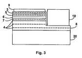
- FIG. 3is a cross sectional view of a III-nitride flip chip LED according to an embodiment of the invention.
- FIGS. 4A and 4Bare a plan view and a cross sectional view of a contacting scheme for a large junction flip chip LED.
- FIGS. 5A and 5Bare a plan view and a cross sectional view of a contact scheme for a small junction flip chip LED.
- FIG. 6is an exploded view of a packaged semiconductor light emitting device.
- One approach to improving current spreading in III-phosphide devices in particularis to increase the thickness of the epitaxial layers between the contacts. Thick epitaxial layers generally increase the cost of producing a device and the amount of light lost to absorption. In addition, in a flip chip device, the need to etch to expose portions of buried layers in order to form contacts limits the thickness with which certain device layers can be grown.
- a III-phosphide flip chip deviceincludes one or more highly doped layers.
- the highly doped layersspread current laterally within the device without increasing the thickness of the epitaxial layers in the device.
- FIG. 1Ais a cross sectional view of a III-phosphide flip chip LED.
- the device of FIG. 1Aincludes an active region 6 sandwiched between a p-doped cladding region 5 and an n-doped cladding region 7 .
- the wavelength of light emitted by the active regionmay be controlled by selecting the width and composition of the layers in active region 6 , as is known in the art.
- An example of a suitable active regionincludes 3 or 4 quantum wells separated by barrier layers.
- n-contact layer 8separates n-contact 10 from the n-doped cladding region 7 .
- a p-contact 9is formed on a p-doped current spreading layer 3 .
- Lightis extracted from the device through an undoped, transparent GaP window layer 1 .
- the table belowgives examples of the thickness, composition, and dopant appropriate for each of layers 3 , 5 , 6 , 7 , and 8 .
- P-doped current1–10 micron thick layer of Mg doped GaP spreading region 3 P-doped cladding 0.5–2 micron thick layer of Mg doped AlInP region 5 Quantum wells of active 80–300 angstrom thick layers of undoped region 6 InGaP Barrier layers of active 100–150 angstrom thick layers of undoped region 6 (Al x Ga 1 ⁇ x ) 0.5 In 0.5 P, x ⁇ 0.65 N-doped cladding 0.5–2 micron thick layer of Te doped AlInP region 7 N-doped contact region 8 500 angstrom thick layer of Te doped GaInP The characteristics given below for each layer are examples and are not meant to be limiting.
- p- and n-type dopantssuch as Zn or Si
- Zn or Sip- and n-type dopants
- More information on selecting the appropriate characteristics of the layers of the devicemay be found in chapters 1–3 of Semiconductors and Semimetals, Volume 64, Electroluminescence I, Academic Press, San Francisco, 2000, Gerd Mueller, ed., which is incorporated herein by reference.
- FIG. 1Billustrates an example of a multilayer p-contact 9 .
- a layer of Au—Zn alloy 9 Ais formed adjacent to current spreading layer 3 , in order to provide ohmic contact to the semiconductor layer.
- Au—Zn layer 9 Amay be protected by an optional guard metal layer 9 B of, for example, a sandwich of TiW, TiW:N, and TiW.
- a thick contact layer 9 C, such as gold,is then formed over guard layer 9 B.
- the ohmic layer 9 A and guard layer 9 Bmay cover all or just a portion of the semiconductor layer 3 on which p-contact 9 is formed.
- a multilayer n-contact 10may have a similar structure, as illustrated in FIG. 1C .
- a layer of Au—Ge alloy 10 Ais fanned adjacent to contact layer 8 , in order to provide ohmic contact to the semiconductor layer.
- Au—Ge layer 10 Amay be protected by an optional guard metal layer 10 B of, for example, a sandwich of TiW, TiW:N, and TiW.
- a thick reflective layer 10 C of Auis deposited over layers 10 A and 10 B.
- Ohmic layer 10 Ais generally not very reflective, and is thus often formed as dots (as in FIG. 1C ) or thin stripes that cover a small fraction of the semiconductor layer 8 on which n-contact 10 is formed.
- Heavily doped layers 4may be included in one or more of p-doped contact layer 3 , p-doped cladding layer 5 , and n-doped cladding layer 7 .
- Heavily doped layers 4are formed in regions of the device that may benefit from additional current spreading.
- p-contact 9does not directly overlie the active region, thus current is required to spread from p-contact 9 to the active region. Accordingly, the p-type side of active region 6 may benefit from additional current spreading and may thus include heavily doped layers 4 .
- n-contact 10is a sheet contact, n-contact 10 overlies the entire active region and additional current spreading is not required on the n-type side of active region 6 . If n-contact 10 includes small regions of ohmic layers 10 A and a large reflective sheet 10 G as illustrated in FIG. 1C , current is required to spread from ohmic contact regions 10 A to the areas of semiconductor layer 8 under reflective sheet 10 C without an ohmic contact region 10 A. In such devices, the n-type side of active region 6 may benefit from additional current spreading and may thus include heavily doped layers 4 .
- Highly doped layers 4are doped with the same conductivity type as the region in which they are formed. For example, highly doped layers 4 within n-type regions of the device are n-type, and highly doped regions 4 within p-type regions are p-type. Typically, highly doped layers 4 are doped with the same dopant species as the surrounding region, though this is not required. Highly doped layers 4 may be doped to a concentration of about 5 ⁇ 10 18 to about 1 ⁇ 10 19 cm ⁇ 3 . In contrast, n-doped cladding region 7 , p-doped cladding region 5 , and p-doped current spreading layer 3 are usually doped to a concentration of about 5 ⁇ 10 17 to about 1 ⁇ 10 18 cm ⁇ 3 .
- highly doped layers 4Due to the high dopant concentration, highly doped layers 4 will tend to absorb light. Accordingly, highly doped layers 4 are usually thin, for example between about 10 and 100 nm thick, and positioned as far from the active region of the device as possible. Multiple highly doped layers 4 may be formed in a single region. In such embodiments, the highly doped layers are usually spaced at least 10 nm apart and the total thickness of all the highly doped layers is between about 100 and about 500 nm.
- highly doped layers 4are the same composition as the regions in which they are disposed.
- highly doped layers 4are quaternary AlInGaP layer having a lower band gap than the regions in which they are disposed, for example (Al x Ga 1-x ) 0.5 In 0.5 P where 0.2 ⁇ x ⁇ 0.7.
- the band gap of a materialthe more highly the material can be doped without sacrificing crystal quality, thus the use of quaternary alloys for heavily doped layers 4 may permit these layers to be more heavily doped.
- the small regions of lower band gap created by the quaternary heavily doped layersmay further encourage lateral current spreading by creating vertical potential barriers.
- FIG. 2illustrates a portion of an energy band diagram for an example of a III-phosphide device incorporating heavily doped layers.
- Each of cladding layers 5 and 7includes four heavily doped layers 4 .
- Cladding layers 5 and 7each have a total thickness of about one micron.
- Heavily doped layers 4are each about 50 nm thick, and separated by about 100 nm. Because of the absorptive nature of heavily doped layers 4 , these layers are located in the portions of cladding layers 5 and 7 furthest from active region 6 .
- Heavily doped layersare (Al 0.65 Ga 0.35 ) 0.5 In 0.5 P doped to a concentration of about 5 ⁇ 10 18 cm ⁇ 3 .
- FIG. 3is a cross sectional view of a III-nitride flip chip device including heavily doped layers.
- an n-contact layer 8is grown over a growth substrate 20 and optional nucleation layers (not shown), followed by an n-type cladding layer 7 , active region 6 , p-type cladding layer 5 , and p-type contact layer 3 .
- the wavelength of light emitted by the active regionmay be controlled by selecting the width and composition of the layers in active region 6 , as is known in the art.
- An example of a suitable active regionincludes 3 or 4 quantum wells separated by barrier layers.
- N-contact 10is formed on a portion of n-contact layer 8 exposed by etching.
- a p-contact 9is formed on p-doped contact layer 3 . Both n-contact 10 and p-contact 9 are reflective and light is extracted from the device through substrate 20 .
- the table belowgives examples of the thickness, composition, and dopant appropriate for each of layers 3 , 5 , 6 , 7 , and 8 .
- P-doped contact region 30.3–0.7 micron thick layer of Mg doped GaN P-doped cladding 0.05–0.25 micron thick layer of Mg doped region 5 AlGaN Quantum wells of active 100–150 angstrom thick layers of undoped region 6 InGaN or AlInGaN Barrier layers of active 50–150 angstrom thick layers of undoped region 6 GaN or InGaN N-doped cladding region 2–6 micron thick layer of Si doped GaN 7 and contact region 8
- the characteristics given below for each layerare examples and are not meant to be limiting.
- heavily doped layers 4may be formed in one or more of p-doped contact layer 3 , p-doped cladding region 5 , n-doped cladding region 7 , and n-doped contact layer 8 .
- p-contactis usually a sheet contact which provides sufficient current spreading on the p-type side of active region 6 . Accordingly, in III-nitride devices, heavily doped layers 4 are often formed on the n-type side of active region 6 only. Heavily doped layers 4 in FIG.
- GaN layersmay be GaN layers, quaternary AlInGaN layers, or may be layers of the same composition as the region in which they are located. Heavily doped layers may have the same thickness, location relative to the active region, and dopant concentration as described above in the text accompanying FIG. 1A .
- FIGS. 4A and 4Billustrate an arrangement of contacts 9 and 10 for a large junction device (that is, a device having an area greater than about 400 ⁇ 400 ⁇ m 2 ) according to FIG. 1A or 3 .
- FIG. 4Ais a plan view and FIG. 4B is a cross section taken along line DD.
- Layers 19include layers 1 , 3 , 4 , 5 , 6 , 7 , and 8 of FIG. 1A or layers 20 , 7 , 8 , 6 , 5 , 3 , and 4 of FIG. 3 .
- the active regionis divided into four isolated regions, in order to minimize the distance between the p- and n-contacts.
- p-contact 9 in the device of FIG. 1A , and n-contact 10 in the device of FIG. 3surrounds and interposes the four regions.
- N-contacts 10 in the device of FIG. 1A , and p-contacts 9 in the device of FIG. 3are formed on the four active regions.
- P- and n-contacts 9 and 10are electrically isolated from each other by air or by optional insulating layer 22 .
- Six submount connections 23 and sixteen submount connections 24are deposited on the p- and n-contacts to form a surface suitable for connecting the device to a submount.
- the submountis often a silicon integrated circuit attached to the device by solder joints.
- the p- and n-submount connectionsmay be, for example, solderable metals.
- the deviceis connected to the submount by gold bonds, cold welding, or thermocompression bonding.
- FIGS. 5A and 5Billustrate an arrangement of contacts 9 and 10 for a small junction device (that is, a device having an area less than about 400 ⁇ 400 ⁇ m 2 ) according to FIG. 1A or 3 .
- FIG. 5Ais a plan view and FIG. 5B is a cross section taken along line CC.
- Layers 19include layers 1 , 3 , 4 , 5 , 6 , 7 , and 8 of FIG. 1A or layers 20 , 7 , 8 , 6 , 5 , 3 , and 4 of FIG. 3 .
- the device shown in FIGS. 5A and 5Bhas a single via 21 etched down to a layer of the epitaxial structure below the active region.
- n-contact 10 in the device of FIG. 3is deposited in via 21 .
- Via 21is located at the center of the device to provide uniform current and light emission.
- An n-contact 10 in the device of FIG. 1A and a p-contact 9 in the device of FIG. 3surrounds the via and provides electrical contact to the other side of the active region of the epitaxial structure.
- the p- and n-contactsare separated and electrically isolated by one or more dielectric layers 22 , or by air.
- Two submount connections 24 and one submount connection 23are disposed on p- and n-contacts 9 and 10 .
- Submount connection 23may be located anywhere within the region surrounded by insulating layer 22 and need not necessarily be located directly over via 21 .
- submount connections 24may be located anywhere in the region outside insulating layer 22 .
- the connection of the device to a submountis not limited by the shape or placement of p-contact 9 and n-contact 10 .
- FIG. 6is an exploded view of a packaged light emitting device.
- a heat-sinking slug 100is placed into an insert-molded leadframe.
- the insert-molded leadframeis, for example, a filled plastic material 105 molded around a metal frame 106 that provides an electrical path.
- Slug 100may include an optional reflector cup 102 .
- the light emitting device die 104which may be any of the devices described above, is mounted directly or indirectly via a thermally conducting submount 103 to slug 100 .
- a cover 108which may be an optical lens, may be added.
Landscapes
- Led Devices (AREA)
Abstract
Description
| P-doped current | 1–10 micron thick layer of Mg doped GaP |
| spreading region 3 | |
| P-doped cladding | 0.5–2 micron thick layer of Mg doped |
| region | |
| 5 | |
| Quantum wells of active | 80–300 angstrom thick layers of |
| region | |
| 6 | InGaP |
| Barrier layers of active | 100–150 angstrom thick layers of undoped |
| region 6 | (AlxGa1−x)0.5In0.5P, x~0.65 |
| N-doped cladding | 0.5–2 micron thick layer of Te doped AlInP |
| region 7 | |
| N-doped | 500 angstrom thick layer of Te doped GaInP |
The characteristics given below for each layer are examples and are not meant to be limiting. For example, other p- and n-type dopants, such as Zn or Si, may be used. More information on selecting the appropriate characteristics of the layers of the device may be found in
| P-doped | 0.3–0.7 micron thick layer of Mg doped GaN |
| P-doped cladding | 0.05–0.25 micron thick layer of Mg doped |
| AlGaN | |
| Quantum wells of active | 100–150 angstrom thick layers of |
| region | |
| 6 | InGaN or AlInGaN |
| Barrier layers of active | 50–150 angstrom thick layers of |
| region | |
| 6 | GaN or InGaN |
| N-doped cladding region | 2–6 micron thick layer of Si doped |
| 7 and contact | |
The characteristics given below for each layer are examples and are not meant to be limiting.
Claims (18)
Priority Applications (4)
| Application Number | Priority Date | Filing Date | Title |
|---|---|---|---|
| US10/766,277US7026653B2 (en) | 2004-01-27 | 2004-01-27 | Semiconductor light emitting devices including current spreading layers |
| EP05100249.1AEP1560275B1 (en) | 2004-01-27 | 2005-01-17 | Semiconductor light emitting devices including current spreading layers |
| TW094102019ATWI430468B (en) | 2004-01-27 | 2005-01-24 | Semiconductor light emitting device including current spreading layer |
| JP2005018042AJP2005217406A (en) | 2004-01-27 | 2005-01-26 | Semiconductor light emitting device including current spreading layer |
Applications Claiming Priority (1)
| Application Number | Priority Date | Filing Date | Title |
|---|---|---|---|
| US10/766,277US7026653B2 (en) | 2004-01-27 | 2004-01-27 | Semiconductor light emitting devices including current spreading layers |
Publications (2)
| Publication Number | Publication Date |
|---|---|
| US20050161679A1 US20050161679A1 (en) | 2005-07-28 |
| US7026653B2true US7026653B2 (en) | 2006-04-11 |
Family
ID=34654329
Family Applications (1)
| Application Number | Title | Priority Date | Filing Date |
|---|---|---|---|
| US10/766,277Expired - LifetimeUS7026653B2 (en) | 2004-01-27 | 2004-01-27 | Semiconductor light emitting devices including current spreading layers |
Country Status (4)
| Country | Link |
|---|---|
| US (1) | US7026653B2 (en) |
| EP (1) | EP1560275B1 (en) |
| JP (1) | JP2005217406A (en) |
| TW (1) | TWI430468B (en) |
Cited By (45)
| Publication number | Priority date | Publication date | Assignee | Title |
|---|---|---|---|---|
| US20060268954A1 (en)* | 2004-08-31 | 2006-11-30 | Johnson Ralph H | Light emitting semiconductor device having an electrical confinement barrier near the active region |
| WO2008016828A3 (en)* | 2006-07-31 | 2008-04-24 | Finisar Corp | Efficient carrier injection in a semiconductor device |
| US20090267083A1 (en)* | 2008-04-28 | 2009-10-29 | Jie Cui | Trenched substrate for crystal growth and wafer bonding |
| US7772604B2 (en) | 2006-01-05 | 2010-08-10 | Illumitex | Separate optical device for directing light from an LED |
| US7789531B2 (en) | 2006-10-02 | 2010-09-07 | Illumitex, Inc. | LED system and method |
| US7829358B2 (en) | 2008-02-08 | 2010-11-09 | Illumitex, Inc. | System and method for emitter layer shaping |
| US20100314649A1 (en)* | 2009-06-10 | 2010-12-16 | Bridgelux, Inc. | Thin-film led with p and n contacts electricall isolated from the substrate |
| US20110050681A1 (en)* | 2009-08-27 | 2011-03-03 | Novatek Microelectronics Corp. | Low voltage differential signal output stage |
| US20110121357A1 (en)* | 2009-11-25 | 2011-05-26 | Steven Lester | LED with Improved Injection Efficiency |
| US20110198664A1 (en)* | 2010-02-12 | 2011-08-18 | Dae Sung Kang | Light emitting device and light emitting device package including the same |
| US8031752B1 (en) | 2007-04-16 | 2011-10-04 | Finisar Corporation | VCSEL optimized for high speed data |
| US8115217B2 (en) | 2008-12-11 | 2012-02-14 | Illumitex, Inc. | Systems and methods for packaging light-emitting diode devices |
| US8304976B2 (en) | 2009-06-30 | 2012-11-06 | 3M Innovative Properties Company | Electroluminescent devices with color adjustment based on current crowding |
| US8395165B2 (en) | 2011-07-08 | 2013-03-12 | Bridelux, Inc. | Laterally contacted blue LED with superlattice current spreading layer |
| CN101515613B (en)* | 2008-02-19 | 2013-04-03 | 晶元光电股份有限公司 | semiconductor element |
| US8449128B2 (en) | 2009-08-20 | 2013-05-28 | Illumitex, Inc. | System and method for a lens and phosphor layer |
| US8541803B2 (en) | 2009-05-05 | 2013-09-24 | 3M Innovative Properties Company | Cadmium-free re-emitting semiconductor construction |
| US8552465B2 (en) | 2011-11-09 | 2013-10-08 | Toshiba Techno Center Inc. | Method for reducing stress in epitaxial growth |
| US8558247B2 (en) | 2011-09-06 | 2013-10-15 | Toshiba Techno Center Inc. | GaN LEDs with improved area and method for making the same |
| US8564010B2 (en) | 2011-08-04 | 2013-10-22 | Toshiba Techno Center Inc. | Distributed current blocking structures for light emitting diodes |
| US8581267B2 (en) | 2011-11-09 | 2013-11-12 | Toshiba Techno Center Inc. | Series connected segmented LED |
| US8585253B2 (en) | 2009-08-20 | 2013-11-19 | Illumitex, Inc. | System and method for color mixing lens array |
| US8624482B2 (en) | 2011-09-01 | 2014-01-07 | Toshiba Techno Center Inc. | Distributed bragg reflector for reflecting light of multiple wavelengths from an LED |
| US8629611B2 (en) | 2009-06-30 | 2014-01-14 | 3M Innovative Properties Company | White light electroluminescent devices with adjustable color temperature |
| US8664679B2 (en) | 2011-09-29 | 2014-03-04 | Toshiba Techno Center Inc. | Light emitting devices having light coupling layers with recessed electrodes |
| US8669585B1 (en) | 2011-09-03 | 2014-03-11 | Toshiba Techno Center Inc. | LED that has bounding silicon-doped regions on either side of a strain release layer |
| US8686430B2 (en) | 2011-09-07 | 2014-04-01 | Toshiba Techno Center Inc. | Buffer layer for GaN-on-Si LED |
| US8698163B2 (en) | 2011-09-29 | 2014-04-15 | Toshiba Techno Center Inc. | P-type doping layers for use with light emitting devices |
| US8785904B2 (en) | 2011-04-20 | 2014-07-22 | Invenlux Corporation | Light-emitting device with low forward voltage and method for fabricating the same |
| US8853668B2 (en) | 2011-09-29 | 2014-10-07 | Kabushiki Kaisha Toshiba | Light emitting regions for use with light emitting devices |
| US8865565B2 (en) | 2011-08-02 | 2014-10-21 | Kabushiki Kaisha Toshiba | LED having a low defect N-type layer that has grown on a silicon substrate |
| US8916906B2 (en) | 2011-07-29 | 2014-12-23 | Kabushiki Kaisha Toshiba | Boron-containing buffer layer for growing gallium nitride on silicon |
| US8994071B2 (en) | 2009-05-05 | 2015-03-31 | 3M Innovative Properties Company | Semiconductor devices grown on indium-containing substrates utilizing indium depletion mechanisms |
| US9012939B2 (en) | 2011-08-02 | 2015-04-21 | Kabushiki Kaisha Toshiba | N-type gallium-nitride layer having multiple conductive intervening layers |
| US9012921B2 (en) | 2011-09-29 | 2015-04-21 | Kabushiki Kaisha Toshiba | Light emitting devices having light coupling layers |
| US9130068B2 (en) | 2011-09-29 | 2015-09-08 | Manutius Ip, Inc. | Light emitting devices having dislocation density maintaining buffer layers |
| US9142743B2 (en) | 2011-08-02 | 2015-09-22 | Kabushiki Kaisha Toshiba | High temperature gold-free wafer bonding for light emitting diodes |
| US9159869B2 (en) | 2011-08-03 | 2015-10-13 | Kabushiki Kaisha Toshiba | LED on silicon substrate using zinc-sulfide as buffer layer |
| US9178114B2 (en) | 2011-09-29 | 2015-11-03 | Manutius Ip, Inc. | P-type doping layers for use with light emitting devices |
| US9184344B2 (en) | 2012-01-25 | 2015-11-10 | Invenlux Limited | Lighting-emitting device with nanostructured layer and method for fabricating the same |
| US9293622B2 (en) | 2009-05-05 | 2016-03-22 | 3M Innovative Properties Company | Re-emitting semiconductor carrier devices for use with LEDs and methods of manufacture |
| US9330911B2 (en) | 2011-08-22 | 2016-05-03 | Invenlux Limited | Light emitting device having group III-nitride current spreading layer doped with transition metal or comprising transition metal nitride |
| US9343641B2 (en) | 2011-08-02 | 2016-05-17 | Manutius Ip, Inc. | Non-reactive barrier metal for eutectic bonding process |
| US9362445B2 (en) | 2012-06-20 | 2016-06-07 | Nanyang Technological University | Light-emitting device |
| US9617656B2 (en) | 2011-07-25 | 2017-04-11 | Toshiba Corporation | Nucleation of aluminum nitride on a silicon substrate using an ammonia preflow |
Families Citing this family (7)
| Publication number | Priority date | Publication date | Assignee | Title |
|---|---|---|---|---|
| JP2007149791A (en)* | 2005-11-24 | 2007-06-14 | Univ Meijo | Semiconductor light emitting device and method for producing semiconductor light emitting device |
| DE102006034847A1 (en)* | 2006-04-27 | 2007-10-31 | Osram Opto Semiconductors Gmbh | Opto-electronic semiconductor chip e.g. light emitting diode chip, has contact layer, where electrical contact resistance of contact layer to connection layer is smaller than contact layer to barrier layer |
| US20080042145A1 (en)* | 2006-08-18 | 2008-02-21 | Helmut Hagleitner | Diffusion barrier for light emitting diodes |
| CN102334204B (en) | 2010-01-06 | 2013-11-20 | 松下电器产业株式会社 | Nitride semiconductor light-emitting element and process for production thereof |
| CN105870280B (en) | 2015-01-21 | 2019-07-09 | 展晶科技(深圳)有限公司 | LED crystal particle |
| CN105742427B (en)* | 2016-04-11 | 2017-12-22 | 天津三安光电有限公司 | Light emitting diode and preparation method thereof |
| CN105720160B (en)* | 2016-04-27 | 2018-01-12 | 天津三安光电有限公司 | Light emitting diode and preparation method thereof |
Citations (13)
| Publication number | Priority date | Publication date | Assignee | Title |
|---|---|---|---|---|
| US4371968A (en)* | 1981-07-01 | 1983-02-01 | The United States Of America As Represented By The Secretary Of The Army | Monolithic injection laser arrays formed by crystal regrowth techniques |
| US5226053A (en)* | 1991-12-27 | 1993-07-06 | At&T Bell Laboratories | Light emitting diode |
| US5498883A (en)* | 1992-08-05 | 1996-03-12 | Motorola, Inc. | Superluminescent edge emitting device with apparent vertical light emission and method of making |
| US5614734A (en)* | 1995-03-15 | 1997-03-25 | Yale University | High efficency LED structure |
| US5818859A (en)* | 1996-06-27 | 1998-10-06 | Minnesota Mining And Manufacturing Company | Be-containing II-VI blue-green laser diodes |
| US6015719A (en)* | 1997-10-24 | 2000-01-18 | Hewlett-Packard Company | Transparent substrate light emitting diodes with directed light output |
| US6121638A (en)* | 1995-09-12 | 2000-09-19 | Kabushiki Kaisha Toshiba | Multi-layer structured nitride-based semiconductor devices |
| US6222205B1 (en)* | 1997-09-20 | 2001-04-24 | Vishay Semiconductor Gmbh | Layered semiconductor structure for lateral current spreading, and light emitting diode including such a current spreading structure |
| US20030089906A1 (en)* | 2001-11-13 | 2003-05-15 | Matsushita Electric Industrial Co., Ltd. | Semiconductor device and method for fabricating the same |
| US20030205717A1 (en)* | 2001-03-01 | 2003-11-06 | Reena Khare | Increasing the brightness of III-Nitride light emitting devices |
| US6720570B2 (en)* | 2002-04-17 | 2004-04-13 | Tekcore Co., Ltd. | Gallium nitride-based semiconductor light emitting device |
| US6829271B2 (en)* | 1999-02-15 | 2004-12-07 | Ricoh Company, Ltd. | Light-emitting semiconductor device producing red wavelength optical radiation |
| US20050045893A1 (en)* | 2003-08-28 | 2005-03-03 | Ludowise Michael J. | Resonant cavity light emitting device |
Family Cites Families (19)
| Publication number | Priority date | Publication date | Assignee | Title |
|---|---|---|---|---|
| JP3264563B2 (en)* | 1993-03-15 | 2002-03-11 | 株式会社東芝 | Semiconductor light emitting device and method of manufacturing the same |
| JP3237972B2 (en)* | 1993-09-10 | 2001-12-10 | 株式会社東芝 | Semiconductor light emitting device |
| JP3195194B2 (en)* | 1995-05-26 | 2001-08-06 | シャープ株式会社 | Semiconductor light emitting device and method of manufacturing the same |
| JP3374737B2 (en)* | 1997-01-09 | 2003-02-10 | 日亜化学工業株式会社 | Nitride semiconductor device |
| US6107648A (en)* | 1997-03-13 | 2000-08-22 | Rohm Co., Ltd. | Semiconductor light emitting device having a structure which relieves lattice mismatch |
| JP3488597B2 (en)* | 1997-07-14 | 2004-01-19 | 株式会社東芝 | Gallium nitride based compound semiconductor device |
| JP3680558B2 (en)* | 1998-05-25 | 2005-08-10 | 日亜化学工業株式会社 | Nitride semiconductor device |
| JP2000082841A (en)* | 1998-06-22 | 2000-03-21 | Hitachi Cable Ltd | Epitaxial wafer and method for manufacturing the same |
| JP2000031591A (en)* | 1998-07-08 | 2000-01-28 | Toshiba Corp | Semiconductor light emitting device |
| JP3656456B2 (en)* | 1999-04-21 | 2005-06-08 | 日亜化学工業株式会社 | Nitride semiconductor device |
| JP2001007445A (en)* | 1999-06-25 | 2001-01-12 | Hitachi Cable Ltd | AlGaInP-based light emitting device and epitaxial wafer for light emitting device |
| JP3609661B2 (en)* | 1999-08-19 | 2005-01-12 | 株式会社東芝 | Semiconductor light emitting device |
| US6898215B2 (en)* | 2001-04-11 | 2005-05-24 | Optical Communication Products, Inc. | Long wavelength vertical cavity surface emitting laser |
| JP2003046127A (en)* | 2001-05-23 | 2003-02-14 | Sanyo Electric Co Ltd | Nitride semiconductor light-emitting element |
| JP2003086513A (en)* | 2001-06-26 | 2003-03-20 | Fuji Photo Film Co Ltd | Method for manufacturing substrate for semiconductor device, and substrate for semiconductor device and semiconductor device |
| KR100889842B1 (en)* | 2001-07-04 | 2009-03-20 | 니치아 카가쿠 고교 가부시키가이샤 | Nitride Semiconductor Devices |
| JP4250909B2 (en)* | 2002-05-20 | 2009-04-08 | ソニー株式会社 | Semiconductor element separation method and transfer method |
| US20030230977A1 (en)* | 2002-06-12 | 2003-12-18 | Epstein Howard C. | Semiconductor light emitting device with fluoropolymer lens |
| JP4254373B2 (en)* | 2003-06-24 | 2009-04-15 | 日亜化学工業株式会社 | Nitride semiconductor device |
- 2004
- 2004-01-27USUS10/766,277patent/US7026653B2/ennot_activeExpired - Lifetime
- 2005
- 2005-01-17EPEP05100249.1Apatent/EP1560275B1/ennot_activeExpired - Lifetime
- 2005-01-24TWTW094102019Apatent/TWI430468B/ennot_activeIP Right Cessation
- 2005-01-26JPJP2005018042Apatent/JP2005217406A/enactivePending
Patent Citations (13)
| Publication number | Priority date | Publication date | Assignee | Title |
|---|---|---|---|---|
| US4371968A (en)* | 1981-07-01 | 1983-02-01 | The United States Of America As Represented By The Secretary Of The Army | Monolithic injection laser arrays formed by crystal regrowth techniques |
| US5226053A (en)* | 1991-12-27 | 1993-07-06 | At&T Bell Laboratories | Light emitting diode |
| US5498883A (en)* | 1992-08-05 | 1996-03-12 | Motorola, Inc. | Superluminescent edge emitting device with apparent vertical light emission and method of making |
| US5614734A (en)* | 1995-03-15 | 1997-03-25 | Yale University | High efficency LED structure |
| US6121638A (en)* | 1995-09-12 | 2000-09-19 | Kabushiki Kaisha Toshiba | Multi-layer structured nitride-based semiconductor devices |
| US5818859A (en)* | 1996-06-27 | 1998-10-06 | Minnesota Mining And Manufacturing Company | Be-containing II-VI blue-green laser diodes |
| US6222205B1 (en)* | 1997-09-20 | 2001-04-24 | Vishay Semiconductor Gmbh | Layered semiconductor structure for lateral current spreading, and light emitting diode including such a current spreading structure |
| US6015719A (en)* | 1997-10-24 | 2000-01-18 | Hewlett-Packard Company | Transparent substrate light emitting diodes with directed light output |
| US6829271B2 (en)* | 1999-02-15 | 2004-12-07 | Ricoh Company, Ltd. | Light-emitting semiconductor device producing red wavelength optical radiation |
| US20030205717A1 (en)* | 2001-03-01 | 2003-11-06 | Reena Khare | Increasing the brightness of III-Nitride light emitting devices |
| US20030089906A1 (en)* | 2001-11-13 | 2003-05-15 | Matsushita Electric Industrial Co., Ltd. | Semiconductor device and method for fabricating the same |
| US6720570B2 (en)* | 2002-04-17 | 2004-04-13 | Tekcore Co., Ltd. | Gallium nitride-based semiconductor light emitting device |
| US20050045893A1 (en)* | 2003-08-28 | 2005-03-03 | Ludowise Michael J. | Resonant cavity light emitting device |
Non-Patent Citations (1)
| Title |
|---|
| D. A. Vanderwater et al., "High-Brightness AlGaInP Light Emitting Diodes", Proceedings of the IEEE, vol. 85, No. 11, Nov. 1997, pp. 1752-1764. |
Cited By (73)
| Publication number | Priority date | Publication date | Assignee | Title |
|---|---|---|---|---|
| US20060268954A1 (en)* | 2004-08-31 | 2006-11-30 | Johnson Ralph H | Light emitting semiconductor device having an electrical confinement barrier near the active region |
| US7920612B2 (en) | 2004-08-31 | 2011-04-05 | Finisar Corporation | Light emitting semiconductor device having an electrical confinement barrier near the active region |
| US9574743B2 (en) | 2006-01-05 | 2017-02-21 | Illumitex, Inc. | Separate optical device for directing light from an LED |
| US7772604B2 (en) | 2006-01-05 | 2010-08-10 | Illumitex | Separate optical device for directing light from an LED |
| US8896003B2 (en) | 2006-01-05 | 2014-11-25 | Illumitex, Inc. | Separate optical device for directing light from an LED |
| US7968896B2 (en) | 2006-01-05 | 2011-06-28 | Illumitex, Inc. | Separate optical device for directing light from an LED |
| WO2008016828A3 (en)* | 2006-07-31 | 2008-04-24 | Finisar Corp | Efficient carrier injection in a semiconductor device |
| CN101162752B (en)* | 2006-07-31 | 2010-06-23 | 菲尼萨公司 | Efficient carrier injection in a semiconductor device |
| US7829912B2 (en) | 2006-07-31 | 2010-11-09 | Finisar Corporation | Efficient carrier injection in a semiconductor device |
| US7789531B2 (en) | 2006-10-02 | 2010-09-07 | Illumitex, Inc. | LED system and method |
| US8087960B2 (en) | 2006-10-02 | 2012-01-03 | Illumitex, Inc. | LED system and method |
| US8031752B1 (en) | 2007-04-16 | 2011-10-04 | Finisar Corporation | VCSEL optimized for high speed data |
| US7829358B2 (en) | 2008-02-08 | 2010-11-09 | Illumitex, Inc. | System and method for emitter layer shaping |
| US8263993B2 (en) | 2008-02-08 | 2012-09-11 | Illumitex, Inc. | System and method for emitter layer shaping |
| CN101515613B (en)* | 2008-02-19 | 2013-04-03 | 晶元光电股份有限公司 | semiconductor element |
| US8664747B2 (en) | 2008-04-28 | 2014-03-04 | Toshiba Techno Center Inc. | Trenched substrate for crystal growth and wafer bonding |
| US20090267083A1 (en)* | 2008-04-28 | 2009-10-29 | Jie Cui | Trenched substrate for crystal growth and wafer bonding |
| US8115217B2 (en) | 2008-12-11 | 2012-02-14 | Illumitex, Inc. | Systems and methods for packaging light-emitting diode devices |
| US9293622B2 (en) | 2009-05-05 | 2016-03-22 | 3M Innovative Properties Company | Re-emitting semiconductor carrier devices for use with LEDs and methods of manufacture |
| US8994071B2 (en) | 2009-05-05 | 2015-03-31 | 3M Innovative Properties Company | Semiconductor devices grown on indium-containing substrates utilizing indium depletion mechanisms |
| US8541803B2 (en) | 2009-05-05 | 2013-09-24 | 3M Innovative Properties Company | Cadmium-free re-emitting semiconductor construction |
| US20100314649A1 (en)* | 2009-06-10 | 2010-12-16 | Bridgelux, Inc. | Thin-film led with p and n contacts electricall isolated from the substrate |
| US8871539B2 (en) | 2009-06-10 | 2014-10-28 | Kabushiki Kaisha Toshiba | Thin-film LED with P and N contacts electrically isolated from the substrate |
| US8536601B2 (en) | 2009-06-10 | 2013-09-17 | Toshiba Techno Center, Inc. | Thin-film LED with P and N contacts electrically isolated from the substrate |
| US8546832B2 (en) | 2009-06-10 | 2013-10-01 | Toshiba Techno Center Inc. | Thin-film LED with p and n contacts electrically isolated from the substrate |
| US9142742B2 (en) | 2009-06-10 | 2015-09-22 | Kabushiki Kaisha Toshiba | Thin-film LED with P and N contacts electrically isolated from the substrate |
| US20100314651A1 (en)* | 2009-06-10 | 2010-12-16 | Bridgelux, Inc. | Thin-film led with p and n contacts electrically isolated from the substrate |
| US8304976B2 (en) | 2009-06-30 | 2012-11-06 | 3M Innovative Properties Company | Electroluminescent devices with color adjustment based on current crowding |
| US8629611B2 (en) | 2009-06-30 | 2014-01-14 | 3M Innovative Properties Company | White light electroluminescent devices with adjustable color temperature |
| US8449128B2 (en) | 2009-08-20 | 2013-05-28 | Illumitex, Inc. | System and method for a lens and phosphor layer |
| US9086211B2 (en) | 2009-08-20 | 2015-07-21 | Illumitex, Inc. | System and method for color mixing lens array |
| US8585253B2 (en) | 2009-08-20 | 2013-11-19 | Illumitex, Inc. | System and method for color mixing lens array |
| US20110050681A1 (en)* | 2009-08-27 | 2011-03-03 | Novatek Microelectronics Corp. | Low voltage differential signal output stage |
| US20110121357A1 (en)* | 2009-11-25 | 2011-05-26 | Steven Lester | LED with Improved Injection Efficiency |
| US8525221B2 (en) | 2009-11-25 | 2013-09-03 | Toshiba Techno Center, Inc. | LED with improved injection efficiency |
| US9012953B2 (en) | 2009-11-25 | 2015-04-21 | Kabushiki Kaisha Toshiba | LED with improved injection efficiency |
| US8684749B2 (en) | 2009-11-25 | 2014-04-01 | Toshiba Techno Center Inc. | LED with improved injection efficiency |
| US20110198664A1 (en)* | 2010-02-12 | 2011-08-18 | Dae Sung Kang | Light emitting device and light emitting device package including the same |
| US8860077B2 (en)* | 2010-02-12 | 2014-10-14 | Lg Innotek Co., Ltd. | Light emitting device and light emitting device package including the same |
| US8785904B2 (en) | 2011-04-20 | 2014-07-22 | Invenlux Corporation | Light-emitting device with low forward voltage and method for fabricating the same |
| US8395165B2 (en) | 2011-07-08 | 2013-03-12 | Bridelux, Inc. | Laterally contacted blue LED with superlattice current spreading layer |
| US9617656B2 (en) | 2011-07-25 | 2017-04-11 | Toshiba Corporation | Nucleation of aluminum nitride on a silicon substrate using an ammonia preflow |
| US10174439B2 (en) | 2011-07-25 | 2019-01-08 | Samsung Electronics Co., Ltd. | Nucleation of aluminum nitride on a silicon substrate using an ammonia preflow |
| US8916906B2 (en) | 2011-07-29 | 2014-12-23 | Kabushiki Kaisha Toshiba | Boron-containing buffer layer for growing gallium nitride on silicon |
| US8865565B2 (en) | 2011-08-02 | 2014-10-21 | Kabushiki Kaisha Toshiba | LED having a low defect N-type layer that has grown on a silicon substrate |
| US9343641B2 (en) | 2011-08-02 | 2016-05-17 | Manutius Ip, Inc. | Non-reactive barrier metal for eutectic bonding process |
| US9142743B2 (en) | 2011-08-02 | 2015-09-22 | Kabushiki Kaisha Toshiba | High temperature gold-free wafer bonding for light emitting diodes |
| US9012939B2 (en) | 2011-08-02 | 2015-04-21 | Kabushiki Kaisha Toshiba | N-type gallium-nitride layer having multiple conductive intervening layers |
| US9159869B2 (en) | 2011-08-03 | 2015-10-13 | Kabushiki Kaisha Toshiba | LED on silicon substrate using zinc-sulfide as buffer layer |
| US9070833B2 (en) | 2011-08-04 | 2015-06-30 | Kabushiki Kaisha Toshiba | Distributed current blocking structures for light emitting diodes |
| US8564010B2 (en) | 2011-08-04 | 2013-10-22 | Toshiba Techno Center Inc. | Distributed current blocking structures for light emitting diodes |
| US9330911B2 (en) | 2011-08-22 | 2016-05-03 | Invenlux Limited | Light emitting device having group III-nitride current spreading layer doped with transition metal or comprising transition metal nitride |
| US8981410B1 (en) | 2011-09-01 | 2015-03-17 | Kabushiki Kaisha Toshiba | Distributed bragg reflector for reflecting light of multiple wavelengths from an LED |
| US8624482B2 (en) | 2011-09-01 | 2014-01-07 | Toshiba Techno Center Inc. | Distributed bragg reflector for reflecting light of multiple wavelengths from an LED |
| US8669585B1 (en) | 2011-09-03 | 2014-03-11 | Toshiba Techno Center Inc. | LED that has bounding silicon-doped regions on either side of a strain release layer |
| US8994064B2 (en) | 2011-09-03 | 2015-03-31 | Kabushiki Kaisha Toshiba | Led that has bounding silicon-doped regions on either side of a strain release layer |
| US8558247B2 (en) | 2011-09-06 | 2013-10-15 | Toshiba Techno Center Inc. | GaN LEDs with improved area and method for making the same |
| US9018643B2 (en) | 2011-09-06 | 2015-04-28 | Kabushiki Kaisha Toshiba | GaN LEDs with improved area and method for making the same |
| US8686430B2 (en) | 2011-09-07 | 2014-04-01 | Toshiba Techno Center Inc. | Buffer layer for GaN-on-Si LED |
| US8698163B2 (en) | 2011-09-29 | 2014-04-15 | Toshiba Techno Center Inc. | P-type doping layers for use with light emitting devices |
| US9490392B2 (en) | 2011-09-29 | 2016-11-08 | Toshiba Corporation | P-type doping layers for use with light emitting devices |
| US9178114B2 (en) | 2011-09-29 | 2015-11-03 | Manutius Ip, Inc. | P-type doping layers for use with light emitting devices |
| US9012921B2 (en) | 2011-09-29 | 2015-04-21 | Kabushiki Kaisha Toshiba | Light emitting devices having light coupling layers |
| US9130068B2 (en) | 2011-09-29 | 2015-09-08 | Manutius Ip, Inc. | Light emitting devices having dislocation density maintaining buffer layers |
| US9299881B2 (en) | 2011-09-29 | 2016-03-29 | Kabishiki Kaisha Toshiba | Light emitting devices having light coupling layers |
| US8853668B2 (en) | 2011-09-29 | 2014-10-07 | Kabushiki Kaisha Toshiba | Light emitting regions for use with light emitting devices |
| US8664679B2 (en) | 2011-09-29 | 2014-03-04 | Toshiba Techno Center Inc. | Light emitting devices having light coupling layers with recessed electrodes |
| US9391234B2 (en) | 2011-11-09 | 2016-07-12 | Toshiba Corporation | Series connected segmented LED |
| US8581267B2 (en) | 2011-11-09 | 2013-11-12 | Toshiba Techno Center Inc. | Series connected segmented LED |
| US9123853B2 (en) | 2011-11-09 | 2015-09-01 | Manutius Ip, Inc. | Series connected segmented LED |
| US8552465B2 (en) | 2011-11-09 | 2013-10-08 | Toshiba Techno Center Inc. | Method for reducing stress in epitaxial growth |
| US9184344B2 (en) | 2012-01-25 | 2015-11-10 | Invenlux Limited | Lighting-emitting device with nanostructured layer and method for fabricating the same |
| US9362445B2 (en) | 2012-06-20 | 2016-06-07 | Nanyang Technological University | Light-emitting device |
Also Published As
| Publication number | Publication date |
|---|---|
| EP1560275B1 (en) | 2019-03-13 |
| TWI430468B (en) | 2014-03-11 |
| US20050161679A1 (en) | 2005-07-28 |
| EP1560275A3 (en) | 2014-02-26 |
| EP1560275A2 (en) | 2005-08-03 |
| JP2005217406A (en) | 2005-08-11 |
| TW200537711A (en) | 2005-11-16 |
Similar Documents
| Publication | Publication Date | Title |
|---|---|---|
| US7026653B2 (en) | Semiconductor light emitting devices including current spreading layers | |
| US7274040B2 (en) | Contact and omnidirectional reflective mirror for flip chipped light emitting devices | |
| US6828596B2 (en) | Contacting scheme for large and small area semiconductor light emitting flip chip devices | |
| US6977396B2 (en) | High-powered light emitting device with improved thermal properties | |
| US8679869B2 (en) | Contact for a semiconductor light emitting device | |
| US8541807B2 (en) | Semiconductor light emitting device and light emitting apparatus having the same | |
| US6547249B2 (en) | Monolithic series/parallel led arrays formed on highly resistive substrates | |
| US6822991B2 (en) | Light emitting devices including tunnel junctions | |
| US7649193B2 (en) | Semiconductor body and semiconductor chip comprising a semiconductor body | |
| US7019330B2 (en) | Resonant cavity light emitting device | |
| US20050037527A1 (en) | Light emitting element, method of manufacturing the same, and semiconductor device having light emitting element | |
| US8368092B2 (en) | Thin film LED comprising a current-dispersing structure | |
| US11329204B2 (en) | Micro light emitting diode and manufacturing method of micro light emitting diode | |
| US9768368B2 (en) | Side interconnect for light emitting device | |
| KR20120029232A (en) | Light emitting diode | |
| KR102350784B1 (en) | Uv light emitting device and lighting system | |
| KR102299735B1 (en) | Light emitting device and lighting system | |
| KR20120015623A (en) | Light emitting element | |
| KR20120087034A (en) | Light emitting device and light emitting device package | |
| KR20180122884A (en) | Semiconductor device | |
| KR20120047448A (en) | Light emitting device | |
| KR20120011176A (en) | Light emitting element |
Legal Events
| Date | Code | Title | Description |
|---|---|---|---|
| AS | Assignment | Owner name:LUMILEDS LIGHTING U.S., LLC, CALIFORNIA Free format text:ASSIGNMENT OF ASSIGNORS INTEREST;ASSIGNOR:SUN, DECAI;REEL/FRAME:014481/0703 Effective date:20040311 | |
| STCF | Information on status: patent grant | Free format text:PATENTED CASE | |
| CC | Certificate of correction | ||
| REMI | Maintenance fee reminder mailed | ||
| FPAY | Fee payment | Year of fee payment:4 | |
| SULP | Surcharge for late payment | ||
| AS | Assignment | Owner name:PHILIPS LUMILEDS LIGHTING COMPANY LLC, CALIFORNIA Free format text:CHANGE OF NAME;ASSIGNORS:LUMILEDS LIGHTING U.S., LLC;LUMILEDS LIGHTING, U.S., LLC;LUMILEDS LIGHTING, U.S. LLC;AND OTHERS;REEL/FRAME:025850/0770 Effective date:20110211 | |
| FPAY | Fee payment | Year of fee payment:8 | |
| AS | Assignment | Owner name:DEUTSCHE BANK AG NEW YORK BRANCH, AS COLLATERAL AGENT, NEW YORK Free format text:SECURITY INTEREST;ASSIGNOR:LUMILEDS LLC;REEL/FRAME:043108/0001 Effective date:20170630 Owner name:DEUTSCHE BANK AG NEW YORK BRANCH, AS COLLATERAL AG Free format text:SECURITY INTEREST;ASSIGNOR:LUMILEDS LLC;REEL/FRAME:043108/0001 Effective date:20170630 | |
| MAFP | Maintenance fee payment | Free format text:PAYMENT OF MAINTENANCE FEE, 12TH YEAR, LARGE ENTITY (ORIGINAL EVENT CODE: M1553) Year of fee payment:12 | |
| AS | Assignment | Owner name:LUMILEDS LLC, CALIFORNIA Free format text:CHANGE OF NAME;ASSIGNOR:PHILIPS LUMILEDS LIGHTING COMPANY, LLC;REEL/FRAME:046111/0261 Effective date:20150326 | |
| AS | Assignment | Owner name:SOUND POINT AGENCY LLC, NEW YORK Free format text:SECURITY INTEREST;ASSIGNORS:LUMILEDS LLC;LUMILEDS HOLDING B.V.;REEL/FRAME:062299/0338 Effective date:20221230 | |
| AS | Assignment | Owner name:LUMILEDS HOLDING B.V., NETHERLANDS Free format text:RELEASE BY SECURED PARTY;ASSIGNOR:SOUND POINT AGENCY LLC;REEL/FRAME:070046/0001 Effective date:20240731 Owner name:LUMILEDS LLC, CALIFORNIA Free format text:RELEASE BY SECURED PARTY;ASSIGNOR:SOUND POINT AGENCY LLC;REEL/FRAME:070046/0001 Effective date:20240731 | |
| AS | Assignment | Owner name:LUMILEDS SINGAPORE PTE. LTD., SINGAPORE Free format text:ASSIGNMENT OF ASSIGNORS INTEREST;ASSIGNOR:LUMILEDS LLC;REEL/FRAME:071888/0086 Effective date:20250708 |