US7026235B1 - Dual-damascene process and associated floating metal structures - Google Patents
Dual-damascene process and associated floating metal structuresDownload PDFInfo
- Publication number
- US7026235B1 US7026235B1US10/072,164US7216402AUS7026235B1US 7026235 B1US7026235 B1US 7026235B1US 7216402 AUS7216402 AUS 7216402AUS 7026235 B1US7026235 B1US 7026235B1
- Authority
- US
- United States
- Prior art keywords
- layer
- metal
- sacrificial layer
- metallization level
- depositing
- Prior art date
- Legal status (The legal status is an assumption and is not a legal conclusion. Google has not performed a legal analysis and makes no representation as to the accuracy of the status listed.)
- Expired - Lifetime, expires
Links
Images


Classifications
- H—ELECTRICITY
- H01—ELECTRIC ELEMENTS
- H01L—SEMICONDUCTOR DEVICES NOT COVERED BY CLASS H10
- H01L21/00—Processes or apparatus adapted for the manufacture or treatment of semiconductor or solid state devices or of parts thereof
- H01L21/70—Manufacture or treatment of devices consisting of a plurality of solid state components formed in or on a common substrate or of parts thereof; Manufacture of integrated circuit devices or of parts thereof
- H01L21/71—Manufacture of specific parts of devices defined in group H01L21/70
- H01L21/768—Applying interconnections to be used for carrying current between separate components within a device comprising conductors and dielectrics
- H01L21/76801—Applying interconnections to be used for carrying current between separate components within a device comprising conductors and dielectrics characterised by the formation and the after-treatment of the dielectrics, e.g. smoothing
- H01L21/7682—Applying interconnections to be used for carrying current between separate components within a device comprising conductors and dielectrics characterised by the formation and the after-treatment of the dielectrics, e.g. smoothing the dielectric comprising air gaps
- H—ELECTRICITY
- H01—ELECTRIC ELEMENTS
- H01L—SEMICONDUCTOR DEVICES NOT COVERED BY CLASS H10
- H01L21/00—Processes or apparatus adapted for the manufacture or treatment of semiconductor or solid state devices or of parts thereof
- H01L21/70—Manufacture or treatment of devices consisting of a plurality of solid state components formed in or on a common substrate or of parts thereof; Manufacture of integrated circuit devices or of parts thereof
- H01L21/71—Manufacture of specific parts of devices defined in group H01L21/70
- H01L21/768—Applying interconnections to be used for carrying current between separate components within a device comprising conductors and dielectrics
- H01L21/76801—Applying interconnections to be used for carrying current between separate components within a device comprising conductors and dielectrics characterised by the formation and the after-treatment of the dielectrics, e.g. smoothing
- H01L21/76802—Applying interconnections to be used for carrying current between separate components within a device comprising conductors and dielectrics characterised by the formation and the after-treatment of the dielectrics, e.g. smoothing by forming openings in dielectrics
- H01L21/76807—Applying interconnections to be used for carrying current between separate components within a device comprising conductors and dielectrics characterised by the formation and the after-treatment of the dielectrics, e.g. smoothing by forming openings in dielectrics for dual damascene structures
- H—ELECTRICITY
- H01—ELECTRIC ELEMENTS
- H01L—SEMICONDUCTOR DEVICES NOT COVERED BY CLASS H10
- H01L23/00—Details of semiconductor or other solid state devices
- H01L23/52—Arrangements for conducting electric current within the device in operation from one component to another, i.e. interconnections, e.g. wires, lead frames
- H01L23/522—Arrangements for conducting electric current within the device in operation from one component to another, i.e. interconnections, e.g. wires, lead frames including external interconnections consisting of a multilayer structure of conductive and insulating layers inseparably formed on the semiconductor body
- H01L23/5222—Capacitive arrangements or effects of, or between wiring layers
- H—ELECTRICITY
- H01—ELECTRIC ELEMENTS
- H01L—SEMICONDUCTOR DEVICES NOT COVERED BY CLASS H10
- H01L23/00—Details of semiconductor or other solid state devices
- H01L23/52—Arrangements for conducting electric current within the device in operation from one component to another, i.e. interconnections, e.g. wires, lead frames
- H01L23/522—Arrangements for conducting electric current within the device in operation from one component to another, i.e. interconnections, e.g. wires, lead frames including external interconnections consisting of a multilayer structure of conductive and insulating layers inseparably formed on the semiconductor body
- H01L23/532—Arrangements for conducting electric current within the device in operation from one component to another, i.e. interconnections, e.g. wires, lead frames including external interconnections consisting of a multilayer structure of conductive and insulating layers inseparably formed on the semiconductor body characterised by the materials
- H01L23/5329—Insulating materials
- H01L23/53295—Stacked insulating layers
- H—ELECTRICITY
- H01—ELECTRIC ELEMENTS
- H01L—SEMICONDUCTOR DEVICES NOT COVERED BY CLASS H10
- H01L23/00—Details of semiconductor or other solid state devices
- H01L23/52—Arrangements for conducting electric current within the device in operation from one component to another, i.e. interconnections, e.g. wires, lead frames
- H01L23/522—Arrangements for conducting electric current within the device in operation from one component to another, i.e. interconnections, e.g. wires, lead frames including external interconnections consisting of a multilayer structure of conductive and insulating layers inseparably formed on the semiconductor body
- H01L23/532—Arrangements for conducting electric current within the device in operation from one component to another, i.e. interconnections, e.g. wires, lead frames including external interconnections consisting of a multilayer structure of conductive and insulating layers inseparably formed on the semiconductor body characterised by the materials
- H01L23/53204—Conductive materials
- H01L23/53209—Conductive materials based on metals, e.g. alloys, metal silicides
- H01L23/53228—Conductive materials based on metals, e.g. alloys, metal silicides the principal metal being copper
- H01L23/53238—Additional layers associated with copper layers, e.g. adhesion, barrier, cladding layers
- H—ELECTRICITY
- H01—ELECTRIC ELEMENTS
- H01L—SEMICONDUCTOR DEVICES NOT COVERED BY CLASS H10
- H01L2924/00—Indexing scheme for arrangements or methods for connecting or disconnecting semiconductor or solid-state bodies as covered by H01L24/00
- H01L2924/0001—Technical content checked by a classifier
- H01L2924/0002—Not covered by any one of groups H01L24/00, H01L24/00 and H01L2224/00
Definitions
- the present inventionrelates generally to integrated circuits, and more particularly to integrated circuit structures and fabrication processes.
- An integrated circuittypically includes multiple sections for performing various functions.
- the sectionsmay be on one level of an integrated circuit, or in separate levels.
- a conductive linecommonly referred to as an interconnect line, electrically couples two or more sections that are on the same level of the integrated circuit.
- a viais provided between the levels.
- the viais filled with a conductive material.
- One end of the viais coupled to an interconnect line on an upper level, while the other end of the via is coupled to an interconnect line on a lower level.
- a dielectric layeris provided between levels for electrical isolation.
- the speed at which a signal is propagated in an integrated circuitis limited by the delay through the interconnect line carrying the signal.
- This delaycommonly referred to as “RC delay,” is due to the resistance and capacitance of the interconnect line. Reducing the resistance or capacitance of the interconnect line lowers its RC delay and increases signal propagation speed. Thus, reducing the RC delay of interconnect lines plays a major role in making integrated circuits run faster.
- a dielectric material having a low dielectric constantsuch as copper helps lower the resulting RC delay.
- a dielectric material having a low dielectric constantreferred to as a low-k dielectric, may be used between interconnect lines or layers.
- a low-k dielectric regionmay be formed by using a TEOS oxide to fill gaps between metal lines.
- the inability of the TEOS oxide to completely fill the gapsresults in air gaps between the metal lines. Because air has a dielectric constant of 1, the resulting air gaps help lower capacitance.
- the formation of the resulting air gapsis not controllable, and their size varies depending on the metal etch profile and available space. Additionally, the TEOS oxide fills the space between metal layers.
- Various relatively complicated unity-k dielectric structureshave also been proposed to lower capacitance on metal lines.
- the present inventionrelates to a dual-damascene process for forming a floating metal structure.
- the inventionmay be used in a variety of applications including in the formation of interconnect lines, for example.
- an interconnect line on one level of an integrated circuitis electrically coupled to another interconnect line on another level.
- the two layers of interconnectsmay be coupled together using a via.
- an air coreis formed between them.
- the air coremay be formed by using a chemistry that includes a noble gas fluoride to etch a sacrificial layer between the interconnect layers.
- the sacrificial layerincludes a silicon material such as polycrystalline silicon or amorphous silicon, while the noble gas fluoride includes xenon difluoride.
- FIGS. 1A–1Mshow sectional views schematically illustrating a dual-damascene process in accordance with an embodiment of the present invention.
- FIG. 2shows a flow diagram of a method of forming a floating metal structure in a dual-damascene process in accordance with an embodiment of the present invention.
- sampleis used in the present disclosure to refer to an article on which one or more integrated circuit levels are formed.
- a samplemay be a wafer or a substrate, for example.
- the present inventionrelates to dual-damascene processes and floating metal structures.
- a floating metal structureis also disclosed in commonly-assigned U.S. application Ser. No. 10/059,823, entitled “METHOD OF FORMING A FLOATING METAL STRUCTURE IN AN INTEGRATED CIRCUIT”, filed on Jan. 29, 2002, by Mira Ben-Tzur, Krishnaswamy Ramkumar, James Hunter, T. J. Rodgers, Mike Bruner, and Kiyoko Ikeuchi.
- the just mentioned U.S. applicationis incorporated herein by reference in its entirety.
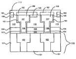
- FIG. 1Athere is shown a metallization level 100 on which a metallization level according to an embodiment of the present invention may be formed. It is to be understood, however, that metallization level 100 is being provided herein only for illustration purposes; metallization levels according to embodiments of the present invention may be employed as a first, last, or intervening metallization level.
- Metalization level 100includes metal structures 102 .
- Metal structures 102may be formed using a damascene, dual-damascene, or other metallization process.
- Metal structures 102may be made of copper or aluminum, for example.
- Dielectrics 101electrically isolate one metal structure 102 from another.
- Dielectrics 101may be of TEOS or other low-k dielectric material, for example.
- a capping layer 103is deposited overlying metallization level 100 .
- Capping layer 103separates metallization level 100 from an overlying metallization level; capping layer 103 may also function as a barrier layer for minimizing metal diffusion.
- capping layer 103may be of silicon nitride (Si 3 N 4 ) deposited to a thickness of 500 Angstroms by plasma enhanced chemical vapor deposition (PECVD).
- PECVDplasma enhanced chemical vapor deposition
- Other non-conductive materialsmay also be used instead of silicon nitride.
- silicon carbide or silicon nitride carbidemay also be used as a capping layer 103 .
- a support layer 104is deposited overlying capping layer 103 .
- Support layer 104provides structural support to a subsequently formed floating metal structure overlying metallization level 100 .
- the floating metal structureincludes a via and an interconnect line; the via is formed through support layer 104 in that embodiment.
- Support layer 104may be a silicon dioxide layer (SiO 2 ) deposited to a thickness of 3000 Angstroms by PECVD, for example.
- support layer 104is of a low-k dielectric material.
- a sacrificial layer 105is deposited overlying support layer 104 .
- Sacrificial layer 105is used to define the subsequently formed floating metal structure, and is advantageously of a material preferentially etched by a noble gas fluoride.
- sacrificial layer 105may be of a silicon material such as polycrystalline silicon or amorphous silicon. The silicon material may be etched using a noble gas fluoride such as xenon difluoride (XeF 2 ).
- a sacrificial layer 105 of polycrystalline siliconmay be deposited by PECVD or physical vapor deposition (PVD) to a thickness of 5000 Angstroms, for example.
- Non-conductive layer 106is optionally deposited overlying sacrificial layer 105 .
- Non-conductive layer 106provides additional structural support to the subsequently formed floating metal structure, and may not be needed in some applications.
- Non-conductive layer 106may be a silicon nitride layer deposited by PECVD to a thickness of 500 Angstroms, for example.
- Other non-conductive materialsmay also be used instead of silicon nitride.
- silicon dioxide or silicon carbidemay also be used as a non-conductive layer 106 .
- a dual-damascene etch processis performed on the sample of FIG. 1D to form vias 108 and interconnect line patterns 107 .
- Any type of dual-damascene etch processmay be used to form vias 108 and interconnect line patterns 107 without detracting from the merits of the present invention.
- either a “via first” or a “line first” dual-damascene etch processmay be employed to form vias 108 and interconnect line patterns 107 .
- the following exampleillustrates a line first dual-damascene etch process.
- vias 108are formed by etching through layers 106 , 105 , 104 , and 103 .
- interconnect line patterns 107are formed by etching layers 106 and 105 .
- a barrier layer 161is deposited on the sample of FIG. 1F prior to depositing a metal in interconnect line patterns 107 and vias 108 .
- a barrier layer 161 of tantalum/tantalum nitridemay be deposited by PVD.
- a metal 109is deposited in vias 108 and interconnect line patterns 107 .
- Metal 109fills vias 108 to from via connections to metallization level 100 , and fills interconnect line patterns 107 to form interconnect lines coupled to metal structures 102 .
- a metal 109 of coppermay be deposited by first depositing a copper seed layer, followed by a bulk copper electroplating step. (The seed layer is not depicted for clarity.)
- metal 109is planarized.
- a metal 109 of coppermay be planarized by chemical-mechanical polishing (CMP).
- a capping layer 162is deposited on the sample of FIG. 1I .
- Capping layer 162helps minimize copper migration and provides structural support in applications where additional levels will be formed over the subsequently formed floating metal structure.
- Capping layer 162may be a silicon nitride layer deposited to a thickness of 500 Angtroms by PECVD, for example. Other materials may also be used as a capping layer 162 including silicon carbide.
- capping layer 162 and non-conductive layer 106are etched to form windows 110 .
- Windows 110expose the underlying sacrificial layer 105 .
- native oxide on the surface of sacrificial layer 105may have to be removed.
- a sacrificial layer 105 of polycrystalline siliconmay have native oxide thereon.
- the sample of FIG. 1Kis first dipped in a pre-etch solution of ethylene glycol and ammonium fluoride prior to etching sacrificial layer 105 .
- a suitable commercially available pre-etch solutionincludes that of the type available from ACSI, Inc. of Milpitas, Calif. under the name NOE Etch ITM solution.
- the sample of FIG. 1Kis placed in an environment including a noble gas fluoride to etch sacrificial layer 105 .
- the sample of FIG. 1Kmay be placed in a vacuum chamber (not shown) where a noble gas fluoride is introduced.
- the sampleis left in the chamber for a time sufficient to etch most of the remaining sacrificial layer 105 and form air cores 112 (e.g., 2 to 5 minutes; chamber pressure of 50 ⁇ 10 ⁇ 3 Torr).
- the process parameters for etching sacrificial layer 105 using a noble gas fluoridedepend on the chamber used, the physical details of the sample, etc.
- the noble gas fluorideincludes xenon difluoride.
- Other noble gas fluorides that may be usedinclude those of krypton and argon.
- Xenon difluoridehas been used as an etchant in micro-electro-mechanical systems (MEMS) applications.
- MEMSmicro-electro-mechanical systems
- U.S. Pat. No. 5,726,480 issued to Pisterdiscloses the use of xenon difluoride in the fabrication of MEMS structures.
- U.S. application Ser. No. 09/952,626, entitled “MICROELECTRONIC MECHANICAL SYSTEM AND METHODS”, filed by Mike Bruner on Sep. 13, 2001also discloses the use of xenon difluoride as an etchant.
- the aforementioned disclosures by Pister and Brunerare incorporated herein by reference in their entirety.
- an integrated circuitemploys metals primarily to carry electrical signals. Reducing the capacitance on a metal line, while of minimal concern to the fabrication of MEMS structures, is important in integrated circuit applications.
- the step of etching sacrificial layer 105 using a noble gas fluorideresults in air cores 112 surrounding metal 109 .
- Each metal 109is now a “floating” metal structure in that an air-filled space (i.e., an air core 112 ) surrounds it.
- An air core 112is a unity-k dielectric region because air has a dielectric constant approximately equal to 1.
- air cores 112lower the capacitance on metals 109 and help increase signal propagation speeds.
- a method of forming a floating metal structure in accordance with an embodiment of the present inventionallows for the creation of a unity-k dielectric region without having to employ complex structural systems.
- topside layer 113is deposited on the sample of FIG. 1L .
- Topside layer 113provides a base on which overlying metallization levels may be formed.
- Topside layer 113may be a silicon nitride layer deposited by PECVD to a thickness of 500 Angstroms if it is a middle layer or 9000 Angstroms if it is the last layer, for example.
- Topside layer 113may also be of other non-conductive material including oxynitride.
- a support layeris deposited overlying a metallization level.
- the support layerwhich may be of silicon dioxide, provides structural support to a subsequently formed floating metal structure.
- a sacrificial layeris deposited overlying the support layer.
- the sacrificial layerdefines the subsequently formed floating metal structure.
- the sacrificial layermay be a silicon material such as polycrystalline silicon or amorphous silicon.
- a non-conductive layersuch as silicon nitride is deposited overlying the sacrificial layer to provide additional structural support to the floating metal structure.
- a via and an interconnect line patternare formed in the sacrificial layer.
- the via and the interconnect line patternmay be formed using a dual-damascene etch process.
- step 208a metal is deposited in the via and the interconnect line pattern. This results in an interconnect line coupled to a metal line in a lower metallization level.
- step 210the metal is planarized.
- a capping layeris deposited overlying the metal.
- the capping layerhelps minimize copper migration and provides structural support in applications where additional levels will be formed over the subsequently formed floating metal structure.
- a windowis formed at least through the capping layer (and any other layers between the capping layer and the sacrificial layer) to expose the sacrificial layer.
- Native oxide on the exposed surface of the sacrificial layermay have to be removed prior to the subsequent etching of the sacrificial layer.
- the sacrificial layeris etched using a chemistry that includes a noble gas fluoride.
- a sacrificial layer of polycrystalline siliconmay be etched using a chemistry that includes xenon difluoride. This etching step “floats” the metal by creating an air core surrounding the metal. The air core provides a unity-k dielectric region that lowers the resulting capacitance on the metal.
Landscapes
- Engineering & Computer Science (AREA)
- Physics & Mathematics (AREA)
- Condensed Matter Physics & Semiconductors (AREA)
- General Physics & Mathematics (AREA)
- Computer Hardware Design (AREA)
- Microelectronics & Electronic Packaging (AREA)
- Power Engineering (AREA)
- Manufacturing & Machinery (AREA)
- Internal Circuitry In Semiconductor Integrated Circuit Devices (AREA)
Abstract
Description
Claims (16)
Priority Applications (1)
| Application Number | Priority Date | Filing Date | Title |
|---|---|---|---|
| US10/072,164US7026235B1 (en) | 2002-02-07 | 2002-02-07 | Dual-damascene process and associated floating metal structures |
Applications Claiming Priority (1)
| Application Number | Priority Date | Filing Date | Title |
|---|---|---|---|
| US10/072,164US7026235B1 (en) | 2002-02-07 | 2002-02-07 | Dual-damascene process and associated floating metal structures |
Publications (1)
| Publication Number | Publication Date |
|---|---|
| US7026235B1true US7026235B1 (en) | 2006-04-11 |
Family
ID=36127689
Family Applications (1)
| Application Number | Title | Priority Date | Filing Date |
|---|---|---|---|
| US10/072,164Expired - LifetimeUS7026235B1 (en) | 2002-02-07 | 2002-02-07 | Dual-damascene process and associated floating metal structures |
Country Status (1)
| Country | Link |
|---|---|
| US (1) | US7026235B1 (en) |
Cited By (15)
| Publication number | Priority date | Publication date | Assignee | Title |
|---|---|---|---|---|
| US20060141767A1 (en)* | 2004-12-29 | 2006-06-29 | Han Jae W | Metal wiring for semiconductor device and method for forming the same |
| US20070117396A1 (en)* | 2005-11-22 | 2007-05-24 | Dingjun Wu | Selective etching of titanium nitride with xenon difluoride |
| JP2007305986A (en)* | 2006-05-08 | 2007-11-22 | Internatl Business Mach Corp <Ibm> | Method of forming multilayer interconnect structure including interconnected conductive wiring and vias spaced apart by combination of solid and gaseous dielectric, and multilevel interconnect structure containing air-gaps (multilayer interconnect structure containing air gaps and method of fabricating the same) |
| US20100022095A1 (en)* | 2005-11-22 | 2010-01-28 | Air Products And Chemicals, Inc. | Selective Etching and Formation of Xenon Difluoride |
| US20100164059A1 (en)* | 2008-12-25 | 2010-07-01 | Fujitsu Limited | Semiconductor device and manufacturing method thereof |
| US20100301489A1 (en)* | 2009-05-29 | 2010-12-02 | Robert Seidel | Microstructure device including a metallization structure with self-aligned air gaps formed based on a sacrificial material |
| US20110171823A1 (en)* | 2006-05-04 | 2011-07-14 | Hussein Makarem A | Dielectric spacers for metal interconnects and method to form the same |
| US8592891B1 (en) | 2007-05-25 | 2013-11-26 | Cypress Semiconductor Corp. | Methods for fabricating semiconductor memory with process induced strain |
| US8691648B1 (en) | 2007-05-25 | 2014-04-08 | Cypress Semiconductor Corporation | Methods for fabricating semiconductor memory with process induced strain |
| US20150262860A1 (en)* | 2014-03-14 | 2015-09-17 | Taiwan Semiconductor Manufacturing Company, Ltd. | Method of Semiconductor Integrated Circuit Fabrication |
| US9443956B2 (en) | 2014-12-08 | 2016-09-13 | Globalfoundries Inc. | Method for forming air gap structure using carbon-containing spacer |
| US9583380B2 (en) | 2014-07-17 | 2017-02-28 | Globalfoundries Inc. | Anisotropic material damage process for etching low-K dielectric materials |
| US9768058B2 (en) | 2015-08-10 | 2017-09-19 | Globalfoundries Inc. | Methods of forming air gaps in metallization layers on integrated circuit products |
| US10229873B2 (en) | 2017-02-07 | 2019-03-12 | International Business Machines Corporation | Three plate MIM capacitor via integrity verification |
| US11527477B2 (en)* | 2020-03-16 | 2022-12-13 | Kioxia Corporation | Semiconductor device and method of manufacturing semiconductor device |
Citations (39)
| Publication number | Priority date | Publication date | Assignee | Title |
|---|---|---|---|---|
| US4190488A (en) | 1978-08-21 | 1980-02-26 | International Business Machines Corporation | Etching method using noble gas halides |
| US4498953A (en) | 1983-07-27 | 1985-02-12 | At&T Bell Laboratories | Etching techniques |
| US4749440A (en) | 1985-08-28 | 1988-06-07 | Fsi Corporation | Gaseous process and apparatus for removing films from substrates |
| US4789648A (en) | 1985-10-28 | 1988-12-06 | International Business Machines Corporation | Method for producing coplanar multi-level metal/insulator films on a substrate and for forming patterned conductive lines simultaneously with stud vias |
| US4944836A (en) | 1985-10-28 | 1990-07-31 | International Business Machines Corporation | Chem-mech polishing method for producing coplanar metal/insulator films on a substrate |
| US4956313A (en) | 1987-08-17 | 1990-09-11 | International Business Machines Corporation | Via-filling and planarization technique |
| US5030319A (en) | 1988-12-27 | 1991-07-09 | Kabushiki Kaisha Toshiba | Method of oxide etching with condensed plasma reaction product |
| US5262354A (en) | 1992-02-26 | 1993-11-16 | International Business Machines Corporation | Refractory metal capped low resistivity metal conductor lines and vias |
| US5312777A (en) | 1992-09-25 | 1994-05-17 | International Business Machines Corporation | Fabrication methods for bidirectional field emission devices and storage structures |
| US5354416A (en) | 1986-09-05 | 1994-10-11 | Sadayuki Okudaira | Dry etching method |
| US5397741A (en) | 1993-03-29 | 1995-03-14 | International Business Machines Corporation | Process for metallized vias in polyimide |
| US5453639A (en) | 1992-09-04 | 1995-09-26 | International Business Machines Corporation | Planarized semiconductor structure using subminimum features |
| US5534107A (en) | 1994-06-14 | 1996-07-09 | Fsi International | UV-enhanced dry stripping of silicon nitride films |
| US5668398A (en) | 1994-05-27 | 1997-09-16 | Texas Instruments Incorporated | Multilevel interconnect structure with air gaps formed between metal leads |
| US5676587A (en) | 1995-12-06 | 1997-10-14 | International Business Machines Corporation | Selective polish process for titanium, titanium nitride, tantalum and tantalum nitride |
| US5716495A (en) | 1994-06-14 | 1998-02-10 | Fsi International | Cleaning method |
| US5726480A (en) | 1995-01-27 | 1998-03-10 | The Regents Of The University Of California | Etchants for use in micromachining of CMOS Microaccelerometers and microelectromechanical devices and method of making the same |
| US5918149A (en) | 1996-02-16 | 1999-06-29 | Advanced Micro Devices, Inc. | Deposition of a conductor in a via hole or trench |
| US5963830A (en) | 1996-08-02 | 1999-10-05 | Mosel Vitelic Incorporated | Method of forming a TiN/W barrier layer for a hot Al plug |
| US6015599A (en) | 1994-03-07 | 2000-01-18 | Regents Of The University Of California | High vertical aspect ratio thin film structures |
| US6117748A (en) | 1998-04-15 | 2000-09-12 | Worldwide Semiconductor Manufacturing Corporation | Dishing free process for shallow trench isolation |
| US6120844A (en) | 1995-11-21 | 2000-09-19 | Applied Materials, Inc. | Deposition film orientation and reflectivity improvement using a self-aligning ultra-thin layer |
| US6197610B1 (en) | 2000-01-14 | 2001-03-06 | Ball Semiconductor, Inc. | Method of making small gaps for small electrical/mechanical devices |
| US6204200B1 (en) | 1997-05-05 | 2001-03-20 | Texas Instruments Incorporated | Process scheme to form controlled airgaps between interconnect lines to reduce capacitance |
| US6254792B1 (en) | 1997-11-10 | 2001-07-03 | Advanced Technology Materials, Inc. | Isotropic dry cleaning process for noble metal integrated circuit structures |
| US6271145B1 (en) | 1999-05-31 | 2001-08-07 | Ball Semiconductor, Inc. | Method for making a micromachine |
| US6290864B1 (en) | 1999-10-26 | 2001-09-18 | Reflectivity, Inc. | Fluoride gas etching of silicon with improved selectivity |
| US6331459B1 (en) | 1999-02-18 | 2001-12-18 | Infineon Technologies Ag | Use of dummy poly spacers and divot fill techniques for DT-aligned processing after STI formation for advanced deep trench capacitor DRAM |
| US6355498B1 (en)* | 2000-08-11 | 2002-03-12 | Agere Systems Guartian Corp. | Thin film resonators fabricated on membranes created by front side releasing |
| US6372632B1 (en) | 2000-01-24 | 2002-04-16 | Taiwan Semiconductor Manufacturing Company | Method to eliminate dishing of copper interconnects by the use of a sacrificial oxide layer |
| US6413852B1 (en)* | 2000-08-31 | 2002-07-02 | International Business Machines Corporation | Method of forming multilevel interconnect structure containing air gaps including utilizing both sacrificial and placeholder material |
| US6436787B1 (en) | 2001-07-26 | 2002-08-20 | Taiwan Semiconductor Manufacturing Company | Method of forming crown-type MIM capacitor integrated with the CU damascene process |
| US6461888B1 (en) | 2001-06-14 | 2002-10-08 | Institute Of Microelectronics | Lateral polysilicon beam process |
| US6496348B2 (en) | 1998-03-10 | 2002-12-17 | Mcintosh Robert B. | Method to force-balance capacitive transducers |
| US20030036215A1 (en) | 2001-07-20 | 2003-02-20 | Reflectivity, Inc., A Delaware Corporation | MEMS device made of transition metal-dielectric oxide materials |
| US6531331B1 (en) | 2002-07-16 | 2003-03-11 | Sandia Corporation | Monolithic integration of a MOSFET with a MEMS device |
| US20030054588A1 (en) | 2000-12-07 | 2003-03-20 | Reflectivity, Inc., A California Corporation | Methods for depositing, releasing and packaging micro-electromechanical devices on wafer substrates |
| US20030073302A1 (en)* | 2001-10-12 | 2003-04-17 | Reflectivity, Inc., A California Corporation | Methods for formation of air gap interconnects |
| US6555467B2 (en)* | 2001-09-28 | 2003-04-29 | Sharp Laboratories Of America, Inc. | Method of making air gaps copper interconnect |
- 2002
- 2002-02-07USUS10/072,164patent/US7026235B1/ennot_activeExpired - Lifetime
Patent Citations (39)
| Publication number | Priority date | Publication date | Assignee | Title |
|---|---|---|---|---|
| US4190488A (en) | 1978-08-21 | 1980-02-26 | International Business Machines Corporation | Etching method using noble gas halides |
| US4498953A (en) | 1983-07-27 | 1985-02-12 | At&T Bell Laboratories | Etching techniques |
| US4749440A (en) | 1985-08-28 | 1988-06-07 | Fsi Corporation | Gaseous process and apparatus for removing films from substrates |
| US4789648A (en) | 1985-10-28 | 1988-12-06 | International Business Machines Corporation | Method for producing coplanar multi-level metal/insulator films on a substrate and for forming patterned conductive lines simultaneously with stud vias |
| US4944836A (en) | 1985-10-28 | 1990-07-31 | International Business Machines Corporation | Chem-mech polishing method for producing coplanar metal/insulator films on a substrate |
| US5354416A (en) | 1986-09-05 | 1994-10-11 | Sadayuki Okudaira | Dry etching method |
| US4956313A (en) | 1987-08-17 | 1990-09-11 | International Business Machines Corporation | Via-filling and planarization technique |
| US5030319A (en) | 1988-12-27 | 1991-07-09 | Kabushiki Kaisha Toshiba | Method of oxide etching with condensed plasma reaction product |
| US5262354A (en) | 1992-02-26 | 1993-11-16 | International Business Machines Corporation | Refractory metal capped low resistivity metal conductor lines and vias |
| US5453639A (en) | 1992-09-04 | 1995-09-26 | International Business Machines Corporation | Planarized semiconductor structure using subminimum features |
| US5312777A (en) | 1992-09-25 | 1994-05-17 | International Business Machines Corporation | Fabrication methods for bidirectional field emission devices and storage structures |
| US5397741A (en) | 1993-03-29 | 1995-03-14 | International Business Machines Corporation | Process for metallized vias in polyimide |
| US6015599A (en) | 1994-03-07 | 2000-01-18 | Regents Of The University Of California | High vertical aspect ratio thin film structures |
| US5668398A (en) | 1994-05-27 | 1997-09-16 | Texas Instruments Incorporated | Multilevel interconnect structure with air gaps formed between metal leads |
| US5534107A (en) | 1994-06-14 | 1996-07-09 | Fsi International | UV-enhanced dry stripping of silicon nitride films |
| US5716495A (en) | 1994-06-14 | 1998-02-10 | Fsi International | Cleaning method |
| US5726480A (en) | 1995-01-27 | 1998-03-10 | The Regents Of The University Of California | Etchants for use in micromachining of CMOS Microaccelerometers and microelectromechanical devices and method of making the same |
| US6120844A (en) | 1995-11-21 | 2000-09-19 | Applied Materials, Inc. | Deposition film orientation and reflectivity improvement using a self-aligning ultra-thin layer |
| US5676587A (en) | 1995-12-06 | 1997-10-14 | International Business Machines Corporation | Selective polish process for titanium, titanium nitride, tantalum and tantalum nitride |
| US5918149A (en) | 1996-02-16 | 1999-06-29 | Advanced Micro Devices, Inc. | Deposition of a conductor in a via hole or trench |
| US5963830A (en) | 1996-08-02 | 1999-10-05 | Mosel Vitelic Incorporated | Method of forming a TiN/W barrier layer for a hot Al plug |
| US6204200B1 (en) | 1997-05-05 | 2001-03-20 | Texas Instruments Incorporated | Process scheme to form controlled airgaps between interconnect lines to reduce capacitance |
| US6254792B1 (en) | 1997-11-10 | 2001-07-03 | Advanced Technology Materials, Inc. | Isotropic dry cleaning process for noble metal integrated circuit structures |
| US6496348B2 (en) | 1998-03-10 | 2002-12-17 | Mcintosh Robert B. | Method to force-balance capacitive transducers |
| US6117748A (en) | 1998-04-15 | 2000-09-12 | Worldwide Semiconductor Manufacturing Corporation | Dishing free process for shallow trench isolation |
| US6331459B1 (en) | 1999-02-18 | 2001-12-18 | Infineon Technologies Ag | Use of dummy poly spacers and divot fill techniques for DT-aligned processing after STI formation for advanced deep trench capacitor DRAM |
| US6271145B1 (en) | 1999-05-31 | 2001-08-07 | Ball Semiconductor, Inc. | Method for making a micromachine |
| US6290864B1 (en) | 1999-10-26 | 2001-09-18 | Reflectivity, Inc. | Fluoride gas etching of silicon with improved selectivity |
| US6197610B1 (en) | 2000-01-14 | 2001-03-06 | Ball Semiconductor, Inc. | Method of making small gaps for small electrical/mechanical devices |
| US6372632B1 (en) | 2000-01-24 | 2002-04-16 | Taiwan Semiconductor Manufacturing Company | Method to eliminate dishing of copper interconnects by the use of a sacrificial oxide layer |
| US6355498B1 (en)* | 2000-08-11 | 2002-03-12 | Agere Systems Guartian Corp. | Thin film resonators fabricated on membranes created by front side releasing |
| US6413852B1 (en)* | 2000-08-31 | 2002-07-02 | International Business Machines Corporation | Method of forming multilevel interconnect structure containing air gaps including utilizing both sacrificial and placeholder material |
| US20030054588A1 (en) | 2000-12-07 | 2003-03-20 | Reflectivity, Inc., A California Corporation | Methods for depositing, releasing and packaging micro-electromechanical devices on wafer substrates |
| US6461888B1 (en) | 2001-06-14 | 2002-10-08 | Institute Of Microelectronics | Lateral polysilicon beam process |
| US20030036215A1 (en) | 2001-07-20 | 2003-02-20 | Reflectivity, Inc., A Delaware Corporation | MEMS device made of transition metal-dielectric oxide materials |
| US6436787B1 (en) | 2001-07-26 | 2002-08-20 | Taiwan Semiconductor Manufacturing Company | Method of forming crown-type MIM capacitor integrated with the CU damascene process |
| US6555467B2 (en)* | 2001-09-28 | 2003-04-29 | Sharp Laboratories Of America, Inc. | Method of making air gaps copper interconnect |
| US20030073302A1 (en)* | 2001-10-12 | 2003-04-17 | Reflectivity, Inc., A California Corporation | Methods for formation of air gap interconnects |
| US6531331B1 (en) | 2002-07-16 | 2003-03-11 | Sandia Corporation | Monolithic integration of a MOSFET with a MEMS device |
Non-Patent Citations (9)
| Title |
|---|
| Chung-Hui Chen, Yean-Kuen Fang, Chih-Wei Yang, and C.S. Tang, A Deep Submicron CMOS Process Compatible Susupending High-Q Inductor, IEEE Electron Device Letters, Nov. 11, 2001, pp. 522-523, vol. 22, No. 11, Taiwan R.O.C. |
| D.E. Ibbotson, J.A. Mucha, and D.L. Flamm, J.M. Cook,Plasmaless dry etching of silicon with fluorine-containing compounds, J. Appl. Phys., Nov. 15, 1984, pp. 2939-2942, vol. 56, No. 10, AT&T Bell Laboratories, Murray Hill, New Jersey, and Allentown, Pennsylvania, USA. |
| Dale E. Ibbotson, Daniel L. Flamm, John A. Mucha, and Vincent M. Donnelly, Comparison of XeF2 and F-atom reactions with Si and SiO2, Appl. Phys. Lett. Jun. 15, 1984, pp. 1129-1131, vol. 44, No. 12, AT&T Bell Laboratories, Murray Hill, New Jersey, USA. |
| F.A. Houle, Dynamics of SiF4 desorption during etching of silicon by XeF2, J. Chem. Phys. Aug. 1987, pp. 1866-1872, vol. 87, No. 3, IBM Research Center, San Jose, California, USA. |
| H.F. Winters and J. W. Coburn, The etching of silicon with XeF2 vapor, Appl. Phys. Lett. Jan. 1979, pp. 70-73, vol. 34, No. 1, IBM Research Lab, San Jose, California, USA. |
| Karl Bohringer, EE 539 Autumm 1999, Slide 1-14 [retrieved on Nov. 20, 2001]. Retrieved from the internet: <URL:http//www.ee.washington.edu/class/539/Lectures/lecture3/sld001-014.html>. |
| Seong Geon Park, et al. "A New ALD-TiN/CoSi2 Contact Plug Process for Reliable and Low Defect Density Bit-Line Integration in Sub-Quarter Micron Giga-bit DRAM" pp. 282-284, Semiconductor R&D Center, Samsung Electronics Co. LTD., Korea. |
| Thomas E. Wade, Gas Dome System , Provides Unity-K Dielectric, Semiconductor International, pp. 125, 126,128, 130, and 133, University of South Florida, Tampa, Florida, USA. |
| V.S. Aliev and V.N. Kruchinin, Development of Si (100) surface roughness at the intial stage of etching in F2 and XeF2 gases: ellipsometric study, Surface Science 442 (1999) pp. 206-214, Elsevier Science, Novosibirsk, Russia. |
Cited By (23)
| Publication number | Priority date | Publication date | Assignee | Title |
|---|---|---|---|---|
| US7397122B2 (en)* | 2004-12-29 | 2008-07-08 | Dongbu Electronics Co., Ltd. | Metal wiring for semiconductor device and method for forming the same |
| US20060141767A1 (en)* | 2004-12-29 | 2006-06-29 | Han Jae W | Metal wiring for semiconductor device and method for forming the same |
| US8278222B2 (en) | 2005-11-22 | 2012-10-02 | Air Products And Chemicals, Inc. | Selective etching and formation of xenon difluoride |
| US20070117396A1 (en)* | 2005-11-22 | 2007-05-24 | Dingjun Wu | Selective etching of titanium nitride with xenon difluoride |
| US20100022095A1 (en)* | 2005-11-22 | 2010-01-28 | Air Products And Chemicals, Inc. | Selective Etching and Formation of Xenon Difluoride |
| US20110171823A1 (en)* | 2006-05-04 | 2011-07-14 | Hussein Makarem A | Dielectric spacers for metal interconnects and method to form the same |
| JP2007305986A (en)* | 2006-05-08 | 2007-11-22 | Internatl Business Mach Corp <Ibm> | Method of forming multilayer interconnect structure including interconnected conductive wiring and vias spaced apart by combination of solid and gaseous dielectric, and multilevel interconnect structure containing air-gaps (multilayer interconnect structure containing air gaps and method of fabricating the same) |
| US8691648B1 (en) | 2007-05-25 | 2014-04-08 | Cypress Semiconductor Corporation | Methods for fabricating semiconductor memory with process induced strain |
| US8592891B1 (en) | 2007-05-25 | 2013-11-26 | Cypress Semiconductor Corp. | Methods for fabricating semiconductor memory with process induced strain |
| US20100164059A1 (en)* | 2008-12-25 | 2010-07-01 | Fujitsu Limited | Semiconductor device and manufacturing method thereof |
| US8786086B2 (en)* | 2008-12-25 | 2014-07-22 | Fujitsu Limited | Semiconductor device including wiring having main portion and extended portion |
| DE102009023377B4 (en)* | 2009-05-29 | 2017-12-28 | Globalfoundries Dresden Module One Limited Liability Company & Co. Kg | Method for producing a microstructure component having a metallization structure with self-aligned air gap |
| US20100301489A1 (en)* | 2009-05-29 | 2010-12-02 | Robert Seidel | Microstructure device including a metallization structure with self-aligned air gaps formed based on a sacrificial material |
| DE102009023377A1 (en)* | 2009-05-29 | 2010-12-16 | Globalfoundries Dresden Module One Limited Liability Company & Co. Kg | A microstructure device having a self-aligned air gap metallization structure made on the basis of a sacrificial material |
| US8048796B2 (en) | 2009-05-29 | 2011-11-01 | Globalfoundries Inc. | Microstructure device including a metallization structure with self-aligned air gaps formed based on a sacrificial material |
| US20150262860A1 (en)* | 2014-03-14 | 2015-09-17 | Taiwan Semiconductor Manufacturing Company, Ltd. | Method of Semiconductor Integrated Circuit Fabrication |
| US9455178B2 (en)* | 2014-03-14 | 2016-09-27 | Taiwan Semiconductor Manufacturing Company, Ltd. | Method of semiconductor integrated circuit fabrication |
| US9583380B2 (en) | 2014-07-17 | 2017-02-28 | Globalfoundries Inc. | Anisotropic material damage process for etching low-K dielectric materials |
| US9443956B2 (en) | 2014-12-08 | 2016-09-13 | Globalfoundries Inc. | Method for forming air gap structure using carbon-containing spacer |
| US9768058B2 (en) | 2015-08-10 | 2017-09-19 | Globalfoundries Inc. | Methods of forming air gaps in metallization layers on integrated circuit products |
| US10229873B2 (en) | 2017-02-07 | 2019-03-12 | International Business Machines Corporation | Three plate MIM capacitor via integrity verification |
| US10262934B2 (en) | 2017-02-07 | 2019-04-16 | International Business Machines Corporation | Three plate MIM capacitor via integrity verification |
| US11527477B2 (en)* | 2020-03-16 | 2022-12-13 | Kioxia Corporation | Semiconductor device and method of manufacturing semiconductor device |
Similar Documents
| Publication | Publication Date | Title |
|---|---|---|
| US7026235B1 (en) | Dual-damascene process and associated floating metal structures | |
| JP5255292B2 (en) | Interconnect structure having two-layer metal cap and method of manufacturing the same | |
| US7560375B2 (en) | Gas dielectric structure forming methods | |
| US6177329B1 (en) | Integrated circuit structures having gas pockets and method for forming integrated circuit structures having gas pockets | |
| JP5430946B2 (en) | Interconnect structure forming method | |
| US5891804A (en) | Process for conductors with selective deposition | |
| US8822331B2 (en) | Anchored damascene structures | |
| TWI442512B (en) | An interconnect structure with dielectric air gaps | |
| US6331481B1 (en) | Damascene etchback for low ε dielectric | |
| EP1521301A1 (en) | Method of formation of airgaps around interconnecting line | |
| US20040232552A1 (en) | Air gap dual damascene process and structure | |
| US20020142581A1 (en) | Interconnection structure and method for fabricating same | |
| US6413854B1 (en) | Method to build multi level structure | |
| US6686273B2 (en) | Method of fabricating copper interconnects with very low-k inter-level insulator | |
| US6339029B1 (en) | Method to form copper interconnects | |
| US6406992B1 (en) | Fabrication method for a dual damascene structure | |
| US6313025B1 (en) | Process for manufacturing an integrated circuit including a dual-damascene structure and an integrated circuit | |
| US7169701B2 (en) | Dual damascene trench formation to avoid low-K dielectric damage | |
| US6365327B1 (en) | Process for manufacturing in integrated circuit including a dual-damascene structure and an integrated circuit | |
| US6835616B1 (en) | Method of forming a floating metal structure in an integrated circuit | |
| US6204096B1 (en) | Method for reducing critical dimension of dual damascene process using spin-on-glass process | |
| US6352919B1 (en) | Method of fabricating a borderless via | |
| KR20040101008A (en) | Manufacturing method for semiconductor apparatus | |
| KR100688758B1 (en) | Method for forming gap fill for metal wiring in semiconductor device | |
| JP2003124312A (en) | Semiconductor device and method of manufacturing the same |
Legal Events
| Date | Code | Title | Description |
|---|---|---|---|
| AS | Assignment | Owner name:CYPRESS SEMICONDUCTOR CORPORATION, CALIFORNIA Free format text:ASSIGNMENT OF ASSIGNORS INTEREST;ASSIGNORS:BEN-TZUR, MIRA;RAMKUMAR, KRISHNASWAMY;REEL/FRAME:012577/0165 Effective date:20020204 | |
| STCF | Information on status: patent grant | Free format text:PATENTED CASE | |
| FEPP | Fee payment procedure | Free format text:PAYOR NUMBER ASSIGNED (ORIGINAL EVENT CODE: ASPN); ENTITY STATUS OF PATENT OWNER: LARGE ENTITY | |
| REMI | Maintenance fee reminder mailed | ||
| FPAY | Fee payment | Year of fee payment:4 | |
| SULP | Surcharge for late payment | ||
| FPAY | Fee payment | Year of fee payment:8 | |
| AS | Assignment | Owner name:MORGAN STANLEY SENIOR FUNDING, INC., NEW YORK Free format text:SECURITY INTEREST;ASSIGNORS:CYPRESS SEMICONDUCTOR CORPORATION;SPANSION LLC;REEL/FRAME:035240/0429 Effective date:20150312 | |
| MAFP | Maintenance fee payment | Free format text:PAYMENT OF MAINTENANCE FEE, 12TH YEAR, LARGE ENTITY (ORIGINAL EVENT CODE: M1553) Year of fee payment:12 | |
| AS | Assignment | Owner name:MUFG UNION BANK, N.A., CALIFORNIA Free format text:ASSIGNMENT AND ASSUMPTION OF SECURITY INTEREST IN INTELLECTUAL PROPERTY;ASSIGNOR:MORGAN STANLEY SENIOR FUNDING, INC.;REEL/FRAME:050896/0366 Effective date:20190731 | |
| AS | Assignment | Owner name:MORGAN STANLEY SENIOR FUNDING, INC., NEW YORK Free format text:CORRECTIVE ASSIGNMENT TO CORRECT THE 8647899 PREVIOUSLY RECORDED ON REEL 035240 FRAME 0429. ASSIGNOR(S) HEREBY CONFIRMS THE SECURITY INTERST;ASSIGNORS:CYPRESS SEMICONDUCTOR CORPORATION;SPANSION LLC;REEL/FRAME:058002/0470 Effective date:20150312 | |
| AS | Assignment | Owner name:SPANSION LLC, CALIFORNIA Free format text:RELEASE BY SECURED PARTY;ASSIGNOR:MUFG UNION BANK, N.A.;REEL/FRAME:059410/0438 Effective date:20200416 Owner name:CYPRESS SEMICONDUCTOR CORPORATION, CALIFORNIA Free format text:RELEASE BY SECURED PARTY;ASSIGNOR:MUFG UNION BANK, N.A.;REEL/FRAME:059410/0438 Effective date:20200416 | |
| AS | Assignment | Owner name:INFINEON TECHNOLOGIES LLC, CALIFORNIA Free format text:ASSIGNMENT OF ASSIGNORS INTEREST;ASSIGNOR:CYPRESS SEMICONDUCTOR CORPORATION;REEL/FRAME:059721/0467 Effective date:20200315 |