US7026226B1 - Method of hydrogenating a poly-silicon layer - Google Patents
Method of hydrogenating a poly-silicon layerDownload PDFInfo
- Publication number
- US7026226B1 US7026226B1US10/978,380US97838004AUS7026226B1US 7026226 B1US7026226 B1US 7026226B1US 97838004 AUS97838004 AUS 97838004AUS 7026226 B1US7026226 B1US 7026226B1
- Authority
- US
- United States
- Prior art keywords
- hydrogen
- poly
- plasma
- silicon layer
- silicon
- Prior art date
- Legal status (The legal status is an assumption and is not a legal conclusion. Google has not performed a legal analysis and makes no representation as to the accuracy of the status listed.)
- Expired - Fee Related
Links
- 238000000034methodMethods0.000titleclaimsabstractdescription43
- 229910021420polycrystalline siliconInorganic materials0.000titleclaimsabstractdescription40
- 239000001257hydrogenSubstances0.000claimsabstractdescription37
- 229910052739hydrogenInorganic materials0.000claimsabstractdescription37
- UFHFLCQGNIYNRP-UHFFFAOYSA-NHydrogenChemical compound[H][H]UFHFLCQGNIYNRP-UHFFFAOYSA-N0.000claimsabstractdescription35
- 239000002210silicon-based materialSubstances0.000claimsabstractdescription15
- 239000010409thin filmSubstances0.000claimsabstractdescription8
- 238000000623plasma-assisted chemical vapour depositionMethods0.000claimsdescription14
- 239000000758substrateSubstances0.000claimsdescription9
- 238000000151depositionMethods0.000claimsdescription7
- 239000007789gasSubstances0.000claimsdescription7
- 238000000427thin-film depositionMethods0.000claimsdescription7
- QGZKDVFQNNGYKY-UHFFFAOYSA-NAmmoniaChemical compoundNQGZKDVFQNNGYKY-UHFFFAOYSA-N0.000claimsdescription6
- 229910052581Si3N4Inorganic materials0.000claimsdescription3
- 229910004205SiNXInorganic materials0.000claimsdescription3
- HQVNEWCFYHHQES-UHFFFAOYSA-Nsilicon nitrideChemical compoundN12[Si]34N5[Si]62N3[Si]51N64HQVNEWCFYHHQES-UHFFFAOYSA-N0.000claimsdescription3
- 150000002431hydrogenChemical class0.000claimsdescription2
- 238000005229chemical vapour depositionMethods0.000claims3
- 230000015572biosynthetic processEffects0.000claims1
- 238000005984hydrogenation reactionMethods0.000abstractdescription14
- 125000004435hydrogen atomChemical group[H]*0.000abstractdescription6
- 238000004519manufacturing processMethods0.000description11
- 238000005516engineering processMethods0.000description7
- 238000007669thermal treatmentMethods0.000description7
- 229910021417amorphous siliconInorganic materials0.000description3
- 229910000069nitrogen hydrideInorganic materials0.000description3
- 239000007787solidSubstances0.000description3
- BLRPTPMANUNPDV-UHFFFAOYSA-NSilaneChemical compound[SiH4]BLRPTPMANUNPDV-UHFFFAOYSA-N0.000description2
- VYPSYNLAJGMNEJ-UHFFFAOYSA-NSilicium dioxideChemical compoundO=[Si]=OVYPSYNLAJGMNEJ-UHFFFAOYSA-N0.000description2
- 238000000137annealingMethods0.000description2
- 230000008021depositionEffects0.000description2
- 238000005268plasma chemical vapour depositionMethods0.000description2
- 229910052814silicon oxideInorganic materials0.000description2
- 101001074571Homo sapiens PIN2/TERF1-interacting telomerase inhibitor 1Proteins0.000description1
- 102100036257PIN2/TERF1-interacting telomerase inhibitor 1Human genes0.000description1
- 229910021529ammoniaInorganic materials0.000description1
- 239000000969carrierSubstances0.000description1
- 238000006243chemical reactionMethods0.000description1
- 230000007547defectEffects0.000description1
- 238000010438heat treatmentMethods0.000description1
- 238000012986modificationMethods0.000description1
- 230000004048modificationEffects0.000description1
- 238000009832plasma treatmentMethods0.000description1
- 238000004381surface treatmentMethods0.000description1
Images

Classifications
- H—ELECTRICITY
- H01—ELECTRIC ELEMENTS
- H01L—SEMICONDUCTOR DEVICES NOT COVERED BY CLASS H10
- H01L21/00—Processes or apparatus adapted for the manufacture or treatment of semiconductor or solid state devices or of parts thereof
- H01L21/02—Manufacture or treatment of semiconductor devices or of parts thereof
- H01L21/04—Manufacture or treatment of semiconductor devices or of parts thereof the devices having potential barriers, e.g. a PN junction, depletion layer or carrier concentration layer
- H01L21/18—Manufacture or treatment of semiconductor devices or of parts thereof the devices having potential barriers, e.g. a PN junction, depletion layer or carrier concentration layer the devices having semiconductor bodies comprising elements of Group IV of the Periodic Table or AIIIBV compounds with or without impurities, e.g. doping materials
- H01L21/30—Treatment of semiconductor bodies using processes or apparatus not provided for in groups H01L21/20 - H01L21/26
- H01L21/3003—Hydrogenation or deuterisation, e.g. using atomic hydrogen from a plasma
- H—ELECTRICITY
- H10—SEMICONDUCTOR DEVICES; ELECTRIC SOLID-STATE DEVICES NOT OTHERWISE PROVIDED FOR
- H10D—INORGANIC ELECTRIC SEMICONDUCTOR DEVICES
- H10D30/00—Field-effect transistors [FET]
- H10D30/01—Manufacture or treatment
- H10D30/021—Manufacture or treatment of FETs having insulated gates [IGFET]
- H10D30/031—Manufacture or treatment of FETs having insulated gates [IGFET] of thin-film transistors [TFT]
- H10D30/0321—Manufacture or treatment of FETs having insulated gates [IGFET] of thin-film transistors [TFT] comprising silicon, e.g. amorphous silicon or polysilicon
Definitions
- the present inventionrelates to a method of improving characteristics of a thin film transistor (TFT), and particularly to a method of hydrogenating a poly-silicon layer.
- TFTthin film transistor
- LTPSLow temperature poly-silicon
- TFTthin film transistor
- the LTPS displayhas a main difference in manufacturing: the LTPS display must have an anneal process where an a-Si thin film is transformed into a poly-silicon layer. With the annealing process, the mobility of carriers of the TFT may be increased up to 200 times. Further, the TFT has the advantages of high response speed, high luminance and high resolution. Therefore, the LPTS technology is considered as an indispensable technology for manufacturing the new-generation TFT display.
- the manufacturing of the LTPS TFT displaydoes not have a satisfactory yield, which is limited by the poor stability of the annealing process with a laser. Since the stability of the energy output of the laser and the manufacturing yield are low, a hydrogenation process must be applied to the succeeding process of the LTPS TFT to improve the yield and achieve mass production of the same. However, the whole process of manufacturing the TFT display is hard to control and needs a lengthy process time. Therefore, the hydrogenation technology is a critical process in improving characteristics of the LTPS TFT display.
- the solid hydrogenation processis conducted by depositing a hydrogen-rich containing layer, such as a silicon nitride layer containing hydrogen (SiN x :H) onto the poly-silicon layer along with a thermal treatment.
- the hydrogen atomsdiffuse into the poly-silicon layer and occupy some regions that are defects in the poly-silicon layer.
- the plasma processis undertaken to processing a substrate with a hydrogen-containing plasma where the de-ionized hydrogen from the plasma diffuses into the poly-silicon layer and occupies where it needs to be filled in the poly-silicon layer.
- both of the two-hydrogenation technologiesneed a long time to complete and thus increase the manufacturing costs of the TFT display.
- the present inventionprovides a method of hydrogenating a poly-silicon layer to improve characteristics of a poly-silicon TFT, in which the poly-silicon layer is subject to a plasma pre-process and then a hydrogenation process to promote the hydrogenation efficiency of the poly-silicon layer.
- the method according to the present inventionmay be implemented together with a thin film deposition system such as a plasma enhanced chemical vapor deposition (PECVD) system.
- PECVDplasma enhanced chemical vapor deposition
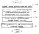
- the methodcomprises the steps of: providing a substrate with a poly-silicon layer; exciting a hydrogen-containing gas to produce a hydrogen-containing plasma; surface treating a surface of the poly-silicon layer of the substrate with the hydrogen-containing plasma; depositing a hydrogen-containing silicon-based compound on the surface of the poly-silicon layer; and thermal treating the hydrogen-containing silicon-based compound on the surface of the poly-silicon.
- FIG. 1is a flow chart of a process of an embodiment according to the present invention.
- FIG. 1is a flow chart of a process of an embodiment according to the present invention.
- the hydrogen-containing silicon-based compoundis a hydrogen-containing silicon nitride (SiN x :H).
- a plasma exciterdoes the exciting of hydrogen containing to surface treat the poly-silicon layer (step 130 ), and the hydrogen containing may be hydrogen (H 2 ) or ammonia (NH 3 ).
- the above stepsmay be executed in a same process chamber in a thin film deposition system to facilitate the entire process flow of the manufacturing of the silicon oxide product. Since the time for once of substrate load-in, substrate load-out and pre-heating is saved, the whole process may save time up to 25% as compared to the prior method of the solid hydrogenation or the plasma treatment and their accompanying successive thermal treatment.
- the hydrogen-containing plasmais excited under the conditions of a flow rate of the hydrogen-containing gas of 100 to 10000 sccm (standard cubic centimeter per minute), an input power of a radio frequency of about 100 to 5000 watts and a process chamber pressure of about 0.1 to 10 torrs.
- the thin film deposition systemmay be a plasma-enhanced chemical vapor deposition system. In this case, the deposition of the thin film may be conducted by use of a same plasma exciter. Next, using the reaction of SiH 4 and NH 3 to deposit a hydrogen-containing silicon-based compound on the surface of the poly-silicon layer.
- the conditionsare a flow rate of the SiH 4 gas of 50 to 5000 sccm, a flow rate of the NH 3 gas of about 100 to 15000 sccm, an input power of about 100 to 5000 watts and the pressure of a process chamber of about 0.1 to 10 torrs.
- a thermal treatmentis undertaken so as to make the hydrogen atoms in the hydrogen-containing silicon-based compound layer diffuse into the poly-silicon layer.
- the temperature of the thermal treatmentis higher than 400° C. and the time for the thermal treatment may be adjusted by the extent of hydrogenation as desired. The longer the thermal treatment is undertaken, the better the hydrogenating result is while the worse the real production is. However, since a plasma hydrogenation process has been previously conducted according to the present invention, the required time of thermal treatment may be shortened. Besides, the obtained hydrogenating result is better than that obtained through the prior art.
- the utilized thin film deposition systemis a plasma-enhanced chemical vapor deposition (PECVD) system and a surface treatment and the thin film deposition may be undertaken in a same process chamber by use of a same plasma exciter without any other equipment cost.
- the PECVD systemmay be selected from the group consisting of a RF-PECVD system, an electron cyclotron resonance CVD system, an ECR-CVD system, a remote plasma CVD system, a magnetic plasma CVD system and their combinations.
Landscapes
- Engineering & Computer Science (AREA)
- Physics & Mathematics (AREA)
- Plasma & Fusion (AREA)
- Condensed Matter Physics & Semiconductors (AREA)
- General Physics & Mathematics (AREA)
- Manufacturing & Machinery (AREA)
- Computer Hardware Design (AREA)
- Microelectronics & Electronic Packaging (AREA)
- Power Engineering (AREA)
Abstract
Description
Claims (13)
Priority Applications (1)
| Application Number | Priority Date | Filing Date | Title |
|---|---|---|---|
| US10/978,380US7026226B1 (en) | 2004-11-02 | 2004-11-02 | Method of hydrogenating a poly-silicon layer |
Applications Claiming Priority (1)
| Application Number | Priority Date | Filing Date | Title |
|---|---|---|---|
| US10/978,380US7026226B1 (en) | 2004-11-02 | 2004-11-02 | Method of hydrogenating a poly-silicon layer |
Publications (2)
| Publication Number | Publication Date |
|---|---|
| US7026226B1true US7026226B1 (en) | 2006-04-11 |
| US20060094211A1 US20060094211A1 (en) | 2006-05-04 |
Family
ID=36127686
Family Applications (1)
| Application Number | Title | Priority Date | Filing Date |
|---|---|---|---|
| US10/978,380Expired - Fee RelatedUS7026226B1 (en) | 2004-11-02 | 2004-11-02 | Method of hydrogenating a poly-silicon layer |
Country Status (1)
| Country | Link |
|---|---|
| US (1) | US7026226B1 (en) |
Cited By (3)
| Publication number | Priority date | Publication date | Assignee | Title |
|---|---|---|---|---|
| US8580661B1 (en)* | 2011-08-24 | 2013-11-12 | U.S. Department Of Energy | Method for the hydrogenation of poly-si |
| US20140057419A1 (en)* | 2011-11-18 | 2014-02-27 | Boe Technology Group Co., Ltd. | Method for forming low temperature polysilicon thin film |
| CN103985637A (en)* | 2014-04-30 | 2014-08-13 | 京东方科技集团股份有限公司 | Low-temperature polycrystalline silicon thin film transistor, manufacturing method thereof and display device |
Families Citing this family (1)
| Publication number | Priority date | Publication date | Assignee | Title |
|---|---|---|---|---|
| CN109065548B (en)* | 2018-07-17 | 2020-12-29 | 武汉华星光电半导体显示技术有限公司 | Array substrate and preparation method thereof |
Citations (3)
| Publication number | Priority date | Publication date | Assignee | Title |
|---|---|---|---|---|
| US5466617A (en)* | 1992-03-20 | 1995-11-14 | U.S. Philips Corporation | Manufacturing electronic devices comprising TFTs and MIMs |
| US20040229444A1 (en)* | 2003-02-18 | 2004-11-18 | Couillard James G. | Glass-based SOI structures |
| US6888200B2 (en)* | 2002-08-30 | 2005-05-03 | Micron Technology Inc. | One transistor SOI non-volatile random access memory cell |
- 2004
- 2004-11-02USUS10/978,380patent/US7026226B1/ennot_activeExpired - Fee Related
Patent Citations (3)
| Publication number | Priority date | Publication date | Assignee | Title |
|---|---|---|---|---|
| US5466617A (en)* | 1992-03-20 | 1995-11-14 | U.S. Philips Corporation | Manufacturing electronic devices comprising TFTs and MIMs |
| US6888200B2 (en)* | 2002-08-30 | 2005-05-03 | Micron Technology Inc. | One transistor SOI non-volatile random access memory cell |
| US20040229444A1 (en)* | 2003-02-18 | 2004-11-18 | Couillard James G. | Glass-based SOI structures |
Cited By (6)
| Publication number | Priority date | Publication date | Assignee | Title |
|---|---|---|---|---|
| US8580661B1 (en)* | 2011-08-24 | 2013-11-12 | U.S. Department Of Energy | Method for the hydrogenation of poly-si |
| US20140057419A1 (en)* | 2011-11-18 | 2014-02-27 | Boe Technology Group Co., Ltd. | Method for forming low temperature polysilicon thin film |
| US9633844B2 (en)* | 2011-11-18 | 2017-04-25 | Boe Technology Group Co., Ltd. | Method for forming low temperature polysilicon thin film |
| CN103985637A (en)* | 2014-04-30 | 2014-08-13 | 京东方科技集团股份有限公司 | Low-temperature polycrystalline silicon thin film transistor, manufacturing method thereof and display device |
| CN103985637B (en)* | 2014-04-30 | 2017-02-01 | 京东方科技集团股份有限公司 | Low-temperature polycrystalline silicon thin film transistor, manufacturing method thereof and display device |
| US9882057B2 (en) | 2014-04-30 | 2018-01-30 | Boe Technology Group Co., Ltd. | Low temperature poly-silicon thin film transistor and manufacturing method thereof, array substrate and display device |
Also Published As
| Publication number | Publication date |
|---|---|
| US20060094211A1 (en) | 2006-05-04 |
Similar Documents
| Publication | Publication Date | Title |
|---|---|---|
| US10699903B2 (en) | Two-step process for gapfilling high aspect ratio trenches with amorphous silicon film | |
| KR102663011B1 (en) | Methods for forming a silicon nitride film on a substrate and related semiconductor device structures | |
| US6926932B2 (en) | Method for forming silicon oxide layer | |
| US8415259B2 (en) | Method of depositing dielectric film by modified PEALD method | |
| US8173554B2 (en) | Method of depositing dielectric film having Si-N bonds by modified peald method | |
| KR20140002616A (en) | Methods for Forming a Hydrogen-Free Silicon-Containing Dielectric Film | |
| US20140273530A1 (en) | Post-Deposition Treatment Methods For Silicon Nitride | |
| US20050014365A1 (en) | Methods of forming cobalt layers for semiconductor devices | |
| TWI879747B (en) | Methods for depositing silicon nitride | |
| CN102460679A (en) | Boron film interface engineering | |
| TW201021131A (en) | Capping layers for metal oxynitride TFTs | |
| CN103843118A (en) | Insensitive dry removal process for semiconductor integration | |
| WO2009129391A2 (en) | Low temperature thin film transistor process, device property, and device stability improvement | |
| US8426288B2 (en) | Method for improving capacitance uniformity in a MIM device | |
| US20090155988A1 (en) | Element of low temperature poly-silicon thin film and method of making poly-silicon thin film by direct deposition at low temperature and inductively-coupled plasma chemical vapor deposition equipment therefor | |
| US7026226B1 (en) | Method of hydrogenating a poly-silicon layer | |
| KR102784135B1 (en) | Method for forming low temperature poly silicon | |
| US7939434B2 (en) | Method for fabricating polysilicon film | |
| US20130049172A1 (en) | Insulating region for a semiconductor substrate | |
| JP2006120992A (en) | Silicon nitride film manufacturing method and manufacturing apparatus thereof | |
| KR101085626B1 (en) | Formation method of flash memory device | |
| TWI272682B (en) | Method of hydrogenating poly-silicon layer | |
| CN101487114B (en) | Low-temperature polycrystalline silicon thin film device and manufacturing method thereof | |
| TWI345595B (en) | Nh3 plasma treating method for forming poly-crystalline | |
| CN100537838C (en) | Low-temperature polycrystalline silicon thin film device and manufacturing method and equipment thereof |
Legal Events
| Date | Code | Title | Description |
|---|---|---|---|
| AS | Assignment | Owner name:TOPPOLY OPTOELECTRONICS CORP., TAIWAN Free format text:ASSIGNMENT OF ASSIGNORS INTEREST;ASSIGNOR:LIN, FRANK;REEL/FRAME:015950/0086 Effective date:20041015 | |
| AS | Assignment | Owner name:TPO DISPLAYS CORP., TAIWAN Free format text:CHANGE OF NAME;ASSIGNOR:TOPPOLY OPTOELECTRONICS CORPORATION;REEL/FRAME:019992/0734 Effective date:20060605 Owner name:TPO DISPLAYS CORP.,TAIWAN Free format text:CHANGE OF NAME;ASSIGNOR:TOPPOLY OPTOELECTRONICS CORPORATION;REEL/FRAME:019992/0734 Effective date:20060605 | |
| FPAY | Fee payment | Year of fee payment:4 | |
| AS | Assignment | Owner name:CHIMEI INNOLUX CORPORATION, TAIWAN Free format text:MERGER;ASSIGNOR:TPO DISPLAYS CORP.;REEL/FRAME:025749/0672 Effective date:20100318 | |
| FPAY | Fee payment | Year of fee payment:8 | |
| AS | Assignment | Owner name:INNOLUX CORPORATION, TAIWAN Free format text:CHANGE OF NAME;ASSIGNOR:CHIMEI INNOLUX CORPORATION;REEL/FRAME:032604/0487 Effective date:20121219 | |
| FEPP | Fee payment procedure | Free format text:MAINTENANCE FEE REMINDER MAILED (ORIGINAL EVENT CODE: REM.) | |
| LAPS | Lapse for failure to pay maintenance fees | Free format text:PATENT EXPIRED FOR FAILURE TO PAY MAINTENANCE FEES (ORIGINAL EVENT CODE: EXP.) | |
| STCH | Information on status: patent discontinuation | Free format text:PATENT EXPIRED DUE TO NONPAYMENT OF MAINTENANCE FEES UNDER 37 CFR 1.362 | |
| FP | Lapsed due to failure to pay maintenance fee | Effective date:20180411 |