US7025601B2 - Interposer and method for making same - Google Patents
Interposer and method for making sameDownload PDFInfo
- Publication number
- US7025601B2 US7025601B2US10/884,709US88470904AUS7025601B2US 7025601 B2US7025601 B2US 7025601B2US 88470904 AUS88470904 AUS 88470904AUS 7025601 B2US7025601 B2US 7025601B2
- Authority
- US
- United States
- Prior art keywords
- sheet
- insulative material
- insulative
- metallic
- contact
- Prior art date
- Legal status (The legal status is an assumption and is not a legal conclusion. Google has not performed a legal analysis and makes no representation as to the accuracy of the status listed.)
- Expired - Lifetime
Links
- 238000000034methodMethods0.000titleabstractdescription11
- 239000000463materialSubstances0.000claimsabstractdescription53
- 239000004020conductorSubstances0.000claimsabstractdescription42
- 239000007769metal materialSubstances0.000claimsdescription20
- 239000010935stainless steelSubstances0.000claimsdescription5
- 229910001220stainless steelInorganic materials0.000claimsdescription5
- 239000000853adhesiveSubstances0.000description4
- 230000001070adhesive effectEffects0.000description4
- 229910001020Au alloyInorganic materials0.000description2
- 238000010586diagramMethods0.000description2
- PCHJSUWPFVWCPO-UHFFFAOYSA-NgoldChemical compound[Au]PCHJSUWPFVWCPO-UHFFFAOYSA-N0.000description2
- 239000010931goldSubstances0.000description2
- 229910052737goldInorganic materials0.000description2
- 239000003353gold alloySubstances0.000description2
- 229920002799BoPETPolymers0.000description1
- 238000003486chemical etchingMethods0.000description1
- 239000011248coating agentSubstances0.000description1
- 238000000576coating methodMethods0.000description1
- 230000005611electricityEffects0.000description1
- 230000008676importEffects0.000description1
- 238000007747platingMethods0.000description1
- 238000003825pressingMethods0.000description1
- 238000004080punchingMethods0.000description1
- 229910000679solderInorganic materials0.000description1
- 239000000758substrateSubstances0.000description1
Images


Classifications
- H—ELECTRICITY
- H01—ELECTRIC ELEMENTS
- H01R—ELECTRICALLY-CONDUCTIVE CONNECTIONS; STRUCTURAL ASSOCIATIONS OF A PLURALITY OF MUTUALLY-INSULATED ELECTRICAL CONNECTING ELEMENTS; COUPLING DEVICES; CURRENT COLLECTORS
- H01R13/00—Details of coupling devices of the kinds covered by groups H01R12/70 or H01R24/00 - H01R33/00
- H01R13/02—Contact members
- H01R13/22—Contacts for co-operating by abutting
- H01R13/24—Contacts for co-operating by abutting resilient; resiliently-mounted
- H01R13/2407—Contacts for co-operating by abutting resilient; resiliently-mounted characterized by the resilient means
- H—ELECTRICITY
- H01—ELECTRIC ELEMENTS
- H01R—ELECTRICALLY-CONDUCTIVE CONNECTIONS; STRUCTURAL ASSOCIATIONS OF A PLURALITY OF MUTUALLY-INSULATED ELECTRICAL CONNECTING ELEMENTS; COUPLING DEVICES; CURRENT COLLECTORS
- H01R13/00—Details of coupling devices of the kinds covered by groups H01R12/70 or H01R24/00 - H01R33/00
- H01R13/02—Contact members
- H01R13/22—Contacts for co-operating by abutting
- H01R13/24—Contacts for co-operating by abutting resilient; resiliently-mounted
- H01R13/2435—Contacts for co-operating by abutting resilient; resiliently-mounted with opposite contact points, e.g. C beam
Definitions
- the present inventionrelates to electrical contacts. More particularly, the present invention is directed to an interposer and a method for making an interposer.
- FIG. 1is a metallic sheet in accordance with a preferred embodiment of the present invention.
- FIG. 2is a diagram of the metallic sheet shown in FIG. 1 wherein the sheet includes a plurality of contact supports, each having spring members disposed upward and downward with respect to the sheet and at least one opening.
- FIG. 3is an exploded view of upward and downward spring members and openings.
- FIG. 4is a cross-sectional view of the metallic sheet of FIG. 2 showing an upward and downward spring member of the metallic sheet.
- FIG. 5is a sheet of insulative material in accordance with a preferred embodiment of the present invention.
- FIG. 6is a diagram of the sheet shown in FIG. 5 wherein the sheet includes conductive material, preferably in the form of conductive traces, and a plurality of flaps and vias in accordance with an embodiment of the present invention.
- FIG. 7is a perspective view of insulative sheets being applied to top and bottom surfaces of a metallic sheet.
- FIG. 8is a perspective view of the insulative sheets applied to top and bottom surfaces of a metallic sheet.
- FIG. 9is cross-sectional view of insulative sheets applied to top and bottom surfaces of a metallic sheet having upward and downward spring members.
- FIG. 10is an exploded view of a portion of the insulative sheet being applied to top and bottom surfaces of a portion of the metallic sheet.
- FIG. 11is an enlarged cross-sectional view of a contact of an interposer including a metallic sheet having an insulative sheet on its top and bottom surface.
- FIG. 12is an exploded view of a portion of the insulative sheet being applied to top and bottom surfaces of a portion of the metallic sheet wherein a single plated-through via is provided at each contact.
- FIG. 13is an enlarged cross-sectional view of a contact of an interposer including a metallic sheet having an insulative sheet on its top and bottom surface wherein a single plated-through via is provided at each contact.
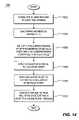
- FIG. 14is a flowchart showing steps of a method for making an interposer in accordance with a preferred embodiment of the present invention.
- the metallic sheet 100may be made of any type of metallic material that provides the desired spring properties. In a preferred embodiment, however, the metallic sheet 100 is stainless steel.
- the metallic sheetmay be of any shape, size, and/or thickness as desired. That is, while a square sheet 100 is shown purely by way of example, the interposer of the present invention may be utilized in a wide variety of applications between a wide variety of devices and may be adapted as appropriate depending on the application and devices and any other relevant considerations.
- the thickness of the metallic sheet 100is approximately 0.004 inches, but may vary depending on the spring characteristics that are desired at the spring members 102 and/or the flexibility desired in the sheet 100 itself.
- the metallic sheet 100is configured to include a plurality of contact supports 101 each having at least two spring members 102 a, 102 b and at least one clearance opening 104 . While two spring members 102 a, 102 b per contact support 101 are shown for purposes of explaining the present invention, a contact support 101 may include any number of spring members. Similarly, while sixteen contact supports 101 are shown for purposes of explaining the present invention, the metallic sheet 100 may include any number of contact supports 101 , depending on the particular application. Additionally, while two openings 104 are shown for purposes of explaining the present invention, only one is necessary to allow for electrical connectivity within a contact.
- having two or more openingsallows an extra connection to be provided between the contacts formed on the spring members 102 a, 102 b, described in detail below, such that if one connection fails, connectivity is maintained.
- additional openingsmay be included to provide multiple circuits at a single contact.
- a single spring membermay be utilized on one side wherein electrical connectivity is provided by electrically connecting the spring member to a via having a solder ball or other type of connector on the other side.
- the spring members 102 a, 102 b and opening(s) 104may be defined on the metallic sheet 100 utilizing any process known to those skilled in the art. Purely by way of example, a chemical etching process may be used.
- the spring members 102 a, 102 bare preferably at least partially disposed downward and upward, as shown in FIG. 3 , for example.
- pressureis applied. Purely be way of example, pressure may be applied by punching, stamping, or any other suitable forming process.
- two spring members 102 a, 102 b and two openings 104are, in one embodiment, provided at each contact support 101 .
- the openingsare shown purely for convenience near the base of spring members 102 a, 102 b. However, it is important to note that not only can any number of openings be provided, but such openings may be provided at any location whatsoever on sheet 100 .
- the location of openings 104is shown near the base of spring members 102 a, 102 b by way of example and to simplify the explanation below regarding how connectivity is provided within the contacts.
- the spring members 102 a, 102 bextend up from a base formed integral with the metallic sheet 100 to a distal end that is configured to have a contact support region, which purely by way of example may be at an apex of a spring member, at what will be a point of contact between the contact that is formed and whatever device is above or below the interposer.
- a contact support regionwhich purely by way of example may be at an apex of a spring member, at what will be a point of contact between the contact that is formed and whatever device is above or below the interposer.
- FIG. 4a cross-sectional view of contact supports 101 is shown.
- the insulative sheet 500may be made of any type of insulative material, as desired.
- the insulative sheet 500is made of Mylar®.
- the insulative sheet 500may be made in any size, shape, and/or thickness, as desired. It is noted, however, that the thinner the insulative sheet 500 , the less likely the insulative sheet 500 is to interfere with the spring properties of the spring members 102 of the metallic sheet 100 .
- the insulative sheet 500is configured with flaps 502 as shown in FIG. 6 .
- vias 510are also defined in sheet 500 .
- the vias 510preferably correspond to the clearance openings 104 in the metallic sheet 100 .
- the diameter of the vias 510is less than the diameter of the clearance openings 104 .
- the flaps 502 and vias 510may be defined on sheet 500 using any process known to those skilled in the art. Purely by way of example, the flaps 502 and vias 510 may be die cut. It is noted that the shape of the flaps 502 may be any shape. For example, the flaps 502 shown in FIG.
- the shape of the flaps 502 in FIGS. 6 , 7 , and 10are slightly oversized.
- the shapemay vary as desired, as long as the hinge point of the flap 502 approximately coincides with the base of the flap's 502 corresponding spring member 102 , and the location at which conductive material is applied to form a contact area on the flap 502 approximately coincides with a peak of the corresponding spring member 102 .
- conductive materialis applied to sheet 500 to form and provide connectivity for each contact.
- the conductive materialwhich purely by way of example may be a gold or gold alloy, is preferably applied at a location that approximately corresponds to what will be the contact support region of the contact once the sheet 500 is placed on the metallic sheet 100 , as shown in FIGS. 7 and 8 . Still referring to FIG. 6 , the conductive material at this location forms a contact area 504 in the shape of a dot (hereinafter “dot 504 ”).
- the conductive materialalso preferably extends in the form of a conductive trace 506 from the dot 504 to at least one via 510 in the sheet 500 that approximately corresponds to a clearance opening 104 in the metallic sheet 100 .
- conductive materialmay be applied on insulative sheet 500 so that it runs from the contact support region to one or more vias 510 provided in the insulative sheet 500 .
- the conductive materialis connected from the dot 504 to two vias 510 in the insulative sheet 500 .
- insulative sheet 500 a, 500 bare applied to metallic sheet 100 to create a flexible bond.
- the spring members 102 a, 102 b of metallic sheet 100force the flaps 502 to detach from the insulative sheet 500 a, 500 b except at approximately the base of the flap 502 so that the flaps 502 rest atop the spring members 102 a, 102 b to which they correspond.
- the insulative sheet 500 a, 500 bmay be attached to the metallic sheet 100 in any manner desired. That is, the insulative sheet 500 a, 500 b may be fixedly or releasably attached to metallic sheet 100 .
- the insulative sheet 500 a, 500 bmay be laminated or otherwise glued to the metallic sheet 100 .
- the insulative sheet 500 a, 500 bmay be heated thereby causing a bond with the metallic sheet 100 or it may be applied to the metallic sheet 100 using pressure adhesives or heat adhesives.
- no adhesivesare necessary where the top and bottom sheets are attached to each other at the vias 510 or along their respective perimeter edges.
- FIG. 9a cross-sectional view of a metallic sheet 100 having an insulative sheet 500 a, 500 b applied to its bottom and top surface to form the interposer of the present invention is shown.
- the cross-sectional viewis taken along line 9 — 9 of FIG. 8 .
- the flaps 502 a, 502 b of the insulative sheet 500 a, 500 blay on top of spring members 102 a, 102 b.
- the sheet 500 a, 500 bis selectively placed such that the conductive material at the point of contact, shown purely for convenience in the form of a dot 504 , is placed approximately at the contact support region of its respective spring member. Further, once the sheet 500 a, 500 b is in place, the vias 510 in the sheet 500 a, 500 b approximately correspond to openings 104 in the metallic sheet 100 .
- the spring members 102 a, 102 bare configured to accommodate variations in the surface of devices with which the interposer is in contact, while maintaining electrical connectivity.
- FIG. 10an exploded view of a contact support 101 of metallic sheet 100 is shown having an insulative sheet 500 b, 500 a being applied to its top and bottom surface to form a contact.
- conductive materialis applied to the insulative sheet 500 a, 500 b at flap 502 a, 502 b in the form of a dot 504 at a point approximately corresponding to the contact support region of the flap's respective spring member. That is, for example, conductive dot 504 on sheet 500 b approximately corresponds to the contact support region of spring member 102 b and the conductive dot 504 placed on sheet 500 a approximately corresponds to the contact support region of spring member 102 a.
- a trace of the conductive material 506 a, 506 bis also run from the respective dot 504 to at least one via 510 a, 510 b.
- the conductive materialis run to two vias.
- a contact 700 formed in accordance with the first preferred embodimentis shown. It is important to note that when the sheets 500 a, 500 b are applied to the metallic sheet 100 , the sheets 500 a, 500 b are pinched at the openings 104 so that electricity running through the contact 700 is insulated from the metallic sheet 100 .
- the sheets 500 a, 500 bmay be heat sealed or attached with an adhesive.
- openings 104may be coated with an insulative material prior to through-plating (described below) or an insulative material may be applied subsequent to applying the insulative sheets 500 a, 500 b to metallic sheet 100 .
- a coating or layer of an insulative oxidemay be applied to the metallic sheet 100 so that it does not become electrically conductive.
- Application of an insulative oxide to the metallic sheet 100may also help the adhesion of the insulative material to the metallic sheet 100 .
- a conductive material 602is plated-through each via 510 and its corresponding clearance opening 104 so that an electrical connection is made with the respective trace 506 a, 506 b.
- the opening 104may be referred to as a conductive via.
- the conductive material utilized in the present inventionmay be any type of conductive material, as desired.
- the conductive materialis a gold or gold alloy.
- insulative sheet 500 ais applied to the metallic sheet 100 in the same direction that insulative sheet 500 b is.
- a single clearance opening 104is provided in metallic sheet 100 and a single via 510 a, 510 b is provided in insulative sheets 500 a, 500 b.
- a conductive trace 506 ais applied from dot 504 to via 510 a.
- a conductive trace 506 bis applied from dot 504 to via 510 b.
- a method 1000is shown for making an interposer in accordance with the present invention.
- the method 1000begins in step 1002 with defining contact supports having at least two spring members and defining at least one clearance opening in a metallic sheet.
- step 1004at each contact support in a metallic sheet, at least one spring member is biased upwardly and at least one spring is biased downwardly to form upward and downward biased spring members.
- the spring membersmay be formed so that they are biased in a particular direction by applying pressure to the member in the desired direction.
- step 1006flaps and vias are die cut or otherwise defined in a sheet of insulative material.
- the flaps of the insulative sheetpreferably approximately correspond in shape and location to spring members in the metallic sheet.
- the vias of the insulative sheetpreferably approximately correspond to openings in the metallic sheet.
- conductive materialis added to the insulative sheet so that the conductive material is configured to provide a contact point at locations of the insulative sheet that approximately correspond to the contact support region of spring members of a metallic sheet on which the insulative sheet will be applied.
- the conductive materialpreferably runs from the contact point to at least one via in the insulative sheet that approximately corresponds to an opening in a metallic sheet. It is important to note that step 1008 may be performed prior to step 1006 .
- step 1010the insulative sheet is applied to the top and bottom surface of the metallic sheet to form the interposer of the present invention.
- step 1012the top and bottom sheets are connected at the least one via and the via is plated-through with a conductive material. This completes the circuit(s) between the at least two points of contact for each contact provided in the interposer.
- stepsmay be performed in any order as desired. That is, the particular ordering of the steps shown in FIG. 14 is for convenience in explaining the present invention.
- application of conductive material to the insulative sheetmay be performed subsequent to applying the insulative sheet to the metallic sheet and plating-through the via(s).
- steps related to defining elements of the metallic and insulative sheetsmay of course be performed at any time with respect to each other including the simultaneous performance thereof.
Landscapes
- Measuring Leads Or Probes (AREA)
Abstract
Description
Claims (7)
Priority Applications (1)
| Application Number | Priority Date | Filing Date | Title |
|---|---|---|---|
| US10/884,709US7025601B2 (en) | 2004-03-19 | 2004-07-02 | Interposer and method for making same |
Applications Claiming Priority (2)
| Application Number | Priority Date | Filing Date | Title |
|---|---|---|---|
| US55482004P | 2004-03-19 | 2004-03-19 | |
| US10/884,709US7025601B2 (en) | 2004-03-19 | 2004-07-02 | Interposer and method for making same |
Publications (2)
| Publication Number | Publication Date |
|---|---|
| US20050208786A1 US20050208786A1 (en) | 2005-09-22 |
| US7025601B2true US7025601B2 (en) | 2006-04-11 |
Family
ID=34986932
Family Applications (1)
| Application Number | Title | Priority Date | Filing Date |
|---|---|---|---|
| US10/884,709Expired - LifetimeUS7025601B2 (en) | 2004-03-19 | 2004-07-02 | Interposer and method for making same |
Country Status (1)
| Country | Link |
|---|---|
| US (1) | US7025601B2 (en) |
Cited By (28)
| Publication number | Priority date | Publication date | Assignee | Title |
|---|---|---|---|---|
| US20050164527A1 (en)* | 2003-04-11 | 2005-07-28 | Radza Eric M. | Method and system for batch forming spring elements in three dimensions |
| US20050208788A1 (en)* | 2004-03-19 | 2005-09-22 | Dittmann Larry E | Electrical connector in a flexible host |
| US20050205988A1 (en)* | 2004-03-19 | 2005-09-22 | Epic Technology Inc. | Die package with higher useable die contact pad area |
| US20050204538A1 (en)* | 2004-03-19 | 2005-09-22 | Epic Technology Inc. | Contact and method for making same |
| US20060189179A1 (en)* | 2003-04-11 | 2006-08-24 | Neoconix Inc. | Flat flex cable (FFC) with embedded spring contacts for connecting to a PCB or like electronic device |
| US20060258183A1 (en)* | 2003-04-11 | 2006-11-16 | Neoconix, Inc. | Electrical connector on a flexible carrier |
| US20060258182A1 (en)* | 2004-07-20 | 2006-11-16 | Dittmann Larry E | Interposer with compliant pins |
| US20070020960A1 (en)* | 2003-04-11 | 2007-01-25 | Williams John D | Contact grid array system |
| US20070050738A1 (en)* | 2005-08-31 | 2007-03-01 | Dittmann Larry E | Customer designed interposer |
| US20070054515A1 (en)* | 2003-04-11 | 2007-03-08 | Williams John D | Method for fabricating a contact grid array |
| US20070134949A1 (en)* | 2005-12-12 | 2007-06-14 | Dittmann Larry E | Connector having staggered contact architecture for enhanced working range |
| US20070218710A1 (en)* | 2003-06-11 | 2007-09-20 | Brown Dirk D | Structure and process for a contact grid array formed in a circuitized substrate |
| US20070259539A1 (en)* | 2003-04-11 | 2007-11-08 | Brown Dirk D | Method and system for batch manufacturing of spring elements |
| US20070275572A1 (en)* | 2003-12-08 | 2007-11-29 | Williams John D | Connector for making electrical contact at semiconductor scales |
| US20090025739A1 (en)* | 2007-07-23 | 2009-01-29 | R. J. Reynolds Tobacco Company | Smokeless Tobacco Composition |
| US20090181559A1 (en)* | 2008-01-10 | 2009-07-16 | Tyco Electronics Corporation | Laminated electrical contact strip |
| US20090317986A1 (en)* | 2007-06-26 | 2009-12-24 | Chia-Pin Chiu | Skived electrical contact for connecting an ic device to a circuit board and method of making a contact by skiving |
| US7891984B1 (en)* | 2010-01-29 | 2011-02-22 | Lotes Co., Ltd. | Electrical connector |
| US20120089002A1 (en)* | 2009-07-01 | 2012-04-12 | Koninklijke Philips Electronics N.V. | Low cost-low profile lead set connector |
| US8215966B2 (en) | 2010-04-20 | 2012-07-10 | Tyco Electronics Corporation | Interposer connector assembly |
| US20130330945A1 (en)* | 2012-06-07 | 2013-12-12 | Hon Hai Precision Industry Co., Ltd. | Electrical connector assembly with an adaptor for electrical connecting the electrical connector and the pcb |
| US8641428B2 (en) | 2011-12-02 | 2014-02-04 | Neoconix, Inc. | Electrical connector and method of making it |
| CN104733976A (en)* | 2013-12-23 | 2015-06-24 | 欣兴电子股份有限公司 | Connector and manufacturing method thereof |
| US9680273B2 (en) | 2013-03-15 | 2017-06-13 | Neoconix, Inc | Electrical connector with electrical contacts protected by a layer of compressible material and method of making it |
| US11211728B2 (en) | 2019-01-14 | 2021-12-28 | Amphenol Corporation | Midboard cable terminology assembly |
| US11404811B2 (en)* | 2019-01-14 | 2022-08-02 | Amphenol Corporation | Small form factor interposer |
| US11476619B2 (en) | 2018-07-20 | 2022-10-18 | Fci Usa Llc | High frequency connector with kick-out |
| US11670879B2 (en) | 2020-01-28 | 2023-06-06 | Fci Usa Llc | High frequency midboard connector |
Families Citing this family (10)
| Publication number | Priority date | Publication date | Assignee | Title |
|---|---|---|---|---|
| US7331797B1 (en)* | 2006-07-26 | 2008-02-19 | Lotes Co., Ltd. | Electrical connector and a manufacturing method thereof |
| USD574776S1 (en)* | 2007-08-09 | 2008-08-12 | Solarwatt Ag | Omega-connector |
| USD579414S1 (en)* | 2007-08-09 | 2008-10-28 | Solar Watt Ag | E-connector |
| USD574777S1 (en)* | 2007-08-09 | 2008-08-12 | Solarwatt Ag | C-connector |
| JP5313156B2 (en)* | 2007-10-19 | 2013-10-09 | 日本発條株式会社 | Connection terminals, semiconductor packages, wiring boards, connectors, and micro contactors |
| USD577676S1 (en)* | 2007-11-26 | 2008-09-30 | Solarwatt Ag | Z-connector |
| US8109769B1 (en)* | 2010-12-17 | 2012-02-07 | Rogue Valley Microdevices | Micromachined flex interposers |
| DE102013213497A1 (en)* | 2013-05-24 | 2014-11-27 | Continental Teves Ag & Co. Ohg | Method for producing a contact element, contact element and its use |
| CN109599696A (en)* | 2017-09-28 | 2019-04-09 | 富士康(昆山)电脑接插件有限公司 | Electric connector |
| US10980135B2 (en)* | 2019-02-18 | 2021-04-13 | John O. Tate | Insulated socket body and terminals for a land grid array socket assembly |
Citations (126)
| Publication number | Priority date | Publication date | Assignee | Title |
|---|---|---|---|---|
| US3543587A (en) | 1967-10-07 | 1970-12-01 | Tokyo Keiki Kk | Gyroscopic instrument |
| US3634807A (en) | 1969-03-28 | 1972-01-11 | Siemens Ag | Detachable electrical contact arrangement |
| US3670409A (en) | 1970-11-19 | 1972-06-20 | Gte Automatic Electric Lab Inc | Planar receptacle |
| US4548451A (en)* | 1984-04-27 | 1985-10-22 | International Business Machines Corporation | Pinless connector interposer and method for making the same |
| US4893172A (en) | 1987-01-19 | 1990-01-09 | Hitachi, Ltd. | Connecting structure for electronic part and method of manufacturing the same |
| US4998885A (en) | 1989-10-27 | 1991-03-12 | International Business Machines Corporation | Elastomeric area array interposer |
| US5152695A (en) | 1991-10-10 | 1992-10-06 | Amp Incorporated | Surface mount electrical connector |
| US5173055A (en) | 1991-08-08 | 1992-12-22 | Amp Incorporated | Area array connector |
| US5199879A (en) | 1992-02-24 | 1993-04-06 | International Business Machines Corporation | Electrical assembly with flexible circuit |
| US5228861A (en) | 1992-06-12 | 1993-07-20 | Amp Incorporated | High density electrical connector system |
| US5257950A (en) | 1991-07-17 | 1993-11-02 | The Whitaker Corporation | Filtered electrical connector |
| US5292558A (en) | 1991-08-08 | 1994-03-08 | University Of Texas At Austin, Texas | Process for metal deposition for microelectronic interconnections |
| US5299939A (en)* | 1992-03-05 | 1994-04-05 | International Business Machines Corporation | Spring array connector |
| US5358411A (en) | 1993-08-09 | 1994-10-25 | The Whitaker Corporation | Duplex plated epsilon compliant beam contact and interposer |
| US5366380A (en) | 1989-06-13 | 1994-11-22 | General Datacomm, Inc. | Spring biased tapered contact elements for electrical connectors and integrated circuit packages |
| US5468655A (en) | 1994-10-31 | 1995-11-21 | Motorola, Inc. | Method for forming a temporary attachment between a semiconductor die and a substrate using a metal paste comprising spherical modules |
| US5483741A (en) | 1993-09-03 | 1996-01-16 | Micron Technology, Inc. | Method for fabricating a self limiting silicon based interconnect for testing bare semiconductor dice |
| WO1996002068A1 (en) | 1994-07-07 | 1996-01-25 | Tessera, Inc. | Microelectronic mounting with multiple lead deformation |
| US5530288A (en) | 1994-10-12 | 1996-06-25 | International Business Machines Corporation | Passive interposer including at least one passive electronic component |
| US5532612A (en) | 1994-07-19 | 1996-07-02 | Liang; Louis H. | Methods and apparatus for test and burn-in of integrated circuit devices |
| US5590460A (en) | 1994-07-19 | 1997-01-07 | Tessera, Inc. | Method of making multilayer circuit |
| US5593903A (en) | 1996-03-04 | 1997-01-14 | Motorola, Inc. | Method of forming contact pads for wafer level testing and burn-in of semiconductor dice |
| US5629837A (en) | 1995-09-20 | 1997-05-13 | Oz Technologies, Inc. | Button contact for surface mounting an IC device to a circuit board |
| US5632631A (en) | 1994-06-07 | 1997-05-27 | Tessera, Inc. | Microelectronic contacts with asperities and methods of making same |
| WO1997044859A1 (en) | 1996-05-24 | 1997-11-27 | Tessera, Inc. | Connectors for microelectronic elements |
| US5772451A (en) | 1993-11-16 | 1998-06-30 | Form Factor, Inc. | Sockets for electronic components and methods of connecting to electronic components |
| US5791911A (en) | 1996-10-25 | 1998-08-11 | International Business Machines Corporation | Coaxial interconnect devices and methods of making the same |
| US5802699A (en) | 1994-06-07 | 1998-09-08 | Tessera, Inc. | Methods of assembling microelectronic assembly with socket for engaging bump leads |
| US5842273A (en) | 1996-01-26 | 1998-12-01 | Hewlett-Packard Company | Method of forming electrical interconnects using isotropic conductive adhesives and connections formed thereby |
| US5860585A (en) | 1996-05-31 | 1999-01-19 | Motorola, Inc. | Substrate for transferring bumps and method of use |
| US5896038A (en) | 1996-11-08 | 1999-04-20 | W. L. Gore & Associates, Inc. | Method of wafer level burn-in |
| US5967797A (en) | 1997-09-24 | 1999-10-19 | Teledyne Industries, Inc. | High density multi-pin connector with solder points |
| US5980335A (en) | 1998-03-27 | 1999-11-09 | Molex Incorporated | Electrical terminal |
| US5989994A (en) | 1998-12-29 | 1999-11-23 | Advantest Corp. | Method for producing contact structures |
| JP2000011443A (en) | 1998-04-21 | 2000-01-14 | Nec Corp | Optical module device, combined prism using it, and forming method thereof |
| US6019611A (en) | 1998-02-12 | 2000-02-01 | Hon Hai Precision Ind. Co., Ltd. | Land grid array assembly and related contact |
| US6031282A (en) | 1998-08-27 | 2000-02-29 | Advantest Corp. | High performance integrated circuit chip package |
| US6032356A (en) | 1993-11-16 | 2000-03-07 | Formfactor. Inc. | Wafer-level test and burn-in, and semiconductor process |
| US6042387A (en) | 1998-03-27 | 2000-03-28 | Oz Technologies, Inc. | Connector, connector system and method of making a connector |
| US6063640A (en) | 1997-03-18 | 2000-05-16 | Fujitsu Limited | Semiconductor wafer testing method with probe pin contact |
| US6083837A (en) | 1996-12-13 | 2000-07-04 | Tessera, Inc. | Fabrication of components by coining |
| US6133534A (en) | 1991-11-29 | 2000-10-17 | Hitachi Chemical Company, Ltd. | Wiring board for electrical tests with bumps having polymeric coating |
| US6146151A (en) | 1999-08-18 | 2000-11-14 | Hon Hai Precision Ind. Co., Ltd. | Method for forming an electrical connector and an electrical connector obtained by the method |
| US6156484A (en) | 1997-11-07 | 2000-12-05 | International Business Machines Corporation | Gray scale etching for thin flexible interposer |
| US6184699B1 (en) | 1995-06-07 | 2001-02-06 | Xerox Corporation | Photolithographically patterned spring contact |
| US6196852B1 (en) | 1997-04-02 | 2001-03-06 | Siemens Nixdorf Informationssysteme Aktiengesellschaft | Contact arrangement |
| US6200143B1 (en) | 1998-01-09 | 2001-03-13 | Tessera, Inc. | Low insertion force connector for microelectronic elements |
| US6204065B1 (en) | 1997-03-27 | 2001-03-20 | Ngk Insulators, Ltd. | Conduction assist member and manufacturing method of the same |
| US6208157B1 (en) | 1997-08-22 | 2001-03-27 | Micron Technology, Inc. | Method for testing semiconductor components |
| US6221750B1 (en) | 1998-10-28 | 2001-04-24 | Tessera, Inc. | Fabrication of deformable leads of microelectronic elements |
| US6224392B1 (en) | 1998-12-04 | 2001-05-01 | International Business Machines Corporation | Compliant high-density land grid array (LGA) connector and method of manufacture |
| US6250933B1 (en) | 2000-01-20 | 2001-06-26 | Advantest Corp. | Contact structure and production method thereof |
| US6255727B1 (en) | 1999-08-03 | 2001-07-03 | Advantest Corp. | Contact structure formed by microfabrication process |
| JP2001203435A (en) | 2000-01-21 | 2001-07-27 | Ibiden Co Ltd | Connection structure of ball grid array type package |
| US6293808B1 (en) | 1999-09-30 | 2001-09-25 | Ngk Insulators, Ltd. | Contact sheet |
| US6293806B1 (en) | 2000-02-02 | 2001-09-25 | Hon Hai Precision Ind. Co., Ltd. | Electrical connector with improved terminals for electrically connecting to a circuit board |
| US6297164B1 (en) | 1998-11-30 | 2001-10-02 | Advantest Corp. | Method for producing contact structures |
| US6298552B1 (en) | 2000-02-10 | 2001-10-09 | Hon Hai Precision Ind. Co., Ltd. | Method for making socket connector |
| US6306752B1 (en) | 1998-09-15 | 2001-10-23 | Tessera, Inc. | Connection component and method of making same |
| US6335210B1 (en) | 1999-12-17 | 2002-01-01 | International Business Machines Corporation | Baseplate for chip burn-in and/of testing, and method thereof |
| US6336269B1 (en) | 1993-11-16 | 2002-01-08 | Benjamin N. Eldridge | Method of fabricating an interconnection element |
| US6337575B1 (en) | 1998-12-23 | 2002-01-08 | Micron Technology, Inc. | Methods of testing integrated circuitry, methods of forming tester substrates, and circuitry testing substrates |
| US20020011859A1 (en) | 1993-12-23 | 2002-01-31 | Kenneth R. Smith | Method for forming conductive bumps for the purpose of contrructing a fine pitch test device |
| WO2002013253A1 (en) | 2000-08-03 | 2002-02-14 | David Frank Moore | Microconnectors and method for their production |
| US6361328B1 (en) | 1999-08-03 | 2002-03-26 | Framatome Connectors International | Surface-mounted low profile connector |
| US6373267B1 (en) | 1997-05-30 | 2002-04-16 | Ando Electric Company | Ball grid array-integrated circuit testing device |
| US20020055282A1 (en) | 2000-11-09 | 2002-05-09 | Eldridge Benjamin N. | Electronic components with plurality of contoured microelectronic spring contacts |
| US20020058356A1 (en) | 1998-04-16 | 2002-05-16 | Yoichi Oya | Semiconductor package and mount board, and mounting method using the same |
| US6392524B1 (en) | 2000-06-09 | 2002-05-21 | Xerox Corporation | Photolithographically-patterned out-of-plane coil structures and method of making |
| US6392534B1 (en) | 1996-08-22 | 2002-05-21 | Kenneth E. Flick | Remote control system for a vehicle having a data communications bus and related methods |
| US6399900B1 (en) | 1999-04-30 | 2002-06-04 | Advantest Corp. | Contact structure formed over a groove |
| US6402526B1 (en) | 2000-11-03 | 2002-06-11 | Delphi Technologies, Inc. | Microelectronic contact assembly |
| US20020079120A1 (en) | 1999-08-30 | 2002-06-27 | Steven R. Eskildsen | Implementing micro bgatm assembly techniques for small die |
| US6420884B1 (en) | 1999-01-29 | 2002-07-16 | Advantest Corp. | Contact structure formed by photolithography process |
| US6420789B1 (en) | 2000-05-16 | 2002-07-16 | Micron Technology, Inc. | Ball grid array chip packages having improved testing and stacking characteristics |
| US6420661B1 (en) | 1995-09-12 | 2002-07-16 | Tessera, Inc. | Connector element for connecting microelectronic elements |
| US6436802B1 (en) | 1998-11-30 | 2002-08-20 | Adoamtest Corp. | Method of producing contact structure |
| US6437591B1 (en) | 1999-03-25 | 2002-08-20 | Micron Technology, Inc. | Test interconnect for bumped semiconductor components and method of fabrication |
| US6442039B1 (en) | 1999-12-03 | 2002-08-27 | Delphi Technologies, Inc. | Metallic microstructure springs and method of making same |
| US6452407B2 (en) | 1998-06-19 | 2002-09-17 | Advantest Corp. | Probe contactor and production method thereof |
| US20020129894A1 (en) | 2001-01-08 | 2002-09-19 | Kuo-Chuan Liu | Method for joining and an ultra-high density interconnect |
| US20020133941A1 (en) | 1999-03-10 | 2002-09-26 | Salman Akram | Electrical connector |
| US6461892B2 (en) | 2000-01-26 | 2002-10-08 | Tessera, Inc. | Methods of making a connection component using a removable layer |
| US20020146919A1 (en) | 2000-12-29 | 2002-10-10 | Cohn Michael B. | Micromachined springs for strain relieved electrical connections to IC chips |
| US6474997B1 (en) | 1999-09-30 | 2002-11-05 | Ngk Insulators, Ltd. | Contact sheet |
| US20020178331A1 (en) | 1999-04-23 | 2002-11-28 | Beardsley Brent Cameron | Prestaging data into cache in preparation for data transfer operations |
| US6492251B1 (en) | 1999-03-10 | 2002-12-10 | Tessera, Inc. | Microelectronic joining processes with bonding material application |
| US20030003779A1 (en)* | 2000-01-20 | 2003-01-02 | Rathburn James J | Flexible compliant interconnect assembly |
| US6517362B2 (en) | 2000-09-26 | 2003-02-11 | Yukihiro Hirai | Spiral contactor, semiconductor device inspecting apparatus and electronic part using same, and method of manufacturing the same |
| US6520778B1 (en) | 1997-02-18 | 2003-02-18 | Formfactor, Inc. | Microelectronic contact structures, and methods of making same |
| EP0692823B1 (en) | 1994-07-11 | 2003-02-19 | Sun Microsystems, Inc. | Ball grid array package for an integated circuit and method of reducing ground bounce |
| US20030035277A1 (en) | 2001-07-13 | 2003-02-20 | Saputro Stephanus D. | Reducing inductance of a capacitor |
| US6524115B1 (en) | 1999-08-20 | 2003-02-25 | 3M Innovative Properties Company | Compliant interconnect assembly |
| US6551112B1 (en) | 2002-03-18 | 2003-04-22 | High Connection Density, Inc. | Test and burn-in connector |
| US20030089936A1 (en) | 2001-11-13 | 2003-05-15 | Mccormack Mark Thomas | Structure and method for embedding capacitors in Z-connected multi-chip modules |
| US20030096512A1 (en) | 2001-06-14 | 2003-05-22 | Christopher Cornell | Electrical interconnect device incorporating anisotropically conductive elastomer and flexible circuit |
| US20030099097A1 (en) | 2001-11-27 | 2003-05-29 | Sammy Mok | Construction structures and manufacturing processes for probe card assemblies and packages having wafer level springs |
| US6576485B2 (en) | 1998-11-30 | 2003-06-10 | Advantest Corp. | Contact structure and production method thereof and probe contact assembly using same |
| US20030129866A1 (en) | 2002-01-07 | 2003-07-10 | Romano Linda T. | Spring metal structure with passive-conductive coating on tip |
| US20030147197A1 (en) | 2000-03-15 | 2003-08-07 | Kazuhide Uriu | Multilayer electronic part, multilayer antenna duplexer, and communication apparatus |
| US6604950B2 (en) | 2001-04-26 | 2003-08-12 | Teledyne Technologies Incorporated | Low pitch, high density connector |
| US6612861B2 (en) | 2000-02-14 | 2003-09-02 | Advantest Corp. | Contact structure and production method thereof |
| US6616966B2 (en) | 1998-12-02 | 2003-09-09 | Formfactor, Inc. | Method of making lithographic contact springs |
| US6622380B1 (en) | 2002-02-12 | 2003-09-23 | Micron Technology, Inc. | Methods for manufacturing microelectronic devices and methods for mounting microelectronic packages to circuit boards |
| US6627092B2 (en) | 2001-07-27 | 2003-09-30 | Hewlett-Packard Development Company, L.P. | Method for the fabrication of electrical contacts |
| US20030194832A1 (en) | 2001-09-26 | 2003-10-16 | Lopata John E.. | Power delivery system for integrated circuits utilizing discrete capacitors |
| US6640432B1 (en) | 2000-04-12 | 2003-11-04 | Formfactor, Inc. | Method of fabricating shaped springs |
| US6661247B2 (en) | 1997-09-19 | 2003-12-09 | Fujitsu Limited | Semiconductor testing device |
| US6664131B2 (en) | 1999-07-13 | 2003-12-16 | Micron Technology, Inc. | Method of making ball grid array package with deflectable interconnect |
| US6671947B2 (en) | 1999-06-28 | 2004-01-06 | Intel Corporation | Method of making an interposer |
| US6677245B2 (en) | 1998-11-30 | 2004-01-13 | Advantest Corp. | Contact structure production method |
| US6692263B2 (en)* | 2000-10-02 | 2004-02-17 | Alcatel | Spring connector for electrically connecting tracks of a display screen with an electrical circuit |
| US6700072B2 (en) | 1996-12-13 | 2004-03-02 | Tessera, Inc. | Electrical connection with inwardly deformable contacts |
| US6719569B2 (en)* | 2001-10-02 | 2004-04-13 | Ngk Insulators, Ltd. | Contact sheet for providing an electrical connection between a plurality of electronic devices |
| US6730134B2 (en) | 2001-07-02 | 2004-05-04 | Intercon Systems, Inc. | Interposer assembly |
| US6736665B2 (en) | 1998-11-30 | 2004-05-18 | Advantest Corp. | Contact structure production method |
| US6750136B2 (en) | 1998-11-30 | 2004-06-15 | Advantest Corp. | Contact structure production method |
| US20040118603A1 (en) | 2002-12-18 | 2004-06-24 | Chambers Douglas C. | Methods and apparatus for a flexible circuit interposer |
| US20040127073A1 (en)* | 2002-12-27 | 2004-07-01 | Ngk Insulators, Ltd. | Contact sheet, method of manufacturing the same and socket including the same |
| US6791171B2 (en) | 2000-06-20 | 2004-09-14 | Nanonexus, Inc. | Systems for testing and packaging integrated circuits |
| US6815961B2 (en) | 1999-07-28 | 2004-11-09 | Nanonexus, Inc. | Construction structures and manufacturing processes for integrated circuit wafer probe card assemblies |
| EP1208241B1 (en) | 2000-04-04 | 2005-01-12 | Fundacao Oswaldo Cruz - Fiocruz | Method and kit for the detection of schistosomiasis through the polymerase chain reaction |
| US6847101B2 (en) | 1995-10-31 | 2005-01-25 | Tessera, Inc. | Microelectronic package having a compliant layer with bumped protrusions |
| US6848173B2 (en) | 1994-07-07 | 2005-02-01 | Tessera, Inc. | Microelectric packages having deformed bonded leads and methods therefor |
| US6857880B2 (en)* | 2001-11-09 | 2005-02-22 | Tomonari Ohtsuki | Electrical connector |
| US20050099193A1 (en) | 2003-11-07 | 2005-05-12 | Jeff Burgess | Electronic component/interface interposer |
Family Cites Families (2)
| Publication number | Priority date | Publication date | Assignee | Title |
|---|---|---|---|---|
| US6452409B1 (en)* | 2000-06-08 | 2002-09-17 | Advanced Micro Devices, Inc. | Mechanism that holds down packages |
| US6481467B2 (en)* | 2001-03-15 | 2002-11-19 | Band-It-Idex, Inc. | Powered band clamping under electrical control |
- 2004
- 2004-07-02USUS10/884,709patent/US7025601B2/ennot_activeExpired - Lifetime
Patent Citations (133)
| Publication number | Priority date | Publication date | Assignee | Title |
|---|---|---|---|---|
| US3543587A (en) | 1967-10-07 | 1970-12-01 | Tokyo Keiki Kk | Gyroscopic instrument |
| US3634807A (en) | 1969-03-28 | 1972-01-11 | Siemens Ag | Detachable electrical contact arrangement |
| US3670409A (en) | 1970-11-19 | 1972-06-20 | Gte Automatic Electric Lab Inc | Planar receptacle |
| US4548451A (en)* | 1984-04-27 | 1985-10-22 | International Business Machines Corporation | Pinless connector interposer and method for making the same |
| US4893172A (en) | 1987-01-19 | 1990-01-09 | Hitachi, Ltd. | Connecting structure for electronic part and method of manufacturing the same |
| US5366380A (en) | 1989-06-13 | 1994-11-22 | General Datacomm, Inc. | Spring biased tapered contact elements for electrical connectors and integrated circuit packages |
| US4998885A (en) | 1989-10-27 | 1991-03-12 | International Business Machines Corporation | Elastomeric area array interposer |
| US5257950A (en) | 1991-07-17 | 1993-11-02 | The Whitaker Corporation | Filtered electrical connector |
| US5292558A (en) | 1991-08-08 | 1994-03-08 | University Of Texas At Austin, Texas | Process for metal deposition for microelectronic interconnections |
| US5173055A (en) | 1991-08-08 | 1992-12-22 | Amp Incorporated | Area array connector |
| US5152695A (en) | 1991-10-10 | 1992-10-06 | Amp Incorporated | Surface mount electrical connector |
| US6133534A (en) | 1991-11-29 | 2000-10-17 | Hitachi Chemical Company, Ltd. | Wiring board for electrical tests with bumps having polymeric coating |
| US5199879A (en) | 1992-02-24 | 1993-04-06 | International Business Machines Corporation | Electrical assembly with flexible circuit |
| US5299939A (en)* | 1992-03-05 | 1994-04-05 | International Business Machines Corporation | Spring array connector |
| US5228861A (en) | 1992-06-12 | 1993-07-20 | Amp Incorporated | High density electrical connector system |
| US5358411A (en) | 1993-08-09 | 1994-10-25 | The Whitaker Corporation | Duplex plated epsilon compliant beam contact and interposer |
| US5483741A (en) | 1993-09-03 | 1996-01-16 | Micron Technology, Inc. | Method for fabricating a self limiting silicon based interconnect for testing bare semiconductor dice |
| US6336269B1 (en) | 1993-11-16 | 2002-01-08 | Benjamin N. Eldridge | Method of fabricating an interconnection element |
| US6032356A (en) | 1993-11-16 | 2000-03-07 | Formfactor. Inc. | Wafer-level test and burn-in, and semiconductor process |
| US5772451A (en) | 1993-11-16 | 1998-06-30 | Form Factor, Inc. | Sockets for electronic components and methods of connecting to electronic components |
| US20020011859A1 (en) | 1993-12-23 | 2002-01-31 | Kenneth R. Smith | Method for forming conductive bumps for the purpose of contrructing a fine pitch test device |
| US5802699A (en) | 1994-06-07 | 1998-09-08 | Tessera, Inc. | Methods of assembling microelectronic assembly with socket for engaging bump leads |
| US5812378A (en) | 1994-06-07 | 1998-09-22 | Tessera, Inc. | Microelectronic connector for engaging bump leads |
| US5632631A (en) | 1994-06-07 | 1997-05-27 | Tessera, Inc. | Microelectronic contacts with asperities and methods of making same |
| US6205660B1 (en) | 1994-06-07 | 2001-03-27 | Tessera, Inc. | Method of making an electronic contact |
| US5934914A (en) | 1994-06-07 | 1999-08-10 | Tessera, Inc. | Microelectronic contacts with asperities and methods of making same |
| WO1996002068A1 (en) | 1994-07-07 | 1996-01-25 | Tessera, Inc. | Microelectronic mounting with multiple lead deformation |
| US6848173B2 (en) | 1994-07-07 | 2005-02-01 | Tessera, Inc. | Microelectric packages having deformed bonded leads and methods therefor |
| EP0692823B1 (en) | 1994-07-11 | 2003-02-19 | Sun Microsystems, Inc. | Ball grid array package for an integated circuit and method of reducing ground bounce |
| US5532612A (en) | 1994-07-19 | 1996-07-02 | Liang; Louis H. | Methods and apparatus for test and burn-in of integrated circuit devices |
| US5590460A (en) | 1994-07-19 | 1997-01-07 | Tessera, Inc. | Method of making multilayer circuit |
| US5530288A (en) | 1994-10-12 | 1996-06-25 | International Business Machines Corporation | Passive interposer including at least one passive electronic component |
| US5468655A (en) | 1994-10-31 | 1995-11-21 | Motorola, Inc. | Method for forming a temporary attachment between a semiconductor die and a substrate using a metal paste comprising spherical modules |
| US6264477B1 (en) | 1995-06-07 | 2001-07-24 | Xerox Corporation | Photolithographically patterned spring contact |
| US6184699B1 (en) | 1995-06-07 | 2001-02-06 | Xerox Corporation | Photolithographically patterned spring contact |
| US6420661B1 (en) | 1995-09-12 | 2002-07-16 | Tessera, Inc. | Connector element for connecting microelectronic elements |
| US5629837A (en) | 1995-09-20 | 1997-05-13 | Oz Technologies, Inc. | Button contact for surface mounting an IC device to a circuit board |
| US6847101B2 (en) | 1995-10-31 | 2005-01-25 | Tessera, Inc. | Microelectronic package having a compliant layer with bumped protrusions |
| US5842273A (en) | 1996-01-26 | 1998-12-01 | Hewlett-Packard Company | Method of forming electrical interconnects using isotropic conductive adhesives and connections formed thereby |
| US5593903A (en) | 1996-03-04 | 1997-01-14 | Motorola, Inc. | Method of forming contact pads for wafer level testing and burn-in of semiconductor dice |
| WO1997044859A1 (en) | 1996-05-24 | 1997-11-27 | Tessera, Inc. | Connectors for microelectronic elements |
| US5860585A (en) | 1996-05-31 | 1999-01-19 | Motorola, Inc. | Substrate for transferring bumps and method of use |
| US6392534B1 (en) | 1996-08-22 | 2002-05-21 | Kenneth E. Flick | Remote control system for a vehicle having a data communications bus and related methods |
| US5791911A (en) | 1996-10-25 | 1998-08-11 | International Business Machines Corporation | Coaxial interconnect devices and methods of making the same |
| US5896038A (en) | 1996-11-08 | 1999-04-20 | W. L. Gore & Associates, Inc. | Method of wafer level burn-in |
| US6700072B2 (en) | 1996-12-13 | 2004-03-02 | Tessera, Inc. | Electrical connection with inwardly deformable contacts |
| US6083837A (en) | 1996-12-13 | 2000-07-04 | Tessera, Inc. | Fabrication of components by coining |
| US6520778B1 (en) | 1997-02-18 | 2003-02-18 | Formfactor, Inc. | Microelectronic contact structures, and methods of making same |
| US6063640A (en) | 1997-03-18 | 2000-05-16 | Fujitsu Limited | Semiconductor wafer testing method with probe pin contact |
| US6204065B1 (en) | 1997-03-27 | 2001-03-20 | Ngk Insulators, Ltd. | Conduction assist member and manufacturing method of the same |
| US6196852B1 (en) | 1997-04-02 | 2001-03-06 | Siemens Nixdorf Informationssysteme Aktiengesellschaft | Contact arrangement |
| US6373267B1 (en) | 1997-05-30 | 2002-04-16 | Ando Electric Company | Ball grid array-integrated circuit testing device |
| US6208157B1 (en) | 1997-08-22 | 2001-03-27 | Micron Technology, Inc. | Method for testing semiconductor components |
| US6661247B2 (en) | 1997-09-19 | 2003-12-09 | Fujitsu Limited | Semiconductor testing device |
| US5967797A (en) | 1997-09-24 | 1999-10-19 | Teledyne Industries, Inc. | High density multi-pin connector with solder points |
| US6156484A (en) | 1997-11-07 | 2000-12-05 | International Business Machines Corporation | Gray scale etching for thin flexible interposer |
| US6374487B1 (en) | 1998-01-09 | 2002-04-23 | Tessera, Inc. | Method of making a connection to a microelectronic element |
| US6428328B2 (en) | 1998-01-09 | 2002-08-06 | Tessera, Inc. | Method of making a connection to a microelectronic element |
| US6200143B1 (en) | 1998-01-09 | 2001-03-13 | Tessera, Inc. | Low insertion force connector for microelectronic elements |
| US6019611A (en) | 1998-02-12 | 2000-02-01 | Hon Hai Precision Ind. Co., Ltd. | Land grid array assembly and related contact |
| US6042387A (en) | 1998-03-27 | 2000-03-28 | Oz Technologies, Inc. | Connector, connector system and method of making a connector |
| US5980335A (en) | 1998-03-27 | 1999-11-09 | Molex Incorporated | Electrical terminal |
| US20020058356A1 (en) | 1998-04-16 | 2002-05-16 | Yoichi Oya | Semiconductor package and mount board, and mounting method using the same |
| JP2000011443A (en) | 1998-04-21 | 2000-01-14 | Nec Corp | Optical module device, combined prism using it, and forming method thereof |
| US6452407B2 (en) | 1998-06-19 | 2002-09-17 | Advantest Corp. | Probe contactor and production method thereof |
| US6031282A (en) | 1998-08-27 | 2000-02-29 | Advantest Corp. | High performance integrated circuit chip package |
| US6306752B1 (en) | 1998-09-15 | 2001-10-23 | Tessera, Inc. | Connection component and method of making same |
| US6221750B1 (en) | 1998-10-28 | 2001-04-24 | Tessera, Inc. | Fabrication of deformable leads of microelectronic elements |
| US6297164B1 (en) | 1998-11-30 | 2001-10-02 | Advantest Corp. | Method for producing contact structures |
| US6576485B2 (en) | 1998-11-30 | 2003-06-10 | Advantest Corp. | Contact structure and production method thereof and probe contact assembly using same |
| US6677245B2 (en) | 1998-11-30 | 2004-01-13 | Advantest Corp. | Contact structure production method |
| US6736665B2 (en) | 1998-11-30 | 2004-05-18 | Advantest Corp. | Contact structure production method |
| US6436802B1 (en) | 1998-11-30 | 2002-08-20 | Adoamtest Corp. | Method of producing contact structure |
| US6750136B2 (en) | 1998-11-30 | 2004-06-15 | Advantest Corp. | Contact structure production method |
| US6616966B2 (en) | 1998-12-02 | 2003-09-09 | Formfactor, Inc. | Method of making lithographic contact springs |
| US6224392B1 (en) | 1998-12-04 | 2001-05-01 | International Business Machines Corporation | Compliant high-density land grid array (LGA) connector and method of manufacture |
| US6337575B1 (en) | 1998-12-23 | 2002-01-08 | Micron Technology, Inc. | Methods of testing integrated circuitry, methods of forming tester substrates, and circuitry testing substrates |
| US5989994A (en) | 1998-12-29 | 1999-11-23 | Advantest Corp. | Method for producing contact structures |
| US6420884B1 (en) | 1999-01-29 | 2002-07-16 | Advantest Corp. | Contact structure formed by photolithography process |
| US6472890B2 (en) | 1999-01-29 | 2002-10-29 | Advantest, Corp. | Method for producing a contact structure |
| US20020133941A1 (en) | 1999-03-10 | 2002-09-26 | Salman Akram | Electrical connector |
| US6492251B1 (en) | 1999-03-10 | 2002-12-10 | Tessera, Inc. | Microelectronic joining processes with bonding material application |
| US6437591B1 (en) | 1999-03-25 | 2002-08-20 | Micron Technology, Inc. | Test interconnect for bumped semiconductor components and method of fabrication |
| US20020178331A1 (en) | 1999-04-23 | 2002-11-28 | Beardsley Brent Cameron | Prestaging data into cache in preparation for data transfer operations |
| US6399900B1 (en) | 1999-04-30 | 2002-06-04 | Advantest Corp. | Contact structure formed over a groove |
| US6671947B2 (en) | 1999-06-28 | 2004-01-06 | Intel Corporation | Method of making an interposer |
| US6664131B2 (en) | 1999-07-13 | 2003-12-16 | Micron Technology, Inc. | Method of making ball grid array package with deflectable interconnect |
| US6815961B2 (en) | 1999-07-28 | 2004-11-09 | Nanonexus, Inc. | Construction structures and manufacturing processes for integrated circuit wafer probe card assemblies |
| US6255727B1 (en) | 1999-08-03 | 2001-07-03 | Advantest Corp. | Contact structure formed by microfabrication process |
| US6361328B1 (en) | 1999-08-03 | 2002-03-26 | Framatome Connectors International | Surface-mounted low profile connector |
| US6146151A (en) | 1999-08-18 | 2000-11-14 | Hon Hai Precision Ind. Co., Ltd. | Method for forming an electrical connector and an electrical connector obtained by the method |
| US6524115B1 (en) | 1999-08-20 | 2003-02-25 | 3M Innovative Properties Company | Compliant interconnect assembly |
| US20020079120A1 (en) | 1999-08-30 | 2002-06-27 | Steven R. Eskildsen | Implementing micro bgatm assembly techniques for small die |
| US6293808B1 (en) | 1999-09-30 | 2001-09-25 | Ngk Insulators, Ltd. | Contact sheet |
| US6474997B1 (en) | 1999-09-30 | 2002-11-05 | Ngk Insulators, Ltd. | Contact sheet |
| US6442039B1 (en) | 1999-12-03 | 2002-08-27 | Delphi Technologies, Inc. | Metallic microstructure springs and method of making same |
| US6335210B1 (en) | 1999-12-17 | 2002-01-01 | International Business Machines Corporation | Baseplate for chip burn-in and/of testing, and method thereof |
| US20030003779A1 (en)* | 2000-01-20 | 2003-01-02 | Rathburn James J | Flexible compliant interconnect assembly |
| US6250933B1 (en) | 2000-01-20 | 2001-06-26 | Advantest Corp. | Contact structure and production method thereof |
| JP2001203435A (en) | 2000-01-21 | 2001-07-27 | Ibiden Co Ltd | Connection structure of ball grid array type package |
| US6461892B2 (en) | 2000-01-26 | 2002-10-08 | Tessera, Inc. | Methods of making a connection component using a removable layer |
| US6293806B1 (en) | 2000-02-02 | 2001-09-25 | Hon Hai Precision Ind. Co., Ltd. | Electrical connector with improved terminals for electrically connecting to a circuit board |
| US6298552B1 (en) | 2000-02-10 | 2001-10-09 | Hon Hai Precision Ind. Co., Ltd. | Method for making socket connector |
| US6612861B2 (en) | 2000-02-14 | 2003-09-02 | Advantest Corp. | Contact structure and production method thereof |
| US20030147197A1 (en) | 2000-03-15 | 2003-08-07 | Kazuhide Uriu | Multilayer electronic part, multilayer antenna duplexer, and communication apparatus |
| EP1208241B1 (en) | 2000-04-04 | 2005-01-12 | Fundacao Oswaldo Cruz - Fiocruz | Method and kit for the detection of schistosomiasis through the polymerase chain reaction |
| US6640432B1 (en) | 2000-04-12 | 2003-11-04 | Formfactor, Inc. | Method of fabricating shaped springs |
| US6420789B1 (en) | 2000-05-16 | 2002-07-16 | Micron Technology, Inc. | Ball grid array chip packages having improved testing and stacking characteristics |
| US6392524B1 (en) | 2000-06-09 | 2002-05-21 | Xerox Corporation | Photolithographically-patterned out-of-plane coil structures and method of making |
| US6791171B2 (en) | 2000-06-20 | 2004-09-14 | Nanonexus, Inc. | Systems for testing and packaging integrated circuits |
| WO2002013253A1 (en) | 2000-08-03 | 2002-02-14 | David Frank Moore | Microconnectors and method for their production |
| US6517362B2 (en) | 2000-09-26 | 2003-02-11 | Yukihiro Hirai | Spiral contactor, semiconductor device inspecting apparatus and electronic part using same, and method of manufacturing the same |
| US6692263B2 (en)* | 2000-10-02 | 2004-02-17 | Alcatel | Spring connector for electrically connecting tracks of a display screen with an electrical circuit |
| US6402526B1 (en) | 2000-11-03 | 2002-06-11 | Delphi Technologies, Inc. | Microelectronic contact assembly |
| US20020055282A1 (en) | 2000-11-09 | 2002-05-09 | Eldridge Benjamin N. | Electronic components with plurality of contoured microelectronic spring contacts |
| US20020146919A1 (en) | 2000-12-29 | 2002-10-10 | Cohn Michael B. | Micromachined springs for strain relieved electrical connections to IC chips |
| US20020129894A1 (en) | 2001-01-08 | 2002-09-19 | Kuo-Chuan Liu | Method for joining and an ultra-high density interconnect |
| US6604950B2 (en) | 2001-04-26 | 2003-08-12 | Teledyne Technologies Incorporated | Low pitch, high density connector |
| US20030096512A1 (en) | 2001-06-14 | 2003-05-22 | Christopher Cornell | Electrical interconnect device incorporating anisotropically conductive elastomer and flexible circuit |
| US6730134B2 (en) | 2001-07-02 | 2004-05-04 | Intercon Systems, Inc. | Interposer assembly |
| US20030035277A1 (en) | 2001-07-13 | 2003-02-20 | Saputro Stephanus D. | Reducing inductance of a capacitor |
| US6627092B2 (en) | 2001-07-27 | 2003-09-30 | Hewlett-Packard Development Company, L.P. | Method for the fabrication of electrical contacts |
| US20030194832A1 (en) | 2001-09-26 | 2003-10-16 | Lopata John E.. | Power delivery system for integrated circuits utilizing discrete capacitors |
| US6719569B2 (en)* | 2001-10-02 | 2004-04-13 | Ngk Insulators, Ltd. | Contact sheet for providing an electrical connection between a plurality of electronic devices |
| US6857880B2 (en)* | 2001-11-09 | 2005-02-22 | Tomonari Ohtsuki | Electrical connector |
| US20030089936A1 (en) | 2001-11-13 | 2003-05-15 | Mccormack Mark Thomas | Structure and method for embedding capacitors in Z-connected multi-chip modules |
| US20030099097A1 (en) | 2001-11-27 | 2003-05-29 | Sammy Mok | Construction structures and manufacturing processes for probe card assemblies and packages having wafer level springs |
| US20030129866A1 (en) | 2002-01-07 | 2003-07-10 | Romano Linda T. | Spring metal structure with passive-conductive coating on tip |
| US6622380B1 (en) | 2002-02-12 | 2003-09-23 | Micron Technology, Inc. | Methods for manufacturing microelectronic devices and methods for mounting microelectronic packages to circuit boards |
| US6551112B1 (en) | 2002-03-18 | 2003-04-22 | High Connection Density, Inc. | Test and burn-in connector |
| US20040118603A1 (en) | 2002-12-18 | 2004-06-24 | Chambers Douglas C. | Methods and apparatus for a flexible circuit interposer |
| US20040127073A1 (en)* | 2002-12-27 | 2004-07-01 | Ngk Insulators, Ltd. | Contact sheet, method of manufacturing the same and socket including the same |
| US20050099193A1 (en) | 2003-11-07 | 2005-05-12 | Jeff Burgess | Electronic component/interface interposer |
Non-Patent Citations (3)
| Title |
|---|
| An article entitled "Patented Socketing System for the BGA/CSP Technology" by E-tec Interconnect Ltd., pp. 1-4. |
| Gary B. Kromann et al., "Motorola's PowerPC 603 and PowerPC 604 RISC Microprocessor: the C4/Cermanic-ball-grid Array Interconnect Technology," Motorola Advanced Packaging Technology, Motorola, Inc., 1996, pp. 1-10. |
| Ravi Mahajan et al., "Emerging Directions for packaging Technologies," Intel Technology Journal, V. 6, Issue 02, May 16, 2002, pp. 62-75. |
Cited By (55)
| Publication number | Priority date | Publication date | Assignee | Title |
|---|---|---|---|---|
| US7597561B2 (en) | 2003-04-11 | 2009-10-06 | Neoconix, Inc. | Method and system for batch forming spring elements in three dimensions |
| US7758351B2 (en) | 2003-04-11 | 2010-07-20 | Neoconix, Inc. | Method and system for batch manufacturing of spring elements |
| US20050164527A1 (en)* | 2003-04-11 | 2005-07-28 | Radza Eric M. | Method and system for batch forming spring elements in three dimensions |
| US8584353B2 (en) | 2003-04-11 | 2013-11-19 | Neoconix, Inc. | Method for fabricating a contact grid array |
| US20060189179A1 (en)* | 2003-04-11 | 2006-08-24 | Neoconix Inc. | Flat flex cable (FFC) with embedded spring contacts for connecting to a PCB or like electronic device |
| US20060258183A1 (en)* | 2003-04-11 | 2006-11-16 | Neoconix, Inc. | Electrical connector on a flexible carrier |
| US7371073B2 (en) | 2003-04-11 | 2008-05-13 | Neoconix, Inc. | Contact grid array system |
| US7891988B2 (en) | 2003-04-11 | 2011-02-22 | Neoconix, Inc. | System and method for connecting flat flex cable with an integrated circuit, such as a camera module |
| US20070020960A1 (en)* | 2003-04-11 | 2007-01-25 | Williams John D | Contact grid array system |
| US7587817B2 (en) | 2003-04-11 | 2009-09-15 | Neoconix, Inc. | Method of making electrical connector on a flexible carrier |
| US20070054515A1 (en)* | 2003-04-11 | 2007-03-08 | Williams John D | Method for fabricating a contact grid array |
| US20100055941A1 (en)* | 2003-04-11 | 2010-03-04 | Neoconix, Inc. | System and method for connecting flat flx cable with an integrated circuit, such as a camera module |
| US20070141863A1 (en)* | 2003-04-11 | 2007-06-21 | Williams John D | Contact grid array system |
| US20060276059A1 (en)* | 2003-04-11 | 2006-12-07 | Neoconix Inc. | System for connecting a camera module, or like device, using flat flex cables |
| US20070259539A1 (en)* | 2003-04-11 | 2007-11-08 | Brown Dirk D | Method and system for batch manufacturing of spring elements |
| US7625220B2 (en) | 2003-04-11 | 2009-12-01 | Dittmann Larry E | System for connecting a camera module, or like device, using flat flex cables |
| US7628617B2 (en) | 2003-06-11 | 2009-12-08 | Neoconix, Inc. | Structure and process for a contact grid array formed in a circuitized substrate |
| US20070218710A1 (en)* | 2003-06-11 | 2007-09-20 | Brown Dirk D | Structure and process for a contact grid array formed in a circuitized substrate |
| US20070275572A1 (en)* | 2003-12-08 | 2007-11-29 | Williams John D | Connector for making electrical contact at semiconductor scales |
| US7989945B2 (en) | 2003-12-08 | 2011-08-02 | Neoconix, Inc. | Spring connector for making electrical contact at semiconductor scales |
| US20050208788A1 (en)* | 2004-03-19 | 2005-09-22 | Dittmann Larry E | Electrical connector in a flexible host |
| US7621756B2 (en) | 2004-03-19 | 2009-11-24 | Neoconix, Inc. | Contact and method for making same |
| US20050204538A1 (en)* | 2004-03-19 | 2005-09-22 | Epic Technology Inc. | Contact and method for making same |
| US20050205988A1 (en)* | 2004-03-19 | 2005-09-22 | Epic Technology Inc. | Die package with higher useable die contact pad area |
| US7645147B2 (en) | 2004-03-19 | 2010-01-12 | Neoconix, Inc. | Electrical connector having a flexible sheet and one or more conductive connectors |
| US20090193654A1 (en)* | 2004-03-19 | 2009-08-06 | Dittmann Larry E | Contact and method for making same |
| US7383632B2 (en) | 2004-03-19 | 2008-06-10 | Neoconix, Inc. | Method for fabricating a connector |
| US7347698B2 (en) | 2004-03-19 | 2008-03-25 | Neoconix, Inc. | Deep drawn electrical contacts and method for making |
| US7354276B2 (en) | 2004-07-20 | 2008-04-08 | Neoconix, Inc. | Interposer with compliant pins |
| US20060258182A1 (en)* | 2004-07-20 | 2006-11-16 | Dittmann Larry E | Interposer with compliant pins |
| US20070050738A1 (en)* | 2005-08-31 | 2007-03-01 | Dittmann Larry E | Customer designed interposer |
| US20080134502A1 (en)* | 2005-12-12 | 2008-06-12 | Dittmann Larry E | Connector having staggered contact architecture for enhanced working range |
| US20070134949A1 (en)* | 2005-12-12 | 2007-06-14 | Dittmann Larry E | Connector having staggered contact architecture for enhanced working range |
| US7357644B2 (en) | 2005-12-12 | 2008-04-15 | Neoconix, Inc. | Connector having staggered contact architecture for enhanced working range |
| CN102646913B (en)* | 2006-06-02 | 2016-08-24 | 内奥科尼克斯公司 | Making method for electric connector |
| CN102646913A (en)* | 2006-06-02 | 2012-08-22 | 内奥科尼克斯公司 | Electrical connector manufacturing method |
| US7637751B1 (en) | 2007-06-26 | 2009-12-29 | Intel Corporation | Skived electrical contact for connecting an IC device to a circuit board and method of making a contact by skiving |
| US20090317986A1 (en)* | 2007-06-26 | 2009-12-24 | Chia-Pin Chiu | Skived electrical contact for connecting an ic device to a circuit board and method of making a contact by skiving |
| US20090025739A1 (en)* | 2007-07-23 | 2009-01-29 | R. J. Reynolds Tobacco Company | Smokeless Tobacco Composition |
| US7568917B1 (en)* | 2008-01-10 | 2009-08-04 | Tyco Electronics Corporation | Laminated electrical contact strip |
| US20090181559A1 (en)* | 2008-01-10 | 2009-07-16 | Tyco Electronics Corporation | Laminated electrical contact strip |
| US10096926B2 (en)* | 2009-07-01 | 2018-10-09 | Koninklijke Philips N.V. | Low cost-low profile lead set connector |
| US20120089002A1 (en)* | 2009-07-01 | 2012-04-12 | Koninklijke Philips Electronics N.V. | Low cost-low profile lead set connector |
| US7891984B1 (en)* | 2010-01-29 | 2011-02-22 | Lotes Co., Ltd. | Electrical connector |
| US8215966B2 (en) | 2010-04-20 | 2012-07-10 | Tyco Electronics Corporation | Interposer connector assembly |
| US8641428B2 (en) | 2011-12-02 | 2014-02-04 | Neoconix, Inc. | Electrical connector and method of making it |
| US8951049B2 (en)* | 2012-06-07 | 2015-02-10 | Hon Hai Precision Industry Co., Ltd. | Electrical connector assembly with an adaptor for electrical connecting the electrical connector and the PCB |
| US20130330945A1 (en)* | 2012-06-07 | 2013-12-12 | Hon Hai Precision Industry Co., Ltd. | Electrical connector assembly with an adaptor for electrical connecting the electrical connector and the pcb |
| US9680273B2 (en) | 2013-03-15 | 2017-06-13 | Neoconix, Inc | Electrical connector with electrical contacts protected by a layer of compressible material and method of making it |
| CN104733976A (en)* | 2013-12-23 | 2015-06-24 | 欣兴电子股份有限公司 | Connector and manufacturing method thereof |
| US11476619B2 (en) | 2018-07-20 | 2022-10-18 | Fci Usa Llc | High frequency connector with kick-out |
| US12149027B2 (en) | 2018-07-20 | 2024-11-19 | Fci Usa Llc | High frequency connector with kick-out |
| US11211728B2 (en) | 2019-01-14 | 2021-12-28 | Amphenol Corporation | Midboard cable terminology assembly |
| US11404811B2 (en)* | 2019-01-14 | 2022-08-02 | Amphenol Corporation | Small form factor interposer |
| US11670879B2 (en) | 2020-01-28 | 2023-06-06 | Fci Usa Llc | High frequency midboard connector |
Also Published As
| Publication number | Publication date |
|---|---|
| US20050208786A1 (en) | 2005-09-22 |
Similar Documents
| Publication | Publication Date | Title |
|---|---|---|
| US7025601B2 (en) | Interposer and method for making same | |
| US7645147B2 (en) | Electrical connector having a flexible sheet and one or more conductive connectors | |
| JPH11214552A (en) | Integrated circuit board and its manufacturing process | |
| WO2004077525A2 (en) | Ball grid array with bumps | |
| TW200534493A (en) | Microelectronic packages and methods therefor | |
| EP3199003B1 (en) | Printed circuit board and printed circuit board arrangement | |
| US7697303B2 (en) | Dual-sided substrate integrated circuit package including a leadframe having leads with increased thickness | |
| US7479604B1 (en) | Flexible appliance and related method for orthogonal, non-planar interconnections | |
| US20030060061A1 (en) | Contact array for semiconductor package | |
| JP2006165079A (en) | Flexible printed board | |
| JP2009272476A (en) | Chip resistor and method of manufacturing the same | |
| JP5229200B2 (en) | Manufacturing method of semiconductor device | |
| JP4925321B2 (en) | Double-sided connection wiring board and method for manufacturing double-sided connection wiring board | |
| JP2518945Y2 (en) | Multiple push-on switch | |
| JP2001110981A (en) | Semiconductor device and manufacturing method thereof | |
| JP2006173435A (en) | Wiring substrate, semiconductor device and manufacturing method thereof | |
| JP3010738U (en) | Bendable TAB tape | |
| JP4767004B2 (en) | Method for forming printed circuit board conduction | |
| JP2002057416A (en) | Flexible wiring board for both-side connection | |
| JP2005129848A (en) | Semiconductor device manufacturing method and semiconductor device manufacturing apparatus | |
| JP2003142822A (en) | Connection method for printed wiring board | |
| WO2024247904A1 (en) | Stretchable device | |
| JP2006503427A (en) | Support device for monolithic integrated circuits | |
| JP2014220380A (en) | Flexible wiring board | |
| JP2009130019A (en) | Semiconductor device |
Legal Events
| Date | Code | Title | Description |
|---|---|---|---|
| AS | Assignment | Owner name:EPIC TECHNOLOGY, INC., CALIFORNIA Free format text:ASSIGNMENT OF ASSIGNORS INTEREST;ASSIGNOR:DITTMANN, LARRY E.;REEL/FRAME:015553/0515 Effective date:20040614 | |
| AS | Assignment | Owner name:NEOCONIX, INC., CALIFORNIA Free format text:CHANGE OF NAME;ASSIGNOR:EPIC TECHNOLOGY, INC.;REEL/FRAME:017450/0964 Effective date:20041210 | |
| STCF | Information on status: patent grant | Free format text:PATENTED CASE | |
| CC | Certificate of correction | ||
| FPAY | Fee payment | Year of fee payment:4 | |
| FPAY | Fee payment | Year of fee payment:8 | |
| AS | Assignment | Owner name:SILICON VALLEY BANK, CALIFORNIA Free format text:SECURITY AGREEMENT;ASSIGNOR:NEOCONIX, INC.;REEL/FRAME:031421/0568 Effective date:20130927 | |
| MAFP | Maintenance fee payment | Free format text:PAYMENT OF MAINTENANCE FEE, 12TH YR, SMALL ENTITY (ORIGINAL EVENT CODE: M2553) Year of fee payment:12 | |
| FEPP | Fee payment procedure | Free format text:ENTITY STATUS SET TO UNDISCOUNTED (ORIGINAL EVENT CODE: BIG.) | |
| AS | Assignment | Owner name:NEOCONIX, INC., CALIFORNIA Free format text:RELEASE BY SECURED PARTY;ASSIGNOR:SILICON VALLEY BANK;REEL/FRAME:063619/0209 Effective date:20230505 |