US7023225B2 - Wafer-mounted micro-probing platform - Google Patents
Wafer-mounted micro-probing platformDownload PDFInfo
- Publication number
- US7023225B2 US7023225B2US10/417,049US41704903AUS7023225B2US 7023225 B2US7023225 B2US 7023225B2US 41704903 AUS41704903 AUS 41704903AUS 7023225 B2US7023225 B2US 7023225B2
- Authority
- US
- United States
- Prior art keywords
- wafer
- platen
- probe
- probes
- manipulators
- Prior art date
- Legal status (The legal status is an assumption and is not a legal conclusion. Google has not performed a legal analysis and makes no representation as to the accuracy of the status listed.)
- Expired - Lifetime, expires
Links
- 239000000523sampleSubstances0.000claimsabstractdescription110
- 238000000034methodMethods0.000claimsabstractdescription28
- 239000004065semiconductorSubstances0.000claimsabstractdescription27
- 238000011065in-situ storageMethods0.000abstractdescription3
- 238000009420retrofittingMethods0.000description5
- 238000004458analytical methodMethods0.000description4
- 238000007689inspectionMethods0.000description3
- 230000008569processEffects0.000description3
- 238000012360testing methodMethods0.000description3
- 238000013459approachMethods0.000description2
- 238000005516engineering processMethods0.000description2
- 238000009434installationMethods0.000description2
- 238000012512characterization methodMethods0.000description1
- 238000013461designMethods0.000description1
- 238000010586diagramMethods0.000description1
- 239000000463materialSubstances0.000description1
- 230000007246mechanismEffects0.000description1
- 239000002184metalSubstances0.000description1
- 238000012986modificationMethods0.000description1
- 230000004048modificationEffects0.000description1
- 230000008520organizationEffects0.000description1
Images

Classifications
- G—PHYSICS
- G01—MEASURING; TESTING
- G01R—MEASURING ELECTRIC VARIABLES; MEASURING MAGNETIC VARIABLES
- G01R1/00—Details of instruments or arrangements of the types included in groups G01R5/00 - G01R13/00 and G01R31/00
- G01R1/02—General constructional details
- G01R1/06—Measuring leads; Measuring probes
- G01R1/067—Measuring probes
- G01R1/073—Multiple probes
- G01R1/07307—Multiple probes with individual probe elements, e.g. needles, cantilever beams or bump contacts, fixed in relation to each other, e.g. bed of nails fixture or probe card
Definitions
- the present inventiongenerally relates to methods and apparatuses for probing semiconductor circuits, and more specifically relates to a method and apparatus for probing semiconductor circuits using a wafer-mounted micro-probing platform.
- probesare used to probe semiconductor circuits to gain electrical information about the circuit under test.
- Mechanical connection to the circuitis typically achieved using small metal probes.
- the probesare maneuvered into place with probe manipulators, which provide that the probes can be precisely positioned and oriented.
- Existing mechanical probing technologyuses a platform (i.e., platen) separated from the wafer to hold the probe manipulators and probes. This facilitates probing many die on the wafer by moving the wafer independent of the platen.
- the probesare positioned in the spatial arrangement required to contact the areas of interest.
- the probesare lifted (i.e., separated from the die), the wafer is spatially translated to the next die of interest, and the probes are lowered into contact with the die. Many die may be probed in this manner without having to stop and re-arrange the probe positions for each new die.
- the main problem with the probing arrangement discussed aboveis the extra spatial requirements necessary to support and place the probe manipulators. Under normal probing situations, this is not an issue, as probing is conducted on a dedicated probe station.
- new process technology improvementsare driving feature sizes smaller and smaller. The smaller the feature sizes become, the more difficult it is to physically contact them using a conventional probe station.
- the solutions which are commercially available or are widely usedrequire either the use of a dedicated vacuum chamber (i.e., a vacuum chamber which is designed specifically for probing) or require retrofitting the vacuum chamber of the SEM/FIB to be used in conjunction with probing.
- a dedicated vacuum chamberi.e., a vacuum chamber which is designed specifically for probing
- Both approachesrequire a relatively significant cost in materials and tool downtime for setup and takedown of the probing system, during which time the tool is unavailable for other use.
- the approachesrequire significant capital investment in that a probe station must be purchased, a dedicated vacuum chamber/SEM must be purchased (if applicable), and probe manipulators must be purchased.
- An object of an embodiment of the present inventionis to provide a method and apparatus for probing semiconductor circuits using a wafer-mounted micro-probing platform.
- Another object of an embodiment of the present inventionis to provide a method and apparatus for probing semiconductor circuits which allows probing with no extra spatial requirements.
- Yet another object of an embodiment of the present inventionis to provide a method and apparatus which provides an in-vacuum chamber probing solution which is not expensive.
- Still another object of an embodiment of the present inventionis to provide a method and apparatus which provides an in-vacuum chamber probing solution which can be used in a variety of chambers, such as existing SEM/FIB chambers, with little or no retrofitting necessary.
- Still yet another object of an embodiment of the present inventionis to provide a method and apparatus for probing semiconductor circuits using a wafer-mounted micro-probing platform, where the platform can be moved between various inspection/analysis tools without requiring many hours of tool setup time.
- an embodiment of the present inventionprovides a method and apparatus for probing semiconductor circuits using a wafer-mounted micro-probing platform.
- a platform or platenis affixed to the surface of a wafer.
- a holeis preferably provided in the platen, and the hole allows probing of circuitry of interest for several dies in any direction.
- Probe manipulatorsare mounted on the platen, generally around the hole, and probes extend from or are otherwise associated with the probe manipulators. The probe manipulators may be fixed in position, or they may be motorized to allow adjustment of the probe positions while in-situ.
- the probe manipulatorsare relatively small, as this provides that the overall height of the platen and probe manipulators can be small, thereby allowing placement of the wafer and platen in various SEM/FIB tools.
- electrical signalsare preferably sent to the probes viz.-a-viz. feedthrough interfaces, such as feedthrough interfaces which are conventional in presently available SEM/FIB systems.
- the platen which is affixed to the surface of the wafereffectively serves two purposes: 1) as a mounting point for the probe manipulators; and 2) to mechanically stiffen the wafer so that the wafer does not flex, thereby requiring re-positioning of the probes.
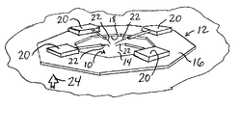
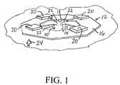
- FIG. 1is a perspective view of an apparatus for probing a semiconductor circuit, where the apparatus is in accordance with an embodiment of the present invention.
- FIG. 2is a block diagram which illustrates a method of probing a semiconductor circuit, where the method is in accordance with an embodiment of the present invention.
- FIG. 1illustrates a wafer 10 and an apparatus 12 for probing a semiconductor circuit 14 on the wafer 10 , where the apparatus 12 is in accordance with an embodiment of the present invention.
- the apparatus 12provides that a semiconductor circuit can be probed using a wafer-mounted micro-probing platform, inexpensively, with no extra spatial requirements.
- the apparatusprovides an in-vacuum chamber probing solution which can be used in a variety of chambers, such as existing SEM/FIB chambers, with little or no retrofitting necessary.
- the platformcan be moved between various inspection/analysis tools without requiring many hours of tool setup time.
- the apparatus 12includes a small platform or platen 16 which is affixed to the surface of a wafer 10 . As shown in FIG. 1 , a hole 18 is preferably provided in the platen 16 , and the hole 18 allows probing of circuitry of interest for several dies in any direction. Probe manipulators 20 are mounted on the platen 16 , generally around the hole 18 , and probes 22 extend from or are otherwise associated with the probe manipulators 20 . The probe manipulators 20 may be fixed in position, or they may be motorized to allow adjustment of the probe positions while in-situ.
- the probe manipulators 20are relatively small, as this provides that the overall height of the platen 16 and probe manipulators 20 can be small, thereby allowing placement of the wafer 10 and platen 16 in various SEM/FIB tools.
- electrical signals(represented by arrow 24 in FIG. 1 ) are preferably sent to the probes 22 viz.-a-viz. feedthrough interfaces, such as feedthrough interfaces which are conventional in presently available SEM/FIB systems.
- the platen 16 which is affixed to the surface of the wafer 10effectively serves two purposes: 1) as a mounting point for the probe manipulators 20 ; and 2) to mechanically stiffen the wafer 10 so that the wafer 10 does not flex, thereby requiring re-positioning of the probes 22 .
- the apparatus 12 shown in FIG. 1i.e., the platen 16 , probe manipulators 20 and probes 22 ) could be used as a stand-alone mechanical probing solution when only several die are intended to be analyzed. While many current probe stations have a footprint or size of several tens of square feet, and require significant facilitation for installation and use, the platen 16 shown in FIG. 1 preferably is small enough to be used on a desktop.
- FIG. 2illustrates a method which is in accordance with an embodiment of the present invention.
- the methodinvolves the installation and use of a wafer-mounted micro-probing platform, such as the apparatus shown in FIG. 1 .
- FIG. 2will be explained with reference to FIG. 1 .
- the methodprovides that the platform or platen 16 is affixed to the wafer 10 , where the platen 16 preferably includes a hole 18 , and carries or has mounted thereon probe manipulators 20 and probes 22 .
- the probes 22are placed in their desired positions, preferably while outside a vacuum chamber, while under a microscope.
- the motorsare actuated to place the probes 22 in their desired positions.
- the wafer 10 and platen 16are loaded into a SEM/FIB chamber, such as into a conventional, existing SEM/FIB chamber.
- electrical signals 24are sent to the probes 22 to conduct probing of the circuitry of interest.
- the platen 16 and wafer 10may be removed from the chamber and the probes 22 re-positioned, under a microscope, to test other dies on the wafer 10 . This process of removing the platen 16 and wafer 10 and re-positioning the probes 22 may be repeated to probe many die on the wafer 10 .
- a method and apparatusare provided for probing semiconductor circuits using a wafer-mounted micro-probing platform, inexpensively, with no extra spatial requirements.
- the method and apparatusprovide an in-vacuum chamber probing solution which can be used in a variety of chambers, such as existing SEM/FIB chambers, with little or no retro-fitting necessary.
- the method and apparatusprovide that the platform can be moved between various inspection/analysis tools without requiring many hours of tool setup time.
Landscapes
- Physics & Mathematics (AREA)
- General Physics & Mathematics (AREA)
- Testing Or Measuring Of Semiconductors Or The Like (AREA)
- Tests Of Electronic Circuits (AREA)
Abstract
Description
Claims (20)
Priority Applications (1)
| Application Number | Priority Date | Filing Date | Title |
|---|---|---|---|
| US10/417,049US7023225B2 (en) | 2003-04-16 | 2003-04-16 | Wafer-mounted micro-probing platform |
Applications Claiming Priority (1)
| Application Number | Priority Date | Filing Date | Title |
|---|---|---|---|
| US10/417,049US7023225B2 (en) | 2003-04-16 | 2003-04-16 | Wafer-mounted micro-probing platform |
Publications (2)
| Publication Number | Publication Date |
|---|---|
| US20040207416A1 US20040207416A1 (en) | 2004-10-21 |
| US7023225B2true US7023225B2 (en) | 2006-04-04 |
Family
ID=33158826
Family Applications (1)
| Application Number | Title | Priority Date | Filing Date |
|---|---|---|---|
| US10/417,049Expired - LifetimeUS7023225B2 (en) | 2003-04-16 | 2003-04-16 | Wafer-mounted micro-probing platform |
Country Status (1)
| Country | Link |
|---|---|
| US (1) | US7023225B2 (en) |
Cited By (52)
| Publication number | Priority date | Publication date | Assignee | Title |
|---|---|---|---|---|
| US20040093716A1 (en)* | 1998-07-14 | 2004-05-20 | Reed Gleason | Membrane probing system |
| US20040207417A1 (en)* | 2003-04-16 | 2004-10-21 | Barr Andrew Harvey | Electronic probe with positionable tip |
| US20050122125A1 (en)* | 2002-12-13 | 2005-06-09 | Cascade Microtech, Inc. | Guarded tub enclosure |
| US20050174133A1 (en)* | 2004-02-11 | 2005-08-11 | Star Technologies Inc. | Probe card |
| US20050194983A1 (en)* | 1992-06-11 | 2005-09-08 | Schwindt Randy J. | Wafer probe station having a skirting component |
| US20060164112A1 (en)* | 1997-06-10 | 2006-07-27 | Cascade Microtech, Inc. | Low-current pogo probe card |
| US20060170439A1 (en)* | 2003-05-23 | 2006-08-03 | Cascade Microtech, Inc. | Probe for testing a device under test |
| US20060202708A1 (en)* | 1995-12-01 | 2006-09-14 | Cascade Microtech, Inc. | Low-current probe card |
| US20060208748A1 (en)* | 1997-05-28 | 2006-09-21 | Cascade Microtech, Inc. | Probe holder for testing of a test device |
| US20060214676A1 (en)* | 1996-08-08 | 2006-09-28 | Cascade Microtech, Inc. | Membrane probing system with local contact scrub |
| US20060229279A1 (en)* | 2002-03-07 | 2006-10-12 | Hartell Mark G | Artemisinins with improved stability and bioavailability for therapeutic drug development and application |
| US20060267610A1 (en)* | 1997-06-06 | 2006-11-30 | Peters Ron A | Probe station having multiple enclosures |
| US20060284630A1 (en)* | 2000-02-25 | 2006-12-21 | Cascade Microtech, Inc. | Membrane probing system |
| US7176705B2 (en) | 2004-06-07 | 2007-02-13 | Cascade Microtech, Inc. | Thermal optical chuck |
| US7178236B2 (en) | 1999-06-04 | 2007-02-20 | Cascade Microtech, Inc. | Method for constructing a membrane probe using a depression |
| US7187188B2 (en) | 2003-12-24 | 2007-03-06 | Cascade Microtech, Inc. | Chuck with integrated wafer support |
| US7205784B2 (en) | 2002-11-13 | 2007-04-17 | Cascade Microtech, Inc. | Probe for combined signals |
| US7221172B2 (en) | 2003-05-06 | 2007-05-22 | Cascade Microtech, Inc. | Switched suspended conductor and connection |
| US7250626B2 (en) | 2003-10-22 | 2007-07-31 | Cascade Microtech, Inc. | Probe testing structure |
| US7250779B2 (en) | 2002-11-25 | 2007-07-31 | Cascade Microtech, Inc. | Probe station with low inductance path |
| US7268533B2 (en) | 2001-08-31 | 2007-09-11 | Cascade Microtech, Inc. | Optical testing device |
| US7292057B2 (en) | 1999-06-30 | 2007-11-06 | Cascade Microtech, Inc. | Probe station thermal chuck with shielding for capacitive current |
| US7295025B2 (en) | 2002-11-08 | 2007-11-13 | Cascade Microtech, Inc. | Probe station with low noise characteristics |
| US20070294047A1 (en)* | 2005-06-11 | 2007-12-20 | Leonard Hayden | Calibration system |
| US7321233B2 (en) | 1995-04-14 | 2008-01-22 | Cascade Microtech, Inc. | System for evaluating probing networks |
| US7330041B2 (en) | 2004-06-14 | 2008-02-12 | Cascade Microtech, Inc. | Localizing a temperature of a device for testing |
| US7348787B2 (en) | 1992-06-11 | 2008-03-25 | Cascade Microtech, Inc. | Wafer probe station having environment control enclosure |
| US7352168B2 (en) | 2000-09-05 | 2008-04-01 | Cascade Microtech, Inc. | Chuck for holding a device under test |
| US7355420B2 (en) | 2001-08-21 | 2008-04-08 | Cascade Microtech, Inc. | Membrane probing system |
| US7368927B2 (en) | 2004-07-07 | 2008-05-06 | Cascade Microtech, Inc. | Probe head having a membrane suspended probe |
| US7368925B2 (en) | 2002-01-25 | 2008-05-06 | Cascade Microtech, Inc. | Probe station with two platens |
| US7403028B2 (en) | 2006-06-12 | 2008-07-22 | Cascade Microtech, Inc. | Test structure and probe for differential signals |
| US7420381B2 (en) | 2004-09-13 | 2008-09-02 | Cascade Microtech, Inc. | Double sided probing structures |
| US7427868B2 (en) | 2003-12-24 | 2008-09-23 | Cascade Microtech, Inc. | Active wafer probe |
| US7436194B2 (en) | 2002-05-23 | 2008-10-14 | Cascade Microtech, Inc. | Shielded probe with low contact resistance for testing a device under test |
| US7443186B2 (en) | 2006-06-12 | 2008-10-28 | Cascade Microtech, Inc. | On-wafer test structures for differential signals |
| US7449899B2 (en) | 2005-06-08 | 2008-11-11 | Cascade Microtech, Inc. | Probe for high frequency signals |
| US7456646B2 (en) | 2000-12-04 | 2008-11-25 | Cascade Microtech, Inc. | Wafer probe |
| US7492172B2 (en) | 2003-05-23 | 2009-02-17 | Cascade Microtech, Inc. | Chuck for holding a device under test |
| US7535247B2 (en) | 2005-01-31 | 2009-05-19 | Cascade Microtech, Inc. | Interface for testing semiconductors |
| US7554322B2 (en) | 2000-09-05 | 2009-06-30 | Cascade Microtech, Inc. | Probe station |
| US7609077B2 (en) | 2006-06-09 | 2009-10-27 | Cascade Microtech, Inc. | Differential signal probe with integral balun |
| US7619419B2 (en) | 2005-06-13 | 2009-11-17 | Cascade Microtech, Inc. | Wideband active-passive differential signal probe |
| US7656172B2 (en) | 2005-01-31 | 2010-02-02 | Cascade Microtech, Inc. | System for testing semiconductors |
| US7723999B2 (en) | 2006-06-12 | 2010-05-25 | Cascade Microtech, Inc. | Calibration structures for differential signal probing |
| US7764072B2 (en) | 2006-06-12 | 2010-07-27 | Cascade Microtech, Inc. | Differential signal probing system |
| US7876114B2 (en) | 2007-08-08 | 2011-01-25 | Cascade Microtech, Inc. | Differential waveguide probe |
| US7888957B2 (en) | 2008-10-06 | 2011-02-15 | Cascade Microtech, Inc. | Probing apparatus with impedance optimized interface |
| US8319503B2 (en) | 2008-11-24 | 2012-11-27 | Cascade Microtech, Inc. | Test apparatus for measuring a characteristic of a device under test |
| US8410806B2 (en) | 2008-11-21 | 2013-04-02 | Cascade Microtech, Inc. | Replaceable coupon for a probing apparatus |
| US9709600B2 (en) | 2013-08-14 | 2017-07-18 | Fei Company | Circuit probe for charged particle beam system |
| US10459006B2 (en) | 2016-09-28 | 2019-10-29 | Formfactor Beaverton, Inc. | Probe systems and methods |
Families Citing this family (1)
| Publication number | Priority date | Publication date | Assignee | Title |
|---|---|---|---|---|
| CN102981114B (en)* | 2012-12-10 | 2015-09-09 | 深圳深爱半导体股份有限公司 | The method of testing of chip in wafer |
Citations (6)
| Publication number | Priority date | Publication date | Assignee | Title |
|---|---|---|---|---|
| US4266191A (en)* | 1979-04-18 | 1981-05-05 | Spano John D | Test probe alignment apparatus |
| US4623839A (en)* | 1982-09-17 | 1986-11-18 | Angliatech Limited | Probe device for testing an integrated circuit |
| US5959461A (en)* | 1997-07-14 | 1999-09-28 | Wentworth Laboratories, Inc. | Probe station adapter for backside emission inspection |
| US6031383A (en)* | 1997-07-15 | 2000-02-29 | Wentworth Laboratories, Inc. | Probe station for low current, low voltage parametric measurements using multiple probes |
| US6198299B1 (en)* | 1998-08-27 | 2001-03-06 | The Micromanipulator Company, Inc. | High Resolution analytical probe station |
| US6605951B1 (en)* | 2000-12-11 | 2003-08-12 | Lsi Logic Corporation | Interconnector and method of connecting probes to a die for functional analysis |
- 2003
- 2003-04-16USUS10/417,049patent/US7023225B2/ennot_activeExpired - Lifetime
Patent Citations (6)
| Publication number | Priority date | Publication date | Assignee | Title |
|---|---|---|---|---|
| US4266191A (en)* | 1979-04-18 | 1981-05-05 | Spano John D | Test probe alignment apparatus |
| US4623839A (en)* | 1982-09-17 | 1986-11-18 | Angliatech Limited | Probe device for testing an integrated circuit |
| US5959461A (en)* | 1997-07-14 | 1999-09-28 | Wentworth Laboratories, Inc. | Probe station adapter for backside emission inspection |
| US6031383A (en)* | 1997-07-15 | 2000-02-29 | Wentworth Laboratories, Inc. | Probe station for low current, low voltage parametric measurements using multiple probes |
| US6198299B1 (en)* | 1998-08-27 | 2001-03-06 | The Micromanipulator Company, Inc. | High Resolution analytical probe station |
| US6605951B1 (en)* | 2000-12-11 | 2003-08-12 | Lsi Logic Corporation | Interconnector and method of connecting probes to a die for functional analysis |
Cited By (115)
| Publication number | Priority date | Publication date | Assignee | Title |
|---|---|---|---|---|
| US7595632B2 (en) | 1992-06-11 | 2009-09-29 | Cascade Microtech, Inc. | Wafer probe station having environment control enclosure |
| US7492147B2 (en) | 1992-06-11 | 2009-02-17 | Cascade Microtech, Inc. | Wafer probe station having a skirting component |
| US7348787B2 (en) | 1992-06-11 | 2008-03-25 | Cascade Microtech, Inc. | Wafer probe station having environment control enclosure |
| US20050194983A1 (en)* | 1992-06-11 | 2005-09-08 | Schwindt Randy J. | Wafer probe station having a skirting component |
| US7330023B2 (en) | 1992-06-11 | 2008-02-12 | Cascade Microtech, Inc. | Wafer probe station having a skirting component |
| US7589518B2 (en) | 1992-06-11 | 2009-09-15 | Cascade Microtech, Inc. | Wafer probe station having a skirting component |
| US7321233B2 (en) | 1995-04-14 | 2008-01-22 | Cascade Microtech, Inc. | System for evaluating probing networks |
| US20060202708A1 (en)* | 1995-12-01 | 2006-09-14 | Cascade Microtech, Inc. | Low-current probe card |
| US20060214676A1 (en)* | 1996-08-08 | 2006-09-28 | Cascade Microtech, Inc. | Membrane probing system with local contact scrub |
| US7550983B2 (en) | 1996-08-08 | 2009-06-23 | Cascade Microtech, Inc. | Membrane probing system with local contact scrub |
| US7541821B2 (en) | 1996-08-08 | 2009-06-02 | Cascade Microtech, Inc. | Membrane probing system with local contact scrub |
| US7893704B2 (en) | 1996-08-08 | 2011-02-22 | Cascade Microtech, Inc. | Membrane probing structure with laterally scrubbing contacts |
| US20070296431A1 (en)* | 1996-08-08 | 2007-12-27 | Cascade Microtech, Inc. | Membrane probing system with local contact scrub |
| US20060208748A1 (en)* | 1997-05-28 | 2006-09-21 | Cascade Microtech, Inc. | Probe holder for testing of a test device |
| US7504842B2 (en) | 1997-05-28 | 2009-03-17 | Cascade Microtech, Inc. | Probe holder for testing of a test device |
| US7221174B2 (en) | 1997-05-28 | 2007-05-22 | Cascade Microtech, Inc. | Probe holder for testing of a test device |
| US7250752B2 (en) | 1997-06-06 | 2007-07-31 | Cascade Microtech, Inc. | Probe station having multiple enclosures |
| US20060267610A1 (en)* | 1997-06-06 | 2006-11-30 | Peters Ron A | Probe station having multiple enclosures |
| US7436170B2 (en) | 1997-06-06 | 2008-10-14 | Cascade Microtech, Inc. | Probe station having multiple enclosures |
| US7626379B2 (en) | 1997-06-06 | 2009-12-01 | Cascade Microtech, Inc. | Probe station having multiple enclosures |
| US20060164112A1 (en)* | 1997-06-10 | 2006-07-27 | Cascade Microtech, Inc. | Low-current pogo probe card |
| US7400155B2 (en) | 1998-07-14 | 2008-07-15 | Cascade Microtech, Inc. | Membrane probing system |
| US7761986B2 (en) | 1998-07-14 | 2010-07-27 | Cascade Microtech, Inc. | Membrane probing method using improved contact |
| US7681312B2 (en) | 1998-07-14 | 2010-03-23 | Cascade Microtech, Inc. | Membrane probing system |
| US7266889B2 (en) | 1998-07-14 | 2007-09-11 | Cascade Microtech, Inc. | Membrane probing system |
| US20040093716A1 (en)* | 1998-07-14 | 2004-05-20 | Reed Gleason | Membrane probing system |
| US8451017B2 (en) | 1998-07-14 | 2013-05-28 | Cascade Microtech, Inc. | Membrane probing method using improved contact |
| US20070074392A1 (en)* | 1999-06-04 | 2007-04-05 | Cascade Microtech, Inc. | Membrane probing system |
| US7178236B2 (en) | 1999-06-04 | 2007-02-20 | Cascade Microtech, Inc. | Method for constructing a membrane probe using a depression |
| US7533462B2 (en) | 1999-06-04 | 2009-05-19 | Cascade Microtech, Inc. | Method of constructing a membrane probe |
| US7292057B2 (en) | 1999-06-30 | 2007-11-06 | Cascade Microtech, Inc. | Probe station thermal chuck with shielding for capacitive current |
| US7616017B2 (en) | 1999-06-30 | 2009-11-10 | Cascade Microtech, Inc. | Probe station thermal chuck with shielding for capacitive current |
| US7403025B2 (en) | 2000-02-25 | 2008-07-22 | Cascade Microtech, Inc. | Membrane probing system |
| US20060284630A1 (en)* | 2000-02-25 | 2006-12-21 | Cascade Microtech, Inc. | Membrane probing system |
| US7352168B2 (en) | 2000-09-05 | 2008-04-01 | Cascade Microtech, Inc. | Chuck for holding a device under test |
| US7969173B2 (en) | 2000-09-05 | 2011-06-28 | Cascade Microtech, Inc. | Chuck for holding a device under test |
| US7554322B2 (en) | 2000-09-05 | 2009-06-30 | Cascade Microtech, Inc. | Probe station |
| US7423419B2 (en) | 2000-09-05 | 2008-09-09 | Cascade Microtech, Inc. | Chuck for holding a device under test |
| US7514915B2 (en) | 2000-09-05 | 2009-04-07 | Cascade Microtech, Inc. | Chuck for holding a device under test |
| US7501810B2 (en) | 2000-09-05 | 2009-03-10 | Cascade Microtech, Inc. | Chuck for holding a device under test |
| US7688062B2 (en) | 2000-09-05 | 2010-03-30 | Cascade Microtech, Inc. | Probe station |
| US7518358B2 (en) | 2000-09-05 | 2009-04-14 | Cascade Microtech, Inc. | Chuck for holding a device under test |
| US7688097B2 (en) | 2000-12-04 | 2010-03-30 | Cascade Microtech, Inc. | Wafer probe |
| US7456646B2 (en) | 2000-12-04 | 2008-11-25 | Cascade Microtech, Inc. | Wafer probe |
| US7495461B2 (en) | 2000-12-04 | 2009-02-24 | Cascade Microtech, Inc. | Wafer probe |
| US7761983B2 (en) | 2000-12-04 | 2010-07-27 | Cascade Microtech, Inc. | Method of assembling a wafer probe |
| US20080111571A1 (en)* | 2001-08-21 | 2008-05-15 | Cascade Microtech, Inc. | Membrane probing system |
| US7355420B2 (en) | 2001-08-21 | 2008-04-08 | Cascade Microtech, Inc. | Membrane probing system |
| US7492175B2 (en) | 2001-08-21 | 2009-02-17 | Cascade Microtech, Inc. | Membrane probing system |
| US7268533B2 (en) | 2001-08-31 | 2007-09-11 | Cascade Microtech, Inc. | Optical testing device |
| US7368925B2 (en) | 2002-01-25 | 2008-05-06 | Cascade Microtech, Inc. | Probe station with two platens |
| US20060229279A1 (en)* | 2002-03-07 | 2006-10-12 | Hartell Mark G | Artemisinins with improved stability and bioavailability for therapeutic drug development and application |
| US7436194B2 (en) | 2002-05-23 | 2008-10-14 | Cascade Microtech, Inc. | Shielded probe with low contact resistance for testing a device under test |
| US7518387B2 (en) | 2002-05-23 | 2009-04-14 | Cascade Microtech, Inc. | Shielded probe for testing a device under test |
| US7489149B2 (en) | 2002-05-23 | 2009-02-10 | Cascade Microtech, Inc. | Shielded probe for testing a device under test |
| US7482823B2 (en) | 2002-05-23 | 2009-01-27 | Cascade Microtech, Inc. | Shielded probe for testing a device under test |
| US7295025B2 (en) | 2002-11-08 | 2007-11-13 | Cascade Microtech, Inc. | Probe station with low noise characteristics |
| US7550984B2 (en) | 2002-11-08 | 2009-06-23 | Cascade Microtech, Inc. | Probe station with low noise characteristics |
| US7285969B2 (en) | 2002-11-13 | 2007-10-23 | Cascade Microtech, Inc. | Probe for combined signals |
| US7417446B2 (en) | 2002-11-13 | 2008-08-26 | Cascade Microtech, Inc. | Probe for combined signals |
| US7453276B2 (en) | 2002-11-13 | 2008-11-18 | Cascade Microtech, Inc. | Probe for combined signals |
| US7205784B2 (en) | 2002-11-13 | 2007-04-17 | Cascade Microtech, Inc. | Probe for combined signals |
| US7498828B2 (en) | 2002-11-25 | 2009-03-03 | Cascade Microtech, Inc. | Probe station with low inductance path |
| US7250779B2 (en) | 2002-11-25 | 2007-07-31 | Cascade Microtech, Inc. | Probe station with low inductance path |
| US7221146B2 (en) | 2002-12-13 | 2007-05-22 | Cascade Microtech, Inc. | Guarded tub enclosure |
| US7639003B2 (en) | 2002-12-13 | 2009-12-29 | Cascade Microtech, Inc. | Guarded tub enclosure |
| US20050122125A1 (en)* | 2002-12-13 | 2005-06-09 | Cascade Microtech, Inc. | Guarded tub enclosure |
| US20040207417A1 (en)* | 2003-04-16 | 2004-10-21 | Barr Andrew Harvey | Electronic probe with positionable tip |
| US7468609B2 (en) | 2003-05-06 | 2008-12-23 | Cascade Microtech, Inc. | Switched suspended conductor and connection |
| US7221172B2 (en) | 2003-05-06 | 2007-05-22 | Cascade Microtech, Inc. | Switched suspended conductor and connection |
| US7898273B2 (en) | 2003-05-23 | 2011-03-01 | Cascade Microtech, Inc. | Probe for testing a device under test |
| US7271603B2 (en) | 2003-05-23 | 2007-09-18 | Cascade Microtech, Inc. | Shielded probe for testing a device under test |
| US7876115B2 (en) | 2003-05-23 | 2011-01-25 | Cascade Microtech, Inc. | Chuck for holding a device under test |
| US20060170439A1 (en)* | 2003-05-23 | 2006-08-03 | Cascade Microtech, Inc. | Probe for testing a device under test |
| US7501842B2 (en) | 2003-05-23 | 2009-03-10 | Cascade Microtech, Inc. | Shielded probe for testing a device under test |
| US7498829B2 (en) | 2003-05-23 | 2009-03-03 | Cascade Microtech, Inc. | Shielded probe for testing a device under test |
| US7492172B2 (en) | 2003-05-23 | 2009-02-17 | Cascade Microtech, Inc. | Chuck for holding a device under test |
| US8069491B2 (en) | 2003-10-22 | 2011-11-29 | Cascade Microtech, Inc. | Probe testing structure |
| US7250626B2 (en) | 2003-10-22 | 2007-07-31 | Cascade Microtech, Inc. | Probe testing structure |
| US7688091B2 (en) | 2003-12-24 | 2010-03-30 | Cascade Microtech, Inc. | Chuck with integrated wafer support |
| US7187188B2 (en) | 2003-12-24 | 2007-03-06 | Cascade Microtech, Inc. | Chuck with integrated wafer support |
| US7362115B2 (en) | 2003-12-24 | 2008-04-22 | Cascade Microtech, Inc. | Chuck with integrated wafer support |
| US7759953B2 (en) | 2003-12-24 | 2010-07-20 | Cascade Microtech, Inc. | Active wafer probe |
| US7427868B2 (en) | 2003-12-24 | 2008-09-23 | Cascade Microtech, Inc. | Active wafer probe |
| US20050174133A1 (en)* | 2004-02-11 | 2005-08-11 | Star Technologies Inc. | Probe card |
| US7253646B2 (en)* | 2004-02-11 | 2007-08-07 | Star Technologies Inc. | Probe card with tunable stage and at least one replaceable probe |
| US7504823B2 (en) | 2004-06-07 | 2009-03-17 | Cascade Microtech, Inc. | Thermal optical chuck |
| US7176705B2 (en) | 2004-06-07 | 2007-02-13 | Cascade Microtech, Inc. | Thermal optical chuck |
| US7330041B2 (en) | 2004-06-14 | 2008-02-12 | Cascade Microtech, Inc. | Localizing a temperature of a device for testing |
| US7368927B2 (en) | 2004-07-07 | 2008-05-06 | Cascade Microtech, Inc. | Probe head having a membrane suspended probe |
| US7514944B2 (en) | 2004-07-07 | 2009-04-07 | Cascade Microtech, Inc. | Probe head having a membrane suspended probe |
| US7420381B2 (en) | 2004-09-13 | 2008-09-02 | Cascade Microtech, Inc. | Double sided probing structures |
| US8013623B2 (en) | 2004-09-13 | 2011-09-06 | Cascade Microtech, Inc. | Double sided probing structures |
| US7535247B2 (en) | 2005-01-31 | 2009-05-19 | Cascade Microtech, Inc. | Interface for testing semiconductors |
| US7656172B2 (en) | 2005-01-31 | 2010-02-02 | Cascade Microtech, Inc. | System for testing semiconductors |
| US7940069B2 (en) | 2005-01-31 | 2011-05-10 | Cascade Microtech, Inc. | System for testing semiconductors |
| US7898281B2 (en) | 2005-01-31 | 2011-03-01 | Cascade Mircotech, Inc. | Interface for testing semiconductors |
| US7449899B2 (en) | 2005-06-08 | 2008-11-11 | Cascade Microtech, Inc. | Probe for high frequency signals |
| US20070294047A1 (en)* | 2005-06-11 | 2007-12-20 | Leonard Hayden | Calibration system |
| US7619419B2 (en) | 2005-06-13 | 2009-11-17 | Cascade Microtech, Inc. | Wideband active-passive differential signal probe |
| US7609077B2 (en) | 2006-06-09 | 2009-10-27 | Cascade Microtech, Inc. | Differential signal probe with integral balun |
| US7443186B2 (en) | 2006-06-12 | 2008-10-28 | Cascade Microtech, Inc. | On-wafer test structures for differential signals |
| US7403028B2 (en) | 2006-06-12 | 2008-07-22 | Cascade Microtech, Inc. | Test structure and probe for differential signals |
| US7764072B2 (en) | 2006-06-12 | 2010-07-27 | Cascade Microtech, Inc. | Differential signal probing system |
| US7750652B2 (en) | 2006-06-12 | 2010-07-06 | Cascade Microtech, Inc. | Test structure and probe for differential signals |
| US7723999B2 (en) | 2006-06-12 | 2010-05-25 | Cascade Microtech, Inc. | Calibration structures for differential signal probing |
| US7876114B2 (en) | 2007-08-08 | 2011-01-25 | Cascade Microtech, Inc. | Differential waveguide probe |
| US7888957B2 (en) | 2008-10-06 | 2011-02-15 | Cascade Microtech, Inc. | Probing apparatus with impedance optimized interface |
| US8410806B2 (en) | 2008-11-21 | 2013-04-02 | Cascade Microtech, Inc. | Replaceable coupon for a probing apparatus |
| US9429638B2 (en) | 2008-11-21 | 2016-08-30 | Cascade Microtech, Inc. | Method of replacing an existing contact of a wafer probing assembly |
| US10267848B2 (en) | 2008-11-21 | 2019-04-23 | Formfactor Beaverton, Inc. | Method of electrically contacting a bond pad of a device under test with a probe |
| US8319503B2 (en) | 2008-11-24 | 2012-11-27 | Cascade Microtech, Inc. | Test apparatus for measuring a characteristic of a device under test |
| US9709600B2 (en) | 2013-08-14 | 2017-07-18 | Fei Company | Circuit probe for charged particle beam system |
| US10459006B2 (en) | 2016-09-28 | 2019-10-29 | Formfactor Beaverton, Inc. | Probe systems and methods |
| US11047879B2 (en) | 2016-09-28 | 2021-06-29 | Formfactor, Inc. | Probe systems and methods |
Also Published As
| Publication number | Publication date |
|---|---|
| US20040207416A1 (en) | 2004-10-21 |
Similar Documents
| Publication | Publication Date | Title |
|---|---|---|
| US7023225B2 (en) | Wafer-mounted micro-probing platform | |
| US7211997B2 (en) | Planarity diagnostic system, E.G., for microelectronic component test systems | |
| KR101331353B1 (en) | Method and apparatus for cleaning a probe card | |
| WO2008144437A1 (en) | Wafer probe test and inspection system | |
| US11594435B2 (en) | Apparatus and methods for testing semiconductor devices | |
| US7692433B2 (en) | Sawing tile corners on probe card substrates | |
| US7265536B2 (en) | Procedure for reproduction of a calibration position of an aligned and afterwards displaced calibration substrate in a probe station | |
| JPH1126525A (en) | Probe tile and platform for detailed inspection of wafer having large area | |
| US7841071B2 (en) | Position-correction device for correcting the position of a component holder for electronic components | |
| US6310486B1 (en) | Integrated test cell | |
| JPH08335614A (en) | Probe system | |
| US20200225282A1 (en) | Chuck top, inspection apparatus, and chuck top recovery method | |
| US7196507B2 (en) | Apparatus for testing substrates | |
| CN115993470A (en) | Inspection apparatus and inspection method | |
| US7131209B2 (en) | Apparatus for measuring horizontal level of a wafer chuck | |
| KR102413745B1 (en) | Electrical connecting device, inspection apparatus, and method for electrical connection between contact target and contact member | |
| JP2008117897A (en) | Prober and probing inspection method | |
| US5675261A (en) | Probe card locking device of a probe station for testing a semiconductor wafer | |
| KR960007507B1 (en) | IC test equipment | |
| US20240131730A1 (en) | Magnetically retained replaceable cylinder component for pick-and-place test head unit | |
| JP2000049200A (en) | Prober | |
| JPH10229107A (en) | Semiconductor analysis device | |
| JP2533178B2 (en) | Tester head mounted stand | |
| JPH06274215A (en) | Work inspection device | |
| US20050174139A1 (en) | Apparatus for high speed probing of flat panel displays |
Legal Events
| Date | Code | Title | Description |
|---|---|---|---|
| AS | Assignment | Owner name:LSI LOGIC CORPORATION, CALIFORNIA Free format text:ASSIGNMENT OF ASSIGNORS INTEREST;ASSIGNOR:BLACKWOOD, JEFFREY;REEL/FRAME:013978/0364 Effective date:20030414 | |
| STCF | Information on status: patent grant | Free format text:PATENTED CASE | |
| FEPP | Fee payment procedure | Free format text:PAYOR NUMBER ASSIGNED (ORIGINAL EVENT CODE: ASPN); ENTITY STATUS OF PATENT OWNER: LARGE ENTITY | |
| FPAY | Fee payment | Year of fee payment:4 | |
| FPAY | Fee payment | Year of fee payment:8 | |
| AS | Assignment | Owner name:DEUTSCHE BANK AG NEW YORK BRANCH, AS COLLATERAL AG Free format text:PATENT SECURITY AGREEMENT;ASSIGNORS:LSI CORPORATION;AGERE SYSTEMS LLC;REEL/FRAME:032856/0031 Effective date:20140506 | |
| AS | Assignment | Owner name:LSI CORPORATION, CALIFORNIA Free format text:CHANGE OF NAME;ASSIGNOR:LSI LOGIC CORPORATION;REEL/FRAME:033102/0270 Effective date:20070406 | |
| AS | Assignment | Owner name:AVAGO TECHNOLOGIES GENERAL IP (SINGAPORE) PTE. LTD Free format text:ASSIGNMENT OF ASSIGNORS INTEREST;ASSIGNOR:LSI CORPORATION;REEL/FRAME:035390/0388 Effective date:20140814 | |
| AS | Assignment | Owner name:LSI CORPORATION, CALIFORNIA Free format text:TERMINATION AND RELEASE OF SECURITY INTEREST IN PATENT RIGHTS (RELEASES RF 032856-0031);ASSIGNOR:DEUTSCHE BANK AG NEW YORK BRANCH, AS COLLATERAL AGENT;REEL/FRAME:037684/0039 Effective date:20160201 Owner name:AGERE SYSTEMS LLC, PENNSYLVANIA Free format text:TERMINATION AND RELEASE OF SECURITY INTEREST IN PATENT RIGHTS (RELEASES RF 032856-0031);ASSIGNOR:DEUTSCHE BANK AG NEW YORK BRANCH, AS COLLATERAL AGENT;REEL/FRAME:037684/0039 Effective date:20160201 | |
| AS | Assignment | Owner name:BANK OF AMERICA, N.A., AS COLLATERAL AGENT, NORTH CAROLINA Free format text:PATENT SECURITY AGREEMENT;ASSIGNOR:AVAGO TECHNOLOGIES GENERAL IP (SINGAPORE) PTE. LTD.;REEL/FRAME:037808/0001 Effective date:20160201 Owner name:BANK OF AMERICA, N.A., AS COLLATERAL AGENT, NORTH Free format text:PATENT SECURITY AGREEMENT;ASSIGNOR:AVAGO TECHNOLOGIES GENERAL IP (SINGAPORE) PTE. LTD.;REEL/FRAME:037808/0001 Effective date:20160201 | |
| AS | Assignment | Owner name:AVAGO TECHNOLOGIES GENERAL IP (SINGAPORE) PTE. LTD., SINGAPORE Free format text:TERMINATION AND RELEASE OF SECURITY INTEREST IN PATENTS;ASSIGNOR:BANK OF AMERICA, N.A., AS COLLATERAL AGENT;REEL/FRAME:041710/0001 Effective date:20170119 Owner name:AVAGO TECHNOLOGIES GENERAL IP (SINGAPORE) PTE. LTD Free format text:TERMINATION AND RELEASE OF SECURITY INTEREST IN PATENTS;ASSIGNOR:BANK OF AMERICA, N.A., AS COLLATERAL AGENT;REEL/FRAME:041710/0001 Effective date:20170119 | |
| MAFP | Maintenance fee payment | Free format text:PAYMENT OF MAINTENANCE FEE, 12TH YEAR, LARGE ENTITY (ORIGINAL EVENT CODE: M1553) Year of fee payment:12 | |
| AS | Assignment | Owner name:BELL SEMICONDUCTOR, LLC, ILLINOIS Free format text:ASSIGNMENT OF ASSIGNORS INTEREST;ASSIGNORS:AVAGO TECHNOLOGIES GENERAL IP (SINGAPORE) PTE. LTD.;BROADCOM CORPORATION;REEL/FRAME:044886/0766 Effective date:20171208 | |
| AS | Assignment | Owner name:CORTLAND CAPITAL MARKET SERVICES LLC, AS COLLATERA Free format text:SECURITY INTEREST;ASSIGNORS:HILCO PATENT ACQUISITION 56, LLC;BELL SEMICONDUCTOR, LLC;BELL NORTHERN RESEARCH, LLC;REEL/FRAME:045216/0020 Effective date:20180124 | |
| AS | Assignment | Owner name:BELL NORTHERN RESEARCH, LLC, ILLINOIS Free format text:RELEASE BY SECURED PARTY;ASSIGNOR:CORTLAND CAPITAL MARKET SERVICES LLC;REEL/FRAME:059723/0382 Effective date:20220401 Owner name:BELL SEMICONDUCTOR, LLC, ILLINOIS Free format text:RELEASE BY SECURED PARTY;ASSIGNOR:CORTLAND CAPITAL MARKET SERVICES LLC;REEL/FRAME:059723/0382 Effective date:20220401 Owner name:HILCO PATENT ACQUISITION 56, LLC, ILLINOIS Free format text:RELEASE BY SECURED PARTY;ASSIGNOR:CORTLAND CAPITAL MARKET SERVICES LLC;REEL/FRAME:059723/0382 Effective date:20220401 |