US7023057B2 - CMOS on hybrid substrate with different crystal orientations using silicon-to-silicon direct wafer bonding - Google Patents
CMOS on hybrid substrate with different crystal orientations using silicon-to-silicon direct wafer bondingDownload PDFInfo
- Publication number
- US7023057B2 US7023057B2US10/799,380US79938004AUS7023057B2US 7023057 B2US7023057 B2US 7023057B2US 79938004 AUS79938004 AUS 79938004AUS 7023057 B2US7023057 B2US 7023057B2
- Authority
- US
- United States
- Prior art keywords
- semiconductor
- semiconductor layer
- layer
- crystallographic orientation
- semiconductor material
- Prior art date
- Legal status (The legal status is an assumption and is not a legal conclusion. Google has not performed a legal analysis and makes no representation as to the accuracy of the status listed.)
- Expired - Lifetime, expires
Links
- 239000000758substrateSubstances0.000titleclaimsabstractdescription60
- 239000013078crystalSubstances0.000titleclaimsdescription23
- 229910052710siliconInorganic materials0.000titleclaimsdescription11
- 239000010703siliconSubstances0.000titledescription9
- 239000004065semiconductorSubstances0.000claimsabstractdescription280
- 239000000463materialSubstances0.000claimsdescription59
- 238000002955isolationMethods0.000claimsdescription16
- 229910000577Silicon-germaniumInorganic materials0.000claimsdescription12
- 229910003811SiGeCInorganic materials0.000claimsdescription4
- 229910003465moissaniteInorganic materials0.000claimsdescription4
- 229910010271silicon carbideInorganic materials0.000claimsdescription4
- 229910001218Gallium arsenideInorganic materials0.000claimsdescription3
- 229910000673Indium arsenideInorganic materials0.000claimsdescription3
- 150000001875compoundsChemical class0.000claimsdescription3
- RPQDHPTXJYYUPQ-UHFFFAOYSA-Nindium arsenideChemical compound[In]#[As]RPQDHPTXJYYUPQ-UHFFFAOYSA-N0.000claimsdescription3
- 238000000034methodMethods0.000abstractdescription45
- 235000012431wafersNutrition0.000description68
- 150000004767nitridesChemical class0.000description18
- 238000005530etchingMethods0.000description17
- 125000006850spacer groupChemical group0.000description16
- 238000000137annealingMethods0.000description12
- 230000015572biosynthetic processEffects0.000description11
- 230000037230mobilityEffects0.000description11
- 239000007943implantSubstances0.000description10
- 239000012212insulatorSubstances0.000description9
- 238000012545processingMethods0.000description9
- XUIMIQQOPSSXEZ-UHFFFAOYSA-NSiliconChemical compound[Si]XUIMIQQOPSSXEZ-UHFFFAOYSA-N0.000description7
- 238000013459approachMethods0.000description7
- 238000012546transferMethods0.000description7
- 238000000407epitaxyMethods0.000description6
- 238000010438heat treatmentMethods0.000description5
- 150000002500ionsChemical class0.000description5
- 238000001020plasma etchingMethods0.000description5
- 230000005660hydrophilic surfaceEffects0.000description4
- 239000000203mixtureSubstances0.000description4
- 229910052786argonInorganic materials0.000description3
- 239000004020conductorSubstances0.000description3
- 238000005516engineering processMethods0.000description3
- 230000005661hydrophobic surfaceEffects0.000description3
- 239000011261inert gasSubstances0.000description3
- 238000001459lithographyMethods0.000description3
- 239000000126substanceSubstances0.000description3
- 238000001039wet etchingMethods0.000description3
- XKRFYHLGVUSROY-UHFFFAOYSA-NArgonChemical compound[Ar]XKRFYHLGVUSROY-UHFFFAOYSA-N0.000description2
- 239000012298atmosphereSubstances0.000description2
- 238000005229chemical vapour depositionMethods0.000description2
- 238000000151depositionMethods0.000description2
- 230000008021depositionEffects0.000description2
- 238000013461designMethods0.000description2
- 238000009792diffusion processMethods0.000description2
- 239000002019doping agentSubstances0.000description2
- 238000001312dry etchingMethods0.000description2
- 230000000694effectsEffects0.000description2
- 239000001257hydrogenSubstances0.000description2
- 229910052739hydrogenInorganic materials0.000description2
- 238000005468ion implantationMethods0.000description2
- 238000004519manufacturing processMethods0.000description2
- 230000003647oxidationEffects0.000description2
- 238000007254oxidation reactionMethods0.000description2
- 238000000623plasma-assisted chemical vapour depositionMethods0.000description2
- 238000004381surface treatmentMethods0.000description2
- UFHFLCQGNIYNRP-UHFFFAOYSA-NHydrogenChemical compound[H][H]UFHFLCQGNIYNRP-UHFFFAOYSA-N0.000description1
- GRYLNZFGIOXLOG-UHFFFAOYSA-NNitric acidChemical compoundO[N+]([O-])=OGRYLNZFGIOXLOG-UHFFFAOYSA-N0.000description1
- QAOWNCQODCNURD-UHFFFAOYSA-NSulfuric acidChemical compoundOS(O)(=O)=OQAOWNCQODCNURD-UHFFFAOYSA-N0.000description1
- 239000002253acidSubstances0.000description1
- 239000000853adhesiveSubstances0.000description1
- 230000001070adhesive effectEffects0.000description1
- 229910045601alloyInorganic materials0.000description1
- 239000000956alloySubstances0.000description1
- 229910021417amorphous siliconInorganic materials0.000description1
- 238000000231atomic layer depositionMethods0.000description1
- QVGXLLKOCUKJST-UHFFFAOYSA-Natomic oxygenChemical compound[O]QVGXLLKOCUKJST-UHFFFAOYSA-N0.000description1
- 230000004888barrier functionEffects0.000description1
- 238000000224chemical solution depositionMethods0.000description1
- 239000003795chemical substances by applicationSubstances0.000description1
- 230000007547defectEffects0.000description1
- 238000000280densificationMethods0.000description1
- 238000005137deposition processMethods0.000description1
- 239000003989dielectric materialSubstances0.000description1
- 230000005669field effectEffects0.000description1
- 238000011049fillingMethods0.000description1
- 238000000227grindingMethods0.000description1
- -1hydrogen ionsChemical class0.000description1
- 230000002209hydrophobic effectEffects0.000description1
- 239000011810insulating materialSubstances0.000description1
- 238000010884ion-beam techniqueMethods0.000description1
- 238000010329laser etchingMethods0.000description1
- 230000000873masking effectEffects0.000description1
- 229910044991metal oxideInorganic materials0.000description1
- 150000004706metal oxidesChemical class0.000description1
- 229910017604nitric acidInorganic materials0.000description1
- 230000001590oxidative effectEffects0.000description1
- 239000001301oxygenSubstances0.000description1
- 229910052760oxygenInorganic materials0.000description1
- 230000003071parasitic effectEffects0.000description1
- 238000000059patterningMethods0.000description1
- 238000005240physical vapour depositionMethods0.000description1
- 238000005498polishingMethods0.000description1
- 229910021420polycrystalline siliconInorganic materials0.000description1
- 229920005591polysiliconPolymers0.000description1
Images


Classifications
- H—ELECTRICITY
- H01—ELECTRIC ELEMENTS
- H01L—SEMICONDUCTOR DEVICES NOT COVERED BY CLASS H10
- H01L21/00—Processes or apparatus adapted for the manufacture or treatment of semiconductor or solid state devices or of parts thereof
- H01L21/70—Manufacture or treatment of devices consisting of a plurality of solid state components formed in or on a common substrate or of parts thereof; Manufacture of integrated circuit devices or of parts thereof
- H01L21/71—Manufacture of specific parts of devices defined in group H01L21/70
- H01L21/76—Making of isolation regions between components
- H01L21/762—Dielectric regions, e.g. EPIC dielectric isolation, LOCOS; Trench refilling techniques, SOI technology, use of channel stoppers
- H01L21/7624—Dielectric regions, e.g. EPIC dielectric isolation, LOCOS; Trench refilling techniques, SOI technology, use of channel stoppers using semiconductor on insulator [SOI] technology
- H01L21/76251—Dielectric regions, e.g. EPIC dielectric isolation, LOCOS; Trench refilling techniques, SOI technology, use of channel stoppers using semiconductor on insulator [SOI] technology using bonding techniques
- H01L21/76254—Dielectric regions, e.g. EPIC dielectric isolation, LOCOS; Trench refilling techniques, SOI technology, use of channel stoppers using semiconductor on insulator [SOI] technology using bonding techniques with separation/delamination along an ion implanted layer, e.g. Smart-cut, Unibond
- H—ELECTRICITY
- H10—SEMICONDUCTOR DEVICES; ELECTRIC SOLID-STATE DEVICES NOT OTHERWISE PROVIDED FOR
- H10D—INORGANIC ELECTRIC SEMICONDUCTOR DEVICES
- H10D84/00—Integrated devices formed in or on semiconductor substrates that comprise only semiconducting layers, e.g. on Si wafers or on GaAs-on-Si wafers
- H10D84/01—Manufacture or treatment
- H10D84/0123—Integrating together multiple components covered by H10D12/00 or H10D30/00, e.g. integrating multiple IGBTs
- H10D84/0126—Integrating together multiple components covered by H10D12/00 or H10D30/00, e.g. integrating multiple IGBTs the components including insulated gates, e.g. IGFETs
- H10D84/0165—Integrating together multiple components covered by H10D12/00 or H10D30/00, e.g. integrating multiple IGBTs the components including insulated gates, e.g. IGFETs the components including complementary IGFETs, e.g. CMOS devices
- H10D84/0167—Manufacturing their channels
- H—ELECTRICITY
- H10—SEMICONDUCTOR DEVICES; ELECTRIC SOLID-STATE DEVICES NOT OTHERWISE PROVIDED FOR
- H10D—INORGANIC ELECTRIC SEMICONDUCTOR DEVICES
- H10D84/00—Integrated devices formed in or on semiconductor substrates that comprise only semiconducting layers, e.g. on Si wafers or on GaAs-on-Si wafers
- H10D84/01—Manufacture or treatment
- H10D84/0123—Integrating together multiple components covered by H10D12/00 or H10D30/00, e.g. integrating multiple IGBTs
- H10D84/0126—Integrating together multiple components covered by H10D12/00 or H10D30/00, e.g. integrating multiple IGBTs the components including insulated gates, e.g. IGFETs
- H10D84/0165—Integrating together multiple components covered by H10D12/00 or H10D30/00, e.g. integrating multiple IGBTs the components including insulated gates, e.g. IGFETs the components including complementary IGFETs, e.g. CMOS devices
- H10D84/0188—Manufacturing their isolation regions
- H—ELECTRICITY
- H10—SEMICONDUCTOR DEVICES; ELECTRIC SOLID-STATE DEVICES NOT OTHERWISE PROVIDED FOR
- H10D—INORGANIC ELECTRIC SEMICONDUCTOR DEVICES
- H10D84/00—Integrated devices formed in or on semiconductor substrates that comprise only semiconducting layers, e.g. on Si wafers or on GaAs-on-Si wafers
- H10D84/01—Manufacture or treatment
- H10D84/02—Manufacture or treatment characterised by using material-based technologies
- H10D84/03—Manufacture or treatment characterised by using material-based technologies using Group IV technology, e.g. silicon technology or silicon-carbide [SiC] technology
- H10D84/038—Manufacture or treatment characterised by using material-based technologies using Group IV technology, e.g. silicon technology or silicon-carbide [SiC] technology using silicon technology, e.g. SiGe
Definitions
- CMOS devicessuch as nFETs or pFETs
- semiconductor waferssuch as Si
- Sisemiconductor wafers
- most of today's semiconductor devicesare built upon Si having a (100) crystal orientation.
- One object of the present inventionis to provide a method of integrating semiconductor devices such that different types of devices are formed upon a specific crystal orientation of a hybrid substrate that enhances the performance of each type of device.
- Another aspect of the present inventionis directed to a method of fabricating the aforementioned hybrid substrate.
- the hybrid substrateis fabricated using a method that comprises:
- first semiconductor wafercomprising a first semiconductor material having a first crystallographic orientation and a second semiconductor wafer comprising a second semiconductor material having a second crystallographic orientation which is different from the first crystallographic orientation;
- a hybrid substratecomprising at least a first semiconductor layer of a first crystallographic orientation and a second semiconductor layer of a second crystallographic orientation separated by an interface (conductive or insulating), said first crystallographic orientation is different from said second crystallographic orientation and said first semiconductor layer lies below said second semiconductor layer;
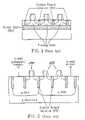
- FIG. 2is a pictorial representation (through a cross sectional view) illustrating a prior art structure including MOSFETs on a bulk substrate in which well contacts are present.
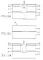
- FIGS. 5A–5Eare pictorial representations (through cross sectional views) showing the basic processing steps that are employed in the present invention using the hybrid substrate of FIG. 3 as the starting substrate.
- FIGS. 12A–12Dare pictorial representations (through cross sectional views) showing one approach for providing a strained Si MOSFET of the present invention.
- FIGS. 15A–15Dare pictorial representations (through cross sectional views) showing a further approach for providing strained Si NFET and pFET.
- FIGS. 16A–16Dare pictorial representations (through cross sectional views) showing a still further approach for providing strained Si nFET and pFET.
- the present inventionwhich provides a method of forming CMOS devices on a hybrid substrate having different crystal orientations using semiconductor-to-semiconductor direct bonding, will now be described in more detail by referring to the drawings that accompany the present application.
- the first semiconductor layer 12is a bulk handle wafer
- its thicknessis the thickness of a wafer.
- the second semiconductor layer 16is comprised of any semiconducting material which may be the same or different from that of the first semiconductor layer 12 .
- the second semiconductor layer 16may include, for example, Si, SiC, SiGe, SiGeC, Ge, GaAs, InAs, InP as well as other III/V or II/VI compound semiconductors.
- the second semiconductor layer 16may also include combinations of the aforementioned semiconductor materials.
- Second semiconductor layer 16may also be strained, unstrained or a combination of strained and unstrained layers can be used, e.g., strained Si on relaxed SiGe.
- the second semiconductor layer 16is also characterized as having a second crystallographic orientation, which is different from the first crystallographic orientation.
- the crystallographic orientation of the second semiconductor layer 16is (100), (111), or (110) with the proviso that the crystallographic orientation of the second semiconductor layer 16 is not the same as the crystallographic orientation of the first semiconductor layer 12 .
- the hybrid substrate 10 shown in FIG. 3is formed in the present invention through semiconductor-to-semiconductor direct bonding. In such a process, two semiconductor substrates or wafers are directly bonded together without the presence of an insulating layer therebetween.
- Silicon wafer bonding to obtain insulating layers between wafers to achieve semiconductor-on-insulator structurehave been widely known and is described, for example, by J. B. Lasky, “Wafer bonding for silicon-on-insulator technologies”, Appl. Phys. Lett., V48, p78 (1986); and J. B. Lasky, “Silicon-On-Insulator (SOI) by bonding and etch-back”, IEDM Tech. Dig, p 684, 1985.
- SOISilicon wafer bonding to obtain insulating layers between wafers to achieve semiconductor-on-insulator structure
- two semiconductorare bonded together wherein at least one wafer has an insulating layer thereon.
- the bondingis between insulating layer and a semiconductor or between two insulating layers of separate wafers.
- the bondingis achieved by first bringing the two wafers into intimate contact with other; optionally applying an external force to the contacted wafers; and then heating the two contacted wafers under conditions that are capable of bonding the two wafers together.
- the heating stepmay be performed in the presence or absence of an external force.
- the heating stepis typically performed in an inert ambient at a temperature of from about 200° to about 1050° C.
- Hydrophobic surfacescan be achieved, for example, by utilizing a HF dip process such as disclosed in S. Bengtsson, et al., “Interface charge control of directly bonded silicon structures”, J. Appl. Phys. V66, p1231, (1989), while hydrophilic surfaces can be achieved by either a dry clean process, such as, for example, an oxygen plasma (See, S. Farrens, “Chemical free room temperature wafer to wafer bonding”, J.Electrochem. Soc. Vol 142, p3949, (1995)); an argon high-energy beam surface etching, and/or a wet chemical oxidizing acid such as H 2 SO 4 or HNO 3 solution.
- the wet etching processis disclosed, for example, in M. Shimbo, etc. “Silicon-to-silicon direct bonding method”, J. Appl. Phys. V60, p2987 (1986).
- hydrophobic surfacesmay provide better electronic properties
- hydrophilic surfacesmay provide sufficient conductivity because the native oxide present at the bonding interface is usually only 2–5 nm.
- substrates formed by the direct bonding of two hydrophilic surfacestend to have a large leakage current.
- crystalline junctionscan be formed after a high-temperature anneal step is performed to further enhance the current flow across the bonding interface 14 .
- Direct semiconductor-to-semiconductor wafer bonding(with or without the surface treatments mentioned above) is achieved in the present invention by first bringing the two wafers having different crystal orientations into intimate contact with other; optionally applying an external force to the contacted wafers; and then optionally annealing the two contacted wafers under conditions that are capable of increasing the bonding energy between the two wafers.
- the annealing stepmay be performed in the presence or absence of an external force. Bonding is achieved typically during the initial contact step at nominal room temperature.
- nominal room temperatureit is meant a temperature from about 15° C. to about 40° C., with a temperature of about 25° C. being more preferred.
- the wafersare typically annealed to enhance the bonding strength and improve the interface property.
- the annealing temperatureis typically carried out at a temperature from about 900° to about 1300° C., with annealing temperature from about 1000° to about 1100° C. being more typical. Annealing is performed within the aforementioned temperature ranges for various time periods that may range from about 1 hour to about 24 hours.
- the annealing ambientcan be O 2 , N 2 , Ar, or a low vacuum, with or without external adhesive forces. Mixtures of the aforementioned annealing ambients, with or without an inert gas, are also contemplated herein.
- the annealing step that follows the direct semiconductor-to-semiconductor bonding stepcan be performed at a single temperature using a specific ramp-up rate, or it can be performed using various temperatures in which various ramp-up rates and soak cycles are employed.
- etch stop layer 18located between second semiconductor layer 16 and a handling wafer 20 can be used (See FIG. 4A ); the etch stop layer and the handling wafer are both removed after wafer bonding.
- the etch stop layer 18can be an insulator, such as an oxide, nitride or oxynitride, which means the starting top wafer may be an SOI substrate.
- the etch stop layer 18can be another semiconductor material which can be removed selectively from the second semiconductor layer 16 after bonding and also serve as an etch stop to remove the handling wafer 20 .
- FIG. 4BAnother layer transfer technique, applicable to embodiments where one of the wafers includes an ion implant region, is illustrated in FIG. 4B .
- the ion implant region 22forms a porous region which causes a portion of the wafer above the ion implant region to break off leaving a bonded wafer such as is shown, for example, in FIG. 4B .
- the implant region 22is typically comprised of hydrogen ions that are implanted into the surface of one of the wafers utilizing ion implantation conditions that are well known to those skilled in the art.
- a heating stepis typically performed in an inert ambient at a temperature from about 100° to about 400° C. for a time period from about 2 to about 30 hours to increase the bonding energy.
- the heatingis performed at a temperature from about 200° to about 300° C. for a time period from about 2 to about 20 hours.
- inert ambientis used in the present invention to denote an atmosphere in which an inert gas, such as He, Ar, N 2 , Xe, Kr or a mixture thereof, is employed.
- a preferred ambient used during the bonding processis N 2 .
- the layer splitting at the implant region 22will take place during a 350°–500° C. annealing afterwards.
- the hybrid substrate 10 shown in FIG. 3(which can be formed by a variety of layer transfer techniques) is used as the starting substrate for the method of the present invention that is depicted in FIGS. 5A–5E .
- the process flow depicted in these drawingswill now be described in greater detail.
- a hard mask layer, i.e., pad stack, 24is formed on an exposed upper surface of the second semiconductor layer 16 utilizing a deposition process such as, for example, chemical vapor deposition (CVD), plasma-enhanced chemical vapor deposition (PECVD), chemical solution deposition, atomic layer deposition, or physical vapor deposition.
- CVDchemical vapor deposition
- PECVDplasma-enhanced chemical vapor deposition
- chemical solution depositionchemical solution deposition
- atomic layer depositionatomic layer deposition
- physical vapor depositionphysical vapor deposition.
- the hard mask layer 24can be formed utilizing a thermal oxidation, nitridation or oxynitridation process.
- the resultant structure including the hard mask layer 24is shown, for example, in FIG. 5A .
- the hard mask layer 24is composed of a dielectric material such as, for example, an oxide, nitride, oxynitride or a stack thereof.
- the thickness of the hard mask layer 24may vary depending on the composition of the mask material as well as the technique that was used in forming the same.
- the hard mask layer 24has, an as deposited thickness, from about 5 to about 500 nm.
- the hard mask layer 24is then patterned by lithography and etching to provide a patterned mask 24 ′ such as shown, for example, in FIG. 5B .
- the patterned mask 24 ′is used as an etch mask to remove an exposed portion of the second semiconductor layer 16 of the hybrid substrate 10 , stopping either on an upper surface of the first semiconductor layer 12 or within the first semiconductor layer 12 .
- the resultant structure after pattern transferis shown, for example, in FIG. 5B .
- an opening 26is provided in the hybrid structure that exposes the underlying first semiconductor layer 12 .
- the etching of the hard mask layer 24 and pattern transfermay be performed utilizing a single etching process or multiple etching steps may be employed.
- the etchingmay include a dry etching process such as reactive-ion etching, ion beam etching, plasma etching or laser etching, a wet etching process wherein a chemical etchant is employed or any combination thereof.
- reactive-ion etchingRIE is used in selectively removing the unprotected portions of the second semiconductor layer 16 .
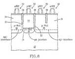
- the opening 26is used in defining different active device regions for the subsequent formation of semiconductor devices. Consistent with the terminology used in the present application, the area that will include the second semiconductor layer 16 as the active device layer will be referred to herein as second device region 28 , while the area that will include the first semiconductor layer 12 (as an epitaxial regrown layer, to be subsequently described) as the active device layer will be referred to herein as first device region 30 .
- an optional spacer 32can be formed in the opening 26 on the exposed sidewalls provided by the above processing steps.
- the optional spacer 32is formed by deposition and etching.
- the optional spacer 32can be comprised of an insulating material such as, for example, an oxide, nitride, oxynitride or any combination thereof.
- the optional spacer 32may be a single spacer, as shown, or it may comprise multiple spacers.
- FIG. 5Cshows the presence of optional spacers 32 in the structure.
- a semiconductor material 34is then formed on the exposed surface of the first semiconductor layer 12 to provide the structure shown, for example, in FIG. 5C .
- semiconductor material 34has a crystallographic orientation that is the same as the crystallographic orientation of the first semiconductor layer 12 . Although this regrown semiconductor layer will have the same surface orientation as the first semiconductor layer 12 , it can be of a different semiconductor material than the first semiconductor layer 12 .
- the semiconductor material 34may comprise any semiconductor material, such as Si, strained Si, SiGe, SiC, SiGeC or combinations thereof, which is capable of being formed utilizing a selective epitaxial growth method.
- Semiconductor material 34can be strained, unstrained, or it can be comprised of stained and unstrained layers, e.g., strained Si on a relaxed SiGe layer.
- semiconductor material 34is comprised of Si. In other preferred embodiments, the semiconductor material 34 is a strained Si layer that may or may not be located atop a relaxed SiGe alloy layer. In the present invention, semiconductor material 34 is referred to as a regrown semiconductor material.
- the semiconductor material 34can be grown, in some embodiments, higher than the patterned mask 24 ′ and then it is polished down to the patterned mask 24 ′.
- the regrown semiconductor material 34may be recessed at this point of the present invention utilizing a time etching process such as a timed RIE.
- a time etching processsuch as a timed RIE.
- One or more additional semiconductor layerscan be formed directly on top of the recessed surface. The semiconductor materials formed would each have the same crystallographic orientation as that of the first semiconductor layer 12 .
- the semiconductor material 34may need to be etched back to the same level as the second semiconductor layer 16 .
- This etchingcan be performed by dry etching, wet etching or oxidation of silicon and then stripping away the oxide.
- isolation regions 36are typically formed so as to isolate the first semiconductor active device region 30 from the second semiconductor active device region 28 .
- the isolation regions 36are formed utilizing processing steps that are well known to those skilled in the art including, for example, trench definition and etching; optionally lining the trench with a diffusion barrier; and filling the trench with a trench dielectric such as an oxide. After the trench fill, the structure may be planarized and an optional densification process step may be performed to densify the trench dielectric.
- well regionsare formed into the exposed semiconductor device layers, i.e., layer 16 or regrown semiconductor material 34 , by utilizing ion implantation and annealing, both of which are well known to those skilled in the art.
- the well regionsare designated by reference numeral 38 in FIG. 5E .
- the well regionsmay be n-type well regions or p-type well regions depending on the type of semiconductor device to be formed on each semiconductor layer, i.e., second semiconductor layer 16 and regrown semiconductor material 34 . For example, if the semiconductor device is a pFET, well region 38 will be an n-type well, while if the semiconductor device is an nFET, well region 38 is a p-type well.
- Doping of each wellis performed in different implant steps in which an implant mask is formed atop locations in which the specific dopant is not intended to be implanted into.
- the well regions 38serves as body contacts in the present application.
- the depth of the well regions 38can vary depending on the implant and annealing conditions as well as the type of dopant used.
- the first semiconductor device 52may be a pFET or an nFET
- the second semiconductor device 50may be an nFET or pFET, with the proviso that the first semiconductor device is different from the second semiconductor device and that the specific device is fabricating on a crystal orientation that provides a high performance device.
- the pFETs and nFETsare formed utilizing standard CMOS processing steps that are well known to those skilled in the art.
- Each FETincludes a gate dielectric, a gate conductor, an optional hard mask located atop the gate conductor, spacers located on sidewalls of at least the gate conductor, and source/drain diffusion regions. Note that the pFET is formed over the semiconductor material that has a (110) or (111) orientation, whereas the nFET is formed over a semiconductor surface having a (100) or (111) orientation.
- the resultant structure including bulk-like FETsis shown in FIG. 5E .
- the conductive (i.e., bonding) interface 14can be designed to be below the isolation regions 36 and the wells 38 .
- the interface 14should be below the n-well. Specifically, it should be outside the depletion region of the well pn junctions. The depletion width of a pn junction is reverse proportional to their doping level.
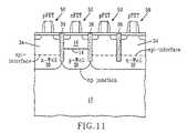
- strained Si processes contemplated by the present inventionwill be described with reference to the specific embodiments shown in FIGS. 12–16 . Unless otherwise specified, the processing steps and materials used above are used in the strained Si embodiments.
- a masking layer(hereinafter referred to as a “pad stack”) comprising a pad oxide 74 and a pad nitride 76 are then formed by deposition and the pad stack is subjected to lithography and etching so as to expose a portion of the second semiconductor layer 16 .
- the exposed portion of the second semiconductor layer 16is then etched stopping on, or within, the first semiconductor layer 12 .
- Optional spacer 32are then formed on each sidewall within the opening provided by the aforementioned etching step.
- the resultant structureis shown, for example, in FIG. 12C .
Landscapes
- Engineering & Computer Science (AREA)
- Physics & Mathematics (AREA)
- Condensed Matter Physics & Semiconductors (AREA)
- General Physics & Mathematics (AREA)
- Manufacturing & Machinery (AREA)
- Computer Hardware Design (AREA)
- Microelectronics & Electronic Packaging (AREA)
- Power Engineering (AREA)
- Metal-Oxide And Bipolar Metal-Oxide Semiconductor Integrated Circuits (AREA)
- Element Separation (AREA)
- Thin Film Transistor (AREA)
Abstract
Description
Claims (17)
Priority Applications (4)
| Application Number | Priority Date | Filing Date | Title |
|---|---|---|---|
| US10/799,380US7023057B2 (en) | 2003-10-29 | 2004-03-12 | CMOS on hybrid substrate with different crystal orientations using silicon-to-silicon direct wafer bonding |
| TW093131955ATWI317986B (en) | 2003-10-29 | 2004-10-21 | Cmos on hybrid substrate with different crystal orientations using silicon-to-silicon direct wafer bonding |
| CNB2004100870082ACN100361302C (en) | 2003-10-29 | 2004-10-22 | Hybrid substrates, integrated semiconductor structures, and methods of making them |
| JP2004310704AJP4328708B2 (en) | 2003-10-29 | 2004-10-26 | Manufacturing method of CMOS device and structure including CMOS device |
Applications Claiming Priority (2)
| Application Number | Priority Date | Filing Date | Title |
|---|---|---|---|
| US10/696,634US7023055B2 (en) | 2003-10-29 | 2003-10-29 | CMOS on hybrid substrate with different crystal orientations using silicon-to-silicon direct wafer bonding |
| US10/799,380US7023057B2 (en) | 2003-10-29 | 2004-03-12 | CMOS on hybrid substrate with different crystal orientations using silicon-to-silicon direct wafer bonding |
Related Parent Applications (1)
| Application Number | Title | Priority Date | Filing Date |
|---|---|---|---|
| US10/696,634Continuation-In-PartUS7023055B2 (en) | 2003-10-29 | 2003-10-29 | CMOS on hybrid substrate with different crystal orientations using silicon-to-silicon direct wafer bonding |
Publications (2)
| Publication Number | Publication Date |
|---|---|
| US20050093077A1 US20050093077A1 (en) | 2005-05-05 |
| US7023057B2true US7023057B2 (en) | 2006-04-04 |
Family
ID=34550154
Family Applications (3)
| Application Number | Title | Priority Date | Filing Date |
|---|---|---|---|
| US10/696,634Expired - Fee RelatedUS7023055B2 (en) | 2003-10-29 | 2003-10-29 | CMOS on hybrid substrate with different crystal orientations using silicon-to-silicon direct wafer bonding |
| US10/799,380Expired - LifetimeUS7023057B2 (en) | 2003-10-29 | 2004-03-12 | CMOS on hybrid substrate with different crystal orientations using silicon-to-silicon direct wafer bonding |
| US11/327,966Expired - Fee RelatedUS7364958B2 (en) | 2003-10-29 | 2006-01-09 | CMOS on hybrid substrate with different crystal orientations using silicon-to-silicon direct wafer bonding |
Family Applications Before (1)
| Application Number | Title | Priority Date | Filing Date |
|---|---|---|---|
| US10/696,634Expired - Fee RelatedUS7023055B2 (en) | 2003-10-29 | 2003-10-29 | CMOS on hybrid substrate with different crystal orientations using silicon-to-silicon direct wafer bonding |
Family Applications After (1)
| Application Number | Title | Priority Date | Filing Date |
|---|---|---|---|
| US11/327,966Expired - Fee RelatedUS7364958B2 (en) | 2003-10-29 | 2006-01-09 | CMOS on hybrid substrate with different crystal orientations using silicon-to-silicon direct wafer bonding |
Country Status (2)
| Country | Link |
|---|---|
| US (3) | US7023055B2 (en) |
| TW (1) | TWI317986B (en) |
Cited By (13)
| Publication number | Priority date | Publication date | Assignee | Title |
|---|---|---|---|---|
| US20040256700A1 (en)* | 2003-06-17 | 2004-12-23 | International Business Machines Corporation | High-performance CMOS devices on hybrid crystal oriented substrates |
| US7253034B2 (en)* | 2004-07-29 | 2007-08-07 | International Business Machines Corporation | Dual SIMOX hybrid orientation technology (HOT) substrates |
| US20080020521A1 (en)* | 2004-06-21 | 2008-01-24 | International Business Machines Corporation | Hybrid substrate technology for high-mobility planar and multiple-gate mosfets |
| US20080274595A1 (en)* | 2007-05-01 | 2008-11-06 | Spencer Gregory S | Dual substrate orientation or bulk on SOI integrations using oxidation for silicon epitaxy spacer formation |
| US20080290379A1 (en)* | 2005-08-19 | 2008-11-27 | International Business Machines Corporation | Dual trench isolation for cmos with hybrid orientations |
| US20090032842A1 (en)* | 2007-08-02 | 2009-02-05 | Lagally Max G | Nanomembrane structures having mixed crystalline orientations and compositions |
| US20090072276A1 (en)* | 2007-08-24 | 2009-03-19 | Kabushiki Kaisha Toshiba | Semiconductor wafer, semiconductor device and method of fabricating the same |
| US20100155788A1 (en)* | 2006-03-15 | 2010-06-24 | Shaheen Mohamad A | Formation of a multiple crystal orientation substrate |
| US20110254099A1 (en)* | 2009-12-01 | 2011-10-20 | Shanghai Institute of Microsystem and Information Technology Chinese Academy | Hybrid material accumulation mode GAA CMOSFET |
| US20110254101A1 (en)* | 2009-12-01 | 2011-10-20 | Shanghai Institute of Microsystem and Information Technology Chinese Academy | Hybrid material inversion mode gaa cmosfet |
| US8093084B2 (en) | 2009-04-30 | 2012-01-10 | Freescale Semiconductor, Inc. | Semiconductor device with photonics |
| CN102437158A (en)* | 2011-11-30 | 2012-05-02 | 上海华力微电子有限公司 | CMOS semiconductor device and method for manufacturing the same |
| US20130320401A1 (en)* | 2005-12-23 | 2013-12-05 | Infineon Technologies Ag | Mixed Orientation Semiconductor Device and Method |
Families Citing this family (83)
| Publication number | Priority date | Publication date | Assignee | Title |
|---|---|---|---|---|
| US7247534B2 (en) | 2003-11-19 | 2007-07-24 | International Business Machines Corporation | Silicon device on Si:C-OI and SGOI and method of manufacture |
| US20050116290A1 (en)* | 2003-12-02 | 2005-06-02 | De Souza Joel P. | Planar substrate with selected semiconductor crystal orientations formed by localized amorphization and recrystallization of stacked template layers |
| US7087965B2 (en)* | 2004-04-22 | 2006-08-08 | International Business Machines Corporation | Strained silicon CMOS on hybrid crystal orientations |
| TWI463526B (en)* | 2004-06-24 | 2014-12-01 | Ibm | Method for improving stress-induced CMOS components and components prepared by the method |
| US7172930B2 (en)* | 2004-07-02 | 2007-02-06 | International Business Machines Corporation | Strained silicon-on-insulator by anodization of a buried p+ silicon germanium layer |
| US7405436B2 (en)* | 2005-01-05 | 2008-07-29 | International Business Machines Corporation | Stressed field effect transistors on hybrid orientation substrate |
| US8138061B2 (en)* | 2005-01-07 | 2012-03-20 | International Business Machines Corporation | Quasi-hydrophobic Si-Si wafer bonding using hydrophilic Si surfaces and dissolution of interfacial bonding oxide |
| US20060175659A1 (en)* | 2005-02-07 | 2006-08-10 | International Business Machines Corporation | A cmos structure for body ties in ultra-thin soi (utsoi) substrates |
| US7538351B2 (en)* | 2005-03-23 | 2009-05-26 | Taiwan Semiconductor Manufacturing Co., Ltd. | Method for forming an SOI structure with improved carrier mobility and ESD protection |
| US7432149B2 (en)* | 2005-06-23 | 2008-10-07 | Taiwan Semiconductor Manufacturing Company, Ltd. | CMOS on SOI substrates with hybrid crystal orientations |
| US7611937B2 (en)* | 2005-06-24 | 2009-11-03 | Taiwan Semiconductor Manufacturing Company, Ltd. | High performance transistors with hybrid crystal orientations |
| US7382029B2 (en)* | 2005-07-29 | 2008-06-03 | International Business Machines Corporation | Method and apparatus for improving integrated circuit device performance using hybrid crystal orientations |
| KR100655437B1 (en)* | 2005-08-09 | 2006-12-08 | 삼성전자주식회사 | Semiconductor Wafer and Manufacturing Method Thereof |
| US7524707B2 (en)* | 2005-08-23 | 2009-04-28 | Freescale Semiconductor, Inc. | Modified hybrid orientation technology |
| US7986029B2 (en)* | 2005-11-08 | 2011-07-26 | Taiwan Semiconductor Manufacturing Company, Ltd. | Dual SOI structure |
| US7569466B2 (en)* | 2005-12-16 | 2009-08-04 | International Business Machines Corporation | Dual metal gate self-aligned integration |
| US7436034B2 (en)* | 2005-12-19 | 2008-10-14 | International Business Machines Corporation | Metal oxynitride as a pFET material |
| US7432567B2 (en)* | 2005-12-28 | 2008-10-07 | International Business Machines Corporation | Metal gate CMOS with at least a single gate metal and dual gate dielectrics |
| US20070152276A1 (en)* | 2005-12-30 | 2007-07-05 | International Business Machines Corporation | High performance CMOS circuits, and methods for fabricating the same |
| US7833849B2 (en) | 2005-12-30 | 2010-11-16 | International Business Machines Corporation | Method of fabricating a semiconductor structure including one device region having a metal gate electrode located atop a thinned polygate electrode |
| US7425497B2 (en) | 2006-01-20 | 2008-09-16 | International Business Machines Corporation | Introduction of metal impurity to change workfunction of conductive electrodes |
| JP4564929B2 (en)* | 2006-02-21 | 2010-10-20 | キヤノン株式会社 | Method for forming a three-dimensional photonic crystal |
| US7700420B2 (en)* | 2006-04-12 | 2010-04-20 | Freescale Semiconductor, Inc. | Integrated circuit with different channel materials for P and N channel transistors and method therefor |
| US7268028B1 (en)* | 2006-04-17 | 2007-09-11 | International Business Machines Corporation | Well isolation trenches (WIT) for CMOS devices |
| US7396407B2 (en)* | 2006-04-18 | 2008-07-08 | International Business Machines Corporation | Trench-edge-defect-free recrystallization by edge-angle-optimized solid phase epitaxy: method and applications to hybrid orientation substrates |
| US7670927B2 (en)* | 2006-05-16 | 2010-03-02 | International Business Machines Corporation | Double-sided integrated circuit chips |
| US8013342B2 (en)* | 2007-11-14 | 2011-09-06 | International Business Machines Corporation | Double-sided integrated circuit chips |
| US7670928B2 (en)* | 2006-06-14 | 2010-03-02 | Intel Corporation | Ultra-thin oxide bonding for S1 to S1 dual orientation bonding |
| US20080048269A1 (en)* | 2006-08-25 | 2008-02-28 | International Business Machines Corporation | Method of fabricating structure for integrated circuit incorporating hybrid orientation technology and trench isolation regions |
| US7595232B2 (en)* | 2006-09-07 | 2009-09-29 | International Business Machines Corporation | CMOS devices incorporating hybrid orientation technology (HOT) with embedded connectors |
| US7504301B2 (en)* | 2006-09-28 | 2009-03-17 | Advanced Micro Devices, Inc. | Stressed field effect transistor and methods for its fabrication |
| US8016941B2 (en)* | 2007-02-05 | 2011-09-13 | Infineon Technologies Ag | Method and apparatus for manufacturing a semiconductor |
| US7611979B2 (en)* | 2007-02-12 | 2009-11-03 | International Business Machines Corporation | Metal gates with low charge trapping and enhanced dielectric reliability characteristics for high-k gate dielectric stacks |
| US7608522B2 (en)* | 2007-03-11 | 2009-10-27 | United Microelectronics Corp. | Method for fabricating a hybrid orientation substrate |
| US7547641B2 (en)* | 2007-06-05 | 2009-06-16 | International Business Machines Corporation | Super hybrid SOI CMOS devices |
| US20090008725A1 (en)* | 2007-07-03 | 2009-01-08 | International Business Machines Corporation | Method for deposition of an ultra-thin electropositive metal-containing cap layer |
| US8115254B2 (en) | 2007-09-25 | 2012-02-14 | International Business Machines Corporation | Semiconductor-on-insulator structures including a trench containing an insulator stressor plug and method of fabricating same |
| US8105960B2 (en)* | 2007-10-09 | 2012-01-31 | International Business Machines Corporation | Self-assembled sidewall spacer |
| US7808020B2 (en)* | 2007-10-09 | 2010-10-05 | International Business Machines Corporation | Self-assembled sidewall spacer |
| US7696573B2 (en)* | 2007-10-31 | 2010-04-13 | International Business Machines Corporation | Multiple crystallographic orientation semiconductor structures |
| US8492846B2 (en) | 2007-11-15 | 2013-07-23 | International Business Machines Corporation | Stress-generating shallow trench isolation structure having dual composition |
| US8039401B2 (en)* | 2007-12-14 | 2011-10-18 | Fairchild Semiconductor Corporation | Structure and method for forming hybrid substrate |
| US8211786B2 (en) | 2008-02-28 | 2012-07-03 | International Business Machines Corporation | CMOS structure including non-planar hybrid orientation substrate with planar gate electrodes and method for fabrication |
| JP2010072209A (en)* | 2008-09-17 | 2010-04-02 | Fuji Xerox Co Ltd | Electrostatic charge image developing toner, method for manufacturing electrostatic charge image developing toner, electrostatic charge image developing developer, and image forming device |
| US8053304B2 (en)* | 2009-02-24 | 2011-11-08 | Taiwan Semiconductor Manufacturing Company, Ltd. | Method of forming high-mobility devices including epitaxially growing a semiconductor layer on a dislocation-blocking layer in a recess formed in a semiconductor substrate |
| US8227307B2 (en)* | 2009-06-24 | 2012-07-24 | International Business Machines Corporation | Method for removing threshold voltage adjusting layer with external acid diffusion process |
| US8105892B2 (en)* | 2009-08-18 | 2012-01-31 | International Business Machines Corporation | Thermal dual gate oxide device integration |
| US8022488B2 (en) | 2009-09-24 | 2011-09-20 | International Business Machines Corporation | High-performance FETs with embedded stressors |
| US7943458B2 (en)* | 2009-10-06 | 2011-05-17 | International Business Machines Corporation | Methods for obtaining gate stacks with tunable threshold voltage and scaling |
| US8680617B2 (en)* | 2009-10-06 | 2014-03-25 | International Business Machines Corporation | Split level shallow trench isolation for area efficient body contacts in SOI MOSFETS |
| US8288222B2 (en) | 2009-10-20 | 2012-10-16 | International Business Machines Corporation | Application of cluster beam implantation for fabricating threshold voltage adjusted FETs |
| US8035141B2 (en) | 2009-10-28 | 2011-10-11 | International Business Machines Corporation | Bi-layer nFET embedded stressor element and integration to enhance drive current |
| CN101710585B (en)* | 2009-12-01 | 2011-04-27 | 中国科学院上海微系统与信息技术研究所 | Mixed Orientation Accumulation All-around Gate CMOS Field Effect Transistor |
| CN101719500B (en)* | 2009-12-01 | 2011-09-21 | 中国科学院上海微系统与信息技术研究所 | Mixed material inversion mode all-around gate CMOS field effect transistor |
| US8445974B2 (en)* | 2010-01-07 | 2013-05-21 | International Business Machines Corporation | Asymmetric FET including sloped threshold voltage adjusting material layer and method of fabricating same |
| US8299530B2 (en) | 2010-03-04 | 2012-10-30 | International Business Machines Corporation | Structure and method to fabricate pFETS with superior GIDL by localizing workfunction |
| US8450807B2 (en) | 2010-03-09 | 2013-05-28 | International Business Machines Corporation | MOSFETs with reduced contact resistance |
| US8236660B2 (en) | 2010-04-21 | 2012-08-07 | International Business Machines Corporation | Monolayer dopant embedded stressor for advanced CMOS |
| US8299535B2 (en) | 2010-06-25 | 2012-10-30 | International Business Machines Corporation | Delta monolayer dopants epitaxy for embedded source/drain silicide |
| US8361889B2 (en) | 2010-07-06 | 2013-01-29 | International Business Machines Corporation | Strained semiconductor-on-insulator by addition and removal of atoms in a semiconductor-on-insulator |
| US8659054B2 (en) | 2010-10-15 | 2014-02-25 | International Business Machines Corporation | Method and structure for pFET junction profile with SiGe channel |
| US8962417B2 (en) | 2010-10-15 | 2015-02-24 | International Business Machines Corporation | Method and structure for pFET junction profile with SiGe channel |
| US8466473B2 (en) | 2010-12-06 | 2013-06-18 | International Business Machines Corporation | Structure and method for Vt tuning and short channel control with high k/metal gate MOSFETs |
| US8536656B2 (en) | 2011-01-10 | 2013-09-17 | International Business Machines Corporation | Self-aligned contacts for high k/metal gate process flow |
| US8643115B2 (en) | 2011-01-14 | 2014-02-04 | International Business Machines Corporation | Structure and method of Tinv scaling for high κ metal gate technology |
| US8432002B2 (en)* | 2011-06-28 | 2013-04-30 | International Business Machines Corporation | Method and structure for low resistive source and drain regions in a replacement metal gate process flow |
| KR20130054010A (en)* | 2011-11-16 | 2013-05-24 | 삼성전자주식회사 | Semiconductor device using iii-v group material and method of manufacturing the same |
| US8610172B2 (en)* | 2011-12-15 | 2013-12-17 | International Business Machines Corporation | FETs with hybrid channel materials |
| US9368578B2 (en)* | 2013-02-04 | 2016-06-14 | Globalfoundries Inc. | Methods of forming substrates comprised of different semiconductor materials and the resulting device |
| US9059095B2 (en) | 2013-04-22 | 2015-06-16 | International Business Machines Corporation | Self-aligned borderless contacts using a photo-patternable dielectric material as a replacement contact |
| US8999791B2 (en) | 2013-05-03 | 2015-04-07 | International Business Machines Corporation | Formation of semiconductor structures with variable gate lengths |
| US9214567B2 (en) | 2013-09-06 | 2015-12-15 | Globalfoundries Inc. | Nanowire compatible E-fuse |
| US8951868B1 (en) | 2013-11-05 | 2015-02-10 | International Business Machines Corporation | Formation of functional gate structures with different critical dimensions using a replacement gate process |
| US9595525B2 (en) | 2014-02-10 | 2017-03-14 | International Business Machines Corporation | Semiconductor device including nanowire transistors with hybrid channels |
| US9093425B1 (en) | 2014-02-11 | 2015-07-28 | International Business Machines Corporation | Self-aligned liner formed on metal semiconductor alloy contacts |
| US9184290B2 (en) | 2014-04-02 | 2015-11-10 | International Business Machines Corporation | Method of forming well-controlled extension profile in MOSFET by silicon germanium based sacrificial layer |
| US9293375B2 (en) | 2014-04-24 | 2016-03-22 | International Business Machines Corporation | Selectively grown self-aligned fins for deep isolation integration |
| US9490161B2 (en)* | 2014-04-29 | 2016-11-08 | International Business Machines Corporation | Channel SiGe devices with multiple threshold voltages on hybrid oriented substrates, and methods of manufacturing same |
| US9331076B2 (en) | 2014-05-02 | 2016-05-03 | International Business Machines Corporation | Group III nitride integration with CMOS technology |
| US9412840B1 (en) | 2015-05-06 | 2016-08-09 | International Business Machines Corporation | Sacrificial layer for replacement metal semiconductor alloy contact formation |
| US10593600B2 (en) | 2016-02-24 | 2020-03-17 | International Business Machines Corporation | Distinct gate stacks for III-V-based CMOS circuits comprising a channel cap |
| US10062693B2 (en)* | 2016-02-24 | 2018-08-28 | International Business Machines Corporation | Patterned gate dielectrics for III-V-based CMOS circuits |
| KR20220058042A (en) | 2020-10-30 | 2022-05-09 | 삼성전자주식회사 | Semiconductor wafer and method for fabricating the same |
Citations (3)
| Publication number | Priority date | Publication date | Assignee | Title |
|---|---|---|---|---|
| US20040075141A1 (en)* | 2002-10-17 | 2004-04-22 | Renesas Technology Corp. | Semiconductor device and method of manufacturing same |
| US20040195646A1 (en)* | 2003-04-04 | 2004-10-07 | Yee-Chia Yeo | Silicon-on-insulator chip with multiple crystal orientations |
| US20050082531A1 (en)* | 2003-10-17 | 2005-04-21 | International Business Machines Corporaton | Double silicon-on-insulator (SOI) metal oxide semiconductor field effect transistor (MOSFET) structures |
Family Cites Families (13)
| Publication number | Priority date | Publication date | Assignee | Title |
|---|---|---|---|---|
| JP2685819B2 (en)* | 1988-03-31 | 1997-12-03 | 株式会社東芝 | Dielectric isolated semiconductor substrate and manufacturing method thereof |
| JP3734849B2 (en)* | 1995-05-08 | 2006-01-11 | 三菱電機株式会社 | Manufacturing method of semiconductor laser device |
| JP2001068708A (en)* | 1999-08-30 | 2001-03-16 | Sanyo Electric Co Ltd | Semiconductor element, solar-battery element and manufacture of the semiconductor element |
| US6476462B2 (en)* | 1999-12-28 | 2002-11-05 | Texas Instruments Incorporated | MOS-type semiconductor device and method for making same |
| JP2002134374A (en)* | 2000-10-25 | 2002-05-10 | Mitsubishi Electric Corp | Semiconductor wafer, its manufacturing method and its manufacturing apparatus |
| US6784071B2 (en)* | 2003-01-31 | 2004-08-31 | Taiwan Semiconductor Manufacturing Company, Ltd. | Bonded SOI wafer with <100> device layer and <110> substrate for performance improvement |
| US7153757B2 (en)* | 2002-08-29 | 2006-12-26 | Analog Devices, Inc. | Method for direct bonding two silicon wafers for minimising interfacial oxide and stresses at the bond interface, and an SOI structure |
| JP2004119943A (en)* | 2002-09-30 | 2004-04-15 | Renesas Technology Corp | Semiconductor wafer and method of manufacturing the same |
| US6759277B1 (en)* | 2003-02-27 | 2004-07-06 | Sharp Laboratories Of America, Inc. | Crystalline silicon die array and method for assembling crystalline silicon sheets onto substrates |
| US7329923B2 (en)* | 2003-06-17 | 2008-02-12 | International Business Machines Corporation | High-performance CMOS devices on hybrid crystal oriented substrates |
| US6830962B1 (en)* | 2003-08-05 | 2004-12-14 | International Business Machines Corporation | Self-aligned SOI with different crystal orientation using wafer bonding and SIMOX processes |
| US6815278B1 (en)* | 2003-08-25 | 2004-11-09 | International Business Machines Corporation | Ultra-thin silicon-on-insulator and strained-silicon-direct-on-insulator with hybrid crystal orientations |
| US6821826B1 (en)* | 2003-09-30 | 2004-11-23 | International Business Machines Corporation | Three dimensional CMOS integrated circuits having device layers built on different crystal oriented wafers |
- 2003
- 2003-10-29USUS10/696,634patent/US7023055B2/ennot_activeExpired - Fee Related
- 2004
- 2004-03-12USUS10/799,380patent/US7023057B2/ennot_activeExpired - Lifetime
- 2004-10-21TWTW093131955Apatent/TWI317986B/ennot_activeIP Right Cessation
- 2006
- 2006-01-09USUS11/327,966patent/US7364958B2/ennot_activeExpired - Fee Related
Patent Citations (3)
| Publication number | Priority date | Publication date | Assignee | Title |
|---|---|---|---|---|
| US20040075141A1 (en)* | 2002-10-17 | 2004-04-22 | Renesas Technology Corp. | Semiconductor device and method of manufacturing same |
| US20040195646A1 (en)* | 2003-04-04 | 2004-10-07 | Yee-Chia Yeo | Silicon-on-insulator chip with multiple crystal orientations |
| US20050082531A1 (en)* | 2003-10-17 | 2005-04-21 | International Business Machines Corporaton | Double silicon-on-insulator (SOI) metal oxide semiconductor field effect transistor (MOSFET) structures |
Cited By (24)
| Publication number | Priority date | Publication date | Assignee | Title |
|---|---|---|---|---|
| US20040256700A1 (en)* | 2003-06-17 | 2004-12-23 | International Business Machines Corporation | High-performance CMOS devices on hybrid crystal oriented substrates |
| US7485506B2 (en)* | 2004-06-21 | 2009-02-03 | International Business Machines Corporation | Hybrid substrate technology for high-mobility planar and multiple-gate MOSFETS |
| US20080020521A1 (en)* | 2004-06-21 | 2008-01-24 | International Business Machines Corporation | Hybrid substrate technology for high-mobility planar and multiple-gate mosfets |
| US7253034B2 (en)* | 2004-07-29 | 2007-08-07 | International Business Machines Corporation | Dual SIMOX hybrid orientation technology (HOT) substrates |
| US20080290379A1 (en)* | 2005-08-19 | 2008-11-27 | International Business Machines Corporation | Dual trench isolation for cmos with hybrid orientations |
| US8097516B2 (en) | 2005-08-19 | 2012-01-17 | International Business Machines Corporation | Dual trench isolation for CMOS with hybrid orientations |
| US9355887B2 (en) | 2005-08-19 | 2016-05-31 | Globalfoundries Inc. | Dual trench isolation for CMOS with hybrid orientations |
| US9607986B2 (en)* | 2005-12-23 | 2017-03-28 | Infineon Technologies Ag | Mixed orientation semiconductor device and method |
| US20130320401A1 (en)* | 2005-12-23 | 2013-12-05 | Infineon Technologies Ag | Mixed Orientation Semiconductor Device and Method |
| US20100155788A1 (en)* | 2006-03-15 | 2010-06-24 | Shaheen Mohamad A | Formation of a multiple crystal orientation substrate |
| US7790528B2 (en) | 2007-05-01 | 2010-09-07 | Freescale Semiconductor, Inc. | Dual substrate orientation or bulk on SOI integrations using oxidation for silicon epitaxy spacer formation |
| US20080274595A1 (en)* | 2007-05-01 | 2008-11-06 | Spencer Gregory S | Dual substrate orientation or bulk on SOI integrations using oxidation for silicon epitaxy spacer formation |
| US20090032842A1 (en)* | 2007-08-02 | 2009-02-05 | Lagally Max G | Nanomembrane structures having mixed crystalline orientations and compositions |
| US8803195B2 (en) | 2007-08-02 | 2014-08-12 | Wisconsin Alumni Research Foundation | Nanomembrane structures having mixed crystalline orientations and compositions |
| US8039843B2 (en) | 2007-08-24 | 2011-10-18 | Kabushiki Kaisha Toshiba | Semiconductor wafer, semiconductor device and method of fabricating the same |
| US20090072276A1 (en)* | 2007-08-24 | 2009-03-19 | Kabushiki Kaisha Toshiba | Semiconductor wafer, semiconductor device and method of fabricating the same |
| US8093084B2 (en) | 2009-04-30 | 2012-01-10 | Freescale Semiconductor, Inc. | Semiconductor device with photonics |
| US8242564B2 (en) | 2009-04-30 | 2012-08-14 | Freescale Semiconductor, Inc. | Semiconductor device with photonics |
| US20110254101A1 (en)* | 2009-12-01 | 2011-10-20 | Shanghai Institute of Microsystem and Information Technology Chinese Academy | Hybrid material inversion mode gaa cmosfet |
| US8330228B2 (en)* | 2009-12-01 | 2012-12-11 | Shanghai Institute Of Microsystem And Information Technology, Chinese Academy Of Sciences | Hybrid material inversion mode GAA CMOSFET |
| US8274118B2 (en)* | 2009-12-01 | 2012-09-25 | Shanghai Institute Of Microsystem And Information Technology, Chinese Academy Of Sciences | Hybrid material accumulation mode GAA CMOSFET |
| US20110254099A1 (en)* | 2009-12-01 | 2011-10-20 | Shanghai Institute of Microsystem and Information Technology Chinese Academy | Hybrid material accumulation mode GAA CMOSFET |
| CN102437158B (en)* | 2011-11-30 | 2015-10-28 | 上海华力微电子有限公司 | Cmos semiconductor device and manufacture method thereof |
| CN102437158A (en)* | 2011-11-30 | 2012-05-02 | 上海华力微电子有限公司 | CMOS semiconductor device and method for manufacturing the same |
Also Published As
| Publication number | Publication date |
|---|---|
| TWI317986B (en) | 2009-12-01 |
| US7364958B2 (en) | 2008-04-29 |
| TW200524088A (en) | 2005-07-16 |
| US20050093104A1 (en) | 2005-05-05 |
| US20050093077A1 (en) | 2005-05-05 |
| US7023055B2 (en) | 2006-04-04 |
| US20060108643A1 (en) | 2006-05-25 |
Similar Documents
| Publication | Publication Date | Title |
|---|---|---|
| US7023057B2 (en) | CMOS on hybrid substrate with different crystal orientations using silicon-to-silicon direct wafer bonding | |
| US9355887B2 (en) | Dual trench isolation for CMOS with hybrid orientations | |
| US7087965B2 (en) | Strained silicon CMOS on hybrid crystal orientations | |
| US7393732B2 (en) | Double silicon-on-insulator (SOI) metal oxide semiconductor field effect transistor (MOSFET) structures | |
| US7915100B2 (en) | Hybrid orientation CMOS with partial insulation process | |
| US7833854B2 (en) | Structure and method of fabricating a hybrid substrate for high-performance hybrid-orientation silicon-on-insulator CMOS devices | |
| US6830962B1 (en) | Self-aligned SOI with different crystal orientation using wafer bonding and SIMOX processes | |
| US7253034B2 (en) | Dual SIMOX hybrid orientation technology (HOT) substrates | |
| US7687365B2 (en) | CMOS structure for body ties in ultra-thin SOI (UTSOI) substrates | |
| US7385257B2 (en) | Hybrid orientation SOI substrates, and method for forming the same | |
| JP4328708B2 (en) | Manufacturing method of CMOS device and structure including CMOS device | |
| US7250656B2 (en) | Hybrid-orientation technology buried n-well design |
Legal Events
| Date | Code | Title | Description |
|---|---|---|---|
| AS | Assignment | Owner name:INTERNATIONAL BUSINESS MACHINES CORPORATION, NEW Y Free format text:ASSIGNMENT OF ASSIGNORS INTEREST;ASSIGNORS:IEONG, MEIKEI;REZNICEK, ALEXANDER;YANG, MIN;REEL/FRAME:014713/0989;SIGNING DATES FROM 20040309 TO 20040310 | |
| STCF | Information on status: patent grant | Free format text:PATENTED CASE | |
| CC | Certificate of correction | ||
| FPAY | Fee payment | Year of fee payment:4 | |
| REMI | Maintenance fee reminder mailed | ||
| FPAY | Fee payment | Year of fee payment:8 | |
| SULP | Surcharge for late payment | Year of fee payment:7 | |
| AS | Assignment | Owner name:GLOBALFOUNDRIES U.S. 2 LLC, NEW YORK Free format text:ASSIGNMENT OF ASSIGNORS INTEREST;ASSIGNOR:INTERNATIONAL BUSINESS MACHINES CORPORATION;REEL/FRAME:036550/0001 Effective date:20150629 | |
| AS | Assignment | Owner name:GLOBALFOUNDRIES INC., CAYMAN ISLANDS Free format text:ASSIGNMENT OF ASSIGNORS INTEREST;ASSIGNORS:GLOBALFOUNDRIES U.S. 2 LLC;GLOBALFOUNDRIES U.S. INC.;REEL/FRAME:036779/0001 Effective date:20150910 | |
| MAFP | Maintenance fee payment | Free format text:PAYMENT OF MAINTENANCE FEE, 12TH YEAR, LARGE ENTITY (ORIGINAL EVENT CODE: M1553) Year of fee payment:12 | |
| AS | Assignment | Owner name:WILMINGTON TRUST, NATIONAL ASSOCIATION, DELAWARE Free format text:SECURITY AGREEMENT;ASSIGNOR:GLOBALFOUNDRIES INC.;REEL/FRAME:049490/0001 Effective date:20181127 | |
| AS | Assignment | Owner name:GLOBALFOUNDRIES U.S. INC., CALIFORNIA Free format text:ASSIGNMENT OF ASSIGNORS INTEREST;ASSIGNOR:GLOBALFOUNDRIES INC.;REEL/FRAME:054633/0001 Effective date:20201022 | |
| AS | Assignment | Owner name:GLOBALFOUNDRIES INC., CAYMAN ISLANDS Free format text:RELEASE BY SECURED PARTY;ASSIGNOR:WILMINGTON TRUST, NATIONAL ASSOCIATION;REEL/FRAME:054636/0001 Effective date:20201117 | |
| AS | Assignment | Owner name:GLOBALFOUNDRIES U.S. INC., NEW YORK Free format text:RELEASE BY SECURED PARTY;ASSIGNOR:WILMINGTON TRUST, NATIONAL ASSOCIATION;REEL/FRAME:056987/0001 Effective date:20201117 |