US7023031B2 - CMOS imager having on-chip ROM - Google Patents
CMOS imager having on-chip ROMDownload PDFInfo
- Publication number
- US7023031B2 US7023031B2US10/222,827US22282702AUS7023031B2US 7023031 B2US7023031 B2US 7023031B2US 22282702 AUS22282702 AUS 22282702AUS 7023031 B2US7023031 B2US 7023031B2
- Authority
- US
- United States
- Prior art keywords
- column
- row
- read
- access transistor
- transistor
- Prior art date
- Legal status (The legal status is an assumption and is not a legal conclusion. Google has not performed a legal analysis and makes no representation as to the accuracy of the status listed.)
- Expired - Lifetime, expires
Links
Images


Classifications
- H—ELECTRICITY
- H04—ELECTRIC COMMUNICATION TECHNIQUE
- H04N—PICTORIAL COMMUNICATION, e.g. TELEVISION
- H04N25/00—Circuitry of solid-state image sensors [SSIS]; Control thereof
- H—ELECTRICITY
- H04—ELECTRIC COMMUNICATION TECHNIQUE
- H04N—PICTORIAL COMMUNICATION, e.g. TELEVISION
- H04N25/00—Circuitry of solid-state image sensors [SSIS]; Control thereof
- H04N25/60—Noise processing, e.g. detecting, correcting, reducing or removing noise
- H04N25/68—Noise processing, e.g. detecting, correcting, reducing or removing noise applied to defects
- H—ELECTRICITY
- H04—ELECTRIC COMMUNICATION TECHNIQUE
- H04N—PICTORIAL COMMUNICATION, e.g. TELEVISION
- H04N25/00—Circuitry of solid-state image sensors [SSIS]; Control thereof
- H04N25/70—SSIS architectures; Circuits associated therewith
- H04N25/76—Addressed sensors, e.g. MOS or CMOS sensors
- H—ELECTRICITY
- H10—SEMICONDUCTOR DEVICES; ELECTRIC SOLID-STATE DEVICES NOT OTHERWISE PROVIDED FOR
- H10F—INORGANIC SEMICONDUCTOR DEVICES SENSITIVE TO INFRARED RADIATION, LIGHT, ELECTROMAGNETIC RADIATION OF SHORTER WAVELENGTH OR CORPUSCULAR RADIATION
- H10F39/00—Integrated devices, or assemblies of multiple devices, comprising at least one element covered by group H10F30/00, e.g. radiation detectors comprising photodiode arrays
- H10F39/10—Integrated devices
- H10F39/12—Image sensors
- H10F39/18—Complementary metal-oxide-semiconductor [CMOS] image sensors; Photodiode array image sensors
- H—ELECTRICITY
- H10—SEMICONDUCTOR DEVICES; ELECTRIC SOLID-STATE DEVICES NOT OTHERWISE PROVIDED FOR
- H10F—INORGANIC SEMICONDUCTOR DEVICES SENSITIVE TO INFRARED RADIATION, LIGHT, ELECTROMAGNETIC RADIATION OF SHORTER WAVELENGTH OR CORPUSCULAR RADIATION
- H10F39/00—Integrated devices, or assemblies of multiple devices, comprising at least one element covered by group H10F30/00, e.g. radiation detectors comprising photodiode arrays
- H10F39/80—Constructional details of image sensors
- H10F39/803—Pixels having integrated switching, control, storage or amplification elements
Definitions
- the present inventionrelates generally to CMOS image sensors and in particular to a CMOS image sensor provided with an on-chip Read Only Memory (ROM).
- ROMRead Only Memory
- Image sensing devicesare known that employ light detecting elements such as photodiodes or photo-transistors formed using complementary metal oxide semiconductor (CMOS) techniques.
- CMOScomplementary metal oxide semiconductor
- the imaging devicesgenerally include an array of pixels containing the light detecting elements arranged on a chip.
- an integrated circuit imaging device formed using a CMOS processhas an image sensor pixel array with associated row and column conductors and decoders, an analog signal path including a sample and hold circuit for reading pixel signals from the column conductors, a digital to analog converter for digitizing the analog pixel signals, a controller for controlling array read out operations, a pixel processor for processing digital pixel signals, and an input/output (I/O) port all fabricated on a single chip.
- the controllermanages operation of the read out of the image sensor array, the analog signal path and the analog digital converter, and may also operate as the pixel processor.
- each imaging pixel arrayis usually tested individually. Tests detect defective pixel circuits, pixel signal level, and other array attributes, and the information is stored based on lot and individual device identification numbers. The information developed during testing can be utilized to enhance the operation of the device by, for example, compensating for defective pixels, differing pixel signal levels, and other tested pixel attributes.
- U.S. Pat. No. 6,396,539 to Heller et al.discloses a CMOS imager with an on-chip programmable memory for storing pixel and identification information for a CMOS sensor array.
- the preferred embodiment disclosed by Heller et al.is based on a flash memory, which is complex and bulky. It would be desirable to provide an image sensor having on clip programmable read only memory employing a simple and compact circuit for reading and writing data, and which requires no difficult processing for forming the memory. A simple and easy way to store pixel array information on-chip for later use is also desirable.
- the present inventionprovides a CMOS image sensor formed on a chip and having a simplified ROM circuit disposed on the same chip for recording pixel information, for example, identification numbers, pixel defect locations, chip-by-chip variations such as pixel signal bias, and/or gain values and other manufacturing and/or test data. Testing results and repair solutions can be written to the ROM during post-production testing. A simple circuit for writing information to, and reading information from, the ROM is also provided.
- information about the image sensing arraysuch as identification numbers and pixel data obtained during manufacture and/or testing of the pixel array is saved to the on-chip ROM by applying high voltage/current to selected bits.
- the applied voltagebreaks the polysilicon fuse.
- the broken and unbroken fusesdefine bit patterns representing the stored information.
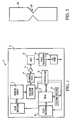
- FIG. 1is a simplified block diagram of an imaging sensor with an on-chip ROM in accordance with an exemplary embodiment of the invention
- FIG. 2is a schematic diagram of on-chip ROM and a read/write circuit as used in the imaging sensor of FIG. 1 in accordance with an exemplary embodiment of the invention.
- FIG. 3is a schematic representation of a memory cell fuse used in the imaging sensor of FIG. 1 in accordance with an exemplary embodiment of the invention.
- Imaging sensor 2preferably is formed by a CMOS process on a semiconductor substrate 6 (e.g., silicon substrate).
- the pixels within a sensor array 8may be formed with photodiodes as the light sensing element.
- Controller 10operates the row and column decoders and other signals to enable read out of analog pixel read out and charge accumulation signals row-by-row and column-by-column within a row to sample and hold circuit 9 as known in the art.
- the output of sample and hold circuitis amplified by amplifier 11 and is converted to digital signals by analog-to-digital converter 13 .
- a pixel processor 21digitally process the pixel information and supplies it to I/O port 16 .
- Controller 10also accesses memory cells of ROM 4 through a row address decoder 12 and a column address decoder 14 . As shown in FIG. 1 , ROM 4 is included on semiconductor substrate 6 along with imaging sensor 8 and controller 10 and other imager components.
- FIG. 2A circuit diagram of a portion of ROM 4 is shown in FIG. 2 .
- ROM 4includes an array of breakable fuses arranged in rows and columns. Each breakable fuse represents a memory cell of the ROM 4 .
- Representative fusesare designated as 20 , 22 , 24 , and 26 in FIG. 2 , although the fuse array can be extended to any number of rows and columns as determined by data storage requirements and space limitations.
- Each fuseis coupled between a row line and a column line.
- Fuse 20for example, is coupled between row line 30 and column line 34 .
- the fuse arrayis formed on-chip during fabrication of the other components shown in FIG. 1 .
- Fuse 20is a conductor formed of, for example, polysilicon, and includes a narrowed portion 38 which is subject to breakage when a high voltage is applied across the fuse.
- the fuse 20is shown as having a polysilicon strip portion 38 necked down by a pair of V-shaped notches, providing a simple, easily manufactured fuse arrangement. Other arrangements which allow for fuse severance using an elevated voltage may also be used.
- individual fusesare selected for writing by way of row and column switching transistors accessed by controller 10 through row and column address decoder 12 , 14 .
- Individual rowsare selected by way of row access transistors 40 and 42 , for example, coupled to rows 30 and 32 , respectively.
- Individual columnsare selected by column transistors 44 and 46 , having one source/drain connection coupled to columns 34 and 36 , respectively and the other source/drain connection connected to ground.
- Vprogrepresenting a voltage which is higher than a read voltage
- Vprogis of sufficient magnitude to break the narrowed section of the polysilicon fuse. Programming continues in this manner until all of the data is stored appropriately in the fuse array as fuse elements which are broken or not in a data information pattern.
- Data stored in ROM 4is accessed by the row and column decoders 12 , 14 and reading the selected fuse and/or fuses to determine the stored data.
- a blown fusehaving a high resistance and a large voltage drop, is read as one logic state (e.g., 1), while a non-blown fuse having a low resistance is read as another logic state (e.g., 0).
- a voltage Vddis applied to the fuse from the row line, which voltage is lower than the programming voltage Vprog.
- the contents of the memory cellsare (e.g., logic HIGH, or logic LOW) are read column by column onto line 53 by switching transistors 48 , 50 .
- Line 53is connected to inverter 54 which provides a logic output signal in accordance with a broken or unbroken state of read fuses 54 .
- the programming and read out of ROM memory 4occurs under control of a program and read out circuit which may conveniently be implemented within controller 10 which supplies row and column addresses for programming and read out functions to row 12 and column 14 decoders, and which controls transistor switches 61 to supply either a programming voltage Vprog or a read voltage Vdd to the source terminals of the row select transistors 40 , 42 , depending on whether a programming or read out operation is to occur. Controller 10 also controls transistor selection switches 63 to supply a selected column line signal from column decoder 14 to one of a programming column select switch, e.g., 44 or a read column select switch, e.g., 48 , again depending on whether a programming or read out operation is to occur.
- the program and read out circuit for ROM memory 4can also be implemented independently of controller 10 .
- Pixel formation which can be stored in the ROM according to the present inventionincludes identification data concerning manufacturing conditions and test results.
- Test resultscan include defective pixel location and types of defects.
- Information on pixel dark currentscan be stored, as well as reference temperature at which the pixels generate a desired output voltage under predetermined illumination conditions. Pixels that generate hot spots on dark spots can also be identified in the ROM, along with data indicating signal intensity.
- package/die informationcan be stored, along with camera information when the imager is used with a camera.
- ROM row or column redundancy informationcan also be stored in the form of programmed replacement rows or columns of memory elements.
- breakable fuses formed of polysiliconhave been disclosed above, any conductor used in the CMOS process can be used, as long as it can be configured to break under the noted programming conditions and can be read as described.
- the present inventionprovides a simple apparatus and method for storing data regarding a CMOS sensor array 8 in an on-chip ROM 4 .
Landscapes
- Engineering & Computer Science (AREA)
- Multimedia (AREA)
- Signal Processing (AREA)
- Design And Manufacture Of Integrated Circuits (AREA)
Abstract
Description
Claims (20)
Priority Applications (2)
| Application Number | Priority Date | Filing Date | Title |
|---|---|---|---|
| US10/222,827US7023031B2 (en) | 2002-08-19 | 2002-08-19 | CMOS imager having on-chip ROM |
| US11/332,510US7508016B2 (en) | 2002-08-19 | 2006-01-17 | CMOS imager having on-chip ROM |
Applications Claiming Priority (1)
| Application Number | Priority Date | Filing Date | Title |
|---|---|---|---|
| US10/222,827US7023031B2 (en) | 2002-08-19 | 2002-08-19 | CMOS imager having on-chip ROM |
Related Child Applications (1)
| Application Number | Title | Priority Date | Filing Date |
|---|---|---|---|
| US11/332,510ContinuationUS7508016B2 (en) | 2002-08-19 | 2006-01-17 | CMOS imager having on-chip ROM |
Publications (2)
| Publication Number | Publication Date |
|---|---|
| US20040032627A1 US20040032627A1 (en) | 2004-02-19 |
| US7023031B2true US7023031B2 (en) | 2006-04-04 |
Family
ID=31715072
Family Applications (2)
| Application Number | Title | Priority Date | Filing Date |
|---|---|---|---|
| US10/222,827Expired - LifetimeUS7023031B2 (en) | 2002-08-19 | 2002-08-19 | CMOS imager having on-chip ROM |
| US11/332,510Expired - LifetimeUS7508016B2 (en) | 2002-08-19 | 2006-01-17 | CMOS imager having on-chip ROM |
Family Applications After (1)
| Application Number | Title | Priority Date | Filing Date |
|---|---|---|---|
| US11/332,510Expired - LifetimeUS7508016B2 (en) | 2002-08-19 | 2006-01-17 | CMOS imager having on-chip ROM |
Country Status (1)
| Country | Link |
|---|---|
| US (2) | US7023031B2 (en) |
Cited By (11)
| Publication number | Priority date | Publication date | Assignee | Title |
|---|---|---|---|---|
| US20040239789A1 (en)* | 2003-06-02 | 2004-12-02 | Bruce Jeff D. | Photo diode fuse-ID for CMOS imagers |
| US20050169499A1 (en)* | 2001-04-24 | 2005-08-04 | Rodriguez Tony F. | Digital watermarking image signals on-chip and photographic travel logs through dgital watermarking |
| US20060038902A1 (en)* | 2004-08-20 | 2006-02-23 | Christian Boemler | Redundancy in column parallel or row architectures |
| US20070058472A1 (en)* | 2005-09-06 | 2007-03-15 | Pei-Hsiang Chen | Fuse structure for semiconductor device and controlling method thereof |
| US20070145240A1 (en)* | 2004-07-16 | 2007-06-28 | Chiajen Lee | Method, apparatus and system providing configurable current source device for image sensors |
| US20070291145A1 (en)* | 2006-06-15 | 2007-12-20 | Doherty C Patrick | Methods, devices, and systems for selectable repair of imaging devices |
| US20080055729A1 (en)* | 2006-08-28 | 2008-03-06 | Micron Technology, Inc. | Reducing reflections in image sensors |
| US20080055977A1 (en)* | 2006-08-31 | 2008-03-06 | Warner David J | Methods, devices and systems for sensing the state of fuse devices |
| US20090161470A1 (en)* | 2007-12-20 | 2009-06-25 | Micron Technology, Inc. | Circuit for dynamic readout of fused data in image sensors |
| US20110254987A1 (en)* | 2008-11-18 | 2011-10-20 | Omnivision Technologies, Inc. | Cmos image sensor array with integrated non-volatile memory pixels |
| US8536664B1 (en)* | 2007-04-16 | 2013-09-17 | DigitalOptics Corporation MEMS | MEMS device with integrated memory cells |
Families Citing this family (8)
| Publication number | Priority date | Publication date | Assignee | Title |
|---|---|---|---|---|
| US6974973B2 (en)* | 2002-11-08 | 2005-12-13 | Micron Technology, Inc. | Apparatus for determining temperature of an active pixel imager and correcting temperature induced variations in an imager |
| US7880780B2 (en)* | 2004-08-03 | 2011-02-01 | Ralf Widenhorn | Sensor apparatus and method for noise reduction |
| US7015844B1 (en)* | 2004-08-30 | 2006-03-21 | Micron Technology, Inc. | Minimized SAR-type column-wide ADC for image sensors |
| KR20060055940A (en)* | 2004-11-19 | 2006-05-24 | 삼성전자주식회사 | CDC including memory, image input device and image input method including same |
| US20090213250A1 (en)* | 2005-09-28 | 2009-08-27 | Nokia Corporation | Internal Storage of Camera Characteristics During Production |
| JP5468768B2 (en)* | 2008-12-05 | 2014-04-09 | パナソニック株式会社 | Field effect transistor and manufacturing method thereof |
| TWI685258B (en)* | 2014-03-20 | 2020-02-11 | 日商新力股份有限公司 | Imaging element, control method and imaging device |
| WO2017019097A1 (en)* | 2015-07-30 | 2017-02-02 | Hewlett Packard Enterprise Development Lp | Memristic recording pixels |
Citations (14)
| Publication number | Priority date | Publication date | Assignee | Title |
|---|---|---|---|---|
| US3529299A (en) | 1966-10-21 | 1970-09-15 | Texas Instruments Inc | Programmable high-speed read-only memory devices |
| US4064493A (en) | 1976-06-03 | 1977-12-20 | Motorola, Inc. | P-ROM Cell having a low current fusible programming link |
| US4152627A (en) | 1977-06-10 | 1979-05-01 | Monolithic Memories Inc. | Low power write-once, read-only memory array |
| US4459497A (en)* | 1982-01-25 | 1984-07-10 | Motorola, Inc. | Sense amplifier using different threshold MOS devices |
| US4703442A (en)* | 1985-09-25 | 1987-10-27 | Rca Corporation | Temperature tracking defect corrector for a solid-state imager |
| US5536968A (en)* | 1992-12-18 | 1996-07-16 | At&T Global Information Solutions Company | Polysilicon fuse array structure for integrated circuits |
| US5537108A (en) | 1994-02-08 | 1996-07-16 | Prolinx Labs Corporation | Method and structure for programming fuses |
| US6293465B1 (en) | 1998-02-27 | 2001-09-25 | Intel Corporation | CMOS imaging device with integrated identification circuitry |
| US6349064B1 (en)* | 2000-08-10 | 2002-02-19 | Mitsubishi Denki Kabushiki Kaisha | Semiconductor memory device capable of independent selection of normal and redundant memory cells after programming of redundant address |
| US6396539B1 (en) | 1998-02-27 | 2002-05-28 | Intel Corporation | CMOS imaging device with integrated defective pixel correction circuitry |
| US6442094B2 (en)* | 1996-12-31 | 2002-08-27 | Micron Technology, Inc. | Device and method for repairing a memory array by storing each bit in multiple memory cells in the array |
| US20030007081A1 (en)* | 2001-07-06 | 2003-01-09 | Oh-Bong Kwon | Image sensor with defective pixel address storage |
| US6526366B1 (en)* | 2000-05-18 | 2003-02-25 | Intel Corporation | Imaging sensor defect map storage |
| US6670824B2 (en)* | 2002-03-20 | 2003-12-30 | Agilent Technologies, Inc. | Integrated polysilicon fuse and diode |
- 2002
- 2002-08-19USUS10/222,827patent/US7023031B2/ennot_activeExpired - Lifetime
- 2006
- 2006-01-17USUS11/332,510patent/US7508016B2/ennot_activeExpired - Lifetime
Patent Citations (14)
| Publication number | Priority date | Publication date | Assignee | Title |
|---|---|---|---|---|
| US3529299A (en) | 1966-10-21 | 1970-09-15 | Texas Instruments Inc | Programmable high-speed read-only memory devices |
| US4064493A (en) | 1976-06-03 | 1977-12-20 | Motorola, Inc. | P-ROM Cell having a low current fusible programming link |
| US4152627A (en) | 1977-06-10 | 1979-05-01 | Monolithic Memories Inc. | Low power write-once, read-only memory array |
| US4459497A (en)* | 1982-01-25 | 1984-07-10 | Motorola, Inc. | Sense amplifier using different threshold MOS devices |
| US4703442A (en)* | 1985-09-25 | 1987-10-27 | Rca Corporation | Temperature tracking defect corrector for a solid-state imager |
| US5536968A (en)* | 1992-12-18 | 1996-07-16 | At&T Global Information Solutions Company | Polysilicon fuse array structure for integrated circuits |
| US5537108A (en) | 1994-02-08 | 1996-07-16 | Prolinx Labs Corporation | Method and structure for programming fuses |
| US6442094B2 (en)* | 1996-12-31 | 2002-08-27 | Micron Technology, Inc. | Device and method for repairing a memory array by storing each bit in multiple memory cells in the array |
| US6293465B1 (en) | 1998-02-27 | 2001-09-25 | Intel Corporation | CMOS imaging device with integrated identification circuitry |
| US6396539B1 (en) | 1998-02-27 | 2002-05-28 | Intel Corporation | CMOS imaging device with integrated defective pixel correction circuitry |
| US6526366B1 (en)* | 2000-05-18 | 2003-02-25 | Intel Corporation | Imaging sensor defect map storage |
| US6349064B1 (en)* | 2000-08-10 | 2002-02-19 | Mitsubishi Denki Kabushiki Kaisha | Semiconductor memory device capable of independent selection of normal and redundant memory cells after programming of redundant address |
| US20030007081A1 (en)* | 2001-07-06 | 2003-01-09 | Oh-Bong Kwon | Image sensor with defective pixel address storage |
| US6670824B2 (en)* | 2002-03-20 | 2003-12-30 | Agilent Technologies, Inc. | Integrated polysilicon fuse and diode |
Cited By (27)
| Publication number | Priority date | Publication date | Assignee | Title |
|---|---|---|---|---|
| US9792661B2 (en) | 2001-04-24 | 2017-10-17 | Digimarc Corporation | Methods involving maps, imagery, video and steganography |
| US20050169499A1 (en)* | 2001-04-24 | 2005-08-04 | Rodriguez Tony F. | Digital watermarking image signals on-chip and photographic travel logs through dgital watermarking |
| US8457346B2 (en) | 2001-04-24 | 2013-06-04 | Digimarc Corporation | Digital watermarking image signals on-chip |
| US8023691B2 (en) | 2001-04-24 | 2011-09-20 | Digimarc Corporation | Methods involving maps, imagery, video and steganography |
| US8976998B2 (en) | 2001-04-24 | 2015-03-10 | Digimarc Corporation | Methods involving maps, imagery, video and steganography |
| US20040239789A1 (en)* | 2003-06-02 | 2004-12-02 | Bruce Jeff D. | Photo diode fuse-ID for CMOS imagers |
| US20080186395A1 (en)* | 2003-06-02 | 2008-08-07 | Bruce Jeff D | Photo diode fuse-id for cmos imagers |
| US7369167B2 (en)* | 2003-06-02 | 2008-05-06 | Micron Technology, Inc. | Photo diode ID for CMOS imagers |
| US20070242853A1 (en)* | 2004-02-04 | 2007-10-18 | Rodriguez Tony F | Digital Watermarking Methods, Systems and Apparatus |
| US7616777B2 (en) | 2004-02-04 | 2009-11-10 | Digimarc Corporation | Digital watermarking methods, systems and apparatus |
| US20100008538A1 (en)* | 2004-02-04 | 2010-01-14 | Rodriguez Tony F | Watermarking Methods, Systems and Apparatus |
| US8565473B2 (en) | 2004-02-04 | 2013-10-22 | Digimarc Corporation | Noise influenced watermarking methods and apparatus |
| US20070145240A1 (en)* | 2004-07-16 | 2007-06-28 | Chiajen Lee | Method, apparatus and system providing configurable current source device for image sensors |
| US7345269B2 (en)* | 2004-07-16 | 2008-03-18 | Micron Technology, Inc. | Method and apparatus providing configurable current source device for image sensors with a selective current at an output node |
| US7554589B2 (en)* | 2004-08-20 | 2009-06-30 | Micron Technology, Inc. | Redundancy in column parallel or row architectures |
| US8634010B2 (en) | 2004-08-20 | 2014-01-21 | Micron Technology, Inc. | Redundancy in column parallel or row architectures |
| US8072523B2 (en) | 2004-08-20 | 2011-12-06 | Micron Technology, Inc. | Redundancy in column parallel or row architectures |
| US8446507B2 (en) | 2004-08-20 | 2013-05-21 | Micron Technology, Inc. | Redundancy in column parallel or row architectures |
| US20060038902A1 (en)* | 2004-08-20 | 2006-02-23 | Christian Boemler | Redundancy in column parallel or row architectures |
| US20070058472A1 (en)* | 2005-09-06 | 2007-03-15 | Pei-Hsiang Chen | Fuse structure for semiconductor device and controlling method thereof |
| US20070291145A1 (en)* | 2006-06-15 | 2007-12-20 | Doherty C Patrick | Methods, devices, and systems for selectable repair of imaging devices |
| US20080055729A1 (en)* | 2006-08-28 | 2008-03-06 | Micron Technology, Inc. | Reducing reflections in image sensors |
| US7514982B2 (en)* | 2006-08-31 | 2009-04-07 | Micron Technology, Inc. | Methods, devices and systems for sensing the state of fuse devices |
| US20080055977A1 (en)* | 2006-08-31 | 2008-03-06 | Warner David J | Methods, devices and systems for sensing the state of fuse devices |
| US8536664B1 (en)* | 2007-04-16 | 2013-09-17 | DigitalOptics Corporation MEMS | MEMS device with integrated memory cells |
| US20090161470A1 (en)* | 2007-12-20 | 2009-06-25 | Micron Technology, Inc. | Circuit for dynamic readout of fused data in image sensors |
| US20110254987A1 (en)* | 2008-11-18 | 2011-10-20 | Omnivision Technologies, Inc. | Cmos image sensor array with integrated non-volatile memory pixels |
Also Published As
| Publication number | Publication date |
|---|---|
| US7508016B2 (en) | 2009-03-24 |
| US20040032627A1 (en) | 2004-02-19 |
| US20060175614A1 (en) | 2006-08-10 |
Similar Documents
| Publication | Publication Date | Title |
|---|---|---|
| US7508016B2 (en) | CMOS imager having on-chip ROM | |
| KR950003012B1 (en) | Redundant circuit of semiconductor memory device | |
| US7593248B2 (en) | Method, apparatus and system providing a one-time programmable memory device | |
| US7027089B2 (en) | Image sensor with defective pixel address storage | |
| EP0049629A2 (en) | Redundancy scheme for a dynamic RAM | |
| US20080186395A1 (en) | Photo diode fuse-id for cmos imagers | |
| KR910001533B1 (en) | Semiconductor device having fuse circuit and detecting circuit for detecting states of fuses in the fuse circuit | |
| EP0052481B1 (en) | Semiconductor device having a device state identifying circuit | |
| KR20000062687A (en) | Integrated circuit memory having a fuse detect circuit and method therefor | |
| KR900006160B1 (en) | Semiconductor memory | |
| US5109257A (en) | Testing circuit for semiconductor memory array | |
| KR100457367B1 (en) | Nonvolatile semiconductor memory device and method of retrieving a faulty therein | |
| US5208780A (en) | Structure of electrically programmable read-only memory cells and redundancy signature therefor | |
| KR100616215B1 (en) | Repair circuit using antifuse | |
| US8225149B2 (en) | Semiconductor testing apparatus and method | |
| US4567580A (en) | Redundancy roll call technique | |
| US20090161470A1 (en) | Circuit for dynamic readout of fused data in image sensors | |
| JPH10334692A (en) | Matrix device provided with redundant fuse for integrated circuit memory | |
| JP2002216490A (en) | Sensing of memory cell based on discontimuity | |
| JPH0580824B2 (en) | ||
| JP3098499B2 (en) | Semiconductor device and method of recording manufacturing information on semiconductor device | |
| KR100664860B1 (en) | Image sensor for defective pixel compensation | |
| JPH07230698A (en) | Semiconductor device and its inspection device | |
| KR100460768B1 (en) | Image Sensor with defect pixel address storage block | |
| JP2001155494A (en) | Nonvolatile memory and operation method |
Legal Events
| Date | Code | Title | Description |
|---|---|---|---|
| AS | Assignment | Owner name:MICRON TECHNOLOGY, INC., IDAHO Free format text:ASSIGNMENT OF ASSIGNORS INTEREST;ASSIGNOR:TSAI, RICHARD H.;REEL/FRAME:013210/0073 Effective date:20020815 | |
| STCF | Information on status: patent grant | Free format text:PATENTED CASE | |
| CC | Certificate of correction | ||
| FEPP | Fee payment procedure | Free format text:PAYOR NUMBER ASSIGNED (ORIGINAL EVENT CODE: ASPN); ENTITY STATUS OF PATENT OWNER: LARGE ENTITY | |
| FPAY | Fee payment | Year of fee payment:4 | |
| FPAY | Fee payment | Year of fee payment:8 | |
| AS | Assignment | Owner name:U.S. BANK NATIONAL ASSOCIATION, AS COLLATERAL AGENT, CALIFORNIA Free format text:SECURITY INTEREST;ASSIGNOR:MICRON TECHNOLOGY, INC.;REEL/FRAME:038669/0001 Effective date:20160426 Owner name:U.S. BANK NATIONAL ASSOCIATION, AS COLLATERAL AGEN Free format text:SECURITY INTEREST;ASSIGNOR:MICRON TECHNOLOGY, INC.;REEL/FRAME:038669/0001 Effective date:20160426 | |
| AS | Assignment | Owner name:MORGAN STANLEY SENIOR FUNDING, INC., AS COLLATERAL AGENT, MARYLAND Free format text:PATENT SECURITY AGREEMENT;ASSIGNOR:MICRON TECHNOLOGY, INC.;REEL/FRAME:038954/0001 Effective date:20160426 Owner name:MORGAN STANLEY SENIOR FUNDING, INC., AS COLLATERAL Free format text:PATENT SECURITY AGREEMENT;ASSIGNOR:MICRON TECHNOLOGY, INC.;REEL/FRAME:038954/0001 Effective date:20160426 | |
| AS | Assignment | Owner name:U.S. BANK NATIONAL ASSOCIATION, AS COLLATERAL AGENT, CALIFORNIA Free format text:CORRECTIVE ASSIGNMENT TO CORRECT THE REPLACE ERRONEOUSLY FILED PATENT #7358718 WITH THE CORRECT PATENT #7358178 PREVIOUSLY RECORDED ON REEL 038669 FRAME 0001. ASSIGNOR(S) HEREBY CONFIRMS THE SECURITY INTEREST;ASSIGNOR:MICRON TECHNOLOGY, INC.;REEL/FRAME:043079/0001 Effective date:20160426 Owner name:U.S. BANK NATIONAL ASSOCIATION, AS COLLATERAL AGEN Free format text:CORRECTIVE ASSIGNMENT TO CORRECT THE REPLACE ERRONEOUSLY FILED PATENT #7358718 WITH THE CORRECT PATENT #7358178 PREVIOUSLY RECORDED ON REEL 038669 FRAME 0001. ASSIGNOR(S) HEREBY CONFIRMS THE SECURITY INTEREST;ASSIGNOR:MICRON TECHNOLOGY, INC.;REEL/FRAME:043079/0001 Effective date:20160426 | |
| MAFP | Maintenance fee payment | Free format text:PAYMENT OF MAINTENANCE FEE, 12TH YEAR, LARGE ENTITY (ORIGINAL EVENT CODE: M1553) Year of fee payment:12 | |
| AS | Assignment | Owner name:JPMORGAN CHASE BANK, N.A., AS COLLATERAL AGENT, ILLINOIS Free format text:SECURITY INTEREST;ASSIGNORS:MICRON TECHNOLOGY, INC.;MICRON SEMICONDUCTOR PRODUCTS, INC.;REEL/FRAME:047540/0001 Effective date:20180703 Owner name:JPMORGAN CHASE BANK, N.A., AS COLLATERAL AGENT, IL Free format text:SECURITY INTEREST;ASSIGNORS:MICRON TECHNOLOGY, INC.;MICRON SEMICONDUCTOR PRODUCTS, INC.;REEL/FRAME:047540/0001 Effective date:20180703 | |
| AS | Assignment | Owner name:MICRON TECHNOLOGY, INC., IDAHO Free format text:RELEASE BY SECURED PARTY;ASSIGNOR:U.S. BANK NATIONAL ASSOCIATION, AS COLLATERAL AGENT;REEL/FRAME:047243/0001 Effective date:20180629 | |
| AS | Assignment | Owner name:MICRON TECHNOLOGY, INC., IDAHO Free format text:RELEASE BY SECURED PARTY;ASSIGNOR:MORGAN STANLEY SENIOR FUNDING, INC., AS COLLATERAL AGENT;REEL/FRAME:050937/0001 Effective date:20190731 | |
| AS | Assignment | Owner name:MICRON TECHNOLOGY, INC., IDAHO Free format text:RELEASE BY SECURED PARTY;ASSIGNOR:JPMORGAN CHASE BANK, N.A., AS COLLATERAL AGENT;REEL/FRAME:051028/0001 Effective date:20190731 Owner name:MICRON SEMICONDUCTOR PRODUCTS, INC., IDAHO Free format text:RELEASE BY SECURED PARTY;ASSIGNOR:JPMORGAN CHASE BANK, N.A., AS COLLATERAL AGENT;REEL/FRAME:051028/0001 Effective date:20190731 |