US7023022B2 - Microelectronic package having improved light extraction - Google Patents
Microelectronic package having improved light extractionDownload PDFInfo
- Publication number
- US7023022B2 US7023022B2US10/416,996US41699603AUS7023022B2US 7023022 B2US7023022 B2US 7023022B2US 41699603 AUS41699603 AUS 41699603AUS 7023022 B2US7023022 B2US 7023022B2
- Authority
- US
- United States
- Prior art keywords
- package
- substantially transparent
- transparent substrate
- led
- light emitting
- Prior art date
- Legal status (The legal status is an assumption and is not a legal conclusion. Google has not performed a legal analysis and makes no representation as to the accuracy of the status listed.)
- Expired - Fee Related
Links
Images


Classifications
- H—ELECTRICITY
- H10—SEMICONDUCTOR DEVICES; ELECTRIC SOLID-STATE DEVICES NOT OTHERWISE PROVIDED FOR
- H10H—INORGANIC LIGHT-EMITTING SEMICONDUCTOR DEVICES HAVING POTENTIAL BARRIERS
- H10H20/00—Individual inorganic light-emitting semiconductor devices having potential barriers, e.g. light-emitting diodes [LED]
- H10H20/80—Constructional details
- H10H20/81—Bodies
- H10H20/819—Bodies characterised by their shape, e.g. curved or truncated substrates
- H—ELECTRICITY
- H10—SEMICONDUCTOR DEVICES; ELECTRIC SOLID-STATE DEVICES NOT OTHERWISE PROVIDED FOR
- H10H—INORGANIC LIGHT-EMITTING SEMICONDUCTOR DEVICES HAVING POTENTIAL BARRIERS
- H10H20/00—Individual inorganic light-emitting semiconductor devices having potential barriers, e.g. light-emitting diodes [LED]
- H10H20/80—Constructional details
- H10H20/84—Coatings, e.g. passivation layers or antireflective coatings
- H10H20/841—Reflective coatings, e.g. dielectric Bragg reflectors
- H—ELECTRICITY
- H01—ELECTRIC ELEMENTS
- H01L—SEMICONDUCTOR DEVICES NOT COVERED BY CLASS H10
- H01L2224/00—Indexing scheme for arrangements for connecting or disconnecting semiconductor or solid-state bodies and methods related thereto as covered by H01L24/00
- H01L2224/01—Means for bonding being attached to, or being formed on, the surface to be connected, e.g. chip-to-package, die-attach, "first-level" interconnects; Manufacturing methods related thereto
- H01L2224/10—Bump connectors; Manufacturing methods related thereto
- H01L2224/15—Structure, shape, material or disposition of the bump connectors after the connecting process
- H01L2224/16—Structure, shape, material or disposition of the bump connectors after the connecting process of an individual bump connector
- H01L2224/161—Disposition
- H01L2224/16151—Disposition the bump connector connecting between a semiconductor or solid-state body and an item not being a semiconductor or solid-state body, e.g. chip-to-substrate, chip-to-passive
- H01L2224/16221—Disposition the bump connector connecting between a semiconductor or solid-state body and an item not being a semiconductor or solid-state body, e.g. chip-to-substrate, chip-to-passive the body and the item being stacked
- H01L2224/16225—Disposition the bump connector connecting between a semiconductor or solid-state body and an item not being a semiconductor or solid-state body, e.g. chip-to-substrate, chip-to-passive the body and the item being stacked the item being non-metallic, e.g. insulating substrate with or without metallisation
- H—ELECTRICITY
- H01—ELECTRIC ELEMENTS
- H01L—SEMICONDUCTOR DEVICES NOT COVERED BY CLASS H10
- H01L2224/00—Indexing scheme for arrangements for connecting or disconnecting semiconductor or solid-state bodies and methods related thereto as covered by H01L24/00
- H01L2224/01—Means for bonding being attached to, or being formed on, the surface to be connected, e.g. chip-to-package, die-attach, "first-level" interconnects; Manufacturing methods related thereto
- H01L2224/42—Wire connectors; Manufacturing methods related thereto
- H01L2224/47—Structure, shape, material or disposition of the wire connectors after the connecting process
- H01L2224/48—Structure, shape, material or disposition of the wire connectors after the connecting process of an individual wire connector
- H01L2224/4805—Shape
- H01L2224/4809—Loop shape
- H01L2224/48091—Arched
- H—ELECTRICITY
- H01—ELECTRIC ELEMENTS
- H01L—SEMICONDUCTOR DEVICES NOT COVERED BY CLASS H10
- H01L2224/00—Indexing scheme for arrangements for connecting or disconnecting semiconductor or solid-state bodies and methods related thereto as covered by H01L24/00
- H01L2224/01—Means for bonding being attached to, or being formed on, the surface to be connected, e.g. chip-to-package, die-attach, "first-level" interconnects; Manufacturing methods related thereto
- H01L2224/42—Wire connectors; Manufacturing methods related thereto
- H01L2224/47—Structure, shape, material or disposition of the wire connectors after the connecting process
- H01L2224/49—Structure, shape, material or disposition of the wire connectors after the connecting process of a plurality of wire connectors
- H01L2224/491—Disposition
- H01L2224/49105—Connecting at different heights
- H01L2224/49107—Connecting at different heights on the semiconductor or solid-state body
- H—ELECTRICITY
- H10—SEMICONDUCTOR DEVICES; ELECTRIC SOLID-STATE DEVICES NOT OTHERWISE PROVIDED FOR
- H10H—INORGANIC LIGHT-EMITTING SEMICONDUCTOR DEVICES HAVING POTENTIAL BARRIERS
- H10H20/00—Individual inorganic light-emitting semiconductor devices having potential barriers, e.g. light-emitting diodes [LED]
- H10H20/80—Constructional details
- H10H20/81—Bodies
- H10H20/819—Bodies characterised by their shape, e.g. curved or truncated substrates
- H10H20/82—Roughened surfaces, e.g. at the interface between epitaxial layers
- H—ELECTRICITY
- H10—SEMICONDUCTOR DEVICES; ELECTRIC SOLID-STATE DEVICES NOT OTHERWISE PROVIDED FOR
- H10H—INORGANIC LIGHT-EMITTING SEMICONDUCTOR DEVICES HAVING POTENTIAL BARRIERS
- H10H20/00—Individual inorganic light-emitting semiconductor devices having potential barriers, e.g. light-emitting diodes [LED]
- H10H20/80—Constructional details
- H10H20/84—Coatings, e.g. passivation layers or antireflective coatings
Definitions
- the present inventionrelates to making semiconductor packages and particularly relates to methods of making light emitting diodes packages having optimized light extraction characteristics.
- conventional light emitting diodes or “LEDs”include thin layers of semiconductor material of two opposite conductivity types, typically referred to as p-type layers 20 and n-type layers 22 .
- the layers 20 , 22are typically disposed in a stack, one above the other, with one or more layers of n-type material in one part of the stack and one or more layers of p-type material at an opposite end of the stack.
- Each LEDincludes a junction 24 provided at the interface of the p-type and n-type layers.
- the various layers of the stackmay be deposited in sequence on a substantially transparent substrate 26 , such as a sapphire substrate, to form a wafer. The wafer is then cut apart to form individual dies which constitute separate LEDs.
- electric current passing through the LED packageis carried principally by electrons in the n-type layer 22 and by electron vacancies or “holes” in the p-type layer 24 .
- the electrons and holesmove in opposite directions toward the junction 24 , and recombine with one another at the junction.
- Energy released by electron-hole recombinationis emitted from the LED as light 28 .
- the term “light”includes visible light rays, as well as light rays in the infrared and ultraviolet wavelength ranges. The wavelength of the emitted light 28 depends on many factors, including the composition of the semiconductor materials and the structure of the junction 24 .
- FIG. 2shows a typical LED package 10 including p-type and n-type semiconductor layers 20 , 22 mounted atop a substantially transparent substrate 26 .
- the LEDis surrounded by a substantially transparent encapsulant 30 .
- Each layer of the packagehas its own unique index of refraction.
- the term “refraction”means the optical phenomenon whereby light entering a transparent medium has its direction of travel altered.
- the LED 18has an index of refraction designated n 1
- the transparent substrate 26has an index of refraction designated n 2
- the encapsulant layer 30has an index of refraction designated n 3 .
- the index of refraction n 2 of the substantially transparent substrate 26is greater than the index of refraction n 3 of the transparent encapsulant 30 , many of the light rays generated by LED 18 will not be emitted from the LED package 10 , but will be subject to total internal reflection.
- the optical phenomenonknown as total internal reflection, causes light incident upon a medium having a lesser index of refraction (e.g. encapsulant layer) to bend away from the normal so that the exit angle is greater than the incident angle.
- the exit anglewill then approach 90° for some critical incident angle ⁇ c , and for incident angles ⁇ i greater than critical angle ⁇ c there will be total internal reflection of the light ray.
- the critical anglecan be calculated using Snell's Law. Referring to FIG. 2 , a light ray subject total internal reflection is designated as light ray 32 .
- a light-emitting diode (LED) packageincludes a substantially transparent substrate, such as a sapphire substrate, having a first surface and a second surface remote therefrom.
- the second surface of the substrateincludes a lens.
- the lens at the second surface of the substantially transparent substratepreferably includes at least one radial surface.
- the lensdefines a convex surface having an apex at a remote point from the first surface of the substantially transparent substrate.
- the lensmay include an array of micro-lenses provided at the second surface of the substantially transparent substrate, each of the micro-lenses including a radial or convex surface.
- the light emitting diode packagealso includes a light emitting diode secured over the first surface of the substantially transparent substrate so that the second surface of the substantially transparent substrate is remote from the light emitting diode.
- the light emitting diodepreferably emits light that is extracted from the package.
- the light emitting diodeemits light having a predetermined wave length and the lens includes a grating pattern that is matched to the wave length of light emitted by the light emitting diode so as to control the emission geometry of the light emitted by the package.
- the grating patternmay have a radial configuration or a linear configuration wherein the gratings are substantially parallel to one another.
- the grating patternmay include a series of ridges formed on the second surface of the substantially transparent substrate.
- the lensmay be a fresnel lens formed at the second surface of the substantially transparent substrate. All of the above-mentioned lenses may be formed using a subtractive etching process that removes a portion of the substantially transparent substrate. In other embodiments, the lens may be formed by using an additive process that deposits material over the second surface of the substantially transparent substrate.
- the LEDsmay include materials selected from the group consisting of semiconductors such as III–V semiconductors, as for example, materials according to the stoichiometric formula Al a In b Ga c N x As y P z where (a+b+c) is about 1 and (x+y+z) is also about 1.
- the semiconductor materialsare nitride semiconductors, i.e., III–V semiconductors in which x is 0.5 or more, most typically about 0.8 or more.
- the semiconductor materialsare pure nitride semiconductors, i.e., nitride semiconductors in which x is about 1.0.
- gallium nitride based semiconductorrefers to a nitride based semiconductor including gallium.
- the p-type and n-type conductivitymay be imparted by conventional dopants and may also result from the inherent conductivity type of the particular semiconductor material.
- gallium nitride based semiconductorstypically are inherently n-type even when undoped.
- N-type nitride semiconductorsmay include conventional electron donor dopants such as Si, Ge, S, and O, whereas p-type nitride semiconductors may include conventional electron acceptor dopants such as Mg and Zn.
- the substrateis preferably substantially transparent and may be selected from a group of materials including sapphire, GaN, AIN, ZnO and LiGaO.
- the LEDsare GaN LEDs and the substrate is made of sapphire.
- the light emitting diode packageis preferably adapted to be flip-chip mounted to a microelectronic element, such as a printed circuit board, so that the second surface of the substantially transparent substrate overlies the light emitting diode portion of the package and so that the second surface of the substantially transparent substrate faces away from the microelectronic element.
- the packagemay also include a substantially transparent encapsulant encapsulating at least a portion of the substantially transparent substrate.
- the transparent encapsulantcovers both the substantially transparent substrate and the light emitting diode.
- the substantially transparent encapsulantmay also encapsulate any conductive elements used to electrically interconnect the light emitting diode package with the microelectronic element.
- the substantially transparent encapsulantmay include epoxies, elastomers and polymers.
- a method for making a light emitting diode packageincludes providing a substantially transparent substrate having a first surface and a second surface, mounting a light emitting diode over the first surface of the substantially transparent substrate, and forming a lens at the second surface of the substantially transparent substrate for optimizing light extraction from the package.
- the methodmay also include flip-chip mounting the light emitting diode package to a microelectronic element so that the lens at the second surface of the substantially transparent substrate is remote from the microelectronic element.
- the methodalso preferably includes encapsulating the light emitting diode package with a substantially transparent encapsulant such as an epoxy, elastomer and polymer. The encapsulant may be provided in a liquid form and then cured.
- FIG. 1shows a front elevation view of a conventional light emitting diode (LED) having a p-type layer, an n-type layer and a substantially transparent substrate.
- LEDlight emitting diode
- FIG. 2shows a front elevation view of a conventional LED package including the LED of FIG. 1 mounted atop a microelectronic element and sealed in an encapsulant.
- FIG. 3shows a front elevation view of a conventional LED package.
- FIG. 4shows a front elevation view of a LED package, in accordance with certain preferred embodiments of the present invention.
- FIG. 5shows front elevation view of a LED package, in accordance with further preferred embodiments of the present invention.
- FIG. 6shows a front elevation view of a LED package, in accordance with still further preferred embodiments of the present invention.
- FIG. 7Ashows a plan view of a substantially transparent substrate of a LED package, in accordance with certain preferred embodiments of the present invention.
- FIG. 7Bshows a plan view of a substantially transparent substrate of a LED package, in accordance other preferred embodiments of the present invention.
- FIG. 8shows a front elevation view of a LED package, in accordance with other preferred embodiments of the present invention.
- FIG. 3shows a front elevation view of a conventional flip-clip LED package including a LED having a semiconductor material of a first conductivity type in a lower region 120 and a second conductivity type in an upper region 122 .
- the lower region 120may be formed from a p-type semiconductor material whereas the upper region 122 may be formed from an n-type semiconductor material.
- the LEDincludes a junction 124 between the lower region 120 and the upper region 122 .
- the lower and upper regions 120 , 122may abut one another so that they define the junction 124 at their mutual border.
- the junction 124may include multi-layered structures in the mutually adjacent portions of regions 120 , 122 or between these regions.
- junction 124may be a simple homojunction, a single heterojunction, a double heterojunction, a multiple quantum well or any other type of junction structure.
- the upper region 122may incorporate a “buffer layer” at the interface with substantially transparent substrate 126 .
- the LEDis preferably flip-chip mounted atop a substrate 128 having contacts 129 and encapsulated in a substantially transparent encapsulant material 130 to form a LED package.
- the characteristics of encapsulant layer 130are selected so that light generated by the LED may be emitted from the package.
- Encapsulant layer 130has an index of refraction n 2 that is less than the index of refraction n 1 of transparent substrate 126 .
- FIG. 4shows a flip-chip mounted LED package including a lens formed on a second surface of a substantially transparent substrate for optimizing the amount of light extracted from the package.
- the LED packageincludes LED 218 having first layer 220 , second layer 222 , and junction 224 between the first and second layers.
- LED 218is preferably a GaN LED.
- the LED packageincludes substantially transparent substrate 226 such as a sapphire substrate having a first surface 250 and a second surface 252 remote from first surface 250 .
- the second layer 222 of LED 218is abutted against the first surface 250 of substantially transparent substrate 226 .
- the second surface 225 of substantially transparent substrate 226preferably includes a lens having a convex or radial surface.
- the LED packageis preferably mounted atop substrate 228 having contacts 229 .
- LED packagemay be electrically interconnected with substrate 228 using fusible conductive masses 254 such as solder balls.
- the electrically interconnected LED packagemay be encapsulated using substantially transparent encapsulant layer 230 .
- the encapsulant 230may be initially in a liquid state and may be cured to form a solid encapsulant layer.
- Preferred encapsulantsinclude epoxies, elastomers and polymers.
- Providing a flip-chip mounted LED package having a radial surface 252optimizes the amount of light extracted from the package. For example, light ray 246 is emitted from junction 224 at substantially the same angle as light ray 246 shown in FIG. 3 . However, because the second surface 252 of substrate 226 is convex, light ray 246 engages interface 264 at less than the critical angle and is able to pass through the interface 264 between substrate 226 and encapsulant layer 230 .
- a LED package 310 in accordance with another preferred embodiment of the present inventionincludes LED 318 having first surface 320 and second surface 322 .
- LED 318has a junction 324 extending between first and second layers 320 , 322 .
- LED packageincludes a substantially transparent substrate 326 having a first surface 350 and a second surface 352 remote therefrom.
- the second layer 322 of LED 318is attached to first surface 350 of substantially transparent substrate 326 .
- Second surface 352 of substrate 326includes an array of microlenses 370 formed thereon. The microlenses may be formed at the second surface 352 using a subtractive etching process or by depositing material atop second surface 352 .
- a light ray 346 generated at junction 324 of LED 318would be totally and internally reflected back into substrate 326 if second surface 352 were substantially flat.
- the light ray 346is able to pass through the interface 364 between substantially transparent substrate 326 and encapsulant layer 330 .
- a flip-chip LED package having an array of microlenses formed on a second surface of a substantially transparent substrateresults in a greater number of light rays escaping from the package 310 .
- FIG. 6shows a LED package including LED 418 having first layer 420 and second layer 422 , with junction layer 424 extending therebetween.
- LED 410includes a substantially transparent substrate 426 having a first surface 450 abutted against second layer 422 and second surface 452 remote therefrom.
- the second surface 452 of substantially transparent substrate 426is subjected to a subtractive etching process or an additive process for forming a grating at second surface 452 .
- the grating at second surface 452increases the number of light rays emitted from the sides of the LED package 410 .
- light ray 446strikes the interface 454 between substrate 426 and encapsulant layer 430 .
- the grantingdirects light ray 446 through a side 470 of substrate 426 and passes through encapsulant layer 430 .
- the present inventionis not limited by any particular theory of operation, it is believed that providing a grating structure at second surface 452 optimizes the amount of light rays extracted from one or more sides of LED package 410 .
- the grating pattern formed at the second surface of substantially transparent substrate 426may have various configurations depending upon the desired light extraction characteristics for the package.
- gratings 454extend in directions substantially parallel to one another. Using this particular grating pattern, light generated at the junction of an LED will preferably be directed through sidewalls of an LED package in the directions indicated by arrows R 1 and R 2 .
- FIG. 7Bshows another substantially transparent substrate 426 ′ whereby the grating pattern 454 ′ formed at the second surface of substrate 426 ′ has a radial configuration including a series of concentric circles.
- light generated at the junction of an LEDwill preferably be directed through sidewalls of an LED package in the directions indicated by arrows R 1 –R 4 .
- the light raysare preferably emitted from all sides of substantially transparent substrate 426 ′.
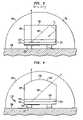
- FIG. 8shows a LED package 510 , in accordance with further preferred embodiments of the present invention.
- the LED packageincludes LED 518 having first layer 520 , second layer 522 and junction 524 extending between first and second layer 520 , 522 .
- a substantially transparent substrate 526is formed atop second layer 522 of LED 518 .
- Substantially transparent substrate 526includes first surface 550 and second surface 552 remote therefrom.
- a grating pattern 554is formed atop second surface 552 of substrate 526 .
- the grating patternis preferably formed by an additive process that adds material to the second surface of the substrate 526 .
- the grating patternresults in light rays generated by LED 518 being reflected through sidewall 570 of substantially transparent substrate 526 .
- the pattern and/or spacing of the gratings 554is matched with the wavelength of the light emitted from junction 524 .
- the pattern of the grating 554is matched with the wavelength of the LED 518 so that an optimum amount of light is transmitted through the sidewall 570 of substrate 526 and through the sides of LED package 510 .
Landscapes
- Led Device Packages (AREA)
Abstract
Description
Claims (17)
Priority Applications (1)
| Application Number | Priority Date | Filing Date | Title |
|---|---|---|---|
| US10/416,996US7023022B2 (en) | 2000-11-16 | 2001-11-14 | Microelectronic package having improved light extraction |
Applications Claiming Priority (3)
| Application Number | Priority Date | Filing Date | Title |
|---|---|---|---|
| US24931100P | 2000-11-16 | 2000-11-16 | |
| US10/416,996US7023022B2 (en) | 2000-11-16 | 2001-11-14 | Microelectronic package having improved light extraction |
| PCT/US2001/044047WO2002041406A1 (en) | 2000-11-16 | 2001-11-14 | Microelectronic package having improved light extraction |
Publications (2)
| Publication Number | Publication Date |
|---|---|
| US20040065886A1 US20040065886A1 (en) | 2004-04-08 |
| US7023022B2true US7023022B2 (en) | 2006-04-04 |
Family
ID=22942928
Family Applications (1)
| Application Number | Title | Priority Date | Filing Date |
|---|---|---|---|
| US10/416,996Expired - Fee RelatedUS7023022B2 (en) | 2000-11-16 | 2001-11-14 | Microelectronic package having improved light extraction |
Country Status (3)
| Country | Link |
|---|---|
| US (1) | US7023022B2 (en) |
| AU (1) | AU2002217845A1 (en) |
| WO (1) | WO2002041406A1 (en) |
Cited By (19)
| Publication number | Priority date | Publication date | Assignee | Title |
|---|---|---|---|---|
| US20050056831A1 (en)* | 2003-09-17 | 2005-03-17 | Toyoda Gosei Co., Ltd. | Light-emitting device |
| US20060084191A1 (en)* | 2004-10-20 | 2006-04-20 | Lu-Chen Hwan | Packaging method for an electronic element |
| US20060261470A1 (en)* | 2005-04-05 | 2006-11-23 | Tir Systems Ltd. | Electronic device package with an integrated evaporator |
| US20080180960A1 (en)* | 2006-10-31 | 2008-07-31 | Shane Harrah | Lighting device package |
| US20080220342A1 (en)* | 2007-03-02 | 2008-09-11 | Micron Technology, Inc. | Methods of fabricating optical packages, systems comprising the same, and their uses |
| US20080296589A1 (en)* | 2005-03-24 | 2008-12-04 | Ingo Speier | Solid-State Lighting Device Package |
| US20090008662A1 (en)* | 2007-07-05 | 2009-01-08 | Ian Ashdown | Lighting device package |
| DE102007041852A1 (en)* | 2007-09-03 | 2009-03-05 | Osram Opto Semiconductors Gmbh | High power LED module, has semicircular hollow portion extending into transparent carrier on side of LED and having evaporable cooling agent, and electrode structures provided in transparent carrier |
| CN101226974B (en)* | 2007-01-18 | 2011-01-05 | 财团法人工业技术研究院 | Light emitting diode chip with micro-mirror structure |
| US7906794B2 (en) | 2006-07-05 | 2011-03-15 | Koninklijke Philips Electronics N.V. | Light emitting device package with frame and optically transmissive element |
| US7939832B2 (en) | 2007-03-08 | 2011-05-10 | Sensors For Medicine And Science, Inc. | Light emitting diode for harsh environments |
| WO2011143918A1 (en)* | 2010-11-03 | 2011-11-24 | 映瑞光电科技(上海)有限公司 | Light emitting diode and manufacturing method thereof |
| US20120074443A1 (en)* | 2010-09-29 | 2012-03-29 | Forward Electronics Co., Ltd. | LED package structure |
| US8178892B2 (en) | 2005-08-04 | 2012-05-15 | Industrial Technology Research Institute | LED chip having micro-lens structure |
| US8405063B2 (en) | 2007-07-23 | 2013-03-26 | Qd Vision, Inc. | Quantum dot light enhancement substrate and lighting device including same |
| US9543490B2 (en) | 2010-09-24 | 2017-01-10 | Seoul Semiconductor Co., Ltd. | Wafer-level light emitting diode package and method of fabricating the same |
| US10006615B2 (en) | 2014-05-30 | 2018-06-26 | Oelo, LLC | Lighting system and method of use |
| US10580929B2 (en) | 2016-03-30 | 2020-03-03 | Seoul Viosys Co., Ltd. | UV light emitting diode package and light emitting diode module having the same |
| US11757074B2 (en) | 2020-06-12 | 2023-09-12 | Apple Inc. | Light-emitting diode display pixels with microlens stacks over light-emitting diodes |
Families Citing this family (49)
| Publication number | Priority date | Publication date | Assignee | Title |
|---|---|---|---|---|
| US6878969B2 (en)* | 2002-07-29 | 2005-04-12 | Matsushita Electric Works, Ltd. | Light emitting device |
| DE10234977A1 (en)* | 2002-07-31 | 2004-02-12 | Osram Opto Semiconductors Gmbh | Radiation-emitting thin layer semiconductor component comprises a multiple layer structure based on gallium nitride containing an active radiation-producing layer and having a first main surface and a second main surface |
| KR100499129B1 (en)* | 2002-09-02 | 2005-07-04 | 삼성전기주식회사 | Light emitting laser diode and fabricatin method thereof |
| US7074631B2 (en) | 2003-04-15 | 2006-07-11 | Luminus Devices, Inc. | Light emitting device methods |
| US7084434B2 (en) | 2003-04-15 | 2006-08-01 | Luminus Devices, Inc. | Uniform color phosphor-coated light-emitting diode |
| US7098589B2 (en) | 2003-04-15 | 2006-08-29 | Luminus Devices, Inc. | Light emitting devices with high light collimation |
| US6831302B2 (en) | 2003-04-15 | 2004-12-14 | Luminus Devices, Inc. | Light emitting devices with improved extraction efficiency |
| US7521854B2 (en) | 2003-04-15 | 2009-04-21 | Luminus Devices, Inc. | Patterned light emitting devices and extraction efficiencies related to the same |
| US7211831B2 (en) | 2003-04-15 | 2007-05-01 | Luminus Devices, Inc. | Light emitting device with patterned surfaces |
| US7262550B2 (en) | 2003-04-15 | 2007-08-28 | Luminus Devices, Inc. | Light emitting diode utilizing a physical pattern |
| US20040259279A1 (en) | 2003-04-15 | 2004-12-23 | Erchak Alexei A. | Light emitting device methods |
| US7105861B2 (en) | 2003-04-15 | 2006-09-12 | Luminus Devices, Inc. | Electronic device contact structures |
| US7083993B2 (en) | 2003-04-15 | 2006-08-01 | Luminus Devices, Inc. | Methods of making multi-layer light emitting devices |
| US7274043B2 (en) | 2003-04-15 | 2007-09-25 | Luminus Devices, Inc. | Light emitting diode systems |
| US7193784B2 (en)* | 2003-05-20 | 2007-03-20 | Kansas State University Research Foundation | Nitride microlens |
| CN100383639C (en)* | 2003-09-06 | 2008-04-23 | 鸿富锦精密工业(深圳)有限公司 | Back-to-light module |
| US7341880B2 (en)* | 2003-09-17 | 2008-03-11 | Luminus Devices, Inc. | Light emitting device processes |
| US7344903B2 (en) | 2003-09-17 | 2008-03-18 | Luminus Devices, Inc. | Light emitting device processes |
| CN100383637C (en)* | 2003-09-26 | 2008-04-23 | 鸿富锦精密工业(深圳)有限公司 | LED light source and backlight module |
| JP4881003B2 (en) | 2003-09-26 | 2012-02-22 | オスラム オプト セミコンダクターズ ゲゼルシャフト ミット ベシュレンクテル ハフツング | Thin film semiconductor chip that emits radiation |
| US7450311B2 (en) | 2003-12-12 | 2008-11-11 | Luminus Devices, Inc. | Optical display systems and methods |
| EP1705764B1 (en)* | 2004-01-07 | 2012-11-14 | Hamamatsu Photonics K. K. | Semiconductor light-emitting device and its manufacturing method |
| JP4116587B2 (en) | 2004-04-13 | 2008-07-09 | 浜松ホトニクス株式会社 | Semiconductor light emitting device and manufacturing method thereof |
| JP4397728B2 (en)* | 2004-04-21 | 2010-01-13 | 日東電工株式会社 | Direct type backlight |
| US7361938B2 (en)* | 2004-06-03 | 2008-04-22 | Philips Lumileds Lighting Company Llc | Luminescent ceramic for a light emitting device |
| US20090023239A1 (en)* | 2004-07-22 | 2009-01-22 | Luminus Devices, Inc. | Light emitting device processes |
| JP2006100787A (en) | 2004-08-31 | 2006-04-13 | Toyoda Gosei Co Ltd | Light emitting device and light emitting element |
| GB2417825B (en)* | 2004-09-04 | 2006-11-22 | Arima Optoelectronics Corp | Light emitting diode with diffraction lattice |
| JP2006324324A (en)* | 2005-05-17 | 2006-11-30 | Sumitomo Electric Ind Ltd | Light emitting device, method for manufacturing light emitting device, and nitride semiconductor substrate |
| US7348603B2 (en) | 2005-10-17 | 2008-03-25 | Luminus Devices, Inc. | Anisotropic collimation devices and related methods |
| US7391059B2 (en) | 2005-10-17 | 2008-06-24 | Luminus Devices, Inc. | Isotropic collimation devices and related methods |
| US7388233B2 (en) | 2005-10-17 | 2008-06-17 | Luminus Devices, Inc. | Patchwork patterned devices and related methods |
| US7375379B2 (en)* | 2005-12-19 | 2008-05-20 | Philips Limileds Lighting Company, Llc | Light-emitting device |
| US7682850B2 (en)* | 2006-03-17 | 2010-03-23 | Philips Lumileds Lighting Company, Llc | White LED for backlight with phosphor plates |
| US8080828B2 (en)* | 2006-06-09 | 2011-12-20 | Philips Lumileds Lighting Company, Llc | Low profile side emitting LED with window layer and phosphor layer |
| US7626210B2 (en)* | 2006-06-09 | 2009-12-01 | Philips Lumileds Lighting Company, Llc | Low profile side emitting LED |
| US20080121902A1 (en)* | 2006-09-07 | 2008-05-29 | Gelcore Llc | Small footprint high power light emitting package with plurality of light emitting diode chips |
| US8110838B2 (en) | 2006-12-08 | 2012-02-07 | Luminus Devices, Inc. | Spatial localization of light-generating portions in LEDs |
| DE102007019776A1 (en)* | 2007-04-26 | 2008-10-30 | Osram Opto Semiconductors Gmbh | Optoelectronic component and method for producing a plurality of optoelectronic components |
| US9046634B2 (en)* | 2007-06-14 | 2015-06-02 | Philips Lumileds Lighting Company, Llc | Thin flash or video recording light using low profile side emitting LED |
| DE102007058453A1 (en)* | 2007-09-10 | 2009-03-12 | Osram Opto Semiconductors Gmbh | Radiation-emitting device |
| WO2014108782A1 (en) | 2013-01-09 | 2014-07-17 | Koninklijke Philips N.V. | Shaped cavity in substrate of a chip scale package led |
| US20150340566A1 (en)* | 2013-01-10 | 2015-11-26 | Koninklijke Philips N.V. | Led with shaped growth substrate for side emission |
| JP6506899B2 (en)* | 2015-10-08 | 2019-04-24 | 日亜化学工業株式会社 | Light emitting device, integrated light emitting device and light emitting module |
| WO2017061127A1 (en) | 2015-10-08 | 2017-04-13 | Nichia Corporation | Light-emitting device, integrated light-emitting device, and light-emitting module |
| US11430919B2 (en)* | 2019-04-26 | 2022-08-30 | Lumileds Llc | High brightness LEDs with non-specular nanostructured thin film reflectors |
| CN112968092A (en)* | 2020-11-19 | 2021-06-15 | 重庆康佳光电技术研究院有限公司 | Light emitting device, manufacturing method thereof and display panel with light emitting device |
| CN113644058B (en)* | 2021-08-11 | 2022-06-28 | 福建兆元光电有限公司 | A backlight type Mini LED chip and its manufacturing method |
| WO2024240564A1 (en)* | 2023-05-25 | 2024-11-28 | Ams-Osram International Gmbh | Optoelectronic semiconductor chip and corresponding production method |
Citations (8)
| Publication number | Priority date | Publication date | Assignee | Title |
|---|---|---|---|---|
| EP0107480A2 (en) | 1982-10-21 | 1984-05-02 | Idec Izumi Corporation | Light emission diode lamp and method of producing it |
| JPH0316279A (en)* | 1989-06-14 | 1991-01-24 | Hitachi Ltd | Light emitting diode element and its manufacturing method |
| US5689279A (en) | 1994-03-24 | 1997-11-18 | Motorola | Integrated electro-optical package |
| US5779924A (en)* | 1996-03-22 | 1998-07-14 | Hewlett-Packard Company | Ordered interface texturing for a light emitting device |
| US6034424A (en) | 1996-07-31 | 2000-03-07 | Sumitomo Electric Industries, Ltd. | Package and optoelectronic device |
| US6274890B1 (en) | 1997-01-15 | 2001-08-14 | Kabushiki Kaisha Toshiba | Semiconductor light emitting device and its manufacturing method |
| US6278136B1 (en)* | 1997-04-22 | 2001-08-21 | Kabushiki Kaisha Toshiba | Semiconductor light emitting element, its manufacturing method and light emitting device |
| US6310364B1 (en)* | 1998-08-03 | 2001-10-30 | Toyoda Gosei Co., Ltd. | Light-emitting apparatus |
- 2001
- 2001-11-14WOPCT/US2001/044047patent/WO2002041406A1/ennot_activeApplication Discontinuation
- 2001-11-14AUAU2002217845Apatent/AU2002217845A1/ennot_activeAbandoned
- 2001-11-14USUS10/416,996patent/US7023022B2/ennot_activeExpired - Fee Related
Patent Citations (8)
| Publication number | Priority date | Publication date | Assignee | Title |
|---|---|---|---|---|
| EP0107480A2 (en) | 1982-10-21 | 1984-05-02 | Idec Izumi Corporation | Light emission diode lamp and method of producing it |
| JPH0316279A (en)* | 1989-06-14 | 1991-01-24 | Hitachi Ltd | Light emitting diode element and its manufacturing method |
| US5689279A (en) | 1994-03-24 | 1997-11-18 | Motorola | Integrated electro-optical package |
| US5779924A (en)* | 1996-03-22 | 1998-07-14 | Hewlett-Packard Company | Ordered interface texturing for a light emitting device |
| US6034424A (en) | 1996-07-31 | 2000-03-07 | Sumitomo Electric Industries, Ltd. | Package and optoelectronic device |
| US6274890B1 (en) | 1997-01-15 | 2001-08-14 | Kabushiki Kaisha Toshiba | Semiconductor light emitting device and its manufacturing method |
| US6278136B1 (en)* | 1997-04-22 | 2001-08-21 | Kabushiki Kaisha Toshiba | Semiconductor light emitting element, its manufacturing method and light emitting device |
| US6310364B1 (en)* | 1998-08-03 | 2001-10-30 | Toyoda Gosei Co., Ltd. | Light-emitting apparatus |
Cited By (36)
| Publication number | Priority date | Publication date | Assignee | Title |
|---|---|---|---|---|
| US7253450B2 (en)* | 2003-09-17 | 2007-08-07 | Toyoda Gosei Co., Ltd. | Light-emitting device |
| US20050056831A1 (en)* | 2003-09-17 | 2005-03-17 | Toyoda Gosei Co., Ltd. | Light-emitting device |
| US20060084191A1 (en)* | 2004-10-20 | 2006-04-20 | Lu-Chen Hwan | Packaging method for an electronic element |
| US7459345B2 (en)* | 2004-10-20 | 2008-12-02 | Mutual-Pak Technology Co., Ltd. | Packaging method for an electronic element |
| US20080296589A1 (en)* | 2005-03-24 | 2008-12-04 | Ingo Speier | Solid-State Lighting Device Package |
| US7505268B2 (en) | 2005-04-05 | 2009-03-17 | Tir Technology Lp | Electronic device package with an integrated evaporator |
| US20060261470A1 (en)* | 2005-04-05 | 2006-11-23 | Tir Systems Ltd. | Electronic device package with an integrated evaporator |
| US8178892B2 (en) | 2005-08-04 | 2012-05-15 | Industrial Technology Research Institute | LED chip having micro-lens structure |
| US7906794B2 (en) | 2006-07-05 | 2011-03-15 | Koninklijke Philips Electronics N.V. | Light emitting device package with frame and optically transmissive element |
| US20080180960A1 (en)* | 2006-10-31 | 2008-07-31 | Shane Harrah | Lighting device package |
| US7631986B2 (en) | 2006-10-31 | 2009-12-15 | Koninklijke Philips Electronics, N.V. | Lighting device package |
| CN101226974B (en)* | 2007-01-18 | 2011-01-05 | 财团法人工业技术研究院 | Light emitting diode chip with micro-mirror structure |
| US20090090924A1 (en)* | 2007-03-02 | 2009-04-09 | Klein Dean A | Intermediate optical packages and systems comprising the same, and their uses |
| US7732883B2 (en) | 2007-03-02 | 2010-06-08 | Aptina Imaging Corp. | Intermediate optical packages and systems comprising the same, and their uses |
| US7446385B2 (en)* | 2007-03-02 | 2008-11-04 | Micron Technology, Inc. | Methods of fabricating optical packages, systems comprising the same, and their uses |
| US20080220342A1 (en)* | 2007-03-02 | 2008-09-11 | Micron Technology, Inc. | Methods of fabricating optical packages, systems comprising the same, and their uses |
| US7939832B2 (en) | 2007-03-08 | 2011-05-10 | Sensors For Medicine And Science, Inc. | Light emitting diode for harsh environments |
| US8648356B2 (en) | 2007-03-08 | 2014-02-11 | Senseonics, Incorporated | Light emitting diode for harsh environments |
| US8415184B2 (en) | 2007-03-08 | 2013-04-09 | Sensors For Medicine And Science, Inc. | Light emitting diode for harsh environments |
| US20090008662A1 (en)* | 2007-07-05 | 2009-01-08 | Ian Ashdown | Lighting device package |
| US9680054B2 (en) | 2007-07-23 | 2017-06-13 | Samsung Electronics Co., Ltd. | Quantum dot light enhancement substrate and lighting device including same |
| US9276168B2 (en) | 2007-07-23 | 2016-03-01 | Qd Vision, Inc. | Quantum dot light enhancement substrate and lighting device including same |
| US10096744B2 (en) | 2007-07-23 | 2018-10-09 | Samsung Electronics Co., Ltd. | Quantum dot light enhancement substrate and lighting device including same |
| US8405063B2 (en) | 2007-07-23 | 2013-03-26 | Qd Vision, Inc. | Quantum dot light enhancement substrate and lighting device including same |
| US8759850B2 (en)* | 2007-07-23 | 2014-06-24 | Qd Vision, Inc. | Quantum dot light enhancement substrate |
| DE102007041852A1 (en)* | 2007-09-03 | 2009-03-05 | Osram Opto Semiconductors Gmbh | High power LED module, has semicircular hollow portion extending into transparent carrier on side of LED and having evaporable cooling agent, and electrode structures provided in transparent carrier |
| US9543490B2 (en) | 2010-09-24 | 2017-01-10 | Seoul Semiconductor Co., Ltd. | Wafer-level light emitting diode package and method of fabricating the same |
| US9882102B2 (en) | 2010-09-24 | 2018-01-30 | Seoul Semiconductor Co., Ltd. | Wafer-level light emitting diode and wafer-level light emitting diode package |
| US10069048B2 (en) | 2010-09-24 | 2018-09-04 | Seoul Viosys Co., Ltd. | Wafer-level light emitting diode package and method of fabricating the same |
| US10879437B2 (en) | 2010-09-24 | 2020-12-29 | Seoul Semiconductor Co., Ltd. | Wafer-level light emitting diode package and method of fabricating the same |
| US10892386B2 (en) | 2010-09-24 | 2021-01-12 | Seoul Semiconductor Co., Ltd. | Wafer-level light emitting diode package and method of fabricating the same |
| US20120074443A1 (en)* | 2010-09-29 | 2012-03-29 | Forward Electronics Co., Ltd. | LED package structure |
| WO2011143918A1 (en)* | 2010-11-03 | 2011-11-24 | 映瑞光电科技(上海)有限公司 | Light emitting diode and manufacturing method thereof |
| US10006615B2 (en) | 2014-05-30 | 2018-06-26 | Oelo, LLC | Lighting system and method of use |
| US10580929B2 (en) | 2016-03-30 | 2020-03-03 | Seoul Viosys Co., Ltd. | UV light emitting diode package and light emitting diode module having the same |
| US11757074B2 (en) | 2020-06-12 | 2023-09-12 | Apple Inc. | Light-emitting diode display pixels with microlens stacks over light-emitting diodes |
Also Published As
| Publication number | Publication date |
|---|---|
| AU2002217845A1 (en) | 2002-05-27 |
| WO2002041406A1 (en) | 2002-05-23 |
| US20040065886A1 (en) | 2004-04-08 |
Similar Documents
| Publication | Publication Date | Title |
|---|---|---|
| US7023022B2 (en) | Microelectronic package having improved light extraction | |
| US7015516B2 (en) | Led packages having improved light extraction | |
| US10573786B2 (en) | Semiconductor light emitting device | |
| US6921929B2 (en) | Light-emitting diode (LED) with amorphous fluoropolymer encapsulant and lens | |
| US6903379B2 (en) | GaN based LED lighting extraction efficiency using digital diffractive phase grating | |
| US10658546B2 (en) | High efficiency LEDs and methods of manufacturing | |
| US20040041164A1 (en) | Enhanced light extraction in leds through the use of internal and external optical elements | |
| US20040089868A1 (en) | Gallium nitride based compound semiconductor light-emitting device and manufacturing method therefor | |
| US12413884B2 (en) | Contact structures of LED chips for current injection | |
| US20110198564A1 (en) | Light emitting device and light emitting device package | |
| US7078252B2 (en) | Method of making group III nitride compound semiconductor light emitting element | |
| KR20020082143A (en) | Semiconductor light-emitting device | |
| CN108963051A (en) | Light emission diode package member | |
| EP2355183B1 (en) | Light emitting diode | |
| KR102175320B1 (en) | Light emitting device and lighting system having the same | |
| KR102851979B1 (en) | Light emitting device package | |
| KR20150047844A (en) | Semiconductor light emitting diode | |
| KR101956048B1 (en) | Light emitting device | |
| EP3103143B1 (en) | Light emitting diode with structured substrate | |
| EP4476775A1 (en) | Contact structures of led chips for current injection | |
| US20170170369A1 (en) | Surface mountable light emitting diode devices | |
| KR101672878B1 (en) | Semiconductor light emitting diode | |
| KR20150099696A (en) | Semiconductor light emitting diode | |
| WO2002059983A1 (en) | Led package having improved light extraction and methods therefor | |
| KR100905859B1 (en) | Nitride semiconductor light emitting device and manufacturing method thereof |
Legal Events
| Date | Code | Title | Description |
|---|---|---|---|
| AS | Assignment | Owner name:EMCORE CORPORATION, NEW JERSEY Free format text:ASSIGNMENT OF ASSIGNORS INTEREST;ASSIGNORS:ELIASHEVICH, IVAN;KARLICEK, ROBERT F. JR.;VENUGOPALAN, HARI;REEL/FRAME:014730/0249;SIGNING DATES FROM 20030723 TO 20030724 | |
| AS | Assignment | Owner name:BANK OF AMERICA, N.A., ILLINOIS Free format text:SECURITY AGREEMENT;ASSIGNOR:EMCORE CORPORATION;REEL/FRAME:021824/0019 Effective date:20080926 Owner name:BANK OF AMERICA, N.A.,ILLINOIS Free format text:SECURITY AGREEMENT;ASSIGNOR:EMCORE CORPORATION;REEL/FRAME:021824/0019 Effective date:20080926 | |
| FPAY | Fee payment | Year of fee payment:4 | |
| AS | Assignment | Owner name:WELLS FARGO BANK, NATIONAL ASSOCIATION, ARIZONA Free format text:SECURITY AGREEMENT;ASSIGNORS:EMCORE CORPORATION;EMCORE SOLAR POWER, INC.;REEL/FRAME:026304/0142 Effective date:20101111 | |
| AS | Assignment | Owner name:EMCORE CORPORATION, NEW MEXICO Free format text:RELEASE BY SECURED PARTY;ASSIGNOR:BANK OF AMERICA, N.A.;REEL/FRAME:027050/0880 Effective date:20110831 Owner name:EMCORE SOLAR POWER, INC., NEW MEXICO Free format text:RELEASE BY SECURED PARTY;ASSIGNOR:BANK OF AMERICA, N.A.;REEL/FRAME:027050/0880 Effective date:20110831 | |
| FPAY | Fee payment | Year of fee payment:8 | |
| FEPP | Fee payment procedure | Free format text:PAT HOLDER CLAIMS SMALL ENTITY STATUS, ENTITY STATUS SET TO SMALL (ORIGINAL EVENT CODE: LTOS); ENTITY STATUS OF PATENT OWNER: SMALL ENTITY | |
| FEPP | Fee payment procedure | Free format text:MAINTENANCE FEE REMINDER MAILED (ORIGINAL EVENT CODE: REM.) | |
| LAPS | Lapse for failure to pay maintenance fees | Free format text:PATENT EXPIRED FOR FAILURE TO PAY MAINTENANCE FEES (ORIGINAL EVENT CODE: EXP.) | |
| STCH | Information on status: patent discontinuation | Free format text:PATENT EXPIRED DUE TO NONPAYMENT OF MAINTENANCE FEES UNDER 37 CFR 1.362 | |
| FP | Lapsed due to failure to pay maintenance fee | Effective date:20180404 | |
| AS | Assignment | Owner name:EMCORE SOLAR POWER, INC., CALIFORNIA Free format text:RELEASE BY SECURED PARTY;ASSIGNOR:WELLS FARGO BANK;REEL/FRAME:061212/0728 Effective date:20220812 Owner name:EMCORE CORPORATION, CALIFORNIA Free format text:RELEASE BY SECURED PARTY;ASSIGNOR:WELLS FARGO BANK;REEL/FRAME:061212/0728 Effective date:20220812 |