US7022199B2 - Method for fabricating LCD - Google Patents
Method for fabricating LCDDownload PDFInfo
- Publication number
- US7022199B2 US7022199B2US10/184,083US18408302AUS7022199B2US 7022199 B2US7022199 B2US 7022199B2US 18408302 AUS18408302 AUS 18408302AUS 7022199 B2US7022199 B2US 7022199B2
- Authority
- US
- United States
- Prior art keywords
- substrate
- substrates
- aligning
- glass substrate
- alignment marks
- Prior art date
- Legal status (The legal status is an assumption and is not a legal conclusion. Google has not performed a legal analysis and makes no representation as to the accuracy of the status listed.)
- Expired - Lifetime, expires
Links
Images


Classifications
- G—PHYSICS
- G02—OPTICS
- G02F—OPTICAL DEVICES OR ARRANGEMENTS FOR THE CONTROL OF LIGHT BY MODIFICATION OF THE OPTICAL PROPERTIES OF THE MEDIA OF THE ELEMENTS INVOLVED THEREIN; NON-LINEAR OPTICS; FREQUENCY-CHANGING OF LIGHT; OPTICAL LOGIC ELEMENTS; OPTICAL ANALOGUE/DIGITAL CONVERTERS
- G02F1/00—Devices or arrangements for the control of the intensity, colour, phase, polarisation or direction of light arriving from an independent light source, e.g. switching, gating or modulating; Non-linear optics
- G02F1/01—Devices or arrangements for the control of the intensity, colour, phase, polarisation or direction of light arriving from an independent light source, e.g. switching, gating or modulating; Non-linear optics for the control of the intensity, phase, polarisation or colour
- G02F1/13—Devices or arrangements for the control of the intensity, colour, phase, polarisation or direction of light arriving from an independent light source, e.g. switching, gating or modulating; Non-linear optics for the control of the intensity, phase, polarisation or colour based on liquid crystals, e.g. single liquid crystal display cells
- G02F1/133—Constructional arrangements; Operation of liquid crystal cells; Circuit arrangements
- G02F1/1333—Constructional arrangements; Manufacturing methods
- G02F1/1341—Filling or closing of cells
- G—PHYSICS
- G02—OPTICS
- G02F—OPTICAL DEVICES OR ARRANGEMENTS FOR THE CONTROL OF LIGHT BY MODIFICATION OF THE OPTICAL PROPERTIES OF THE MEDIA OF THE ELEMENTS INVOLVED THEREIN; NON-LINEAR OPTICS; FREQUENCY-CHANGING OF LIGHT; OPTICAL LOGIC ELEMENTS; OPTICAL ANALOGUE/DIGITAL CONVERTERS
- G02F1/00—Devices or arrangements for the control of the intensity, colour, phase, polarisation or direction of light arriving from an independent light source, e.g. switching, gating or modulating; Non-linear optics
- G02F1/01—Devices or arrangements for the control of the intensity, colour, phase, polarisation or direction of light arriving from an independent light source, e.g. switching, gating or modulating; Non-linear optics for the control of the intensity, phase, polarisation or colour
- G02F1/13—Devices or arrangements for the control of the intensity, colour, phase, polarisation or direction of light arriving from an independent light source, e.g. switching, gating or modulating; Non-linear optics for the control of the intensity, phase, polarisation or colour based on liquid crystals, e.g. single liquid crystal display cells
- G02F1/133—Constructional arrangements; Operation of liquid crystal cells; Circuit arrangements
- G02F1/1333—Constructional arrangements; Manufacturing methods
- G02F1/1339—Gaskets; Spacers; Sealing of cells
- G—PHYSICS
- G02—OPTICS
- G02F—OPTICAL DEVICES OR ARRANGEMENTS FOR THE CONTROL OF LIGHT BY MODIFICATION OF THE OPTICAL PROPERTIES OF THE MEDIA OF THE ELEMENTS INVOLVED THEREIN; NON-LINEAR OPTICS; FREQUENCY-CHANGING OF LIGHT; OPTICAL LOGIC ELEMENTS; OPTICAL ANALOGUE/DIGITAL CONVERTERS
- G02F1/00—Devices or arrangements for the control of the intensity, colour, phase, polarisation or direction of light arriving from an independent light source, e.g. switching, gating or modulating; Non-linear optics
- G02F1/01—Devices or arrangements for the control of the intensity, colour, phase, polarisation or direction of light arriving from an independent light source, e.g. switching, gating or modulating; Non-linear optics for the control of the intensity, phase, polarisation or colour
- G02F1/13—Devices or arrangements for the control of the intensity, colour, phase, polarisation or direction of light arriving from an independent light source, e.g. switching, gating or modulating; Non-linear optics for the control of the intensity, phase, polarisation or colour based on liquid crystals, e.g. single liquid crystal display cells
- G02F1/133—Constructional arrangements; Operation of liquid crystal cells; Circuit arrangements
- G02F1/1333—Constructional arrangements; Manufacturing methods
- G02F1/1341—Filling or closing of cells
- G02F1/13415—Drop filling process
Definitions
- the present inventionrelates to a liquid crystal display, and more particularly, to a method for fabricating an LCD incorporating a liquid crystal dispensing method.
- LCDliquid crystal display
- PDPplasma display panel
- ELDelectro luminescent display
- VFDvacuum fluorescent display
- LCDshave been used most widely as mobile displays while replacing the CRT (Cathode Ray Tube) because of features and advantages including excellent picture quality, light weight, thin profile, and low power consumption.
- CRTCathode Ray Tube
- LCDshave been developed for computer monitors and televisions to receive and display broadcasting signals.
- the key to developing the LCDlies on whether the LCD can implement a high quality picture, such as high resolution, high luminance, and large-sized screen while still maintaining lightweight, thin profile, and low power consumption.
- LCDsmay be provided with a liquid crystal panel for displaying a picture, and a driving part for applying a driving signal to the liquid crystal panel.
- the liquid crystal panelhas first and second glass substrates bonded together with a gap between the substrates.
- a liquid crystal layeris formed by injecting liquid crystal between the first and second glass substrates.
- the first glass substratethere are a plurality of gate lines arranged in a first direction at fixed intervals, a plurality of data lines arranged in a second direction perpendicular to the gate lines at fixed intervals, a plurality of pixel electrodes in respective pixel regions defined by the gate lines and the data lines arranged in a matrix, a plurality of thin film transistors switchable in response to a signal on the gate lines for transmission of a signal on the data line to the pixel electrodes.
- the second glass substrate(a color filter substrate) has a black matrix layer for shielding light from areas excluding the pixel regions, R, G, B color filter layer, and a common electrode for implementing a picture.
- first and second substrateshave a gap between them which is maintained by spacers and are bonded to one another by a sealant.
- the sealhas a liquid crystal injection inlet through which the liquid crystal is injected after the two substrates are bonded and sealed.
- the space between the bonded two substrates of each LCD panelis evacuated and the liquid crystal injection inlet is dipped in a liquid crystal bath, so that the liquid crystal is injected into the space by a capillary tube phenomenon. Once the liquid crystal is injected into the space between the two substrates, the liquid crystal injection inlet is sealed by the sealant.
- the related art method for fabricating an LCD having liquid crystal injected thereinhas the following problems.
- the related art methodhas a poor productivity because the dipping of the liquid crystal injection inlet in a liquid crystal bath while the space between the two substrates are maintained at a vacuum after the unit panels are cut into individual pieces for injection of the liquid crystal takes much time.
- the liquid crystal injection for a large LCDin particular, may cause imperfect filling of the liquid crystal in the panel, which may result in a defective panel.
- the complicated and lengthy fabrication processrequires the use of many liquid crystal injection devices, which occupies much space.
- a Japanese laid-open patent publication No. 2000-147528discloses the following liquid crystal dropping method.
- FIGS. 1A-1Fillustrate steps of a related art method for fabricating an LCD.
- UV sealant 1is coated on a first glass substrate 3 having a thin film transistor array formed thereon to a thickness of approximately 30 ⁇ m, and liquid crystal 2 is dropped on an interior of the sealant 1 , which is the thin film transistor array part. No liquid crystal injection inlet is provided in the sealant 1 .
- the first glass substrate 3is mounted on a table 4 in a vacuum container ‘C’ which is movable in a horizontal direction, and held by vacuum on the bottom surface of the first glass substrate 3 by a first plurality of vacuum holes 5 .
- the bottom surface of the second glass substrate 6 having a color filter array formed thereonis held by vacuum using a second plurality of vacuum holes 7 .
- the vacuum container ‘C’is closed and evacuated.
- the second glass substrate 7is moved downward in a vertical direction until a gap between the first substrate 3 and second glass substrate 6 is 1 mm.
- the table 4 with supporting first glass substrate 3 thereonis moved in a horizontal direction to pre-align the first and second glass substrates 3 and 6 with respect to each other.
- the second glass substrate 6is moved downward until the second glass substrate 6 comes into contact with the liquid crystal 2 or the sealant 1 .
- the table 4 with the first glass substrate 3 thereonis moved in a horizontal direction to align the first and second glass substrates 3 and 6 .
- the second glass substrate 6is moved further down until the second glass substrate 6 bonds with the first glass substrate 3 through the sealant 1 .
- the second glass substrate 6is pressed down further until the gap between the second glass substrate 6 and the first glass substrate 3 becomes 5 m.
- the pre-bonded first and second glass substrates 3 and 6are taken out of the vacuum container ‘C’, and a UV ray is directed to the sealant to set the sealant 1 , thereby completing the fabrication process.
- the sealant coating and liquid crystal dropping on the same substratelead to require much fabrication time period before the two substrates are bonded.
- the first substratecan not be cleaned at an ultrasonic cleaner (USC). Therefore, as the sealant that will bond the two substrates should not be removed undesirable particles also cannot be removed which may cause defective contact of the sealant in the bonding.
- USBultrasonic cleaner
- the orientation film on the second substratemay become damaged, thereby causing poor picture quality. Further, if the upper and lower stages are not level, the first and second substrates may not fully contact each other and scratch the opposite substrate, or make the sealant uneven.
- the present inventionis directed to a liquid crystal display (LCD) and a method for fabricating a liquid crystal display that substantially obviates one or more of the problems due to limitations and disadvantages of the related art.
- An advantage of the present inventionis the provision of a method for fabricating an LCD incorporating a liquid crystal dropping method that reduces the time required to fabricate an LCD and increases the efficiency, to improve productivity of the LCD fabrication.
- a method for fabricating an LCDincludes steps of loading a first substrate having liquid crystal dropped thereon and a second substrate having sealant coated thereon on a bonding chamber, aligning the first and second substrates, bonding the first and second substrates with a varied pressure applied thereto, and unloading the bonded first and second substrates.
- the step of loadingmay include the steps of holding the first and second substrates to lower and upper stages, respectively, in the bonding chamber, positioning a substrate receiver in the bonding chamber under the second substrate held to the upper stage, evacuating the bonding chamber, and electrostatically securing the first and second substrates to the lower and upper stages, respectively.
- the step of evacuatingmay include performing a first evacuation after the first and second substrates are held to the lower and upper stages, respectively, in the bonding chamber and then performing a second evacuation after the substrate receiver is positioned under and contacts the second substrate held to the upper stage.
- the step of aligningmay include the step of successively aligning rough marks and fine marks, wherein the aligning is performed by moving the lower stage and alignment of the rough and fine marks is determined using separate cameras.
- alignment of the rough and fine marksmay be made by focusing on a central region between the first and second glass substrates.
- alignment of the rough and fine marksmay be made by alternately focusing on marks formed on the first and second glass substrates.
- alignment of the rough marksmay be made by providing a 0.4 mm-0.9 mm gap between the first glass substrate and the second glass substrate and alignment of the fine marks may be made by providing a 0.1 mm-0.4 mm gap between the first glass substrate and the second glass substrate.
- alignment of the fine marksmay be made by bringing liquid crystal dispensed on the first glass substrate into contact with the second glass substrate. Additionally, a plurality of the rough and fine marks may be formed between panels and/or in a periphery of the substrate.
- the step of bondingmay include a step varying a pressure applied to the substrates at least twice.
- the step of unloadingmay include the steps of loading an unbonded first or second substrate to the upper or lower stage, and unloading the bonded substrates.
- the liquid crystalis dispensed, and the sealant is coated, on the first substrate.
- the method for fabricating the LCDmay further include a step of spreading liquid crystal toward the sealant before or after the unloading.
- FIGS. 1A-1Fschematically illustrate steps of a related art method for fabricating an LCD incorporating a liquid crystal dispensing method
- FIG. 2schematically illustrates a flow chart showing the steps of a method for fabricating an LCD in accordance with an embodiment of the present invention
- FIGS. 3A-3Gschematically illustrate steps of a method for fabricating an LCD in accordance with an embodiment of the present invention
- FIG. 4illustrates a flow chart showing the steps of bonding in accordance with an embodiment of the present invention
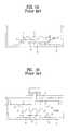
- FIGS. 5A-5Cillustrate an exemplary rough mark alignment method in accordance with an embodiment of the present invention
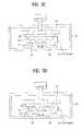
- FIGS. 6A-6Cillustrate an exemplary fine mark alignment method in accordance with an embodiment of the present invention
- FIG. 7illustrates a camera focusing position used in an alignment method in accordance with an embodiment of the present invention.
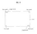
- FIG. 8illustrates an exemplary layout of rough and fine marks used in an alignment method in accordance with an embodiment of the present invention.
- FIG. 2schematically illustrates a flow chart showing the steps of a method for fabricating an LCD in accordance with an embodiment of the present invention while FIGS. 3A-3G schematically illustrate steps of a method for fabricating an LCD in accordance with an embodiment of the present invention.
- a plurality of panelsmay be designed on a first glass substrate 11 and a thin film transistor array is formed on each panel ( 11 S), and a first orientation or alignment film is formed on an entire surface of the first glass substrate 11 . Then a rubbing process ( 12 S) is performed. Instead of the rubbing process, a UV alignment process may be performed.
- a plurality of panelsare designed on a second glass substrate 13 corresponding to the panels on the first glass substrate 11 , to form a color filter array on each panel ( 15 S).
- the color filter arrayincludes such elements as a black matrix layer, a color filter layer, and a common electrode.
- a second orientation or alignment filmis formed on an entire surface of the second substrate 13 and the second orientation film undergoes a rubbing process ( 16 S) similar to the first orientation film.
- the first and second glass substrates 11 and 13 thus formedare cleaned, respectively ( 13 S and 17 S).
- liquid crystal 12is dispensed or applied to the first glass substrate 11 which has been cleaned ( 14 S).
- Silver (Ag) dotsare formed on the cleaned second glass substrate 13 ( 18 S), and a sealant 14 is coated thereon ( 19 S).
- the first and second glass substrates 11 and 13are loaded in a vacuum bonding chamber 10 , and bonded to spread the applied liquid crystal between the first and second substrates uniformly, and then, the sealant is hardened ( 20 S).
- the bonded first and second glass substrates 11 and 13are cut into a plurality of individual panels ( 21 S). Although a plurality of individual panels may be cut from any glass substrate, a single panel may also be formed to maximize the size of the display. Subsequently, each panel is then polished and inspected (S 22 ).
- FIG. 4illustrates a flowchart showing the bonding steps of the present invention.
- the bonding processmay include the steps of loading the two substrates into the vacuum bonding chamber, bonding the two substrates together, and unloading the bonded substrates from the vacuum bonding chamber.
- the second glass substrate 13 having the sealant 14 coated thereonmay be cleaned using, for example, an ultra sonic cleaner (USC) to remove undesirable contaminant particles formed during fabrication. Since the second glass substrate 13 is coated by the sealant and the Ag dots, and no liquid crystal has been dispensed thereon, the second glass substrate 13 may be cleaned.
- an ultra sonic cleanerUSC
- the second glass substrate 13 having the sealant 14 coated thereon and facing in a downward directionis held to an upper stage 15 by, for example, a vacuum or electrostatic chuck provided in the vacuum bonding chamber 10 ( 31 S).
- the second glass substrate 13may be flipped over so that the surface with the sealant 14 will face in a downward direction, as will be explained in greater detail below.
- a loader of a robotmay hold the substrate such that the sealant 14 is facing in a downward direction as it is brought in the vacuum bonding chamber 10 .
- the upper stage 15 in the vacuum bonding chamber 10may be moved vertically downward to contact and hold the second glass substrate 13 , and then may be moved vertically upward.
- the second glass substrate 13may be held to the upper stage 15 using a vacuum chuck, electrostatic charge (ESC), or any other suitable holding technique.
- ESCelectrostatic charge
- the loader of the robotis then moved out of the vacuum bonding chamber 10 and the first glass substrate 11 is arranged over the lower stage 16 by the loader of the robot.
- the sealantmay alternatively be coated on the first glass substrate 11 while the liquid crystal may alternatively be dispensed on the second substrate.
- the sealantmay be applied to both substrates.
- the liquid crystalmay be dispensed, or the sealant coated, on either of the two glass substrates as long as the substrate with the liquid crystal material dispensed thereon is located on the lower stage and the other substrate is located on the upper stage.
- the first and second substratesmay be aligned.
- a substrate receiver(not shown) is contacted with a bottom surface of the second glass substrate 13 ( 33 S) by positioning the substrate receiver under the second glass substrate 13 and moving the upper stage down, or the substrate receiver up, or both, until the second glass substrate 13 contacts the substrate receiver.
- the substrate receiveris positioned below the second glass substrate 13 , to prevent the second glass substrate held to the upper stage from becoming detached from the upper stage due to a reduction in a vacuum force present within the upper stage when the vacuum pressure in the bonding chamber becomes higher than the vacuum force within the upper and lower stages.
- the second glass substrate 13 , held to the upper stagemay be arranged on the substrate receiver before or during the creation of a vacuum in the vacuum bonding chamber.
- the upper stage holding the second glass substrate and the substrate receivermay be brought within a predetermined distance of each other so that the second glass substrate 13 may be safely arranged on the substrate receiver from the upper stage when the chamber is evacuated.
- means for fastening the substratesmay be provided additionally as air flow in the chamber, capable of shaking the substrates, may occur when evacuation of the vacuum bonding chamber is initiated.
- the vacuum within the vacuum bonding chamber 10may have a pressure in a first range of about 1.0 ⁇ 10 ⁇ 3 Pa to 1 Pa or a second range of about 1.1 ⁇ 10 ⁇ 3 Pa to 10 2 Pa.
- the first rangemay be especially applicable for an in-plane switching (IPS) mode LCD and the second range may be especially useful for a twisted nematic (TN) mode LCD.
- IPSin-plane switching
- TNtwisted nematic
- VAvertical alignment
- Evacuation of the vacuum bonding chamber 10may be carried out in two stages. After the substrates are held to their respective stages, a chamber door is closed and the vacuum chamber is evacuated a first time. After positioning the substrate receiver under the upper stage and placing the substrate on the substrate receiver or after positioning the upper stage and the substrate receiver to within the predetermined distance when the upper stage holds the substrate, the vacuum bonding chamber is evacuated a second time. The second evacuation is faster than the first evacuation and the vacuum pressure created by the first evacuation is not greater than the vacuum pressure created within the upper stage.
- the aforementioned two stage evacuation processmay prevent deformation or shaking of the substrates when the vacuum bonding chamber is rapidly evacuated.
- the evacuationmay be implemented in a single step at a fixed rate.
- the substrate receivermay be positioned below the second substrate 13 held to the upper stage 15 during the evacuation. Before the vacuum pressure in the vacuum bonding chamber becomes higher than the vacuum holding force of the upper stage it is required that the substrate receiver be in contact with the second glass substrate 13 .
- the first and second glass substrates 11 and 13are electrostatically secured to their respective stages using an electrostatic chuck (ESC) ( 35 S) and the substrate receiver may be brought to its original position ( 36 S). Accordingly, the loading process is completed.
- ESCelectrostatic chuck
- the first and second glass substratesmay be held to their respective stages by applying negative/positive DC voltages to two or more plate electrodes (not shown) formed within the stages.
- a coulombic forceis generated between a conductive layer (e.g., transparent electrodes, common electrodes, pixel electrodes, etc.) formed on the substrate and the stage.
- a conductive layere.g., transparent electrodes, common electrodes, pixel electrodes, etc.
- conductive layer formed on the substratefaces the stage, about 0.1-1 KV may be applied to the plate electrodes.
- the substratecontains no conductive layer, about 3-4 KV may be applied to the plate electrodes.
- An elastic sheetmay be optionally be provided to the upper stage.
- the first and second glass substrate 11 and 13are aligned ( 37 S) in an alignment method, as will be explained in greater detail below.
- FIGS. 5A-5Cillustrate an exemplary rough mark alignment method in accordance with an embodiment of the present invention
- FIGS. 6A-6Cillustrate a fine mark alignment method in accordance with an embodiment of the present invention
- FIG. 7illustrates a camera focusing position used in an alignment method in accordance with an embodiment of the present invention.
- the first glass substrate 11 and the second glass substrate 13include rough alignment marks measuring approximately 3 ⁇ m in size ( FIGS. 5A-5C ) and fine alignment marks measuring approximately 0.3 ⁇ m in size (FIGS. 6 A- 6 C).
- the first glass substrate 11includes a least one rough alignment mark as shown in FIG. 5 A and at least one fine alignment mark as shown in FIG. 6 A.
- the second glass substrate 13includes at least one rough alignment mark as shown in FIG. 5 B and at least one fine alignment mark as shown in FIG. 6 B.
- different camerasmay be used to align the rough marks and the fine marks.
- a single cameramay be used to align both the rough marks and the fine marks.
- the cameras used to align the rough and fine marksmay be focused on a central part between the first glass substrate 11 and the second glass substrate 13 .
- the upper stage 15is moved down a first time such that the second glass substrate 13 does not touch the liquid crystal dispensed on the first glass substrate and a gap between the first glass substrate 11 and the second glass substrate 13 is in a range of 0.4 mm-0.9 mm, for example 0.6 mm.
- the first glass substrate 11is roughly aligned with the second glass substrate 13 such that the rough marks on the second glass substrate 13 may be located within the rough marks on the first glass substrate 11 .
- an area of approximately 3.0 mmmay be searched in order to determine the positions of the rough and fine alignment marks.
- the upper stage 15is moved down a second time such that a gap between the first glass substrate 11 and the second glass substrate 13 is in a range of 0.1 mm-0.4 mm, for example, 0.2 mm.
- the first glass substrate 11is finely aligned with the second glass substrate 13 such that the fine mark on the second glass substrate 13 is accurately located within the fine mark on the first glass substrate 11 .
- an area of approximately 0.2 mmmay be searched in order to determine the positions of the rough and fine alignment marks.
- an alignment tolerance of approximately 0.1 ⁇ mmay be achieved as a result of aligning the first and second substrates.
- the liquid crystal 12 dispensed on the first glass substrate 11may contact the second glass substrate 13 .
- the lower stage 16may be moved horizontally to align the two substrates.
- the camerasmay be provided above or below the upper or lower surfaces of the first or second substrates.
- the cameras used to locate the alignment marksmay be positioned outside the vacuum bonding chamber. Accordingly, the cameras may be used to view rough and fine alignment marks on the first and second substrates through one or more windows provided in top and bottom walls of the vacuum chamber, as required.
- the windows, through which the alignment marks are viewed by the camerasmay be provided within recessed cavities formed in the top and bottom walls of the vacuum chamber. Accordingly, in the present aspect of the invention, a single camera may be used to view alignment marks formed on the upper and lower substrates by moving the cameras up and down within their respective cavities. Alternately, a single, stationary camera may be used to view alignment marks on a single substrate. Accordingly, movement of the cameras is not required.
- a central part between the alignment marks on the second glass substrate 13 and the alignment marks on the first glass substrate 11may be focused on using the cameras.
- a focal point of the camerasmay be adjusted to focus on alignment marks formed on the on the second glass substrate 13 and then to focus on alignment marks formed on the first glass substrate 11 , thereby improving an alignment accuracy over that of the aforementioned first example.
- FIG. 8illustrates an exemplary layout of rough and fine marks used in an alignment method in accordance with an embodiment of the present invention.
- At least four rough and fine marksmay be formed on the first and second glass substrates 11 and 13 .
- Alignment marks on one substratecorrespond in location to alignment marks formed on another substrate.
- the number of alignment marksmay be increased as the size of the glass substrate increases.
- the rough marks and the fine marksmay be formed in regions between panels which are to be cut, or in a periphery region of the substrate outside of where the plurality of panels are formed.
- FIGS. 5C and 6Cillustrate times the rough marks and the fine marks are aligned, and the first glass substrate 11 are aligned with the second glass substrate 13 by employing different cameras in alignment of the rough marks and the fine marks, the alignment can be made more faster and accurately.
- the upper stage 15is moved down and a pressure is applied to the first and second glass substrates 11 and 13 , thereby bonding the two substrates together ( 38 S).
- the first and second glass substrates 11 and 13are bonded together by moving either the upper stage 15 or the lower stage 16 in a vertical direction, while varying speeds and the pressures of the upper and lower stages.
- the stagesare moved at a fixed speed or fixed pressure. After the time of initial contact, the pressure is increased gradually from the fixed pressure to a final pressure.
- the two glass substrates 11 and 13may, for example, be pressed at a first pressure of 0.1 ton at the initial time of contact, a second pressure of 0.3 ton at a first intermediate stage, a third pressure of 0.4 ton at a second intermediate stage, and a fourth pressure of 0.5 ton at a final stage (see FIG. 3 F).
- a plurality of shaftsmay independently apply and control pressure using individual load cells fitted thereto. If the lower stage and the upper stage are not level or fail to be pressed uniformly, a predetermined number of shafts may be selectively activated to apply lower or higher pressures to the substrates, thereby providing uniform bonding of the sealant.
- the ESCis turned off and the upper stage 15 is raised upward and separates from the bonded glass substrates 11 and 13 .
- the bonded substratesare unloaded ( 39 S). Accordingly, after the upper stage is raised to a final raised position, the bonded glass substrates may be unloaded using the loader of the robot. Alternatively, the bonded glass substrates may be held by the upper stage during its ascent to its final raised position wherein the loader of the robot unloads the first and second glass substrates 11 and 13 from the upper stage 16 . The bonded substrates may be held to the upper stage by a vacuum or an electrostatic charge.
- an unbonded first glass substrate 11 or second glass substrate 13may be loaded onto a stage while the bonded substrates are unloaded from a stage. Accordingly, an unbonded second glass substrate 13 may be brought to the upper stage 15 by means of the loader of the robot and held to the upper stage by a vacuum or an electrostatic charge while the bonded first and second glass substrates may be unloaded from the lower stage 16 . Alternatively, an unbonded first glass substrate 11 may be brought to the lower stage 16 by means of the loader robot while the bonded first and second glass substrates held by the upper stage 15 may be unloaded.
- a liquid crystal spreading processmay be provided before or after the bonded substrates are unloaded. Accordingly, the liquid crystal spreading process spreads the liquid crystal in the gap between the bonded substrates toward the sealant in the event the liquid crystal does not spread sufficiently toward the sealant before unloading.
- the liquid crystal spreading processmay be carried out for at least 10 minutes under the atmospheric or a vacuum pressure.
- the method for fabricating LCDs of the present inventionhas the following advantages.
- applying the liquid crystal on the first substrate and coating the seal on the second substratepermits a balanced progression of the fabrication processes to the first and second substrates, thereby making efficient use of a production line.
- dispensing liquid crystal on the first substrate and coating the sealant and the Ag dots on the second substrateprevents the sealant from becoming contaminated with particles as the substrate coated by the sealant may be cleaned by a USC just prior to bonding.
- positioning the substrate receiver under the substrate and evacuation of the vacuum bonding chamberpermits the substrate held to the upper stage from falling and thereby breaking.
- the two staged evacuation of the vacuum bonding chamberprevents deformation of the substrate and air flow in the chamber caused by sudden pressure changes.
- the liquid crystal spreading processshortens a fabrication time period of the LCD.
Landscapes
- Physics & Mathematics (AREA)
- Nonlinear Science (AREA)
- Mathematical Physics (AREA)
- Chemical & Material Sciences (AREA)
- Crystallography & Structural Chemistry (AREA)
- General Physics & Mathematics (AREA)
- Optics & Photonics (AREA)
- Liquid Crystal (AREA)
- Container, Conveyance, Adherence, Positioning, Of Wafer (AREA)
Abstract
Description
Claims (21)
Applications Claiming Priority (3)
| Application Number | Priority Date | Filing Date | Title |
|---|---|---|---|
| KR2002-6656 | 2002-02-06 | ||
| KR10-2002-0006656AKR100469354B1 (en) | 2002-02-06 | 2002-02-06 | Method for manufacturing liquid crystal display device |
| KRP2002-6656 | 2002-02-06 |
Publications (2)
| Publication Number | Publication Date |
|---|---|
| US20030145944A1 US20030145944A1 (en) | 2003-08-07 |
| US7022199B2true US7022199B2 (en) | 2006-04-04 |
Family
ID=27656390
Family Applications (1)
| Application Number | Title | Priority Date | Filing Date |
|---|---|---|---|
| US10/184,083Expired - LifetimeUS7022199B2 (en) | 2002-02-06 | 2002-06-28 | Method for fabricating LCD |
Country Status (4)
| Country | Link |
|---|---|
| US (1) | US7022199B2 (en) |
| JP (1) | JP2003233078A (en) |
| KR (1) | KR100469354B1 (en) |
| CN (1) | CN1324377C (en) |
Cited By (8)
| Publication number | Priority date | Publication date | Assignee | Title |
|---|---|---|---|---|
| US20040089397A1 (en)* | 2002-10-25 | 2004-05-13 | Tung-Sheng Cheng | FPD encapsulation apparatus and method for encapsulating the same |
| US20050099574A1 (en)* | 2003-10-24 | 2005-05-12 | Nec Lcd Technologies, Ltd. | Liquid crystal display device and method for manufacturing the same |
| US20060021671A1 (en)* | 2004-07-28 | 2006-02-02 | Sharp Kabushiki Kaisha | Method and apparatus for fabricating liquid crystal display device and substrate base material for liquid crystal display device |
| US20060051887A1 (en)* | 2004-09-06 | 2006-03-09 | Fuji Photo Film Co., Ltd. | Manufacturing method and joining device for solid-state imaging devices |
| US20070151673A1 (en)* | 2005-12-29 | 2007-07-05 | Lg.Philips Lcd Co., Ltd. | Substrate bonding apparatus for liquid crystal display panel |
| US20080124199A1 (en)* | 2006-11-29 | 2008-05-29 | Jae Seok Hwang | Apparatus for attaching substrates |
| US20120171001A1 (en)* | 2010-12-29 | 2012-07-05 | Murata Manufacturing Co., Ltd. | Electronic component manufacturing apparatus and electronic component manufacturing method |
| US20140170924A1 (en)* | 2012-12-13 | 2014-06-19 | Chengdu Boe Optoelectronics Technology Co., Ltd. | Method for manufacturing a liquid crystal panel |
Families Citing this family (9)
| Publication number | Priority date | Publication date | Assignee | Title |
|---|---|---|---|---|
| KR100510724B1 (en)* | 2002-02-16 | 2005-08-30 | 엘지.필립스 엘시디 주식회사 | Method for manufacturing liquid crystal display device |
| KR100469359B1 (en)* | 2002-02-20 | 2005-02-02 | 엘지.필립스 엘시디 주식회사 | bonding device for liquid crystal display |
| KR100720449B1 (en)* | 2002-11-18 | 2007-05-22 | 엘지.필립스 엘시디 주식회사 | Liquid crystal display device manufacturing device |
| KR20070095371A (en)* | 2004-12-30 | 2007-09-28 | 이 아이 듀폰 디 네모아 앤드 캄파니 | Enclosure Tool and Method |
| KR101213874B1 (en)* | 2005-12-01 | 2012-12-18 | 엘지디스플레이 주식회사 | Liquid crystal display panel and repairing method thereof |
| US8173995B2 (en) | 2005-12-23 | 2012-05-08 | E. I. Du Pont De Nemours And Company | Electronic device including an organic active layer and process for forming the electronic device |
| US8617343B2 (en)* | 2009-12-25 | 2013-12-31 | Japan Display Central Inc. | Manufacturing method of flat-panel display device and bonding press apparatus therefor |
| US20140150952A1 (en)* | 2012-12-04 | 2014-06-05 | Apple Inc. | Lamination Systems With Temperature-Controlled Lamination Rollers |
| CN106019655A (en)* | 2016-07-26 | 2016-10-12 | 武汉华星光电技术有限公司 | Machine table |
Citations (168)
| Publication number | Priority date | Publication date | Assignee | Title |
|---|---|---|---|---|
| JPS5165656A (en) | 1974-12-04 | 1976-06-07 | Shinshu Seiki Kk | |
| US3978580A (en) | 1973-06-28 | 1976-09-07 | Hughes Aircraft Company | Method of fabricating a liquid crystal display |
| US4094058A (en) | 1976-07-23 | 1978-06-13 | Omron Tateisi Electronics Co. | Method of manufacture of liquid crystal displays |
| JPS5738414A (en) | 1980-08-20 | 1982-03-03 | Showa Denko Kk | Spacer for display panel |
| JPS5788428A (en) | 1980-11-20 | 1982-06-02 | Ricoh Elemex Corp | Manufacture of liquid crystal display body device |
| JPS5827126A (en) | 1981-08-11 | 1983-02-17 | Nec Corp | Production of liquid crystal display panel |
| JPS5957221A (en) | 1982-09-28 | 1984-04-02 | Asahi Glass Co Ltd | Production of display element |
| JPS59195222A (en) | 1983-04-19 | 1984-11-06 | Matsushita Electric Ind Co Ltd | Manufacture of liquid-crystal panel |
| JPS60111221A (en) | 1983-11-19 | 1985-06-17 | Nippon Denso Co Ltd | Method and device for charging liquid crystal |
| JPS60164723A (en) | 1984-02-07 | 1985-08-27 | Seiko Instr & Electronics Ltd | Liquid crystal display device |
| JPS60217343A (en) | 1984-04-13 | 1985-10-30 | Matsushita Electric Ind Co Ltd | Liquid crystal display device and its preparation |
| JPS617822A (en) | 1984-06-22 | 1986-01-14 | Canon Inc | Production of liquid crystal element |
| JPS6155625A (en) | 1984-08-24 | 1986-03-20 | Nippon Denso Co Ltd | Manufacture of liquid crystal element |
| US4653864A (en) | 1986-02-26 | 1987-03-31 | Ovonic Imaging Systems, Inc. | Liquid crystal matrix display having improved spacers and method of making same |
| JPS6289025A (en) | 1985-10-15 | 1987-04-23 | Matsushita Electric Ind Co Ltd | Manufacturing method of liquid crystal display panel |
| JPS6290622A (en) | 1985-10-17 | 1987-04-25 | Seiko Epson Corp | liquid crystal display device |
| US4691995A (en) | 1985-07-15 | 1987-09-08 | Semiconductor Energy Laboratory Co., Ltd. | Liquid crystal filling device |
| JPS62205319A (en) | 1986-03-06 | 1987-09-09 | Canon Inc | Ferroelectric liquid crystal element |
| JPS63109413A (en) | 1986-10-27 | 1988-05-14 | Fujitsu Ltd | Manufacturing method of LCD display |
| JPS63110425A (en) | 1986-10-29 | 1988-05-14 | Toppan Printing Co Ltd | Cell for liquid crystal filling |
| JPS63128315A (en) | 1986-11-19 | 1988-05-31 | Victor Co Of Japan Ltd | Liquid crystal display element |
| US4775225A (en) | 1985-05-16 | 1988-10-04 | Canon Kabushiki Kaisha | Liquid crystal device having pillar spacers with small base periphery width in direction perpendicular to orientation treatment |
| JPS63311233A (en) | 1987-06-12 | 1988-12-20 | Toyota Motor Corp | lcd cell |
| JPH05127179A (en) | 1991-11-01 | 1993-05-25 | Ricoh Co Ltd | Production of liquid crystal display element |
| JPH05154923A (en) | 1991-12-06 | 1993-06-22 | Hitachi Ltd | Substrate assembling device |
| US5247377A (en) | 1988-07-23 | 1993-09-21 | Rohm Gmbh Chemische Fabrik | Process for producing anisotropic liquid crystal layers on a substrate |
| JPH05265011A (en) | 1992-03-19 | 1993-10-15 | Seiko Instr Inc | Production of liquid crystal display element |
| JPH05281562A (en) | 1992-04-01 | 1993-10-29 | Matsushita Electric Ind Co Ltd | Manufacture of liquid crystal panel |
| JPH05281557A (en) | 1992-04-01 | 1993-10-29 | Matsushita Electric Ind Co Ltd | Liquid crystal panel manufacturing method |
| US5263888A (en)* | 1992-02-20 | 1993-11-23 | Matsushita Electric Industrial Co., Ltd. | Method of manufacture of liquid crystal display panel |
| JPH0651256A (en) | 1992-07-30 | 1994-02-25 | Matsushita Electric Ind Co Ltd | Device for discharging liquid crystal |
| JPH06148657A (en) | 1992-11-06 | 1994-05-27 | Matsushita Electric Ind Co Ltd | Method of manufacturing cell for liquid crystal display and manufacturing apparatus thereof |
| JPH06160871A (en) | 1992-11-26 | 1994-06-07 | Matsushita Electric Ind Co Ltd | Liquid crystal display panel and manufacturing method thereof |
| JPH06235925A (en) | 1993-02-10 | 1994-08-23 | Matsushita Electric Ind Co Ltd | Manufacture of liquid crystal display element |
| JPH06265915A (en) | 1993-03-12 | 1994-09-22 | Matsushita Electric Ind Co Ltd | Discharge device for filling liquid crystal |
| JPH06313870A (en) | 1993-04-28 | 1994-11-08 | Hitachi Ltd | Substrate assembly device |
| US5379139A (en) | 1986-08-20 | 1995-01-03 | Semiconductor Energy Laboratory Co., Ltd. | Liquid crystal device and method for manufacturing same with spacers formed by photolithography |
| JPH0784268A (en) | 1993-09-13 | 1995-03-31 | Hitachi Ltd | Sealing agent drawing method |
| US5406989A (en) | 1993-10-12 | 1995-04-18 | Ayumi Industry Co., Ltd. | Method and dispenser for filling liquid crystal into LCD cell |
| JPH07128674A (en) | 1993-11-05 | 1995-05-19 | Matsushita Electric Ind Co Ltd | Liquid crystal display element manufacturing method |
| JPH07181507A (en) | 1993-12-21 | 1995-07-21 | Canon Inc | Liquid crystal display device and information transmission device including the liquid crystal display device |
| US5464715A (en)* | 1993-04-02 | 1995-11-07 | Nikon Corporation | Method of driving mask stage and method of mask alignment |
| US5499128A (en) | 1993-03-15 | 1996-03-12 | Kabushiki Kaisha Toshiba | Liquid crystal display device with acrylic polymer spacers and method of manufacturing the same |
| JPH0895066A (en) | 1994-09-27 | 1996-04-12 | Matsushita Electric Ind Co Ltd | Method and apparatus for manufacturing liquid crystal element |
| JPH08101395A (en) | 1994-09-30 | 1996-04-16 | Matsushita Electric Ind Co Ltd | Liquid crystal display element manufacturing method |
| US5507323A (en) | 1993-10-12 | 1996-04-16 | Fujitsu Limited | Method and dispenser for filling liquid crystal into LCD cell |
| JPH08106101A (en) | 1994-10-06 | 1996-04-23 | Fujitsu Ltd | Liquid crystal display panel manufacturing method |
| JPH08171094A (en) | 1994-12-19 | 1996-07-02 | Nippon Soken Inc | Liquid crystal injecting method and liquid crystal injecting device to liquid crystal display device |
| JPH08190099A (en) | 1995-01-11 | 1996-07-23 | Fujitsu Ltd | Liquid crystal display device manufacturing method and liquid crystal display device manufacturing apparatus |
| US5539545A (en) | 1993-05-18 | 1996-07-23 | Semiconductor Energy Laboratory Co., Ltd. | Method of making LCD in which resin columns are cured and the liquid crystal is reoriented |
| US5548429A (en) | 1993-06-14 | 1996-08-20 | Canon Kabushiki Kaisha | Process for producing liquid crystal device whereby curing the sealant takes place after pre-baking the substrates |
| JPH08240807A (en) | 1995-03-06 | 1996-09-17 | Fujitsu Ltd | Liquid crystal display panel sealing method |
| JPH095762A (en) | 1995-06-20 | 1997-01-10 | Matsushita Electric Ind Co Ltd | Liquid crystal panel manufacturing method |
| JPH0926578A (en) | 1995-07-10 | 1997-01-28 | Fujitsu Ltd | Liquid crystal display panel and method of manufacturing the same |
| JPH0961829A (en) | 1995-08-21 | 1997-03-07 | Matsushita Electric Ind Co Ltd | Liquid crystal display element manufacturing method |
| JPH0973096A (en) | 1995-09-05 | 1997-03-18 | Matsushita Electric Ind Co Ltd | Liquid crystal display element manufacturing method |
| JPH0973075A (en) | 1995-09-05 | 1997-03-18 | Matsushita Electric Ind Co Ltd | Liquid crystal display element manufacturing method and liquid crystal display element manufacturing apparatus |
| JPH09127528A (en) | 1995-10-27 | 1997-05-16 | Fujitsu Ltd | Liquid crystal panel manufacturing method |
| US5642214A (en) | 1991-07-19 | 1997-06-24 | Sharp Kabushiki Kaisha | Optical modulating element and electronic apparatus using it |
| JPH09230357A (en) | 1996-02-22 | 1997-09-05 | Canon Inc | Liquid crystal panel manufacturing method and liquid crystal cell used therefor |
| JPH09281511A (en) | 1996-04-17 | 1997-10-31 | Fujitsu Ltd | Liquid crystal display panel manufacturing method |
| JPH09311340A (en) | 1996-05-21 | 1997-12-02 | Matsushita Electric Ind Co Ltd | Liquid crystal display manufacturing method |
| US5742370A (en) | 1996-09-12 | 1998-04-21 | Korea Institute Of Science And Technology | Fabrication method for liquid crystal alignment layer by magnetic field treatment |
| JPH10123538A (en) | 1996-10-22 | 1998-05-15 | Matsushita Electric Ind Co Ltd | Manufacturing method of liquid crystal display element |
| JPH10123537A (en) | 1996-10-15 | 1998-05-15 | Matsushita Electric Ind Co Ltd | Liquid crystal display device and method of manufacturing the same |
| US5757451A (en) | 1995-09-08 | 1998-05-26 | Kabushiki Kaisha Toshiba | Liquid crystal display device spacers formed from stacked color layers |
| JPH10142616A (en) | 1996-11-14 | 1998-05-29 | Ayumi Kogyo Kk | Liquid crystal injection method and liquid dispenser |
| JPH10177178A (en) | 1996-12-17 | 1998-06-30 | Matsushita Electric Ind Co Ltd | Manufacturing method of liquid crystal display element |
| JPH10221700A (en) | 1997-02-10 | 1998-08-21 | Fujitsu Ltd | Manufacturing method of liquid crystal display device |
| JPH10282512A (en) | 1997-04-07 | 1998-10-23 | Ayumi Kogyo Kk | Liquid crystal injection method and dispenser used therefor |
| JPH10333159A (en) | 1997-06-03 | 1998-12-18 | Matsushita Electric Ind Co Ltd | Liquid crystal display |
| JPH10333157A (en) | 1997-06-03 | 1998-12-18 | Matsushita Electric Ind Co Ltd | Manufacturing method of liquid crystal display device |
| US5852484A (en) | 1994-09-26 | 1998-12-22 | Matsushita Electric Industrial Co., Ltd. | Liquid crystal display panel and method and device for manufacturing the same |
| US5861932A (en) | 1997-03-31 | 1999-01-19 | Denso Corporation | Liquid crystal cell and its manufacturing method |
| JPH1114953A (en) | 1997-06-20 | 1999-01-22 | Matsushita Electric Ind Co Ltd | Method of manufacturing multi-touch liquid crystal display panel and multi-touch liquid crystal display panel |
| JPH1138424A (en) | 1997-07-23 | 1999-02-12 | Fujitsu Ltd | Liquid crystal display panel and method of manufacturing the same |
| US5875922A (en) | 1997-10-10 | 1999-03-02 | Nordson Corporation | Apparatus for dispensing an adhesive |
| JPH1164811A (en) | 1997-08-21 | 1999-03-05 | Matsushita Electric Ind Co Ltd | Method and apparatus for manufacturing liquid crystal display element |
| JPH11109388A (en) | 1997-10-03 | 1999-04-23 | Hitachi Ltd | Manufacturing method of liquid crystal display device |
| JPH11133438A (en) | 1997-10-24 | 1999-05-21 | Matsushita Electric Ind Co Ltd | Liquid crystal display device and its manufacturing method |
| JPH11142864A (en) | 1997-11-07 | 1999-05-28 | Matsushita Electric Ind Co Ltd | Manufacturing method of liquid crystal display device |
| JPH11174477A (en) | 1997-12-08 | 1999-07-02 | Matsushita Electric Ind Co Ltd | Manufacturing method of liquid crystal display device |
| JPH11212045A (en) | 1998-01-26 | 1999-08-06 | Matsushita Electric Ind Co Ltd | Liquid crystal panel manufacturing method |
| US5952678A (en) | 1995-01-23 | 1999-09-14 | Mitsubishi Denki Kabushiki Kaisha | SRAM cell with no PN junction between driver and load transistors and method of manufacturing the same |
| JPH11248930A (en) | 1998-03-06 | 1999-09-17 | Matsushita Electric Ind Co Ltd | Color filter substrate, method of manufacturing the color filter substrate, and liquid crystal display device using the color filter substrate |
| US5956112A (en) | 1995-10-02 | 1999-09-21 | Sharp Kabushiki Kaisha | Liquid crystal display device and method for manufacturing the same |
| JPH11326922A (en) | 1998-05-14 | 1999-11-26 | Matsushita Electric Ind Co Ltd | Liquid crystal display panel manufacturing method |
| US6001203A (en) | 1995-03-01 | 1999-12-14 | Matsushita Electric Industrial Co., Ltd. | Production process of liquid crystal display panel, seal material for liquid crystal cell and liquid crystal display |
| JPH11344714A (en) | 1998-06-02 | 1999-12-14 | Denso Corp | Liquid crystal cell |
| US6011609A (en) | 1996-10-05 | 2000-01-04 | Samsung Electronics Co., Ltd. | Method of manufacturing LCD by dropping liquid crystals on a substrate and then pressing the substrates |
| JP2000002879A (en) | 1998-06-12 | 2000-01-07 | Matsushita Electric Ind Co Ltd | Apparatus and method for assembling liquid crystal panel |
| US6016181A (en) | 1996-11-07 | 2000-01-18 | Sharp Kabushiki Kaisha | Liquid crystal device having column spacers with portion on each of the spacers for reflecting or absorbing visible light and method for fabricating the same |
| US6016178A (en) | 1996-09-13 | 2000-01-18 | Sony Corporation | Reflective guest-host liquid-crystal display device |
| JP2000029035A (en) | 1998-07-09 | 2000-01-28 | Minolta Co Ltd | Liquid crystal element and its manufacture |
| JP2000056311A (en) | 1998-08-03 | 2000-02-25 | Matsushita Electric Ind Co Ltd | Liquid crystal display |
| JP2000066165A (en) | 1998-08-20 | 2000-03-03 | Matsushita Electric Ind Co Ltd | Liquid crystal display panel manufacturing method |
| US6055035A (en) | 1998-05-11 | 2000-04-25 | International Business Machines Corporation | Method and apparatus for filling liquid crystal display (LCD) panels |
| JP2000137235A (en) | 1998-11-02 | 2000-05-16 | Matsushita Electric Ind Co Ltd | Liquid crystal substrate bonding method |
| EP1003066A1 (en) | 1998-11-16 | 2000-05-24 | Matsushita Electric Industrial Co., Ltd. | Method of manufacturing liquid crystal display devices |
| JP2000193988A (en) | 1998-12-25 | 2000-07-14 | Fujitsu Ltd | Method and apparatus for manufacturing liquid crystal display panel |
| JP2000241824A (en) | 1999-02-18 | 2000-09-08 | Matsushita Electric Ind Co Ltd | Manufacturing method of liquid crystal display device |
| JP2000284295A (en) | 1999-03-30 | 2000-10-13 | Hitachi Techno Eng Co Ltd | Substrate assembling method and apparatus |
| JP2000292799A (en) | 1999-04-09 | 2000-10-20 | Matsushita Electric Ind Co Ltd | Liquid crystal display device and method of manufacturing the same |
| JP2000310784A (en) | 1999-02-22 | 2000-11-07 | Matsushita Electric Ind Co Ltd | Liquid crystal panel, color filter and method for producing them |
| JP2000310759A (en) | 1999-04-28 | 2000-11-07 | Matsushita Electric Ind Co Ltd | Liquid crystal display device manufacturing apparatus and method |
| JP2000338501A (en) | 1999-05-26 | 2000-12-08 | Matsushita Electric Ind Co Ltd | Liquid crystal display panel manufacturing method |
| US6163357A (en) | 1996-09-26 | 2000-12-19 | Kabushiki Kaisha Toshiba | Liquid crystal display device having the driving circuit disposed in the seal area, with different spacer density in driving circuit area than display area |
| JP2001005405A (en) | 1999-06-18 | 2001-01-12 | Hitachi Techno Eng Co Ltd | Substrate assembling method and apparatus |
| JP2001005401A (en) | 1999-06-21 | 2001-01-12 | Hitachi Techno Eng Co Ltd | Substrate assembling method and apparatus |
| JP2001013506A (en) | 1999-04-30 | 2001-01-19 | Matsushita Electric Ind Co Ltd | Liquid crystal display device and method of manufacturing the same |
| JP2001033793A (en) | 1999-07-21 | 2001-02-09 | Matsushita Electric Ind Co Ltd | Liquid crystal display panel and method of manufacturing the same |
| JP2001042341A (en) | 1999-08-03 | 2001-02-16 | Hitachi Techno Eng Co Ltd | How to assemble a liquid crystal substrate |
| JP2001051284A (en) | 1999-08-10 | 2001-02-23 | Matsushita Electric Ind Co Ltd | Liquid crystal display device manufacturing equipment |
| JP2001066615A (en) | 2000-08-02 | 2001-03-16 | Matsushita Electric Ind Co Ltd | Manufacturing method of liquid crystal display device |
| JP2001091727A (en) | 1999-09-27 | 2001-04-06 | Matsushita Electric Ind Co Ltd | Method for manufacturing color filter substrate, color filter substrate and liquid crystal display device |
| US6219126B1 (en) | 1998-11-20 | 2001-04-17 | International Business Machines Corporation | Panel assembly for liquid crystal displays having a barrier fillet and an adhesive fillet in the periphery |
| US6222603B1 (en)* | 1998-01-13 | 2001-04-24 | Matsushita Electric Industrial Co., Ltd. | Method of manufacturing liquid crystal display device with a double seal |
| JP2001117109A (en) | 1999-10-21 | 2001-04-27 | Matsushita Electric Ind Co Ltd | Manufacturing method of liquid crystal display device |
| JP2001117105A (en) | 1999-10-18 | 2001-04-27 | Toshiba Corp | Manufacturing method of liquid crystal display device |
| US6226067B1 (en) | 1997-10-03 | 2001-05-01 | Minolta Co., Ltd. | Liquid crystal device having spacers and manufacturing method thereof |
| JP2001133745A (en) | 1999-11-08 | 2001-05-18 | Hitachi Techno Eng Co Ltd | Substrate assembling method and apparatus |
| JP2001133794A (en) | 1999-11-01 | 2001-05-18 | Kyoritsu Kagaku Sangyo Kk | Sealing agent for dropping process of lcd panel |
| US6236445B1 (en) | 1996-02-22 | 2001-05-22 | Hughes Electronics Corporation | Method for making topographic projections |
| JP2001142074A (en) | 1999-11-10 | 2001-05-25 | Hitachi Ltd | Liquid crystal display |
| JP2001147437A (en) | 1999-11-19 | 2001-05-29 | Nec Corp | Liquid crystal display panel and method of producing the same |
| JP2001154211A (en) | 1999-11-30 | 2001-06-08 | Hitachi Ltd | Liquid crystal panel and method of manufacturing the same |
| JP2001166272A (en) | 1999-12-09 | 2001-06-22 | Hitachi Techno Eng Co Ltd | Substrate assembling method and apparatus |
| JP2001166310A (en) | 1999-12-08 | 2001-06-22 | Matsushita Electric Ind Co Ltd | Liquid crystal display panel manufacturing method |
| JP2001183683A (en) | 1999-10-05 | 2001-07-06 | Matsushita Electric Ind Co Ltd | Liquid crystal display panel and method of manufacturing and driving the same |
| JP2001201750A (en) | 2000-01-14 | 2001-07-27 | Fujitsu Ltd | Liquid crystal display device and method of manufacturing the same |
| JP2001209060A (en) | 2000-12-11 | 2001-08-03 | Fujitsu Ltd | Liquid crystal display panel manufacturing method |
| JP2001209052A (en) | 2000-01-24 | 2001-08-03 | Matsushita Electric Ind Co Ltd | Liquid crystal display device and method of manufacturing the same |
| JP2001215459A (en) | 2000-02-02 | 2001-08-10 | Matsushita Electric Ind Co Ltd | Liquid crystal display device manufacturing equipment |
| JP2001222017A (en) | 1999-05-24 | 2001-08-17 | Fujitsu Ltd | Liquid crystal display device and method of manufacturing the same |
| JP2001235758A (en) | 2000-02-23 | 2001-08-31 | Fujitsu Ltd | Liquid crystal display panel and method of manufacturing the same |
| JP2001255542A (en) | 2000-03-14 | 2001-09-21 | Sharp Corp | Substrate bonding method and substrate bonding apparatus, and method and apparatus for manufacturing liquid crystal display element |
| JP2001264782A (en) | 2000-03-16 | 2001-09-26 | Ayumi Kogyo Kk | Filling method of mucous material between flat panel substrates |
| JP2001272640A (en) | 2000-03-27 | 2001-10-05 | Fujitsu Ltd | Liquid crystal dropping device and liquid crystal dropping method |
| JP2001281675A (en) | 2000-03-29 | 2001-10-10 | Matsushita Electric Ind Co Ltd | Manufacturing method of liquid crystal display device |
| JP2001281678A (en) | 2000-03-29 | 2001-10-10 | Fujitsu Ltd | Manufacturing method of liquid crystal display device |
| JP2001282126A (en) | 2000-03-30 | 2001-10-12 | Hitachi Techno Eng Co Ltd | Board assembly equipment |
| US6304306B1 (en) | 1995-02-17 | 2001-10-16 | Sharp Kabushiki Kaisha | Liquid crystal display device and method for producing the same |
| JP2001305563A (en) | 2000-04-19 | 2001-10-31 | Hitachi Techno Eng Co Ltd | Substrate bonding device |
| JP2001330837A (en) | 2000-05-19 | 2001-11-30 | Matsushita Electric Ind Co Ltd | Hermetic structure, method of manufacturing the same, liquid crystal display device using the same, and method of manufacturing the same |
| JP2001330840A (en) | 2000-05-18 | 2001-11-30 | Toshiba Corp | Manufacturing method of liquid crystal display element |
| JP2001356354A (en) | 2000-06-13 | 2001-12-26 | Matsushita Electric Ind Co Ltd | Manufacturing method of liquid crystal display element |
| JP2001356353A (en) | 2001-04-24 | 2001-12-26 | Hitachi Industries Co Ltd | Board assembly equipment |
| US6337730B1 (en) | 1998-06-02 | 2002-01-08 | Denso Corporation | Non-uniformly-rigid barrier wall spacers used to correct problems caused by thermal contraction of smectic liquid crystal material |
| JP2002014360A (en) | 2000-06-29 | 2002-01-18 | Matsushita Electric Ind Co Ltd | Method and apparatus for manufacturing liquid crystal panel |
| JP2002023176A (en) | 2000-07-05 | 2002-01-23 | Seiko Epson Corp | Liquid crystal injection device and liquid crystal injection method |
| JP2002049045A (en) | 2000-08-03 | 2002-02-15 | Nec Corp | Method for manufacturing liquid crystal display panel |
| JP2002080321A (en) | 2000-06-20 | 2002-03-19 | Kyowa Hakko Kogyo Co Ltd | Cosmetic |
| JP2002082340A (en) | 2000-09-08 | 2002-03-22 | Fuji Xerox Co Ltd | Method for manufacturing flat panel display |
| JP2002090759A (en) | 2000-09-18 | 2002-03-27 | Sharp Corp | Apparatus and method for manufacturing liquid crystal display element |
| JP2002090760A (en) | 2000-09-12 | 2002-03-27 | Matsushita Electric Ind Co Ltd | Liquid crystal display panel manufacturing apparatus and method |
| JP2002107740A (en) | 2000-09-28 | 2002-04-10 | Sharp Corp | Method and apparatus for manufacturing liquid crystal display panel |
| JP2002122872A (en) | 2000-10-12 | 2002-04-26 | Hitachi Ltd | Liquid crystal display device and manufacturing method thereof |
| JP2002122873A (en) | 2000-10-13 | 2002-04-26 | Stanley Electric Co Ltd | Liquid crystal device manufacturing method |
| US6414733B1 (en) | 1999-02-08 | 2002-07-02 | Dai Nippon Printing Co., Ltd. | Color liquid crystal display with a shielding member being arranged between sealing member and display zone |
| JP2002202512A (en) | 2000-12-28 | 2002-07-19 | Toshiba Corp | Liquid crystal display device and manufacturing method thereof |
| JP2002202514A (en) | 2000-12-28 | 2002-07-19 | Matsushita Electric Ind Co Ltd | Liquid crystal panel, method for manufacturing the same, and apparatus for manufacturing the same |
| JP2002214626A (en) | 2001-01-17 | 2002-07-31 | Toshiba Corp | Manufacturing method of liquid crystal display device and sealing material |
| US20030067581A1 (en)* | 2001-10-05 | 2003-04-10 | Lee Sang Seok | Method for fabricating LCD |
| US20030147039A1 (en)* | 2002-02-05 | 2003-08-07 | Lee Sang Seok | Method for fabricating liquid crystal display |
| US20030145943A1 (en)* | 2002-02-05 | 2003-08-07 | Lee Sang Seok | LCD bonding machine and method for fabricating LCD by using the same |
| US20030160935A1 (en)* | 2002-02-27 | 2003-08-28 | Lee Sang Seok | Method for fabricating LCD |
| US6646689B2 (en)* | 2000-07-19 | 2003-11-11 | Nec Lcd Technologies, Ltd. | Apparatus and method of manufacturing liquid crystal display |
| JP2001133799A5 (en) | 1999-11-05 | 2004-11-04 |
Family Cites Families (3)
| Publication number | Priority date | Publication date | Assignee | Title |
|---|---|---|---|---|
| US21000A (en)* | 1858-07-27 | Apparatus foe distributing steam | ||
| JP2001133799A (en) | 1999-11-05 | 2001-05-18 | Fujitsu Ltd | Manufacturing method of liquid crystal display device |
| KR100384600B1 (en)* | 2001-03-30 | 2003-05-22 | 코닉 시스템 주식회사 | Combination method of LCD glass |
- 2002
- 2002-02-06KRKR10-2002-0006656Apatent/KR100469354B1/ennot_activeExpired - Lifetime
- 2002-06-26CNCNB021234035Apatent/CN1324377C/ennot_activeExpired - Lifetime
- 2002-06-27JPJP2002188549Apatent/JP2003233078A/enactivePending
- 2002-06-28USUS10/184,083patent/US7022199B2/ennot_activeExpired - Lifetime
Patent Citations (174)
| Publication number | Priority date | Publication date | Assignee | Title |
|---|---|---|---|---|
| US3978580A (en) | 1973-06-28 | 1976-09-07 | Hughes Aircraft Company | Method of fabricating a liquid crystal display |
| JPS5165656A (en) | 1974-12-04 | 1976-06-07 | Shinshu Seiki Kk | |
| US4094058A (en) | 1976-07-23 | 1978-06-13 | Omron Tateisi Electronics Co. | Method of manufacture of liquid crystal displays |
| JPS5738414A (en) | 1980-08-20 | 1982-03-03 | Showa Denko Kk | Spacer for display panel |
| JPS5788428A (en) | 1980-11-20 | 1982-06-02 | Ricoh Elemex Corp | Manufacture of liquid crystal display body device |
| JPS5827126A (en) | 1981-08-11 | 1983-02-17 | Nec Corp | Production of liquid crystal display panel |
| JPS5957221A (en) | 1982-09-28 | 1984-04-02 | Asahi Glass Co Ltd | Production of display element |
| JPS59195222A (en) | 1983-04-19 | 1984-11-06 | Matsushita Electric Ind Co Ltd | Manufacture of liquid-crystal panel |
| JPS60111221A (en) | 1983-11-19 | 1985-06-17 | Nippon Denso Co Ltd | Method and device for charging liquid crystal |
| JPS60164723A (en) | 1984-02-07 | 1985-08-27 | Seiko Instr & Electronics Ltd | Liquid crystal display device |
| JPS60217343A (en) | 1984-04-13 | 1985-10-30 | Matsushita Electric Ind Co Ltd | Liquid crystal display device and its preparation |
| JPS617822A (en) | 1984-06-22 | 1986-01-14 | Canon Inc | Production of liquid crystal element |
| JPS6155625A (en) | 1984-08-24 | 1986-03-20 | Nippon Denso Co Ltd | Manufacture of liquid crystal element |
| US4775225A (en) | 1985-05-16 | 1988-10-04 | Canon Kabushiki Kaisha | Liquid crystal device having pillar spacers with small base periphery width in direction perpendicular to orientation treatment |
| US4691995A (en) | 1985-07-15 | 1987-09-08 | Semiconductor Energy Laboratory Co., Ltd. | Liquid crystal filling device |
| JPS6289025A (en) | 1985-10-15 | 1987-04-23 | Matsushita Electric Ind Co Ltd | Manufacturing method of liquid crystal display panel |
| JPS6290622A (en) | 1985-10-17 | 1987-04-25 | Seiko Epson Corp | liquid crystal display device |
| US4653864A (en) | 1986-02-26 | 1987-03-31 | Ovonic Imaging Systems, Inc. | Liquid crystal matrix display having improved spacers and method of making same |
| JPS62205319A (en) | 1986-03-06 | 1987-09-09 | Canon Inc | Ferroelectric liquid crystal element |
| US5379139A (en) | 1986-08-20 | 1995-01-03 | Semiconductor Energy Laboratory Co., Ltd. | Liquid crystal device and method for manufacturing same with spacers formed by photolithography |
| JPS63109413A (en) | 1986-10-27 | 1988-05-14 | Fujitsu Ltd | Manufacturing method of LCD display |
| JPS63110425A (en) | 1986-10-29 | 1988-05-14 | Toppan Printing Co Ltd | Cell for liquid crystal filling |
| JPS63128315A (en) | 1986-11-19 | 1988-05-31 | Victor Co Of Japan Ltd | Liquid crystal display element |
| JPS63311233A (en) | 1987-06-12 | 1988-12-20 | Toyota Motor Corp | lcd cell |
| US5247377A (en) | 1988-07-23 | 1993-09-21 | Rohm Gmbh Chemische Fabrik | Process for producing anisotropic liquid crystal layers on a substrate |
| US5642214A (en) | 1991-07-19 | 1997-06-24 | Sharp Kabushiki Kaisha | Optical modulating element and electronic apparatus using it |
| JPH05127179A (en) | 1991-11-01 | 1993-05-25 | Ricoh Co Ltd | Production of liquid crystal display element |
| JPH05154923A (en) | 1991-12-06 | 1993-06-22 | Hitachi Ltd | Substrate assembling device |
| US5263888A (en)* | 1992-02-20 | 1993-11-23 | Matsushita Electric Industrial Co., Ltd. | Method of manufacture of liquid crystal display panel |
| JPH05265011A (en) | 1992-03-19 | 1993-10-15 | Seiko Instr Inc | Production of liquid crystal display element |
| JPH05281562A (en) | 1992-04-01 | 1993-10-29 | Matsushita Electric Ind Co Ltd | Manufacture of liquid crystal panel |
| JPH05281557A (en) | 1992-04-01 | 1993-10-29 | Matsushita Electric Ind Co Ltd | Liquid crystal panel manufacturing method |
| US5511591A (en) | 1992-04-13 | 1996-04-30 | Fujitsu Limited | Method and dispenser for filling liquid crystal into LCD cell |
| JPH0651256A (en) | 1992-07-30 | 1994-02-25 | Matsushita Electric Ind Co Ltd | Device for discharging liquid crystal |
| JPH06148657A (en) | 1992-11-06 | 1994-05-27 | Matsushita Electric Ind Co Ltd | Method of manufacturing cell for liquid crystal display and manufacturing apparatus thereof |
| JPH06160871A (en) | 1992-11-26 | 1994-06-07 | Matsushita Electric Ind Co Ltd | Liquid crystal display panel and manufacturing method thereof |
| JPH06235925A (en) | 1993-02-10 | 1994-08-23 | Matsushita Electric Ind Co Ltd | Manufacture of liquid crystal display element |
| JPH06265915A (en) | 1993-03-12 | 1994-09-22 | Matsushita Electric Ind Co Ltd | Discharge device for filling liquid crystal |
| US5499128A (en) | 1993-03-15 | 1996-03-12 | Kabushiki Kaisha Toshiba | Liquid crystal display device with acrylic polymer spacers and method of manufacturing the same |
| US5464715A (en)* | 1993-04-02 | 1995-11-07 | Nikon Corporation | Method of driving mask stage and method of mask alignment |
| JPH06313870A (en) | 1993-04-28 | 1994-11-08 | Hitachi Ltd | Substrate assembly device |
| US5680189A (en) | 1993-05-18 | 1997-10-21 | Semiconductor Energy Laboratory Co., Ltd. | LCD columnar spacers made of a hydrophilic resin and LCD orientation film having a certain surface tension or alignment capability |
| US5539545A (en) | 1993-05-18 | 1996-07-23 | Semiconductor Energy Laboratory Co., Ltd. | Method of making LCD in which resin columns are cured and the liquid crystal is reoriented |
| US5548429A (en) | 1993-06-14 | 1996-08-20 | Canon Kabushiki Kaisha | Process for producing liquid crystal device whereby curing the sealant takes place after pre-baking the substrates |
| JPH0784268A (en) | 1993-09-13 | 1995-03-31 | Hitachi Ltd | Sealing agent drawing method |
| US5507323A (en) | 1993-10-12 | 1996-04-16 | Fujitsu Limited | Method and dispenser for filling liquid crystal into LCD cell |
| US5406989A (en) | 1993-10-12 | 1995-04-18 | Ayumi Industry Co., Ltd. | Method and dispenser for filling liquid crystal into LCD cell |
| JPH07128674A (en) | 1993-11-05 | 1995-05-19 | Matsushita Electric Ind Co Ltd | Liquid crystal display element manufacturing method |
| JPH07181507A (en) | 1993-12-21 | 1995-07-21 | Canon Inc | Liquid crystal display device and information transmission device including the liquid crystal display device |
| US5854664A (en) | 1994-09-26 | 1998-12-29 | Matsushita Electric Industrial Co., Ltd. | Liquid crystal display panel and method and device for manufacturing the same |
| US5852484A (en) | 1994-09-26 | 1998-12-22 | Matsushita Electric Industrial Co., Ltd. | Liquid crystal display panel and method and device for manufacturing the same |
| JPH0895066A (en) | 1994-09-27 | 1996-04-12 | Matsushita Electric Ind Co Ltd | Method and apparatus for manufacturing liquid crystal element |
| JPH08101395A (en) | 1994-09-30 | 1996-04-16 | Matsushita Electric Ind Co Ltd | Liquid crystal display element manufacturing method |
| JPH08106101A (en) | 1994-10-06 | 1996-04-23 | Fujitsu Ltd | Liquid crystal display panel manufacturing method |
| JPH08171094A (en) | 1994-12-19 | 1996-07-02 | Nippon Soken Inc | Liquid crystal injecting method and liquid crystal injecting device to liquid crystal display device |
| JPH08190099A (en) | 1995-01-11 | 1996-07-23 | Fujitsu Ltd | Liquid crystal display device manufacturing method and liquid crystal display device manufacturing apparatus |
| US5952678A (en) | 1995-01-23 | 1999-09-14 | Mitsubishi Denki Kabushiki Kaisha | SRAM cell with no PN junction between driver and load transistors and method of manufacturing the same |
| US6304306B1 (en) | 1995-02-17 | 2001-10-16 | Sharp Kabushiki Kaisha | Liquid crystal display device and method for producing the same |
| US6001203A (en) | 1995-03-01 | 1999-12-14 | Matsushita Electric Industrial Co., Ltd. | Production process of liquid crystal display panel, seal material for liquid crystal cell and liquid crystal display |
| JPH08240807A (en) | 1995-03-06 | 1996-09-17 | Fujitsu Ltd | Liquid crystal display panel sealing method |
| JPH095762A (en) | 1995-06-20 | 1997-01-10 | Matsushita Electric Ind Co Ltd | Liquid crystal panel manufacturing method |
| JPH0926578A (en) | 1995-07-10 | 1997-01-28 | Fujitsu Ltd | Liquid crystal display panel and method of manufacturing the same |
| JPH0961829A (en) | 1995-08-21 | 1997-03-07 | Matsushita Electric Ind Co Ltd | Liquid crystal display element manufacturing method |
| JPH0973096A (en) | 1995-09-05 | 1997-03-18 | Matsushita Electric Ind Co Ltd | Liquid crystal display element manufacturing method |
| JPH0973075A (en) | 1995-09-05 | 1997-03-18 | Matsushita Electric Ind Co Ltd | Liquid crystal display element manufacturing method and liquid crystal display element manufacturing apparatus |
| US5757451A (en) | 1995-09-08 | 1998-05-26 | Kabushiki Kaisha Toshiba | Liquid crystal display device spacers formed from stacked color layers |
| US5956112A (en) | 1995-10-02 | 1999-09-21 | Sharp Kabushiki Kaisha | Liquid crystal display device and method for manufacturing the same |
| JPH09127528A (en) | 1995-10-27 | 1997-05-16 | Fujitsu Ltd | Liquid crystal panel manufacturing method |
| US6236445B1 (en) | 1996-02-22 | 2001-05-22 | Hughes Electronics Corporation | Method for making topographic projections |
| JPH09230357A (en) | 1996-02-22 | 1997-09-05 | Canon Inc | Liquid crystal panel manufacturing method and liquid crystal cell used therefor |
| JPH09281511A (en) | 1996-04-17 | 1997-10-31 | Fujitsu Ltd | Liquid crystal display panel manufacturing method |
| JPH09311340A (en) | 1996-05-21 | 1997-12-02 | Matsushita Electric Ind Co Ltd | Liquid crystal display manufacturing method |
| US5742370A (en) | 1996-09-12 | 1998-04-21 | Korea Institute Of Science And Technology | Fabrication method for liquid crystal alignment layer by magnetic field treatment |
| US6016178A (en) | 1996-09-13 | 2000-01-18 | Sony Corporation | Reflective guest-host liquid-crystal display device |
| US6163357A (en) | 1996-09-26 | 2000-12-19 | Kabushiki Kaisha Toshiba | Liquid crystal display device having the driving circuit disposed in the seal area, with different spacer density in driving circuit area than display area |
| US6011609A (en) | 1996-10-05 | 2000-01-04 | Samsung Electronics Co., Ltd. | Method of manufacturing LCD by dropping liquid crystals on a substrate and then pressing the substrates |
| JPH10123537A (en) | 1996-10-15 | 1998-05-15 | Matsushita Electric Ind Co Ltd | Liquid crystal display device and method of manufacturing the same |
| JPH10123538A (en) | 1996-10-22 | 1998-05-15 | Matsushita Electric Ind Co Ltd | Manufacturing method of liquid crystal display element |
| US6016181A (en) | 1996-11-07 | 2000-01-18 | Sharp Kabushiki Kaisha | Liquid crystal device having column spacers with portion on each of the spacers for reflecting or absorbing visible light and method for fabricating the same |
| JPH10142616A (en) | 1996-11-14 | 1998-05-29 | Ayumi Kogyo Kk | Liquid crystal injection method and liquid dispenser |
| JPH10177178A (en) | 1996-12-17 | 1998-06-30 | Matsushita Electric Ind Co Ltd | Manufacturing method of liquid crystal display element |
| JPH10221700A (en) | 1997-02-10 | 1998-08-21 | Fujitsu Ltd | Manufacturing method of liquid crystal display device |
| US5861932A (en) | 1997-03-31 | 1999-01-19 | Denso Corporation | Liquid crystal cell and its manufacturing method |
| JPH10282512A (en) | 1997-04-07 | 1998-10-23 | Ayumi Kogyo Kk | Liquid crystal injection method and dispenser used therefor |
| JPH10333159A (en) | 1997-06-03 | 1998-12-18 | Matsushita Electric Ind Co Ltd | Liquid crystal display |
| JPH10333157A (en) | 1997-06-03 | 1998-12-18 | Matsushita Electric Ind Co Ltd | Manufacturing method of liquid crystal display device |
| JPH1114953A (en) | 1997-06-20 | 1999-01-22 | Matsushita Electric Ind Co Ltd | Method of manufacturing multi-touch liquid crystal display panel and multi-touch liquid crystal display panel |
| JPH1138424A (en) | 1997-07-23 | 1999-02-12 | Fujitsu Ltd | Liquid crystal display panel and method of manufacturing the same |
| JPH1164811A (en) | 1997-08-21 | 1999-03-05 | Matsushita Electric Ind Co Ltd | Method and apparatus for manufacturing liquid crystal display element |
| JPH11109388A (en) | 1997-10-03 | 1999-04-23 | Hitachi Ltd | Manufacturing method of liquid crystal display device |
| US6226067B1 (en) | 1997-10-03 | 2001-05-01 | Minolta Co., Ltd. | Liquid crystal device having spacers and manufacturing method thereof |
| US5875922A (en) | 1997-10-10 | 1999-03-02 | Nordson Corporation | Apparatus for dispensing an adhesive |
| JPH11133438A (en) | 1997-10-24 | 1999-05-21 | Matsushita Electric Ind Co Ltd | Liquid crystal display device and its manufacturing method |
| JPH11142864A (en) | 1997-11-07 | 1999-05-28 | Matsushita Electric Ind Co Ltd | Manufacturing method of liquid crystal display device |
| JPH11174477A (en) | 1997-12-08 | 1999-07-02 | Matsushita Electric Ind Co Ltd | Manufacturing method of liquid crystal display device |
| US6222603B1 (en)* | 1998-01-13 | 2001-04-24 | Matsushita Electric Industrial Co., Ltd. | Method of manufacturing liquid crystal display device with a double seal |
| JPH11212045A (en) | 1998-01-26 | 1999-08-06 | Matsushita Electric Ind Co Ltd | Liquid crystal panel manufacturing method |
| JPH11248930A (en) | 1998-03-06 | 1999-09-17 | Matsushita Electric Ind Co Ltd | Color filter substrate, method of manufacturing the color filter substrate, and liquid crystal display device using the color filter substrate |
| US6055035A (en) | 1998-05-11 | 2000-04-25 | International Business Machines Corporation | Method and apparatus for filling liquid crystal display (LCD) panels |
| JPH11326922A (en) | 1998-05-14 | 1999-11-26 | Matsushita Electric Ind Co Ltd | Liquid crystal display panel manufacturing method |
| JPH11344714A (en) | 1998-06-02 | 1999-12-14 | Denso Corp | Liquid crystal cell |
| US6337730B1 (en) | 1998-06-02 | 2002-01-08 | Denso Corporation | Non-uniformly-rigid barrier wall spacers used to correct problems caused by thermal contraction of smectic liquid crystal material |
| JP2000002879A (en) | 1998-06-12 | 2000-01-07 | Matsushita Electric Ind Co Ltd | Apparatus and method for assembling liquid crystal panel |
| JP2000029035A (en) | 1998-07-09 | 2000-01-28 | Minolta Co Ltd | Liquid crystal element and its manufacture |
| JP2000056311A (en) | 1998-08-03 | 2000-02-25 | Matsushita Electric Ind Co Ltd | Liquid crystal display |
| JP2000066165A (en) | 1998-08-20 | 2000-03-03 | Matsushita Electric Ind Co Ltd | Liquid crystal display panel manufacturing method |
| JP2000137235A (en) | 1998-11-02 | 2000-05-16 | Matsushita Electric Ind Co Ltd | Liquid crystal substrate bonding method |
| JP2000147528A (en) | 1998-11-16 | 2000-05-26 | Matsushita Electric Ind Co Ltd | Manufacturing method of liquid crystal display element |
| EP1003066A1 (en) | 1998-11-16 | 2000-05-24 | Matsushita Electric Industrial Co., Ltd. | Method of manufacturing liquid crystal display devices |
| US6304311B1 (en) | 1998-11-16 | 2001-10-16 | Matsushita Electric Industrial Co., Ltd. | Method of manufacturing liquid crystal display device |
| US6219126B1 (en) | 1998-11-20 | 2001-04-17 | International Business Machines Corporation | Panel assembly for liquid crystal displays having a barrier fillet and an adhesive fillet in the periphery |
| JP2000193988A (en) | 1998-12-25 | 2000-07-14 | Fujitsu Ltd | Method and apparatus for manufacturing liquid crystal display panel |
| US6414733B1 (en) | 1999-02-08 | 2002-07-02 | Dai Nippon Printing Co., Ltd. | Color liquid crystal display with a shielding member being arranged between sealing member and display zone |
| JP2000241824A (en) | 1999-02-18 | 2000-09-08 | Matsushita Electric Ind Co Ltd | Manufacturing method of liquid crystal display device |
| JP2000310784A (en) | 1999-02-22 | 2000-11-07 | Matsushita Electric Ind Co Ltd | Liquid crystal panel, color filter and method for producing them |
| JP2000284295A (en) | 1999-03-30 | 2000-10-13 | Hitachi Techno Eng Co Ltd | Substrate assembling method and apparatus |
| JP2000292799A (en) | 1999-04-09 | 2000-10-20 | Matsushita Electric Ind Co Ltd | Liquid crystal display device and method of manufacturing the same |
| JP2000310759A (en) | 1999-04-28 | 2000-11-07 | Matsushita Electric Ind Co Ltd | Liquid crystal display device manufacturing apparatus and method |
| JP2001013506A (en) | 1999-04-30 | 2001-01-19 | Matsushita Electric Ind Co Ltd | Liquid crystal display device and method of manufacturing the same |
| JP2001222017A (en) | 1999-05-24 | 2001-08-17 | Fujitsu Ltd | Liquid crystal display device and method of manufacturing the same |
| JP2000338501A (en) | 1999-05-26 | 2000-12-08 | Matsushita Electric Ind Co Ltd | Liquid crystal display panel manufacturing method |
| JP2001005405A (en) | 1999-06-18 | 2001-01-12 | Hitachi Techno Eng Co Ltd | Substrate assembling method and apparatus |
| JP2001005401A (en) | 1999-06-21 | 2001-01-12 | Hitachi Techno Eng Co Ltd | Substrate assembling method and apparatus |
| JP2001033793A (en) | 1999-07-21 | 2001-02-09 | Matsushita Electric Ind Co Ltd | Liquid crystal display panel and method of manufacturing the same |
| JP2001042341A (en) | 1999-08-03 | 2001-02-16 | Hitachi Techno Eng Co Ltd | How to assemble a liquid crystal substrate |
| JP2001051284A (en) | 1999-08-10 | 2001-02-23 | Matsushita Electric Ind Co Ltd | Liquid crystal display device manufacturing equipment |
| JP2001091727A (en) | 1999-09-27 | 2001-04-06 | Matsushita Electric Ind Co Ltd | Method for manufacturing color filter substrate, color filter substrate and liquid crystal display device |
| JP2001183683A (en) | 1999-10-05 | 2001-07-06 | Matsushita Electric Ind Co Ltd | Liquid crystal display panel and method of manufacturing and driving the same |
| JP2001117105A (en) | 1999-10-18 | 2001-04-27 | Toshiba Corp | Manufacturing method of liquid crystal display device |
| JP2001117109A (en) | 1999-10-21 | 2001-04-27 | Matsushita Electric Ind Co Ltd | Manufacturing method of liquid crystal display device |
| JP2001133794A (en) | 1999-11-01 | 2001-05-18 | Kyoritsu Kagaku Sangyo Kk | Sealing agent for dropping process of lcd panel |
| JP2001133799A5 (en) | 1999-11-05 | 2004-11-04 | ||
| JP2001133745A (en) | 1999-11-08 | 2001-05-18 | Hitachi Techno Eng Co Ltd | Substrate assembling method and apparatus |
| JP2001142074A (en) | 1999-11-10 | 2001-05-25 | Hitachi Ltd | Liquid crystal display |
| JP2001147437A (en) | 1999-11-19 | 2001-05-29 | Nec Corp | Liquid crystal display panel and method of producing the same |
| JP2001154211A (en) | 1999-11-30 | 2001-06-08 | Hitachi Ltd | Liquid crystal panel and method of manufacturing the same |
| JP2001166310A (en) | 1999-12-08 | 2001-06-22 | Matsushita Electric Ind Co Ltd | Liquid crystal display panel manufacturing method |
| JP2001166272A (en) | 1999-12-09 | 2001-06-22 | Hitachi Techno Eng Co Ltd | Substrate assembling method and apparatus |
| JP2001201750A (en) | 2000-01-14 | 2001-07-27 | Fujitsu Ltd | Liquid crystal display device and method of manufacturing the same |
| JP2001209052A (en) | 2000-01-24 | 2001-08-03 | Matsushita Electric Ind Co Ltd | Liquid crystal display device and method of manufacturing the same |
| JP2001215459A (en) | 2000-02-02 | 2001-08-10 | Matsushita Electric Ind Co Ltd | Liquid crystal display device manufacturing equipment |
| US20010021000A1 (en) | 2000-02-02 | 2001-09-13 | Norihiko Egami | Apparatus and method for manufacturing liquid crystal display |
| JP2001235758A (en) | 2000-02-23 | 2001-08-31 | Fujitsu Ltd | Liquid crystal display panel and method of manufacturing the same |
| JP2001255542A (en) | 2000-03-14 | 2001-09-21 | Sharp Corp | Substrate bonding method and substrate bonding apparatus, and method and apparatus for manufacturing liquid crystal display element |
| JP2001264782A (en) | 2000-03-16 | 2001-09-26 | Ayumi Kogyo Kk | Filling method of mucous material between flat panel substrates |
| JP2001272640A (en) | 2000-03-27 | 2001-10-05 | Fujitsu Ltd | Liquid crystal dropping device and liquid crystal dropping method |
| JP2001281675A (en) | 2000-03-29 | 2001-10-10 | Matsushita Electric Ind Co Ltd | Manufacturing method of liquid crystal display device |
| JP2001281678A (en) | 2000-03-29 | 2001-10-10 | Fujitsu Ltd | Manufacturing method of liquid crystal display device |
| JP2001282126A (en) | 2000-03-30 | 2001-10-12 | Hitachi Techno Eng Co Ltd | Board assembly equipment |
| JP2001305563A (en) | 2000-04-19 | 2001-10-31 | Hitachi Techno Eng Co Ltd | Substrate bonding device |
| JP2001330840A (en) | 2000-05-18 | 2001-11-30 | Toshiba Corp | Manufacturing method of liquid crystal display element |
| JP2001330837A (en) | 2000-05-19 | 2001-11-30 | Matsushita Electric Ind Co Ltd | Hermetic structure, method of manufacturing the same, liquid crystal display device using the same, and method of manufacturing the same |
| JP2001356354A (en) | 2000-06-13 | 2001-12-26 | Matsushita Electric Ind Co Ltd | Manufacturing method of liquid crystal display element |
| JP2002080321A (en) | 2000-06-20 | 2002-03-19 | Kyowa Hakko Kogyo Co Ltd | Cosmetic |
| JP2002014360A (en) | 2000-06-29 | 2002-01-18 | Matsushita Electric Ind Co Ltd | Method and apparatus for manufacturing liquid crystal panel |
| JP2002023176A (en) | 2000-07-05 | 2002-01-23 | Seiko Epson Corp | Liquid crystal injection device and liquid crystal injection method |
| US6646689B2 (en)* | 2000-07-19 | 2003-11-11 | Nec Lcd Technologies, Ltd. | Apparatus and method of manufacturing liquid crystal display |
| JP2001066615A (en) | 2000-08-02 | 2001-03-16 | Matsushita Electric Ind Co Ltd | Manufacturing method of liquid crystal display device |
| JP2002049045A (en) | 2000-08-03 | 2002-02-15 | Nec Corp | Method for manufacturing liquid crystal display panel |
| JP2002082340A (en) | 2000-09-08 | 2002-03-22 | Fuji Xerox Co Ltd | Method for manufacturing flat panel display |
| JP2002090760A (en) | 2000-09-12 | 2002-03-27 | Matsushita Electric Ind Co Ltd | Liquid crystal display panel manufacturing apparatus and method |
| JP2002090759A (en) | 2000-09-18 | 2002-03-27 | Sharp Corp | Apparatus and method for manufacturing liquid crystal display element |
| JP2002107740A (en) | 2000-09-28 | 2002-04-10 | Sharp Corp | Method and apparatus for manufacturing liquid crystal display panel |
| JP2002122872A (en) | 2000-10-12 | 2002-04-26 | Hitachi Ltd | Liquid crystal display device and manufacturing method thereof |
| JP2002122873A (en) | 2000-10-13 | 2002-04-26 | Stanley Electric Co Ltd | Liquid crystal device manufacturing method |
| JP2001209060A (en) | 2000-12-11 | 2001-08-03 | Fujitsu Ltd | Liquid crystal display panel manufacturing method |
| JP2002202514A (en) | 2000-12-28 | 2002-07-19 | Matsushita Electric Ind Co Ltd | Liquid crystal panel, method for manufacturing the same, and apparatus for manufacturing the same |
| JP2002202512A (en) | 2000-12-28 | 2002-07-19 | Toshiba Corp | Liquid crystal display device and manufacturing method thereof |
| JP2002214626A (en) | 2001-01-17 | 2002-07-31 | Toshiba Corp | Manufacturing method of liquid crystal display device and sealing material |
| JP2001356353A (en) | 2001-04-24 | 2001-12-26 | Hitachi Industries Co Ltd | Board assembly equipment |
| US20030067581A1 (en)* | 2001-10-05 | 2003-04-10 | Lee Sang Seok | Method for fabricating LCD |
| US20030147039A1 (en)* | 2002-02-05 | 2003-08-07 | Lee Sang Seok | Method for fabricating liquid crystal display |
| US20030145943A1 (en)* | 2002-02-05 | 2003-08-07 | Lee Sang Seok | LCD bonding machine and method for fabricating LCD by using the same |
| US20030160935A1 (en)* | 2002-02-27 | 2003-08-28 | Lee Sang Seok | Method for fabricating LCD |
Cited By (15)
| Publication number | Priority date | Publication date | Assignee | Title |
|---|---|---|---|---|
| US7135090B2 (en)* | 2002-10-25 | 2006-11-14 | Ritdisplay Corporation | FPD encapsulation apparatus and method for encapsulating the same |
| US20040089397A1 (en)* | 2002-10-25 | 2004-05-13 | Tung-Sheng Cheng | FPD encapsulation apparatus and method for encapsulating the same |
| US20050099574A1 (en)* | 2003-10-24 | 2005-05-12 | Nec Lcd Technologies, Ltd. | Liquid crystal display device and method for manufacturing the same |
| US7193678B2 (en)* | 2003-10-24 | 2007-03-20 | Nec Lcd Technologies, Ltd. | Liquid crystal display device and method for manufacturing the same |
| US7466391B2 (en)* | 2004-07-28 | 2008-12-16 | Sharp Kabushiki Kaisha | Method and apparatus for fabricating liquid crystal display device and substrate base material for liquid crystal display device |
| US20060021671A1 (en)* | 2004-07-28 | 2006-02-02 | Sharp Kabushiki Kaisha | Method and apparatus for fabricating liquid crystal display device and substrate base material for liquid crystal display device |
| US20060051887A1 (en)* | 2004-09-06 | 2006-03-09 | Fuji Photo Film Co., Ltd. | Manufacturing method and joining device for solid-state imaging devices |
| US20070151673A1 (en)* | 2005-12-29 | 2007-07-05 | Lg.Philips Lcd Co., Ltd. | Substrate bonding apparatus for liquid crystal display panel |
| US7839477B2 (en)* | 2005-12-29 | 2010-11-23 | Lg Display Co., Ltd. | Substrate bonding apparatus for liquid crystal display panel |
| US20080124199A1 (en)* | 2006-11-29 | 2008-05-29 | Jae Seok Hwang | Apparatus for attaching substrates |
| US7765682B2 (en)* | 2006-11-29 | 2010-08-03 | Adp Engineering Co., Ltd. | Apparatus for attaching substrates |
| US20120171001A1 (en)* | 2010-12-29 | 2012-07-05 | Murata Manufacturing Co., Ltd. | Electronic component manufacturing apparatus and electronic component manufacturing method |
| US8943680B2 (en)* | 2010-12-29 | 2015-02-03 | Murata Manufacturing Co., Ltd. | Electronic component manufacturing apparatus with opposing plates for holding electronic component during movement |
| US20140170924A1 (en)* | 2012-12-13 | 2014-06-19 | Chengdu Boe Optoelectronics Technology Co., Ltd. | Method for manufacturing a liquid crystal panel |
| US9268161B2 (en)* | 2012-12-13 | 2016-02-23 | Boe Technology Group Co., Ltd. | Method for manufacturing a liquid crystal panel |
Also Published As
| Publication number | Publication date |
|---|---|
| CN1324377C (en) | 2007-07-04 |
| US20030145944A1 (en) | 2003-08-07 |
| KR20030066910A (en) | 2003-08-14 |
| CN1437049A (en) | 2003-08-20 |
| KR100469354B1 (en) | 2005-02-02 |
| JP2003233078A (en) | 2003-08-22 |
Similar Documents
| Publication | Publication Date | Title |
|---|---|---|
| US7426010B2 (en) | Method for fabricating LCD | |
| US7022199B2 (en) | Method for fabricating LCD | |
| US7040525B2 (en) | Stage structure in bonding machine and method for controlling the same | |
| US7259802B2 (en) | Liquid crystal panel, apparatus for inspecting the same, and method of fabricating liquid crystal display thereof | |
| CN1241051C (en) | Equipment and method for producing liquid crystal display, method for utilizing the same equipment and device produced with the same method | |
| US6784970B2 (en) | Method of fabricating LCD | |
| US7365822B2 (en) | Method for fabricating LCD | |
| US7349060B2 (en) | Loader and bonding apparatus for fabricating liquid crystal display device and loading method thereof | |
| US7230671B2 (en) | Method for fabricating liquid crystal display | |
| US6833901B2 (en) | Method for fabricating LCD having upper substrate coated with sealant | |
| US7372511B2 (en) | Device for controlling spreading of liquid crystal and method for fabricating an LCD | |
| US7230670B2 (en) | Method for fabricating LCD | |
| KR100463608B1 (en) | Method for manufacturing liquid crystal display device | |
| US20050280768A1 (en) | Method for manufacturing liquid crystal display device | |
| KR100741900B1 (en) | Method for manufacturing liquid crystal display device | |
| KR100710154B1 (en) | Method for manufacturing liquid crystal display device | |
| KR100510724B1 (en) | Method for manufacturing liquid crystal display device | |
| KR20070071010A (en) | Substrate Bonding Device for Liquid Crystal Display | |
| JP2003241203A (en) | Manufacturing method of liquid crystal display device | |
| KR20030071037A (en) | Method for manufacturing liquid crystal display device | |
| KR20030069458A (en) | Method for manufacturing liquid crystal display device | |
| KR20030095717A (en) | Processing line of liquid crystal display device and manufacturing method using it |
Legal Events
| Date | Code | Title | Description |
|---|---|---|---|
| AS | Assignment | Owner name:LG. PHILIPS LCD CO., LTD, KOREA, REPUBLIC OF Free format text:ASSIGNMENT OF ASSIGNORS INTEREST;ASSIGNORS:LEE, SANG S.;PARK, SANG H.;REEL/FRAME:013345/0194 Effective date:20020901 | |
| FEPP | Fee payment procedure | Free format text:PAYOR NUMBER ASSIGNED (ORIGINAL EVENT CODE: ASPN); ENTITY STATUS OF PATENT OWNER: LARGE ENTITY Free format text:PAYER NUMBER DE-ASSIGNED (ORIGINAL EVENT CODE: RMPN); ENTITY STATUS OF PATENT OWNER: LARGE ENTITY | |
| STCF | Information on status: patent grant | Free format text:PATENTED CASE | |
| AS | Assignment | Owner name:LG DISPLAY CO., LTD., KOREA, REPUBLIC OF Free format text:CHANGE OF NAME;ASSIGNOR:LG.PHILIPS LCD CO., LTD.;REEL/FRAME:021754/0230 Effective date:20080304 Owner name:LG DISPLAY CO., LTD.,KOREA, REPUBLIC OF Free format text:CHANGE OF NAME;ASSIGNOR:LG.PHILIPS LCD CO., LTD.;REEL/FRAME:021754/0230 Effective date:20080304 | |
| FPAY | Fee payment | Year of fee payment:4 | |
| FEPP | Fee payment procedure | Free format text:PAYER NUMBER DE-ASSIGNED (ORIGINAL EVENT CODE: RMPN); ENTITY STATUS OF PATENT OWNER: LARGE ENTITY Free format text:PAYOR NUMBER ASSIGNED (ORIGINAL EVENT CODE: ASPN); ENTITY STATUS OF PATENT OWNER: LARGE ENTITY | |
| FPAY | Fee payment | Year of fee payment:8 | |
| MAFP | Maintenance fee payment | Free format text:PAYMENT OF MAINTENANCE FEE, 12TH YEAR, LARGE ENTITY (ORIGINAL EVENT CODE: M1553) Year of fee payment:12 |