US7021330B2 - Diaphragm valve with reliability enhancements for atomic layer deposition - Google Patents
Diaphragm valve with reliability enhancements for atomic layer depositionDownload PDFInfo
- Publication number
- US7021330B2 US7021330B2US10/609,339US60933903AUS7021330B2US 7021330 B2US7021330 B2US 7021330B2US 60933903 AUS60933903 AUS 60933903AUS 7021330 B2US7021330 B2US 7021330B2
- Authority
- US
- United States
- Prior art keywords
- diaphragm
- valve
- valve seat
- seating surface
- passage
- Prior art date
- Legal status (The legal status is an assumption and is not a legal conclusion. Google has not performed a legal analysis and makes no representation as to the accuracy of the status listed.)
- Expired - Fee Related, expires
Links
- 238000000231atomic layer depositionMethods0.000titleabstractdescription40
- 239000004033plasticSubstances0.000claimsabstractdescription35
- 229920003023plasticPolymers0.000claimsabstractdescription35
- 238000012546transferMethods0.000claimsabstractdescription27
- 238000009833condensationMethods0.000claimsabstractdescription14
- 230000005494condensationEffects0.000claimsabstractdescription14
- 238000010008shearingMethods0.000claimsabstractdescription9
- 230000002401inhibitory effectEffects0.000claimsabstractdescription3
- 239000002243precursorSubstances0.000claimsdescription95
- 239000000463materialSubstances0.000claimsdescription91
- 238000010438heat treatmentMethods0.000claimsdescription37
- 238000013022ventingMethods0.000claimsdescription18
- 230000004044responseEffects0.000claimsdescription15
- 230000000903blocking effectEffects0.000claimsdescription12
- 229920001343polytetrafluoroethylenePolymers0.000claimsdescription11
- 239000004810polytetrafluoroethyleneSubstances0.000claimsdescription11
- 239000012530fluidSubstances0.000claimsdescription9
- 239000000203mixtureSubstances0.000claimsdescription8
- 150000004767nitridesChemical class0.000claimsdescription7
- 230000008014freezingEffects0.000claimsdescription6
- 238000007710freezingMethods0.000claimsdescription6
- 125000006850spacer groupChemical group0.000claimsdescription6
- 239000013536elastomeric materialSubstances0.000claimsdescription5
- 230000002093peripheral effectEffects0.000claimsdescription5
- 238000005336crackingMethods0.000claimsdescription4
- 230000037361pathwayEffects0.000claimsdescription4
- -1polytetrafluoroethylenePolymers0.000claimsdescription4
- 238000004891communicationMethods0.000claimsdescription3
- 239000011253protective coatingSubstances0.000claims12
- 230000001681protective effectEffects0.000claims1
- 238000001816coolingMethods0.000abstractdescription6
- 238000007789sealingMethods0.000abstractdescription4
- 230000002708enhancing effectEffects0.000abstractdescription2
- 238000006243chemical reactionMethods0.000description28
- 239000007789gasSubstances0.000description11
- 229920001971elastomerPolymers0.000description10
- 239000000806elastomerSubstances0.000description10
- 238000002161passivationMethods0.000description10
- 238000010926purgeMethods0.000description10
- 230000001965increasing effectEffects0.000description9
- 229910052751metalInorganic materials0.000description9
- 239000002184metalSubstances0.000description9
- 239000002245particleSubstances0.000description9
- NJPPVKZQTLUDBO-UHFFFAOYSA-NnovaluronChemical compoundC1=C(Cl)C(OC(F)(F)C(OC(F)(F)F)F)=CC=C1NC(=O)NC(=O)C1=C(F)C=CC=C1FNJPPVKZQTLUDBO-UHFFFAOYSA-N0.000description8
- 239000000758substrateSubstances0.000description7
- 230000008901benefitEffects0.000description6
- 238000000034methodMethods0.000description6
- 238000012545processingMethods0.000description6
- 239000004065semiconductorSubstances0.000description6
- RTAQQCXQSZGOHL-UHFFFAOYSA-NTitaniumChemical compound[Ti]RTAQQCXQSZGOHL-UHFFFAOYSA-N0.000description5
- 229910052782aluminiumInorganic materials0.000description5
- XAGFODPZIPBFFR-UHFFFAOYSA-NaluminiumChemical compound[Al]XAGFODPZIPBFFR-UHFFFAOYSA-N0.000description5
- 230000015572biosynthetic processEffects0.000description5
- 239000010409thin filmSubstances0.000description5
- 239000010936titaniumSubstances0.000description5
- 229920002943EPDM rubberPolymers0.000description4
- 229920002449FKMPolymers0.000description4
- 239000002033PVDF binderSubstances0.000description4
- VSCWAEJMTAWNJL-UHFFFAOYSA-Kaluminium trichlorideChemical compoundCl[Al](Cl)ClVSCWAEJMTAWNJL-UHFFFAOYSA-K0.000description4
- 239000004020conductorSubstances0.000description4
- 239000011261inert gasSubstances0.000description4
- 229920002981polyvinylidene fluoridePolymers0.000description4
- 239000007787solidSubstances0.000description4
- 229910001220stainless steelInorganic materials0.000description4
- 239000010935stainless steelSubstances0.000description4
- 229910001200FerrotitaniumInorganic materials0.000description3
- 238000003877atomic layer epitaxyMethods0.000description3
- 238000000151depositionMethods0.000description3
- 239000010408filmSubstances0.000description3
- 150000002739metalsChemical class0.000description3
- TWNQGVIAIRXVLR-UHFFFAOYSA-Noxo(oxoalumanyloxy)alumaneChemical compoundO=[Al]O[Al]=OTWNQGVIAIRXVLR-UHFFFAOYSA-N0.000description3
- 230000008569processEffects0.000description3
- 239000000126substanceSubstances0.000description3
- 230000007704transitionEffects0.000description3
- 238000004804windingMethods0.000description3
- RYGMFSIKBFXOCR-UHFFFAOYSA-NCopperChemical compound[Cu]RYGMFSIKBFXOCR-UHFFFAOYSA-N0.000description2
- GWEVSGVZZGPLCZ-UHFFFAOYSA-NTitan oxideChemical compoundO=[Ti]=OGWEVSGVZZGPLCZ-UHFFFAOYSA-N0.000description2
- MCMNRKCIXSYSNV-UHFFFAOYSA-NZirconium dioxideChemical compoundO=[Zr]=OMCMNRKCIXSYSNV-UHFFFAOYSA-N0.000description2
- 230000004888barrier functionEffects0.000description2
- 238000000576coating methodMethods0.000description2
- 239000002131composite materialSubstances0.000description2
- 238000010276constructionMethods0.000description2
- 239000010949copperSubstances0.000description2
- 229910052802copperInorganic materials0.000description2
- 238000005260corrosionMethods0.000description2
- 230000007797corrosionEffects0.000description2
- 230000006870functionEffects0.000description2
- 150000004820halidesChemical class0.000description2
- 238000009413insulationMethods0.000description2
- 239000000696magnetic materialSubstances0.000description2
- 238000012423maintenanceMethods0.000description2
- 238000004519manufacturing processMethods0.000description2
- ZKATWMILCYLAPD-UHFFFAOYSA-Nniobium pentoxideChemical compoundO=[Nb](=O)O[Nb](=O)=OZKATWMILCYLAPD-UHFFFAOYSA-N0.000description2
- 238000013021overheatingMethods0.000description2
- 238000005240physical vapour depositionMethods0.000description2
- 229920001084poly(chloroprene)Polymers0.000description2
- 238000000427thin-film depositionMethods0.000description2
- XOLBLPGZBRYERU-UHFFFAOYSA-Ntin dioxideChemical compoundO=[Sn]=OXOLBLPGZBRYERU-UHFFFAOYSA-N0.000description2
- 229910052719titaniumInorganic materials0.000description2
- 238000009834vaporizationMethods0.000description2
- 230000008016vaporizationEffects0.000description2
- 229910001369BrassInorganic materials0.000description1
- 244000043261Hevea brasiliensisSpecies0.000description1
- 229920000459Nitrile rubberPolymers0.000description1
- 229920006169PerfluoroelastomerPolymers0.000description1
- 229920006362Teflon®Polymers0.000description1
- ATJFFYVFTNAWJD-UHFFFAOYSA-NTinChemical compound[Sn]ATJFFYVFTNAWJD-UHFFFAOYSA-N0.000description1
- 229910007928ZrCl2Inorganic materials0.000description1
- 230000004913activationEffects0.000description1
- 239000000853adhesiveSubstances0.000description1
- 230000001070adhesive effectEffects0.000description1
- 239000010951brassSubstances0.000description1
- 238000005266castingMethods0.000description1
- 239000000919ceramicSubstances0.000description1
- 238000005229chemical vapour depositionMethods0.000description1
- 239000011248coating agentSubstances0.000description1
- 230000006835compressionEffects0.000description1
- 238000007906compressionMethods0.000description1
- 230000008878couplingEffects0.000description1
- 238000010168coupling processMethods0.000description1
- 238000005859coupling reactionMethods0.000description1
- 230000001351cycling effectEffects0.000description1
- 238000013461designMethods0.000description1
- 238000009792diffusion processMethods0.000description1
- 230000000694effectsEffects0.000description1
- 230000005489elastic deformationEffects0.000description1
- 238000001704evaporationMethods0.000description1
- 230000008020evaporationEffects0.000description1
- 239000000945fillerSubstances0.000description1
- 238000001914filtrationMethods0.000description1
- 229920002457flexible plasticPolymers0.000description1
- 229920001973fluoroelastomerPolymers0.000description1
- 238000011010flushing procedureMethods0.000description1
- CJNBYAVZURUTKZ-UHFFFAOYSA-Nhafnium(IV) oxideInorganic materialsO=[Hf]=OCJNBYAVZURUTKZ-UHFFFAOYSA-N0.000description1
- 230000017525heat dissipationEffects0.000description1
- 239000011810insulating materialSubstances0.000description1
- 239000007788liquidSubstances0.000description1
- 238000003754machiningMethods0.000description1
- 230000008018meltingEffects0.000description1
- 238000002844meltingMethods0.000description1
- 238000000465mouldingMethods0.000description1
- 229920003052natural elastomerPolymers0.000description1
- 229920001194natural rubberPolymers0.000description1
- 230000000704physical effectEffects0.000description1
- 238000005086pumpingMethods0.000description1
- 230000009467reductionEffects0.000description1
- 230000008439repair processEffects0.000description1
- 238000009738saturatingMethods0.000description1
- 238000000926separation methodMethods0.000description1
- 229920002379silicone rubberPolymers0.000description1
- 239000004945silicone rubberSubstances0.000description1
- 239000002002slurrySubstances0.000description1
- 238000004544sputter depositionMethods0.000description1
- 238000003860storageMethods0.000description1
- 238000006557surface reactionMethods0.000description1
- 238000004381surface treatmentMethods0.000description1
- PBCFLUZVCVVTBY-UHFFFAOYSA-Ntantalum pentoxideInorganic materialsO=[Ta](=O)O[Ta](=O)=OPBCFLUZVCVVTBY-UHFFFAOYSA-N0.000description1
- 238000007736thin film deposition techniqueMethods0.000description1
- 231100000331toxicToxicity0.000description1
- 230000002588toxic effectEffects0.000description1
- 238000011144upstream manufacturingMethods0.000description1
Images


Classifications
- F—MECHANICAL ENGINEERING; LIGHTING; HEATING; WEAPONS; BLASTING
- F16—ENGINEERING ELEMENTS AND UNITS; GENERAL MEASURES FOR PRODUCING AND MAINTAINING EFFECTIVE FUNCTIONING OF MACHINES OR INSTALLATIONS; THERMAL INSULATION IN GENERAL
- F16K—VALVES; TAPS; COCKS; ACTUATING-FLOATS; DEVICES FOR VENTING OR AERATING
- F16K31/00—Actuating devices; Operating means; Releasing devices
- F16K31/02—Actuating devices; Operating means; Releasing devices electric; magnetic
- F16K31/06—Actuating devices; Operating means; Releasing devices electric; magnetic using a magnet, e.g. diaphragm valves, cutting off by means of a liquid
- F16K31/0686—Braking, pressure equilibration, shock absorbing
- F16K31/0693—Pressure equilibration of the armature
- F—MECHANICAL ENGINEERING; LIGHTING; HEATING; WEAPONS; BLASTING
- F16—ENGINEERING ELEMENTS AND UNITS; GENERAL MEASURES FOR PRODUCING AND MAINTAINING EFFECTIVE FUNCTIONING OF MACHINES OR INSTALLATIONS; THERMAL INSULATION IN GENERAL
- F16K—VALVES; TAPS; COCKS; ACTUATING-FLOATS; DEVICES FOR VENTING OR AERATING
- F16K31/00—Actuating devices; Operating means; Releasing devices
- F16K31/02—Actuating devices; Operating means; Releasing devices electric; magnetic
- F16K31/06—Actuating devices; Operating means; Releasing devices electric; magnetic using a magnet, e.g. diaphragm valves, cutting off by means of a liquid
- F—MECHANICAL ENGINEERING; LIGHTING; HEATING; WEAPONS; BLASTING
- F16—ENGINEERING ELEMENTS AND UNITS; GENERAL MEASURES FOR PRODUCING AND MAINTAINING EFFECTIVE FUNCTIONING OF MACHINES OR INSTALLATIONS; THERMAL INSULATION IN GENERAL
- F16K—VALVES; TAPS; COCKS; ACTUATING-FLOATS; DEVICES FOR VENTING OR AERATING
- F16K49/00—Means in or on valves for heating or cooling
- F16K49/002—Electric heating means
- F—MECHANICAL ENGINEERING; LIGHTING; HEATING; WEAPONS; BLASTING
- F16—ENGINEERING ELEMENTS AND UNITS; GENERAL MEASURES FOR PRODUCING AND MAINTAINING EFFECTIVE FUNCTIONING OF MACHINES OR INSTALLATIONS; THERMAL INSULATION IN GENERAL
- F16K—VALVES; TAPS; COCKS; ACTUATING-FLOATS; DEVICES FOR VENTING OR AERATING
- F16K7/00—Diaphragm valves or cut-off apparatus, e.g. with a member deformed, but not moved bodily, to close the passage ; Pinch valves
- F16K7/12—Diaphragm valves or cut-off apparatus, e.g. with a member deformed, but not moved bodily, to close the passage ; Pinch valves with flat, dished, or bowl-shaped diaphragm
- F16K7/14—Diaphragm valves or cut-off apparatus, e.g. with a member deformed, but not moved bodily, to close the passage ; Pinch valves with flat, dished, or bowl-shaped diaphragm arranged to be deformed against a flat seat
- Y—GENERAL TAGGING OF NEW TECHNOLOGICAL DEVELOPMENTS; GENERAL TAGGING OF CROSS-SECTIONAL TECHNOLOGIES SPANNING OVER SEVERAL SECTIONS OF THE IPC; TECHNICAL SUBJECTS COVERED BY FORMER USPC CROSS-REFERENCE ART COLLECTIONS [XRACs] AND DIGESTS
- Y10—TECHNICAL SUBJECTS COVERED BY FORMER USPC
- Y10T—TECHNICAL SUBJECTS COVERED BY FORMER US CLASSIFICATION
- Y10T137/00—Fluid handling
- Y10T137/6416—With heating or cooling of the system
- Y10T137/6606—With electric heating element
Definitions
- the present inventionrelates to a diaphragm valve that is particularly useful in high-temperature thin film deposition systems and equipment.
- Atomic Layer Depositionalso known as Atomic Layer Epitaxy (“ALE”)
- ALDAtomic Layer Deposition
- ALEAtomic Layer Epitaxy
- PVDPhysical Vapor Deposition
- CVDChemical Vapor Deposition
- Successful ALD growthrequires the sequential introduction of two or more precursor vapors into a reaction space around the substrate surface.
- ALDis performed at elevated temperatures and reduced pressures.
- the reaction spacemay be heated to between 150° C. and 600° C., and operated at a pressure of between 0.1 mbar and 50 mbar.
- pulses of precursor vaporsare not delta functions, meaning they have a substantial rise and decay time. Sequential pulses of precursor vapors will overlap if the second pulse is started before the first pulse is completely decayed, i.e., before excess first precursor vapor is substantially eliminated from the reaction space.
- the pulses of precursor vaporare separated by a purge interval during which the reaction space is purged of excess amounts of the first precursor vapor.
- the reaction chamberis purged by flushing the reaction chamber with an inert gas, application of a vacuum, pumping, suction, or some combination thereof.
- the ALD reaction spaceis typically bounded by a reaction chamber, which is fed by one or more precursor material delivery systems (also called “precursor sources”).
- precursor material delivery systemsalso called “precursor sources”.
- the size of the reaction spaceis affected by the dimensions of the reaction chamber needed to accommodate the substrate. Some reaction chambers are large enough to fit multiple substrates for batch processing. However, the increased volume of the reaction space in a batch processing system may require increased precursor pulse durations and purge intervals.
- an ALD processmay require purge intervals that are ten times longer than the duration of precursor vapor pulses.
- a thin film deposition processmay include thousands of precursor vapor pulses of 50 ms duration alternating with purge intervals of 500 ms duration. Long purge intervals increase processing time, which can substantially reduce the overall efficiency of an ALD reactor.
- the present inventorshave recognized that reducing the rise and decay times also reduces the overall time required for precursor pulse and purge without causing non-ALD growth, thereby improving the throughput of the ALD reactor.
- a precursor material delivery systemmay typically include one or more diaphragm valves positioned in a flow path of the system, for preparing and dispensing one or more precursor vapors.
- the precursor vaporsare pulsed into the reaction chamber by opening and closing the appropriate diaphragm valves in the precursor delivery system.
- Diaphragm valvescan also be used for controlling the flow of inert gases and other materials into and out of the ALD reactor.
- Known diaphragm valvescommonly have an actuator for opening and closing a flexible diaphragm against a valve seat. When the diaphragm is in the open position, the precursor vapor is allowed to pass through a valve passage and enter the reaction chamber.
- valves used in an ALD systemshould have very high durability and be able to perform millions of cycles without failure.
- Hydraulic and pneumatic actuatorstypically include dynamic seals that can fail under the high temperatures and large number of cycles required for delivery of precursor gases and purge gases in an ALD system.
- Solenoid type actuatorsare desirable because they typically have a faster response time than pneumatic and hydraulic actuators, and are capable of a large number of open-close cycles.
- solenoid actuatorsgenerate heat when electric current is applied and, like hydraulic and pneumatic valves, solenoid actuated valves can fail when exposed to the high temperatures required for maintaining some precursor materials in vapor form. Heat can degrade the insulation around the solenoid windings, resulting in electrical shorting between windings and failure of the solenoid coil. It can also melt a plastic bobbin around which the solenoid coil is wound.
- the present inventorshave recognized that active cooling of the actuator to avoid heat-related failure tends to also draw heat from the diaphragm, valve seat, and walls of the valve passage, which can cause the precursor material to condense or solidify in the valve passage. Condensation and buildup of precursor material on the diaphragm and valve seat can cause the valve to leak or clog, leading to undesirable non-ALD growth and particles in the reaction chamber.
- precursor gasesare typically delivered to the reaction chamber at temperatures in excess of 100° C. and often between 200° C. and 300° C. particularly the varieties of precursor materials used for forming thin films on semiconductor substrates.
- a conventional diaphragm valveWith a conventional diaphragm valve, a significant amount of heat is conducted from the flow pat through the Valve, where it dissipates to the surrounding environment. Heat dissipation through the valve can result in cooling of the flow path and the associated condensation problems discussed above. To avoid condensation, the flow path may be heated, as described for instance, in U.S. Provisional Patent Application No. 60/410,067 filed Sep.
- the present inventorshave recognized that a need remains for a valve in which the diaphragm is kept at a temperature sufficient to prevent condensation of ALD precursor materials while not exceeding the temperature limits of the actuator.
- the inventorshave also recognized a need for a durable valve that transitions from an open position to a closed position more quickly than prior art valves.
- a shut-off type diaphragm valvein accordance with the invention, includes a rigid valve seat surrounding an inlet or an outlet of the valve passage.
- a flexible diaphragmis positioned adjacent the valve passage opposite the valve seat and is operable in response to an actuation force to flex between an open position, wherein a medium can flow through the valve passage, and a closed position in which a first side of the diaphragm is pressed against the valve seat to prevent the flow of medium through the valve passage.
- the actuation forcemay be applied by a solenoid or hydraulic actuator, for example.
- the valve seatincludes an annular seating surface that extends radially from the inlet and is sized and shaped to contact a substantial portion of the first side of the diaphragm when the diaphragm is flexed to the closed position, thereby facilitating heat transfer between the valve seat and the diaphragm.
- Improved heat transfer between the valve seat and the diaphragmcan counteract dissipative cooling of the diaphragm (to the environment), thereby inhibiting the medium from condensing or freezing in the valve passage.
- the annular seating surfaceis preferably devoid of sharp features, to prevent shearing of the diaphragm when pressed against the valve seat.
- the annular seating surfacemay also be made sufficiently large so that the diaphragm, when closed, will not contact an outer peripheral edge of the seating surface.
- the valve seatmay include a ring-shaped seating ridge that extends from the seating surface high enough to cause localized permanent deformation of the first side of the diaphragm when closed, while being short enough to allow a substantial portion of the diaphragm to contact the annular seating surface.
- the seating surfaceis polished to improve heat transfer from the valve seat to the diaphragm, when closed.
- a spacer ringmay also be interposed between the valve seat and the valve body to establish an axial position of the seating surface relative to the valve body, for more accurate control of valve seating force.
- FIG. 1is an isometric section view of a precursor delivery system including several diaphragm valves
- FIG. 2is a cross section elevation view of one of the diaphragm valves of FIG. 1 , with a diaphragm of the diaphragm valve shown in a closed position;
- FIG. 3is a cross section view of the diaphragm valve of FIG. 2 , taken along line 3 — 3 of FIG. 2 ;
- FIG. 4is an enlarged cross section view detailing the region of a valve passage, valve seat, and diaphragm of the diaphragm valve of FIG. 2 , with the diaphragm shown transitioned to an open position;
- FIG. 5is an enlarged cross section view detailing the seating region of a diaphragm valve including an alternative valve seat having a seating ridge suitable for use with a plastic diaphragm.
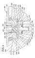
- FIG. 1is an isometric section view of a precursor material delivery system 100 of an ALD reactor 102 , which comprises an exemplary environment of use for valves 104 a – 104 e , in accordance with a first preferred embodiment.
- a supply of precursor materialis stored in a precursor container 106 , where it is heated and vaporized before flowing through a flow path 110 of the precursor material delivery system 100 (generally from left to right in FIG. 1 ) and into a reaction chamber 112 .
- ALD reactor 102will typically have two or more precursor material delivery systems 100 connected to reaction chamber 112 .
- Precursor material delivery system 100includes electric heaters 116 and 118 for heating precursor materials in the flow path 110 .
- Valves 104 a – 104 eare used to control the flow of precursor material and regulate pressure of the precursor vapor at different stages in precursor material delivery system 100 .
- Precursor material delivery system 100preferably includes removable modules 120 having bodies 122 machined from solid blocks of thermally conductive material, such as aluminum, titanium, or stainless steel.
- Modules 120have various different functions, such as storage, vaporization, valving, filtering, and pulsing of precursor materials, and purging with inert gases.
- Modules 120preferably all have a heavy construction that promotes diffusive conduction of heat from heaters 116 and 118 to promote a smooth temperature gradient along the length of precursor material delivery system 100 , increasing in temperature toward reaction chamber 112 .
- the downstream heater 118may operate at a temperature slightly higher than the upstream heater 116 to facilitate the temperature gradient. In an alternative embodiment (not shown), a greater number of heating zones may be employed.
- a positive temperature gradientis important for preventing undesirable condensation or freezing of precursor gases in flow path 110 at any point downstream from precursor container 106 .
- the magnitude of the temperature gradientis not typically important, so long as the temperature and pressure conditions within flow path 110 are sufficient to prevent condensation or freezing of precursor vapors.
- heaters 116 and 118may typically be operated at temperatures in the range of approximately 50° C. and 300° C.
- a volume module 124is provided downstream from the precursor container 106 for preparing a dose of gas-phase precursor material.
- a particle filter module 128prevents particles from being transported from precursor container 106 into volume module 124 .
- Valve 104 dis a diaphragm valve used to control the timing and duration of pulses of precursor vapor introduced into the reaction chamber 112 by precursor material delivery system 100 .
- a diffusion barrier module 140includes valve 104 e for controlling the direction of an inert gas flow in a barrier section 144 of flow path 110 located between diaphragm valve 104 d and reaction chamber 112 .
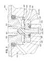
- FIG. 2is a cross-section elevation view of a diaphragm valve 200 in accordance with a preferred embodiment, which is exemplary of valves 104 a – 104 e ( FIG. 1 ).
- diaphragm valve 200includes a valve body 210 that defines a valve passage 214 through which a medium can flow when diaphragm valve 200 is open.
- Valve passage 214includes an inlet 216 and an outlet 218 , which are selectively interruptible by a flexible diaphragm 220 , which blocks valve passage 214 when flexed to a closed position, as shown in FIG. 2 .
- Valve body 210is preferably integrally formed with the body 122 of one of the modules 120 of precursor material delivery system 100 ( FIG. 1 ). Forming valve passage 214 in module body 122 facilitates connection of inlet 216 and outlet 218 to adjoining portions of flow path 110 in adjoining modules 120 of precursor material delivery system 100 . Alternatively, valve body 210 may comprise a separate structure, which, when used in an ALD precursor material delivery system 100 , may be coupled to the module body 122 . Valve body 210 is preferably formed from a solid billet of material having good thermal conductivity. However, valve body 210 may, alternatively, be formed of multiple parts or by means other than machining from a solid billet, such as by molding or casting, for example.
- Suitable valve body materials for use in ALD system 102include aluminum, titanium, and stainless steel. Other materials such as copper, brass, other metals, and molded materials such as high temperature plastics and molded metals may also be suitable for use in valve body 210 depending on the environment in which diaphragm valve 200 is to be used.
- valve passage 214may include a straight-through passage extending transversely to diaphragm valve 200 .
- Still further alternativesmay include a weir formed in the valve body between the inlet and outlet.
- Many other means and structuresmay be used for defining valve passage 214 to handle the flow of a medium such as a fluid (liquid and/or gas) or slurry.
- Inlet 216 and outlet 218extend into a cylindrical blind bore 226 bordered by a rim 228 against which diaphragm 220 is secured. Bore 226 is deep enough to accommodate a valve seat 230 against which diaphragm 220 is pressed when transitioned to the closed position. Bore 226 is also sized to allow the medium to flow through valve passage 214 between inlet 216 and outlet 218 when diaphragm 220 is transitioned to the open position ( FIG. 4 ). Thus, bore 226 forms side and bottom boundaries of a central chamber 232 ( FIG. 4 ) of valve passage 214 .
- diaphragm 220is a flexible disc-shaped member having a central section that is pressed against or pulled away from valve seat 230 selectively in response to an applied actuation force.
- Diaphragm 220includes a first side 234 positioned proximal to valve passage 214 and forming an upper boundary of central chamber 232 .
- a second side 236 of diaphragm 220 opposite first side 234is engaged by a means for applying actuation force, such as an actuator 240 .
- Diaphragm valve 200is shown oriented with actuator 240 extending vertically from diaphragm 220 and valve passage 214 .
- diaphragm valve 200could also be oriented with actuator 240 extending to the side of, below, or at an incline relative to diaphragm 220 and valve passage 214 .
- diaphragm 220 , valve passage 214 , and other parts of diaphragm valve 200may be oriented in many different ways.
- the valve passagemay be oriented at an angle to promote drainage across the weir when the valve is in the open position, as is common in prior art diaphragm valves.
- top, bottom, upper, lower, side, front, back, and other similar designationsare used as a matter of convenience to describe the preferred embodiment, oriented as it is shown in the drawing figures, and should not be construed as limiting the scope of the invention.
- Diaphragm 220is preferably formed of a flexible plastic or elastomeric material.
- diaphragm 220is preferably formed of a thin, molded disc of a plastic material such as polytetrafluoroethylene (“PTFE”), which may be of the type sold by E. I. du Pont de Nemours & Company, Wilmington, Del., USA, under the TEFLON® trademark.
- PTFEis a preferred diaphragm material for use in a precursor delivery system that delivers aluminum chloride (AlCl 3 ) to the reaction chamber 112 .
- diaphragm 220While PTFE is desirable for its purity, inertness, chemical resistance, heat resistance, and toughness, other plastic materials, such as polyvinylidene fluoride (“PVDF”), for example, may also be suitable for use in diaphragm 220 .
- PVDFpolyvinylidene fluoride
- diaphragm 220may preferably be formed of an elastomer material, such as VITON® brand fluoroelastomer (FKM) made by DuPont Dow Elastomers LLC, Wilmington, Del., USA.
- FKMVITON® brand fluoroelastomer
- elastomeric materials for diaphragm 220include ethylene propylene diene monomer (“EPDM”); silicone rubber; nitrile rubber; chloroprene rubber (neoprene); natural rubber; and perfluorinated elastomers (FFKM), such as KALREZ® made by DuPont Dow Elastomers LLC, CHEMRAZ® made by Greene, Tweede & Co., Medical & Biotechnology Group, Hatfield, Pa., USA, and SIMRIZ® sold by Freudenberg-NOK, Madison, Mich., USA.
- EPDMethylene propylene diene monomer
- silicone rubbernitrile rubber
- chloroprene rubberneoprene
- natural rubbersuch as KALREZ® made by DuPont Dow Elastomers LLC, CHEMRAZ® made by Greene, Tweede & Co., Medical & Biotechnology Group, Hatfield, Pa., USA, and SIMRIZ® sold by Freudenberg-NOK, Madison,
- elastomersare less desirable than plastics due to the inferior high-temperature resistance of elastomers and the tendency of fillers in some elastomers to contaminate precursor materials flowing through valve passage 214 .
- elastomerssuch as VITON, EPDM, and others have good chemical resistance, good purity, and excellent sealing capabilities, making them preferred diaphragm materials for use with many of the ALD precursors used in semiconductor processing.
- diaphragm 220may be formed of metal, especially when the temperature of the medium will exceed 260° C., having the potential to degrade elastomer materials.
- metal diaphragmsare more vulnerable to fatigue-related failure and breakage than plastic and elastomeric diaphragms.
- Diaphragm 220is preferably formed of a solid disc of material, but may also include structures that are not disc shaped, composite structures, and any other flexible shapes and structures that can be transitioned between open and closed positions.
- the term “diaphragm”is to be construed broadly to include any member that both borders valve passage 214 when open and can be moved or flexed to a closed position, thereby blocking valve passage 214 .
- the valve passage 214 , diaphragm 220 , and valve seat 230may be coated with a passivation layer.
- the passivation layermay comprise an oxide, such as Al 2 O 3 , ZrO 2 , HfO 2 , TiO 2 , Ta 2 O 5 , SnO 2 , or Nb 2 O 5 ; a nitride, such as AlN, ZrN, HfN, TiN, TaN, NbN, or BN; a carbide, such as TiC, TaC, ZrC, or HfC; or mixtures thereof.
- other passivation materials and coatingsmay be used.
- Passivationis particularly important when using halide-based precursors, to prevent exchange reactions between the halide-based precursors and the metal typically used in valve body 210 and valve seat 230 .
- the specific composition of the passivation layeris selected for compatibility with the type of precursor or other medium with which diaphragm valve 200 is used. Other considerations, such as thermal properties, electrical properties, durability, and malleability, for example, may also be important factors in the selection of the material used for passivation.
- Actuator 240is operably coupled to diaphragm 220 for applying an actuation force for transitioning diaphragm 220 from the open position to the closed position.
- actuator 240transitions diaphragm 220 from the closed position to the open position, or in both directions.
- the preferred diaphragm valve 200 for use in precursor material delivery system 100is of a normally closed configuration.
- Actuator 240preferably includes a solenoid 246 that can be energized by application of an electric current to drive a plunger 250 that transmits force to diaphragm 220 . Solenoid 246 is the preferred actuator for diaphragm valve 200 due to its speed and generally low maintenance requirements.
- actuator 240may include a different means for actuating diaphragm 220 , such as a pneumatic or hydraulic cylinder, for example.
- Other devices and methods of actuating diaphragm 220such as piezoelectric devices, for example, may also be used.
- Plunger 250 of actuator 240includes a first end section 256 engaged by solenoid 246 and a second end section 258 coupled to diaphragm 220 .
- Plunger 250may be coupled to diaphragm 220 in many ways.
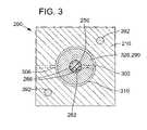
- diaphragm 220may include a head 262 or ball end that extends from second side 236 of diaphragm 220 and snaps into lateral openings 266 ( FIG. 3 ) in second end section 258 of plunger 250 .
- This snap-fit connection between head 262 and plunger 250allows actuator 240 to pull the central section of diaphragm 220 away from valve seat 230 . It may also allow diaphragm 220 to be conveniently removed for repair or replacement without completely disassembling actuator 240 , plunger 250 , and other components of diaphragm valve 200 .
- Actuator 240includes a stop 276 secured to solenoid 246 at its distal end 278 and extending into the center of solenoid 246 to limit outward travel of plunger 250 .
- Stop 276is preferably formed of a magnetic material (i.e., a material having a high permeance) to reduce the reluctance in the magnetic circuit of solenoid 246 . More specifically, stop 276 reduces the high-reluctance air gap between distal end 278 of solenoid 246 and plunger 250 , thereby reducing the overall reluctance in the magnetic circuit and intensifying the magnetomotive force exerted on plunger 250 by solenoid 246 , when energized.
- the magnetomotive actuation forceis further increased as plunger 250 moves closer to stop 276 , i.e., when the low permeance gap between plunger 250 and stop 275 is reduced.
- stop 276is made of a nonmagnetic material or omitted entirely.
- a spring 280preferably interposed between stop 276 and plunger 250 , biases plunger 250 and diaphragm 220 toward the closed position wherein first side 234 of diaphragm 220 is pressed against valve seat 230 to block valve passage 214 .
- Spring 280is preferably seated in a counterbore in first end section 256 of plunger 250 , but alternative embodiments may involve placement of spring 280 in another location or use of other means for biasing plunger 250 relative to valve seat 230 .
- plunger 250is biased away from valve seat 230 , and plunger 250 is driven toward valve seat 230 when actuator 240 is activated.
- spring 280may be omitted, in which case diaphragm 220 may be driven in both the opening and closing directions by actuator 240 .
- spring 280is omitted and diaphragm 220 has a domed shape that is inherently resilient, providing an integral return spring force. Skilled persons will appreciate that many other means and devices may be employed for effecting return of diaphragm 220 to its normal position.
- diaphragm 220is secured to valve body 210 by a heating body 290 to form a substantially hermetic seal along a perimeter of diaphragm 220 where it is clamped against rim 228 by heating body 290 .
- Heating body 290includes a proximal end 294 that is relieved to define a space 296 adjacent second side 236 of diaphragm 220 .
- Space 296provides clearance for diaphragm 220 when diaphragm 220 is moved to the open position ( FIG. 4 ) and is substantially enclosed, although a small amount of clearance is provided around plunger 250 to allow plunger 250 to move freely in response to activation of actuator 240 .
- the clearance around plunger 250 , the space 296 , and any other passages in fluid communication with space 296are preferably sealed to prevent leakage beyond valve 200 in the event that precursor or other medium escapes around the perimeter of diaphragm 220 or in the event that diaphragm 220 ruptures.
- it may not be necessary to hermetically seal space 296particularly when diaphragm valve 200 is used in applications other than ALD systems.
- enclosed space 296is defined, at least in part, by proximal end 294 of heating body 290 .
- space 296is defined by one or more other components of diaphragm valve 200 , such as, for example, the valve body, the actuator housing, a valve stem, or another structural member extending proximal to second side 236 of diaphragm 220 .
- venting of enclosed space 296may provide one or more benefits. For example, venting can reduce or prevent resistance to the movement of diaphragm 220 that would otherwise be caused by compression or expansion of gases trapped in space 296 .
- suctionmay be applied in conjunction with venting to reduce a pressure differential acting on diaphragm 220 . Suction can also be applied to generate a vacuum of the same pressure as the medium in valve passage 214 , thereby equalizing the pressures on respective first and second sides 234 and 236 of diaphragm 220 .
- suctioncan be applied to venting to achieve a pressure in space 296 that is slightly less than the medium in valve passage 214 , to thereby assist actuator 240 in opening diaphragm 220 .
- the ventingmay advantageously reduce the force necessary to actuate diaphragm 220 and move it to the open position, and may also reduce the spring force necessary to return diaphragm 220 to the closed position. Similar force reductions are possible in an alternative normally open configuration, in which case the direction of actuation and spring forces would be reversed. By reducing forces needed to transition diaphragm 220 between the open and closed positions, venting may also extend the life of diaphragm 220 and prevent solenoid burnout.
- Extending the life of valves 104 a - e in ALD precursor material delivery system 100can significantly decrease downtime and improve yields in ALD reactor 102 .
- Applying suction to space 296has the further benefit of improving safety, in that any gas that leaks around or through diaphragm 220 is pumped away. This feature is of particular benefit when using toxic precursor materials, which might otherwise leak into human workspaces.
- Applying a vacuum to space 296also reduces the density of gas in valve space 296 , which restricts a convective pathway from diaphragm 220 to actuator 240 .
- Ventingis preferably accomplished by a venting passage, an embodiment of which is described below with reference to FIGS. 2 and 3 .
- FIG. 3is a cross section view of diaphragm valve 200 taken along lines 3 — 3 of FIG. 2 .
- the venting passageincludes a first vent passage section 302 extending through heating body 290 and communicating with space 296 ; a second vent passage section 306 passing through valve body 210 ; and an annular connecting passage 310 that extends around a mid-section of heating body 290 to link together the first and second vent passage sections 302 and 306 .
- the venting passagefollows a different path, through one or more other parts of diaphragm valve 200 .
- connection of pump 316 to the venting passagemay include connecting the pump 316 to a manifold (not shown) that serves one or more of the diaphragm valves 104 a – 104 e and, possibly, other modules 120 of precursor material delivery system 100 where suction is needed.
- Pump 316is operable to draw a vacuum in space 296 relative to the pressure outside of valve body 210 (typically atmospheric pressure).
- Resilient seals 328 and 382are provided to prevent leakage around heating body 290 and to allow a vacuum to be achieved in space 296 behind diaphragm 220 .
- vacuumis used loosely to describe a fluid pressure that is lowered from its atmospheric or otherwise normal pressure.
- the suction generated by pump 316preferably reduces the pressure in space 296 to a pressure that is the same as or close to the fluid pressure of the medium flowing through valve passage 214 , thereby equalizing or nearly equalizing a differential force on diaphragm 220 .
- the pressure in space 296is increased by application of a positive fluid pressure instead of suction.
- pump 316may be omitted in some embodiments.
- pump 316 or another means for generating suctionis operable to reduce the pressure in space 296 to between approximately 0.1 mbar and approximately 20 mbar, which is comparable to the operating pressure of precursor vapors in flow path 110 and valve passage 214 .
- Diaphragm valve 200preferably includes features that enhance reliability when valve 200 is used to control the flow of a high temperature medium, such as an ALD precursor vapor used for depositing a thin film on a semiconductor wafer substrate, for example.
- a high temperature mediumsuch as an ALD precursor vapor used for depositing a thin film on a semiconductor wafer substrate
- the improved thermal design of diaphragm valve 200may provide advantages over conventional diaphragm valves, in which solenoid actuators (or other types of actuators) are vulnerable to heat-related failure.
- one conventional solenoid-actuated diaphragm valveis rated for operating temperatures of up to 140° C.
- the solenoidWhen the operating temperature exceeds 140° C., the solenoid can overheat and melt a plastic bobbin supporting the solenoid coil and/or melt insulation around the coil windings, thereby causing blockage of the plunger, short circuiting of the coil, and other modes of failure.
- high operating temperaturescan cause failure due to permanent deformation of structural components, melting or deformation of resilient seal materials in the actuator, and other causes.
- Heat conducted to actuator 240can also cool diaphragm 220 or valve body 210 enough to cause the medium to condense or freeze within valve passage 214 or on surfaces bordering valve passage 214 .
- Condensation of the mediumis particularly troublesome in an ALD precursor material delivery system 100 , because particles or condensation can cause blockage in the delivery system 100 or may propagate into the reaction chamber 112 , causing flaws in the films being formed.
- Condensation on the surfaces of diaphragm 220 and/or valve seat 230can also cause leakage of precursor past valve 200 , when closed, which can cause non-ALD growth in reaction chamber 112 .
- the operating temperaturewill depend on the vapor pressure of the particular precursor medium, but will typically be in the range of 130° C. to 220° C.
- the precursoris gradually heated with a positive temperature gradient toward reaction chamber 112 .
- the heatis provided by heaters 116 and 118 in two zones along precursor material delivery system 100 , although a different number of zones and heaters may be used in an alternative embodiment (not shown). Heat may be provided by means other than electric heaters, but will generally result in the conduction of heat into valve body 210 .
- valve body 210 and bodies 122 of other modules 120are preferably formed of a thermally conductive material such as aluminum, titanium, or stainless steel.
- Heating body 290is positioned in thermal contact with valve body 210 and extends proximal to second side 236 of diaphragm 220 to thereby form a thermally conductive pathway between valve body 210 and diaphragm 220 .
- the thermally conductive pathwayfacilitates maintenance of an operating temperature at diaphragm 220 sufficient to prevent condensation in valve passage 214 .
- Heating body 290is interposed between diaphragm 220 and actuator 240 and includes a central opening 322 in alignment with diaphragm 220 and actuator 240 , and through which plunger 250 extends for coupling actuator 240 to diaphragm 220 .
- Second end section 258 of plunger 250is preferably formed of a thermally conductive material and sized to closely but slidably fit within central opening 322 , so that heat is readily transmitted from heating body 290 to diaphragm 220 through plunger 250 .
- a core 326 of heating body 290extends into a counterbore in valve body 210 above rim 228 and is shaped to define the annular connecting passage 310 ( FIG. 3 ).
- a seal 328such as an O-ring, is positioned around core 326 to form a hermetic seal between heating body 290 and valve body 210 at an axially distal location relative to annular connecting passage 310 .
- a flange 332 of heating body 290extends radially outward from core 326 adjacent an outer surface 334 of valve body 210 .
- Flange 332contacts outer surface 334 along a relatively large area, thereby improving heat conduction from valve body 210 to heating body 290 .
- Flange 332also provides a structure suitable for securing heating body 290 to valve body 210 , for example, with one or more screws or other fasteners 392 ( FIGS. 2–3 ).
- Flange 332also compresses seal 328 against valve body 210 when secured by fasteners 392 .
- Heating body 290is preferably comprised of a material having a high thermal conductivity, such as aluminum, stainless steel, titanium, copper, or other metals, for example.
- valve seat 230When diaphragm 220 is in the closed position in contact with valve seat 230 , heat is conducted to diaphragm 220 via valve seat 230 . Conduction from valve seat 230 helps replace in diaphragm 220 the heat lost by dissipation through plunger 250 and actuator 240 into the surrounding environment.
- Valve seat 230is, accordingly, formed of a material having a relatively high thermal conductivity, such as aluminum, titanium, or another metal, for example.
- valve seat 230When used with a diaphragm made of an elastomeric material, valve seat 230 preferably includes a substantially flat annular seating surface 342 extending radially from inlet 216 .
- Seating surface 342provides increased contact area between diaphragm 220 and valve seat 230 when diaphragm 220 is closed.
- the increased contact areareduces the contact resistance (thermal) between valve seat 230 and diaphragm 220 .
- valve seat 230contacts a substantial portion of first side 234 of diaphragm 220 to promote heat transfer from valve seat 230 to diaphragm 220 along a thermally effective contact area opposite where plunger 250 contacts second side 236 of diaphragm.
- the area of contact between seating surface 342 and diaphragm 220is comparable to the contact area between plunger 250 and diaphragm 220 .
- valve seat 230When diaphragm 220 is closed, valve seat 230 may contact between approximately 5% and 100% of the portion of first side 234 of diaphragm 220 exposed to central chamber 232 . More preferably, valve seat 230 may contact between approximately 12% and 50% of the exposed area of first side 234 of diaphragm 220 , when diaphragm 220 is closed.
- Seating surface 342may also be polished or otherwise made smooth to further reduce contact resistance and to reduce leakage of medium between valve seat 230 and diaphragm 220 when diaphragm 220 is in the closed position.
- a passivation layer over first side 234 of diaphragm 220can further enhance conduction of heat from valve seat 230 to diaphragm 220 .
- a passivation layer on first side 234may comprise a layer of aluminum oxide (Al 2 O 3 ) or another metallic coating having a thickness of between approximately 10 nm and approximately 100 nm.
- FIG. 5is a cross sectional view of an alternative embodiment diaphragm valve 500 including a plastic diaphragm 520 .
- plastic diaphragm 520is preferably formed of PTFE or another resilient, high-purity, chemically inert material, such as PVDF, for example. Because plastic diaphragm 520 does not seal as easily as elastomeric diaphragms, diaphragm valve 500 includes a modified valve seat 530 having a ring-shaped seating ridge 522 that extends upwardly from seating surface 542 toward diaphragm 520 .
- Seating ridge 522is sufficiently prominent and sized to permanently deform first side 534 of diaphragm 520 when diaphragm 520 is pressed against valve seat 530 .
- Seating ridge 522surrounds inlet 516 and is preferably located immediately adjacent inlet 516 to reduce the amount of spring force necessary to cause permanent deformation of diaphragm 520 .
- seating ridge 522may be located outwardly of inlet 516 or in another location.
- Seating ridge 522may be flat-topped, as shown in FIG. 5 , or may have another shape, such as a knife edge.
- seating ridge 522differs from knife-edge valve seats of the prior art in that seating ridge 522 is short enough to allow the first side 534 of diaphragm 520 to be pressed against the surrounding seating surface 542 after seating ridge 522 has formed a ring-shaped hit channel 544 in first side 534 .
- prior art diaphragm valvesprevent leaks by using sharp valve seats that are tall enough to prevent areal contact between the diaphragm and flat surfaces around the sharp seating edge.
- sealing interferenceis best prevented by improved heat transfer between the valve seat 530 and diaphragm 520 , to prevent particle formation due to cooling of the diaphragm.
- Seating ridge 522is preferably between approximately 0.5 mm and 1.5 mm in height above seating surface 542 to provide the desired permanent deformation of hit channel 544 , while allowing areal contact between first side 534 of diaphragm 520 and seating surface 542 of valve seat 530 after hit channel 544 has been formed.
- the initial formation of hit channel 544 in first side 534 of diaphragm 520may require a break-in period in which valve 500 is cycled prior to use.
- annular seating surface 542may be sized and shaped similarly to that of the seating surface 342 of the embodiment of FIGS. 2–4 , described above.
- the area of contact between seating surface 542 and diaphragm 520may be comparable to the contact area between a second end section 558 of plunger 550 and a second side 536 of diaphragm 520 .
- valve seat 530may contact between approximately 5% and 100% of the portion of first side 534 of diaphragm 520 exposed to central chamber 532 and, more preferably, between approximately 12% and 50% of the exposed area.
- Valve seat 530may include a polished surface finish and/or passivation similar to the surface treatments described above in connection with valve seat 230 ( FIGS. 2–4 ) of the type used with elastomeric diaphragm 220 . Because the plastic material used in diaphragm 520 of FIG. 5 is stiffer than elastomeric materials of the diaphragm 220 of FIGS. 2–4 , flexibility may be improved in diaphragm 520 by reducing the thickness of diaphragm 520 or, preferably, by forming an annular thin region 552 between a head 562 of diaphragm 520 and where diaphragm is mounted against a rim 528 of valve body 510 .
- Diaphragm 520 and valve seat 530are preferably rotationally secured to prevent relative rotation that can cause leakage due to misalignment between seating ridge 522 and hit channel 544 . Preventing relative rotation between diaphragm 520 and valve seat 530 also facilitates the formation on first side 534 of a micro-roughness that mates against corresponding micro-roughness of seating surface 542 , to thereby promote a hermetic seal.
- a thermally resistive memberis preferably interposed between valve passage 214 and actuator 240 to restrict or throttle the transfer of heat from valve passage 214 (i.e., from heating body 210 and/or diaphragm 220 ) to actuator 240 .
- the thermally resistive membermay comprise one or more structures for attenuating heat transfer between valve passage 214 and actuator 240 , or between valve body 210 and actuator 240 , or between heating body 290 and actuator 240 , or between actuator 240 and one or more other parts of diaphragm valve 200 .
- thermally resistive membercomprises a section of reduced cross sectional area between valve passage 214 and/or valve body 210 and actuator 240 .
- plunger 250may include a hollow region 348 between respective first and second end sections 256 and 258 . Hollow region 348 and the surrounding thin cylindrical wall of plunger 250 attenuate heat transfer between diaphragm 220 and actuator 240 . As described above, attenuation of heat transfer prevents heat-related failure of solenoid 246 and cooling of diaphragm 220 , which can otherwise result in condensation of the medium in valve passage 214 .
- plunger 250may have a composite construction, wherein first end section 256 is formed of a magnetic material, second end section 258 is formed of a thermally conductive material (for conducting heat from heating body 290 to diaphragm 220 ), and an insulating central section 352 between respective first and second end sections 256 and 258 .
- Central section 352may be formed of a material having a substantially lower thermal conductivity than second end section 258 or may have a structure resulting in lower thermal conductivity than second end section 258 .
- valve stem 360supporting actuator 240 over and apart from heating body 290 and valve body 210 .
- Valve stem 360may include a section of reduced cross sectional area 364 for attenuating heat transfer between heating body 290 and actuator 240 .
- valve stem 360preferably contacts heating body 290 and/or valve body 210 along only a very small area, if at all.
- valve stem 360may be supported on a small step 368 of a central boss 372 of heating body 290 .
- An insulating pedestal 376 formed of a thermally resistive material such as plastic or ceramicmay extend around or be positioned around a perimeter of flange 332 of heating body 290 to separate valve stem 360 from heating body 290 .
- Insulating pedestal 376may comprise a ring of insulating material, or may, alternatively, comprise a set of posts extending from flange 332 about its perimeter.
- An elastomeric or plastic seal 382is positioned around boss 372 and between heating body 290 and valve stem 360 . Seal 382 prevents leakage of gases between heating body 290 and valve stem 360 .
- An annular dead air space 386may be formed between valve stem 360 and heating body 290 and between seal 382 and insulating pedestal 376 . Dead air space 386 further insulates valve stem 360 from heating body 290 .
- Actuator 240may be secured to valve stem 360 by press fitting of solenoid 246 onto valve stem 360 , by adhesives, or by other means. Valve stem 360 and heating body 290 are attached to valve body 210 by one or more screws 392 extending through holes in the radial portion of valve stem 360 and the flange 332 of heating body 290 .
- Screws 392are threaded into valve body 210 and thermally insulated from valve stem 360 by insulating washers 396 positioned under the heads of screws 392 .
- Insulating washers 396may be made of a plastic material such as PTFE, for example.
- a thermally insulating slide bushing 402is interposed between plunger 250 and actuator 240 .
- Slide bushing 402is preferably formed of a thermally insulating plastic material such as PTFE that also has a low coefficient of sliding friction against the inner surface of valve stem 360 within which first end section 256 of plunger 250 rides.
- Slide bushing 402advantageously may inhibit heat transfer between plunger 250 and actuator 240 , reduce frictional resistance to movement of plunger 250 , and reduce wear and particle generation that can foul the movement of plunger 250 within actuator 240 .
- a blocking member 410is interposed between plunger 250 and stop 276 .
- Blocking member 410is preferably comprised of a durable plastic material that cushions the impact of plunger 250 against stop 276 when solenoid 246 is energized. Cushioning of the impact can prevent cracking of stop 276 and/or plunger 250 , thereby preventing the formation of particles that can foul the movement of plunger 250 within actuator 240 .
- a suitable plastic material for blocking member 410is PTFE.
- Blocking member 410may also have thermal insulating properties to attenuate heat transfer between plunger 250 and stop 276 when plunger 250 is in the fully open position, in contact with blocking member 410 .
- blocking member 410When formed of a nonmagnetic material, such as PTFE or another plastic, blocking member 410 introduces a magnetic discontinuity between stop 276 and plunger 250 that can reduce a “release time” after removal of electric current from solenoid 246 before spring 280 will begin to move plunger 250 away from stop 276 .
- the magnetic discontinuity introduced by blocking member 410reduces the magnetic field at the extreme distal end of first end section 256 of plunger 250 by providing a nonmagnetic separation between the magnetically conductive stop 276 and the magnetically conductive first end section 256 of plunger 250 .
- the attractive magnetic force on plunger 250 that is generated by solenoid 246is not immediately removed when electric current to solenoid 246 is cut off.
- Blocking member 410reduces release time by reducing the holding force between solenoid 246 and plunger 250 . Reducing the release time results in quicker switching from the on state to the off state, making it possible to shorten the total open time of diaphragm valve 200 .
- Prior art diaphragm valvessuch as the ones described in U.S. Pat. No. 5,326,078 of Kimura and U.S. Pat. No. 6,116,267 of Suzuki et al., for example, include a valve seat having a sharp seating surface for deforming the diaphragm or increasing localized pressure on the diaphragm when it is pressed against the valve seat.
- diaphragm 220may be comprised of an elastomeric material such as VITON® or EPDM, for example. When exposed to certain heated precursors and chemicals, such as ZrCl 2 , for example, elastomer materials can become brittle, making them vulnerable to cracking and shearing against a sharp valve seat.
- seating surface 342 of valve seat 230is characterized by an absence of sharp features, which may help prevent scoring and eventual shearing or cracking of diaphragm 220 .
- Seating surface 342is preferably larger than 5 mm 2 and more preferably larger than 25 mm 2 . While it is desirable to size valve seat 230 large enough to prevent diaphragm 220 from shearing, the shape and size of valve seat 230 may, nevertheless, be selected so that the biasing force from spring 280 will cause slight surface deformation of first side 234 of diaphragm 220 .
- Surface deformationcauses first side 234 to better conform to seating surface 342 , thereby reducing leakage of medium that can otherwise result from micro-roughness of first side 234 and/or seating surface 342 .
- Surface deformationmay include elastic deformation, or plastic deformation, or both.
- a smooth or polished surface finish of seating surface 342may further improve the ability of diaphragm 220 to provide a leak-tight seal when pressed against seating surface 342 .
- valve seat 530 for use with a plastic diaphragm 520preferably includes a seating ridge 522 extending from the seating surface 542 around inlet 516 .
- the seating ridge 522causes plastic deformation of first side 534 of diaphragm 520 when it is pressed against valve seat 530 during a break-in period.
- Diaphragm 520can be pre-cycled to help break it in before commencing use of diaphragm valve 500 .
- Plastic deformation occurring during pre-cycling or a break-in periodimparts a ring-shaped hit channel 544 to diaphragm 520 that tightly mates against seating ridge 522 to prevent leakage.
- a similar sharp edge valve seatmay also be desirable to increase localized sealing pressure when diaphragm 520 is made of metal, although it may be unnecessary or undesirable to plastically deform a metal diaphragm.
- valve seat 230 , 530 and diaphragm 220 , 520are secured to the respective valve body 210 , 510 and plunger 250 , 550 to thereby prevent relative rotation. Preventing relative rotation between the valve seat and diaphragm ensures that the same location on diaphragm 220 , 520 contacts valve seat 230 , 530 in the same place every time the diaphragm valve 200 , 500 is closed.
- FIG. 4is an enlarged cross section view detailing valve passage 214 , valve seat 230 , and diaphragm 220 , with the diaphragm 220 shown transitioned to the open position.
- annular seating surface 342 of valve seat 230is sufficiently large so that first side 234 of diaphragm 220 , when flexed to its slightly convex closed position, will not contact an outer peripheral edge 418 of seating surface 342 .
- Seating surface 342may also be curved along outer peripheral edge 418 , as shown in FIG. 4 , or may be slightly crowned (not shown), to further prevent scoring or shearing of diaphragm 220 .
- Valve seat 230is generally pedestal-shaped and includes a threaded neck 422 extending opposite seating surface 342 . Valve seat 230 is screwed into valve body 210 to achieve good thermal contact. Preferably, valve seat 230 is threaded into an inlet portion of valve passage 214 . However, in an alternative embodiment (not shown), inlet 216 and outlet 218 are reversed so that valve seat 230 is threaded into an outlet passage formed in valve body 210 . Valve seat 230 may be coated with a passivation layer in a manner similar to diaphragm 220 and valve passage 214 (as described above) to prevent corrosion of valve seat 230 or buildup of precursor materials on seating surface 342 or inside inlet 216 .
- a seat O-ring 430is interposed between an upper pedestal portion of valve seat 230 and a lower surface of blind bore 226 of valve body 210 to provide a leak-tight seal between valve seat 230 and valve body 210 .
- a spacer ring 440 or shimis interposed between upper pedestal portion of valve seat 230 and a floor of blind bore 226 of valve body 210 for establishing an axial position of valve seat 230 relative to valve body 210 .
- Spacer ring 440prevents overcompression of O-ring 430 and establishes an axial position of seating surface 342 relative to valve body 210 and diaphragm 220 .
- Precise axial positioning of seating surface 342allows for improved control of the seating pressure of diaphragm 220 against seating surface 342 , thereby enhancing leak-tightness without applying excessive force that might cause scoring on first side 234 of diaphragm 220 .
Landscapes
- Engineering & Computer Science (AREA)
- General Engineering & Computer Science (AREA)
- Mechanical Engineering (AREA)
- Details Of Valves (AREA)
Abstract
Description
Claims (66)
Priority Applications (8)
| Application Number | Priority Date | Filing Date | Title |
|---|---|---|---|
| US10/609,339US7021330B2 (en) | 2003-06-26 | 2003-06-26 | Diaphragm valve with reliability enhancements for atomic layer deposition |
| PCT/US2004/020916WO2005003605A2 (en) | 2003-06-26 | 2004-06-28 | Diaphragm valve for atomic layer deposition |
| DE112004001147TDE112004001147T5 (en) | 2003-06-26 | 2004-06-28 | Diaphragm valve for the deposition of atomic layers |
| JP2006517779AJP2007528962A (en) | 2003-06-26 | 2004-06-28 | Diaphragm valve for atomic layer deposition |
| GB0612855AGB2426808C (en) | 2003-06-26 | 2004-06-28 | Diaphragm valve for atomic layer deposition |
| GB0525685AGB2418005B (en) | 2003-06-26 | 2004-06-28 | Diaphragm valve for atomic layer deposition |
| KR1020057024768AKR20060084360A (en) | 2003-06-26 | 2004-06-28 | Diaphragm Valves for Atomic Layer Deposition |
| US11/278,482US7191793B2 (en) | 2003-06-26 | 2006-04-03 | Diaphragm valve for atomic layer deposition |
Applications Claiming Priority (1)
| Application Number | Priority Date | Filing Date | Title |
|---|---|---|---|
| US10/609,339US7021330B2 (en) | 2003-06-26 | 2003-06-26 | Diaphragm valve with reliability enhancements for atomic layer deposition |
Related Child Applications (1)
| Application Number | Title | Priority Date | Filing Date |
|---|---|---|---|
| US11/278,482ContinuationUS7191793B2 (en) | 2003-06-26 | 2006-04-03 | Diaphragm valve for atomic layer deposition |
Publications (2)
| Publication Number | Publication Date |
|---|---|
| US20040262562A1 US20040262562A1 (en) | 2004-12-30 |
| US7021330B2true US7021330B2 (en) | 2006-04-04 |
Family
ID=33540851
Family Applications (2)
| Application Number | Title | Priority Date | Filing Date |
|---|---|---|---|
| US10/609,339Expired - Fee RelatedUS7021330B2 (en) | 2003-06-26 | 2003-06-26 | Diaphragm valve with reliability enhancements for atomic layer deposition |
| US11/278,482Expired - LifetimeUS7191793B2 (en) | 2003-06-26 | 2006-04-03 | Diaphragm valve for atomic layer deposition |
Family Applications After (1)
| Application Number | Title | Priority Date | Filing Date |
|---|---|---|---|
| US11/278,482Expired - LifetimeUS7191793B2 (en) | 2003-06-26 | 2006-04-03 | Diaphragm valve for atomic layer deposition |
Country Status (1)
| Country | Link |
|---|---|
| US (2) | US7021330B2 (en) |
Cited By (304)
| Publication number | Priority date | Publication date | Assignee | Title |
|---|---|---|---|---|
| US7191793B2 (en) | 2003-06-26 | 2007-03-20 | Planar Systems, Inc. | Diaphragm valve for atomic layer deposition |
| US20080105901A1 (en)* | 2006-11-07 | 2008-05-08 | Kamal Tabatabaie | Atomic layer deposition in the formation of gate structures for iii-v semiconductor |
| US8122903B2 (en) | 2007-07-26 | 2012-02-28 | Parker-Hannifin Corporation | Close-coupled purgeable vaporizer valve |
| US20130104998A1 (en)* | 2010-07-08 | 2013-05-02 | Magna Steyr Fahrzeugtechnik Ag & Co. Kg | Electromagnetic valve for a pressure container |
| US20160357197A1 (en)* | 2013-12-09 | 2016-12-08 | Idive, Inc. | Adaptive Pressure Balancer |
| US9587759B2 (en) | 2013-09-20 | 2017-03-07 | Itt Manufacturing Enterprises Llc | Quick release valve compressor |
| US20200018421A1 (en)* | 2018-07-16 | 2020-01-16 | Asm Ip Holding B.V. | Diaphragm valves, valve components, and methods for forming valve components |
| US10720331B2 (en) | 2016-11-01 | 2020-07-21 | ASM IP Holdings, B.V. | Methods for forming a transition metal nitride film on a substrate by atomic layer deposition and related semiconductor device structures |
| US10784102B2 (en) | 2016-12-22 | 2020-09-22 | Asm Ip Holding B.V. | Method of forming a structure on a substrate |
| US10787741B2 (en) | 2014-08-21 | 2020-09-29 | Asm Ip Holding B.V. | Method and system for in situ formation of gas-phase compounds |
| US10797133B2 (en) | 2018-06-21 | 2020-10-06 | Asm Ip Holding B.V. | Method for depositing a phosphorus doped silicon arsenide film and related semiconductor device structures |
| US10804098B2 (en) | 2009-08-14 | 2020-10-13 | Asm Ip Holding B.V. | Systems and methods for thin-film deposition of metal oxides using excited nitrogen-oxygen species |
| US10818758B2 (en) | 2018-11-16 | 2020-10-27 | Asm Ip Holding B.V. | Methods for forming a metal silicate film on a substrate in a reaction chamber and related semiconductor device structures |
| US10832903B2 (en) | 2011-10-28 | 2020-11-10 | Asm Ip Holding B.V. | Process feed management for semiconductor substrate processing |
| US10829852B2 (en) | 2018-08-16 | 2020-11-10 | Asm Ip Holding B.V. | Gas distribution device for a wafer processing apparatus |
| US10844486B2 (en) | 2009-04-06 | 2020-11-24 | Asm Ip Holding B.V. | Semiconductor processing reactor and components thereof |
| US10847371B2 (en) | 2018-03-27 | 2020-11-24 | Asm Ip Holding B.V. | Method of forming an electrode on a substrate and a semiconductor device structure including an electrode |
| US10847366B2 (en) | 2018-11-16 | 2020-11-24 | Asm Ip Holding B.V. | Methods for depositing a transition metal chalcogenide film on a substrate by a cyclical deposition process |
| US10844484B2 (en) | 2017-09-22 | 2020-11-24 | Asm Ip Holding B.V. | Apparatus for dispensing a vapor phase reactant to a reaction chamber and related methods |
| US10851456B2 (en) | 2016-04-21 | 2020-12-01 | Asm Ip Holding B.V. | Deposition of metal borides |
| US10858737B2 (en) | 2014-07-28 | 2020-12-08 | Asm Ip Holding B.V. | Showerhead assembly and components thereof |
| US10867788B2 (en) | 2016-12-28 | 2020-12-15 | Asm Ip Holding B.V. | Method of forming a structure on a substrate |
| US10865475B2 (en) | 2016-04-21 | 2020-12-15 | Asm Ip Holding B.V. | Deposition of metal borides and silicides |
| US10867786B2 (en) | 2018-03-30 | 2020-12-15 | Asm Ip Holding B.V. | Substrate processing method |
| US10872771B2 (en) | 2018-01-16 | 2020-12-22 | Asm Ip Holding B. V. | Method for depositing a material film on a substrate within a reaction chamber by a cyclical deposition process and related device structures |
| US10883175B2 (en) | 2018-08-09 | 2021-01-05 | Asm Ip Holding B.V. | Vertical furnace for processing substrates and a liner for use therein |
| US10886123B2 (en) | 2017-06-02 | 2021-01-05 | Asm Ip Holding B.V. | Methods for forming low temperature semiconductor layers and related semiconductor device structures |
| US10892156B2 (en) | 2017-05-08 | 2021-01-12 | Asm Ip Holding B.V. | Methods for forming a silicon nitride film on a substrate and related semiconductor device structures |
| US10896820B2 (en) | 2018-02-14 | 2021-01-19 | Asm Ip Holding B.V. | Method for depositing a ruthenium-containing film on a substrate by a cyclical deposition process |
| US10910262B2 (en) | 2017-11-16 | 2021-02-02 | Asm Ip Holding B.V. | Method of selectively depositing a capping layer structure on a semiconductor device structure |
| US10914004B2 (en) | 2018-06-29 | 2021-02-09 | Asm Ip Holding B.V. | Thin-film deposition method and manufacturing method of semiconductor device |
| US10923344B2 (en) | 2017-10-30 | 2021-02-16 | Asm Ip Holding B.V. | Methods for forming a semiconductor structure and related semiconductor structures |
| US10928731B2 (en) | 2017-09-21 | 2021-02-23 | Asm Ip Holding B.V. | Method of sequential infiltration synthesis treatment of infiltrateable material and structures and devices formed using same |
| US10934619B2 (en) | 2016-11-15 | 2021-03-02 | Asm Ip Holding B.V. | Gas supply unit and substrate processing apparatus including the gas supply unit |
| US10943771B2 (en) | 2016-10-26 | 2021-03-09 | Asm Ip Holding B.V. | Methods for thermally calibrating reaction chambers |
| US10941490B2 (en) | 2014-10-07 | 2021-03-09 | Asm Ip Holding B.V. | Multiple temperature range susceptor, assembly, reactor and system including the susceptor, and methods of using the same |
| US10950432B2 (en) | 2017-04-25 | 2021-03-16 | Asm Ip Holding B.V. | Method of depositing thin film and method of manufacturing semiconductor device |
| USD913980S1 (en) | 2018-02-01 | 2021-03-23 | Asm Ip Holding B.V. | Gas supply plate for semiconductor manufacturing apparatus |
| US10975470B2 (en) | 2018-02-23 | 2021-04-13 | Asm Ip Holding B.V. | Apparatus for detecting or monitoring for a chemical precursor in a high temperature environment |
| US11001925B2 (en) | 2016-12-19 | 2021-05-11 | Asm Ip Holding B.V. | Substrate processing apparatus |
| US11004977B2 (en) | 2017-07-19 | 2021-05-11 | Asm Ip Holding B.V. | Method for depositing a group IV semiconductor and related semiconductor device structures |
| US11018002B2 (en) | 2017-07-19 | 2021-05-25 | Asm Ip Holding B.V. | Method for selectively depositing a Group IV semiconductor and related semiconductor device structures |
| US11015245B2 (en) | 2014-03-19 | 2021-05-25 | Asm Ip Holding B.V. | Gas-phase reactor and system having exhaust plenum and components thereof |
| US11018047B2 (en) | 2018-01-25 | 2021-05-25 | Asm Ip Holding B.V. | Hybrid lift pin |
| US11022879B2 (en) | 2017-11-24 | 2021-06-01 | Asm Ip Holding B.V. | Method of forming an enhanced unexposed photoresist layer |
| US11024523B2 (en) | 2018-09-11 | 2021-06-01 | Asm Ip Holding B.V. | Substrate processing apparatus and method |
| US11031242B2 (en) | 2018-11-07 | 2021-06-08 | Asm Ip Holding B.V. | Methods for depositing a boron doped silicon germanium film |
| USD922229S1 (en) | 2019-06-05 | 2021-06-15 | Asm Ip Holding B.V. | Device for controlling a temperature of a gas supply unit |
| US11049751B2 (en) | 2018-09-14 | 2021-06-29 | Asm Ip Holding B.V. | Cassette supply system to store and handle cassettes and processing apparatus equipped therewith |
| US11056567B2 (en) | 2018-05-11 | 2021-07-06 | Asm Ip Holding B.V. | Method of forming a doped metal carbide film on a substrate and related semiconductor device structures |
| US11056344B2 (en) | 2017-08-30 | 2021-07-06 | Asm Ip Holding B.V. | Layer forming method |
| US11053591B2 (en) | 2018-08-06 | 2021-07-06 | Asm Ip Holding B.V. | Multi-port gas injection system and reactor system including same |
| US11069510B2 (en) | 2017-08-30 | 2021-07-20 | Asm Ip Holding B.V. | Substrate processing apparatus |
| US11081345B2 (en) | 2018-02-06 | 2021-08-03 | Asm Ip Holding B.V. | Method of post-deposition treatment for silicon oxide film |
| US11087997B2 (en) | 2018-10-31 | 2021-08-10 | Asm Ip Holding B.V. | Substrate processing apparatus for processing substrates |
| US11088002B2 (en) | 2018-03-29 | 2021-08-10 | Asm Ip Holding B.V. | Substrate rack and a substrate processing system and method |
| US11094546B2 (en) | 2017-10-05 | 2021-08-17 | Asm Ip Holding B.V. | Method for selectively depositing a metallic film on a substrate |
| US11094582B2 (en) | 2016-07-08 | 2021-08-17 | Asm Ip Holding B.V. | Selective deposition method to form air gaps |
| US11101370B2 (en) | 2016-05-02 | 2021-08-24 | Asm Ip Holding B.V. | Method of forming a germanium oxynitride film |
| US11107676B2 (en) | 2016-07-28 | 2021-08-31 | Asm Ip Holding B.V. | Method and apparatus for filling a gap |
| US11114283B2 (en) | 2018-03-16 | 2021-09-07 | Asm Ip Holding B.V. | Reactor, system including the reactor, and methods of manufacturing and using same |
| US11114294B2 (en) | 2019-03-08 | 2021-09-07 | Asm Ip Holding B.V. | Structure including SiOC layer and method of forming same |
| USD930782S1 (en) | 2019-08-22 | 2021-09-14 | Asm Ip Holding B.V. | Gas distributor |
| US11127589B2 (en) | 2019-02-01 | 2021-09-21 | Asm Ip Holding B.V. | Method of topology-selective film formation of silicon oxide |
| US11127617B2 (en) | 2017-11-27 | 2021-09-21 | Asm Ip Holding B.V. | Storage device for storing wafer cassettes for use with a batch furnace |
| USD931978S1 (en) | 2019-06-27 | 2021-09-28 | Asm Ip Holding B.V. | Showerhead vacuum transport |
| US11139308B2 (en) | 2015-12-29 | 2021-10-05 | Asm Ip Holding B.V. | Atomic layer deposition of III-V compounds to form V-NAND devices |
| US11139191B2 (en) | 2017-08-09 | 2021-10-05 | Asm Ip Holding B.V. | Storage apparatus for storing cassettes for substrates and processing apparatus equipped therewith |
| US11158513B2 (en) | 2018-12-13 | 2021-10-26 | Asm Ip Holding B.V. | Methods for forming a rhenium-containing film on a substrate by a cyclical deposition process and related semiconductor device structures |
| US11164955B2 (en) | 2017-07-18 | 2021-11-02 | Asm Ip Holding B.V. | Methods for forming a semiconductor device structure and related semiconductor device structures |
| US11171025B2 (en) | 2019-01-22 | 2021-11-09 | Asm Ip Holding B.V. | Substrate processing device |
| US11168395B2 (en) | 2018-06-29 | 2021-11-09 | Asm Ip Holding B.V. | Temperature-controlled flange and reactor system including same |
| USD935572S1 (en) | 2019-05-24 | 2021-11-09 | Asm Ip Holding B.V. | Gas channel plate |
| US11205585B2 (en) | 2016-07-28 | 2021-12-21 | Asm Ip Holding B.V. | Substrate processing apparatus and method of operating the same |
| US11217444B2 (en) | 2018-11-30 | 2022-01-04 | Asm Ip Holding B.V. | Method for forming an ultraviolet radiation responsive metal oxide-containing film |
| US11222772B2 (en) | 2016-12-14 | 2022-01-11 | Asm Ip Holding B.V. | Substrate processing apparatus |
| USD940837S1 (en) | 2019-08-22 | 2022-01-11 | Asm Ip Holding B.V. | Electrode |
| US11227782B2 (en) | 2019-07-31 | 2022-01-18 | Asm Ip Holding B.V. | Vertical batch furnace assembly |
| US11227789B2 (en) | 2019-02-20 | 2022-01-18 | Asm Ip Holding B.V. | Method and apparatus for filling a recess formed within a substrate surface |
| US11230766B2 (en) | 2018-03-29 | 2022-01-25 | Asm Ip Holding B.V. | Substrate processing apparatus and method |
| US11232963B2 (en) | 2018-10-03 | 2022-01-25 | Asm Ip Holding B.V. | Substrate processing apparatus and method |
| US11233133B2 (en) | 2015-10-21 | 2022-01-25 | Asm Ip Holding B.V. | NbMC layers |
| US11242598B2 (en) | 2015-06-26 | 2022-02-08 | Asm Ip Holding B.V. | Structures including metal carbide material, devices including the structures, and methods of forming same |
| US11251040B2 (en) | 2019-02-20 | 2022-02-15 | Asm Ip Holding B.V. | Cyclical deposition method including treatment step and apparatus for same |
| US11251068B2 (en) | 2018-10-19 | 2022-02-15 | Asm Ip Holding B.V. | Substrate processing apparatus and substrate processing method |
| USD944946S1 (en) | 2019-06-14 | 2022-03-01 | Asm Ip Holding B.V. | Shower plate |
| US11270899B2 (en) | 2018-06-04 | 2022-03-08 | Asm Ip Holding B.V. | Wafer handling chamber with moisture reduction |
| US11274369B2 (en) | 2018-09-11 | 2022-03-15 | Asm Ip Holding B.V. | Thin film deposition method |
| US11282698B2 (en) | 2019-07-19 | 2022-03-22 | Asm Ip Holding B.V. | Method of forming topology-controlled amorphous carbon polymer film |
| US11286558B2 (en) | 2019-08-23 | 2022-03-29 | Asm Ip Holding B.V. | Methods for depositing a molybdenum nitride film on a surface of a substrate by a cyclical deposition process and related semiconductor device structures including a molybdenum nitride film |
| US11289326B2 (en) | 2019-05-07 | 2022-03-29 | Asm Ip Holding B.V. | Method for reforming amorphous carbon polymer film |
| US11286562B2 (en) | 2018-06-08 | 2022-03-29 | Asm Ip Holding B.V. | Gas-phase chemical reactor and method of using same |
| US11295980B2 (en) | 2017-08-30 | 2022-04-05 | Asm Ip Holding B.V. | Methods for depositing a molybdenum metal film over a dielectric surface of a substrate by a cyclical deposition process and related semiconductor device structures |
| USD947913S1 (en) | 2019-05-17 | 2022-04-05 | Asm Ip Holding B.V. | Susceptor shaft |
| USD948463S1 (en) | 2018-10-24 | 2022-04-12 | Asm Ip Holding B.V. | Susceptor for semiconductor substrate supporting apparatus |
| US11306395B2 (en) | 2017-06-28 | 2022-04-19 | Asm Ip Holding B.V. | Methods for depositing a transition metal nitride film on a substrate by atomic layer deposition and related deposition apparatus |
| USD949319S1 (en) | 2019-08-22 | 2022-04-19 | Asm Ip Holding B.V. | Exhaust duct |
| US11315794B2 (en) | 2019-10-21 | 2022-04-26 | Asm Ip Holding B.V. | Apparatus and methods for selectively etching films |
| US11339476B2 (en) | 2019-10-08 | 2022-05-24 | Asm Ip Holding B.V. | Substrate processing device having connection plates, substrate processing method |
| US11342216B2 (en) | 2019-02-20 | 2022-05-24 | Asm Ip Holding B.V. | Cyclical deposition method and apparatus for filling a recess formed within a substrate surface |
| US11345999B2 (en) | 2019-06-06 | 2022-05-31 | Asm Ip Holding B.V. | Method of using a gas-phase reactor system including analyzing exhausted gas |
| US11355338B2 (en) | 2019-05-10 | 2022-06-07 | Asm Ip Holding B.V. | Method of depositing material onto a surface and structure formed according to the method |
| US11361990B2 (en) | 2018-05-28 | 2022-06-14 | Asm Ip Holding B.V. | Substrate processing method and device manufactured by using the same |
| US11374112B2 (en) | 2017-07-19 | 2022-06-28 | Asm Ip Holding B.V. | Method for depositing a group IV semiconductor and related semiconductor device structures |
| US11378337B2 (en) | 2019-03-28 | 2022-07-05 | Asm Ip Holding B.V. | Door opener and substrate processing apparatus provided therewith |
| US11387120B2 (en) | 2017-09-28 | 2022-07-12 | Asm Ip Holding B.V. | Chemical dispensing apparatus and methods for dispensing a chemical to a reaction chamber |
| US11390945B2 (en) | 2019-07-03 | 2022-07-19 | Asm Ip Holding B.V. | Temperature control assembly for substrate processing apparatus and method of using same |
| US11390946B2 (en) | 2019-01-17 | 2022-07-19 | Asm Ip Holding B.V. | Methods of forming a transition metal containing film on a substrate by a cyclical deposition process |
| US11393690B2 (en) | 2018-01-19 | 2022-07-19 | Asm Ip Holding B.V. | Deposition method |
| US11390950B2 (en) | 2017-01-10 | 2022-07-19 | Asm Ip Holding B.V. | Reactor system and method to reduce residue buildup during a film deposition process |
| US11401605B2 (en) | 2019-11-26 | 2022-08-02 | Asm Ip Holding B.V. | Substrate processing apparatus |
| US11410851B2 (en) | 2017-02-15 | 2022-08-09 | Asm Ip Holding B.V. | Methods for forming a metallic film on a substrate by cyclical deposition and related semiconductor device structures |
| US11417545B2 (en) | 2017-08-08 | 2022-08-16 | Asm Ip Holding B.V. | Radiation shield |
| US11414760B2 (en) | 2018-10-08 | 2022-08-16 | Asm Ip Holding B.V. | Substrate support unit, thin film deposition apparatus including the same, and substrate processing apparatus including the same |
| US11424119B2 (en) | 2019-03-08 | 2022-08-23 | Asm Ip Holding B.V. | Method for selective deposition of silicon nitride layer and structure including selectively-deposited silicon nitride layer |
| US11430674B2 (en) | 2018-08-22 | 2022-08-30 | Asm Ip Holding B.V. | Sensor array, apparatus for dispensing a vapor phase reactant to a reaction chamber and related methods |
| US11430640B2 (en) | 2019-07-30 | 2022-08-30 | Asm Ip Holding B.V. | Substrate processing apparatus |
| US11437241B2 (en) | 2020-04-08 | 2022-09-06 | Asm Ip Holding B.V. | Apparatus and methods for selectively etching silicon oxide films |
| US11443926B2 (en) | 2019-07-30 | 2022-09-13 | Asm Ip Holding B.V. | Substrate processing apparatus |
| US11447864B2 (en) | 2019-04-19 | 2022-09-20 | Asm Ip Holding B.V. | Layer forming method and apparatus |
| US11447861B2 (en) | 2016-12-15 | 2022-09-20 | Asm Ip Holding B.V. | Sequential infiltration synthesis apparatus and a method of forming a patterned structure |
| US11453943B2 (en) | 2016-05-25 | 2022-09-27 | Asm Ip Holding B.V. | Method for forming carbon-containing silicon/metal oxide or nitride film by ALD using silicon precursor and hydrocarbon precursor |
| USD965044S1 (en) | 2019-08-19 | 2022-09-27 | Asm Ip Holding B.V. | Susceptor shaft |
| USD965524S1 (en) | 2019-08-19 | 2022-10-04 | Asm Ip Holding B.V. | Susceptor support |
| US11469098B2 (en) | 2018-05-08 | 2022-10-11 | Asm Ip Holding B.V. | Methods for depositing an oxide film on a substrate by a cyclical deposition process and related device structures |
| US11473195B2 (en) | 2018-03-01 | 2022-10-18 | Asm Ip Holding B.V. | Semiconductor processing apparatus and a method for processing a substrate |
| US11476109B2 (en) | 2019-06-11 | 2022-10-18 | Asm Ip Holding B.V. | Method of forming an electronic structure using reforming gas, system for performing the method, and structure formed using the method |
| US11482412B2 (en) | 2018-01-19 | 2022-10-25 | Asm Ip Holding B.V. | Method for depositing a gap-fill layer by plasma-assisted deposition |
| US11482418B2 (en) | 2018-02-20 | 2022-10-25 | Asm Ip Holding B.V. | Substrate processing method and apparatus |
| US11482533B2 (en) | 2019-02-20 | 2022-10-25 | Asm Ip Holding B.V. | Apparatus and methods for plug fill deposition in 3-D NAND applications |
| US11488819B2 (en) | 2018-12-04 | 2022-11-01 | Asm Ip Holding B.V. | Method of cleaning substrate processing apparatus |
| US11488854B2 (en) | 2020-03-11 | 2022-11-01 | Asm Ip Holding B.V. | Substrate handling device with adjustable joints |
| US11492703B2 (en) | 2018-06-27 | 2022-11-08 | Asm Ip Holding B.V. | Cyclic deposition methods for forming metal-containing material and films and structures including the metal-containing material |
| US11495459B2 (en) | 2019-09-04 | 2022-11-08 | Asm Ip Holding B.V. | Methods for selective deposition using a sacrificial capping layer |
| US11499226B2 (en) | 2018-11-02 | 2022-11-15 | Asm Ip Holding B.V. | Substrate supporting unit and a substrate processing device including the same |
| US11501956B2 (en) | 2012-10-12 | 2022-11-15 | Asm Ip Holding B.V. | Semiconductor reaction chamber showerhead |
| US11501968B2 (en) | 2019-11-15 | 2022-11-15 | Asm Ip Holding B.V. | Method for providing a semiconductor device with silicon filled gaps |
| US11499222B2 (en) | 2018-06-27 | 2022-11-15 | Asm Ip Holding B.V. | Cyclic deposition methods for forming metal-containing material and films and structures including the metal-containing material |
| US11515188B2 (en) | 2019-05-16 | 2022-11-29 | Asm Ip Holding B.V. | Wafer boat handling device, vertical batch furnace and method |
| US11515187B2 (en) | 2020-05-01 | 2022-11-29 | Asm Ip Holding B.V. | Fast FOUP swapping with a FOUP handler |
| US11521851B2 (en) | 2020-02-03 | 2022-12-06 | Asm Ip Holding B.V. | Method of forming structures including a vanadium or indium layer |
| US11527403B2 (en) | 2019-12-19 | 2022-12-13 | Asm Ip Holding B.V. | Methods for filling a gap feature on a substrate surface and related semiconductor structures |
| US11527400B2 (en) | 2019-08-23 | 2022-12-13 | Asm Ip Holding B.V. | Method for depositing silicon oxide film having improved quality by peald using bis(diethylamino)silane |
| US11532757B2 (en) | 2016-10-27 | 2022-12-20 | Asm Ip Holding B.V. | Deposition of charge trapping layers |
| US11530483B2 (en) | 2018-06-21 | 2022-12-20 | Asm Ip Holding B.V. | Substrate processing system |
| US11530876B2 (en) | 2020-04-24 | 2022-12-20 | Asm Ip Holding B.V. | Vertical batch furnace assembly comprising a cooling gas supply |
| US11551912B2 (en) | 2020-01-20 | 2023-01-10 | Asm Ip Holding B.V. | Method of forming thin film and method of modifying surface of thin film |
| US11551925B2 (en) | 2019-04-01 | 2023-01-10 | Asm Ip Holding B.V. | Method for manufacturing a semiconductor device |
| US11557474B2 (en) | 2019-07-29 | 2023-01-17 | Asm Ip Holding B.V. | Methods for selective deposition utilizing n-type dopants and/or alternative dopants to achieve high dopant incorporation |
| USD975665S1 (en) | 2019-05-17 | 2023-01-17 | Asm Ip Holding B.V. | Susceptor shaft |
| US11562901B2 (en) | 2019-09-25 | 2023-01-24 | Asm Ip Holding B.V. | Substrate processing method |
| US11572620B2 (en) | 2018-11-06 | 2023-02-07 | Asm Ip Holding B.V. | Methods for selectively depositing an amorphous silicon film on a substrate |
| US11581186B2 (en) | 2016-12-15 | 2023-02-14 | Asm Ip Holding B.V. | Sequential infiltration synthesis apparatus |
| US11587821B2 (en) | 2017-08-08 | 2023-02-21 | Asm Ip Holding B.V. | Substrate lift mechanism and reactor including same |
| US11587815B2 (en) | 2019-07-31 | 2023-02-21 | Asm Ip Holding B.V. | Vertical batch furnace assembly |
| US11587814B2 (en) | 2019-07-31 | 2023-02-21 | Asm Ip Holding B.V. | Vertical batch furnace assembly |
| USD979506S1 (en) | 2019-08-22 | 2023-02-28 | Asm Ip Holding B.V. | Insulator |
| US11594450B2 (en) | 2019-08-22 | 2023-02-28 | Asm Ip Holding B.V. | Method for forming a structure with a hole |
| US11594600B2 (en) | 2019-11-05 | 2023-02-28 | Asm Ip Holding B.V. | Structures with doped semiconductor layers and methods and systems for forming same |
| USD980813S1 (en) | 2021-05-11 | 2023-03-14 | Asm Ip Holding B.V. | Gas flow control plate for substrate processing apparatus |
| USD980814S1 (en) | 2021-05-11 | 2023-03-14 | Asm Ip Holding B.V. | Gas distributor for substrate processing apparatus |
| US11605528B2 (en) | 2019-07-09 | 2023-03-14 | Asm Ip Holding B.V. | Plasma device using coaxial waveguide, and substrate treatment method |
| US11610775B2 (en) | 2016-07-28 | 2023-03-21 | Asm Ip Holding B.V. | Method and apparatus for filling a gap |
| US11610774B2 (en) | 2019-10-02 | 2023-03-21 | Asm Ip Holding B.V. | Methods for forming a topographically selective silicon oxide film by a cyclical plasma-enhanced deposition process |
| US11615970B2 (en) | 2019-07-17 | 2023-03-28 | Asm Ip Holding B.V. | Radical assist ignition plasma system and method |
| USD981973S1 (en) | 2021-05-11 | 2023-03-28 | Asm Ip Holding B.V. | Reactor wall for substrate processing apparatus |
| US11626308B2 (en) | 2020-05-13 | 2023-04-11 | Asm Ip Holding B.V. | Laser alignment fixture for a reactor system |
| US11626316B2 (en) | 2019-11-20 | 2023-04-11 | Asm Ip Holding B.V. | Method of depositing carbon-containing material on a surface of a substrate, structure formed using the method, and system for forming the structure |
| US11629406B2 (en) | 2018-03-09 | 2023-04-18 | Asm Ip Holding B.V. | Semiconductor processing apparatus comprising one or more pyrometers for measuring a temperature of a substrate during transfer of the substrate |
| US11629407B2 (en) | 2019-02-22 | 2023-04-18 | Asm Ip Holding B.V. | Substrate processing apparatus and method for processing substrates |
| US11637014B2 (en) | 2019-10-17 | 2023-04-25 | Asm Ip Holding B.V. | Methods for selective deposition of doped semiconductor material |
| US11637011B2 (en) | 2019-10-16 | 2023-04-25 | Asm Ip Holding B.V. | Method of topology-selective film formation of silicon oxide |
| US11639811B2 (en) | 2017-11-27 | 2023-05-02 | Asm Ip Holding B.V. | Apparatus including a clean mini environment |
| US11639548B2 (en) | 2019-08-21 | 2023-05-02 | Asm Ip Holding B.V. | Film-forming material mixed-gas forming device and film forming device |
| US11646197B2 (en) | 2018-07-03 | 2023-05-09 | Asm Ip Holding B.V. | Method for depositing silicon-free carbon-containing film as gap-fill layer by pulse plasma-assisted deposition |
| US11646204B2 (en) | 2020-06-24 | 2023-05-09 | Asm Ip Holding B.V. | Method for forming a layer provided with silicon |
| US11643724B2 (en) | 2019-07-18 | 2023-05-09 | Asm Ip Holding B.V. | Method of forming structures using a neutral beam |
| US11646184B2 (en) | 2019-11-29 | 2023-05-09 | Asm Ip Holding B.V. | Substrate processing apparatus |
| US11646205B2 (en) | 2019-10-29 | 2023-05-09 | Asm Ip Holding B.V. | Methods of selectively forming n-type doped material on a surface, systems for selectively forming n-type doped material, and structures formed using same |
| US11644758B2 (en) | 2020-07-17 | 2023-05-09 | Asm Ip Holding B.V. | Structures and methods for use in photolithography |
| US11649546B2 (en) | 2016-07-08 | 2023-05-16 | Asm Ip Holding B.V. | Organic reactants for atomic layer deposition |
| US11658029B2 (en) | 2018-12-14 | 2023-05-23 | Asm Ip Holding B.V. | Method of forming a device structure using selective deposition of gallium nitride and system for same |
| US11658030B2 (en) | 2017-03-29 | 2023-05-23 | Asm Ip Holding B.V. | Method for forming doped metal oxide films on a substrate by cyclical deposition and related semiconductor device structures |
| US11658035B2 (en) | 2020-06-30 | 2023-05-23 | Asm Ip Holding B.V. | Substrate processing method |
| US11664245B2 (en) | 2019-07-16 | 2023-05-30 | Asm Ip Holding B.V. | Substrate processing device |
| US11664199B2 (en) | 2018-10-19 | 2023-05-30 | Asm Ip Holding B.V. | Substrate processing apparatus and substrate processing method |
| US11664267B2 (en) | 2019-07-10 | 2023-05-30 | Asm Ip Holding B.V. | Substrate support assembly and substrate processing device including the same |
| US11676812B2 (en) | 2016-02-19 | 2023-06-13 | Asm Ip Holding B.V. | Method for forming silicon nitride film selectively on top/bottom portions |
| US11674220B2 (en) | 2020-07-20 | 2023-06-13 | Asm Ip Holding B.V. | Method for depositing molybdenum layers using an underlayer |
| US11680839B2 (en) | 2019-08-05 | 2023-06-20 | Asm Ip Holding B.V. | Liquid level sensor for a chemical source vessel |
| US11688603B2 (en) | 2019-07-17 | 2023-06-27 | Asm Ip Holding B.V. | Methods of forming silicon germanium structures |
| USD990534S1 (en) | 2020-09-11 | 2023-06-27 | Asm Ip Holding B.V. | Weighted lift pin |
| USD990441S1 (en) | 2021-09-07 | 2023-06-27 | Asm Ip Holding B.V. | Gas flow control plate |
| US11685991B2 (en) | 2018-02-14 | 2023-06-27 | Asm Ip Holding B.V. | Method for depositing a ruthenium-containing film on a substrate by a cyclical deposition process |
| US11705333B2 (en) | 2020-05-21 | 2023-07-18 | Asm Ip Holding B.V. | Structures including multiple carbon layers and methods of forming and using same |
| US11718913B2 (en) | 2018-06-04 | 2023-08-08 | Asm Ip Holding B.V. | Gas distribution system and reactor system including same |
| US11725277B2 (en) | 2011-07-20 | 2023-08-15 | Asm Ip Holding B.V. | Pressure transmitter for a semiconductor processing environment |
| US11725280B2 (en) | 2020-08-26 | 2023-08-15 | Asm Ip Holding B.V. | Method for forming metal silicon oxide and metal silicon oxynitride layers |
| US11735422B2 (en) | 2019-10-10 | 2023-08-22 | Asm Ip Holding B.V. | Method of forming a photoresist underlayer and structure including same |
| US11742189B2 (en) | 2015-03-12 | 2023-08-29 | Asm Ip Holding B.V. | Multi-zone reactor, system including the reactor, and method of using the same |
| US11742198B2 (en) | 2019-03-08 | 2023-08-29 | Asm Ip Holding B.V. | Structure including SiOCN layer and method of forming same |
| US11769682B2 (en) | 2017-08-09 | 2023-09-26 | Asm Ip Holding B.V. | Storage apparatus for storing cassettes for substrates and processing apparatus equipped therewith |
| US11767589B2 (en) | 2020-05-29 | 2023-09-26 | Asm Ip Holding B.V. | Substrate processing device |
| US11776846B2 (en) | 2020-02-07 | 2023-10-03 | Asm Ip Holding B.V. | Methods for depositing gap filling fluids and related systems and devices |
| US11781221B2 (en) | 2019-05-07 | 2023-10-10 | Asm Ip Holding B.V. | Chemical source vessel with dip tube |
| US11781243B2 (en) | 2020-02-17 | 2023-10-10 | Asm Ip Holding B.V. | Method for depositing low temperature phosphorous-doped silicon |
| US11804364B2 (en) | 2020-05-19 | 2023-10-31 | Asm Ip Holding B.V. | Substrate processing apparatus |
| US11802338B2 (en) | 2017-07-26 | 2023-10-31 | Asm Ip Holding B.V. | Chemical treatment, deposition and/or infiltration apparatus and method for using the same |
| US11810788B2 (en) | 2016-11-01 | 2023-11-07 | Asm Ip Holding B.V. | Methods for forming a transition metal niobium nitride film on a substrate by atomic layer deposition and related semiconductor device structures |
| US11814747B2 (en) | 2019-04-24 | 2023-11-14 | Asm Ip Holding B.V. | Gas-phase reactor system-with a reaction chamber, a solid precursor source vessel, a gas distribution system, and a flange assembly |
| US11823866B2 (en) | 2020-04-02 | 2023-11-21 | Asm Ip Holding B.V. | Thin film forming method |
| US11823876B2 (en) | 2019-09-05 | 2023-11-21 | Asm Ip Holding B.V. | Substrate processing apparatus |
| US11821078B2 (en) | 2020-04-15 | 2023-11-21 | Asm Ip Holding B.V. | Method for forming precoat film and method for forming silicon-containing film |
| US11827981B2 (en) | 2020-10-14 | 2023-11-28 | Asm Ip Holding B.V. | Method of depositing material on stepped structure |
| US11830738B2 (en) | 2020-04-03 | 2023-11-28 | Asm Ip Holding B.V. | Method for forming barrier layer and method for manufacturing semiconductor device |
| US11830730B2 (en) | 2017-08-29 | 2023-11-28 | Asm Ip Holding B.V. | Layer forming method and apparatus |
| US11828707B2 (en) | 2020-02-04 | 2023-11-28 | Asm Ip Holding B.V. | Method and apparatus for transmittance measurements of large articles |
| US11840761B2 (en) | 2019-12-04 | 2023-12-12 | Asm Ip Holding B.V. | Substrate processing apparatus |
| US11848200B2 (en) | 2017-05-08 | 2023-12-19 | Asm Ip Holding B.V. | Methods for selectively forming a silicon nitride film on a substrate and related semiconductor device structures |
| US11873557B2 (en) | 2020-10-22 | 2024-01-16 | Asm Ip Holding B.V. | Method of depositing vanadium metal |
| US11876356B2 (en) | 2020-03-11 | 2024-01-16 | Asm Ip Holding B.V. | Lockout tagout assembly and system and method of using same |
| USD1012873S1 (en) | 2020-09-24 | 2024-01-30 | Asm Ip Holding B.V. | Electrode for semiconductor processing apparatus |
| US11885013B2 (en) | 2019-12-17 | 2024-01-30 | Asm Ip Holding B.V. | Method of forming vanadium nitride layer and structure including the vanadium nitride layer |
| US11885020B2 (en) | 2020-12-22 | 2024-01-30 | Asm Ip Holding B.V. | Transition metal deposition method |
| US11885023B2 (en) | 2018-10-01 | 2024-01-30 | Asm Ip Holding B.V. | Substrate retaining apparatus, system including the apparatus, and method of using same |
| US11887857B2 (en) | 2020-04-24 | 2024-01-30 | Asm Ip Holding B.V. | Methods and systems for depositing a layer comprising vanadium, nitrogen, and a further element |
| US11891696B2 (en) | 2020-11-30 | 2024-02-06 | Asm Ip Holding B.V. | Injector configured for arrangement within a reaction chamber of a substrate processing apparatus |
| US11898243B2 (en) | 2020-04-24 | 2024-02-13 | Asm Ip Holding B.V. | Method of forming vanadium nitride-containing layer |
| US11901179B2 (en) | 2020-10-28 | 2024-02-13 | Asm Ip Holding B.V. | Method and device for depositing silicon onto substrates |
| US11915929B2 (en) | 2019-11-26 | 2024-02-27 | Asm Ip Holding B.V. | Methods for selectively forming a target film on a substrate comprising a first dielectric surface and a second metallic surface |
| US11923181B2 (en) | 2019-11-29 | 2024-03-05 | Asm Ip Holding B.V. | Substrate processing apparatus for minimizing the effect of a filling gas during substrate processing |
| US11923190B2 (en) | 2018-07-03 | 2024-03-05 | Asm Ip Holding B.V. | Method for depositing silicon-free carbon-containing film as gap-fill layer by pulse plasma-assisted deposition |
| US11929251B2 (en) | 2019-12-02 | 2024-03-12 | Asm Ip Holding B.V. | Substrate processing apparatus having electrostatic chuck and substrate processing method |
| US11946137B2 (en) | 2020-12-16 | 2024-04-02 | Asm Ip Holding B.V. | Runout and wobble measurement fixtures |
| US11961741B2 (en) | 2020-03-12 | 2024-04-16 | Asm Ip Holding B.V. | Method for fabricating layer structure having target topological profile |
| US11959168B2 (en) | 2020-04-29 | 2024-04-16 | Asm Ip Holding B.V. | Solid source precursor vessel |
| US11967488B2 (en) | 2013-02-01 | 2024-04-23 | Asm Ip Holding B.V. | Method for treatment of deposition reactor |
| USD1023959S1 (en) | 2021-05-11 | 2024-04-23 | Asm Ip Holding B.V. | Electrode for substrate processing apparatus |
| US11976359B2 (en) | 2020-01-06 | 2024-05-07 | Asm Ip Holding B.V. | Gas supply assembly, components thereof, and reactor system including same |
| US11987881B2 (en) | 2020-05-22 | 2024-05-21 | Asm Ip Holding B.V. | Apparatus for depositing thin films using hydrogen peroxide |
| US11986868B2 (en) | 2020-02-28 | 2024-05-21 | Asm Ip Holding B.V. | System dedicated for parts cleaning |
| US11996292B2 (en) | 2019-10-25 | 2024-05-28 | Asm Ip Holding B.V. | Methods for filling a gap feature on a substrate surface and related semiconductor structures |
| US11996289B2 (en) | 2020-04-16 | 2024-05-28 | Asm Ip Holding B.V. | Methods of forming structures including silicon germanium and silicon layers, devices formed using the methods, and systems for performing the methods |
| US11993847B2 (en) | 2020-01-08 | 2024-05-28 | Asm Ip Holding B.V. | Injector |
| US11996309B2 (en) | 2019-05-16 | 2024-05-28 | Asm Ip Holding B.V. | Wafer boat handling device, vertical batch furnace and method |
| US11993843B2 (en) | 2017-08-31 | 2024-05-28 | Asm Ip Holding B.V. | Substrate processing apparatus |
| US12009224B2 (en) | 2020-09-29 | 2024-06-11 | Asm Ip Holding B.V. | Apparatus and method for etching metal nitrides |
| US12009241B2 (en) | 2019-10-14 | 2024-06-11 | Asm Ip Holding B.V. | Vertical batch furnace assembly with detector to detect cassette |
| US12006572B2 (en) | 2019-10-08 | 2024-06-11 | Asm Ip Holding B.V. | Reactor system including a gas distribution assembly for use with activated species and method of using same |
| US12020934B2 (en) | 2020-07-08 | 2024-06-25 | Asm Ip Holding B.V. | Substrate processing method |
| US12027365B2 (en) | 2020-11-24 | 2024-07-02 | Asm Ip Holding B.V. | Methods for filling a gap and related systems and devices |
| US12025484B2 (en) | 2018-05-08 | 2024-07-02 | Asm Ip Holding B.V. | Thin film forming method |
| US12033885B2 (en) | 2020-01-06 | 2024-07-09 | Asm Ip Holding B.V. | Channeled lift pin |
| US12040199B2 (en) | 2018-11-28 | 2024-07-16 | Asm Ip Holding B.V. | Substrate processing apparatus for processing substrates |
| US12040200B2 (en) | 2017-06-20 | 2024-07-16 | Asm Ip Holding B.V. | Semiconductor processing apparatus and methods for calibrating a semiconductor processing apparatus |
| US12040177B2 (en) | 2020-08-18 | 2024-07-16 | Asm Ip Holding B.V. | Methods for forming a laminate film by cyclical plasma-enhanced deposition processes |
| US12051567B2 (en) | 2020-10-07 | 2024-07-30 | Asm Ip Holding B.V. | Gas supply unit and substrate processing apparatus including gas supply unit |
| US12051602B2 (en) | 2020-05-04 | 2024-07-30 | Asm Ip Holding B.V. | Substrate processing system for processing substrates with an electronics module located behind a door in a front wall of the substrate processing system |
| US12057314B2 (en) | 2020-05-15 | 2024-08-06 | Asm Ip Holding B.V. | Methods for silicon germanium uniformity control using multiple precursors |
| US12074022B2 (en) | 2020-08-27 | 2024-08-27 | Asm Ip Holding B.V. | Method and system for forming patterned structures using multiple patterning process |
| US12087586B2 (en) | 2020-04-15 | 2024-09-10 | Asm Ip Holding B.V. | Method of forming chromium nitride layer and structure including the chromium nitride layer |
| US12106944B2 (en) | 2020-06-02 | 2024-10-01 | Asm Ip Holding B.V. | Rotating substrate support |
| US12107005B2 (en) | 2020-10-06 | 2024-10-01 | Asm Ip Holding B.V. | Deposition method and an apparatus for depositing a silicon-containing material |
| US12112940B2 (en) | 2019-07-19 | 2024-10-08 | Asm Ip Holding B.V. | Method of forming topology-controlled amorphous carbon polymer film |
| US12125700B2 (en) | 2020-01-16 | 2024-10-22 | Asm Ip Holding B.V. | Method of forming high aspect ratio features |
| US12131885B2 (en) | 2020-12-22 | 2024-10-29 | Asm Ip Holding B.V. | Plasma treatment device having matching box |
| US12129545B2 (en) | 2020-12-22 | 2024-10-29 | Asm Ip Holding B.V. | Precursor capsule, a vessel and a method |
| US12148609B2 (en) | 2020-09-16 | 2024-11-19 | Asm Ip Holding B.V. | Silicon oxide deposition method |
| US12154824B2 (en) | 2020-08-14 | 2024-11-26 | Asm Ip Holding B.V. | Substrate processing method |
| US12159788B2 (en) | 2020-12-14 | 2024-12-03 | Asm Ip Holding B.V. | Method of forming structures for threshold voltage control |
| US12169361B2 (en) | 2019-07-30 | 2024-12-17 | Asm Ip Holding B.V. | Substrate processing apparatus and method |
| US12173404B2 (en) | 2020-03-17 | 2024-12-24 | Asm Ip Holding B.V. | Method of depositing epitaxial material, structure formed using the method, and system for performing the method |
| US12173402B2 (en) | 2018-02-15 | 2024-12-24 | Asm Ip Holding B.V. | Method of forming a transition metal containing film on a substrate by a cyclical deposition process, a method for supplying a transition metal halide compound to a reaction chamber, and related vapor deposition apparatus |
| US12195852B2 (en) | 2020-11-23 | 2025-01-14 | Asm Ip Holding B.V. | Substrate processing apparatus with an injector |
| US12209308B2 (en) | 2020-11-12 | 2025-01-28 | Asm Ip Holding B.V. | Reactor and related methods |
| US12211742B2 (en) | 2020-09-10 | 2025-01-28 | Asm Ip Holding B.V. | Methods for depositing gap filling fluid |
| US12217954B2 (en) | 2020-08-25 | 2025-02-04 | Asm Ip Holding B.V. | Method of cleaning a surface |
| US12218000B2 (en) | 2020-09-25 | 2025-02-04 | Asm Ip Holding B.V. | Semiconductor processing method |
| US12217946B2 (en) | 2020-10-15 | 2025-02-04 | Asm Ip Holding B.V. | Method of manufacturing semiconductor device, and substrate treatment apparatus using ether-CAT |
| US12218269B2 (en) | 2020-02-13 | 2025-02-04 | Asm Ip Holding B.V. | Substrate processing apparatus including light receiving device and calibration method of light receiving device |
| USD1060598S1 (en) | 2021-12-03 | 2025-02-04 | Asm Ip Holding B.V. | Split showerhead cover |
| US12221357B2 (en) | 2020-04-24 | 2025-02-11 | Asm Ip Holding B.V. | Methods and apparatus for stabilizing vanadium compounds |
| US12230531B2 (en) | 2018-04-09 | 2025-02-18 | Asm Ip Holding B.V. | Substrate supporting apparatus, substrate processing apparatus including the same, and substrate processing method |
| US12243757B2 (en) | 2020-05-21 | 2025-03-04 | Asm Ip Holding B.V. | Flange and apparatus for processing substrates |
| US12243742B2 (en) | 2020-04-21 | 2025-03-04 | Asm Ip Holding B.V. | Method for processing a substrate |
| US12240760B2 (en) | 2016-03-18 | 2025-03-04 | Asm Ip Holding B.V. | Aligned carbon nanotubes |
| US12241158B2 (en) | 2020-07-20 | 2025-03-04 | Asm Ip Holding B.V. | Method for forming structures including transition metal layers |
| US12243747B2 (en) | 2020-04-24 | 2025-03-04 | Asm Ip Holding B.V. | Methods of forming structures including vanadium boride and vanadium phosphide layers |
| US12247286B2 (en) | 2019-08-09 | 2025-03-11 | Asm Ip Holding B.V. | Heater assembly including cooling apparatus and method of using same |
| US12252785B2 (en) | 2019-06-10 | 2025-03-18 | Asm Ip Holding B.V. | Method for cleaning quartz epitaxial chambers |
| US12255053B2 (en) | 2020-12-10 | 2025-03-18 | Asm Ip Holding B.V. | Methods and systems for depositing a layer |
| US12266524B2 (en) | 2020-06-16 | 2025-04-01 | Asm Ip Holding B.V. | Method for depositing boron containing silicon germanium layers |
| US12272527B2 (en) | 2018-05-09 | 2025-04-08 | Asm Ip Holding B.V. | Apparatus for use with hydrogen radicals and method of using same |
| US12276023B2 (en) | 2017-08-04 | 2025-04-15 | Asm Ip Holding B.V. | Showerhead assembly for distributing a gas within a reaction chamber |
| US12278129B2 (en) | 2020-03-04 | 2025-04-15 | Asm Ip Holding B.V. | Alignment fixture for a reactor system |
| US12288710B2 (en) | 2020-12-18 | 2025-04-29 | Asm Ip Holding B.V. | Wafer processing apparatus with a rotatable table |
| US12322591B2 (en) | 2020-07-27 | 2025-06-03 | Asm Ip Holding B.V. | Thin film deposition process |
| US12378665B2 (en) | 2018-10-26 | 2025-08-05 | Asm Ip Holding B.V. | High temperature coatings for a preclean and etch apparatus and related methods |
| US12406846B2 (en) | 2020-05-26 | 2025-09-02 | Asm Ip Holding B.V. | Method for depositing boron and gallium containing silicon germanium layers |
| US12410515B2 (en) | 2020-01-29 | 2025-09-09 | Asm Ip Holding B.V. | Contaminant trap system for a reactor system |
| US12431354B2 (en) | 2020-07-01 | 2025-09-30 | Asm Ip Holding B.V. | Silicon nitride and silicon oxide deposition methods using fluorine inhibitor |
| US12431334B2 (en) | 2020-02-13 | 2025-09-30 | Asm Ip Holding B.V. | Gas distribution assembly |
| US12428726B2 (en) | 2019-10-08 | 2025-09-30 | Asm Ip Holding B.V. | Gas injection system and reactor system including same |
| US12444599B2 (en) | 2021-12-08 | 2025-10-14 | Asm Ip Holding B.V. | Method for forming an ultraviolet radiation responsive metal oxide-containing film |
Families Citing this family (32)
| Publication number | Priority date | Publication date | Assignee | Title |
|---|---|---|---|---|
| JP4085012B2 (en)* | 2003-02-13 | 2008-04-30 | 忠弘 大見 | Valve for vacuum exhaust system |
| US7243903B2 (en) | 2005-06-22 | 2007-07-17 | Wincek Christopher P | Valve diaphragm with a compression restraining ring, and valve including same |
| US7926785B2 (en)* | 2005-06-22 | 2011-04-19 | Wincek Christopher P | Valve diaphragm with a compression restraining ring, and valve including same |
| US7686280B2 (en) | 2005-12-28 | 2010-03-30 | Circor Instrumentation Technologies, Inc. | Removable valve seat member for diaphragm valve |
| DE102007014282A1 (en)* | 2007-03-19 | 2008-10-02 | Südmo Holding GmbH | Valve for separating product media in pipelines of a product-carrying system |
| US7895751B2 (en)* | 2008-01-15 | 2011-03-01 | Delphi Technologies, Inc. | Variable shim for setting stroke on fuel injectors |
| GB2460227A (en)* | 2008-05-19 | 2009-11-25 | Walker & Co James Ltd | Valve diaphragm |
| US20100101494A1 (en)* | 2008-10-28 | 2010-04-29 | Hsieh Jui Hai Harry | Electrode and chemical vapor deposition apparatus employing the electrode |
| US8118278B2 (en)* | 2008-12-08 | 2012-02-21 | Badger Meter, Inc. | Aseptic flow control valve with outside diameter valve closure |
| US20100147219A1 (en)* | 2008-12-12 | 2010-06-17 | Jui Hai Hsieh | High temperature and high voltage electrode assembly design |
| JP5615348B2 (en)* | 2009-04-23 | 2014-10-29 | グラコ ミネソタ インコーポレーテッド | Overmolded diaphragm pump |
| JP5383321B2 (en)* | 2009-05-28 | 2014-01-08 | 日本サーモスタット株式会社 | Temperature sensitive actuator |
| JP5153898B2 (en)* | 2010-04-28 | 2013-02-27 | セントラル硝子株式会社 | Valve for filling container of halogen gas or halogen compound gas |
| US8776818B2 (en)* | 2010-08-31 | 2014-07-15 | Borgwarner Inc. | Electronic coolant valve with flexible seal |
| CN103375598A (en)* | 2013-05-30 | 2013-10-30 | 厦门科际精密器材有限公司 | Gas electromagnetic valve structure |
| DE102013218797A1 (en)* | 2013-09-19 | 2015-03-19 | Robert Bosch Gmbh | Throttle plate of a hydraulic unit of a vehicle brake system |
| JP6638917B2 (en)* | 2013-12-06 | 2020-02-05 | 国立大学法人 東京大学 | Valve, fluid control structure, fluid device, and valve manufacturing method |
| US9366346B2 (en) | 2014-02-28 | 2016-06-14 | Itt Manufacturing Enterprises Llc. | Valve having at least one hourglass studs for coupling to diaphragm and compressor/spindle components |
| CN103953788B (en)* | 2014-05-14 | 2016-11-02 | 江苏友奥电器有限公司 | A kind of electromagnetic water discharging valve |
| TWI679364B (en) | 2014-06-13 | 2019-12-11 | 日商堀場Stec股份有限公司 | High conductance valve for fluids and vapors |
| EP3311049B1 (en)* | 2015-06-17 | 2021-03-10 | Vistadeltek, LLC | Low hysteresis diaphragm for a valve |
| WO2017007888A1 (en) | 2015-07-09 | 2017-01-12 | Vistadeltek, Llc | Control plate in a valve |
| US10088075B2 (en)* | 2015-08-20 | 2018-10-02 | Ok International Inc. | Disposable diaphragm valve |
| CN106979357B (en)* | 2017-03-22 | 2023-07-07 | 宁波奉化胜雄机电科技有限公司 | Electromagnetic valve |
| CN110709633B (en) | 2017-06-05 | 2022-04-22 | 威斯塔德尔特有限责任公司 | Control Board for High Conductivity Valves |
| US11248708B2 (en) | 2017-06-05 | 2022-02-15 | Illinois Tool Works Inc. | Control plate for a high conductance valve |
| US10458553B1 (en) | 2017-06-05 | 2019-10-29 | Vistadeltek, Llc | Control plate for a high conductive valve |
| US10364897B2 (en) | 2017-06-05 | 2019-07-30 | Vistadeltek, Llc | Control plate for a high conductance valve |
| CN108757975A (en)* | 2018-06-19 | 2018-11-06 | 江苏锐鸿机械有限公司 | The good gate valve of flexibility |
| US11773985B2 (en)* | 2019-08-30 | 2023-10-03 | Asahi Yukizai Corporation | Valve device |
| CN111550598A (en)* | 2020-05-25 | 2020-08-18 | 芜湖辉林奥远自动化科技有限公司 | Valve linearization acquisition device based on multi-point pipeline and control system thereof |
| DE102023003612A1 (en)* | 2023-09-05 | 2025-03-06 | Vat Holding Ag | GAS INLET VALVE WITH BELLOWS ACTUATOR |
Citations (37)
| Publication number | Priority date | Publication date | Assignee | Title |
|---|---|---|---|---|
| US3606241A (en) | 1968-05-04 | 1971-09-20 | Danfoss As | Hydraulically damped magnetic valve |
| US4273028A (en)* | 1978-04-12 | 1981-06-16 | Linde Aktiengesellschaft | Valves and operating system for expansion machines |
| US4437488A (en) | 1982-05-24 | 1984-03-20 | Lockwood Technical Inc. | Solenoid valve for hot melt material |
| US4513945A (en)* | 1981-09-14 | 1985-04-30 | Nippondenso Co., Ltd. | Electromagnetic reed valve |
| US4582294A (en) | 1985-04-01 | 1986-04-15 | Honeywell Inc. | Three-way solenoid valve |
| US4826132A (en)* | 1987-07-21 | 1989-05-02 | Firma A.U.K. Muller Gmbh & Co. Kg | Solenoid valve, especially an outlet valve for infusion water |
| US4903938A (en) | 1987-04-13 | 1990-02-27 | Jgc Corp. | Micro flow control valve |
| US4944487A (en) | 1989-05-08 | 1990-07-31 | Lee Company | Diaphragm valve |
| US5112027A (en)* | 1989-06-21 | 1992-05-12 | Benkan Corporation | Metal diaphragm valve |
| US5188337A (en) | 1990-12-13 | 1993-02-23 | Carl Freudenberg | Control valve with pressure equalization |
| US5282604A (en) | 1991-05-30 | 1994-02-01 | Coltec Industries Inc. | Solenoid operated pressure regulating valve |
| US5326078A (en) | 1993-07-08 | 1994-07-05 | Benkan Corporation | Metal diaphragm valve |
| US5375738A (en) | 1993-10-27 | 1994-12-27 | Nordson Corporation | Apparatus for dispensing heated fluid materials |
| US5383646A (en)* | 1989-12-22 | 1995-01-24 | Bermad | Diaphragm control valve |
| US5386849A (en)* | 1993-03-24 | 1995-02-07 | South Bend Controls, Inc. | Solenoid valve |
| US5413311A (en) | 1994-03-01 | 1995-05-09 | Tescom Corporation | Gas valve |
| US5520001A (en)* | 1994-02-20 | 1996-05-28 | Stec, Inc. | Vapor controller |
| US5624102A (en) | 1994-10-17 | 1997-04-29 | Fujikin Incorporated | Structure for sealing an inner peripheral portion of a metallic diaphragm |
| US5669596A (en) | 1995-02-15 | 1997-09-23 | Fujikin Incorporated | Diaphragm valve |
| US5743513A (en) | 1995-02-15 | 1998-04-28 | Fujikin Incorporated | Diaphragm valve |
| US5755428A (en) | 1995-12-19 | 1998-05-26 | Veriflow Corporation | Valve having metal-to metal dynamic seating for controlling the flow of gas for making semiconductors |
| US5820105A (en) | 1995-06-30 | 1998-10-13 | Fujikin Incorporated | Diaphragm valve |
| US5865421A (en) | 1995-12-13 | 1999-02-02 | Lintec Co., Ltd. | Valve structure for use in a vaporizer |
| US5881997A (en) | 1997-11-24 | 1999-03-16 | Fujikin Incorporated | Metal diaphragm type valve |
| US6007046A (en) | 1997-12-15 | 1999-12-28 | Coulter International Corp. | Fluid transport circuit and valve structure therefor |
| US6073648A (en)* | 1999-04-26 | 2000-06-13 | Watson Grinding And Manufacturing Company | Metal element having a laminated coating |
| US6092550A (en) | 1997-02-03 | 2000-07-25 | Swagelok Marketing Co. | Diaphragm valve seat arrangement |
| US6116267A (en) | 1997-10-20 | 2000-09-12 | Ebara Corporation | Valving device |
| US6179925B1 (en)* | 1999-05-14 | 2001-01-30 | Applied Materials, Inc. | Method and apparatus for improved control of process and purge material in substrate processing system |
| US6202672B1 (en) | 1997-08-25 | 2001-03-20 | Hill-Rom, Inc. | Valve assembly |
| US6241213B1 (en)* | 2000-03-07 | 2001-06-05 | Itt Manufacturing Enterprises, Inc. | Diaphragm valve |
| US6394415B1 (en) | 1996-12-01 | 2002-05-28 | Tadahiro Ohmi | Fluid control valve and fluid supply/exhaust system |
| US6508453B2 (en) | 2000-04-11 | 2003-01-21 | Cdk Corporation | High-temperature gas control valve |
| US6585823B1 (en)* | 2000-07-07 | 2003-07-01 | Asm International, N.V. | Atomic layer deposition |
| US20030121608A1 (en) | 2001-10-26 | 2003-07-03 | Applied Materials, Inc. | Gas delivery apparatus for atomic layer deposition |
| US6659421B1 (en)* | 1998-03-03 | 2003-12-09 | Continental Teves Ag & Co. Ohg | Electromagnetic valve |
| US6752387B1 (en) | 1999-09-14 | 2004-06-22 | Stec Inc. | Method and an apparatus for mixing and gasifying a reactant gas-liquid mixture |
Family Cites Families (3)
| Publication number | Priority date | Publication date | Assignee | Title |
|---|---|---|---|---|
| US7021330B2 (en) | 2003-06-26 | 2006-04-04 | Planar Systems, Inc. | Diaphragm valve with reliability enhancements for atomic layer deposition |
| US6907897B2 (en) | 2003-06-26 | 2005-06-21 | Planar Systems, Inc. | Diaphragm valve for high-temperature precursor supply in atomic layer deposition |
| US6941963B2 (en) | 2003-06-26 | 2005-09-13 | Planar Systems, Inc. | High-speed diaphragm valve for atomic layer deposition |
- 2003
- 2003-06-26USUS10/609,339patent/US7021330B2/ennot_activeExpired - Fee Related
- 2006
- 2006-04-03USUS11/278,482patent/US7191793B2/ennot_activeExpired - Lifetime
Patent Citations (37)
| Publication number | Priority date | Publication date | Assignee | Title |
|---|---|---|---|---|
| US3606241A (en) | 1968-05-04 | 1971-09-20 | Danfoss As | Hydraulically damped magnetic valve |
| US4273028A (en)* | 1978-04-12 | 1981-06-16 | Linde Aktiengesellschaft | Valves and operating system for expansion machines |
| US4513945A (en)* | 1981-09-14 | 1985-04-30 | Nippondenso Co., Ltd. | Electromagnetic reed valve |
| US4437488A (en) | 1982-05-24 | 1984-03-20 | Lockwood Technical Inc. | Solenoid valve for hot melt material |
| US4582294A (en) | 1985-04-01 | 1986-04-15 | Honeywell Inc. | Three-way solenoid valve |
| US4903938A (en) | 1987-04-13 | 1990-02-27 | Jgc Corp. | Micro flow control valve |
| US4826132A (en)* | 1987-07-21 | 1989-05-02 | Firma A.U.K. Muller Gmbh & Co. Kg | Solenoid valve, especially an outlet valve for infusion water |
| US4944487A (en) | 1989-05-08 | 1990-07-31 | Lee Company | Diaphragm valve |
| US5112027A (en)* | 1989-06-21 | 1992-05-12 | Benkan Corporation | Metal diaphragm valve |
| US5383646A (en)* | 1989-12-22 | 1995-01-24 | Bermad | Diaphragm control valve |
| US5188337A (en) | 1990-12-13 | 1993-02-23 | Carl Freudenberg | Control valve with pressure equalization |
| US5282604A (en) | 1991-05-30 | 1994-02-01 | Coltec Industries Inc. | Solenoid operated pressure regulating valve |
| US5386849A (en)* | 1993-03-24 | 1995-02-07 | South Bend Controls, Inc. | Solenoid valve |
| US5326078A (en) | 1993-07-08 | 1994-07-05 | Benkan Corporation | Metal diaphragm valve |
| US5375738A (en) | 1993-10-27 | 1994-12-27 | Nordson Corporation | Apparatus for dispensing heated fluid materials |
| US5520001A (en)* | 1994-02-20 | 1996-05-28 | Stec, Inc. | Vapor controller |
| US5413311A (en) | 1994-03-01 | 1995-05-09 | Tescom Corporation | Gas valve |
| US5624102A (en) | 1994-10-17 | 1997-04-29 | Fujikin Incorporated | Structure for sealing an inner peripheral portion of a metallic diaphragm |
| US5669596A (en) | 1995-02-15 | 1997-09-23 | Fujikin Incorporated | Diaphragm valve |
| US5743513A (en) | 1995-02-15 | 1998-04-28 | Fujikin Incorporated | Diaphragm valve |
| US5820105A (en) | 1995-06-30 | 1998-10-13 | Fujikin Incorporated | Diaphragm valve |
| US5865421A (en) | 1995-12-13 | 1999-02-02 | Lintec Co., Ltd. | Valve structure for use in a vaporizer |
| US5755428A (en) | 1995-12-19 | 1998-05-26 | Veriflow Corporation | Valve having metal-to metal dynamic seating for controlling the flow of gas for making semiconductors |
| US6394415B1 (en) | 1996-12-01 | 2002-05-28 | Tadahiro Ohmi | Fluid control valve and fluid supply/exhaust system |
| US6092550A (en) | 1997-02-03 | 2000-07-25 | Swagelok Marketing Co. | Diaphragm valve seat arrangement |
| US6202672B1 (en) | 1997-08-25 | 2001-03-20 | Hill-Rom, Inc. | Valve assembly |
| US6116267A (en) | 1997-10-20 | 2000-09-12 | Ebara Corporation | Valving device |
| US5881997A (en) | 1997-11-24 | 1999-03-16 | Fujikin Incorporated | Metal diaphragm type valve |
| US6007046A (en) | 1997-12-15 | 1999-12-28 | Coulter International Corp. | Fluid transport circuit and valve structure therefor |
| US6659421B1 (en)* | 1998-03-03 | 2003-12-09 | Continental Teves Ag & Co. Ohg | Electromagnetic valve |
| US6073648A (en)* | 1999-04-26 | 2000-06-13 | Watson Grinding And Manufacturing Company | Metal element having a laminated coating |
| US6179925B1 (en)* | 1999-05-14 | 2001-01-30 | Applied Materials, Inc. | Method and apparatus for improved control of process and purge material in substrate processing system |
| US6752387B1 (en) | 1999-09-14 | 2004-06-22 | Stec Inc. | Method and an apparatus for mixing and gasifying a reactant gas-liquid mixture |
| US6241213B1 (en)* | 2000-03-07 | 2001-06-05 | Itt Manufacturing Enterprises, Inc. | Diaphragm valve |
| US6508453B2 (en) | 2000-04-11 | 2003-01-21 | Cdk Corporation | High-temperature gas control valve |
| US6585823B1 (en)* | 2000-07-07 | 2003-07-01 | Asm International, N.V. | Atomic layer deposition |
| US20030121608A1 (en) | 2001-10-26 | 2003-07-03 | Applied Materials, Inc. | Gas delivery apparatus for atomic layer deposition |
Non-Patent Citations (3)
| Title |
|---|
| Detroit Coil Co., "What is a Solenoid?", http://www.detroitcoil.com/whatis.htm, visited May 19, 2003, 10 pages. |
| Fujikin, Inc., Mega-One LA Direct Diaphragm Valve with Pneumatic Cylinder, http://www.fujikin.co.jp/prodinf/en/pure/mega/la.html, visited May 20, 2003, 5 pages. |
| Fujikin, Inc., Straight Diaphragm Valves specification sheet, http://www.fujikin.com.jp/topics/topics2<SUB>-</SUB>e.htm, visited May 20, 2003, 3 pages. |
Cited By (372)
| Publication number | Priority date | Publication date | Assignee | Title |
|---|---|---|---|---|
| US7191793B2 (en) | 2003-06-26 | 2007-03-20 | Planar Systems, Inc. | Diaphragm valve for atomic layer deposition |
| US20080105901A1 (en)* | 2006-11-07 | 2008-05-08 | Kamal Tabatabaie | Atomic layer deposition in the formation of gate structures for iii-v semiconductor |
| US7692222B2 (en) | 2006-11-07 | 2010-04-06 | Raytheon Company | Atomic layer deposition in the formation of gate structures for III-V semiconductor |
| US8122903B2 (en) | 2007-07-26 | 2012-02-28 | Parker-Hannifin Corporation | Close-coupled purgeable vaporizer valve |
| US10844486B2 (en) | 2009-04-06 | 2020-11-24 | Asm Ip Holding B.V. | Semiconductor processing reactor and components thereof |
| US10804098B2 (en) | 2009-08-14 | 2020-10-13 | Asm Ip Holding B.V. | Systems and methods for thin-film deposition of metal oxides using excited nitrogen-oxygen species |
| US20130104998A1 (en)* | 2010-07-08 | 2013-05-02 | Magna Steyr Fahrzeugtechnik Ag & Co. Kg | Electromagnetic valve for a pressure container |
| US9541213B2 (en)* | 2010-07-08 | 2017-01-10 | Magna Steyr Fahrzeugtechnik Ag & Co Kg | Electromagnetic valve for a pressure container |
| US11725277B2 (en) | 2011-07-20 | 2023-08-15 | Asm Ip Holding B.V. | Pressure transmitter for a semiconductor processing environment |
| US10832903B2 (en) | 2011-10-28 | 2020-11-10 | Asm Ip Holding B.V. | Process feed management for semiconductor substrate processing |
| US11501956B2 (en) | 2012-10-12 | 2022-11-15 | Asm Ip Holding B.V. | Semiconductor reaction chamber showerhead |
| US11967488B2 (en) | 2013-02-01 | 2024-04-23 | Asm Ip Holding B.V. | Method for treatment of deposition reactor |
| US9587759B2 (en) | 2013-09-20 | 2017-03-07 | Itt Manufacturing Enterprises Llc | Quick release valve compressor |
| US10281933B2 (en)* | 2013-12-09 | 2019-05-07 | Idive, Inc. | Adaptive pressure balancer |
| US20160357197A1 (en)* | 2013-12-09 | 2016-12-08 | Idive, Inc. | Adaptive Pressure Balancer |
| US11015245B2 (en) | 2014-03-19 | 2021-05-25 | Asm Ip Holding B.V. | Gas-phase reactor and system having exhaust plenum and components thereof |
| US10858737B2 (en) | 2014-07-28 | 2020-12-08 | Asm Ip Holding B.V. | Showerhead assembly and components thereof |
| US10787741B2 (en) | 2014-08-21 | 2020-09-29 | Asm Ip Holding B.V. | Method and system for in situ formation of gas-phase compounds |
| US10941490B2 (en) | 2014-10-07 | 2021-03-09 | Asm Ip Holding B.V. | Multiple temperature range susceptor, assembly, reactor and system including the susceptor, and methods of using the same |
| US11795545B2 (en) | 2014-10-07 | 2023-10-24 | Asm Ip Holding B.V. | Multiple temperature range susceptor, assembly, reactor and system including the susceptor, and methods of using the same |
| US11742189B2 (en) | 2015-03-12 | 2023-08-29 | Asm Ip Holding B.V. | Multi-zone reactor, system including the reactor, and method of using the same |
| US11242598B2 (en) | 2015-06-26 | 2022-02-08 | Asm Ip Holding B.V. | Structures including metal carbide material, devices including the structures, and methods of forming same |
| US11233133B2 (en) | 2015-10-21 | 2022-01-25 | Asm Ip Holding B.V. | NbMC layers |
| US11139308B2 (en) | 2015-12-29 | 2021-10-05 | Asm Ip Holding B.V. | Atomic layer deposition of III-V compounds to form V-NAND devices |
| US11956977B2 (en) | 2015-12-29 | 2024-04-09 | Asm Ip Holding B.V. | Atomic layer deposition of III-V compounds to form V-NAND devices |
| US11676812B2 (en) | 2016-02-19 | 2023-06-13 | Asm Ip Holding B.V. | Method for forming silicon nitride film selectively on top/bottom portions |
| US12240760B2 (en) | 2016-03-18 | 2025-03-04 | Asm Ip Holding B.V. | Aligned carbon nanotubes |
| US10865475B2 (en) | 2016-04-21 | 2020-12-15 | Asm Ip Holding B.V. | Deposition of metal borides and silicides |
| US10851456B2 (en) | 2016-04-21 | 2020-12-01 | Asm Ip Holding B.V. | Deposition of metal borides |
| US11101370B2 (en) | 2016-05-02 | 2021-08-24 | Asm Ip Holding B.V. | Method of forming a germanium oxynitride film |
| US11453943B2 (en) | 2016-05-25 | 2022-09-27 | Asm Ip Holding B.V. | Method for forming carbon-containing silicon/metal oxide or nitride film by ALD using silicon precursor and hydrocarbon precursor |
| US11649546B2 (en) | 2016-07-08 | 2023-05-16 | Asm Ip Holding B.V. | Organic reactants for atomic layer deposition |
| US11094582B2 (en) | 2016-07-08 | 2021-08-17 | Asm Ip Holding B.V. | Selective deposition method to form air gaps |
| US11749562B2 (en) | 2016-07-08 | 2023-09-05 | Asm Ip Holding B.V. | Selective deposition method to form air gaps |
| US11694892B2 (en) | 2016-07-28 | 2023-07-04 | Asm Ip Holding B.V. | Method and apparatus for filling a gap |
| US11205585B2 (en) | 2016-07-28 | 2021-12-21 | Asm Ip Holding B.V. | Substrate processing apparatus and method of operating the same |
| US11610775B2 (en) | 2016-07-28 | 2023-03-21 | Asm Ip Holding B.V. | Method and apparatus for filling a gap |
| US11107676B2 (en) | 2016-07-28 | 2021-08-31 | Asm Ip Holding B.V. | Method and apparatus for filling a gap |
| US10943771B2 (en) | 2016-10-26 | 2021-03-09 | Asm Ip Holding B.V. | Methods for thermally calibrating reaction chambers |
| US11532757B2 (en) | 2016-10-27 | 2022-12-20 | Asm Ip Holding B.V. | Deposition of charge trapping layers |
| US11810788B2 (en) | 2016-11-01 | 2023-11-07 | Asm Ip Holding B.V. | Methods for forming a transition metal niobium nitride film on a substrate by atomic layer deposition and related semiconductor device structures |
| US10720331B2 (en) | 2016-11-01 | 2020-07-21 | ASM IP Holdings, B.V. | Methods for forming a transition metal nitride film on a substrate by atomic layer deposition and related semiconductor device structures |
| US11396702B2 (en) | 2016-11-15 | 2022-07-26 | Asm Ip Holding B.V. | Gas supply unit and substrate processing apparatus including the gas supply unit |
| US10934619B2 (en) | 2016-11-15 | 2021-03-02 | Asm Ip Holding B.V. | Gas supply unit and substrate processing apparatus including the gas supply unit |
| US11222772B2 (en) | 2016-12-14 | 2022-01-11 | Asm Ip Holding B.V. | Substrate processing apparatus |
| US12000042B2 (en) | 2016-12-15 | 2024-06-04 | Asm Ip Holding B.V. | Sequential infiltration synthesis apparatus and a method of forming a patterned structure |
| US11447861B2 (en) | 2016-12-15 | 2022-09-20 | Asm Ip Holding B.V. | Sequential infiltration synthesis apparatus and a method of forming a patterned structure |
| US11970766B2 (en) | 2016-12-15 | 2024-04-30 | Asm Ip Holding B.V. | Sequential infiltration synthesis apparatus |
| US11581186B2 (en) | 2016-12-15 | 2023-02-14 | Asm Ip Holding B.V. | Sequential infiltration synthesis apparatus |
| US11851755B2 (en) | 2016-12-15 | 2023-12-26 | Asm Ip Holding B.V. | Sequential infiltration synthesis apparatus and a method of forming a patterned structure |
| US11001925B2 (en) | 2016-12-19 | 2021-05-11 | Asm Ip Holding B.V. | Substrate processing apparatus |
| US11251035B2 (en) | 2016-12-22 | 2022-02-15 | Asm Ip Holding B.V. | Method of forming a structure on a substrate |
| US10784102B2 (en) | 2016-12-22 | 2020-09-22 | Asm Ip Holding B.V. | Method of forming a structure on a substrate |
| US10867788B2 (en) | 2016-12-28 | 2020-12-15 | Asm Ip Holding B.V. | Method of forming a structure on a substrate |
| US11390950B2 (en) | 2017-01-10 | 2022-07-19 | Asm Ip Holding B.V. | Reactor system and method to reduce residue buildup during a film deposition process |
| US12043899B2 (en) | 2017-01-10 | 2024-07-23 | Asm Ip Holding B.V. | Reactor system and method to reduce residue buildup during a film deposition process |
| US11410851B2 (en) | 2017-02-15 | 2022-08-09 | Asm Ip Holding B.V. | Methods for forming a metallic film on a substrate by cyclical deposition and related semiconductor device structures |
| US12106965B2 (en) | 2017-02-15 | 2024-10-01 | Asm Ip Holding B.V. | Methods for forming a metallic film on a substrate by cyclical deposition and related semiconductor device structures |
| US11658030B2 (en) | 2017-03-29 | 2023-05-23 | Asm Ip Holding B.V. | Method for forming doped metal oxide films on a substrate by cyclical deposition and related semiconductor device structures |
| US10950432B2 (en) | 2017-04-25 | 2021-03-16 | Asm Ip Holding B.V. | Method of depositing thin film and method of manufacturing semiconductor device |
| US11848200B2 (en) | 2017-05-08 | 2023-12-19 | Asm Ip Holding B.V. | Methods for selectively forming a silicon nitride film on a substrate and related semiconductor device structures |
| US10892156B2 (en) | 2017-05-08 | 2021-01-12 | Asm Ip Holding B.V. | Methods for forming a silicon nitride film on a substrate and related semiconductor device structures |
| US10886123B2 (en) | 2017-06-02 | 2021-01-05 | Asm Ip Holding B.V. | Methods for forming low temperature semiconductor layers and related semiconductor device structures |
| US12040200B2 (en) | 2017-06-20 | 2024-07-16 | Asm Ip Holding B.V. | Semiconductor processing apparatus and methods for calibrating a semiconductor processing apparatus |
| US11306395B2 (en) | 2017-06-28 | 2022-04-19 | Asm Ip Holding B.V. | Methods for depositing a transition metal nitride film on a substrate by atomic layer deposition and related deposition apparatus |
| US11976361B2 (en) | 2017-06-28 | 2024-05-07 | Asm Ip Holding B.V. | Methods for depositing a transition metal nitride film on a substrate by atomic layer deposition and related deposition apparatus |
| US11695054B2 (en) | 2017-07-18 | 2023-07-04 | Asm Ip Holding B.V. | Methods for forming a semiconductor device structure and related semiconductor device structures |
| US11164955B2 (en) | 2017-07-18 | 2021-11-02 | Asm Ip Holding B.V. | Methods for forming a semiconductor device structure and related semiconductor device structures |
| US11018002B2 (en) | 2017-07-19 | 2021-05-25 | Asm Ip Holding B.V. | Method for selectively depositing a Group IV semiconductor and related semiconductor device structures |
| US11374112B2 (en) | 2017-07-19 | 2022-06-28 | Asm Ip Holding B.V. | Method for depositing a group IV semiconductor and related semiconductor device structures |
| US12363960B2 (en) | 2017-07-19 | 2025-07-15 | Asm Ip Holding B.V. | Method for depositing a Group IV semiconductor and related semiconductor device structures |
| US11004977B2 (en) | 2017-07-19 | 2021-05-11 | Asm Ip Holding B.V. | Method for depositing a group IV semiconductor and related semiconductor device structures |
| US11802338B2 (en) | 2017-07-26 | 2023-10-31 | Asm Ip Holding B.V. | Chemical treatment, deposition and/or infiltration apparatus and method for using the same |
| US12276023B2 (en) | 2017-08-04 | 2025-04-15 | Asm Ip Holding B.V. | Showerhead assembly for distributing a gas within a reaction chamber |
| US11417545B2 (en) | 2017-08-08 | 2022-08-16 | Asm Ip Holding B.V. | Radiation shield |
| US11587821B2 (en) | 2017-08-08 | 2023-02-21 | Asm Ip Holding B.V. | Substrate lift mechanism and reactor including same |
| US11139191B2 (en) | 2017-08-09 | 2021-10-05 | Asm Ip Holding B.V. | Storage apparatus for storing cassettes for substrates and processing apparatus equipped therewith |
| US11769682B2 (en) | 2017-08-09 | 2023-09-26 | Asm Ip Holding B.V. | Storage apparatus for storing cassettes for substrates and processing apparatus equipped therewith |
| US11830730B2 (en) | 2017-08-29 | 2023-11-28 | Asm Ip Holding B.V. | Layer forming method and apparatus |
| US11069510B2 (en) | 2017-08-30 | 2021-07-20 | Asm Ip Holding B.V. | Substrate processing apparatus |
| US11581220B2 (en) | 2017-08-30 | 2023-02-14 | Asm Ip Holding B.V. | Methods for depositing a molybdenum metal film over a dielectric surface of a substrate by a cyclical deposition process and related semiconductor device structures |
| US11056344B2 (en) | 2017-08-30 | 2021-07-06 | Asm Ip Holding B.V. | Layer forming method |
| US11295980B2 (en) | 2017-08-30 | 2022-04-05 | Asm Ip Holding B.V. | Methods for depositing a molybdenum metal film over a dielectric surface of a substrate by a cyclical deposition process and related semiconductor device structures |
| US11993843B2 (en) | 2017-08-31 | 2024-05-28 | Asm Ip Holding B.V. | Substrate processing apparatus |
| US10928731B2 (en) | 2017-09-21 | 2021-02-23 | Asm Ip Holding B.V. | Method of sequential infiltration synthesis treatment of infiltrateable material and structures and devices formed using same |
| US10844484B2 (en) | 2017-09-22 | 2020-11-24 | Asm Ip Holding B.V. | Apparatus for dispensing a vapor phase reactant to a reaction chamber and related methods |
| US11387120B2 (en) | 2017-09-28 | 2022-07-12 | Asm Ip Holding B.V. | Chemical dispensing apparatus and methods for dispensing a chemical to a reaction chamber |
| US12033861B2 (en) | 2017-10-05 | 2024-07-09 | Asm Ip Holding B.V. | Method for selectively depositing a metallic film on a substrate |
| US11094546B2 (en) | 2017-10-05 | 2021-08-17 | Asm Ip Holding B.V. | Method for selectively depositing a metallic film on a substrate |
| US12040184B2 (en) | 2017-10-30 | 2024-07-16 | Asm Ip Holding B.V. | Methods for forming a semiconductor structure and related semiconductor structures |
| US10923344B2 (en) | 2017-10-30 | 2021-02-16 | Asm Ip Holding B.V. | Methods for forming a semiconductor structure and related semiconductor structures |
| US10910262B2 (en) | 2017-11-16 | 2021-02-02 | Asm Ip Holding B.V. | Method of selectively depositing a capping layer structure on a semiconductor device structure |
| US11022879B2 (en) | 2017-11-24 | 2021-06-01 | Asm Ip Holding B.V. | Method of forming an enhanced unexposed photoresist layer |
| US11682572B2 (en) | 2017-11-27 | 2023-06-20 | Asm Ip Holdings B.V. | Storage device for storing wafer cassettes for use with a batch furnace |
| US11127617B2 (en) | 2017-11-27 | 2021-09-21 | Asm Ip Holding B.V. | Storage device for storing wafer cassettes for use with a batch furnace |
| US11639811B2 (en) | 2017-11-27 | 2023-05-02 | Asm Ip Holding B.V. | Apparatus including a clean mini environment |
| US10872771B2 (en) | 2018-01-16 | 2020-12-22 | Asm Ip Holding B. V. | Method for depositing a material film on a substrate within a reaction chamber by a cyclical deposition process and related device structures |
| US11501973B2 (en) | 2018-01-16 | 2022-11-15 | Asm Ip Holding B.V. | Method for depositing a material film on a substrate within a reaction chamber by a cyclical deposition process and related device structures |
| US11972944B2 (en) | 2018-01-19 | 2024-04-30 | Asm Ip Holding B.V. | Method for depositing a gap-fill layer by plasma-assisted deposition |
| US12119228B2 (en) | 2018-01-19 | 2024-10-15 | Asm Ip Holding B.V. | Deposition method |
| US11393690B2 (en) | 2018-01-19 | 2022-07-19 | Asm Ip Holding B.V. | Deposition method |
| US11482412B2 (en) | 2018-01-19 | 2022-10-25 | Asm Ip Holding B.V. | Method for depositing a gap-fill layer by plasma-assisted deposition |
| US11018047B2 (en) | 2018-01-25 | 2021-05-25 | Asm Ip Holding B.V. | Hybrid lift pin |
| USD913980S1 (en) | 2018-02-01 | 2021-03-23 | Asm Ip Holding B.V. | Gas supply plate for semiconductor manufacturing apparatus |
| US11735414B2 (en) | 2018-02-06 | 2023-08-22 | Asm Ip Holding B.V. | Method of post-deposition treatment for silicon oxide film |
| US11081345B2 (en) | 2018-02-06 | 2021-08-03 | Asm Ip Holding B.V. | Method of post-deposition treatment for silicon oxide film |
| US11685991B2 (en) | 2018-02-14 | 2023-06-27 | Asm Ip Holding B.V. | Method for depositing a ruthenium-containing film on a substrate by a cyclical deposition process |
| US10896820B2 (en) | 2018-02-14 | 2021-01-19 | Asm Ip Holding B.V. | Method for depositing a ruthenium-containing film on a substrate by a cyclical deposition process |
| US11387106B2 (en) | 2018-02-14 | 2022-07-12 | Asm Ip Holding B.V. | Method for depositing a ruthenium-containing film on a substrate by a cyclical deposition process |
| US12173402B2 (en) | 2018-02-15 | 2024-12-24 | Asm Ip Holding B.V. | Method of forming a transition metal containing film on a substrate by a cyclical deposition process, a method for supplying a transition metal halide compound to a reaction chamber, and related vapor deposition apparatus |
| US11482418B2 (en) | 2018-02-20 | 2022-10-25 | Asm Ip Holding B.V. | Substrate processing method and apparatus |
| US11939673B2 (en) | 2018-02-23 | 2024-03-26 | Asm Ip Holding B.V. | Apparatus for detecting or monitoring for a chemical precursor in a high temperature environment |
| US10975470B2 (en) | 2018-02-23 | 2021-04-13 | Asm Ip Holding B.V. | Apparatus for detecting or monitoring for a chemical precursor in a high temperature environment |
| US11473195B2 (en) | 2018-03-01 | 2022-10-18 | Asm Ip Holding B.V. | Semiconductor processing apparatus and a method for processing a substrate |
| US11629406B2 (en) | 2018-03-09 | 2023-04-18 | Asm Ip Holding B.V. | Semiconductor processing apparatus comprising one or more pyrometers for measuring a temperature of a substrate during transfer of the substrate |
| US11114283B2 (en) | 2018-03-16 | 2021-09-07 | Asm Ip Holding B.V. | Reactor, system including the reactor, and methods of manufacturing and using same |
| US12020938B2 (en) | 2018-03-27 | 2024-06-25 | Asm Ip Holding B.V. | Method of forming an electrode on a substrate and a semiconductor device structure including an electrode |
| US11398382B2 (en) | 2018-03-27 | 2022-07-26 | Asm Ip Holding B.V. | Method of forming an electrode on a substrate and a semiconductor device structure including an electrode |
| US10847371B2 (en) | 2018-03-27 | 2020-11-24 | Asm Ip Holding B.V. | Method of forming an electrode on a substrate and a semiconductor device structure including an electrode |
| US11088002B2 (en) | 2018-03-29 | 2021-08-10 | Asm Ip Holding B.V. | Substrate rack and a substrate processing system and method |
| US11230766B2 (en) | 2018-03-29 | 2022-01-25 | Asm Ip Holding B.V. | Substrate processing apparatus and method |
| US10867786B2 (en) | 2018-03-30 | 2020-12-15 | Asm Ip Holding B.V. | Substrate processing method |
| US12230531B2 (en) | 2018-04-09 | 2025-02-18 | Asm Ip Holding B.V. | Substrate supporting apparatus, substrate processing apparatus including the same, and substrate processing method |
| US12025484B2 (en) | 2018-05-08 | 2024-07-02 | Asm Ip Holding B.V. | Thin film forming method |
| US11469098B2 (en) | 2018-05-08 | 2022-10-11 | Asm Ip Holding B.V. | Methods for depositing an oxide film on a substrate by a cyclical deposition process and related device structures |
| US12272527B2 (en) | 2018-05-09 | 2025-04-08 | Asm Ip Holding B.V. | Apparatus for use with hydrogen radicals and method of using same |
| US11056567B2 (en) | 2018-05-11 | 2021-07-06 | Asm Ip Holding B.V. | Method of forming a doped metal carbide film on a substrate and related semiconductor device structures |
| US11908733B2 (en) | 2018-05-28 | 2024-02-20 | Asm Ip Holding B.V. | Substrate processing method and device manufactured by using the same |
| US11361990B2 (en) | 2018-05-28 | 2022-06-14 | Asm Ip Holding B.V. | Substrate processing method and device manufactured by using the same |
| US11270899B2 (en) | 2018-06-04 | 2022-03-08 | Asm Ip Holding B.V. | Wafer handling chamber with moisture reduction |
| US11837483B2 (en) | 2018-06-04 | 2023-12-05 | Asm Ip Holding B.V. | Wafer handling chamber with moisture reduction |
| US11718913B2 (en) | 2018-06-04 | 2023-08-08 | Asm Ip Holding B.V. | Gas distribution system and reactor system including same |
| US11286562B2 (en) | 2018-06-08 | 2022-03-29 | Asm Ip Holding B.V. | Gas-phase chemical reactor and method of using same |
| US10797133B2 (en) | 2018-06-21 | 2020-10-06 | Asm Ip Holding B.V. | Method for depositing a phosphorus doped silicon arsenide film and related semiconductor device structures |
| US11296189B2 (en) | 2018-06-21 | 2022-04-05 | Asm Ip Holding B.V. | Method for depositing a phosphorus doped silicon arsenide film and related semiconductor device structures |
| US11530483B2 (en) | 2018-06-21 | 2022-12-20 | Asm Ip Holding B.V. | Substrate processing system |
| US11499222B2 (en) | 2018-06-27 | 2022-11-15 | Asm Ip Holding B.V. | Cyclic deposition methods for forming metal-containing material and films and structures including the metal-containing material |
| US11814715B2 (en) | 2018-06-27 | 2023-11-14 | Asm Ip Holding B.V. | Cyclic deposition methods for forming metal-containing material and films and structures including the metal-containing material |
| US11492703B2 (en) | 2018-06-27 | 2022-11-08 | Asm Ip Holding B.V. | Cyclic deposition methods for forming metal-containing material and films and structures including the metal-containing material |
| US11952658B2 (en) | 2018-06-27 | 2024-04-09 | Asm Ip Holding B.V. | Cyclic deposition methods for forming metal-containing material and films and structures including the metal-containing material |
| US11168395B2 (en) | 2018-06-29 | 2021-11-09 | Asm Ip Holding B.V. | Temperature-controlled flange and reactor system including same |
| US10914004B2 (en) | 2018-06-29 | 2021-02-09 | Asm Ip Holding B.V. | Thin-film deposition method and manufacturing method of semiconductor device |
| US11923190B2 (en) | 2018-07-03 | 2024-03-05 | Asm Ip Holding B.V. | Method for depositing silicon-free carbon-containing film as gap-fill layer by pulse plasma-assisted deposition |
| US11646197B2 (en) | 2018-07-03 | 2023-05-09 | Asm Ip Holding B.V. | Method for depositing silicon-free carbon-containing film as gap-fill layer by pulse plasma-assisted deposition |
| US10767789B2 (en)* | 2018-07-16 | 2020-09-08 | Asm Ip Holding B.V. | Diaphragm valves, valve components, and methods for forming valve components |
| US20200018421A1 (en)* | 2018-07-16 | 2020-01-16 | Asm Ip Holding B.V. | Diaphragm valves, valve components, and methods for forming valve components |
| US11053591B2 (en) | 2018-08-06 | 2021-07-06 | Asm Ip Holding B.V. | Multi-port gas injection system and reactor system including same |
| US10883175B2 (en) | 2018-08-09 | 2021-01-05 | Asm Ip Holding B.V. | Vertical furnace for processing substrates and a liner for use therein |
| US10829852B2 (en) | 2018-08-16 | 2020-11-10 | Asm Ip Holding B.V. | Gas distribution device for a wafer processing apparatus |
| US11430674B2 (en) | 2018-08-22 | 2022-08-30 | Asm Ip Holding B.V. | Sensor array, apparatus for dispensing a vapor phase reactant to a reaction chamber and related methods |
| US11804388B2 (en) | 2018-09-11 | 2023-10-31 | Asm Ip Holding B.V. | Substrate processing apparatus and method |
| US11024523B2 (en) | 2018-09-11 | 2021-06-01 | Asm Ip Holding B.V. | Substrate processing apparatus and method |
| US11274369B2 (en) | 2018-09-11 | 2022-03-15 | Asm Ip Holding B.V. | Thin film deposition method |
| US11049751B2 (en) | 2018-09-14 | 2021-06-29 | Asm Ip Holding B.V. | Cassette supply system to store and handle cassettes and processing apparatus equipped therewith |
| US11885023B2 (en) | 2018-10-01 | 2024-01-30 | Asm Ip Holding B.V. | Substrate retaining apparatus, system including the apparatus, and method of using same |
| US11232963B2 (en) | 2018-10-03 | 2022-01-25 | Asm Ip Holding B.V. | Substrate processing apparatus and method |
| US11414760B2 (en) | 2018-10-08 | 2022-08-16 | Asm Ip Holding B.V. | Substrate support unit, thin film deposition apparatus including the same, and substrate processing apparatus including the same |
| US11664199B2 (en) | 2018-10-19 | 2023-05-30 | Asm Ip Holding B.V. | Substrate processing apparatus and substrate processing method |
| US11251068B2 (en) | 2018-10-19 | 2022-02-15 | Asm Ip Holding B.V. | Substrate processing apparatus and substrate processing method |
| USD948463S1 (en) | 2018-10-24 | 2022-04-12 | Asm Ip Holding B.V. | Susceptor for semiconductor substrate supporting apparatus |
| US12378665B2 (en) | 2018-10-26 | 2025-08-05 | Asm Ip Holding B.V. | High temperature coatings for a preclean and etch apparatus and related methods |
| US11087997B2 (en) | 2018-10-31 | 2021-08-10 | Asm Ip Holding B.V. | Substrate processing apparatus for processing substrates |
| US11735445B2 (en) | 2018-10-31 | 2023-08-22 | Asm Ip Holding B.V. | Substrate processing apparatus for processing substrates |
| US11499226B2 (en) | 2018-11-02 | 2022-11-15 | Asm Ip Holding B.V. | Substrate supporting unit and a substrate processing device including the same |
| US11866823B2 (en) | 2018-11-02 | 2024-01-09 | Asm Ip Holding B.V. | Substrate supporting unit and a substrate processing device including the same |
| US11572620B2 (en) | 2018-11-06 | 2023-02-07 | Asm Ip Holding B.V. | Methods for selectively depositing an amorphous silicon film on a substrate |
| US11031242B2 (en) | 2018-11-07 | 2021-06-08 | Asm Ip Holding B.V. | Methods for depositing a boron doped silicon germanium film |
| US11244825B2 (en) | 2018-11-16 | 2022-02-08 | Asm Ip Holding B.V. | Methods for depositing a transition metal chalcogenide film on a substrate by a cyclical deposition process |
| US11411088B2 (en) | 2018-11-16 | 2022-08-09 | Asm Ip Holding B.V. | Methods for forming a metal silicate film on a substrate in a reaction chamber and related semiconductor device structures |
| US10847366B2 (en) | 2018-11-16 | 2020-11-24 | Asm Ip Holding B.V. | Methods for depositing a transition metal chalcogenide film on a substrate by a cyclical deposition process |
| US11798999B2 (en) | 2018-11-16 | 2023-10-24 | Asm Ip Holding B.V. | Methods for forming a metal silicate film on a substrate in a reaction chamber and related semiconductor device structures |
| US10818758B2 (en) | 2018-11-16 | 2020-10-27 | Asm Ip Holding B.V. | Methods for forming a metal silicate film on a substrate in a reaction chamber and related semiconductor device structures |
| US12040199B2 (en) | 2018-11-28 | 2024-07-16 | Asm Ip Holding B.V. | Substrate processing apparatus for processing substrates |
| US11217444B2 (en) | 2018-11-30 | 2022-01-04 | Asm Ip Holding B.V. | Method for forming an ultraviolet radiation responsive metal oxide-containing film |
| US11488819B2 (en) | 2018-12-04 | 2022-11-01 | Asm Ip Holding B.V. | Method of cleaning substrate processing apparatus |
| US11769670B2 (en) | 2018-12-13 | 2023-09-26 | Asm Ip Holding B.V. | Methods for forming a rhenium-containing film on a substrate by a cyclical deposition process and related semiconductor device structures |
| US11158513B2 (en) | 2018-12-13 | 2021-10-26 | Asm Ip Holding B.V. | Methods for forming a rhenium-containing film on a substrate by a cyclical deposition process and related semiconductor device structures |
| US11658029B2 (en) | 2018-12-14 | 2023-05-23 | Asm Ip Holding B.V. | Method of forming a device structure using selective deposition of gallium nitride and system for same |
| US11959171B2 (en) | 2019-01-17 | 2024-04-16 | Asm Ip Holding B.V. | Methods of forming a transition metal containing film on a substrate by a cyclical deposition process |
| US11390946B2 (en) | 2019-01-17 | 2022-07-19 | Asm Ip Holding B.V. | Methods of forming a transition metal containing film on a substrate by a cyclical deposition process |
| US11171025B2 (en) | 2019-01-22 | 2021-11-09 | Asm Ip Holding B.V. | Substrate processing device |
| US11127589B2 (en) | 2019-02-01 | 2021-09-21 | Asm Ip Holding B.V. | Method of topology-selective film formation of silicon oxide |
| US11615980B2 (en) | 2019-02-20 | 2023-03-28 | Asm Ip Holding B.V. | Method and apparatus for filling a recess formed within a substrate surface |
| US12176243B2 (en) | 2019-02-20 | 2024-12-24 | Asm Ip Holding B.V. | Method and apparatus for filling a recess formed within a substrate surface |
| US11798834B2 (en) | 2019-02-20 | 2023-10-24 | Asm Ip Holding B.V. | Cyclical deposition method and apparatus for filling a recess formed within a substrate surface |
| US11482533B2 (en) | 2019-02-20 | 2022-10-25 | Asm Ip Holding B.V. | Apparatus and methods for plug fill deposition in 3-D NAND applications |
| US11227789B2 (en) | 2019-02-20 | 2022-01-18 | Asm Ip Holding B.V. | Method and apparatus for filling a recess formed within a substrate surface |
| US11342216B2 (en) | 2019-02-20 | 2022-05-24 | Asm Ip Holding B.V. | Cyclical deposition method and apparatus for filling a recess formed within a substrate surface |
| US11251040B2 (en) | 2019-02-20 | 2022-02-15 | Asm Ip Holding B.V. | Cyclical deposition method including treatment step and apparatus for same |
| US12410522B2 (en) | 2019-02-22 | 2025-09-09 | Asm Ip Holding B.V. | Substrate processing apparatus and method for processing substrates |
| US11629407B2 (en) | 2019-02-22 | 2023-04-18 | Asm Ip Holding B.V. | Substrate processing apparatus and method for processing substrates |
| US11114294B2 (en) | 2019-03-08 | 2021-09-07 | Asm Ip Holding B.V. | Structure including SiOC layer and method of forming same |
| US11901175B2 (en) | 2019-03-08 | 2024-02-13 | Asm Ip Holding B.V. | Method for selective deposition of silicon nitride layer and structure including selectively-deposited silicon nitride layer |
| US11742198B2 (en) | 2019-03-08 | 2023-08-29 | Asm Ip Holding B.V. | Structure including SiOCN layer and method of forming same |
| US11424119B2 (en) | 2019-03-08 | 2022-08-23 | Asm Ip Holding B.V. | Method for selective deposition of silicon nitride layer and structure including selectively-deposited silicon nitride layer |
| US11378337B2 (en) | 2019-03-28 | 2022-07-05 | Asm Ip Holding B.V. | Door opener and substrate processing apparatus provided therewith |
| US11551925B2 (en) | 2019-04-01 | 2023-01-10 | Asm Ip Holding B.V. | Method for manufacturing a semiconductor device |
| US11447864B2 (en) | 2019-04-19 | 2022-09-20 | Asm Ip Holding B.V. | Layer forming method and apparatus |
| US11814747B2 (en) | 2019-04-24 | 2023-11-14 | Asm Ip Holding B.V. | Gas-phase reactor system-with a reaction chamber, a solid precursor source vessel, a gas distribution system, and a flange assembly |
| US11781221B2 (en) | 2019-05-07 | 2023-10-10 | Asm Ip Holding B.V. | Chemical source vessel with dip tube |
| US11289326B2 (en) | 2019-05-07 | 2022-03-29 | Asm Ip Holding B.V. | Method for reforming amorphous carbon polymer film |
| US11355338B2 (en) | 2019-05-10 | 2022-06-07 | Asm Ip Holding B.V. | Method of depositing material onto a surface and structure formed according to the method |
| US11996309B2 (en) | 2019-05-16 | 2024-05-28 | Asm Ip Holding B.V. | Wafer boat handling device, vertical batch furnace and method |
| US11515188B2 (en) | 2019-05-16 | 2022-11-29 | Asm Ip Holding B.V. | Wafer boat handling device, vertical batch furnace and method |
| USD947913S1 (en) | 2019-05-17 | 2022-04-05 | Asm Ip Holding B.V. | Susceptor shaft |
| USD975665S1 (en) | 2019-05-17 | 2023-01-17 | Asm Ip Holding B.V. | Susceptor shaft |
| USD935572S1 (en) | 2019-05-24 | 2021-11-09 | Asm Ip Holding B.V. | Gas channel plate |
| USD922229S1 (en) | 2019-06-05 | 2021-06-15 | Asm Ip Holding B.V. | Device for controlling a temperature of a gas supply unit |
| US11345999B2 (en) | 2019-06-06 | 2022-05-31 | Asm Ip Holding B.V. | Method of using a gas-phase reactor system including analyzing exhausted gas |
| US12195855B2 (en) | 2019-06-06 | 2025-01-14 | Asm Ip Holding B.V. | Gas-phase reactor system including a gas detector |
| US11453946B2 (en) | 2019-06-06 | 2022-09-27 | Asm Ip Holding B.V. | Gas-phase reactor system including a gas detector |
| US12252785B2 (en) | 2019-06-10 | 2025-03-18 | Asm Ip Holding B.V. | Method for cleaning quartz epitaxial chambers |
| US11476109B2 (en) | 2019-06-11 | 2022-10-18 | Asm Ip Holding B.V. | Method of forming an electronic structure using reforming gas, system for performing the method, and structure formed using the method |
| US11908684B2 (en) | 2019-06-11 | 2024-02-20 | Asm Ip Holding B.V. | Method of forming an electronic structure using reforming gas, system for performing the method, and structure formed using the method |
| USD944946S1 (en) | 2019-06-14 | 2022-03-01 | Asm Ip Holding B.V. | Shower plate |
| USD931978S1 (en) | 2019-06-27 | 2021-09-28 | Asm Ip Holding B.V. | Showerhead vacuum transport |
| US11746414B2 (en) | 2019-07-03 | 2023-09-05 | Asm Ip Holding B.V. | Temperature control assembly for substrate processing apparatus and method of using same |
| US11390945B2 (en) | 2019-07-03 | 2022-07-19 | Asm Ip Holding B.V. | Temperature control assembly for substrate processing apparatus and method of using same |
| US11605528B2 (en) | 2019-07-09 | 2023-03-14 | Asm Ip Holding B.V. | Plasma device using coaxial waveguide, and substrate treatment method |
| US12107000B2 (en) | 2019-07-10 | 2024-10-01 | Asm Ip Holding B.V. | Substrate support assembly and substrate processing device including the same |
| US11664267B2 (en) | 2019-07-10 | 2023-05-30 | Asm Ip Holding B.V. | Substrate support assembly and substrate processing device including the same |
| US11664245B2 (en) | 2019-07-16 | 2023-05-30 | Asm Ip Holding B.V. | Substrate processing device |
| US11996304B2 (en) | 2019-07-16 | 2024-05-28 | Asm Ip Holding B.V. | Substrate processing device |
| US11615970B2 (en) | 2019-07-17 | 2023-03-28 | Asm Ip Holding B.V. | Radical assist ignition plasma system and method |
| US11688603B2 (en) | 2019-07-17 | 2023-06-27 | Asm Ip Holding B.V. | Methods of forming silicon germanium structures |
| US11643724B2 (en) | 2019-07-18 | 2023-05-09 | Asm Ip Holding B.V. | Method of forming structures using a neutral beam |
| US12129548B2 (en) | 2019-07-18 | 2024-10-29 | Asm Ip Holding B.V. | Method of forming structures using a neutral beam |
| US12112940B2 (en) | 2019-07-19 | 2024-10-08 | Asm Ip Holding B.V. | Method of forming topology-controlled amorphous carbon polymer film |
| US11282698B2 (en) | 2019-07-19 | 2022-03-22 | Asm Ip Holding B.V. | Method of forming topology-controlled amorphous carbon polymer film |
| US11557474B2 (en) | 2019-07-29 | 2023-01-17 | Asm Ip Holding B.V. | Methods for selective deposition utilizing n-type dopants and/or alternative dopants to achieve high dopant incorporation |
| US12169361B2 (en) | 2019-07-30 | 2024-12-17 | Asm Ip Holding B.V. | Substrate processing apparatus and method |
| US11443926B2 (en) | 2019-07-30 | 2022-09-13 | Asm Ip Holding B.V. | Substrate processing apparatus |
| US11430640B2 (en) | 2019-07-30 | 2022-08-30 | Asm Ip Holding B.V. | Substrate processing apparatus |
| US11587815B2 (en) | 2019-07-31 | 2023-02-21 | Asm Ip Holding B.V. | Vertical batch furnace assembly |
| US11876008B2 (en) | 2019-07-31 | 2024-01-16 | Asm Ip Holding B.V. | Vertical batch furnace assembly |
| US11227782B2 (en) | 2019-07-31 | 2022-01-18 | Asm Ip Holding B.V. | Vertical batch furnace assembly |
| US11587814B2 (en) | 2019-07-31 | 2023-02-21 | Asm Ip Holding B.V. | Vertical batch furnace assembly |
| US11680839B2 (en) | 2019-08-05 | 2023-06-20 | Asm Ip Holding B.V. | Liquid level sensor for a chemical source vessel |
| US12247286B2 (en) | 2019-08-09 | 2025-03-11 | Asm Ip Holding B.V. | Heater assembly including cooling apparatus and method of using same |
| USD965524S1 (en) | 2019-08-19 | 2022-10-04 | Asm Ip Holding B.V. | Susceptor support |
| USD965044S1 (en) | 2019-08-19 | 2022-09-27 | Asm Ip Holding B.V. | Susceptor shaft |
| US11639548B2 (en) | 2019-08-21 | 2023-05-02 | Asm Ip Holding B.V. | Film-forming material mixed-gas forming device and film forming device |
| USD979506S1 (en) | 2019-08-22 | 2023-02-28 | Asm Ip Holding B.V. | Insulator |
| USD930782S1 (en) | 2019-08-22 | 2021-09-14 | Asm Ip Holding B.V. | Gas distributor |
| US12040229B2 (en) | 2019-08-22 | 2024-07-16 | Asm Ip Holding B.V. | Method for forming a structure with a hole |
| US11594450B2 (en) | 2019-08-22 | 2023-02-28 | Asm Ip Holding B.V. | Method for forming a structure with a hole |
| USD940837S1 (en) | 2019-08-22 | 2022-01-11 | Asm Ip Holding B.V. | Electrode |
| USD949319S1 (en) | 2019-08-22 | 2022-04-19 | Asm Ip Holding B.V. | Exhaust duct |
| US11286558B2 (en) | 2019-08-23 | 2022-03-29 | Asm Ip Holding B.V. | Methods for depositing a molybdenum nitride film on a surface of a substrate by a cyclical deposition process and related semiconductor device structures including a molybdenum nitride film |
| US11827978B2 (en) | 2019-08-23 | 2023-11-28 | Asm Ip Holding B.V. | Methods for depositing a molybdenum nitride film on a surface of a substrate by a cyclical deposition process and related semiconductor device structures including a molybdenum nitride film |
| US12033849B2 (en) | 2019-08-23 | 2024-07-09 | Asm Ip Holding B.V. | Method for depositing silicon oxide film having improved quality by PEALD using bis(diethylamino)silane |
| US11527400B2 (en) | 2019-08-23 | 2022-12-13 | Asm Ip Holding B.V. | Method for depositing silicon oxide film having improved quality by peald using bis(diethylamino)silane |
| US11898242B2 (en) | 2019-08-23 | 2024-02-13 | Asm Ip Holding B.V. | Methods for forming a polycrystalline molybdenum film over a surface of a substrate and related structures including a polycrystalline molybdenum film |
| US11495459B2 (en) | 2019-09-04 | 2022-11-08 | Asm Ip Holding B.V. | Methods for selective deposition using a sacrificial capping layer |
| US11823876B2 (en) | 2019-09-05 | 2023-11-21 | Asm Ip Holding B.V. | Substrate processing apparatus |
| US11562901B2 (en) | 2019-09-25 | 2023-01-24 | Asm Ip Holding B.V. | Substrate processing method |
| US11610774B2 (en) | 2019-10-02 | 2023-03-21 | Asm Ip Holding B.V. | Methods for forming a topographically selective silicon oxide film by a cyclical plasma-enhanced deposition process |
| US12230497B2 (en) | 2019-10-02 | 2025-02-18 | Asm Ip Holding B.V. | Methods for forming a topographically selective silicon oxide film by a cyclical plasma-enhanced deposition process |
| US11339476B2 (en) | 2019-10-08 | 2022-05-24 | Asm Ip Holding B.V. | Substrate processing device having connection plates, substrate processing method |
| US12428726B2 (en) | 2019-10-08 | 2025-09-30 | Asm Ip Holding B.V. | Gas injection system and reactor system including same |
| US12006572B2 (en) | 2019-10-08 | 2024-06-11 | Asm Ip Holding B.V. | Reactor system including a gas distribution assembly for use with activated species and method of using same |
| US11735422B2 (en) | 2019-10-10 | 2023-08-22 | Asm Ip Holding B.V. | Method of forming a photoresist underlayer and structure including same |
| US12009241B2 (en) | 2019-10-14 | 2024-06-11 | Asm Ip Holding B.V. | Vertical batch furnace assembly with detector to detect cassette |
| US11637011B2 (en) | 2019-10-16 | 2023-04-25 | Asm Ip Holding B.V. | Method of topology-selective film formation of silicon oxide |
| US11637014B2 (en) | 2019-10-17 | 2023-04-25 | Asm Ip Holding B.V. | Methods for selective deposition of doped semiconductor material |
| US11315794B2 (en) | 2019-10-21 | 2022-04-26 | Asm Ip Holding B.V. | Apparatus and methods for selectively etching films |
| US11996292B2 (en) | 2019-10-25 | 2024-05-28 | Asm Ip Holding B.V. | Methods for filling a gap feature on a substrate surface and related semiconductor structures |
| US11646205B2 (en) | 2019-10-29 | 2023-05-09 | Asm Ip Holding B.V. | Methods of selectively forming n-type doped material on a surface, systems for selectively forming n-type doped material, and structures formed using same |
| US11594600B2 (en) | 2019-11-05 | 2023-02-28 | Asm Ip Holding B.V. | Structures with doped semiconductor layers and methods and systems for forming same |
| US12266695B2 (en) | 2019-11-05 | 2025-04-01 | Asm Ip Holding B.V. | Structures with doped semiconductor layers and methods and systems for forming same |
| US11501968B2 (en) | 2019-11-15 | 2022-11-15 | Asm Ip Holding B.V. | Method for providing a semiconductor device with silicon filled gaps |
| US11626316B2 (en) | 2019-11-20 | 2023-04-11 | Asm Ip Holding B.V. | Method of depositing carbon-containing material on a surface of a substrate, structure formed using the method, and system for forming the structure |
| US11401605B2 (en) | 2019-11-26 | 2022-08-02 | Asm Ip Holding B.V. | Substrate processing apparatus |
| US11915929B2 (en) | 2019-11-26 | 2024-02-27 | Asm Ip Holding B.V. | Methods for selectively forming a target film on a substrate comprising a first dielectric surface and a second metallic surface |
| US11646184B2 (en) | 2019-11-29 | 2023-05-09 | Asm Ip Holding B.V. | Substrate processing apparatus |
| US11923181B2 (en) | 2019-11-29 | 2024-03-05 | Asm Ip Holding B.V. | Substrate processing apparatus for minimizing the effect of a filling gas during substrate processing |
| US11929251B2 (en) | 2019-12-02 | 2024-03-12 | Asm Ip Holding B.V. | Substrate processing apparatus having electrostatic chuck and substrate processing method |
| US11840761B2 (en) | 2019-12-04 | 2023-12-12 | Asm Ip Holding B.V. | Substrate processing apparatus |
| US11885013B2 (en) | 2019-12-17 | 2024-01-30 | Asm Ip Holding B.V. | Method of forming vanadium nitride layer and structure including the vanadium nitride layer |
| US11527403B2 (en) | 2019-12-19 | 2022-12-13 | Asm Ip Holding B.V. | Methods for filling a gap feature on a substrate surface and related semiconductor structures |
| US12119220B2 (en) | 2019-12-19 | 2024-10-15 | Asm Ip Holding B.V. | Methods for filling a gap feature on a substrate surface and related semiconductor structures |
| US12033885B2 (en) | 2020-01-06 | 2024-07-09 | Asm Ip Holding B.V. | Channeled lift pin |
| US11976359B2 (en) | 2020-01-06 | 2024-05-07 | Asm Ip Holding B.V. | Gas supply assembly, components thereof, and reactor system including same |
| US11993847B2 (en) | 2020-01-08 | 2024-05-28 | Asm Ip Holding B.V. | Injector |
| US12125700B2 (en) | 2020-01-16 | 2024-10-22 | Asm Ip Holding B.V. | Method of forming high aspect ratio features |
| US11551912B2 (en) | 2020-01-20 | 2023-01-10 | Asm Ip Holding B.V. | Method of forming thin film and method of modifying surface of thin film |
| US12410515B2 (en) | 2020-01-29 | 2025-09-09 | Asm Ip Holding B.V. | Contaminant trap system for a reactor system |
| US11521851B2 (en) | 2020-02-03 | 2022-12-06 | Asm Ip Holding B.V. | Method of forming structures including a vanadium or indium layer |
| US11828707B2 (en) | 2020-02-04 | 2023-11-28 | Asm Ip Holding B.V. | Method and apparatus for transmittance measurements of large articles |
| US11776846B2 (en) | 2020-02-07 | 2023-10-03 | Asm Ip Holding B.V. | Methods for depositing gap filling fluids and related systems and devices |
| US12431334B2 (en) | 2020-02-13 | 2025-09-30 | Asm Ip Holding B.V. | Gas distribution assembly |
| US12218269B2 (en) | 2020-02-13 | 2025-02-04 | Asm Ip Holding B.V. | Substrate processing apparatus including light receiving device and calibration method of light receiving device |
| US11781243B2 (en) | 2020-02-17 | 2023-10-10 | Asm Ip Holding B.V. | Method for depositing low temperature phosphorous-doped silicon |
| US11986868B2 (en) | 2020-02-28 | 2024-05-21 | Asm Ip Holding B.V. | System dedicated for parts cleaning |
| US12278129B2 (en) | 2020-03-04 | 2025-04-15 | Asm Ip Holding B.V. | Alignment fixture for a reactor system |
| US11837494B2 (en) | 2020-03-11 | 2023-12-05 | Asm Ip Holding B.V. | Substrate handling device with adjustable joints |
| US11488854B2 (en) | 2020-03-11 | 2022-11-01 | Asm Ip Holding B.V. | Substrate handling device with adjustable joints |
| US11876356B2 (en) | 2020-03-11 | 2024-01-16 | Asm Ip Holding B.V. | Lockout tagout assembly and system and method of using same |
| US11961741B2 (en) | 2020-03-12 | 2024-04-16 | Asm Ip Holding B.V. | Method for fabricating layer structure having target topological profile |
| US12173404B2 (en) | 2020-03-17 | 2024-12-24 | Asm Ip Holding B.V. | Method of depositing epitaxial material, structure formed using the method, and system for performing the method |
| US11823866B2 (en) | 2020-04-02 | 2023-11-21 | Asm Ip Holding B.V. | Thin film forming method |
| US11830738B2 (en) | 2020-04-03 | 2023-11-28 | Asm Ip Holding B.V. | Method for forming barrier layer and method for manufacturing semiconductor device |
| US11437241B2 (en) | 2020-04-08 | 2022-09-06 | Asm Ip Holding B.V. | Apparatus and methods for selectively etching silicon oxide films |
| US11821078B2 (en) | 2020-04-15 | 2023-11-21 | Asm Ip Holding B.V. | Method for forming precoat film and method for forming silicon-containing film |
| US12087586B2 (en) | 2020-04-15 | 2024-09-10 | Asm Ip Holding B.V. | Method of forming chromium nitride layer and structure including the chromium nitride layer |
| US11996289B2 (en) | 2020-04-16 | 2024-05-28 | Asm Ip Holding B.V. | Methods of forming structures including silicon germanium and silicon layers, devices formed using the methods, and systems for performing the methods |
| US12243742B2 (en) | 2020-04-21 | 2025-03-04 | Asm Ip Holding B.V. | Method for processing a substrate |
| US12243747B2 (en) | 2020-04-24 | 2025-03-04 | Asm Ip Holding B.V. | Methods of forming structures including vanadium boride and vanadium phosphide layers |
| US11530876B2 (en) | 2020-04-24 | 2022-12-20 | Asm Ip Holding B.V. | Vertical batch furnace assembly comprising a cooling gas supply |
| US12130084B2 (en) | 2020-04-24 | 2024-10-29 | Asm Ip Holding B.V. | Vertical batch furnace assembly comprising a cooling gas supply |
| US12221357B2 (en) | 2020-04-24 | 2025-02-11 | Asm Ip Holding B.V. | Methods and apparatus for stabilizing vanadium compounds |
| US11898243B2 (en) | 2020-04-24 | 2024-02-13 | Asm Ip Holding B.V. | Method of forming vanadium nitride-containing layer |
| US11887857B2 (en) | 2020-04-24 | 2024-01-30 | Asm Ip Holding B.V. | Methods and systems for depositing a layer comprising vanadium, nitrogen, and a further element |
| US11959168B2 (en) | 2020-04-29 | 2024-04-16 | Asm Ip Holding B.V. | Solid source precursor vessel |
| US11798830B2 (en) | 2020-05-01 | 2023-10-24 | Asm Ip Holding B.V. | Fast FOUP swapping with a FOUP handler |
| US11515187B2 (en) | 2020-05-01 | 2022-11-29 | Asm Ip Holding B.V. | Fast FOUP swapping with a FOUP handler |
| US12051602B2 (en) | 2020-05-04 | 2024-07-30 | Asm Ip Holding B.V. | Substrate processing system for processing substrates with an electronics module located behind a door in a front wall of the substrate processing system |
| US11626308B2 (en) | 2020-05-13 | 2023-04-11 | Asm Ip Holding B.V. | Laser alignment fixture for a reactor system |
| US12057314B2 (en) | 2020-05-15 | 2024-08-06 | Asm Ip Holding B.V. | Methods for silicon germanium uniformity control using multiple precursors |
| US11804364B2 (en) | 2020-05-19 | 2023-10-31 | Asm Ip Holding B.V. | Substrate processing apparatus |
| US11705333B2 (en) | 2020-05-21 | 2023-07-18 | Asm Ip Holding B.V. | Structures including multiple carbon layers and methods of forming and using same |
| US12243757B2 (en) | 2020-05-21 | 2025-03-04 | Asm Ip Holding B.V. | Flange and apparatus for processing substrates |
| US11987881B2 (en) | 2020-05-22 | 2024-05-21 | Asm Ip Holding B.V. | Apparatus for depositing thin films using hydrogen peroxide |
| US12406846B2 (en) | 2020-05-26 | 2025-09-02 | Asm Ip Holding B.V. | Method for depositing boron and gallium containing silicon germanium layers |
| US11767589B2 (en) | 2020-05-29 | 2023-09-26 | Asm Ip Holding B.V. | Substrate processing device |
| US12106944B2 (en) | 2020-06-02 | 2024-10-01 | Asm Ip Holding B.V. | Rotating substrate support |
| US12266524B2 (en) | 2020-06-16 | 2025-04-01 | Asm Ip Holding B.V. | Method for depositing boron containing silicon germanium layers |
| US11646204B2 (en) | 2020-06-24 | 2023-05-09 | Asm Ip Holding B.V. | Method for forming a layer provided with silicon |
| US11658035B2 (en) | 2020-06-30 | 2023-05-23 | Asm Ip Holding B.V. | Substrate processing method |
| US12431354B2 (en) | 2020-07-01 | 2025-09-30 | Asm Ip Holding B.V. | Silicon nitride and silicon oxide deposition methods using fluorine inhibitor |
| US12020934B2 (en) | 2020-07-08 | 2024-06-25 | Asm Ip Holding B.V. | Substrate processing method |
| US11644758B2 (en) | 2020-07-17 | 2023-05-09 | Asm Ip Holding B.V. | Structures and methods for use in photolithography |
| US12055863B2 (en) | 2020-07-17 | 2024-08-06 | Asm Ip Holding B.V. | Structures and methods for use in photolithography |
| US12241158B2 (en) | 2020-07-20 | 2025-03-04 | Asm Ip Holding B.V. | Method for forming structures including transition metal layers |
| US11674220B2 (en) | 2020-07-20 | 2023-06-13 | Asm Ip Holding B.V. | Method for depositing molybdenum layers using an underlayer |
| US12322591B2 (en) | 2020-07-27 | 2025-06-03 | Asm Ip Holding B.V. | Thin film deposition process |
| US12154824B2 (en) | 2020-08-14 | 2024-11-26 | Asm Ip Holding B.V. | Substrate processing method |
| US12040177B2 (en) | 2020-08-18 | 2024-07-16 | Asm Ip Holding B.V. | Methods for forming a laminate film by cyclical plasma-enhanced deposition processes |
| US12217954B2 (en) | 2020-08-25 | 2025-02-04 | Asm Ip Holding B.V. | Method of cleaning a surface |
| US11725280B2 (en) | 2020-08-26 | 2023-08-15 | Asm Ip Holding B.V. | Method for forming metal silicon oxide and metal silicon oxynitride layers |
| US12074022B2 (en) | 2020-08-27 | 2024-08-27 | Asm Ip Holding B.V. | Method and system for forming patterned structures using multiple patterning process |
| US12211742B2 (en) | 2020-09-10 | 2025-01-28 | Asm Ip Holding B.V. | Methods for depositing gap filling fluid |
| USD990534S1 (en) | 2020-09-11 | 2023-06-27 | Asm Ip Holding B.V. | Weighted lift pin |
| US12148609B2 (en) | 2020-09-16 | 2024-11-19 | Asm Ip Holding B.V. | Silicon oxide deposition method |
| USD1012873S1 (en) | 2020-09-24 | 2024-01-30 | Asm Ip Holding B.V. | Electrode for semiconductor processing apparatus |
| US12218000B2 (en) | 2020-09-25 | 2025-02-04 | Asm Ip Holding B.V. | Semiconductor processing method |
| US12009224B2 (en) | 2020-09-29 | 2024-06-11 | Asm Ip Holding B.V. | Apparatus and method for etching metal nitrides |
| US12107005B2 (en) | 2020-10-06 | 2024-10-01 | Asm Ip Holding B.V. | Deposition method and an apparatus for depositing a silicon-containing material |
| US12051567B2 (en) | 2020-10-07 | 2024-07-30 | Asm Ip Holding B.V. | Gas supply unit and substrate processing apparatus including gas supply unit |
| US11827981B2 (en) | 2020-10-14 | 2023-11-28 | Asm Ip Holding B.V. | Method of depositing material on stepped structure |
| US12217946B2 (en) | 2020-10-15 | 2025-02-04 | Asm Ip Holding B.V. | Method of manufacturing semiconductor device, and substrate treatment apparatus using ether-CAT |
| US11873557B2 (en) | 2020-10-22 | 2024-01-16 | Asm Ip Holding B.V. | Method of depositing vanadium metal |
| US11901179B2 (en) | 2020-10-28 | 2024-02-13 | Asm Ip Holding B.V. | Method and device for depositing silicon onto substrates |
| US12209308B2 (en) | 2020-11-12 | 2025-01-28 | Asm Ip Holding B.V. | Reactor and related methods |
| US12195852B2 (en) | 2020-11-23 | 2025-01-14 | Asm Ip Holding B.V. | Substrate processing apparatus with an injector |
| US12027365B2 (en) | 2020-11-24 | 2024-07-02 | Asm Ip Holding B.V. | Methods for filling a gap and related systems and devices |
| US11891696B2 (en) | 2020-11-30 | 2024-02-06 | Asm Ip Holding B.V. | Injector configured for arrangement within a reaction chamber of a substrate processing apparatus |
| US12255053B2 (en) | 2020-12-10 | 2025-03-18 | Asm Ip Holding B.V. | Methods and systems for depositing a layer |
| US12159788B2 (en) | 2020-12-14 | 2024-12-03 | Asm Ip Holding B.V. | Method of forming structures for threshold voltage control |
| US11946137B2 (en) | 2020-12-16 | 2024-04-02 | Asm Ip Holding B.V. | Runout and wobble measurement fixtures |
| US12288710B2 (en) | 2020-12-18 | 2025-04-29 | Asm Ip Holding B.V. | Wafer processing apparatus with a rotatable table |
| US12131885B2 (en) | 2020-12-22 | 2024-10-29 | Asm Ip Holding B.V. | Plasma treatment device having matching box |
| US12129545B2 (en) | 2020-12-22 | 2024-10-29 | Asm Ip Holding B.V. | Precursor capsule, a vessel and a method |
| US11885020B2 (en) | 2020-12-22 | 2024-01-30 | Asm Ip Holding B.V. | Transition metal deposition method |
| US12442082B2 (en) | 2021-05-04 | 2025-10-14 | Asm Ip Holding B.V. | Reactor system comprising a tuning circuit |
| USD1023959S1 (en) | 2021-05-11 | 2024-04-23 | Asm Ip Holding B.V. | Electrode for substrate processing apparatus |
| USD981973S1 (en) | 2021-05-11 | 2023-03-28 | Asm Ip Holding B.V. | Reactor wall for substrate processing apparatus |
| USD980814S1 (en) | 2021-05-11 | 2023-03-14 | Asm Ip Holding B.V. | Gas distributor for substrate processing apparatus |
| USD980813S1 (en) | 2021-05-11 | 2023-03-14 | Asm Ip Holding B.V. | Gas flow control plate for substrate processing apparatus |
| USD990441S1 (en) | 2021-09-07 | 2023-06-27 | Asm Ip Holding B.V. | Gas flow control plate |
| USD1060598S1 (en) | 2021-12-03 | 2025-02-04 | Asm Ip Holding B.V. | Split showerhead cover |
| US12444599B2 (en) | 2021-12-08 | 2025-10-14 | Asm Ip Holding B.V. | Method for forming an ultraviolet radiation responsive metal oxide-containing film |
Also Published As
| Publication number | Publication date |
|---|---|
| US20060174945A1 (en) | 2006-08-10 |
| US7191793B2 (en) | 2007-03-20 |
| US20040262562A1 (en) | 2004-12-30 |
Similar Documents
| Publication | Publication Date | Title |
|---|---|---|
| US7021330B2 (en) | Diaphragm valve with reliability enhancements for atomic layer deposition | |
| US6941963B2 (en) | High-speed diaphragm valve for atomic layer deposition | |
| US6907897B2 (en) | Diaphragm valve for high-temperature precursor supply in atomic layer deposition | |
| EP1676067B1 (en) | Fail safe pneumatically actuated valve | |
| US5462080A (en) | Heated removable throttle valve | |
| US6508453B2 (en) | High-temperature gas control valve | |
| JP4119275B2 (en) | Diaphragm valve for vacuum exhaust system | |
| JP3032708B2 (en) | On-off valve for vacuum | |
| JP7653780B2 (en) | Diaphragm manufacturing method, valve diaphragm, and diaphragm valve equipped with the same | |
| GB2426808A (en) | Diaphragm valve | |
| WO2008023499A1 (en) | Vacuum valve | |
| US20200185260A1 (en) | Semiconductor processing system | |
| CN1833132A (en) | Diaphragm valve seat | |
| JP2011174569A (en) | Solenoid valve | |
| JP2007528962A5 (en) | ||
| KR102742075B1 (en) | Diaphragms, valves, and methods for manufacturing diaphragms | |
| JP7633703B2 (en) | Valve device | |
| JP2009162319A (en) | Vacuum valve | |
| KR20230061657A (en) | A high-pressure needle valve with ion nitriding stem | |
| KR20240024359A (en) | Diaphragm valve |
Legal Events
| Date | Code | Title | Description |
|---|---|---|---|
| AS | Assignment | Owner name:PLANAR SYSTEMS, INC., OREGON Free format text:ASSIGNMENT OF ASSIGNORS INTEREST;ASSIGNORS:MAULA, JARMO ILMARI;LESKINEN, HANNU;LANG, TEEMU;AND OTHERS;REEL/FRAME:014719/0590;SIGNING DATES FROM 20031028 TO 20031030 | |
| AS | Assignment | Owner name:PLANAR SYSTEMS, INC., OREGON Free format text:ASSIGNMENT OF ASSIGNORS INTEREST;ASSIGNORS:MAULA, JARMO ILMARI;LESKINEN, HANNU;LANG, TEEMU;AND OTHERS;REEL/FRAME:014708/0962;SIGNING DATES FROM 20031028 TO 20031030 | |
| AS | Assignment | Owner name:BANK OF AMERICA, N.A., CALIFORNIA Free format text:SECURITY AGREEMENT;ASSIGNOR:PLANAR SYSTEMS, INC.;REEL/FRAME:019892/0957 Effective date:20070629 | |
| CC | Certificate of correction | ||
| FEPP | Fee payment procedure | Free format text:PAT HOLDER NO LONGER CLAIMS SMALL ENTITY STATUS, ENTITY STATUS SET TO UNDISCOUNTED (ORIGINAL EVENT CODE: STOL); ENTITY STATUS OF PATENT OWNER: LARGE ENTITY | |
| REFU | Refund | Free format text:REFUND - SURCHARGE, PETITION TO ACCEPT PYMT AFTER EXP, UNINTENTIONAL (ORIGINAL EVENT CODE: R2551); ENTITY STATUS OF PATENT OWNER: LARGE ENTITY | |
| FPAY | Fee payment | Year of fee payment:4 | |
| AS | Assignment | Owner name:BENEQ OY, FINLAND Free format text:ASSIGNMENT OF ASSIGNORS INTEREST;ASSIGNOR:PLANAR SYSTEMS, INC.;REEL/FRAME:030393/0040 Effective date:20121211 | |
| FPAY | Fee payment | Year of fee payment:8 | |
| FPAY | Fee payment | Year of fee payment:8 | |
| FEPP | Fee payment procedure | Free format text:MAINTENANCE FEE REMINDER MAILED (ORIGINAL EVENT CODE: REM.) | |
| LAPS | Lapse for failure to pay maintenance fees | Free format text:PATENT EXPIRED FOR FAILURE TO PAY MAINTENANCE FEES (ORIGINAL EVENT CODE: EXP.) | |
| STCH | Information on status: patent discontinuation | Free format text:PATENT EXPIRED DUE TO NONPAYMENT OF MAINTENANCE FEES UNDER 37 CFR 1.362 | |
| FP | Lapsed due to failure to pay maintenance fee | Effective date:20180404 |