US7019906B2 - Indium-tin oxide thin film filter for dense wavelength division multiplexing - Google Patents
Indium-tin oxide thin film filter for dense wavelength division multiplexingDownload PDFInfo
- Publication number
- US7019906B2 US7019906B2US10/044,268US4426802AUS7019906B2US 7019906 B2US7019906 B2US 7019906B2US 4426802 AUS4426802 AUS 4426802AUS 7019906 B2US7019906 B2US 7019906B2
- Authority
- US
- United States
- Prior art keywords
- refractive index
- thin film
- film filter
- thin films
- low refractive
- Prior art date
- Legal status (The legal status is an assumption and is not a legal conclusion. Google has not performed a legal analysis and makes no representation as to the accuracy of the status listed.)
- Expired - Fee Related, expires
Links
- 239000010409thin filmSubstances0.000titleclaimsabstractdescription84
- AMGQUBHHOARCQH-UHFFFAOYSA-Nindium;oxotinChemical compound[In].[Sn]=OAMGQUBHHOARCQH-UHFFFAOYSA-N0.000titleclaimsabstractdescription7
- 239000010408filmSubstances0.000claimsabstractdescription48
- 230000003287optical effectEffects0.000claimsabstractdescription19
- 239000000463materialSubstances0.000claimsabstractdescription16
- 239000000758substrateSubstances0.000claimsabstractdescription11
- 125000006850spacer groupChemical group0.000claimsabstractdescription10
- 239000000203mixtureSubstances0.000claimsabstractdescription8
- VYPSYNLAJGMNEJ-UHFFFAOYSA-NSilicium dioxideChemical compoundO=[Si]=OVYPSYNLAJGMNEJ-UHFFFAOYSA-N0.000claimsdescription21
- 239000000377silicon dioxideSubstances0.000claimsdescription10
- 230000008878couplingEffects0.000claimsdescription8
- 238000010168coupling processMethods0.000claimsdescription8
- 238000005859coupling reactionMethods0.000claimsdescription8
- 239000011521glassSubstances0.000claimsdescription8
- TWNQGVIAIRXVLR-UHFFFAOYSA-Noxo(oxoalumanyloxy)alumaneChemical compoundO=[Al]O[Al]=OTWNQGVIAIRXVLR-UHFFFAOYSA-N0.000claimsdescription8
- 235000012239silicon dioxideNutrition0.000claimsdescription7
- 229910003437indium oxideInorganic materials0.000claimsdescription4
- PJXISJQVUVHSOJ-UHFFFAOYSA-Nindium(iii) oxideChemical compound[O-2].[O-2].[O-2].[In+3].[In+3]PJXISJQVUVHSOJ-UHFFFAOYSA-N0.000claimsdescription4
- XOLBLPGZBRYERU-UHFFFAOYSA-Ntin dioxideChemical compoundO=[Sn]=OXOLBLPGZBRYERU-UHFFFAOYSA-N0.000claimsdescription4
- 229910001887tin oxideInorganic materials0.000claimsdescription4
- 238000002834transmittanceMethods0.000description9
- 238000002310reflectometryMethods0.000description5
- BPUBBGLMJRNUCC-UHFFFAOYSA-Noxygen(2-);tantalum(5+)Chemical compound[O-2].[O-2].[O-2].[O-2].[O-2].[Ta+5].[Ta+5]BPUBBGLMJRNUCC-UHFFFAOYSA-N0.000description4
- 238000004519manufacturing processMethods0.000description3
- PBCFLUZVCVVTBY-UHFFFAOYSA-Ntantalum pentoxideInorganic materialsO=[Ta](=O)O[Ta](=O)=OPBCFLUZVCVVTBY-UHFFFAOYSA-N0.000description3
- MCMNRKCIXSYSNV-UHFFFAOYSA-NZrO2Inorganic materialsO=[Zr]=OMCMNRKCIXSYSNV-UHFFFAOYSA-N0.000description2
- 238000000034methodMethods0.000description2
- RVTZCBVAJQQJTK-UHFFFAOYSA-Noxygen(2-);zirconium(4+)Chemical compound[O-2].[O-2].[Zr+4]RVTZCBVAJQQJTK-UHFFFAOYSA-N0.000description2
- GWEVSGVZZGPLCZ-UHFFFAOYSA-NTitan oxideChemical compoundO=[Ti]=OGWEVSGVZZGPLCZ-UHFFFAOYSA-N0.000description1
- 238000005137deposition processMethods0.000description1
- 238000001914filtrationMethods0.000description1
- 229910052732germaniumInorganic materials0.000description1
- GNPVGFCGXDBREM-UHFFFAOYSA-Ngermanium atomChemical compound[Ge]GNPVGFCGXDBREM-UHFFFAOYSA-N0.000description1
- CJNBYAVZURUTKZ-UHFFFAOYSA-Nhafnium(iv) oxideChemical compoundO=[Hf]=OCJNBYAVZURUTKZ-UHFFFAOYSA-N0.000description1
- 238000003780insertionMethods0.000description1
- 230000037431insertionEffects0.000description1
- 238000002955isolationMethods0.000description1
- 239000010453quartzSubstances0.000description1
- 229910052710siliconInorganic materials0.000description1
- 239000010703siliconSubstances0.000description1
- 229910001936tantalum oxideInorganic materials0.000description1
Images


Classifications
- G—PHYSICS
- G02—OPTICS
- G02B—OPTICAL ELEMENTS, SYSTEMS OR APPARATUS
- G02B5/00—Optical elements other than lenses
- G02B5/20—Filters
- G02B5/28—Interference filters
- G02B5/281—Interference filters designed for the infrared light
Definitions
- the present inventionrelates to dense wavelength division multiplexing (DWDM) thin film filters, and particularly to the composition of layers of high refractive index thin films of such thin film filters.
- DWDMdense wavelength division multiplexing
- a DWDM thin film filtercomprises a multi-cavity film stack which is deposited on a glass substrate.
- U.S. Pat. No. 6,215,592discloses an optical thin film filter having broad resonant frequency passbands for filtering an optical input, including a plurality of multiplexed optical wavelengths in a first set of transmitted wavelengths and a second set of reflected wavelengths.
- the filterhas first and second inner mirrors separated substantially by an inner spacer, a first outer mirror separated from the first inner mirror substantially by a first outer spacer, and a second outer mirror separated from the second inner mirror substantially by a second outer spacer.
- the inner mirrorshave a reflectivity which is greater than the reflectivity of the outer mirrors.
- Each inner mirrorcomprises dielectric layers of high refractive index material and dielectric layers of low refractive index material, alternately deposited one on another to form a stack.
- each of the layers in the first and second inner mirrors and in the first and second outer mirrorsis generally comprised of one of the following materials: silicon dioxide (SiO 2 ), tantalum pentoxide (Ta 2 O 5 ), titanium dioxide (TiO 2 ), aluminum oxide (Al 2 O 3 ), hafnium dioxide (HfO 2 ), and zirconium dioxide (ZrO 2 ).
- optical thin film filtersare separated by a frequency spacing of 200 GHz.
- Modem optical thin film filtersare increasingly being required to have channel spacings of 100 GHz, 50 GHz or even less. Accordingly, larger numbers of cavities in optical filters are required to meet the increasingly demanding requirements for pass bandwidth and isolation bandwidth.
- Internal stressis intrinsic to multilayer optical thin film filters and to the film deposition process involving large numbers of cavities in a film stack. Ever larger numbers of cavities increases internal stress of an optical thin film filter. This results in higher rates of failure during manufacture and in use, and unacceptably high insertion loss of the manufactured optical thin film filters.
- an object of the present inventionis to provide a thin film stack of a DWDM thin film filter which has relatively few layers of film and less internal stress.
- Another object of the present inventionis to provide a DWDM thin film filter which is relatively simple and inexpensive to manufacture.
- a further object of the present inventionis to provide a thin film filter which is relatively resistant to failure during manufacture and in use.
- a DWDM thin film filter in accordance with the present inventioncomprises a substrate and a film stack.
- the film stackcomprises a plurality of cavities.
- Each cavitycomprises a first group of mirror layers, a second group of mirror layers, and a spacer layer.
- Each group of mirror layerscomprises a plurality of high refractive index thin films and low refractive index thin films alternately deposited one on another.
- the material of the high refractive index filmsis a composition of indium-tin oxide.
- a thin film filter having 160 layers of filmcan be produced.
- Such a thin film filterattains the same or better optical characteristics than a conventional DWDM thin film filter having 180 layers of film.
- FIG. 1is a cross-sectional view of a thin film filter in accordance with the present invention
- FIG. 2is a schematic side view of a cavity of the thin film filter of FIG. 1 ;
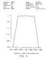
- FIG. 3is a graph of transmittance versus wavelength for a thin film filter having 160 layers of film made according to the present invention, where transmittance is shown on a scale between ⁇ 0.5 dB and zero dB;
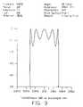
- FIG. 4is a graph of transmittance versus wavelength for the thin film filter of FIG. 3 , where transmittance is shown on a scale between ⁇ 25 dB and zero dB;
- FIG. 5is a graph of transmittance versus wavelength for a conventional tantalum oxide thin film filter having 180 film layers, where transmittance is shown on a scale between ⁇ 0.5 dB and zero dB;
- FIG. 6is a graph of transmittance versus wavelength for the thin film filter of FIG. 5 , where transmittance is shown on a scale between ⁇ 25 dB and zero dB.
- a thin film filter for dense wavelength division multiplexing in accordance with the present inventioncomprises a glass substrate 11 and a film stack 12 .
- the film stack 12comprises five cavities 13 , and is deposited on the glass substrate 11 .
- each cavity 13comprises a first group of mirror layers 21 , a second group of mirror layers 22 , and a spacer layer 23 between the first and second groups of mirror layers 21 , 22 .
- the structure of each cavity 13is (HL) m H(xL)H(LH) m C, where m is an integer and x is an even number.
- the symbol Hrepresents a high refractive index film.
- the symbol Lrepresents a low refractive index film.
- the symbol Crepresents a coupling film 24 that adjoins an adjacent cavity 13 .
- the coupling film 24is normally made of a material having a relative low refractive index. Values of m and of x in any one cavity 13 may be different from values of m and of x in any other cavity 13 .
- Each group of mirror layers 21 , 22comprises a plurality of high refractive index thin films 31 and a plurality of low refractive index thin films 32 .
- the high and low refractive index films 31 , 32are alternately deposited one on another.
- the structure of each group of mirror layers 21 , 22is (HL) m and (LH) m respectively, where m is an integer.
- a thickness of each high refractive index film 31 and of each low refractive index film 32is equal to a quarter of the central wavelength of a pass bandwidth of the thin film filter.
- the number of cavities of a thin film filteris key to determining its pass band shape, while the reflectivity of its groups of mirror layers determine the transmittance of the thin film filter.
- the first parameteris the number of films in each group of mirror layers.
- the second parameteris the difference between the refractive indices of the high refractive index films and the low refractive index films within each group of mirror layers.
- the material of the low refractive index films Lcan be silicon dioxide (SiO 2 ) or aluminum oxide (Al 2 O 3 ). In the preferred embodiment, silicon dioxide is used. Silicon dioxide has a refractive index of 1.46.
- the material of the high refractive index films His a composition of indium-tin oxide (ITO). The range of composition of the ITO material used is from 20% indium oxide plus 80% tin oxide to 17% indium oxide plus 83% tin oxide.
- ITOis used as the material of the high refractive index films 31 because it has a refractive index of 2.1. This is higher than the refractive index of materials conventionally used in high refractive index films; such as, tantalum pentoxide, which has a refractive index of 2.0. Thus a desired reflectivity can be attained using fewer films. ITO also has a special advantage when used in thin films. It is particularly soft and flexible, and more resistant to internal stress in the film layers compared to conventional materials.
- each spacer layer 23is H(xL)H, where x is an even number.
- the optical thickness of each low refractive index film 32is equal to a quarter of the central wavelength of the pass bandwidth of the thin film filter. Accordingly, a low refractive index layer 33 of the spacer layer 23 has an optical thickness equal to x times a quarter of the central wavelength of the pass bandwidth of the thin film filter.
- the optical thickness of each high refractive index film 31is equal to a quarter of the central wavelength of the pass bandwidth of the thin film filter. Accordingly, the spacer layer 23 has an optical thickness equal to x+2 times a quarter of the central wavelength of the pass bandwidth of the thin film filter.
- the substrate 11is transparent to wavelengths under which the thin film filter operates.
- the substrate 11may be made from a wide variety of materials including glass, quartz, optical plastic, silicon, and germanium.
- a thin film filter which has 160 layers of filmcan be produced according to the preferred embodiment.
- This thin film filterattains the same or better optical characteristics compared to a conventional DWDM thin film filter having 180 layers of film.
- the thin film filter of the present inventionhas a narrower pass bandwidth (1.028 nm at 25 dB and 0.644 nm at 0.5 dB) than that of the conventional thin film filter (1.066 nm at 25 dB and 0.644 nm at 0.5 dB).
- the thin film filter of the present inventionyields a waveform closer to an ideal square waveform.
Landscapes
- Physics & Mathematics (AREA)
- General Physics & Mathematics (AREA)
- Optics & Photonics (AREA)
- Optical Filters (AREA)
- Laminated Bodies (AREA)
Abstract
Description
Claims (11)
Priority Applications (3)
| Application Number | Priority Date | Filing Date | Title |
|---|---|---|---|
| US10/044,268US7019906B2 (en) | 2002-01-08 | 2002-01-08 | Indium-tin oxide thin film filter for dense wavelength division multiplexing |
| CNB021196060ACN1271427C (en) | 2002-01-08 | 2002-05-11 | thin film filter |
| TW091110314ATW565711B (en) | 2002-01-08 | 2002-05-17 | Indium-tin oxide thin film filter for dense wavelength division multiplexing |
Applications Claiming Priority (1)
| Application Number | Priority Date | Filing Date | Title |
|---|---|---|---|
| US10/044,268US7019906B2 (en) | 2002-01-08 | 2002-01-08 | Indium-tin oxide thin film filter for dense wavelength division multiplexing |
Publications (2)
| Publication Number | Publication Date |
|---|---|
| US20030128430A1 US20030128430A1 (en) | 2003-07-10 |
| US7019906B2true US7019906B2 (en) | 2006-03-28 |
Family
ID=21931420
Family Applications (1)
| Application Number | Title | Priority Date | Filing Date |
|---|---|---|---|
| US10/044,268Expired - Fee RelatedUS7019906B2 (en) | 2002-01-08 | 2002-01-08 | Indium-tin oxide thin film filter for dense wavelength division multiplexing |
Country Status (3)
| Country | Link |
|---|---|
| US (1) | US7019906B2 (en) |
| CN (1) | CN1271427C (en) |
| TW (1) | TW565711B (en) |
Cited By (7)
| Publication number | Priority date | Publication date | Assignee | Title |
|---|---|---|---|---|
| US20080151361A1 (en)* | 2005-03-29 | 2008-06-26 | Asml Netherlands B.V. | Multi-layer spectral purity filter, lithographic apparatus including such a spectral purity filter, device manufacturing method, and device manufactured thereby |
| US9022583B2 (en) | 2013-01-28 | 2015-05-05 | Gentex Corporation | Vehicular exterior transflective rearview mirror assembly |
| USD804377S1 (en) | 2016-10-27 | 2017-12-05 | Gentex Corporation | Rearview assembly |
| USD804376S1 (en) | 2016-10-27 | 2017-12-05 | Gentex Corporation | Rearview assembly |
| USD823204S1 (en) | 2016-12-16 | 2018-07-17 | Gentex Corporation | Outside rearview assembly with turn signal |
| USD830260S1 (en) | 2017-01-03 | 2018-10-09 | Gentex Corporation | External rearview mirror |
| USD837112S1 (en) | 2017-01-03 | 2019-01-01 | Gentex Corporation | Side view mirror electro optic device with blind spot indicator portion |
Families Citing this family (17)
| Publication number | Priority date | Publication date | Assignee | Title |
|---|---|---|---|---|
| US20050231800A1 (en)* | 2001-12-21 | 2005-10-20 | Barret Lippey | Selective reflecting |
| US6847483B2 (en)* | 2001-12-21 | 2005-01-25 | Bose Corporation | Selective reflecting |
| US7515336B2 (en)* | 2001-12-21 | 2009-04-07 | Bose Corporation | Selective reflecting |
| US7520624B2 (en)* | 2001-12-21 | 2009-04-21 | Bose Corporation | Light enhancing |
| US7170481B2 (en) | 2003-07-02 | 2007-01-30 | Kent Displays Incorporated | Single substrate liquid crystal display |
| WO2005072455A2 (en) | 2004-01-28 | 2005-08-11 | Kent Displays Incorporated | Drapable liquid crystal transfer display films |
| US20060042929A1 (en)* | 2004-08-26 | 2006-03-02 | Daniele Mauri | Method for reactive sputter deposition of an ultra-thin metal oxide film |
| US7517091B2 (en)* | 2005-05-12 | 2009-04-14 | Bose Corporation | Color gamut improvement in presence of ambient light |
| CN100419471C (en)* | 2005-08-02 | 2008-09-17 | 中山大学 | A Multi-frequency Acute Angle Spatial Filter |
| CN100386655C (en)* | 2005-10-27 | 2008-05-07 | 亚洲光学股份有限公司 | Three-channel optical filter |
| US20080037127A1 (en)* | 2006-03-31 | 2008-02-14 | 3M Innovative Properties Company | Wide angle mirror system |
| US8081368B2 (en) | 2007-03-29 | 2011-12-20 | Bose Corporation | Selective absorbing |
| DE102007025600B4 (en)* | 2007-05-31 | 2009-05-28 | Schott Ag | Interference filter and method for its production |
| CN103466538B (en)* | 2013-09-10 | 2016-01-20 | 中国航天科工集团第三研究院第八三五八研究所 | A kind of infrared with millimeter wave frequency division micro nano structure thin-film device |
| CN108957612A (en)* | 2018-07-26 | 2018-12-07 | 北极光电(深圳)有限公司 | A kind of film filter component and preparation method thereof |
| CN110632697B (en)* | 2019-09-24 | 2021-10-08 | 杭州灯之塔科技有限公司 | Polarizing element and preparation method thereof |
| CN113820775B (en)* | 2021-10-20 | 2025-08-08 | 信阳舜宇光学有限公司 | Optical filter and preparation method thereof |
Citations (6)
| Publication number | Priority date | Publication date | Assignee | Title |
|---|---|---|---|---|
| US4846551A (en)* | 1986-04-21 | 1989-07-11 | Optical Coating Laboratory, Inc. | Optical filter assembly for enhancement of image contrast and glare reduction of cathode ray display tube |
| US5321539A (en)* | 1991-02-04 | 1994-06-14 | Nippon Telegraph And Telephone Corporation | Liquid crystal Fabry-Perot etalon with glass spacer |
| US5914804A (en)* | 1998-01-28 | 1999-06-22 | Lucent Technologies Inc | Double-cavity micromechanical optical modulator with plural multilayer mirrors |
| US6042752A (en)* | 1997-02-21 | 2000-03-28 | Asahi Glass Company Ltd. | Transparent conductive film, sputtering target and transparent conductive film-bonded substrate |
| US6215592B1 (en)* | 1998-03-19 | 2001-04-10 | Ciena Corporation | Fabry-perot optical filter and method of making the same |
| US6490381B1 (en)* | 2000-06-01 | 2002-12-03 | Optical Coating Laboratory, Inc. | Fabry-Perot optical switch |
- 2002
- 2002-01-08USUS10/044,268patent/US7019906B2/ennot_activeExpired - Fee Related
- 2002-05-11CNCNB021196060Apatent/CN1271427C/ennot_activeExpired - Fee Related
- 2002-05-17TWTW091110314Apatent/TW565711B/ennot_activeIP Right Cessation
Patent Citations (6)
| Publication number | Priority date | Publication date | Assignee | Title |
|---|---|---|---|---|
| US4846551A (en)* | 1986-04-21 | 1989-07-11 | Optical Coating Laboratory, Inc. | Optical filter assembly for enhancement of image contrast and glare reduction of cathode ray display tube |
| US5321539A (en)* | 1991-02-04 | 1994-06-14 | Nippon Telegraph And Telephone Corporation | Liquid crystal Fabry-Perot etalon with glass spacer |
| US6042752A (en)* | 1997-02-21 | 2000-03-28 | Asahi Glass Company Ltd. | Transparent conductive film, sputtering target and transparent conductive film-bonded substrate |
| US5914804A (en)* | 1998-01-28 | 1999-06-22 | Lucent Technologies Inc | Double-cavity micromechanical optical modulator with plural multilayer mirrors |
| US6215592B1 (en)* | 1998-03-19 | 2001-04-10 | Ciena Corporation | Fabry-perot optical filter and method of making the same |
| US6490381B1 (en)* | 2000-06-01 | 2002-12-03 | Optical Coating Laboratory, Inc. | Fabry-Perot optical switch |
Cited By (8)
| Publication number | Priority date | Publication date | Assignee | Title |
|---|---|---|---|---|
| US20080151361A1 (en)* | 2005-03-29 | 2008-06-26 | Asml Netherlands B.V. | Multi-layer spectral purity filter, lithographic apparatus including such a spectral purity filter, device manufacturing method, and device manufactured thereby |
| US7639418B2 (en) | 2005-03-29 | 2009-12-29 | Asml Netherlands B.V. | Multi-layer spectral purity filter, lithographic apparatus including such a spectral purity filter, device manufacturing method, and device manufactured thereby |
| US9022583B2 (en) | 2013-01-28 | 2015-05-05 | Gentex Corporation | Vehicular exterior transflective rearview mirror assembly |
| USD804377S1 (en) | 2016-10-27 | 2017-12-05 | Gentex Corporation | Rearview assembly |
| USD804376S1 (en) | 2016-10-27 | 2017-12-05 | Gentex Corporation | Rearview assembly |
| USD823204S1 (en) | 2016-12-16 | 2018-07-17 | Gentex Corporation | Outside rearview assembly with turn signal |
| USD830260S1 (en) | 2017-01-03 | 2018-10-09 | Gentex Corporation | External rearview mirror |
| USD837112S1 (en) | 2017-01-03 | 2019-01-01 | Gentex Corporation | Side view mirror electro optic device with blind spot indicator portion |
Also Published As
| Publication number | Publication date |
|---|---|
| CN1432827A (en) | 2003-07-30 |
| TW565711B (en) | 2003-12-11 |
| CN1271427C (en) | 2006-08-23 |
| US20030128430A1 (en) | 2003-07-10 |
Similar Documents
| Publication | Publication Date | Title |
|---|---|---|
| US7019906B2 (en) | Indium-tin oxide thin film filter for dense wavelength division multiplexing | |
| CN100501452C (en) | Multiple Bandpass Filters | |
| JP4404568B2 (en) | Infrared cut filter and manufacturing method thereof | |
| CA2254679C (en) | Multilayer thin film dielectric bandpass filter | |
| JP3332879B2 (en) | Dichroic mirror | |
| US20100188737A1 (en) | Dielectric multilayer filter | |
| EP1258745A2 (en) | Optical filter | |
| WO1999036811A1 (en) | Optical interference filter | |
| US6407863B1 (en) | Dual transmission band interference filter | |
| JP2000329933A (en) | Multilayered film filter | |
| US20060245056A1 (en) | Thin-film structure with counteracting layer | |
| US20040080830A1 (en) | Niobium oxide and silicon dioxide thin film filter for dense wavelength division multiplexing | |
| CN111290064A (en) | Polarization-independent optical filter | |
| CN1417617A (en) | Intelligent film filter | |
| CN100371742C (en) | CWDM filter with four channels | |
| JPH0875902A (en) | Multi-layer antireflection film | |
| US7315420B2 (en) | CWDM filter with four channels | |
| CN112130243B (en) | Optical filter with linearly-changed transmittance | |
| CN100446447C (en) | thin film filter | |
| JP7251099B2 (en) | Bandpass filter and manufacturing method thereof | |
| EP1088248A1 (en) | Dual transmission band interference filter | |
| JPH0756004A (en) | Conductive antireflection film | |
| CN116990887B (en) | A membrane structure and its manufacturing method | |
| JP2005266039A (en) | Optical bandpass filter | |
| CN1601949A (en) | Dielectric film type dense wavelength division multiplexer filter |
Legal Events
| Date | Code | Title | Description |
|---|---|---|---|
| AS | Assignment | Owner name:HON HAI PRECISION IND., CO., LTD., TAIWAN Free format text:ASSIGNMENT OF ASSIGNORS INTEREST;ASSIGNORS:LEU, CHARLES;CHEN, GA-LANE;REEL/FRAME:012484/0477 Effective date:20011123 | |
| FPAY | Fee payment | Year of fee payment:4 | |
| AS | Assignment | Owner name:GOLD CHARM LIMITED, SAMOA Free format text:ASSIGNMENT OF ASSIGNORS INTEREST;ASSIGNOR:HON HAI PRECISION INDUSTRY CO., LTD.;REEL/FRAME:029576/0033 Effective date:20121227 | |
| FPAY | Fee payment | Year of fee payment:8 | |
| AS | Assignment | Owner name:GOOGLE INC., CALIFORNIA Free format text:ASSIGNMENT OF ASSIGNORS INTEREST;ASSIGNORS:HON HAI PRECISION INDUSTRY CO., LTD;GOLD CHARM LIMITED;HONG FUJIN PRECISION INDUSTRIAL (SHENZHEN) CO.;REEL/FRAME:032743/0832 Effective date:20140228 | |
| AS | Assignment | Owner name:GOOGLE LLC, CALIFORNIA Free format text:CHANGE OF NAME;ASSIGNOR:GOOGLE INC.;REEL/FRAME:044142/0357 Effective date:20170929 | |
| FEPP | Fee payment procedure | Free format text:MAINTENANCE FEE REMINDER MAILED (ORIGINAL EVENT CODE: REM.) | |
| LAPS | Lapse for failure to pay maintenance fees | Free format text:PATENT EXPIRED FOR FAILURE TO PAY MAINTENANCE FEES (ORIGINAL EVENT CODE: EXP.) | |
| STCH | Information on status: patent discontinuation | Free format text:PATENT EXPIRED DUE TO NONPAYMENT OF MAINTENANCE FEES UNDER 37 CFR 1.362 | |
| FP | Expired due to failure to pay maintenance fee | Effective date:20180328 |