US7019605B2 - Stacked bulk acoustic resonator band-pass filter with controllable pass bandwidth - Google Patents
Stacked bulk acoustic resonator band-pass filter with controllable pass bandwidthDownload PDFInfo
- Publication number
- US7019605B2 US7019605B2US10/699,289US69928903AUS7019605B2US 7019605 B2US7019605 B2US 7019605B2US 69928903 AUS69928903 AUS 69928903AUS 7019605 B2US7019605 B2US 7019605B2
- Authority
- US
- United States
- Prior art keywords
- acoustic
- fbars
- band
- pass filter
- decoupling material
- Prior art date
- Legal status (The legal status is an assumption and is not a legal conclusion. Google has not performed a legal analysis and makes no representation as to the accuracy of the status listed.)
- Expired - Lifetime, expires
Links
- 239000000463materialSubstances0.000claimsabstractdescription169
- 239000010410layerSubstances0.000claimsabstractdescription102
- 230000008878couplingEffects0.000claimsabstractdescription17
- 238000010168coupling processMethods0.000claimsabstractdescription17
- 238000005859coupling reactionMethods0.000claimsabstractdescription17
- 239000004033plasticSubstances0.000claimsabstractdescription14
- 239000002356single layerSubstances0.000claimsabstractdescription6
- 239000004642PolyimideSubstances0.000claimsdescription16
- 229920001721polyimidePolymers0.000claimsdescription16
- 238000000034methodMethods0.000claimsdescription13
- 229920000052poly(p-xylylene)Polymers0.000claimsdescription10
- -1poly(para-xylylene)Polymers0.000claimsdescription6
- 238000001914filtrationMethods0.000claimsdescription5
- 229910052751metalInorganic materials0.000description22
- 239000002184metalSubstances0.000description22
- ZOKXTWBITQBERF-UHFFFAOYSA-NMolybdenumChemical compound[Mo]ZOKXTWBITQBERF-UHFFFAOYSA-N0.000description15
- 229910052750molybdenumInorganic materials0.000description15
- 239000011733molybdenumSubstances0.000description15
- VYPSYNLAJGMNEJ-UHFFFAOYSA-NSilicium dioxideChemical compoundO=[Si]=OVYPSYNLAJGMNEJ-UHFFFAOYSA-N0.000description14
- 238000004544sputter depositionMethods0.000description12
- 238000001312dry etchingMethods0.000description8
- 238000004519manufacturing processMethods0.000description8
- 239000000377silicon dioxideSubstances0.000description7
- 239000000758substrateSubstances0.000description7
- KWYUFKZDYYNOTN-UHFFFAOYSA-MPotassium hydroxideChemical compound[OH-].[K+]KWYUFKZDYYNOTN-UHFFFAOYSA-M0.000description6
- 239000003870refractory metalSubstances0.000description6
- 238000004528spin coatingMethods0.000description6
- PMHQVHHXPFUNSP-UHFFFAOYSA-Mcopper(1+);methylsulfanylmethane;bromideChemical compoundBr[Cu].CSCPMHQVHHXPFUNSP-UHFFFAOYSA-M0.000description5
- 239000010408filmSubstances0.000description5
- XLOMVQKBTHCTTD-UHFFFAOYSA-NZinc monoxideChemical compound[Zn]=OXLOMVQKBTHCTTD-UHFFFAOYSA-N0.000description4
- 238000003780insertionMethods0.000description4
- 230000037431insertionEffects0.000description4
- 239000005360phosphosilicate glassSubstances0.000description4
- 239000010409thin filmSubstances0.000description4
- 230000015556catabolic processEffects0.000description3
- 230000001413cellular effectEffects0.000description3
- 238000006731degradation reactionMethods0.000description3
- 238000002955isolationMethods0.000description3
- ZAMOUSCENKQFHK-UHFFFAOYSA-NChlorine atomChemical compound[Cl]ZAMOUSCENKQFHK-UHFFFAOYSA-N0.000description2
- KRHYYFGTRYWZRS-UHFFFAOYSA-NFluoraneChemical compoundFKRHYYFGTRYWZRS-UHFFFAOYSA-N0.000description2
- GWEVSGVZZGPLCZ-UHFFFAOYSA-NTitan oxideChemical compoundO=[Ti]=OGWEVSGVZZGPLCZ-UHFFFAOYSA-N0.000description2
- 239000000460chlorineSubstances0.000description2
- 229910052801chlorineInorganic materials0.000description2
- 239000000470constituentSubstances0.000description2
- 238000005530etchingMethods0.000description2
- 230000001788irregularEffects0.000description2
- HFGPZNIAWCZYJU-UHFFFAOYSA-Nlead zirconate titanateChemical compound[O-2].[O-2].[O-2].[O-2].[O-2].[Ti+4].[Zr+4].[Pb+2]HFGPZNIAWCZYJU-UHFFFAOYSA-N0.000description2
- 238000004518low pressure chemical vapour depositionMethods0.000description2
- 239000000725suspensionSubstances0.000description2
- 238000001771vacuum depositionMethods0.000description2
- 238000001039wet etchingMethods0.000description2
- 239000011787zinc oxideSubstances0.000description2
- RTAQQCXQSZGOHL-UHFFFAOYSA-NTitaniumChemical compound[Ti]RTAQQCXQSZGOHL-UHFFFAOYSA-N0.000description1
- 238000000151depositionMethods0.000description1
- 230000008021depositionEffects0.000description1
- 238000005137deposition processMethods0.000description1
- 239000000539dimerSubstances0.000description1
- 239000007772electrode materialSubstances0.000description1
- 238000001704evaporationMethods0.000description1
- 230000008020evaporationEffects0.000description1
- PCHJSUWPFVWCPO-UHFFFAOYSA-NgoldChemical compound[Au]PCHJSUWPFVWCPO-UHFFFAOYSA-N0.000description1
- 239000010931goldSubstances0.000description1
- 229910052737goldInorganic materials0.000description1
- ORUIBWPALBXDOA-UHFFFAOYSA-Lmagnesium fluorideChemical compound[F-].[F-].[Mg+2]ORUIBWPALBXDOA-UHFFFAOYSA-L0.000description1
- 229910001635magnesium fluorideInorganic materials0.000description1
- 229910021421monocrystalline siliconInorganic materials0.000description1
- 229910052758niobiumInorganic materials0.000description1
- 239000010955niobiumSubstances0.000description1
- GUCVJGMIXFAOAE-UHFFFAOYSA-Nniobium atomChemical compound[Nb]GUCVJGMIXFAOAE-UHFFFAOYSA-N0.000description1
- 239000002245particleSubstances0.000description1
- 238000000059patterningMethods0.000description1
- 238000000206photolithographyMethods0.000description1
- 229920002120photoresistant polymerPolymers0.000description1
- 229920003223poly(pyromellitimide-1,4-diphenyl ether)Polymers0.000description1
- 239000002243precursorSubstances0.000description1
- 239000011241protective layerSubstances0.000description1
- 235000012239silicon dioxideNutrition0.000description1
- 239000010936titaniumSubstances0.000description1
- 229910052719titaniumInorganic materials0.000description1
- 239000004408titanium dioxideSubstances0.000description1
- WFKWXMTUELFFGS-UHFFFAOYSA-NtungstenChemical compound[W]WFKWXMTUELFFGS-UHFFFAOYSA-N0.000description1
- 229910052721tungstenInorganic materials0.000description1
- 239000010937tungstenSubstances0.000description1
Images


Classifications
- H—ELECTRICITY
- H03—ELECTRONIC CIRCUITRY
- H03H—IMPEDANCE NETWORKS, e.g. RESONANT CIRCUITS; RESONATORS
- H03H9/00—Networks comprising electromechanical or electro-acoustic elements; Electromechanical resonators
- H03H9/46—Filters
- H03H9/54—Filters comprising resonators of piezoelectric or electrostrictive material
- H03H9/58—Multiple crystal filters
- H03H9/582—Multiple crystal filters implemented with thin-film techniques
- H03H9/586—Means for mounting to a substrate, i.e. means constituting the material interface confining the waves to a volume
- H03H9/587—Air-gaps
- H—ELECTRICITY
- H03—ELECTRONIC CIRCUITRY
- H03H—IMPEDANCE NETWORKS, e.g. RESONANT CIRCUITS; RESONATORS
- H03H9/00—Networks comprising electromechanical or electro-acoustic elements; Electromechanical resonators
- H03H9/02—Details
- H03H9/125—Driving means, e.g. electrodes, coils
- H03H9/13—Driving means, e.g. electrodes, coils for networks consisting of piezoelectric or electrostrictive materials
- H03H9/132—Driving means, e.g. electrodes, coils for networks consisting of piezoelectric or electrostrictive materials characterized by a particular shape
- H—ELECTRICITY
- H03—ELECTRONIC CIRCUITRY
- H03H—IMPEDANCE NETWORKS, e.g. RESONANT CIRCUITS; RESONATORS
- H03H9/00—Networks comprising electromechanical or electro-acoustic elements; Electromechanical resonators
- H03H9/46—Filters
- H03H9/54—Filters comprising resonators of piezoelectric or electrostrictive material
- H03H9/58—Multiple crystal filters
- H03H9/582—Multiple crystal filters implemented with thin-film techniques
- H03H9/583—Multiple crystal filters implemented with thin-film techniques comprising a plurality of piezoelectric layers acoustically coupled
- H03H9/584—Coupled Resonator Filters [CFR]
- H—ELECTRICITY
- H03—ELECTRONIC CIRCUITRY
- H03H—IMPEDANCE NETWORKS, e.g. RESONANT CIRCUITS; RESONATORS
- H03H9/00—Networks comprising electromechanical or electro-acoustic elements; Electromechanical resonators
- H03H9/46—Filters
- H03H9/54—Filters comprising resonators of piezoelectric or electrostrictive material
- H03H9/58—Multiple crystal filters
- H03H9/60—Electric coupling means therefor
- H03H9/605—Electric coupling means therefor consisting of a ladder configuration
- Y—GENERAL TAGGING OF NEW TECHNOLOGICAL DEVELOPMENTS; GENERAL TAGGING OF CROSS-SECTIONAL TECHNOLOGIES SPANNING OVER SEVERAL SECTIONS OF THE IPC; TECHNICAL SUBJECTS COVERED BY FORMER USPC CROSS-REFERENCE ART COLLECTIONS [XRACs] AND DIGESTS
- Y10—TECHNICAL SUBJECTS COVERED BY FORMER USPC
- Y10T—TECHNICAL SUBJECTS COVERED BY FORMER US CLASSIFICATION
- Y10T29/00—Metal working
- Y10T29/42—Piezoelectric device making
- Y—GENERAL TAGGING OF NEW TECHNOLOGICAL DEVELOPMENTS; GENERAL TAGGING OF CROSS-SECTIONAL TECHNOLOGIES SPANNING OVER SEVERAL SECTIONS OF THE IPC; TECHNICAL SUBJECTS COVERED BY FORMER USPC CROSS-REFERENCE ART COLLECTIONS [XRACs] AND DIGESTS
- Y10—TECHNICAL SUBJECTS COVERED BY FORMER USPC
- Y10T—TECHNICAL SUBJECTS COVERED BY FORMER US CLASSIFICATION
- Y10T29/00—Metal working
- Y10T29/49—Method of mechanical manufacture
- Y10T29/49002—Electrical device making
- Y10T29/49005—Acoustic transducer
- Y—GENERAL TAGGING OF NEW TECHNOLOGICAL DEVELOPMENTS; GENERAL TAGGING OF CROSS-SECTIONAL TECHNOLOGIES SPANNING OVER SEVERAL SECTIONS OF THE IPC; TECHNICAL SUBJECTS COVERED BY FORMER USPC CROSS-REFERENCE ART COLLECTIONS [XRACs] AND DIGESTS
- Y10—TECHNICAL SUBJECTS COVERED BY FORMER USPC
- Y10T—TECHNICAL SUBJECTS COVERED BY FORMER US CLASSIFICATION
- Y10T29/00—Metal working
- Y10T29/49—Method of mechanical manufacture
- Y10T29/49002—Electrical device making
- Y10T29/49117—Conductor or circuit manufacturing
Definitions
- Electrical band-pass filtersare used in many different types of consumer and industrial electronic product to select or reject electrical signals in a range of frequencies.
- the physical size of such productshas tended to decrease significantly while the circuit complexity of the products has tended to increase. Consequently, a need for highly miniaturized, high-performance band-pass filters exists.
- a special need for such band-pass filtersexists in cellular telephones in which the antenna is connected to the output of the transmitter and the input of the receiver through a duplexer that includes two band-pass filters.
- each of the band-pass filtersincludes a ladder circuit in which each element of the ladder circuit is a film bulk acoustic resonator (FBAR).
- FBARfilm bulk acoustic resonator
- Such a duplexeris disclosed by Bradley et al. in U.S. Pat. No. 6,262,637 entitled Duplexer Incorporating Thin-film Bulk Acoustic Resonators (FBARs), assigned to the assignee of this disclosure and incorporated into this disclosure by reference.
- Such duplexeris composed of a transmitter band-pass filter connected in series between the output of the transmitter and the antenna and a receiver band-pass filter connected in series with 90° phase-shifter between the antenna and the input of the receiver. The center frequencies of the pass-bands of the transmitter band-pass filter and the receiver band-pass filter are offset from one another.
- FIG. 1shows an exemplary embodiment of an FBAR-based band-pass filter 10 suitable for use as the transmitter band-pass filter of a duplexer.
- the transmitter band-pass filteris composed of series FBARs 12 and shunt FBARs 14 connected in a ladder circuit.
- Series FBARs 12have a higher resonant frequency than shunt FBARs 14 .
- FIG. 2shows an exemplary embodiment 20 of an FBAR.
- FBAR 20is composed a pair of electrodes 24 and 26 and a layer of piezoelectric material 22 sandwiched between the electrodes.
- the piezoelectric material and electrodesare suspended over a cavity 28 defined in a substrate 30 .
- This way of suspending the FBARallows the FBAR to resonate mechanically in response to an electrical signal applied between the electrodes.
- Other suspension schemes that allow the FBAR to resonate mechanicallyare possible.
- FIG. 3shows an exemplary embodiment 40 of the SBAR disclosed in U.S. Pat. No. 5,587,620.
- SBAR 40is composed of two layers 22 , 42 of piezoelectric material interleaved with three electrodes 24 , 26 , 44 .
- An input electrical signalis applied between electrodes 44 and 26 and an output electrical signal is provided between electrodes 24 and 26 .
- the center electrode 26is common to both the input and the output.
- the SBAR disclosed in U.S. Pat. No. 5,587,620was thought to have promise for use as a band-pass filter because it has an inherent band-pass characteristic.
- practical examples of the SBARexhibit an extremely narrow pass bandwidth that makes the SBAR unsuitable for use in most band-pass filtering applications, including the cellular telephone duplexer application referred to above.
- the narrow pass bandwidth of the SBARcan be seen in FIG. 4 , which compares the frequency response of a practical example of SBAR 40 shown in FIG. 3 (curve 46 ) with the frequency response a practical example of the FBAR-based band-pass ladder filter shown in FIG. 1 (curve 48 ).
- FIG. 4also shows that, while the frequency response of the ladder filter shown in FIG. 1 advantageously falls sharply outside the pass-band, as the frequency difference from the center frequency further increases, the frequency response undesirably rises again.
- the inventionprovides in a first aspect a band-pass filter characterized by a center frequency.
- the band-pass filterhas a stacked pair of film bulk acoustic resonators (FBARs) and an acoustic decoupler between the FBARs.
- FBARsfilm bulk acoustic resonators
- Each of the FBARshas opposed planar electrodes and a layer of piezoelectric material between the electrodes.
- the acoustic decouplerhas a single layer of acoustic decoupling material having a nominal thickness equal to an odd integral multiple of one quarter of the wavelength in the acoustic decoupling material of an acoustic wave having a frequency equal to the center frequency.
- the acoustic decoupling materialcomprises plastic.
- the acoustic decouplercontrols the coupling of acoustic energy between the FBARs. Specifically, the acoustic decoupler couples less acoustic energy between the FBARs than would be coupled by direct contact between the FBARs as in the exemplary SBAR shown in FIG. 3 .
- the reduced acoustic couplinggives the band-pass filter such desirable properties as a low insertion loss and flat frequency response in its pass band, a pass bandwidth in the range from about 3% to about 5% of the center frequency and good out-of-band rejection.
- the acoustic decoupling materialhas an acoustic impedance less than that of the other materials of the FBARs.
- the inventionprovides a band-pass filter characterized by a center frequency.
- the band-pass filterhas a stacked pair of film bulk acoustic resonators (FBARs) and a single layer of acoustic decoupling material between the FBARs.
- FBARsfilm bulk acoustic resonators
- Each of the FBARshas opposed planar electrodes and a layer of piezoelectric material between the electrodes.
- the layer of acoustic decoupling materialhas a nominal thickness equal to an odd integral multiple of one quarter of the wavelength in the acoustic decoupling material of an acoustic wave having a frequency equal to the center frequency.
- the acoustic decoupling materialcomprises plastic having an acoustic impedance less than the acoustic impedance of the piezoelectric material.
- the inventionprovides an electrical filtering method.
- a pair of film bulk acoustic resonators (FBARs)is provided.
- An input electrical signalis applied to one of the FBARs.
- Acoustic energyis coupled between the FBARs by no more than one layer of acoustic decoupling material located between the FBARs.
- the acoustic decoupling materialcomprises plastic.
- the acoustic energy coupledis less than would be coupled by direct contact between the FBARs.
- a filtered output electrical signalis output from the other of the FBARs.
- FIG. 1is a schematic drawing of a band-pass filter incorporating FBARs.
- FIG. 2is a schematic side view of an FBAR.
- FIG. 3is a schematic side view of an SBAR.
- FIG. 4is a graph comparing the calculated frequency response of the SBAR shown in FIG. 3 and that of the FBAR-based band-pass filter shown in FIG. 1 .
- FIG. 5Ais a plan view of an example of a first embodiment of a band-pass filter in accordance with the invention.
- FIG. 5Bis a cross-sectional view of the band-pass filter shown in FIG. 5A along the section line 5 B— 5 B.
- FIG. 5Cis an enlarged cross-sectional view of part of the band-pass filter shown in FIG. 5A along the section line 5 B— 5 B showing a first embodiment of the acoustic decoupler.
- FIG. 5Dis an enlarged cross-sectional view of part of the band-pass filter shown in FIG. 5A along the section line 5 B— 5 B showing a second embodiment of the acoustic decoupler.
- FIG. 6is a graph comparing the calculated frequency responses of embodiments of the band-pass filter in accordance with the invention incorporating acoustic decouplers of acoustic decoupling materials having different acoustic impedances.
- FIGS. 7A–7Jare plan views illustrating a process for making a band-pass filter in accordance with the invention.
- FIGS. 7K–7Tare cross-sectional views along the section lines 7 K— 7 K, 7 L— 7 L, 7 M— 7 M, 7 N— 7 N, 7 O— 7 O, 7 P— 7 P, 7 Q— 7 Q, 7 R— 7 R, 7 S— 7 S and 7 T— 7 T in FIGS. 7A–7J , respectively.
- FIG. 8is a schematic drawing of an example of a second embodiment of a band-pass filter in accordance with the invention.
- FIG. 9is a graph comparing the calculated frequency response of the embodiment of the band-pass filter shown in FIG. 8 with the embodiment of the band-pass filter shown in FIGS. 5A and 5B .
- the SBAR shown in FIG. 3can be regarded as being composed of two FBARs, one stacked on top of the other.
- One of the FBARsis composed of piezoelectric layer 22 sandwiched between electrodes 24 and 26 .
- the other of the FBARsis composed of piezoelectric layer 42 sandwiched between electrodes 26 and 44 .
- Electrode 26 common to both FBARsprovides close coupling of acoustic energy between the FBARs. This results in the FBARs being acoustically highly over-coupled so that SBAR 40 exhibits the single Lorentzian resonance illustrated in curve 46 of FIG. 4 .
- the single Lorentzian resonancemakes it difficult or impossible to design a band-pass filter with such desirable characteristics such as broad pass band, a flat in-band frequency response and a sharp roll-off outside the pass band.
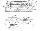
- FIG. 5Ais a schematic side view showing the structure of an exemplary embodiment 100 of a band-pass filter in accordance with the invention.
- FIG. 5Bis a cross-sectional view along the section line 5 B— 5 B in FIG. 5A .
- Band-pass filter 100is composed of a stacked pair of film bulk acoustic resonators (FBARs) 110 and 120 .
- FBAR 120is stacked atop FBAR 110 .
- FBAR 110is composed of opposed planar electrodes 112 and 114 and a layer 116 of piezoelectric material between the electrodes.
- FBAR 120is composed of opposed planar electrodes 122 and 124 and a layer 126 of piezoelectric material between the electrodes.
- Band-pass filter 100is also composed of an acoustic decoupler 130 between FBARs 110 and 120 , specifically, between electrodes 114 and 122 .
- the acoustic decouplercontrols the coupling of acoustic energy between FBARs 110 and 120 .
- the acoustic decouplercouples less acoustic energy between the FBARs than would be coupled by direct contact between the FBARs as in the exemplary SBAR shown in FIG. 3 .
- the stacked FBARs 110 and 120are suspended over a cavity 104 defined in a substrate 102 .
- This way of suspending the stacked FBARsallows the stacked FBARs to resonate mechanically in response to an input electrical signal applied between the electrodes of one of them.
- Other suspension schemes that allow the stacked FBARs to resonate mechanically in response to an input electrical signalare possible.
- the stacked FBARscan be located over a mismatched acoustic Bragg reflector (not shown) formed in or on substrate 102 , as disclosed by Lakin in U.S. Pat. No. 6,107,721, the disclosure of which is incorporated into this disclosure by reference.
- acoustic decoupler 130controls the acoustic coupling between FBARs 110 and 120 .
- the acoustic coupling provided by acoustic decoupler 130is substantially less than the acoustic coupling between the FBARs in the SBAR embodiment shown in FIG. 3 .
- FBARs 110 and 120are not over coupled, and band-pass filter 100 has a relatively broad and flat in-band response and a sharp roll-off outside the pass band instead of the single Lorentzian resonance shown in FIG. 4 (curve 46 ) of the over-coupled conventional SBAR.
- the frequency response of band-pass filter 100will be described further below with reference to FIG. 6 .
- FIG. 5Cis an enlarged view of a first embodiment of acoustic decoupler 130 in which the acoustic decoupler is composed of a layer 131 of acoustic decoupling material located between the electrodes 114 and 122 of FBARs 110 and 120 , respectively ( FIG. 5B ).
- Layer 131 of acoustic decoupling materialhas a nominal thickness that is an odd integral multiple of one quarter of the wavelength in the acoustic decoupling material of an acoustic wave having a frequency equal to the center frequency of band-pass filter 100 .
- the acoustic decoupling materialhas an acoustic impedance less than that of the piezoelectric material that constitutes the FBARs 110 , 120 .
- the acoustic decoupling materialadditionally has a high electrical resistivity and a low dielectric permittivity.
- the acoustic decoupling material of acoustic decoupler 130has an acoustic impedance less that of the piezoelectric material of FBARs 110 and 120 .
- the acoustic decoupling materialalso has an acoustic impedance substantially greater than that of air.
- the acoustic impedance of a materialis the ratio of stress to particle velocity in the material and is measured in Rayleighs, abbreviated as rayl.
- the piezoelectric material of layers 116 , 216 of the FBARsis typically aluminum nitride (AIN).
- the acoustic impedance of AINis typically about 35 Mrayl and that of molybdenum, a typical electrode material, is about 63 Mrayl.
- the acoustic impedance of airis about 1 krayl.
- materials with an acoustic impedance in the range from about 2 Mrayl to about 16 Mraylwork well as the acoustic decoupling material of layer 131 .
- FIG. 6shows how the calculated frequency response of band-pass filter 100 depends on the acoustic impedance of the acoustic decoupling material of layer 131 that constitutes an embodiment of acoustic decoupler 130 .
- the embodiment illustratedhas a center frequency of about 1,900 MHz.
- Calculated frequency responses for embodiments in which the acoustic decoupling material has an acoustic impedance of about 4 Mrayl, e.g., polyimide, (curve 140 ), about 8 Mrayl (curve 142 ) and about 16 Mrayl (curve 144 )are shown.
- the width of the passband of the band-pass filterincreases with increasing acoustic impedance of the acoustic decoupling material. Accordingly, by making an appropriate choice of the acoustic decoupling material, embodiments of band-pass filter 100 having a desired pass-band characteristic can be made.
- the embodiment in which the acoustic decoupling material of layer 131 is polyimideexhibits some under coupling of acoustic energy between FBARs 110 , 120 , but nevertheless has a pass band that is usefully wide.
- the embodiment in which the acoustic decoupling material has an acoustic impedance of about 8 Mraylexhibits near critical coupling of acoustic energy between FBARs 110 , 120 .
- the embodiment in which the acoustic impedance of the acoustic decoupling material is about 16 Mraylexhibits a double peak in the in-band response typical of significant over coupling of acoustic energy between FBARs 110 , 120 .
- An embodiment in which the acoustic decoupling material had an acoustic impedance intermediate between 4 Mrayl and 8 Mraylwould have an in-band response that included a flat portion indicative of critical coupling of acoustic energy between FBARs 110 , 120 .
- acoustic decoupling materialhas an acoustic impedance of 8 Mrayl or less have an insertion loss of less than 3 dB, and some embodiments have an insertion loss of less than 1 dB.
- the embodiment of acoustic decoupler 130 shown in FIG. 5Cis composed of layer 131 of acoustic decoupling material with a nominal thickness equal to one quarter of the wavelength in the acoustic decoupling material of an acoustic wave having a frequency equal to the center frequency of the band-pass filter, i.e., t ⁇ n /4, where t is the thickness of layer 131 and ⁇ n is the wavelength in the acoustic decoupling material of an acoustic wave having a frequency equal to the center frequency of band-pass filter 100 .
- a thickness of layer 131 within approximately ⁇ 10% of the nominal thicknesscan alternatively be used.
- a thickness outside this rangecan alternatively be used with some degradation in performance.
- the thickness of layer 131should differ significantly from 0 ⁇ n at one extreme (see FIG. 3 ) and ⁇ n /2 at the other extreme.
- the embodiment of acoustic decoupler 130 shown in FIG. 5Cis composed of layer 131 of acoustic decoupling material with a nominal thickness equal to an odd integral multiple of one quarter of the wavelength in the acoustic decoupling material of an acoustic wave having a frequency equal to the center frequency of band-pass filter 100 , i.e., t ⁇ (2m+1) ⁇ n /4, where t and ⁇ n are as defined above and m is an integer equal to or greater than zero.
- a thickness of layer 131 that differs from the nominal thickness by approximately ⁇ 10% of ⁇ n /4can alternatively be used. A thickness tolerance outside this range can be used with some degradation in performance, but the thickness of layer 131 should differ significantly from an integral multiple of ⁇ n /2.
- layer 131is formed by spin coating the acoustic decoupling material over electrode 114 .
- a layer formed by spin coatingwill typically have regions of different thickness due to the contouring of the surface coated by the acoustic decoupling material of layer 131 .
- the thickness of layer 131 of acoustic decoupling materialis the thickness of the portion of the layer located between electrodes 114 and 122 .
- plastic materialshave acoustic impedances in the range stated above and can be applied in layers of uniform thickness in the thickness ranges stated above. Such plastic materials are therefore potentially suitable for use as the acoustic decoupling material of layer 131 of acoustic decoupler 130 .
- the acoustic decoupling materialmust also be capable of withstanding the temperatures of the fabrication operations performed after layer 131 of acoustic decoupling material has been deposited on electrode 114 to form acoustic decoupler 130 .
- electrodes 122 and 124 and piezoelectric layer 126are deposited by sputtering after layer 131 has been deposited. Temperatures as high as 300° C. are reached during these deposition processes. Thus, a plastic that remains stable at such temperatures is used as the acoustic decoupling material.
- Plastic materialstypically have a very high acoustic attenuation per unit length compared with the other materials of FBARs 110 and 120 .
- acoustic decoupler 130is composed of layer 131 of plastic acoustic decoupling material typically less than 1 ⁇ m thick, the acoustic attenuation introduced by layer 131 of acoustic decoupling material is typically negligible.
- a polyimideis used as the acoustic decoupling material of layer 131 .
- Polyimideis sold under the trademark Kapton® by E. I. duPont de Nemours and Company.
- acoustic decoupler 130is composed of layer 131 of polyimide applied to electrode 114 by spin coating.
- Polyimidehas an acoustic impedance of about 4 Mrayl.
- a poly(para-xylylene)is used as the acoustic decoupling material of layer 131 .
- acoustic decoupler 130is composed of layer 131 of poly(para-xylylene) applied to electrode 114 by vacuum deposition.
- Poly(para-xylylene)is also known in the art as parylene.
- the dimer precursor di-para-xylylene from which parylene is made and equipment for performing vacuum deposition of layers of paryleneare available from many suppliers.
- Parylenehas an acoustic impedance of about 2.8 Mrayl.
- the acoustic decoupling material of layer 131 constituting acoustic decoupler 130has an acoustic impedance substantially greater than the materials of FBARs 110 and 120 . No materials having this property are known at this time, but such materials may become available in future, or lower acoustic impedance FBAR materials may become available in future.
- the thickness of layer 131 of such high acoustic impedance acoustic decoupling materialis as described above.
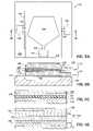
- FIG. 5Dis an enlarged view of part of band-pass filter 100 showing a second embodiment of acoustic decoupler 130 that incorporates a Bragg structure 161 .
- Bragg structure 161is composed of a low acoustic impedance Bragg element 163 sandwiched between high acoustic impedance Bragg elements 165 and 167 .
- Low acoustic impedance Bragg element 163is a layer of a low acoustic impedance material whereas high acoustic impedance Bragg elements 165 and 167 are each a layer of high acoustic impedance material.
- the acoustic impedances of the materials of the Bragg elementsare characterized as “low” and “high” with respect to one another and with respect to the acoustic impedance of the piezoelectric material of layers 116 and 126 .
- at least one of the Bragg elementsadditionally has a high electrical resistivity and a low dielectric permittivity.
- Each of the layers constituting Bragg elements 161 , 163 and 165has a nominal thickness equal to an odd integral multiple of one quarter of the wavelength in the material the layer of an acoustic wave having a frequency equal to the center frequency of band-pass filter 100 .
- Layers that differ from the nominal thickness by approximately ⁇ 10% of one quarter of the wavelengthcan alternatively be used. A thickness tolerance outside this range can be used with some degradation in performance, but the thickness of the layers should differ significantly from an integral multiple of one-half of the wavelength.
- low acoustic impedance Bragg element 163is a layer of silicon dioxide (SiO 2 ), which has an acoustic impedance of about 13 Mrayl
- each of the high acoustic impedance Bragg elements 165 and 167is a layer of the same material as electrodes 114 and 122 , respectively, i.e., molybdenum, which has an acoustic impedance of about 63 Mrayl.
- high acoustic impedance Bragg elements 165 and 167have a thickness of one quarter of the wavelength in molybdenum of an acoustic wave having a frequency equal to the center frequency of band-pass filter 100
- low acoustic impedance Bragg element 163has a thickness of three quarters of the wavelength in SiO 2 of an acoustic wave having a frequency equal to the center frequency of the band-pass filter.
- Using a three-quarter wavelength-thick layer of SiO 2 instead of a one-quarter wavelength thick layer of SiO 2 as low acoustic impedance Bragg element 163reduces the capacitance between FBARs 110 and 120 .
- Bragg structure 161may be composed of more than one (e.g., n) low acoustic impedance Bragg element interleaved with a corresponding number (i.e., n+1) of high acoustic impedance Bragg elements. Only one of the Bragg elements need be insulating.
- the Bragg structuremay be composed of two low acoustic impedance Bragg elements interleaved with three high acoustic impedance Bragg elements.
- Wafer-scale fabricationis used to fabricate thousands of band-pass filters similar to band-pass filter 100 at the same time. Such wafer-scale fabrication makes the band-pass filters inexpensive to fabricate.
- An exemplary fabrication methodwill be described next with reference to the plan views of FIGS. 7A–7J and the cross-sectional views of FIGS. 7K–7T .
- FIGS. 7A–7J and FIGS. 7K–7Tillustrate and the following description describes the fabrication of band-pass filter 100 in and on a portion of the wafer. As band-pass filter 100 is fabricated, the remaining band-pass filters on the wafer as similarly fabricated.
- the portion of the wafer that constitutes substrate 102 of band-pass filter 100is selectively wet etched to form cavity 104 , as shown in FIGS. 7A and 7K .
- FIGS. 7B and 7Lshow cavity 104 in substrate 102 filled with fill material 105 .
- the fill materialwas phosphosilicate glass (PSG) and was deposited using conventional low-pressure chemical vapor deposition (LPCVD).
- the fill materialmay alternatively be deposited by sputtering, or by spin coating.
- Electrode 112typically has an irregular shape in a plane parallel to the major surface of the wafer. An irregular shape minimizes lateral modes in the FBAR 110 of which it forms part, as described in U.S. Pat. No. 6,215,375 of Larson III et al., the disclosure of which is incorporated into this disclosure by reference. Electrode 112 is shaped and located to expose part of the surface of fill material 105 so that the fill material can later be removed by etching, as will be described below.
- electrodes 112 , 114 , 122 and 124FIG. 5B
- the metal layers in which electrodes 112 , 114 , 122 and 124 ( FIG. 5B ) are definedare patterned such that, in respective planes parallel to the major surface of the wafer, electrodes 112 and 114 have the same shape, size, orientation and position, electrodes 122 and 124 have the same shape, size, orientation and position, and electrodes 114 and 122 typically have the same shape, size, orientation and position.
- the metal deposited to form electrode 112 , bonding pad 132 and trace 133was molybdenum.
- the molybdenumwas deposited with a thickness of about 440 nm by sputtering, and was patterned by dry etching to define a pentagonal electrode with an area of about 26,000 square ⁇ m.
- Other refractory metalssuch as tungsten, niobium and titanium may alternatively be used as the material of electrode 112 , bonding pad 132 and trace 133 .
- the electrode, bonding pad and tracemay alternatively comprise layers of more than one material.
- a layer of piezoelectric materialis deposited and is patterned to define piezoelectric layer 116 as shown in FIGS. 7D and 7N .
- Piezoelectric layer 116is patterned to expose part of the surface of fill material 105 and bonding pad 132 of electrode 112 .
- Piezoelectric layer 116is additionally patterned to define windows 119 that provide access to additional parts of the surface of the fill material.
- the piezoelectric material deposited to form piezoelectric layer 116was aluminum nitride and was deposited with a thickness of about 780 nm by sputtering.
- the piezoelectric materialwas patterned by wet etching in potassium hydroxide or by chlorine-based dry etching.
- Alternative materials for piezoelectric layer 116include zinc oxide and lead zirconium titanate.
- a layer of metalis deposited and is patterned to define electrode 114 , a bonding pad 134 and an electrical trace 135 extending between electrode 114 and bonding pad 134 , as shown in FIGS. 7E and 7O .
- the metal deposited to form electrode 114was molybdenum.
- the molybdenumwas deposited with a thickness of about 440 nm by sputtering, and was patterned by dry etching.
- Other refractory metalsmay alternatively be used as the material of electrode 114 , bonding pad 134 and trace 135 .
- the electrode, bonding pad and tracemay alternatively comprise layers of more than one material.
- a layer of acoustic decoupling materialis then deposited and is patterned to define acoustic decoupler 130 , as shown in FIGS. 7F and 7P .
- Acoustic decoupler 130is shaped to cover at least electrode 114 , and is additionally shaped to expose part of the surface of fill material 105 and bonding pads 132 and 134 .
- Acoustic decoupler 130is additionally patterned to define windows 119 that provide access to additional parts of the surface of the fill material.
- the acoustic decoupling materialwas polyimide with a thickness of about 750 nm, i.e., three quarters of the center frequency wavelength in the polyimide.
- the polyimidewas deposited by spin coating, and was patterned by photolithography. Polyimide is photosensitive so that no photoresist is needed.
- other plastic materialscan be used as the acoustic decoupling material.
- the acoustic decoupling materialcan be deposited by methods other than spin coating.
- the waferwas baked at about 300° C. before further processing was performed.
- the bakeevaporates volatile constituents of the polyimide and prevents the evaporation of such volatile constituents during subsequent processing from causing subsequently-deposited layers to separate.
- a layer of metalis deposited and is patterned to define electrode 122 and an electrical trace 137 extending from electrode 122 to bonding pad 134 , as shown in FIGS. 7G and 7Q .
- Bonding pad 134is also electrically connected to electrode 114 by trace 135 .
- the metal deposited to form electrode 122was molybdenum.
- the molybdenumwas deposited with a thickness of about 440 nm by sputtering, and was patterned by dry etching.
- Other refractory metalsmay alternatively be used as the material of electrode 122 and trace 137 .
- the electrode and the tracemay alternatively comprise layers of more than one material.
- a layer of piezoelectric materialis deposited and is patterned to define piezoelectric layer 126 .
- Piezoelectric layer 126is shaped to expose bonding pads 132 and 134 and to expose part of the surface of fill material 105 as shown in FIGS. 7H and 7R .
- Piezoelectric layer 126is additionally patterned to define windows 119 that provide access to additional parts of the surface of the fill material.
- the piezoelectric material deposited to form piezoelectric layer 126was aluminum nitride and was deposited with a thickness of about 780 nm by sputtering.
- the piezoelectric materialwas patterned by wet etching in potassium hydroxide or by chlorine-based dry etching.
- Alternative materials for piezoelectric layer 126include zinc oxide and lead zirconium titanate.
- a layer of metalis deposited and is patterned to define electrode 124 , a bonding pad 138 and an electrical trace 139 extending from electrode 124 to bonding pad 138 , as shown in FIGS. 7I and 7S .
- the metal deposited to form electrode 124was molybdenum.
- the molybdenumwas deposited with a thickness of about 440 nm by sputtering, and was patterned by dry etching.
- Other refractory metalssuch may alternatively be used as the material of electrode 124 , bonding pad 138 and trace 139 .
- the electrode, bonding pad and tracemay alternatively comprise layers of more than one material.
- the waferis then isotropically wet etched to remove fill material 105 from cavity 104 . As noted above, portions of the surface of fill material 105 remain exposed through, for example, windows 119 . The etch process leaves band-pass filter 100 suspended over cavity 104 , as shown in FIGS. 7J and 7T .
- the etchant used to remove fill material 105was dilute hydrofluoric acid.
- a gold protective layeris deposited on the exposed surfaces of bonding pads 132 , 134 and 138 .
- band-pass filter 100The wafer is then divided into individual band-pass filters, including band-pass filter 100 .
- Each band-pass filteris mounted in a package and electrical connections are made between bonding pads 132 , 134 and 138 of the band-pass filter and pads that are part of the package.
- acoustic decoupler 130incorporates a Bragg structure, as shown in FIG. 5D , is made by a process similar to that described above. The process differs as follows:
- a layer of metalis deposited and is patterned to define high acoustic impedance Bragg element 165 shown in FIG. 5D , bonding pad 134 and electrical trace 135 extending between high acoustic impedance Bragg element 165 and bonding pad 134 , in a manner similar to that shown in FIGS. 7E and 7O .
- the layer of metalis deposited with a nominal thickness equal to an odd, integral multiple of one quarter of the wavelength in the metal of an acoustic wave having a frequency equal to the center frequency of band-pass filter 100 .
- High acoustic impedance Bragg element 165additionally serves as electrode 114 as shown in FIG. 5D .
- the metal deposited to form high acoustic impedance Bragg element 165is molybdenum.
- the molybdenumis deposited with a thickness of about 820 nm (one-quarter wavelength in Mo) by sputtering, and is patterned by dry etching.
- Other refractory metalsmay alternatively be used as the material of high acoustic impedance Bragg element 165 , bonding pad 134 and trace 135 .
- the high acoustic impedance Bragg element, bonding pad and tracemay alternatively comprise layers of more than one metal.
- a layer of low acoustic impedance materialis then deposited and is patterned to define low acoustic impedance Bragg element 163 in a manner similar to that shown in FIGS. 7F and 7P .
- the layer of low acoustic impedance materialis deposited with a nominal thickness equal to an odd, integral multiple of one quarter of the wavelength in the material of an acoustic wave having a frequency equal to the center frequency of band-pass filter 100 .
- Low acoustic impedance Bragg element 163is shaped to cover at least high acoustic impedance Bragg element 165 , and is additionally shaped to expose part of the surface of fill material 105 and bonding pads 132 and 134 .
- the layer of low acoustic impedance materialis additionally patterned to define windows 119 that provide access to additional parts of the surface of the fill material.
- the low acoustic impedance materialis SiO 2 with a thickness of about 790 nm.
- the SiO 2is deposited by sputtering, and is patterned by etching.
- Other low acoustic impedance material that can be used as the material of low acoustic impedance Bragg elementinclude phosphosilicate glass (PSG), titanium dioxide and magnesium fluoride.
- PSGphosphosilicate glass
- titanium dioxidetitanium dioxide
- magnesium fluoridemagnesium fluoride
- a layer of metalis deposited and is patterned to define high acoustic impedance Bragg element 167 shown in FIG. 5D and electrical trace 137 extending from high acoustic impedance Bragg element 167 to bonding pad 134 in a manner similar to that shown in FIGS. 7G and 7Q .
- Bonding pad 134is also electrically connected to high acoustic impedance Bragg element 167 by trace 135 .
- the layer of metalis deposited with a nominal thickness equal to an odd, integral multiple of one quarter of the wavelength in the metal of an acoustic wave having a frequency equal to the center frequency of band-pass filter 100 .
- High acoustic impedance Bragg element 167additionally serves as electrode 122 as shown in FIG. 5D .
- the metal deposited to form high acoustic impedance Bragg element 167 and electrical trace 137is molybdenum.
- the molybdenumis deposited with a thickness of about 820 nm (one-quarter wavelength in Mo) by sputtering, and is patterned by dry etching.
- Other refractory metalsmay alternatively be used as the material of high acoustic impedance Bragg element 167 and trace 137 .
- the high acoustic impedance Bragg element and the tracemay alternatively comprise layers of more than one material.
- a layer of piezoelectric materialis then deposited and is patterned to define piezoelectric layer 126 , as described above with reference to FIGS. 7H and 7R , and the process continues as described above to complete fabrication of band-pass filter 100 .
- Band-pass filter 100is used as follows. Bonding pad 134 electrically connected to electrodes 114 and 122 provides a ground terminal of the band-pass filter 100 , bonding pad 132 electrically connected to electrode 112 provides an input terminal of the band-pass filter 100 , and bonding pad 138 electrically connected to electrode 124 provides an output terminal of the band-pass filter 100 .
- the input terminal and the output terminalcan be interchanged.
- band-pass filter 100may additionally provide electrical isolation between input and output.
- an additional bonding pad(not shown) is defined in the metal in which electrode 122 and trace 137 are defined, and trace 137 extends from electrode 122 to the additional boding pad instead of to bonding pad 134 .
- Bonding pad 132 and 134 electrically connected to electrodes 112 and 114respectively, provide a pair of input terminals and the additional bonding pad (not shown) electrically connected by trace 137 to electrode 122 and bonding pad 138 electrically connected to electrode 124 provide a pair of output terminals.
- the input terminals and the output terminalsare electrically isolated from one another. Again, the input terminals and output terminals may be interchanged.
- FIG. 8is a schematic drawing of an exemplary embodiment 200 of a band-pass filter in accordance with the invention having an out-of-band frequency response that has a steeper slope than that of band-pass filter 100 , and in which, after the initial sharp fall, the frequency response rises to a substantially lower level than the band-pass ladder filter shown in FIG. 1 .
- Band-pass filter 200is composed of a simplified FBAR-based ladder filter 210 connected in series with band-pass filter 100 described above with reference to FIGS. 5A and 5B .
- Ladder filter 210is composed of series FBARs 212 and 214 and a shunt FBAR 216 .
- Series FBARs 212 and 214have a higher resonant frequency than shunt FBAR 214 .
- band-pass filter 100In band-pass filter 100 , electrode 112 is connected to ground, electrodes 114 and 122 are connected to the output of ladder filter 210 , i.e., to the electrode 218 of FBAR 214 , and electrode 124 provides the output terminal of band-pass filter 200 : FBARs 212 , 214 and 216 and band-pass filter 100 are structured so that band-pass filter 100 has a broader pass band than ladder filter 210 .
- FIG. 9is a graph showing the calculated frequency response of band-pass filter 200 (curve 242 ) and that of band-pass filter 100 shown in FIGS. 5A and 5B (curve 244 ).
- the graphshows that the out-of-band frequency response of band-pass filter 200 has a steeper slope than that of band-pass filter 100 , and the level to which the frequency response rises after the initial sharp fall is lower than that of the band-pass ladder filter shown in FIG. 4 .
- the FBARs constituting an FBAR-based ladder filterare typically all fabricated using a common layer of piezoelectric material.
- Band-pass filter 200can be fabricated in a similar way.
- FBAR 110 ( FIG. 5B ) of band-pass filter 100is fabricated using the same layer of piezoelectric material as FBARs 212 , 214 and 216 .
- Electrode 112 of FBAR 110is part of the same metal layer as the electrode 220 of FBAR 216 .
- Electrode 114 of FBAR 110is part of the same metal layer as the electrode 218 of FBAR 214 .
- a layer of acoustic decoupling materialis deposited and is patterned to define acoustic decoupler 130 on electrode 114 .
- FBAR 120is then fabricated on the acoustic decoupler using a process similar to that described above.
- Electrodes 222 of FBAR 212 and to the electrode 220 of FBAR 216provide the input terminals of band-pass filter 200 while electrical connections to electrodes 112 and 124 of band-pass filter 100 provide the output terminals of band-pass filter 200 .
Landscapes
- Physics & Mathematics (AREA)
- Acoustics & Sound (AREA)
- Chemical & Material Sciences (AREA)
- Crystallography & Structural Chemistry (AREA)
- Piezo-Electric Or Mechanical Vibrators, Or Delay Or Filter Circuits (AREA)
Abstract
Description
Claims (20)
Priority Applications (40)
| Application Number | Priority Date | Filing Date | Title |
|---|---|---|---|
| US10/699,289US7019605B2 (en) | 2003-10-30 | 2003-10-30 | Stacked bulk acoustic resonator band-pass filter with controllable pass bandwidth |
| DE602004012511TDE602004012511T2 (en) | 2003-10-30 | 2004-06-22 | Bandpass filter with bulk acoustic wave resonator stack with adjustable bandwidth |
| EP04014569AEP1528674B1 (en) | 2003-10-30 | 2004-06-22 | Stacked bulk acoustic resonator band-pass filter with controllable pass bandwidth |
| US10/965,449US7362198B2 (en) | 2003-10-30 | 2004-10-13 | Pass bandwidth control in decoupled stacked bulk acoustic resonator devices |
| US10/965,637US7391285B2 (en) | 2003-10-30 | 2004-10-13 | Film acoustically-coupled transformer |
| US10/965,541US7400217B2 (en) | 2003-10-30 | 2004-10-13 | Decoupled stacked bulk acoustic resonator band-pass filter with controllable pass bandwith |
| US10/969,744US7332985B2 (en) | 2003-10-30 | 2004-10-19 | Cavity-less film bulk acoustic resonator (FBAR) devices |
| US10/969,636US7358831B2 (en) | 2003-10-30 | 2004-10-19 | Film bulk acoustic resonator (FBAR) devices with simplified packaging |
| JP2004314021AJP2005137002A (en) | 2003-10-30 | 2004-10-28 | Bandpass filter for stacked bulk acoustic resonators with controllable passband width |
| PCT/US2004/036164WO2005043751A1 (en) | 2003-10-30 | 2004-10-29 | Solidly mounted stacked bulk acoustic resonator |
| DE112004002068.9TDE112004002068B4 (en) | 2003-10-30 | 2004-10-29 | Temperature Compensated Acoustic Film Volume Resonator (FBAR) devices |
| JP2006538360AJP4676440B2 (en) | 2003-10-30 | 2004-10-29 | Piezoelectric thin film resonator (FBAR) device with simplified package |
| US10/977,398US7408428B2 (en) | 2003-10-30 | 2004-10-29 | Temperature-compensated film bulk acoustic resonator (FBAR) devices |
| PCT/US2004/036150WO2005043755A1 (en) | 2003-10-30 | 2004-10-29 | Decoupled stacked bulk acoustic resonator band-pass filter with controllable pass bandwith |
| CN200480029947.XACN1868121B (en) | 2003-10-30 | 2004-10-29 | Stacked bulk acoustic resonator band-pass filter with controllable pass bandwidth |
| PCT/US2004/036135WO2005043753A1 (en) | 2003-10-30 | 2004-10-29 | Pass bandwidth control in decoupled stacked bulk acoustic resonator devices |
| DE112004002027TDE112004002027B4 (en) | 2003-10-30 | 2004-10-29 | Acoustically coupled film transformer |
| JP2006538359AJP4782016B2 (en) | 2003-10-30 | 2004-10-29 | Passband control in decoupled stacked bulk acoustic resonator devices |
| GB0605971AGB2421381B (en) | 2003-10-30 | 2004-10-29 | Pass bandwidth control in decoupled stacked bulk acoustic resonator devices |
| PCT/US2004/036136WO2005043754A1 (en) | 2003-10-30 | 2004-10-29 | Film bulk acoustic resonator (fbar) devices with simplified packaging |
| DE112004002041.7TDE112004002041B4 (en) | 2003-10-30 | 2004-10-29 | Cavity acoustic volume resonator (FBAR) devices |
| DE112004002004.2TDE112004002004B4 (en) | 2003-10-30 | 2004-10-29 | Acoustic Film Volume Resonator (FBAR) Devices with Simplified Chassis Mount |
| GB0605779AGB2421646A (en) | 2003-10-30 | 2004-10-29 | Solidly mounted stacked bulk acoustic resonator |
| CN2004800324503ACN1883115B (en) | 2003-10-30 | 2004-10-29 | Film bulk acoustic resonator (FBAR) devices with simplified packaging |
| GB0605782AGB2421647A (en) | 2003-10-30 | 2004-10-29 | Film acoustically-coupled transformer |
| DE112004001996TDE112004001996B4 (en) | 2003-10-30 | 2004-10-29 | Passband bandwidth control in decoupled stacked bulk acoustic resonator devices |
| GB0605775AGB2421380A (en) | 2003-10-30 | 2004-10-29 | Decoupled stacked bulk acoustic resonator band-pass filter with controllable pass bandwith |
| PCT/US2004/035907WO2005046053A1 (en) | 2003-10-30 | 2004-10-29 | Film acoustically-coupled transformer |
| JP2006538364AJP5101883B2 (en) | 2003-10-30 | 2004-10-29 | Decoupled stacked bulk acoustic resonator bandpass filter with controllable passband |
| DE112004001968TDE112004001968B4 (en) | 2003-10-30 | 2004-10-29 | Decoupled stacked bulk acoustic resonant band pass filter with controllable passband bandwidth |
| PCT/US2004/036300WO2005043756A1 (en) | 2003-10-30 | 2004-10-29 | Temperature-compensated film bulk acoustic resonator (fbar) devices |
| JP2006538280AJP4800957B2 (en) | 2003-10-30 | 2004-10-29 | Thin film acoustic coupling transformer |
| CN200480039134.9ACN100505535C (en) | 2003-10-30 | 2004-10-29 | Thin Film Bulk Acoustic Resonator with Temperature Compensation |
| JP2006538367AJP2007514341A (en) | 2003-10-30 | 2004-10-29 | Solid stacked piezoelectric thin film resonator |
| JP2006538404AJP4805836B2 (en) | 2003-10-30 | 2004-10-29 | Temperature compensated piezoelectric thin film resonator (FBAR) device |
| GB0609024AGB2422969B (en) | 2003-10-30 | 2004-10-29 | Film bulk acoustic resonator (fbar) devices with simplified packaging |
| GB0610006AGB2423428B (en) | 2003-10-30 | 2004-10-29 | Temperature-compensated film bulk acoustic resonator (fbar) devices |
| CN200480032452.2ACN1879300B (en) | 2003-10-30 | 2004-10-29 | Decoupled stacked bulk acoustic resonator devices |
| US11/069,409US7242270B2 (en) | 2003-10-30 | 2005-02-28 | Decoupled stacked bulk acoustic resonator-based band-pass filter |
| US11/332,665US7424772B2 (en) | 2003-10-30 | 2006-01-12 | Stacked bulk acoustic resonator band-pass filter with controllable pass bandwidth |
Applications Claiming Priority (1)
| Application Number | Priority Date | Filing Date | Title |
|---|---|---|---|
| US10/699,289US7019605B2 (en) | 2003-10-30 | 2003-10-30 | Stacked bulk acoustic resonator band-pass filter with controllable pass bandwidth |
Related Parent Applications (2)
| Application Number | Title | Priority Date | Filing Date |
|---|---|---|---|
| US10/699,481Continuation-In-PartUS6946928B2 (en) | 2003-10-30 | 2003-10-30 | Thin-film acoustically-coupled transformer |
| US10/965,541Continuation-In-PartUS7400217B2 (en) | 2003-10-30 | 2004-10-13 | Decoupled stacked bulk acoustic resonator band-pass filter with controllable pass bandwith |
Related Child Applications (8)
| Application Number | Title | Priority Date | Filing Date |
|---|---|---|---|
| US10/965,541Continuation-In-PartUS7400217B2 (en) | 2003-10-30 | 2004-10-13 | Decoupled stacked bulk acoustic resonator band-pass filter with controllable pass bandwith |
| US10/965,449Continuation-In-PartUS7362198B2 (en) | 2003-10-30 | 2004-10-13 | Pass bandwidth control in decoupled stacked bulk acoustic resonator devices |
| US10/965,637Continuation-In-PartUS7391285B2 (en) | 2003-10-30 | 2004-10-13 | Film acoustically-coupled transformer |
| US10/969,744Continuation-In-PartUS7332985B2 (en) | 2003-10-30 | 2004-10-19 | Cavity-less film bulk acoustic resonator (FBAR) devices |
| US10/969,636Continuation-In-PartUS7358831B2 (en) | 2003-10-30 | 2004-10-19 | Film bulk acoustic resonator (FBAR) devices with simplified packaging |
| US10/977,398Continuation-In-PartUS7408428B2 (en) | 2003-10-30 | 2004-10-29 | Temperature-compensated film bulk acoustic resonator (FBAR) devices |
| US11/069,409Continuation-In-PartUS7242270B2 (en) | 2003-10-30 | 2005-02-28 | Decoupled stacked bulk acoustic resonator-based band-pass filter |
| US11/332,665DivisionUS7424772B2 (en) | 2003-10-30 | 2006-01-12 | Stacked bulk acoustic resonator band-pass filter with controllable pass bandwidth |
Publications (2)
| Publication Number | Publication Date |
|---|---|
| US20050093653A1 US20050093653A1 (en) | 2005-05-05 |
| US7019605B2true US7019605B2 (en) | 2006-03-28 |
Family
ID=34423441
Family Applications (2)
| Application Number | Title | Priority Date | Filing Date |
|---|---|---|---|
| US10/699,289Expired - LifetimeUS7019605B2 (en) | 2003-10-30 | 2003-10-30 | Stacked bulk acoustic resonator band-pass filter with controllable pass bandwidth |
| US11/332,665Expired - LifetimeUS7424772B2 (en) | 2003-10-30 | 2006-01-12 | Stacked bulk acoustic resonator band-pass filter with controllable pass bandwidth |
Family Applications After (1)
| Application Number | Title | Priority Date | Filing Date |
|---|---|---|---|
| US11/332,665Expired - LifetimeUS7424772B2 (en) | 2003-10-30 | 2006-01-12 | Stacked bulk acoustic resonator band-pass filter with controllable pass bandwidth |
Country Status (5)
| Country | Link |
|---|---|
| US (2) | US7019605B2 (en) |
| EP (1) | EP1528674B1 (en) |
| JP (1) | JP2005137002A (en) |
| CN (3) | CN1868121B (en) |
| DE (1) | DE602004012511T2 (en) |
Cited By (66)
| Publication number | Priority date | Publication date | Assignee | Title |
|---|---|---|---|---|
| US20050093659A1 (en)* | 2003-10-30 | 2005-05-05 | Larson John D.Iii | Film acoustically-coupled transformer with increased common mode rejection |
| US20050093658A1 (en)* | 2003-10-30 | 2005-05-05 | Larson John D.Iii | Pass bandwidth control in decoupled stacked bulk acoustic resonator devices |
| US20050104690A1 (en)* | 2003-10-30 | 2005-05-19 | Larson John D.Iii | Cavity-less film bulk acoustic resonator (FBAR) devices |
| US20050140247A1 (en)* | 2003-12-26 | 2005-06-30 | Lee Joo H. | Film bulk acoustic wave resonator device and manufacturing method thereof |
| US20060114080A1 (en)* | 2003-10-30 | 2006-06-01 | Larson John D Iii | Stacked bulk acoustic resonator band-pass filter with controllable pass bandwidth |
| US20060119453A1 (en)* | 2004-11-12 | 2006-06-08 | Infineon Technologies Ag | Thin-film BAW filter, and a method for production of a thin-film BAW filter |
| US20060132262A1 (en)* | 2004-12-22 | 2006-06-22 | Fazzio Ronald S | Acoustic resonator performance enhancement using selective metal etch |
| US20060185139A1 (en)* | 2003-10-30 | 2006-08-24 | Larson John D Iii | Film acoustically-coupled transformers with two reverse c-axis piezoelectric elements |
| US20060197411A1 (en)* | 2005-03-04 | 2006-09-07 | Hoen Storrs T | Film-bulk acoustic wave resonator with motion plate |
| US20060226932A1 (en)* | 2005-04-06 | 2006-10-12 | Fazzio Ronald S | Acoustic resonator performance enhancement using filled recessed region |
| US20060245822A1 (en)* | 2005-04-27 | 2006-11-02 | Lockhart Gregory L | Ring binder cover |
| US20070080759A1 (en)* | 2005-10-06 | 2007-04-12 | Tiberiu Jamneala | Impedance matching and parasitic capacitor resonance of FBAR resonators and coupled filters |
| US20070085631A1 (en)* | 2005-10-18 | 2007-04-19 | Larson John D Iii | Acoustic galvanic isolator incorporating film acoustically-coupled transformer |
| US20070086274A1 (en)* | 2005-10-18 | 2007-04-19 | Ken Nishimura | Acoustically communicating data signals across an electrical isolation barrier |
| US20070090892A1 (en)* | 2005-10-18 | 2007-04-26 | Larson John D Iii | Acoustic galvanic isolator incorporating single decoupled stacked bulk acoustic resonator |
| US20070096595A1 (en)* | 2005-10-31 | 2007-05-03 | Larson John D Iii | AC-DC power converter |
| US20070120625A1 (en)* | 2005-11-30 | 2007-05-31 | Larson John D Iii | Film bulk acoustic resonator (FBAR) devices with temperature compensation |
| US20070176710A1 (en)* | 2006-01-30 | 2007-08-02 | Tiberiu Jamneala | Impedance transforming bulk acoustic wave baluns |
| US20070205850A1 (en)* | 2004-11-15 | 2007-09-06 | Tiberiu Jamneala | Piezoelectric resonator structures and electrical filters having frame elements |
| US20070210724A1 (en)* | 2006-03-09 | 2007-09-13 | Mark Unkrich | Power adapter and DC-DC converter having acoustic transformer |
| US20070236310A1 (en)* | 2006-03-10 | 2007-10-11 | Fazzio R S | Electronic device on substrate with cavity and mitigated parasitic leakage path |
| US20080079516A1 (en)* | 2006-09-28 | 2008-04-03 | Ruby Richard C | HBAR oscillator and method of manufacture |
| US7388454B2 (en) | 2004-10-01 | 2008-06-17 | Avago Technologies Wireless Ip Pte Ltd | Acoustic resonator performance enhancement using alternating frame structure |
| US20080169884A1 (en)* | 2007-01-15 | 2008-07-17 | Hitachi Media Electronics Co., Ltd | Thin film bulk acoustic wave resonator structure and filter, and radio-frequency module using them |
| US20080202239A1 (en)* | 2007-02-28 | 2008-08-28 | Fazzio R Shane | Piezoelectric acceleration sensor |
| US7425787B2 (en) | 2005-10-18 | 2008-09-16 | Avago Technologies Wireless Ip (Singapore) Pte. Ltd. | Acoustic galvanic isolator incorporating single insulated decoupled stacked bulk acoustic resonator with acoustically-resonant electrical insulator |
| US7436269B2 (en) | 2005-04-18 | 2008-10-14 | Avago Technologies Wireless Ip (Singapore) Pte. Ltd. | Acoustically coupled resonators and method of making the same |
| US7443269B2 (en) | 2005-07-27 | 2008-10-28 | Avago Technologies General Ip (Singapore) Pte. Ltd. | Method and apparatus for selectively blocking radio frequency (RF) signals in a radio frequency (RF) switching circuit |
| US20090026598A1 (en)* | 2007-07-24 | 2009-01-29 | Northrop Grumman Space & Mission Systems Corp. | Wafer Level Packaging Integrated Hydrogen Getter |
| US20090079514A1 (en)* | 2007-09-24 | 2009-03-26 | Tiberiu Jamneala | Hybrid acoustic resonator-based filters |
| US20090086654A1 (en)* | 2007-09-28 | 2009-04-02 | Tiberiu Jamneala | Single stack coupled resonators having differential output |
| US20090096549A1 (en)* | 2007-10-12 | 2009-04-16 | Robert Thalhammer | Apparatus with acoustically coupled BAW resonators and a method for matching impedances |
| US20090273415A1 (en)* | 2008-04-30 | 2009-11-05 | Avago Technologies Wireless Ip (Singapore) Pte. Ltd. | Bulk acoustic resonator electrical impedance transformers |
| US20090273256A1 (en)* | 2008-04-30 | 2009-11-05 | Avago Technologies Wireless Ip (Singapore) Pte. Ltd. | Transceiver circuit for film bulk acoustic resonator (fbar) transducers |
| US7615833B2 (en) | 2004-07-13 | 2009-11-10 | Avago Technologies Wireless Ip (Singapore) Pte. Ltd. | Film bulk acoustic resonator package and method of fabricating same |
| US7629865B2 (en) | 2006-05-31 | 2009-12-08 | Avago Technologies Wireless Ip (Singapore) Pte. Ltd. | Piezoelectric resonator structures and electrical filters |
| US20100096951A1 (en)* | 2007-02-26 | 2010-04-22 | Epson Toyocom Corporation | Contour resonator and method for adjusting contour resonator |
| US7737807B2 (en) | 2005-10-18 | 2010-06-15 | Avago Technologies Wireless Ip (Singapore) Pte. Ltd. | Acoustic galvanic isolator incorporating series-connected decoupled stacked bulk acoustic resonators |
| US7746677B2 (en) | 2006-03-09 | 2010-06-29 | Avago Technologies Wireless Ip (Singapore) Pte. Ltd. | AC-DC converter circuit and power supply |
| US7802349B2 (en) | 2003-03-07 | 2010-09-28 | Avago Technologies Wireless Ip (Singapore) Pte. Ltd. | Manufacturing process for thin film bulk acoustic resonator (FBAR) filters |
| US20100327697A1 (en)* | 2009-06-24 | 2010-12-30 | Avago Technologies Wireless Ip (Singapore) Pte. Ltd. | Acoustic resonator structure comprising a bridge |
| US20100327994A1 (en)* | 2009-06-24 | 2010-12-30 | Avago Technologies Wireless Ip (Singapore) Pte. Ltd. | Acoustic resonator structure having an electrode with a cantilevered portion |
| US7868522B2 (en) | 2005-09-09 | 2011-01-11 | Avago Technologies Wireless Ip (Singapore) Pte. Ltd. | Adjusted frequency temperature coefficient resonator |
| US20110121689A1 (en)* | 2009-11-23 | 2011-05-26 | Avago Technologies Wireless Ip (Singapore) Pte. Ltd. | Polarity determining seed layer and method of fabricating piezoelectric materials with specific c-axis |
| US20110128092A1 (en)* | 2009-11-30 | 2011-06-02 | Avago Technologies Wireless Ip (Singapore) Pte. Ltd. | Duplexer with negative phase shifting circuit |
| US20110204997A1 (en)* | 2010-02-23 | 2011-08-25 | Avago Technologies Wireless Ip (Singapore) Pte. Ltd. | Bulk acoustic resonator structures comprising a single material acoustic coupling layer comprising inhomogeneous acoustic property |
| US20110204996A1 (en)* | 2010-02-23 | 2011-08-25 | Avago Technologies Wireless Ip (Singapore) Pte. Ltd. | Acoustic coupling layer for coupled resonator filters and method of fabricating acoustic coupling layer |
| US8143082B2 (en) | 2004-12-15 | 2012-03-27 | Avago Technologies Wireless Ip (Singapore) Pte. Ltd. | Wafer bonding of micro-electro mechanical systems to active circuitry |
| US8350445B1 (en) | 2011-06-16 | 2013-01-08 | Avago Technologies Wireless Ip (Singapore) Pte. Ltd. | Bulk acoustic resonator comprising non-piezoelectric layer and bridge |
| US20130207515A1 (en)* | 2012-02-14 | 2013-08-15 | Taiyo Yuden Co., Ltd. | Acoustic wave device |
| US8575820B2 (en) | 2011-03-29 | 2013-11-05 | Avago Technologies General Ip (Singapore) Pte. Ltd. | Stacked bulk acoustic resonator |
| US8796904B2 (en) | 2011-10-31 | 2014-08-05 | Avago Technologies General Ip (Singapore) Pte. Ltd. | Bulk acoustic resonator comprising piezoelectric layer and inverse piezoelectric layer |
| US8922302B2 (en) | 2011-08-24 | 2014-12-30 | Avago Technologies General Ip (Singapore) Pte. Ltd. | Acoustic resonator formed on a pedestal |
| US8962443B2 (en) | 2011-01-31 | 2015-02-24 | Avago Technologies General Ip (Singapore) Pte. Ltd. | Semiconductor device having an airbridge and method of fabricating the same |
| US9013089B2 (en) | 2013-01-02 | 2015-04-21 | Industrial Technology Research Institute | Microelectromechanical system-based resonator device |
| US9048812B2 (en) | 2011-02-28 | 2015-06-02 | Avago Technologies General Ip (Singapore) Pte. Ltd. | Bulk acoustic wave resonator comprising bridge formed within piezoelectric layer |
| US9083302B2 (en) | 2011-02-28 | 2015-07-14 | Avago Technologies General Ip (Singapore) Pte. Ltd. | Stacked bulk acoustic resonator comprising a bridge and an acoustic reflector along a perimeter of the resonator |
| US9136818B2 (en) | 2011-02-28 | 2015-09-15 | Avago Technologies General Ip (Singapore) Pte. Ltd. | Stacked acoustic resonator comprising a bridge |
| US9148117B2 (en) | 2011-02-28 | 2015-09-29 | Avago Technologies General Ip (Singapore) Pte. Ltd. | Coupled resonator filter comprising a bridge and frame elements |
| US9154112B2 (en) | 2011-02-28 | 2015-10-06 | Avago Technologies General Ip (Singapore) Pte. Ltd. | Coupled resonator filter comprising a bridge |
| US9203374B2 (en) | 2011-02-28 | 2015-12-01 | Avago Technologies General Ip (Singapore) Pte. Ltd. | Film bulk acoustic resonator comprising a bridge |
| US9243316B2 (en) | 2010-01-22 | 2016-01-26 | Avago Technologies General Ip (Singapore) Pte. Ltd. | Method of fabricating piezoelectric material with selected c-axis orientation |
| US9425764B2 (en) | 2012-10-25 | 2016-08-23 | Avago Technologies General Ip (Singapore) Pte. Ltd. | Accoustic resonator having composite electrodes with integrated lateral features |
| US9444426B2 (en) | 2012-10-25 | 2016-09-13 | Avago Technologies General Ip (Singapore) Pte. Ltd. | Accoustic resonator having integrated lateral feature and temperature compensation feature |
| US9490771B2 (en) | 2012-10-29 | 2016-11-08 | Avago Technologies General Ip (Singapore) Pte. Ltd. | Acoustic resonator comprising collar and frame |
| US9490418B2 (en) | 2011-03-29 | 2016-11-08 | Avago Technologies General Ip (Singapore) Pte. Ltd. | Acoustic resonator comprising collar and acoustic reflector with temperature compensating layer |
Families Citing this family (44)
| Publication number | Priority date | Publication date | Assignee | Title |
|---|---|---|---|---|
| US7562429B2 (en)* | 2005-06-20 | 2009-07-21 | Avago Technologies General Ip (Singapore) Pte. Ltd. | Suspended device and method of making |
| EP1944866B1 (en)* | 2005-11-04 | 2011-12-28 | Murata Manufacturing Co., Ltd. | Piezoelectric thin film resonator |
| US20070228876A1 (en)* | 2006-03-31 | 2007-10-04 | Chien-Min Sung | Diamond Frequency Control Devices and Associated Methods |
| US7586389B2 (en)* | 2006-06-19 | 2009-09-08 | Maxim Integrated Products, Inc. | Impedance transformation and filter using bulk acoustic wave technology |
| US7598827B2 (en) | 2006-06-19 | 2009-10-06 | Maxim Integrated Products | Harmonic termination of power amplifiers using BAW filter output matching circuits |
| FI121722B (en)* | 2006-09-18 | 2011-03-15 | Valtion Teknillinen | Disc capacitor or disc resonator arrangement |
| US8925163B2 (en) | 2006-09-18 | 2015-01-06 | Teknologian Tutkimuskeskus Vtt | Method of manufacturing laterally coupled BAW thin films |
| EP2141844B1 (en) | 2007-09-06 | 2013-01-23 | Sharp Kabushiki Kaisha | Communication apparatus and communication method |
| US20090079520A1 (en)* | 2007-09-20 | 2009-03-26 | Avago Technologies Wireless Ip (Singapore) Pte. Ltd. | Acoustically coupled resonators having resonant transmission minima |
| JP5279068B2 (en)* | 2008-02-15 | 2013-09-04 | 太陽誘電株式会社 | Piezoelectric thin film resonator, filter, communication module, and communication device |
| JP5226409B2 (en) | 2008-07-17 | 2013-07-03 | 太陽誘電株式会社 | RESONANT DEVICE, COMMUNICATION MODULE, COMMUNICATION DEVICE, AND RESONANT DEVICE MANUFACTURING METHOD |
| WO2010079614A1 (en) | 2009-01-09 | 2010-07-15 | 太陽誘電株式会社 | Filter element, branching filter, and electronic apparatus |
| US8291559B2 (en)* | 2009-02-24 | 2012-10-23 | Epcos Ag | Process for adapting resonance frequency of a BAW resonator |
| US8198958B1 (en)* | 2009-03-30 | 2012-06-12 | Triquint Semiconductor, Inc. | Power amplifier matching RF system and method using bulk acoustics wave device |
| JP5519326B2 (en) | 2010-02-25 | 2014-06-11 | 太陽誘電株式会社 | Filter, duplexer, communication module, communication device |
| US8390397B2 (en)* | 2010-03-29 | 2013-03-05 | Avago Technologies Wireless Ip (Singapore) Pte. Ltd. | Bulk acoustic resonator structure comprising hybrid electrodes |
| US20120066876A1 (en)* | 2010-09-16 | 2012-03-22 | Huffman James D | Creating an improved piezoelectric layer for transducers |
| CN101958696B (en)* | 2010-09-27 | 2013-04-17 | 张�浩 | Temperature compensation film bulk wave resonator and processing method thereof |
| JP5643056B2 (en) | 2010-11-01 | 2014-12-17 | 太陽誘電株式会社 | Elastic wave device |
| US9401692B2 (en) | 2012-10-29 | 2016-07-26 | Avago Technologies General Ip (Singapore) Pte. Ltd. | Acoustic resonator having collar structure |
| JP5394451B2 (en)* | 2011-07-26 | 2014-01-22 | 株式会社アドバンテスト | Actuator manufacturing method, switch device, transmission path switching device, and test device |
| US11595760B2 (en) | 2011-12-23 | 2023-02-28 | Shenzhen Shokz Co., Ltd. | Bone conduction speaker and compound vibration device thereof |
| US9608592B2 (en)* | 2014-01-21 | 2017-03-28 | Avago Technologies General Ip (Singapore) Pte. Ltd. | Film bulk acoustic wave resonator (FBAR) having stress-relief |
| US9385684B2 (en) | 2012-10-23 | 2016-07-05 | Avago Technologies General Ip (Singapore) Pte. Ltd. | Acoustic resonator having guard ring |
| JP6185292B2 (en) | 2013-06-10 | 2017-08-23 | 太陽誘電株式会社 | Elastic wave device |
| CN103607178B (en)* | 2013-09-17 | 2016-10-05 | 诺思(天津)微系统有限公司 | Thin film wave resonator and the method improving its quality factor |
| CN103701425B (en)* | 2013-10-25 | 2017-05-03 | 诺思(天津)微系统有限公司 | Wave filter and manufacture method thereof |
| WO2020220724A1 (en)* | 2019-04-30 | 2020-11-05 | 深圳市韶音科技有限公司 | Acoustic output apparatus |
| US11627419B2 (en) | 2014-01-06 | 2023-04-11 | Shenzhen Shokz Co., Ltd. | Systems and methods for suppressing sound leakage |
| US9537465B1 (en)* | 2014-06-06 | 2017-01-03 | Akoustis, Inc. | Acoustic resonator device with single crystal piezo material and capacitor on a bulk substrate |
| DE102014111993B4 (en)* | 2014-08-21 | 2017-12-21 | Snaptrack, Inc. | Microacoustic device with improved temperature compensation |
| CN107340317A (en)* | 2017-06-19 | 2017-11-10 | 天津大学 | A kind of Gas Distinguishing Method, gas sensor and gas identification device |
| CN107453729B (en)* | 2017-06-28 | 2021-04-06 | 中国电子科技集团公司第五十五研究所 | Temperature compensation film bulk acoustic resonator based on composite structure |
| US10476480B1 (en) | 2018-07-06 | 2019-11-12 | Globalfoundries Singapore Pte. Ltd. | Dual-mode MEMS resonator, oscillator, sensor, timing device, acoustic filter and front-end module and the methods of making |
| CN110082376B (en)* | 2019-05-20 | 2024-01-30 | 中国人民大学 | Double-row monocrystalline neutron analyzer unit |
| CN110460307B (en)* | 2019-07-31 | 2023-07-14 | 华南理工大学 | A Temperature Adaptive FBAR Oscillating Circuit |
| US11646760B2 (en)* | 2019-09-23 | 2023-05-09 | Ticona Llc | RF filter for use at 5G frequencies |
| CN111740003A (en)* | 2020-06-22 | 2020-10-02 | 济南晶正电子科技有限公司 | Piezoelectric thin film body and preparation method thereof, cavity type device and preparation method thereof |
| CN112383286B (en)* | 2020-08-04 | 2021-09-21 | 诺思(天津)微系统有限责任公司 | Bulk acoustic wave resonator assembly, method of manufacturing the same, filter, and electronic apparatus |
| CN114070225A (en)* | 2020-08-06 | 2022-02-18 | 诺思(天津)微系统有限责任公司 | Semiconductor structure with acoustic decoupling layer, manufacturing method and electronic device |
| CN114070249A (en)* | 2020-08-06 | 2022-02-18 | 诺思(天津)微系统有限责任公司 | Bulk acoustic wave resonator assembly with acoustic decoupling layer, filter and electronic device |
| CN114070224A (en)* | 2020-08-06 | 2022-02-18 | 诺思(天津)微系统有限责任公司 | Bulk acoustic wave resonator assembly with acoustic decoupling layer, manufacturing method of bulk acoustic wave resonator assembly, filter and electronic device |
| CN114070255A (en)* | 2020-08-06 | 2022-02-18 | 诺思(天津)微系统有限责任公司 | Stacked bulk acoustic wave resonator assembly and method of manufacture, filter and electronic device |
| CN119727656A (en)* | 2025-02-27 | 2025-03-28 | 杭州电子科技大学 | A filter, a temperature-compensated BAW device with adjustable effective electromechanical coupling coefficient and a preparation method thereof |
Citations (16)
| Publication number | Priority date | Publication date | Assignee | Title |
|---|---|---|---|---|
| US3174122A (en)* | 1960-12-12 | 1965-03-16 | Sonus Corp | Frequency selective amplifier |
| US3189851A (en)* | 1962-06-04 | 1965-06-15 | Sonus Corp | Piezoelectric filter |
| US3321648A (en)* | 1964-06-04 | 1967-05-23 | Sonus Corp | Piezoelectric filter element |
| US3422371A (en)* | 1967-07-24 | 1969-01-14 | Sanders Associates Inc | Thin film piezoelectric oscillator |
| US3610969A (en)* | 1970-02-06 | 1971-10-05 | Mallory & Co Inc P R | Monolithic piezoelectric resonator for use as filter or transformer |
| US5294898A (en)* | 1992-01-29 | 1994-03-15 | Motorola, Inc. | Wide bandwidth bandpass filter comprising parallel connected piezoelectric resonators |
| US5587620A (en) | 1993-12-21 | 1996-12-24 | Hewlett-Packard Company | Tunable thin film acoustic resonators and method for making the same |
| EP0880227A2 (en) | 1997-05-21 | 1998-11-25 | Nokia Mobile Phones Ltd. | Filters utilizing thin film stacked crystal filter structures and thin film bulk acoustic wave resonators |
| US5864261A (en)* | 1994-05-23 | 1999-01-26 | Iowa State University Research Foundation | Multiple layer acoustical structures for thin-film resonator based circuits and systems |
| US5873154A (en)* | 1996-10-17 | 1999-02-23 | Nokia Mobile Phones Limited | Method for fabricating a resonator having an acoustic mirror |
| US6107721A (en) | 1999-07-27 | 2000-08-22 | Tfr Technologies, Inc. | Piezoelectric resonators on a differentially offset reflector |
| US6215375B1 (en) | 1999-03-30 | 2001-04-10 | Agilent Technologies, Inc. | Bulk acoustic wave resonator with improved lateral mode suppression |
| US6262637B1 (en) | 1999-06-02 | 2001-07-17 | Agilent Technologies, Inc. | Duplexer incorporating thin-film bulk acoustic resonators (FBARs) |
| US6278342B1 (en)* | 1998-12-30 | 2001-08-21 | Nokia Mobile Phones, Ltd. | Balanced filter structure utilizing bulk acoustic wave resonators having different areas |
| US20030128081A1 (en) | 2002-01-09 | 2003-07-10 | Nokia Corporation | Bulk acoustic wave resonator with two piezoelectric layers as balun in filters and duplexers |
| US6720844B1 (en)* | 2001-11-16 | 2004-04-13 | Tfr Technologies, Inc. | Coupled resonator bulk acoustic wave filter |
Family Cites Families (198)
| Publication number | Priority date | Publication date | Assignee | Title |
|---|---|---|---|---|
| GB1207974A (en) | 1966-11-17 | 1970-10-07 | Clevite Corp | Frequency selective apparatus including a piezoelectric device |
| US3826931A (en) | 1967-10-26 | 1974-07-30 | Hewlett Packard Co | Dual crystal resonator apparatus |
| US3582839A (en) | 1968-06-06 | 1971-06-01 | Clevite Corp | Composite coupled-mode filter |
| US3607761A (en) | 1968-12-09 | 1971-09-21 | Continental Oil Co | Soap bars containing salts of fatty acids derived from the guerbet reaction |
| US3845402A (en) | 1973-02-15 | 1974-10-29 | Edmac Ass Inc | Sonobuoy receiver system, floating coupler |
| FR2380666A1 (en) | 1977-02-14 | 1978-09-08 | Cii Honeywell Bull | CUTOUT CONTROL SYSTEM FOR CONVERTER IN A CONTINUOUS POWER SUPPLY |
| US4084217A (en) | 1977-04-19 | 1978-04-11 | Bbc Brown, Boveri & Company, Limited | Alternating-current fed power supply |
| GB2033185B (en) | 1978-09-22 | 1983-05-18 | Secr Defence | Acoustic wave device with temperature stabilisation |
| US4281299A (en) | 1979-11-23 | 1981-07-28 | Honeywell Inc. | Signal isolator |
| ZA81781B (en) | 1980-02-13 | 1982-03-31 | Int Computers Ltd | Digital systems |
| US4320365A (en) | 1980-11-03 | 1982-03-16 | United Technologies Corporation | Fundamental, longitudinal, thickness mode bulk wave resonator |
| JPS58137317A (en) | 1982-02-09 | 1983-08-15 | Nec Corp | Thin-film piezoelectric compound oscillator |
| GB2137056B (en) | 1983-03-16 | 1986-09-03 | Standard Telephones Cables Ltd | Communications apparatus |
| US4625138A (en) | 1984-10-24 | 1986-11-25 | The United States Of America As Represented By The Secretary Of The Army | Piezoelectric microwave resonator using lateral excitation |
| US4719383A (en) | 1985-05-20 | 1988-01-12 | The United States Of America As Represented By The United States Department Of Energy | Piezoelectric shear wave resonator and method of making same |
| SE465946B (en) | 1986-09-11 | 1991-11-18 | Bengt Henoch | DEVICE FOR TRANSFER OF ELECTRICAL ENERGY TO ELECTRICAL EQUIPMENT THROUGH OMAGNETIC AND ELECTRICALLY INSULATING MATERIALS |
| US4906840A (en) | 1988-01-27 | 1990-03-06 | The Board Of Trustees Of Leland Stanford Jr., University | Integrated scanning tunneling microscope |
| US4841429A (en) | 1988-03-24 | 1989-06-20 | Hughes Aircraft Company | Capacitive coupled power supplies |
| US4836882A (en) | 1988-09-12 | 1989-06-06 | The United States Of America As Represented By The Secretary Of The Army | Method of making an acceleration hardened resonator |
| US5118982A (en) | 1989-05-31 | 1992-06-02 | Nec Corporation | Thickness mode vibration piezoelectric transformer |
| US5048036A (en) | 1989-09-18 | 1991-09-10 | Spectra Diode Laboratories, Inc. | Heterostructure laser with lattice mismatch |
| CA2043048C (en) | 1990-05-22 | 2000-10-03 | Hidejiro Kadowaki | Information recording apparatus |
| US5241456A (en) | 1990-07-02 | 1993-08-31 | General Electric Company | Compact high density interconnect structure |
| JP2995076B2 (en) | 1990-07-24 | 1999-12-27 | 富士通株式会社 | Semiconductor device |
| US5162691A (en) | 1991-01-22 | 1992-11-10 | The United States Of America As Represented By The Secretary Of The Army | Cantilevered air-gap type thin film piezoelectric resonator |
| US5382930A (en) | 1992-12-21 | 1995-01-17 | Trw Inc. | Monolithic multipole filters made of thin film stacked crystal filters |
| US5384808A (en) | 1992-12-31 | 1995-01-24 | Apple Computer, Inc. | Method and apparatus for transmitting NRZ data signals across an isolation barrier disposed in an interface between adjacent devices on a bus |
| US5448014A (en) | 1993-01-27 | 1995-09-05 | Trw Inc. | Mass simultaneous sealing and electrical connection of electronic devices |
| US5465725A (en) | 1993-06-15 | 1995-11-14 | Hewlett Packard Company | Ultrasonic probe |
| US5594705A (en) | 1994-02-04 | 1997-01-14 | Dynamotive Canada Corporation | Acoustic transformer with non-piezoelectric core |
| JPH0878786A (en) | 1994-09-02 | 1996-03-22 | Mitsubishi Electric Corp | Strained quantum well structure |
| US5692279A (en) | 1995-08-17 | 1997-12-02 | Motorola | Method of making a monolithic thin film resonator lattice filter |
| CN1183587C (en) | 1996-04-08 | 2005-01-05 | 德克萨斯仪器股份有限公司 | Method and apparatus for galvanically isolating two integrated circuits from each others |
| US5714917A (en) | 1996-10-02 | 1998-02-03 | Nokia Mobile Phones Limited | Device incorporating a tunable thin film bulk acoustic resonator for performing amplitude and phase modulation |
| US6087198A (en) | 1998-02-12 | 2000-07-11 | Texas Instruments Incorporated | Low cost packaging for thin-film resonators and thin-film resonator-based filters |
| US5872493A (en) | 1997-03-13 | 1999-02-16 | Nokia Mobile Phones, Ltd. | Bulk acoustic wave (BAW) filter having a top portion that includes a protective acoustic mirror |
| US5853601A (en) | 1997-04-03 | 1998-12-29 | Northrop Grumman Corporation | Top-via etch technique for forming dielectric membranes |
| US6339048B1 (en) | 1999-12-23 | 2002-01-15 | Elementis Specialties, Inc. | Oil and oil invert emulsion drilling fluids with improved anti-settling properties |
| US6040962A (en) | 1997-05-14 | 2000-03-21 | Tdk Corporation | Magnetoresistive element with conductive films and magnetic domain films overlapping a central active area |
| JP3378775B2 (en) | 1997-07-07 | 2003-02-17 | 株式会社村田製作所 | Piezoelectric resonator and frequency adjustment method thereof |
| US5982297A (en) | 1997-10-08 | 1999-11-09 | The Aerospace Corporation | Ultrasonic data communication system |
| US6873065B2 (en) | 1997-10-23 | 2005-03-29 | Analog Devices, Inc. | Non-optical signal isolator |
| DE19755893C2 (en) | 1997-12-08 | 2001-01-25 | Claus Rein | Method and arrangement for the transmission of energy and information by means of ultrasound |
| EP0973256B1 (en) | 1998-01-16 | 2006-09-27 | Mitsubishi Denki Kabushiki Kaisha | Thin film piezoelectric element |
| US6197261B1 (en)* | 1998-02-02 | 2001-03-06 | Richard A. Linville | Machine for opening blood segments |
| US5936150A (en) | 1998-04-13 | 1999-08-10 | Rockwell Science Center, Llc | Thin film resonant chemical sensor with resonant acoustic isolator |
| US5953479A (en) | 1998-05-07 | 1999-09-14 | The United States Of America As Represented By The Secretary Of The Army | Tilted valance-band quantum well double heterostructures for single step active and passive optical waveguide device monolithic integration |
| DE59905083D1 (en) | 1998-05-08 | 2003-05-22 | Infineon Technologies Ag | THIN FILM piezoresonator |
| KR100328807B1 (en) | 1998-05-08 | 2002-03-14 | 가네코 히사시 | Resin structure in which manufacturing cost is cheap and sufficient adhesive strength can be obtained and method of manufacturing it |
| JPH11345406A (en) | 1998-05-29 | 1999-12-14 | Sony Corp | Formation of mask pattern and production of thin-film magnetic head |
| US6060818A (en) | 1998-06-02 | 2000-05-09 | Hewlett-Packard Company | SBAR structures and method of fabrication of SBAR.FBAR film processing techniques for the manufacturing of SBAR/BAR filters |
| DE19826152A1 (en) | 1998-06-12 | 1999-12-16 | Thomson Brandt Gmbh | Arrangement with a switching power supply and a microprocessor |
| US6150703A (en) | 1998-06-29 | 2000-11-21 | Trw Inc. | Lateral mode suppression in semiconductor bulk acoustic resonator (SBAR) devices using tapered electrodes, and electrodes edge damping materials |
| US6252229B1 (en) | 1998-07-10 | 2001-06-26 | Boeing North American, Inc. | Sealed-cavity microstructure and microbolometer and associated fabrication methods |
| WO2000028606A1 (en) | 1998-11-09 | 2000-05-18 | Richard Patten Bishop | Multi-layer piezoelectric electrical energy transfer device |
| EP1079497A4 (en) | 1998-12-22 | 2004-03-17 | Seiko Epson Corp | ENERGY SUPPLY SYSTEM, ENERGY RECEPTION SYSTEM, POWER TRANSMISSION SYSTEM, POWER TRANSMISSION METHOD, PORTABLE DEVICE AND TIMER |
| JP3438690B2 (en)* | 1999-01-22 | 2003-08-18 | 株式会社村田製作所 | Frequency adjustment method for surface acoustic wave device |
| JP3531522B2 (en) | 1999-04-19 | 2004-05-31 | 株式会社村田製作所 | Piezoelectric resonator |
| DE19931297A1 (en)* | 1999-07-07 | 2001-01-11 | Philips Corp Intellectual Pty | Bulk wave filter |
| FI107660B (en) | 1999-07-19 | 2001-09-14 | Nokia Mobile Phones Ltd | resonator |
| US6228675B1 (en) | 1999-07-23 | 2001-05-08 | Agilent Technologies, Inc. | Microcap wafer-level package with vias |
| JP4420538B2 (en) | 1999-07-23 | 2010-02-24 | アバゴ・テクノロジーズ・ワイヤレス・アイピー(シンガポール)プライベート・リミテッド | Wafer package manufacturing method |
| US6265246B1 (en) | 1999-07-23 | 2001-07-24 | Agilent Technologies, Inc. | Microcap wafer-level package |
| US6617750B2 (en) | 1999-09-21 | 2003-09-09 | Rockwell Automation Technologies, Inc. | Microelectricalmechanical system (MEMS) electrical isolator with reduced sensitivity to inertial noise |
| US6292336B1 (en) | 1999-09-30 | 2001-09-18 | Headway Technologies, Inc. | Giant magnetoresistive (GMR) sensor element with enhanced magnetoresistive (MR) coefficient |
| US6307447B1 (en) | 1999-11-01 | 2001-10-23 | Agere Systems Guardian Corp. | Tuning mechanical resonators for electrical filter |
| KR100413789B1 (en) | 1999-11-01 | 2003-12-31 | 삼성전자주식회사 | High vacuum packaging microgyroscope and manufacturing method thereof |
| JP2001196883A (en) | 1999-11-01 | 2001-07-19 | Murata Mfg Co Ltd | Frequency adjustment method of piezoelectric resonance element |
| US6441539B1 (en) | 1999-11-11 | 2002-08-27 | Murata Manufacturing Co., Ltd. | Piezoelectric resonator |
| JP2001244778A (en) | 1999-12-22 | 2001-09-07 | Toyo Commun Equip Co Ltd | High-frequency piezoelectric vibrator |
| EP1117017B1 (en) | 2000-01-10 | 2009-09-09 | ETA SA Manufacture Horlogère Suisse | Means for generating a signal having a frequency that is substantially independent from temperature |
| US6521477B1 (en) | 2000-02-02 | 2003-02-18 | Raytheon Company | Vacuum package fabrication of integrated circuit components |
| US6479320B1 (en) | 2000-02-02 | 2002-11-12 | Raytheon Company | Vacuum package fabrication of microelectromechanical system devices with integrated circuit components |
| US6466418B1 (en) | 2000-02-11 | 2002-10-15 | Headway Technologies, Inc. | Bottom spin valves with continuous spacer exchange (or hard) bias |
| US6262600B1 (en) | 2000-02-14 | 2001-07-17 | Analog Devices, Inc. | Isolator for transmitting logic signals across an isolation barrier |
| DE10007577C1 (en) | 2000-02-18 | 2001-09-13 | Infineon Technologies Ag | Piezo resonator |
| DE10014300A1 (en) | 2000-03-23 | 2001-10-04 | Infineon Technologies Ag | Semiconductor component and method for its production |
| JP2003530750A (en) | 2000-04-06 | 2003-10-14 | コーニンクレッカ フィリップス エレクトロニクス エヌ ヴィ | Tunable filter configuration with resonator |
| US6441481B1 (en) | 2000-04-10 | 2002-08-27 | Analog Devices, Inc. | Hermetically sealed microstructure package |
| US6384697B1 (en) | 2000-05-08 | 2002-05-07 | Agilent Technologies, Inc. | Cavity spanning bottom electrode of a substrate-mounted bulk wave acoustic resonator |
| GB0012439D0 (en)* | 2000-05-24 | 2000-07-12 | Univ Cranfield | Improvements to filters |
| GB0014963D0 (en) | 2000-06-20 | 2000-08-09 | Koninkl Philips Electronics Nv | A bulk acoustic wave device |
| US6355498B1 (en) | 2000-08-11 | 2002-03-12 | Agere Systems Guartian Corp. | Thin film resonators fabricated on membranes created by front side releasing |
| US6420820B1 (en) | 2000-08-31 | 2002-07-16 | Agilent Technologies, Inc. | Acoustic wave resonator and method of operating the same to maintain resonance when subjected to temperature variations |
| US6377137B1 (en) | 2000-09-11 | 2002-04-23 | Agilent Technologies, Inc. | Acoustic resonator filter with reduced electromagnetic influence due to die substrate thickness |
| US6486751B1 (en)* | 2000-09-26 | 2002-11-26 | Agere Systems Inc. | Increased bandwidth thin film resonator having a columnar structure |
| US6530515B1 (en) | 2000-09-26 | 2003-03-11 | Amkor Technology, Inc. | Micromachine stacked flip chip package fabrication method |
| JP2002120364A (en)* | 2000-10-17 | 2002-04-23 | Fuji Xerox Co Ltd | Acoustic wave ink jet recording head and acoustic wave ink jet recorder |
| US6542055B1 (en) | 2000-10-31 | 2003-04-01 | Agilent Technologies, Inc. | Integrated filter balun |
| ATE295632T1 (en) | 2000-11-03 | 2005-05-15 | Paratek Microwave Inc | METHOD FOR CHANNEL FREQUENCY ALLOCATION FOR RF AND MICROWAVE DULEXERS |
| US6515558B1 (en)* | 2000-11-06 | 2003-02-04 | Nokia Mobile Phones Ltd | Thin-film bulk acoustic resonator with enhanced power handling capacity |
| GB0029090D0 (en) | 2000-11-29 | 2001-01-10 | Univ Cranfield | Improvements in or relating to filters |
| US6550664B2 (en) | 2000-12-09 | 2003-04-22 | Agilent Technologies, Inc. | Mounting film bulk acoustic resonators in microwave packages using flip chip bonding technology |
| US6424237B1 (en) | 2000-12-21 | 2002-07-23 | Agilent Technologies, Inc. | Bulk acoustic resonator perimeter reflection system |
| US6407649B1 (en) | 2001-01-05 | 2002-06-18 | Nokia Corporation | Monolithic FBAR duplexer and method of making the same |
| US6518860B2 (en) | 2001-01-05 | 2003-02-11 | Nokia Mobile Phones Ltd | BAW filters having different center frequencies on a single substrate and a method for providing same |
| US6512300B2 (en) | 2001-01-10 | 2003-01-28 | Raytheon Company | Water level interconnection |
| JP2002217676A (en) | 2001-01-17 | 2002-08-02 | Murata Mfg Co Ltd | Piezoelectric filter |
| US6462631B2 (en) | 2001-02-14 | 2002-10-08 | Agilent Technologies, Inc. | Passband filter having an asymmetrical filter response |
| US6583374B2 (en) | 2001-02-20 | 2003-06-24 | Rockwell Automation Technologies, Inc. | Microelectromechanical system (MEMS) digital electrical isolator |
| US6714102B2 (en) | 2001-03-01 | 2004-03-30 | Agilent Technologies, Inc. | Method of fabricating thin film bulk acoustic resonator (FBAR) and FBAR structure embodying the method |
| US6787048B2 (en) | 2001-03-05 | 2004-09-07 | Agilent Technologies, Inc. | Method for producing thin bulk acoustic resonators (FBARs) with different frequencies on the same substrate by subtracting method and apparatus embodying the method |
| US6469597B2 (en) | 2001-03-05 | 2002-10-22 | Agilent Technologies, Inc. | Method of mass loading of thin film bulk acoustic resonators (FBAR) for creating resonators of different frequencies and apparatus embodying the method |
| US6617249B2 (en) | 2001-03-05 | 2003-09-09 | Agilent Technologies, Inc. | Method for making thin film bulk acoustic resonators (FBARS) with different frequencies on a single substrate and apparatus embodying the method |
| US6483229B2 (en) | 2001-03-05 | 2002-11-19 | Agilent Technologies, Inc. | Method of providing differential frequency adjusts in a thin film bulk acoustic resonator (FBAR) filter and apparatus embodying the method |
| US6874211B2 (en) | 2001-03-05 | 2005-04-05 | Agilent Technologies, Inc. | Method for producing thin film bulk acoustic resonators (FBARs) with different frequencies on the same substrate by subtracting method and apparatus embodying the method |
| US6566979B2 (en) | 2001-03-05 | 2003-05-20 | Agilent Technologies, Inc. | Method of providing differential frequency adjusts in a thin film bulk acoustic resonator (FBAR) filter and apparatus embodying the method |
| JP4058970B2 (en) | 2001-03-21 | 2008-03-12 | セイコーエプソン株式会社 | Surface acoustic wave device having a potassium niobate piezoelectric thin film, frequency filter, oscillator, electronic circuit, and electronic device |
| DE60115504T2 (en) | 2001-03-23 | 2006-08-31 | Infineon Technologies Ag | FILTER DEVICE |
| US6548943B2 (en) | 2001-04-12 | 2003-04-15 | Nokia Mobile Phones Ltd. | Method of producing thin-film bulk acoustic wave devices |
| US6472954B1 (en) | 2001-04-23 | 2002-10-29 | Agilent Technologies, Inc. | Controlled effective coupling coefficients for film bulk acoustic resonators |
| US6668618B2 (en) | 2001-04-23 | 2003-12-30 | Agilent Technologies, Inc. | Systems and methods of monitoring thin film deposition |
| US6476536B1 (en) | 2001-04-27 | 2002-11-05 | Nokia Corporation | Method of tuning BAW resonators |
| US6441702B1 (en) | 2001-04-27 | 2002-08-27 | Nokia Mobile Phones Ltd. | Method and system for wafer-level tuning of bulk acoustic wave resonators and filters |
| US6489688B1 (en) | 2001-05-02 | 2002-12-03 | Zeevo, Inc. | Area efficient bond pad placement |
| US6601276B2 (en) | 2001-05-11 | 2003-08-05 | Agere Systems Inc. | Method for self alignment of patterned layers in thin film acoustic devices |
| JP2005236337A (en) | 2001-05-11 | 2005-09-02 | Ube Ind Ltd | Thin film acoustic resonator and manufacturing method thereof |
| JP2002374144A (en) | 2001-06-15 | 2002-12-26 | Ube Electronics Ltd | Thin film piezoelectric resonator |
| KR100398365B1 (en) | 2001-06-25 | 2003-09-19 | 삼성전기주식회사 | Film Bulk Acoustic Resonator with Improved Lateral Mode Suppression |
| JP3903842B2 (en) | 2001-07-03 | 2007-04-11 | 株式会社村田製作所 | Piezoelectric resonator, filter and electronic communication device |
| WO2003005880A2 (en) | 2001-07-09 | 2003-01-23 | Samuel Bogoch | Replikin peptides and uses thereof |
| US6710681B2 (en) | 2001-07-13 | 2004-03-23 | Agilent Technologies, Inc. | Thin film bulk acoustic resonator (FBAR) and inductor on a monolithic substrate and method of fabricating the same |
| US6936954B2 (en) | 2001-08-29 | 2005-08-30 | Honeywell International Inc. | Bulk resonator |
| US6803835B2 (en) | 2001-08-30 | 2004-10-12 | Agilent Technologies, Inc. | Integrated filter balun |
| DE10147075A1 (en) | 2001-09-25 | 2003-04-30 | Infineon Technologies Ag | Piezoelectric component and method for its production |
| DE10149542A1 (en) | 2001-10-08 | 2003-04-17 | Infineon Technologies Ag | BAW resonator |
| US6593870B2 (en) | 2001-10-18 | 2003-07-15 | Rockwell Automation Technologies, Inc. | MEMS-based electrically isolated analog-to-digital converter |
| US6630753B2 (en) | 2001-10-29 | 2003-10-07 | International Business Machines Corporation | Low cost redundant AC to DC power supply |
| US6808955B2 (en) | 2001-11-02 | 2004-10-26 | Intel Corporation | Method of fabricating an integrated circuit that seals a MEMS device within a cavity |
| DE10155927A1 (en) | 2001-11-14 | 2003-06-05 | Infineon Technologies Ag | Passivated BAW resonator and BAW filter |
| US6710508B2 (en) | 2001-11-27 | 2004-03-23 | Agilent Technologies, Inc. | Method for adjusting and stabilizing the frequency of an acoustic resonator |
| US6510703B1 (en)* | 2001-11-27 | 2003-01-28 | Cohand Technology Co., Ltd. | Method for controlling corresponding energy supply of a heat source unit of a refrigeration air conditioning system based on required energy value calculated from output power value |
| TWI281277B (en) | 2001-11-29 | 2007-05-11 | Matsushita Electric Industrial Co Ltd | Driving circuit of piezoelectric transformer, cold cathode tube light-emitting device, liquid crystal panel and electronic machine mounted with liquid crystal panel |
| DE10160617A1 (en) | 2001-12-11 | 2003-06-12 | Epcos Ag | Acoustic mirror with improved reflection |
| US6600390B2 (en) | 2001-12-13 | 2003-07-29 | Agilent Technologies, Inc. | Differential filters with common mode rejection and broadband rejection |
| US20030111439A1 (en) | 2001-12-14 | 2003-06-19 | Fetter Linus Albert | Method of forming tapered electrodes for electronic devices |
| US6906451B2 (en) | 2002-01-08 | 2005-06-14 | Murata Manufacturing Co., Ltd. | Piezoelectric resonator, piezoelectric filter, duplexer, communication apparatus, and method for manufacturing piezoelectric resonator |
| US20030141946A1 (en) | 2002-01-31 | 2003-07-31 | Ruby Richard C. | Film bulk acoustic resonator (FBAR) and the method of making the same |
| US6873529B2 (en) | 2002-02-26 | 2005-03-29 | Kyocera Corporation | High frequency module |
| DE60300311T2 (en) | 2002-03-15 | 2005-06-23 | Matsushita Electric Industrial Co., Ltd., Kadoma | Symmetrical high frequency device with a surface acoustic wave filter. |
| US6673697B2 (en) | 2002-04-03 | 2004-01-06 | Intel Corporation | Packaging microelectromechanical structures |
| US6635509B1 (en) | 2002-04-12 | 2003-10-21 | Dalsa Semiconductor Inc. | Wafer-level MEMS packaging |
| TW540173B (en) | 2002-05-03 | 2003-07-01 | Asia Pacific Microsystems Inc | Bulk acoustic device having integrated fine-tuning and trimming devices |
| JP2004001928A (en)* | 2002-05-30 | 2004-01-08 | Sharp Corp | Sheet feeding and conveying device |
| JP3940932B2 (en) | 2002-06-20 | 2007-07-04 | 宇部興産株式会社 | Thin film piezoelectric resonator, thin film piezoelectric device and manufacturing method thereof |
| JP4039322B2 (en) | 2002-07-23 | 2008-01-30 | 株式会社村田製作所 | Piezoelectric filter, duplexer, composite piezoelectric resonator and communication device, and frequency adjustment method of piezoelectric filter |
| US20040016995A1 (en) | 2002-07-25 | 2004-01-29 | Kuo Shun Meen | MEMS control chip integration |
| US6828713B2 (en) | 2002-07-30 | 2004-12-07 | Agilent Technologies, Inc | Resonator with seed layer |
| JP4128836B2 (en) | 2002-09-27 | 2008-07-30 | Tdk株式会社 | Thin film piezoelectric resonator, filter and duplexer using the same |
| DE10246791B4 (en) | 2002-10-08 | 2017-10-19 | Snaptrack, Inc. | Resonant bulk acoustic wave resonator and resonator circuit |
| JP2004147246A (en) | 2002-10-28 | 2004-05-20 | Matsushita Electric Ind Co Ltd | Piezoelectric vibrator, filter using the same, and method of adjusting piezoelectric vibrator |
| US6944432B2 (en) | 2002-11-12 | 2005-09-13 | Nokia Corporation | Crystal-less oscillator transceiver |
| FR2848036B1 (en) | 2002-11-28 | 2005-08-26 | St Microelectronics Sa | SUPPORT FOR ACOUSTIC RESONATOR, ACOUSTIC RESONATOR AND CORRESPONDING INTEGRATED CIRCUIT |
| DE10256937B4 (en) | 2002-12-05 | 2018-02-01 | Snaptrack, Inc. | With bulk acoustic waves working device with unbalanced / balanced wiring |
| JP3889351B2 (en) | 2002-12-11 | 2007-03-07 | Tdk株式会社 | Duplexer |
| DE10258422A1 (en) | 2002-12-13 | 2004-06-24 | Epcos Ag | Bulk acoustic wave device for filter in mobile telecommunications terminal, has resonators arranged on acoustic reflector and electrically connected so that coupling capacitance does not shunt them |
| JP4342174B2 (en) | 2002-12-27 | 2009-10-14 | 新光電気工業株式会社 | Electronic device and manufacturing method thereof |
| DE10301261B4 (en) | 2003-01-15 | 2018-03-22 | Snaptrack, Inc. | Bulk acoustic wave device and method of manufacture |
| KR100455127B1 (en) | 2003-01-24 | 2004-11-06 | 엘지전자 주식회사 | Field emission device and manufacturing method thereof |
| KR100486627B1 (en) | 2003-02-21 | 2005-05-03 | 엘지전자 주식회사 | Semiconductor package |
| JP2004304704A (en) | 2003-04-01 | 2004-10-28 | Matsushita Electric Ind Co Ltd | Thin film acoustic resonator and thin film acoustic resonator circuit |
| DE10317969B4 (en) | 2003-04-17 | 2005-06-16 | Epcos Ag | Duplexer with extended functionality |
| DE10319554B4 (en) | 2003-04-30 | 2018-05-09 | Snaptrack, Inc. | Bulk acoustic wave device with coupled resonators |
| US6927651B2 (en) | 2003-05-12 | 2005-08-09 | Agilent Technologies, Inc. | Acoustic resonator devices having multiple resonant frequencies and methods of making the same |
| US6954121B2 (en) | 2003-06-09 | 2005-10-11 | Agilent Technologies, Inc. | Method for controlling piezoelectric coupling coefficient in film bulk acoustic resonators and apparatus embodying the method |
| EP1489740A3 (en) | 2003-06-18 | 2006-06-28 | Matsushita Electric Industrial Co., Ltd. | Electronic component and method for manufacturing the same |
| US6924717B2 (en) | 2003-06-30 | 2005-08-02 | Intel Corporation | Tapered electrode in an acoustic resonator |
| JP2005057332A (en) | 2003-08-04 | 2005-03-03 | Tdk Corp | Filter apparatus and branching apparatus employing the same |
| US6777263B1 (en) | 2003-08-21 | 2004-08-17 | Agilent Technologies, Inc. | Film deposition to enhance sealing yield of microcap wafer-level package with vias |
| ATE515108T1 (en) | 2003-09-12 | 2011-07-15 | Panasonic Corp | TUNABLE THIN FILM VOLUME WAVE RESONATOR, PRODUCTION METHOD THEREOF, FILTER, MULTI-LAYER COMPOSITE ELECTRONIC COMPONENT AND COMMUNICATION DEVICE |
| JP2005117641A (en) | 2003-09-17 | 2005-04-28 | Matsushita Electric Ind Co Ltd | Piezoelectric resonator, filter and duplexer using the same |
| US7362198B2 (en) | 2003-10-30 | 2008-04-22 | Avago Technologies Wireless Ip (Singapore) Pte. Ltd | Pass bandwidth control in decoupled stacked bulk acoustic resonator devices |
| US7019605B2 (en) | 2003-10-30 | 2006-03-28 | Larson Iii John D | Stacked bulk acoustic resonator band-pass filter with controllable pass bandwidth |
| US6946928B2 (en) | 2003-10-30 | 2005-09-20 | Agilent Technologies, Inc. | Thin-film acoustically-coupled transformer |
| US7358831B2 (en) | 2003-10-30 | 2008-04-15 | Avago Technologies Wireless Ip (Singapore) Pte. Ltd. | Film bulk acoustic resonator (FBAR) devices with simplified packaging |
| US7242270B2 (en) | 2003-10-30 | 2007-07-10 | Avago Technologies Wireless Ip (Singapore) Pte. Ltd. | Decoupled stacked bulk acoustic resonator-based band-pass filter |
| EP1528677B1 (en) | 2003-10-30 | 2006-05-10 | Agilent Technologies, Inc. | Film acoustically-coupled transformer with two reverse c-axis piezoelectric elements |
| TWI228869B (en) | 2003-12-30 | 2005-03-01 | Ind Tech Res Inst | Noise reduction method of filter |
| GB0403481D0 (en) | 2004-02-17 | 2004-03-24 | Transense Technologies Plc | Interrogation method for passive sensor monitoring system |
| US7084553B2 (en) | 2004-03-04 | 2006-08-01 | Ludwiczak Damian R | Vibrating debris remover |
| DE602004013534D1 (en) | 2004-03-09 | 2008-06-19 | Infineon Technologies Ag | Acoustic volume wave filter and method for avoiding unwanted side passages |
| JP4078555B2 (en) | 2004-03-17 | 2008-04-23 | セイコーエプソン株式会社 | Method for producing potassium niobate deposits |
| US6963257B2 (en) | 2004-03-19 | 2005-11-08 | Nokia Corporation | Coupled BAW resonator based duplexers |
| JP3875240B2 (en) | 2004-03-31 | 2007-01-31 | 株式会社東芝 | Manufacturing method of electronic parts |
| TWI365603B (en) | 2004-10-01 | 2012-06-01 | Avago Technologies Wireless Ip | A thin film bulk acoustic resonator with a mass loaded perimeter |
| US7280007B2 (en) | 2004-11-15 | 2007-10-09 | Avago Technologies General Ip (Singapore) Pte. Ltd. | Thin film bulk acoustic resonator with a mass loaded perimeter |
| US20060087199A1 (en) | 2004-10-22 | 2006-04-27 | Larson John D Iii | Piezoelectric isolating transformer |
| US7098758B2 (en) | 2004-11-03 | 2006-08-29 | Avago Technologies Wireless Ip (Singapore) Pte. Ltd. | Acoustically coupled thin-film resonators having an electrode with a tapered edge |
| US7791434B2 (en) | 2004-12-22 | 2010-09-07 | Avago Technologies Wireless Ip (Singapore) Pte. Ltd. | Acoustic resonator performance enhancement using selective metal etch and having a trench in the piezoelectric |
| US7675390B2 (en) | 2005-10-18 | 2010-03-09 | Avago Technologies Wireless Ip (Singapore) Pte. Ltd. | Acoustic galvanic isolator incorporating single decoupled stacked bulk acoustic resonator |
| US20070085632A1 (en) | 2005-10-18 | 2007-04-19 | Larson John D Iii | Acoustic galvanic isolator |
| US7525398B2 (en) | 2005-10-18 | 2009-04-28 | Avago Technologies General Ip (Singapore) Pte. Ltd. | Acoustically communicating data signals across an electrical isolation barrier |
| US7737807B2 (en) | 2005-10-18 | 2010-06-15 | Avago Technologies Wireless Ip (Singapore) Pte. Ltd. | Acoustic galvanic isolator incorporating series-connected decoupled stacked bulk acoustic resonators |
| US7600371B2 (en) | 2005-10-18 | 2009-10-13 | The Boeing Company | Thrust reversers including support members for inhibiting deflection |
| US7425787B2 (en) | 2005-10-18 | 2008-09-16 | Avago Technologies Wireless Ip (Singapore) Pte. Ltd. | Acoustic galvanic isolator incorporating single insulated decoupled stacked bulk acoustic resonator with acoustically-resonant electrical insulator |
| US7423503B2 (en) | 2005-10-18 | 2008-09-09 | Avago Technologies Wireless Ip (Singapore) Pte. Ltd. | Acoustic galvanic isolator incorporating film acoustically-coupled transformer |
| US7586392B2 (en) | 2006-01-23 | 2009-09-08 | Avago Technologies General Ip (Singapore) Pte. Ltd. | Dual path acoustic data coupling system and method |
| US7514844B2 (en) | 2006-01-23 | 2009-04-07 | Avago Technologies Wireless Ip (Singapore) Pte. Ltd. | Acoustic data coupling system and method |
- 2003
- 2003-10-30USUS10/699,289patent/US7019605B2/ennot_activeExpired - Lifetime
- 2004
- 2004-06-22EPEP04014569Apatent/EP1528674B1/ennot_activeExpired - Lifetime
- 2004-06-22DEDE602004012511Tpatent/DE602004012511T2/ennot_activeExpired - Lifetime
- 2004-10-28JPJP2004314021Apatent/JP2005137002A/enactivePending
- 2004-10-29CNCN200480029947.XApatent/CN1868121B/ennot_activeExpired - Fee Related
- 2004-10-29CNCN200480032452.2Apatent/CN1879300B/ennot_activeExpired - Fee Related
- 2004-10-29CNCN200480039134.9Apatent/CN100505535C/ennot_activeExpired - Fee Related
- 2006
- 2006-01-12USUS11/332,665patent/US7424772B2/ennot_activeExpired - Lifetime
Patent Citations (19)
| Publication number | Priority date | Publication date | Assignee | Title |
|---|---|---|---|---|
| US3174122A (en)* | 1960-12-12 | 1965-03-16 | Sonus Corp | Frequency selective amplifier |
| US3189851A (en)* | 1962-06-04 | 1965-06-15 | Sonus Corp | Piezoelectric filter |
| US3321648A (en)* | 1964-06-04 | 1967-05-23 | Sonus Corp | Piezoelectric filter element |
| US3422371A (en)* | 1967-07-24 | 1969-01-14 | Sanders Associates Inc | Thin film piezoelectric oscillator |
| US3568108A (en)* | 1967-07-24 | 1971-03-02 | Sanders Associates Inc | Thin film piezoelectric filter |
| US3610969A (en)* | 1970-02-06 | 1971-10-05 | Mallory & Co Inc P R | Monolithic piezoelectric resonator for use as filter or transformer |
| US5294898A (en)* | 1992-01-29 | 1994-03-15 | Motorola, Inc. | Wide bandwidth bandpass filter comprising parallel connected piezoelectric resonators |
| US5587620A (en) | 1993-12-21 | 1996-12-24 | Hewlett-Packard Company | Tunable thin film acoustic resonators and method for making the same |
| US5864261A (en)* | 1994-05-23 | 1999-01-26 | Iowa State University Research Foundation | Multiple layer acoustical structures for thin-film resonator based circuits and systems |
| US5873154A (en)* | 1996-10-17 | 1999-02-23 | Nokia Mobile Phones Limited | Method for fabricating a resonator having an acoustic mirror |
| EP0880227A2 (en) | 1997-05-21 | 1998-11-25 | Nokia Mobile Phones Ltd. | Filters utilizing thin film stacked crystal filter structures and thin film bulk acoustic wave resonators |
| US5910756A (en)* | 1997-05-21 | 1999-06-08 | Nokia Mobile Phones Limited | Filters and duplexers utilizing thin film stacked crystal filter structures and thin film bulk acoustic wave resonators |
| US6278342B1 (en)* | 1998-12-30 | 2001-08-21 | Nokia Mobile Phones, Ltd. | Balanced filter structure utilizing bulk acoustic wave resonators having different areas |
| US6215375B1 (en) | 1999-03-30 | 2001-04-10 | Agilent Technologies, Inc. | Bulk acoustic wave resonator with improved lateral mode suppression |
| US6262637B1 (en) | 1999-06-02 | 2001-07-17 | Agilent Technologies, Inc. | Duplexer incorporating thin-film bulk acoustic resonators (FBARs) |
| US6107721A (en) | 1999-07-27 | 2000-08-22 | Tfr Technologies, Inc. | Piezoelectric resonators on a differentially offset reflector |
| US6720844B1 (en)* | 2001-11-16 | 2004-04-13 | Tfr Technologies, Inc. | Coupled resonator bulk acoustic wave filter |
| US20030128081A1 (en) | 2002-01-09 | 2003-07-10 | Nokia Corporation | Bulk acoustic wave resonator with two piezoelectric layers as balun in filters and duplexers |
| US6670866B2 (en) | 2002-01-09 | 2003-12-30 | Nokia Corporation | Bulk acoustic wave resonator with two piezoelectric layers as balun in filters and duplexers |
Non-Patent Citations (2)
| Title |
|---|
| B. Hadimioglu et al., "Polymer Films As Acoustic Matching Layers", 1990 IEEE Ultrasonics Symposium Proceedings, vol. 3, pp. 1337-1340, Dec., 1990.* |
| Lakin, K.M., "Bulk Acoustic Wave Coupled Resonator Filters", 2002 IEEE Intl. Frequency Control Symp., May 29-31, 2002, New Orleans, LA., pp. 8-14. |
Cited By (123)
| Publication number | Priority date | Publication date | Assignee | Title |
|---|---|---|---|---|
| US7802349B2 (en) | 2003-03-07 | 2010-09-28 | Avago Technologies Wireless Ip (Singapore) Pte. Ltd. | Manufacturing process for thin film bulk acoustic resonator (FBAR) filters |
| US20060114080A1 (en)* | 2003-10-30 | 2006-06-01 | Larson John D Iii | Stacked bulk acoustic resonator band-pass filter with controllable pass bandwidth |
| US20060185139A1 (en)* | 2003-10-30 | 2006-08-24 | Larson John D Iii | Film acoustically-coupled transformers with two reverse c-axis piezoelectric elements |
| US20050093655A1 (en)* | 2003-10-30 | 2005-05-05 | Larson John D.Iii | Film acoustically-coupled transformer |
| US20050104690A1 (en)* | 2003-10-30 | 2005-05-19 | Larson John D.Iii | Cavity-less film bulk acoustic resonator (FBAR) devices |
| US20050110598A1 (en)* | 2003-10-30 | 2005-05-26 | Larson John D.Iii | Temperature-compensated film bulk acoustic resonator (FBAR) devices |
| US20050110597A1 (en)* | 2003-10-30 | 2005-05-26 | Larson John D.Iii | Film bulk acoustic resonator (FBAR) devices with simplified packaging |
| US7362198B2 (en) | 2003-10-30 | 2008-04-22 | Avago Technologies Wireless Ip (Singapore) Pte. Ltd | Pass bandwidth control in decoupled stacked bulk acoustic resonator devices |
| US20050093658A1 (en)* | 2003-10-30 | 2005-05-05 | Larson John D.Iii | Pass bandwidth control in decoupled stacked bulk acoustic resonator devices |
| US20050093654A1 (en)* | 2003-10-30 | 2005-05-05 | Larson John D.Iii | Decoupled stacked bulk acoustic resonator band-pass filter with controllable pass bandwidth |
| US7358831B2 (en) | 2003-10-30 | 2008-04-15 | Avago Technologies Wireless Ip (Singapore) Pte. Ltd. | Film bulk acoustic resonator (FBAR) devices with simplified packaging |
| US7424772B2 (en) | 2003-10-30 | 2008-09-16 | Avago Technologies Wireless Ip (Singapore) Pte. Ltd. | Stacked bulk acoustic resonator band-pass filter with controllable pass bandwidth |
| US7367095B2 (en) | 2003-10-30 | 2008-05-06 | Avago Technologies General Ip Pte Ltd | Method of making an acoustically coupled transformer |
| US7408428B2 (en) | 2003-10-30 | 2008-08-05 | Avago Technologies Wireless Ip (Singapore) Pte. Ltd. | Temperature-compensated film bulk acoustic resonator (FBAR) devices |
| US7400217B2 (en)* | 2003-10-30 | 2008-07-15 | Avago Technologies Wireless Ip Pte Ltd | Decoupled stacked bulk acoustic resonator band-pass filter with controllable pass bandwith |
| US7332985B2 (en)* | 2003-10-30 | 2008-02-19 | Avago Technologies Wireless Ip (Singapore) Pte Ltd. | Cavity-less film bulk acoustic resonator (FBAR) devices |
| US20050093659A1 (en)* | 2003-10-30 | 2005-05-05 | Larson John D.Iii | Film acoustically-coupled transformer with increased common mode rejection |
| US7391285B2 (en)* | 2003-10-30 | 2008-06-24 | Avago Technologies Wireless Ip Pte Ltd | Film acoustically-coupled transformer |
| US7388455B2 (en) | 2003-10-30 | 2008-06-17 | Avago Technologies Wireless Ip Pte Ltd | Film acoustically-coupled transformer with increased common mode rejection |
| US20050140247A1 (en)* | 2003-12-26 | 2005-06-30 | Lee Joo H. | Film bulk acoustic wave resonator device and manufacturing method thereof |
| US7615833B2 (en) | 2004-07-13 | 2009-11-10 | Avago Technologies Wireless Ip (Singapore) Pte. Ltd. | Film bulk acoustic resonator package and method of fabricating same |
| US7388454B2 (en) | 2004-10-01 | 2008-06-17 | Avago Technologies Wireless Ip Pte Ltd | Acoustic resonator performance enhancement using alternating frame structure |
| US7714684B2 (en) | 2004-10-01 | 2010-05-11 | Avago Technologies Wireless Ip (Singapore) Pte. Ltd. | Acoustic resonator performance enhancement using alternating frame structure |
| US20080258842A1 (en)* | 2004-10-01 | 2008-10-23 | Avago Technologies Wireless Ip (Singapore) Pte. Ltd. | Acoustic resonator performance enhancement using alternating frame structure |
| US7825747B2 (en)* | 2004-11-12 | 2010-11-02 | Avago Technologies Wireless Ip (Singapore) Pte. Ltd. | Thin-film BAW filter, and a method for production of a thin-film BAW filter |
| US20060119453A1 (en)* | 2004-11-12 | 2006-06-08 | Infineon Technologies Ag | Thin-film BAW filter, and a method for production of a thin-film BAW filter |
| US20070205850A1 (en)* | 2004-11-15 | 2007-09-06 | Tiberiu Jamneala | Piezoelectric resonator structures and electrical filters having frame elements |
| US8981876B2 (en) | 2004-11-15 | 2015-03-17 | Avago Technologies General Ip (Singapore) Pte. Ltd. | Piezoelectric resonator structures and electrical filters having frame elements |
| US8143082B2 (en) | 2004-12-15 | 2012-03-27 | Avago Technologies Wireless Ip (Singapore) Pte. Ltd. | Wafer bonding of micro-electro mechanical systems to active circuitry |
| US20060132262A1 (en)* | 2004-12-22 | 2006-06-22 | Fazzio Ronald S | Acoustic resonator performance enhancement using selective metal etch |
| US7791434B2 (en) | 2004-12-22 | 2010-09-07 | Avago Technologies Wireless Ip (Singapore) Pte. Ltd. | Acoustic resonator performance enhancement using selective metal etch and having a trench in the piezoelectric |
| US8188810B2 (en) | 2004-12-22 | 2012-05-29 | Avago Technologies Wireless Ip (Singapore) Pte. Ltd. | Acoustic resonator performance enhancement using selective metal etch |
| US20060197411A1 (en)* | 2005-03-04 | 2006-09-07 | Hoen Storrs T | Film-bulk acoustic wave resonator with motion plate |
| US7427819B2 (en) | 2005-03-04 | 2008-09-23 | Avago Wireless Ip Pte Ltd | Film-bulk acoustic wave resonator with motion plate and method |
| US7369013B2 (en) | 2005-04-06 | 2008-05-06 | Avago Technologies Wireless Ip Pte Ltd | Acoustic resonator performance enhancement using filled recessed region |
| US20080060181A1 (en)* | 2005-04-06 | 2008-03-13 | Fazzio Ronald S | Acoustic resonator performance enhancement using filled recess region |
| US8230562B2 (en) | 2005-04-06 | 2012-07-31 | Avago Technologies Wireless Ip (Singapore) Pte. Ltd. | Method of fabricating an acoustic resonator comprising a filled recessed region |
| US20060226932A1 (en)* | 2005-04-06 | 2006-10-12 | Fazzio Ronald S | Acoustic resonator performance enhancement using filled recessed region |
| US20090096547A1 (en)* | 2005-04-18 | 2009-04-16 | Avago Technologies Wireless Ip(Singapore) Pte.Ltd. | Acoustically coupled resonators and method of making the same |
| US7436269B2 (en) | 2005-04-18 | 2008-10-14 | Avago Technologies Wireless Ip (Singapore) Pte. Ltd. | Acoustically coupled resonators and method of making the same |
| US20060245822A1 (en)* | 2005-04-27 | 2006-11-02 | Lockhart Gregory L | Ring binder cover |
| US7443269B2 (en) | 2005-07-27 | 2008-10-28 | Avago Technologies General Ip (Singapore) Pte. Ltd. | Method and apparatus for selectively blocking radio frequency (RF) signals in a radio frequency (RF) switching circuit |
| US7868522B2 (en) | 2005-09-09 | 2011-01-11 | Avago Technologies Wireless Ip (Singapore) Pte. Ltd. | Adjusted frequency temperature coefficient resonator |
| US7391286B2 (en) | 2005-10-06 | 2008-06-24 | Avago Wireless Ip Pte Ltd | Impedance matching and parasitic capacitor resonance of FBAR resonators and coupled filters |
| US20070080759A1 (en)* | 2005-10-06 | 2007-04-12 | Tiberiu Jamneala | Impedance matching and parasitic capacitor resonance of FBAR resonators and coupled filters |
| US20070090892A1 (en)* | 2005-10-18 | 2007-04-26 | Larson John D Iii | Acoustic galvanic isolator incorporating single decoupled stacked bulk acoustic resonator |
| US7423503B2 (en) | 2005-10-18 | 2008-09-09 | Avago Technologies Wireless Ip (Singapore) Pte. Ltd. | Acoustic galvanic isolator incorporating film acoustically-coupled transformer |
| US7675390B2 (en) | 2005-10-18 | 2010-03-09 | Avago Technologies Wireless Ip (Singapore) Pte. Ltd. | Acoustic galvanic isolator incorporating single decoupled stacked bulk acoustic resonator |
| US7425787B2 (en) | 2005-10-18 | 2008-09-16 | Avago Technologies Wireless Ip (Singapore) Pte. Ltd. | Acoustic galvanic isolator incorporating single insulated decoupled stacked bulk acoustic resonator with acoustically-resonant electrical insulator |
| US7525398B2 (en) | 2005-10-18 | 2009-04-28 | Avago Technologies General Ip (Singapore) Pte. Ltd. | Acoustically communicating data signals across an electrical isolation barrier |
| US20070085631A1 (en)* | 2005-10-18 | 2007-04-19 | Larson John D Iii | Acoustic galvanic isolator incorporating film acoustically-coupled transformer |
| US7737807B2 (en) | 2005-10-18 | 2010-06-15 | Avago Technologies Wireless Ip (Singapore) Pte. Ltd. | Acoustic galvanic isolator incorporating series-connected decoupled stacked bulk acoustic resonators |
| US20070086274A1 (en)* | 2005-10-18 | 2007-04-19 | Ken Nishimura | Acoustically communicating data signals across an electrical isolation barrier |
| US7463499B2 (en) | 2005-10-31 | 2008-12-09 | Avago Technologies General Ip (Singapore) Pte Ltd. | AC-DC power converter |
| US20070096595A1 (en)* | 2005-10-31 | 2007-05-03 | Larson John D Iii | AC-DC power converter |
| US20090073730A1 (en)* | 2005-10-31 | 2009-03-19 | Avago Technologies Wireless Ip (Singapore) Pte. Ltd. | AC-DC Power Converter |
| US7852644B2 (en) | 2005-10-31 | 2010-12-14 | Avago Technologies General Ip (Singapore) Pte. Ltd. | AC-DC power converter |
| US20070120625A1 (en)* | 2005-11-30 | 2007-05-31 | Larson John D Iii | Film bulk acoustic resonator (FBAR) devices with temperature compensation |
| US7561009B2 (en) | 2005-11-30 | 2009-07-14 | Avago Technologies General Ip (Singapore) Pte. Ltd. | Film bulk acoustic resonator (FBAR) devices with temperature compensation |
| US20070176710A1 (en)* | 2006-01-30 | 2007-08-02 | Tiberiu Jamneala | Impedance transforming bulk acoustic wave baluns |
| US7612636B2 (en) | 2006-01-30 | 2009-11-03 | Avago Technologies Wireless Ip (Singapore) Pte. Ltd. | Impedance transforming bulk acoustic wave baluns |
| US20100202174A1 (en)* | 2006-03-09 | 2010-08-12 | Avago Technologies Wireless Ip (Singapore) Pte. Ltd. | Ac-dc converter circuit and power supply |
| US7746677B2 (en) | 2006-03-09 | 2010-06-29 | Avago Technologies Wireless Ip (Singapore) Pte. Ltd. | AC-DC converter circuit and power supply |
| US20070210724A1 (en)* | 2006-03-09 | 2007-09-13 | Mark Unkrich | Power adapter and DC-DC converter having acoustic transformer |
| US8238129B2 (en) | 2006-03-09 | 2012-08-07 | Avago Technologies Wireless Ip (Singapore) Pte. Ltd. | AC-DC converter circuit and power supply |
| US20090101999A1 (en)* | 2006-03-10 | 2009-04-23 | Avago Technologies Wireless Ip(Singapore)Pte. Ltd. | Electronic device on substrate with cavity and mitigated parasitic leakage path |
| US20070236310A1 (en)* | 2006-03-10 | 2007-10-11 | Fazzio R S | Electronic device on substrate with cavity and mitigated parasitic leakage path |
| US8080854B2 (en) | 2006-03-10 | 2011-12-20 | Avago Technologies General Ip (Singapore) Pte. Ltd. | Electronic device on substrate with cavity and mitigated parasitic leakage path |
| US7479685B2 (en) | 2006-03-10 | 2009-01-20 | Avago Technologies General Ip (Singapore) Pte. Ltd. | Electronic device on substrate with cavity and mitigated parasitic leakage path |
| US7629865B2 (en) | 2006-05-31 | 2009-12-08 | Avago Technologies Wireless Ip (Singapore) Pte. Ltd. | Piezoelectric resonator structures and electrical filters |
| US7508286B2 (en) | 2006-09-28 | 2009-03-24 | Avago Technologies Wireless Ip (Singapore) Pte. Ltd. | HBAR oscillator and method of manufacture |
| US20080079516A1 (en)* | 2006-09-28 | 2008-04-03 | Ruby Richard C | HBAR oscillator and method of manufacture |
| US7554427B2 (en) | 2007-01-15 | 2009-06-30 | Hitachi Media Electronics Co., Ltd. | Thin film bulk acoustic wave resonator and filter, and radio frequency module using them |
| US20080169884A1 (en)* | 2007-01-15 | 2008-07-17 | Hitachi Media Electronics Co., Ltd | Thin film bulk acoustic wave resonator structure and filter, and radio-frequency module using them |
| DE102007007335A1 (en) | 2007-01-15 | 2008-07-17 | Hitachi Media Electronics Co., Ltd., Mizusawa | Thin film bulk acoustic wave resonator structure and filter and high frequency module using them |
| US20100096951A1 (en)* | 2007-02-26 | 2010-04-22 | Epson Toyocom Corporation | Contour resonator and method for adjusting contour resonator |
| US8242666B2 (en) | 2007-02-26 | 2012-08-14 | Seiko Epson Corporation | Contour resonator and method for adjusting contour resonator |
| US20080202239A1 (en)* | 2007-02-28 | 2008-08-28 | Fazzio R Shane | Piezoelectric acceleration sensor |
| US20090026598A1 (en)* | 2007-07-24 | 2009-01-29 | Northrop Grumman Space & Mission Systems Corp. | Wafer Level Packaging Integrated Hydrogen Getter |
| US7777318B2 (en)* | 2007-07-24 | 2010-08-17 | Northrop Grumman Systems Corporation | Wafer level packaging integrated hydrogen getter |
| US20090079514A1 (en)* | 2007-09-24 | 2009-03-26 | Tiberiu Jamneala | Hybrid acoustic resonator-based filters |
| DE102008048454A1 (en) | 2007-09-24 | 2009-04-02 | Avago Technologies Wireless Ip (Singapore) Pte. Ltd. | Hybrid acoustic resonator-based filters |
| US7791435B2 (en) | 2007-09-28 | 2010-09-07 | Avago Technologies Wireless Ip (Singapore) Pte. Ltd. | Single stack coupled resonators having differential output |
| US20090086654A1 (en)* | 2007-09-28 | 2009-04-02 | Tiberiu Jamneala | Single stack coupled resonators having differential output |
| DE102008048906A1 (en) | 2007-09-28 | 2009-04-02 | Avago Technologies Wireless Ip (Singapore) Pte. Ltd. | Single stack coupled resonators with differential output |
| US7786826B2 (en)* | 2007-10-12 | 2010-08-31 | Avago Technologies Wireless Ip (Singapore) Pte. Ltd. | Apparatus with acoustically coupled BAW resonators and a method for matching impedances |
| US20090096549A1 (en)* | 2007-10-12 | 2009-04-16 | Robert Thalhammer | Apparatus with acoustically coupled BAW resonators and a method for matching impedances |
| US7855618B2 (en) | 2008-04-30 | 2010-12-21 | Avago Technologies Wireless Ip (Singapore) Pte. Ltd. | Bulk acoustic resonator electrical impedance transformers |
| US20090273256A1 (en)* | 2008-04-30 | 2009-11-05 | Avago Technologies Wireless Ip (Singapore) Pte. Ltd. | Transceiver circuit for film bulk acoustic resonator (fbar) transducers |
| US20090273415A1 (en)* | 2008-04-30 | 2009-11-05 | Avago Technologies Wireless Ip (Singapore) Pte. Ltd. | Bulk acoustic resonator electrical impedance transformers |
| US7732977B2 (en) | 2008-04-30 | 2010-06-08 | Avago Technologies Wireless Ip (Singapore) | Transceiver circuit for film bulk acoustic resonator (FBAR) transducers |
| US20100327697A1 (en)* | 2009-06-24 | 2010-12-30 | Avago Technologies Wireless Ip (Singapore) Pte. Ltd. | Acoustic resonator structure comprising a bridge |
| US8902023B2 (en) | 2009-06-24 | 2014-12-02 | Avago Technologies General Ip (Singapore) Pte. Ltd. | Acoustic resonator structure having an electrode with a cantilevered portion |
| US8248185B2 (en) | 2009-06-24 | 2012-08-21 | Avago Technologies Wireless Ip (Singapore) Pte. Ltd. | Acoustic resonator structure comprising a bridge |
| US20100327994A1 (en)* | 2009-06-24 | 2010-12-30 | Avago Technologies Wireless Ip (Singapore) Pte. Ltd. | Acoustic resonator structure having an electrode with a cantilevered portion |
| US9847768B2 (en) | 2009-11-23 | 2017-12-19 | Avago Technologies General Ip (Singapore) Pte. Ltd. | Polarity determining seed layer and method of fabricating piezoelectric materials with specific C-axis |
| US20110121689A1 (en)* | 2009-11-23 | 2011-05-26 | Avago Technologies Wireless Ip (Singapore) Pte. Ltd. | Polarity determining seed layer and method of fabricating piezoelectric materials with specific c-axis |
| US20110128092A1 (en)* | 2009-11-30 | 2011-06-02 | Avago Technologies Wireless Ip (Singapore) Pte. Ltd. | Duplexer with negative phase shifting circuit |
| US8193877B2 (en) | 2009-11-30 | 2012-06-05 | Avago Technologies Wireless Ip (Singapore) Pte. Ltd. | Duplexer with negative phase shifting circuit |
| US9243316B2 (en) | 2010-01-22 | 2016-01-26 | Avago Technologies General Ip (Singapore) Pte. Ltd. | Method of fabricating piezoelectric material with selected c-axis orientation |
| US20110204997A1 (en)* | 2010-02-23 | 2011-08-25 | Avago Technologies Wireless Ip (Singapore) Pte. Ltd. | Bulk acoustic resonator structures comprising a single material acoustic coupling layer comprising inhomogeneous acoustic property |
| US8587391B2 (en) | 2010-02-23 | 2013-11-19 | Avago Technologies General Ip (Singapore) Pte. Ltd. | Acoustic coupling layer for coupled resonator filters and method of fabricating acoustic coupling layer |
| US8283999B2 (en) | 2010-02-23 | 2012-10-09 | Avago Technologies Wireless Ip (Singapore) Pte. Ltd. | Bulk acoustic resonator structures comprising a single material acoustic coupling layer comprising inhomogeneous acoustic property |
| US20110204996A1 (en)* | 2010-02-23 | 2011-08-25 | Avago Technologies Wireless Ip (Singapore) Pte. Ltd. | Acoustic coupling layer for coupled resonator filters and method of fabricating acoustic coupling layer |
| US9859205B2 (en) | 2011-01-31 | 2018-01-02 | Avago Technologies General Ip (Singapore) Pte. Ltd. | Semiconductor device having an airbridge and method of fabricating the same |
| US8962443B2 (en) | 2011-01-31 | 2015-02-24 | Avago Technologies General Ip (Singapore) Pte. Ltd. | Semiconductor device having an airbridge and method of fabricating the same |
| US9136818B2 (en) | 2011-02-28 | 2015-09-15 | Avago Technologies General Ip (Singapore) Pte. Ltd. | Stacked acoustic resonator comprising a bridge |
| US9203374B2 (en) | 2011-02-28 | 2015-12-01 | Avago Technologies General Ip (Singapore) Pte. Ltd. | Film bulk acoustic resonator comprising a bridge |
| US9154112B2 (en) | 2011-02-28 | 2015-10-06 | Avago Technologies General Ip (Singapore) Pte. Ltd. | Coupled resonator filter comprising a bridge |
| US9148117B2 (en) | 2011-02-28 | 2015-09-29 | Avago Technologies General Ip (Singapore) Pte. Ltd. | Coupled resonator filter comprising a bridge and frame elements |
| US9048812B2 (en) | 2011-02-28 | 2015-06-02 | Avago Technologies General Ip (Singapore) Pte. Ltd. | Bulk acoustic wave resonator comprising bridge formed within piezoelectric layer |
| US9083302B2 (en) | 2011-02-28 | 2015-07-14 | Avago Technologies General Ip (Singapore) Pte. Ltd. | Stacked bulk acoustic resonator comprising a bridge and an acoustic reflector along a perimeter of the resonator |
| US8575820B2 (en) | 2011-03-29 | 2013-11-05 | Avago Technologies General Ip (Singapore) Pte. Ltd. | Stacked bulk acoustic resonator |
| US9490418B2 (en) | 2011-03-29 | 2016-11-08 | Avago Technologies General Ip (Singapore) Pte. Ltd. | Acoustic resonator comprising collar and acoustic reflector with temperature compensating layer |
| US8350445B1 (en) | 2011-06-16 | 2013-01-08 | Avago Technologies Wireless Ip (Singapore) Pte. Ltd. | Bulk acoustic resonator comprising non-piezoelectric layer and bridge |
| US8922302B2 (en) | 2011-08-24 | 2014-12-30 | Avago Technologies General Ip (Singapore) Pte. Ltd. | Acoustic resonator formed on a pedestal |
| US8796904B2 (en) | 2011-10-31 | 2014-08-05 | Avago Technologies General Ip (Singapore) Pte. Ltd. | Bulk acoustic resonator comprising piezoelectric layer and inverse piezoelectric layer |
| US8941286B2 (en)* | 2012-02-14 | 2015-01-27 | Taiyo Yuden Co., Ltd. | Acoustic wave device |
| US20130207515A1 (en)* | 2012-02-14 | 2013-08-15 | Taiyo Yuden Co., Ltd. | Acoustic wave device |
| US9425764B2 (en) | 2012-10-25 | 2016-08-23 | Avago Technologies General Ip (Singapore) Pte. Ltd. | Accoustic resonator having composite electrodes with integrated lateral features |
| US9444426B2 (en) | 2012-10-25 | 2016-09-13 | Avago Technologies General Ip (Singapore) Pte. Ltd. | Accoustic resonator having integrated lateral feature and temperature compensation feature |
| US9490771B2 (en) | 2012-10-29 | 2016-11-08 | Avago Technologies General Ip (Singapore) Pte. Ltd. | Acoustic resonator comprising collar and frame |
| US9013089B2 (en) | 2013-01-02 | 2015-04-21 | Industrial Technology Research Institute | Microelectromechanical system-based resonator device |
Also Published As
| Publication number | Publication date |
|---|---|
| CN1868121A (en) | 2006-11-22 |
| JP2005137002A (en) | 2005-05-26 |
| CN100505535C (en) | 2009-06-24 |
| CN1879300B (en) | 2011-12-21 |
| DE602004012511T2 (en) | 2009-04-30 |
| US7424772B2 (en) | 2008-09-16 |
| EP1528674B1 (en) | 2008-03-19 |
| CN1868121B (en) | 2012-01-11 |
| CN1879300A (en) | 2006-12-13 |
| DE602004012511D1 (en) | 2008-04-30 |
| US20050093653A1 (en) | 2005-05-05 |
| CN1902819A (en) | 2007-01-24 |
| US20060114080A1 (en) | 2006-06-01 |
| EP1528674A1 (en) | 2005-05-04 |
Similar Documents
| Publication | Publication Date | Title |
|---|---|---|
| US7019605B2 (en) | Stacked bulk acoustic resonator band-pass filter with controllable pass bandwidth | |
| US7400217B2 (en) | Decoupled stacked bulk acoustic resonator band-pass filter with controllable pass bandwith | |
| EP1528675B1 (en) | Thin film acoustically-coupled transformer | |
| EP1528677B1 (en) | Film acoustically-coupled transformer with two reverse c-axis piezoelectric elements | |
| US7332985B2 (en) | Cavity-less film bulk acoustic resonator (FBAR) devices | |
| US7242270B2 (en) | Decoupled stacked bulk acoustic resonator-based band-pass filter | |
| EP1528676B1 (en) | Film acoustically-coupled transformer with reverse c-axis piezoelectric material | |
| US20060284707A1 (en) | Suspended device and method of making | |
| GB2432980A (en) | Film bulk acoustic resonator (FBAR) devices with temperature compensation layers |
Legal Events
| Date | Code | Title | Description |
|---|---|---|---|
| AS | Assignment | Owner name:AGILENT TECHNOLOGIES, INC., COLORADO Free format text:ASSIGNMENT OF ASSIGNORS INTEREST;ASSIGNOR:LARSON, JOHN D., III;REEL/FRAME:014326/0261 Effective date:20031030 | |
| AS | Assignment | Owner name:AVAGO TECHNOLOGIES GENERAL IP PTE. LTD.,SINGAPORE Free format text:ASSIGNMENT OF ASSIGNORS INTEREST;ASSIGNOR:AGILENT TECHNOLOGIES, INC.;REEL/FRAME:017206/0666 Effective date:20051201 Owner name:AVAGO TECHNOLOGIES GENERAL IP PTE. LTD., SINGAPORE Free format text:ASSIGNMENT OF ASSIGNORS INTEREST;ASSIGNOR:AGILENT TECHNOLOGIES, INC.;REEL/FRAME:017206/0666 Effective date:20051201 | |
| STCF | Information on status: patent grant | Free format text:PATENTED CASE | |
| AS | Assignment | Owner name:AVAGO TECHNOLOGIES WIRELESS IP (SINGAPORE) PTE. LT Free format text:ASSIGNMENT OF ASSIGNORS INTEREST;ASSIGNOR:AVAGO TECHNOLOGIES GENERAL IP (SINGAPORE) PTE. LTD;REEL/FRAME:017675/0434 Effective date:20060127 | |
| FPAY | Fee payment | Year of fee payment:4 | |
| AS | Assignment | Owner name:AVAGO TECHNOLOGIES GENERAL IP (SINGAPORE) PTE. LTD Free format text:MERGER;ASSIGNOR:AVAGO TECHNOLOGIES WIRELESS IP (SINGAPORE) PTE. LTD.;REEL/FRAME:030369/0703 Effective date:20121030 | |
| FPAY | Fee payment | Year of fee payment:8 | |
| AS | Assignment | Owner name:DEUTSCHE BANK AG NEW YORK BRANCH, AS COLLATERAL AGENT, NEW YORK Free format text:PATENT SECURITY AGREEMENT;ASSIGNOR:AVAGO TECHNOLOGIES GENERAL IP (SINGAPORE) PTE. LTD.;REEL/FRAME:032851/0001 Effective date:20140506 Owner name:DEUTSCHE BANK AG NEW YORK BRANCH, AS COLLATERAL AG Free format text:PATENT SECURITY AGREEMENT;ASSIGNOR:AVAGO TECHNOLOGIES GENERAL IP (SINGAPORE) PTE. LTD.;REEL/FRAME:032851/0001 Effective date:20140506 | |
| AS | Assignment | Owner name:AVAGO TECHNOLOGIES GENERAL IP (SINGAPORE) PTE. LTD., SINGAPORE Free format text:TERMINATION AND RELEASE OF SECURITY INTEREST IN PATENT RIGHTS (RELEASES RF 032851-0001);ASSIGNOR:DEUTSCHE BANK AG NEW YORK BRANCH, AS COLLATERAL AGENT;REEL/FRAME:037689/0001 Effective date:20160201 Owner name:AVAGO TECHNOLOGIES GENERAL IP (SINGAPORE) PTE. LTD Free format text:TERMINATION AND RELEASE OF SECURITY INTEREST IN PATENT RIGHTS (RELEASES RF 032851-0001);ASSIGNOR:DEUTSCHE BANK AG NEW YORK BRANCH, AS COLLATERAL AGENT;REEL/FRAME:037689/0001 Effective date:20160201 | |
| AS | Assignment | Owner name:BANK OF AMERICA, N.A., AS COLLATERAL AGENT, NORTH CAROLINA Free format text:PATENT SECURITY AGREEMENT;ASSIGNOR:AVAGO TECHNOLOGIES GENERAL IP (SINGAPORE) PTE. LTD.;REEL/FRAME:037808/0001 Effective date:20160201 Owner name:BANK OF AMERICA, N.A., AS COLLATERAL AGENT, NORTH Free format text:PATENT SECURITY AGREEMENT;ASSIGNOR:AVAGO TECHNOLOGIES GENERAL IP (SINGAPORE) PTE. LTD.;REEL/FRAME:037808/0001 Effective date:20160201 | |
| AS | Assignment | Owner name:AVAGO TECHNOLOGIES GENERAL IP (SINGAPORE) PTE. LTD Free format text:CORRECTIVE ASSIGNMENT TO CORRECT THE ASSIGNEE NAME PREVIOUSLY RECORDED AT REEL: 017206 FRAME: 0666. ASSIGNOR(S) HEREBY CONFIRMS THE ASSIGNMENT;ASSIGNOR:AGILENT TECHNOLOGIES, INC.;REEL/FRAME:038632/0662 Effective date:20051201 | |
| AS | Assignment | Owner name:AVAGO TECHNOLOGIES GENERAL IP (SINGAPORE) PTE. LTD., SINGAPORE Free format text:TERMINATION AND RELEASE OF SECURITY INTEREST IN PATENTS;ASSIGNOR:BANK OF AMERICA, N.A., AS COLLATERAL AGENT;REEL/FRAME:041710/0001 Effective date:20170119 Owner name:AVAGO TECHNOLOGIES GENERAL IP (SINGAPORE) PTE. LTD Free format text:TERMINATION AND RELEASE OF SECURITY INTEREST IN PATENTS;ASSIGNOR:BANK OF AMERICA, N.A., AS COLLATERAL AGENT;REEL/FRAME:041710/0001 Effective date:20170119 | |
| MAFP | Maintenance fee payment | Free format text:PAYMENT OF MAINTENANCE FEE, 12TH YEAR, LARGE ENTITY (ORIGINAL EVENT CODE: M1553) Year of fee payment:12 | |
| AS | Assignment | Owner name:AVAGO TECHNOLOGIES INTERNATIONAL SALES PTE. LIMITE Free format text:MERGER;ASSIGNOR:AVAGO TECHNOLOGIES GENERAL IP (SINGAPORE) PTE. LTD.;REEL/FRAME:047196/0097 Effective date:20180509 | |
| AS | Assignment | Owner name:AVAGO TECHNOLOGIES INTERNATIONAL SALES PTE. LIMITE Free format text:CORRECTIVE ASSIGNMENT TO CORRECT THE EXECUTION DATE PREVIOUSLY RECORDED AT REEL: 047196 FRAME: 0097. ASSIGNOR(S) HEREBY CONFIRMS THE MERGER;ASSIGNOR:AVAGO TECHNOLOGIES GENERAL IP (SINGAPORE) PTE. LTD.;REEL/FRAME:048555/0510 Effective date:20180905 |