US7015709B2 - Ultra-broadband differential voltage probes - Google Patents
Ultra-broadband differential voltage probesDownload PDFInfo
- Publication number
- US7015709B2 US7015709B2US10/843,775US84377504AUS7015709B2US 7015709 B2US7015709 B2US 7015709B2US 84377504 AUS84377504 AUS 84377504AUS 7015709 B2US7015709 B2US 7015709B2
- Authority
- US
- United States
- Prior art keywords
- probe
- center conductor
- surface mount
- conductive
- mount resistor
- Prior art date
- Legal status (The legal status is an assumption and is not a legal conclusion. Google has not performed a legal analysis and makes no representation as to the accuracy of the status listed.)
- Expired - Lifetime, expires
Links
Images


Classifications
- G—PHYSICS
- G01—MEASURING; TESTING
- G01R—MEASURING ELECTRIC VARIABLES; MEASURING MAGNETIC VARIABLES
- G01R1/00—Details of instruments or arrangements of the types included in groups G01R5/00 - G01R13/00 and G01R31/00
- G01R1/02—General constructional details
- G01R1/06—Measuring leads; Measuring probes
- G01R1/067—Measuring probes
- G01R1/06788—Hand-held or hand-manipulated probes, e.g. for oscilloscopes or for portable test instruments
- G—PHYSICS
- G01—MEASURING; TESTING
- G01R—MEASURING ELECTRIC VARIABLES; MEASURING MAGNETIC VARIABLES
- G01R1/00—Details of instruments or arrangements of the types included in groups G01R5/00 - G01R13/00 and G01R31/00
- G01R1/02—General constructional details
- G01R1/06—Measuring leads; Measuring probes
- G01R1/067—Measuring probes
- G01R1/06772—High frequency probes
Definitions
- the present inventiongenerally relates to high frequency measurement equipment, and, more particularly, the invention relates to wideband differential voltage probes.
- Oscilloscopes, spectrum analyzers, and other signal analysis devicesare generally used to measure a voltage signal between two points with one of the points often being referenced to earth ground. However, in many cases it is advantageous to measure the voltage between two points in a circuit with neither of the points being the ground to which the signal analysis device is referenced.
- ground loopmay result.
- the ground loopmay act as a secondary transformer winding, thus producing a magnetic field and creating a signal in nearby conductors, such as the probe used to connect the signal analysis device with the circuit under test. Additionally, current and impedance within the ground loop may produce a signal component in the signal analysis device measurement.
- Floating the ground of either the circuit under test or the signal analysis devicemay open the ground loop; however, floating the ground may result in an electrical shock hazard as one of the devices no longer has a connection to ground through which an electrical short could be carried. Additionally, even with a floating ground, high frequency signals may still act as if they were coupled to ground by creating a ground loop with stray capacitance relative to earth ground, for example, capacitance introduced by the operator's hand holding a probe.
- probesincluding high impedance FET probes
- input impedanceWhile some conventional passive probes utilize a high input impedance, for example 10 megohms in parallel with 10 picofarads, such probes are not high impedance at higher frequencies and generally have significant measurement error at higher frequencies because of the resonance generated between the probe's input capacitance and the inductance of a ground lead. This resonance results in a significant reduction in input impedance near the resonant frequency and often introduces ringing on the measurement waveform.
- a typical method of overcoming the above problems while measuring the voltage between two circuit nodesis to replace the conventional probe with a passive, predominantly resistive, balanced differential probe pair.
- a typical commercially available balanced probe pairincludes a pair of coaxial cables having a probe end and an output end. The output end of the coaxial cables are generally fed to a 180° combiner in order to provide a differential input into a single oscilloscope channel or spectrum analyzer.
- parasitic capacitances and inductancesare critical to probe performance, and typical commercially available balanced probe pairs and lower capacitance FET probes are very expensive, costing between $250.00 to over $2,400.00.
- the present inventionprovides passive balanced probes for use with a signal analysis device, for example an oscilloscope or spectrum analyzer.
- the inventive probesare very low cost relative to typical commercially available probes and provide an extremely flat response over a frequency range of approximately 0 to at least 1.5 gigahertz.
- the probesinclude a probe body constructed primarily from conventional radio-frequency (“RF”) connector components, and a termination resistive input network, including a first surface mount device (“SMD” or “surface mount”) resistor electrically connected between a probe tip and a center conductor, and one or more SMD resistors electrically connected in parallel between the center conductor and a conductive shield end closest to the probe tip.
- the probesfurther include coaxial cables for connection to a signal analysis device. For use with signal analysis devices having a single input, such as a spectrum analyzer, the coaxial cables may be connected to a broadband 180° RF combiner.
- Each probe in a balanced probe pairincludes matched impedance components and is coupled with a matched impedance coaxial cable, for example standard 50 ohm components and coaxial cable; however, other impedance values may alternatively be used, for example, 75 ohms. Additionally, other types of coaxial structures may be substituted for the RF connectors.
- the outer conductive shields of the coaxial cablesare electrically joined along the cable length in order to reduce parasitic inductance.
- the cablesmay include a commercially available matched impedance adapter at an end opposite the probes, in order to couple the balanced probe pair to a signal analysis device input or combiner. Use of matched impedance components and component interfaces throughout minimizes standing waves and thus measurement error.
- the probe bodymay also include an outer conductive probe body and a distal probe tip housing supporting a conductive probe tip which protrudes from the probe housing.
- the probe tip housingmay be a non-conductive sleeve housing a center conductor which is electrically coupled through the first SMD resistor to the coaxial cable center conductor.
- the outer conductive probe bodyelectrically couples the outer shield of the various probe body components to keep impedance low, mechanically stabilizes the probe body, and increases the outer diameter of the probe body in order to minimize stray capacitance introduced by holding the probe.
- the probe body constructionfacilitates placement of the termination resistive input network at the very end of the controlled impedance coaxial portion of the probe.
- SMD resistorsand the location of the SMD resistors minimizes parasitic inductance and capacitance, thereby providing enhanced performance over a wide bandwidth.
- surface mount componentsthat are soldered to the probe tip and/or center conductor and outer conductor or shield, avoids component leads that typically introduce additional parasitic inductance and capacitance.
- a first exemplary embodimentprovides a passive test probe apparatus for use with a signal analysis device, including a conductive probe body, a conductive probe tip supported by and protruding from the probe body, a center conductor supported by and substantially electrically insulated from the probe body, and a first surface mount resistor electrically connected between the probe tip and the center conductor.
- a balanced test probe apparatusincluding a first probe body having a first surface mount resistor electrically connected between a first probe tip and a first center conductor, a first coaxial cable electrically connected to the first probe at a first end, a second probe having a second surface mount resistor connected between a second probe tip and a second center conductor, and a second coaxial cable of substantially equal length with the first coaxial cable, the second coaxial cable electrically connected to the second probe at a second end, the second surface mount resistor having a resistance value equal to the first surface mount resistor.
- a passive test probe apparatusfor use with a signal analysis device, including a probe body, a conductive probe tip supported by and axially protruding from the probe body, a center conductor supported by the probe body, a first surface mount resistor electrically connected between the probe tip and the center conductor, an outer conductive shield coupled to the probe body, the outer shield insulated from the probe tip and the center conductor, and a second and a third surface mount resistor electrically connected in parallel between the center conductor and a distal end of the conductive shield.
- the present inventionprovides a low-cost ultra-broadband probe having an extremely flat response characteristic over a frequency range of approximately 0 to at least 1.5 gigahertz.
- the probemay be constructed of commercially available components selected and assembled to minimize parasitic inductance and capacitance and to maximize the amount of power carried from the point of measurement to the signal analysis instrument.
- FIG. 1is an exploded assembly view of a probe tip according to the present invention
- FIG. 2Ais an assembly view of a probe according to the present invention.
- FIG. 2Bis an exploded assembly view of the probe shown in FIG. 2A ;
- FIG. 3is an assembly view of a balanced probe pair according to the present invention, including the probe of FIG. 2A ;
- FIG. 4Ais a graphic illustration of the 10 MHz to 500 MHz frequency response of a typical commercially available balanced probe pair
- FIG. 4Bis a graphic illustration of the 10 MHz to 500 MHz frequency response of a balanced probe pair according to the present invention.
- FIG. 4Cis a graphic illustration of the 10 MHz to 2 GHz frequency response of a balanced probe pair according to the present invention.
- FIG. 4Dis a graphic illustration of the 10 MHz to 3 GHz frequency response of a balanced probe pair according to the present invention.
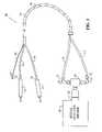
- balanced probe pair assembly 10includes probes 12 , coaxial cables 14 , and may include ground lead 16 . Assembly 10 may be coupled to input channel connector 22 of signal analysis device 18 using, for example, combiner 20 .
- each probe 12includes probe body 24 , probe end 25 , body sleeve 13 , and base connector 15 .
- each probe end 25includes a probe tip sleeve 26 , a coupling probe end connector 50 and a probe tip 27 .
- Probe tip 27includes an elongate tip 28 , a threaded sleeve 29 , a distal tip thread 30 , and a proximate tip thread 31 .
- Threaded sleeve 29engages a distal tip thread 30 and proximate tip thread 31 engages a distal sleeve thread 32 of probe tip sleeve 26 .
- Probe tip 27is constructed of a highly conductive material, for example, nickel-plated brass, and probe tip sleeve 26 is constructed of a nonconductive material, for example, ABS plastic.
- Probe tip 27is electrically connected to a center conductor 34 through a wire 36 and a first surface mount resistor 40 , for example, by soldering.
- Wire 36may be, for example, 30 gauge copper wire.
- Probe tip 27 and center conductor 34are generally electrically isolated from an outer conductor shield 38 which circumscribes center conductor 34 ; however, the termination resistive input network is electrically connected between center conductor 34 and outer conductor shield 38 .
- the resistive input networkincludes first surface mount resistor 40 , for example a 475 ohm surface mount resistor, which is electrically coupled in series between conductive probe tip 27 and center conductor 34 of probe end connector 50 . Additionally, one or more SMD resistors may be electrically connected between center conductor 34 and outer conductive shield 38 of probe end connector 50 . For example, two 100 ohm resistors, first and second surface mount resistors 42 and 44 , may be electrically coupled in parallel between center conductor 34 and the outer conductive probe body, which includes outer conductive shield 38 , providing appropriate termination for 50 ohm matched impedance components.
- first and second surface mount resistors 42 and 44provide a probe attenuation factor of approximately 20 ⁇ ; however, other factors may be achieved with values other than 475 ohms. Additionally, other resistor values may be used for first and second surface mount resistors 42 and 44 to provide a matched impedance value other than 50 ohms.
- the electrical connections between surface mount resistors 40 , 42 and 44 and probe tip 27 and conductor 34 and shield 38may be, for example, a soldered connection 41 .
- resistors 40 , 42 and 44may also be glued, for example epoxyed, in place within outer conductor shield 38 of probe end connector 50 .
- resistors 42 and 44may also be canted at an angle between center conductor 34 and shield 38 .
- using surface mount resistors for providing input termination at the distal termination of coaxial shielding in a balanced electrical probe pairminimizes parasitic inductance and capacitance, thereby improving response characteristics over a wide frequency range.
- the exemplary probe end 25includes male BNC connector 58 and oppositely located probe end connector 50 having female SMA adapter 56 forming a portion of outer conductor shield 38 and center conductor 34 .
- Center conductor 34 in the exemplary embodimentis a hollow cylindrical pin.
- Insulator 37may be located between center conductor 34 and outer conductor shield 38 .
- resistors 42 and 44rest against insulator 37 .
- Probe end connector 50may be, for example, Part No. 16N2740, manufactured by SPC Technology of Chicago, Ill.
- Probe tip sleeve 26 and probe tip 27may be, for example, Part No. 35N776, manufactured by SPC Technology, Inc.
- probe tip 27 and probe end connector 50are facilitated by a non-conductive structure, probe tip sleeve 26 .
- Sleeve 26is secured internally at opposite ends with proximate sleeve thread 33 engaging female SMA adaptor 56 and distal sleeve thread 32 engaging proximate tip thread 31 .
- a different or additional fastening structuremay be used, for example, epoxy.
- Wire 36transits the hollow interior of sleeve 26 and couples resistor 40 and probe tip 27 .
- each probe 12may include a plurality of commercially available connectors and adapters that each form a portion of probe body 24 , are impedance matched, and conduct and shield the electrical signal received at elongate tip 28 .
- probe body 24may include coaxial BNC type connectors 50 , 52 and 54 for coupling probe end 25 with base connector 15 .
- Connectors 50 , 52 and 54may be constructed primarily of a conductive material such as nickel-plated brass and are impedance matched, for example, 50 ohms.
- BNC connector 52may include female BNC adapter 60 and 62 at opposite ends, for example, Part No. 20C3275, manufactured by SPC Technology.
- Female adapter 60 of BNC connector 52may be coupled with male adapter 58 of BNC connector 50 .
- BNC connector 54may include male BNC adapters 64 and 66 at opposite ends, for example, Part No. 20C3274, manufactured by SPC Technology.
- Male adapter 64 of BNC connector 54may be coupled with female adapter 62 of BNC connector 52 .
- base connector 15may be, for example, an RF bulkhead adapter, such as Part No. 93F1409, available from Amphenol, of Wallingford, Conn.
- Exemplary base connector 15includes female BNC adapters 68 and 70 at opposite ends.
- Female adapter 68 of base connector 15may be coupled to male adapter 66 of BNC connector 54 .
- types of low cost impedance matched components that minimize parasitic capacitance and inductancemay be substituted for connectors 15 , 50 , 52 , and 54 .
- Probe 12may also include body sleeve 13 , for example, a 3 1 / 4 -inch long and 1 ⁇ 2 ID metal pipe such as copper which, as shown in FIG. 2A , may be securely received over connectors 15 , 50 , 52 and 54 .
- Body sleeve 13provides an outer conductive shield as well as structural rigidity and a smooth cylindrical shape for probe body 24 .
- the increased diameter of probe body 24 formed by sleeve 13minimizes parasitic capacitance introduced by a user's hand holding probe 12 .
- Probe body 24may also be insulated, for example by nonconductive heat shrink or another suitable material or coating.
- coaxial cables 14may be used to couple probes 12 to combiner 20 , or to an input port of measurement device 18 .
- Cables 14may include male BNC adapter 72 for coupling to female BNC adapter 70 of probe 12 and female BNC adapter 73 of combiner 20 or input channel connector 22 .
- other suitable connectorsmay be used at opposite ends. It is very important that probes 12 and cables 14 be virtually the same materials and dimensions in order to provide proper electrical balancing of the electrical characteristics of probe pair assembly 10 . Variations between probes 12 or cables 14 may cause phase errors, signal amplitude errors, and other electrical errors in the measured signal.
- the insulative coating around the outside coaxial sheath of cables 14may be stripped away and the exposed outer shielding conductor can be electrically coupled at adjacent locations, for example, at junctions 75 , periodically along the cable length, for example every 3 inches.
- the central but substantial portion of cables 14may then be insulated with shrink-wrap 74 , or another suitable insulating material, for insulating solder junctions 75 therealong.
- the balanced probe pair assemblymay be coupled to combiner 20 or another suitable input device of signal analysis device 18 . As shown in FIG. 3 , combiner 20 is coupled with input channel connector 22 , thereby providing a differential input of the circuit nodes probed by probes 12 of balanced probe pair assembly 10 . Although ground connector 16 may be included with probe pair assembly 10 , ground connector 16 would generally only be utilized for single probe measurements, very high common-mode voltage measurements, for example, electrostatic discharge testing, or other similarly indicated measurement circumstances.
- FIG. 4Aa typical frequency response for a commercially available balanced probe pair is shown for the purposes of comparison with FIG. 4B , which under the same test conditions and illustrative chart display shows the much flatter response of the lower-cost inventive balanced probe pair assembly 10 .
- the frequency range for FIGS. 4A and 4Bis 10 MHz to 500 MHz and the attenuation setting is 10 dB.
- FIGS. 4C and 4Dalso demonstrate the performance of probe pair assembly 10 .
- FIG. 4Cillustrates 10 MHz to 2 GHz for 30 dB and
- FIG. 4Dillustrates 10 MHz to 3 GHz for 30 dB.
- FIGS. 4B–4Dillustrate that probe pair assembly 10 has a flatter response characteristic up to at least 1.5 GHz than prior art probes.
Landscapes
- Physics & Mathematics (AREA)
- General Physics & Mathematics (AREA)
- Measuring Leads Or Probes (AREA)
Abstract
Description
Claims (19)
Priority Applications (1)
| Application Number | Priority Date | Filing Date | Title |
|---|---|---|---|
| US10/843,775US7015709B2 (en) | 2004-05-12 | 2004-05-12 | Ultra-broadband differential voltage probes |
Applications Claiming Priority (1)
| Application Number | Priority Date | Filing Date | Title |
|---|---|---|---|
| US10/843,775US7015709B2 (en) | 2004-05-12 | 2004-05-12 | Ultra-broadband differential voltage probes |
Publications (2)
| Publication Number | Publication Date |
|---|---|
| US20050253603A1 US20050253603A1 (en) | 2005-11-17 |
| US7015709B2true US7015709B2 (en) | 2006-03-21 |
Family
ID=35308825
Family Applications (1)
| Application Number | Title | Priority Date | Filing Date |
|---|---|---|---|
| US10/843,775Expired - LifetimeUS7015709B2 (en) | 2004-05-12 | 2004-05-12 | Ultra-broadband differential voltage probes |
Country Status (1)
| Country | Link |
|---|---|
| US (1) | US7015709B2 (en) |
Cited By (61)
| Publication number | Priority date | Publication date | Assignee | Title |
|---|---|---|---|---|
| US20040093716A1 (en)* | 1998-07-14 | 2004-05-20 | Reed Gleason | Membrane probing system |
| US20050122125A1 (en)* | 2002-12-13 | 2005-06-09 | Cascade Microtech, Inc. | Guarded tub enclosure |
| US20050194983A1 (en)* | 1992-06-11 | 2005-09-08 | Schwindt Randy J. | Wafer probe station having a skirting component |
| US20050265667A1 (en)* | 2004-05-28 | 2005-12-01 | Auld Michael D | Adapter for coupling an external post connector or a BNC connector to an SMA bushing |
| US20060164112A1 (en)* | 1997-06-10 | 2006-07-27 | Cascade Microtech, Inc. | Low-current pogo probe card |
| US20060170439A1 (en)* | 2003-05-23 | 2006-08-03 | Cascade Microtech, Inc. | Probe for testing a device under test |
| US20060202708A1 (en)* | 1995-12-01 | 2006-09-14 | Cascade Microtech, Inc. | Low-current probe card |
| US20060208748A1 (en)* | 1997-05-28 | 2006-09-21 | Cascade Microtech, Inc. | Probe holder for testing of a test device |
| US20060214676A1 (en)* | 1996-08-08 | 2006-09-28 | Cascade Microtech, Inc. | Membrane probing system with local contact scrub |
| US20060214677A1 (en)* | 2002-11-13 | 2006-09-28 | Cascade Microtech, Inc. | Probe for combined signals |
| US20060229279A1 (en)* | 2002-03-07 | 2006-10-12 | Hartell Mark G | Artemisinins with improved stability and bioavailability for therapeutic drug development and application |
| US20060267610A1 (en)* | 1997-06-06 | 2006-11-30 | Peters Ron A | Probe station having multiple enclosures |
| US20060284630A1 (en)* | 2000-02-25 | 2006-12-21 | Cascade Microtech, Inc. | Membrane probing system |
| US7176705B2 (en) | 2004-06-07 | 2007-02-13 | Cascade Microtech, Inc. | Thermal optical chuck |
| US7178236B2 (en) | 1999-06-04 | 2007-02-20 | Cascade Microtech, Inc. | Method for constructing a membrane probe using a depression |
| US7187188B2 (en) | 2003-12-24 | 2007-03-06 | Cascade Microtech, Inc. | Chuck with integrated wafer support |
| US7221172B2 (en) | 2003-05-06 | 2007-05-22 | Cascade Microtech, Inc. | Switched suspended conductor and connection |
| US7250626B2 (en) | 2003-10-22 | 2007-07-31 | Cascade Microtech, Inc. | Probe testing structure |
| US7250779B2 (en) | 2002-11-25 | 2007-07-31 | Cascade Microtech, Inc. | Probe station with low inductance path |
| US7268533B2 (en) | 2001-08-31 | 2007-09-11 | Cascade Microtech, Inc. | Optical testing device |
| US20070241740A1 (en)* | 2004-06-19 | 2007-10-18 | United Kingdom Atomic Energy Authority | Hand-Held Probe |
| US7292057B2 (en) | 1999-06-30 | 2007-11-06 | Cascade Microtech, Inc. | Probe station thermal chuck with shielding for capacitive current |
| US7295025B2 (en) | 2002-11-08 | 2007-11-13 | Cascade Microtech, Inc. | Probe station with low noise characteristics |
| US20070294047A1 (en)* | 2005-06-11 | 2007-12-20 | Leonard Hayden | Calibration system |
| US7321233B2 (en) | 1995-04-14 | 2008-01-22 | Cascade Microtech, Inc. | System for evaluating probing networks |
| US7330041B2 (en) | 2004-06-14 | 2008-02-12 | Cascade Microtech, Inc. | Localizing a temperature of a device for testing |
| US7348787B2 (en) | 1992-06-11 | 2008-03-25 | Cascade Microtech, Inc. | Wafer probe station having environment control enclosure |
| US7352168B2 (en) | 2000-09-05 | 2008-04-01 | Cascade Microtech, Inc. | Chuck for holding a device under test |
| US7355420B2 (en) | 2001-08-21 | 2008-04-08 | Cascade Microtech, Inc. | Membrane probing system |
| US7368927B2 (en) | 2004-07-07 | 2008-05-06 | Cascade Microtech, Inc. | Probe head having a membrane suspended probe |
| US7368925B2 (en) | 2002-01-25 | 2008-05-06 | Cascade Microtech, Inc. | Probe station with two platens |
| US7403028B2 (en) | 2006-06-12 | 2008-07-22 | Cascade Microtech, Inc. | Test structure and probe for differential signals |
| US7420381B2 (en) | 2004-09-13 | 2008-09-02 | Cascade Microtech, Inc. | Double sided probing structures |
| US7427868B2 (en) | 2003-12-24 | 2008-09-23 | Cascade Microtech, Inc. | Active wafer probe |
| US7436194B2 (en) | 2002-05-23 | 2008-10-14 | Cascade Microtech, Inc. | Shielded probe with low contact resistance for testing a device under test |
| US7443186B2 (en) | 2006-06-12 | 2008-10-28 | Cascade Microtech, Inc. | On-wafer test structures for differential signals |
| US7449899B2 (en) | 2005-06-08 | 2008-11-11 | Cascade Microtech, Inc. | Probe for high frequency signals |
| US20080281211A1 (en)* | 2003-07-14 | 2008-11-13 | Welch Allyn, Inc. | Motion Management In A Fast Blood Pressure Measurement Device |
| US20080284456A1 (en)* | 2007-05-16 | 2008-11-20 | Pang Sung Man | Test Apparatus of Semiconductor Devices |
| US7456646B2 (en) | 2000-12-04 | 2008-11-25 | Cascade Microtech, Inc. | Wafer probe |
| US7492172B2 (en) | 2003-05-23 | 2009-02-17 | Cascade Microtech, Inc. | Chuck for holding a device under test |
| JP2009034511A (en)* | 2007-07-30 | 2009-02-19 | Dorc Dutch Ophthalmic Research Center (Internatl) Bv | Eye surgical device and eye surgical instrument |
| US20090072846A1 (en)* | 2007-09-14 | 2009-03-19 | Mayo Foundation For Medical Education And Research | High frequency differential test probe for automated printed wiring board test systems |
| US7535247B2 (en) | 2005-01-31 | 2009-05-19 | Cascade Microtech, Inc. | Interface for testing semiconductors |
| US7554322B2 (en) | 2000-09-05 | 2009-06-30 | Cascade Microtech, Inc. | Probe station |
| US7609077B2 (en) | 2006-06-09 | 2009-10-27 | Cascade Microtech, Inc. | Differential signal probe with integral balun |
| US7619419B2 (en) | 2005-06-13 | 2009-11-17 | Cascade Microtech, Inc. | Wideband active-passive differential signal probe |
| US7656172B2 (en) | 2005-01-31 | 2010-02-02 | Cascade Microtech, Inc. | System for testing semiconductors |
| US7723999B2 (en) | 2006-06-12 | 2010-05-25 | Cascade Microtech, Inc. | Calibration structures for differential signal probing |
| US20100148759A1 (en)* | 2008-12-11 | 2010-06-17 | Fluke Corporation | Method and apparatus for indexing an adjustable test probe tip |
| US20100176828A1 (en)* | 2009-01-09 | 2010-07-15 | Fluke Corporation | Reversible test probe and test probe tip |
| US20100182027A1 (en)* | 2009-01-22 | 2010-07-22 | Fluke Corporation | Test lead probe with retractable insulative sleeve |
| US7764072B2 (en) | 2006-06-12 | 2010-07-27 | Cascade Microtech, Inc. | Differential signal probing system |
| US20100255688A1 (en)* | 2006-01-17 | 2010-10-07 | Laird Technologies Gmbh | Rf connector mounting means |
| US7876114B2 (en) | 2007-08-08 | 2011-01-25 | Cascade Microtech, Inc. | Differential waveguide probe |
| US7888957B2 (en) | 2008-10-06 | 2011-02-15 | Cascade Microtech, Inc. | Probing apparatus with impedance optimized interface |
| US8319503B2 (en) | 2008-11-24 | 2012-11-27 | Cascade Microtech, Inc. | Test apparatus for measuring a characteristic of a device under test |
| US8410806B2 (en) | 2008-11-21 | 2013-04-02 | Cascade Microtech, Inc. | Replaceable coupon for a probing apparatus |
| US8446165B2 (en) | 2007-09-14 | 2013-05-21 | Mayo Foundation For Medical Education And Research | Link analysis compliance and calibration verification for automated printed wiring board test systems |
| US20150268272A1 (en)* | 2014-03-18 | 2015-09-24 | National Applied Research Laboratories | Conducted type current probe |
| US11035881B2 (en)* | 2017-04-21 | 2021-06-15 | Rohde & Schwarz Gmbh & Co. Kg | Probe, measuring system as well as test setup |
Families Citing this family (7)
| Publication number | Priority date | Publication date | Assignee | Title |
|---|---|---|---|---|
| DE102005005751B4 (en)* | 2005-02-07 | 2013-08-22 | Infineon Technologies Ag | Test device with reflection-poor signal distribution |
| US8410804B1 (en)* | 2009-02-24 | 2013-04-02 | Keithley Instruments, Inc. | Measurement system with high frequency ground switch |
| DE102010033991A1 (en)* | 2010-03-11 | 2011-12-01 | Rhode & Schwarz Gmbh & Co. Kg | Measuring tip with integrated transducer |
| DE202010013616U1 (en)* | 2010-09-27 | 2010-12-30 | Ingun Prüfmittelbau Gmbh | High-frequency test probe |
| US10386585B2 (en)* | 2016-05-20 | 2019-08-20 | Multilink Inc. | Attachment apparatus for field installable cable termination systems and method |
| US10670626B2 (en)* | 2017-12-15 | 2020-06-02 | Keysight Technologies, Inc. | Test fixture for observing current flow through a set of resistors |
| US12092657B2 (en)* | 2020-02-26 | 2024-09-17 | Raytheon Company | Test probe adapter |
Citations (10)
| Publication number | Priority date | Publication date | Assignee | Title |
|---|---|---|---|---|
| US4978907A (en) | 1989-05-10 | 1990-12-18 | At&T Bell Laboratories | Apparatus and method for expanding the frequency range over which electrical signal amplitudes can be accurately measured |
| US5172051A (en) | 1991-04-24 | 1992-12-15 | Hewlett-Packard Company | Wide bandwidth passive probe |
| US6037787A (en)* | 1998-03-24 | 2000-03-14 | Teradyne, Inc. | High performance probe interface for automatic test equipment |
| US6362635B2 (en)* | 1999-04-08 | 2002-03-26 | Agilent Technologies, Inc. | Split resistor probe and method |
| US6362614B2 (en)* | 1998-10-30 | 2002-03-26 | Agilent Technologies, Inc. | Electronic probe for measuring high impedance tri-state logic circuits |
| US6373348B1 (en) | 2000-08-11 | 2002-04-16 | Tektronix, Inc. | High speed differential attenuator using a low temperature co-fired ceramic substrate |
| US6384614B1 (en)* | 2000-02-05 | 2002-05-07 | Fluke Corporation | Single tip Kelvin probe |
| US6407562B1 (en) | 1999-07-29 | 2002-06-18 | Agilent Technologies, Inc. | Probe tip terminating device providing an easily changeable feed-through termination |
| US20020121907A1 (en) | 2000-11-23 | 2002-09-05 | Karl Griessbaum | Combination of a feedthrough element for an electric high-frequency signal and a probe, and a level meter metering device including a combination of this type |
| US20040085057A1 (en)* | 2002-10-31 | 2004-05-06 | Mctigue Michael Thomas | Voltage probe |
Family Cites Families (1)
| Publication number | Priority date | Publication date | Assignee | Title |
|---|---|---|---|---|
| US121907A (en)* | 1871-12-12 | Improvement in loom shuttle-box mechanisms |
- 2004
- 2004-05-12USUS10/843,775patent/US7015709B2/ennot_activeExpired - Lifetime
Patent Citations (10)
| Publication number | Priority date | Publication date | Assignee | Title |
|---|---|---|---|---|
| US4978907A (en) | 1989-05-10 | 1990-12-18 | At&T Bell Laboratories | Apparatus and method for expanding the frequency range over which electrical signal amplitudes can be accurately measured |
| US5172051A (en) | 1991-04-24 | 1992-12-15 | Hewlett-Packard Company | Wide bandwidth passive probe |
| US6037787A (en)* | 1998-03-24 | 2000-03-14 | Teradyne, Inc. | High performance probe interface for automatic test equipment |
| US6362614B2 (en)* | 1998-10-30 | 2002-03-26 | Agilent Technologies, Inc. | Electronic probe for measuring high impedance tri-state logic circuits |
| US6362635B2 (en)* | 1999-04-08 | 2002-03-26 | Agilent Technologies, Inc. | Split resistor probe and method |
| US6407562B1 (en) | 1999-07-29 | 2002-06-18 | Agilent Technologies, Inc. | Probe tip terminating device providing an easily changeable feed-through termination |
| US6384614B1 (en)* | 2000-02-05 | 2002-05-07 | Fluke Corporation | Single tip Kelvin probe |
| US6373348B1 (en) | 2000-08-11 | 2002-04-16 | Tektronix, Inc. | High speed differential attenuator using a low temperature co-fired ceramic substrate |
| US20020121907A1 (en) | 2000-11-23 | 2002-09-05 | Karl Griessbaum | Combination of a feedthrough element for an electric high-frequency signal and a probe, and a level meter metering device including a combination of this type |
| US20040085057A1 (en)* | 2002-10-31 | 2004-05-06 | Mctigue Michael Thomas | Voltage probe |
Non-Patent Citations (3)
| Title |
|---|
| Fischer Custom Communications, Inc.; High Performance Differential Voltage Probe. Retrieved from www.fischercc.com. |
| Sekel, Steve, Differential Oscilloscope Measurements A Primer on Differential Measurements, Types of Amplifiers, Applications, and Avoiding Common Errors, Tektronix, In., 1996, pp. 1-16, Textronix Publications, USA. |
| Smith, Douglas C., Balanced Prode Extends High-Frequency Measurements, IEEE Circuites & Devices, The Magazine of Electronic and Photonic Systems, Nov. 1994, pp. 19-21, vol. 10, No. 6, Institute of Electrical and Electronics Engineers, Los Gatos, CA, USA. |
Cited By (134)
| Publication number | Priority date | Publication date | Assignee | Title |
|---|---|---|---|---|
| US7492147B2 (en) | 1992-06-11 | 2009-02-17 | Cascade Microtech, Inc. | Wafer probe station having a skirting component |
| US20050194983A1 (en)* | 1992-06-11 | 2005-09-08 | Schwindt Randy J. | Wafer probe station having a skirting component |
| US7330023B2 (en) | 1992-06-11 | 2008-02-12 | Cascade Microtech, Inc. | Wafer probe station having a skirting component |
| US7348787B2 (en) | 1992-06-11 | 2008-03-25 | Cascade Microtech, Inc. | Wafer probe station having environment control enclosure |
| US7595632B2 (en) | 1992-06-11 | 2009-09-29 | Cascade Microtech, Inc. | Wafer probe station having environment control enclosure |
| US7589518B2 (en) | 1992-06-11 | 2009-09-15 | Cascade Microtech, Inc. | Wafer probe station having a skirting component |
| US7321233B2 (en) | 1995-04-14 | 2008-01-22 | Cascade Microtech, Inc. | System for evaluating probing networks |
| US20060202708A1 (en)* | 1995-12-01 | 2006-09-14 | Cascade Microtech, Inc. | Low-current probe card |
| US7541821B2 (en) | 1996-08-08 | 2009-06-02 | Cascade Microtech, Inc. | Membrane probing system with local contact scrub |
| US7893704B2 (en) | 1996-08-08 | 2011-02-22 | Cascade Microtech, Inc. | Membrane probing structure with laterally scrubbing contacts |
| US20060214676A1 (en)* | 1996-08-08 | 2006-09-28 | Cascade Microtech, Inc. | Membrane probing system with local contact scrub |
| US20070296431A1 (en)* | 1996-08-08 | 2007-12-27 | Cascade Microtech, Inc. | Membrane probing system with local contact scrub |
| US7550983B2 (en) | 1996-08-08 | 2009-06-23 | Cascade Microtech, Inc. | Membrane probing system with local contact scrub |
| US20060208748A1 (en)* | 1997-05-28 | 2006-09-21 | Cascade Microtech, Inc. | Probe holder for testing of a test device |
| US7504842B2 (en) | 1997-05-28 | 2009-03-17 | Cascade Microtech, Inc. | Probe holder for testing of a test device |
| US7221174B2 (en) | 1997-05-28 | 2007-05-22 | Cascade Microtech, Inc. | Probe holder for testing of a test device |
| US7250752B2 (en) | 1997-06-06 | 2007-07-31 | Cascade Microtech, Inc. | Probe station having multiple enclosures |
| US7626379B2 (en) | 1997-06-06 | 2009-12-01 | Cascade Microtech, Inc. | Probe station having multiple enclosures |
| US20060267610A1 (en)* | 1997-06-06 | 2006-11-30 | Peters Ron A | Probe station having multiple enclosures |
| US7436170B2 (en) | 1997-06-06 | 2008-10-14 | Cascade Microtech, Inc. | Probe station having multiple enclosures |
| US20060164112A1 (en)* | 1997-06-10 | 2006-07-27 | Cascade Microtech, Inc. | Low-current pogo probe card |
| US8451017B2 (en) | 1998-07-14 | 2013-05-28 | Cascade Microtech, Inc. | Membrane probing method using improved contact |
| US7400155B2 (en) | 1998-07-14 | 2008-07-15 | Cascade Microtech, Inc. | Membrane probing system |
| US7681312B2 (en) | 1998-07-14 | 2010-03-23 | Cascade Microtech, Inc. | Membrane probing system |
| US7761986B2 (en) | 1998-07-14 | 2010-07-27 | Cascade Microtech, Inc. | Membrane probing method using improved contact |
| US20040093716A1 (en)* | 1998-07-14 | 2004-05-20 | Reed Gleason | Membrane probing system |
| US7266889B2 (en) | 1998-07-14 | 2007-09-11 | Cascade Microtech, Inc. | Membrane probing system |
| US7178236B2 (en) | 1999-06-04 | 2007-02-20 | Cascade Microtech, Inc. | Method for constructing a membrane probe using a depression |
| US20070074392A1 (en)* | 1999-06-04 | 2007-04-05 | Cascade Microtech, Inc. | Membrane probing system |
| US7533462B2 (en) | 1999-06-04 | 2009-05-19 | Cascade Microtech, Inc. | Method of constructing a membrane probe |
| US7616017B2 (en) | 1999-06-30 | 2009-11-10 | Cascade Microtech, Inc. | Probe station thermal chuck with shielding for capacitive current |
| US7292057B2 (en) | 1999-06-30 | 2007-11-06 | Cascade Microtech, Inc. | Probe station thermal chuck with shielding for capacitive current |
| US7403025B2 (en) | 2000-02-25 | 2008-07-22 | Cascade Microtech, Inc. | Membrane probing system |
| US20060284630A1 (en)* | 2000-02-25 | 2006-12-21 | Cascade Microtech, Inc. | Membrane probing system |
| US7423419B2 (en) | 2000-09-05 | 2008-09-09 | Cascade Microtech, Inc. | Chuck for holding a device under test |
| US7514915B2 (en) | 2000-09-05 | 2009-04-07 | Cascade Microtech, Inc. | Chuck for holding a device under test |
| US7688062B2 (en) | 2000-09-05 | 2010-03-30 | Cascade Microtech, Inc. | Probe station |
| US7352168B2 (en) | 2000-09-05 | 2008-04-01 | Cascade Microtech, Inc. | Chuck for holding a device under test |
| US7518358B2 (en) | 2000-09-05 | 2009-04-14 | Cascade Microtech, Inc. | Chuck for holding a device under test |
| US7969173B2 (en) | 2000-09-05 | 2011-06-28 | Cascade Microtech, Inc. | Chuck for holding a device under test |
| US7554322B2 (en) | 2000-09-05 | 2009-06-30 | Cascade Microtech, Inc. | Probe station |
| US7501810B2 (en) | 2000-09-05 | 2009-03-10 | Cascade Microtech, Inc. | Chuck for holding a device under test |
| US7456646B2 (en) | 2000-12-04 | 2008-11-25 | Cascade Microtech, Inc. | Wafer probe |
| US7495461B2 (en) | 2000-12-04 | 2009-02-24 | Cascade Microtech, Inc. | Wafer probe |
| US7761983B2 (en) | 2000-12-04 | 2010-07-27 | Cascade Microtech, Inc. | Method of assembling a wafer probe |
| US7688097B2 (en) | 2000-12-04 | 2010-03-30 | Cascade Microtech, Inc. | Wafer probe |
| US20080111571A1 (en)* | 2001-08-21 | 2008-05-15 | Cascade Microtech, Inc. | Membrane probing system |
| US7492175B2 (en) | 2001-08-21 | 2009-02-17 | Cascade Microtech, Inc. | Membrane probing system |
| US7355420B2 (en) | 2001-08-21 | 2008-04-08 | Cascade Microtech, Inc. | Membrane probing system |
| US7268533B2 (en) | 2001-08-31 | 2007-09-11 | Cascade Microtech, Inc. | Optical testing device |
| US7368925B2 (en) | 2002-01-25 | 2008-05-06 | Cascade Microtech, Inc. | Probe station with two platens |
| US20060229279A1 (en)* | 2002-03-07 | 2006-10-12 | Hartell Mark G | Artemisinins with improved stability and bioavailability for therapeutic drug development and application |
| US7518387B2 (en) | 2002-05-23 | 2009-04-14 | Cascade Microtech, Inc. | Shielded probe for testing a device under test |
| US7436194B2 (en) | 2002-05-23 | 2008-10-14 | Cascade Microtech, Inc. | Shielded probe with low contact resistance for testing a device under test |
| US7489149B2 (en) | 2002-05-23 | 2009-02-10 | Cascade Microtech, Inc. | Shielded probe for testing a device under test |
| US7482823B2 (en) | 2002-05-23 | 2009-01-27 | Cascade Microtech, Inc. | Shielded probe for testing a device under test |
| US7295025B2 (en) | 2002-11-08 | 2007-11-13 | Cascade Microtech, Inc. | Probe station with low noise characteristics |
| US7550984B2 (en) | 2002-11-08 | 2009-06-23 | Cascade Microtech, Inc. | Probe station with low noise characteristics |
| US7417446B2 (en) | 2002-11-13 | 2008-08-26 | Cascade Microtech, Inc. | Probe for combined signals |
| US7453276B2 (en) | 2002-11-13 | 2008-11-18 | Cascade Microtech, Inc. | Probe for combined signals |
| US7205784B2 (en) | 2002-11-13 | 2007-04-17 | Cascade Microtech, Inc. | Probe for combined signals |
| US20060214677A1 (en)* | 2002-11-13 | 2006-09-28 | Cascade Microtech, Inc. | Probe for combined signals |
| US7285969B2 (en) | 2002-11-13 | 2007-10-23 | Cascade Microtech, Inc. | Probe for combined signals |
| US7498828B2 (en) | 2002-11-25 | 2009-03-03 | Cascade Microtech, Inc. | Probe station with low inductance path |
| US7250779B2 (en) | 2002-11-25 | 2007-07-31 | Cascade Microtech, Inc. | Probe station with low inductance path |
| US7221146B2 (en) | 2002-12-13 | 2007-05-22 | Cascade Microtech, Inc. | Guarded tub enclosure |
| US20050122125A1 (en)* | 2002-12-13 | 2005-06-09 | Cascade Microtech, Inc. | Guarded tub enclosure |
| US7639003B2 (en) | 2002-12-13 | 2009-12-29 | Cascade Microtech, Inc. | Guarded tub enclosure |
| US7468609B2 (en) | 2003-05-06 | 2008-12-23 | Cascade Microtech, Inc. | Switched suspended conductor and connection |
| US7221172B2 (en) | 2003-05-06 | 2007-05-22 | Cascade Microtech, Inc. | Switched suspended conductor and connection |
| US7492172B2 (en) | 2003-05-23 | 2009-02-17 | Cascade Microtech, Inc. | Chuck for holding a device under test |
| US20060170439A1 (en)* | 2003-05-23 | 2006-08-03 | Cascade Microtech, Inc. | Probe for testing a device under test |
| US7498829B2 (en) | 2003-05-23 | 2009-03-03 | Cascade Microtech, Inc. | Shielded probe for testing a device under test |
| US7271603B2 (en) | 2003-05-23 | 2007-09-18 | Cascade Microtech, Inc. | Shielded probe for testing a device under test |
| US7898273B2 (en) | 2003-05-23 | 2011-03-01 | Cascade Microtech, Inc. | Probe for testing a device under test |
| US7501842B2 (en) | 2003-05-23 | 2009-03-10 | Cascade Microtech, Inc. | Shielded probe for testing a device under test |
| US7876115B2 (en) | 2003-05-23 | 2011-01-25 | Cascade Microtech, Inc. | Chuck for holding a device under test |
| US8734355B2 (en) | 2003-07-14 | 2014-05-27 | Welch Allyn, Inc. | Motion management in a fast blood pressure measurement device |
| US20080281211A1 (en)* | 2003-07-14 | 2008-11-13 | Welch Allyn, Inc. | Motion Management In A Fast Blood Pressure Measurement Device |
| US7250626B2 (en) | 2003-10-22 | 2007-07-31 | Cascade Microtech, Inc. | Probe testing structure |
| US8069491B2 (en) | 2003-10-22 | 2011-11-29 | Cascade Microtech, Inc. | Probe testing structure |
| US7759953B2 (en) | 2003-12-24 | 2010-07-20 | Cascade Microtech, Inc. | Active wafer probe |
| US7688091B2 (en) | 2003-12-24 | 2010-03-30 | Cascade Microtech, Inc. | Chuck with integrated wafer support |
| US7362115B2 (en) | 2003-12-24 | 2008-04-22 | Cascade Microtech, Inc. | Chuck with integrated wafer support |
| US7187188B2 (en) | 2003-12-24 | 2007-03-06 | Cascade Microtech, Inc. | Chuck with integrated wafer support |
| US7427868B2 (en) | 2003-12-24 | 2008-09-23 | Cascade Microtech, Inc. | Active wafer probe |
| US7275873B2 (en)* | 2004-05-28 | 2007-10-02 | Synergetics, Inc. | Adapter for coupling an external post connector or a BNC connector to an SMA bushing |
| US20050265667A1 (en)* | 2004-05-28 | 2005-12-01 | Auld Michael D | Adapter for coupling an external post connector or a BNC connector to an SMA bushing |
| WO2005119319A3 (en)* | 2004-05-28 | 2006-09-14 | Synergetics Inc | Adapter for coupling an external post connector or a bnc connector to an sma bushing |
| US7504823B2 (en) | 2004-06-07 | 2009-03-17 | Cascade Microtech, Inc. | Thermal optical chuck |
| US7176705B2 (en) | 2004-06-07 | 2007-02-13 | Cascade Microtech, Inc. | Thermal optical chuck |
| US7330041B2 (en) | 2004-06-14 | 2008-02-12 | Cascade Microtech, Inc. | Localizing a temperature of a device for testing |
| US20070241740A1 (en)* | 2004-06-19 | 2007-10-18 | United Kingdom Atomic Energy Authority | Hand-Held Probe |
| US7514944B2 (en) | 2004-07-07 | 2009-04-07 | Cascade Microtech, Inc. | Probe head having a membrane suspended probe |
| US7368927B2 (en) | 2004-07-07 | 2008-05-06 | Cascade Microtech, Inc. | Probe head having a membrane suspended probe |
| US8013623B2 (en) | 2004-09-13 | 2011-09-06 | Cascade Microtech, Inc. | Double sided probing structures |
| US7420381B2 (en) | 2004-09-13 | 2008-09-02 | Cascade Microtech, Inc. | Double sided probing structures |
| US7535247B2 (en) | 2005-01-31 | 2009-05-19 | Cascade Microtech, Inc. | Interface for testing semiconductors |
| US7656172B2 (en) | 2005-01-31 | 2010-02-02 | Cascade Microtech, Inc. | System for testing semiconductors |
| US7898281B2 (en) | 2005-01-31 | 2011-03-01 | Cascade Mircotech, Inc. | Interface for testing semiconductors |
| US7940069B2 (en) | 2005-01-31 | 2011-05-10 | Cascade Microtech, Inc. | System for testing semiconductors |
| US7449899B2 (en) | 2005-06-08 | 2008-11-11 | Cascade Microtech, Inc. | Probe for high frequency signals |
| US20070294047A1 (en)* | 2005-06-11 | 2007-12-20 | Leonard Hayden | Calibration system |
| US7619419B2 (en) | 2005-06-13 | 2009-11-17 | Cascade Microtech, Inc. | Wideband active-passive differential signal probe |
| US7909612B2 (en)* | 2006-01-17 | 2011-03-22 | Laird Technologies, Inc. | RF connector mounting means |
| US20100255688A1 (en)* | 2006-01-17 | 2010-10-07 | Laird Technologies Gmbh | Rf connector mounting means |
| US7609077B2 (en) | 2006-06-09 | 2009-10-27 | Cascade Microtech, Inc. | Differential signal probe with integral balun |
| US7443186B2 (en) | 2006-06-12 | 2008-10-28 | Cascade Microtech, Inc. | On-wafer test structures for differential signals |
| US7723999B2 (en) | 2006-06-12 | 2010-05-25 | Cascade Microtech, Inc. | Calibration structures for differential signal probing |
| US7403028B2 (en) | 2006-06-12 | 2008-07-22 | Cascade Microtech, Inc. | Test structure and probe for differential signals |
| US7764072B2 (en) | 2006-06-12 | 2010-07-27 | Cascade Microtech, Inc. | Differential signal probing system |
| US7750652B2 (en) | 2006-06-12 | 2010-07-06 | Cascade Microtech, Inc. | Test structure and probe for differential signals |
| US20080284456A1 (en)* | 2007-05-16 | 2008-11-20 | Pang Sung Man | Test Apparatus of Semiconductor Devices |
| JP2009034511A (en)* | 2007-07-30 | 2009-02-19 | Dorc Dutch Ophthalmic Research Center (Internatl) Bv | Eye surgical device and eye surgical instrument |
| US7876114B2 (en) | 2007-08-08 | 2011-01-25 | Cascade Microtech, Inc. | Differential waveguide probe |
| US7906979B2 (en)* | 2007-09-14 | 2011-03-15 | Mayo Foundation For Medical Education And Research | High frequency differential test probe for automated printed wiring board test systems |
| US20090072846A1 (en)* | 2007-09-14 | 2009-03-19 | Mayo Foundation For Medical Education And Research | High frequency differential test probe for automated printed wiring board test systems |
| US8446165B2 (en) | 2007-09-14 | 2013-05-21 | Mayo Foundation For Medical Education And Research | Link analysis compliance and calibration verification for automated printed wiring board test systems |
| US7888957B2 (en) | 2008-10-06 | 2011-02-15 | Cascade Microtech, Inc. | Probing apparatus with impedance optimized interface |
| US10267848B2 (en) | 2008-11-21 | 2019-04-23 | Formfactor Beaverton, Inc. | Method of electrically contacting a bond pad of a device under test with a probe |
| US9429638B2 (en) | 2008-11-21 | 2016-08-30 | Cascade Microtech, Inc. | Method of replacing an existing contact of a wafer probing assembly |
| US8410806B2 (en) | 2008-11-21 | 2013-04-02 | Cascade Microtech, Inc. | Replaceable coupon for a probing apparatus |
| US8319503B2 (en) | 2008-11-24 | 2012-11-27 | Cascade Microtech, Inc. | Test apparatus for measuring a characteristic of a device under test |
| US8922231B2 (en)* | 2008-12-11 | 2014-12-30 | Fluke Corporation | Method and apparatus for indexing an adjustable test probe tip |
| US20120119771A1 (en)* | 2008-12-11 | 2012-05-17 | Fluke Corporation | Method and apparatus for indexing an adjustable test probe tip |
| US8154316B2 (en)* | 2008-12-11 | 2012-04-10 | Fluke Corporation | Method and apparatus for indexing an adjustable test probe tip |
| US20100148759A1 (en)* | 2008-12-11 | 2010-06-17 | Fluke Corporation | Method and apparatus for indexing an adjustable test probe tip |
| US7902848B2 (en)* | 2009-01-09 | 2011-03-08 | Fluke Corporation | Reversible test probe and test probe tip |
| US20100176828A1 (en)* | 2009-01-09 | 2010-07-15 | Fluke Corporation | Reversible test probe and test probe tip |
| US20100182027A1 (en)* | 2009-01-22 | 2010-07-22 | Fluke Corporation | Test lead probe with retractable insulative sleeve |
| US7880487B2 (en) | 2009-01-22 | 2011-02-01 | Fluke Corporation | Test lead probe with retractable insulative sleeve |
| US9709601B2 (en)* | 2014-03-18 | 2017-07-18 | National Applied Research Laboratories | Conducted type current probe |
| US20150268272A1 (en)* | 2014-03-18 | 2015-09-24 | National Applied Research Laboratories | Conducted type current probe |
| US11035881B2 (en)* | 2017-04-21 | 2021-06-15 | Rohde & Schwarz Gmbh & Co. Kg | Probe, measuring system as well as test setup |
Also Published As
| Publication number | Publication date |
|---|---|
| US20050253603A1 (en) | 2005-11-17 |
Similar Documents
| Publication | Publication Date | Title |
|---|---|---|
| US7015709B2 (en) | Ultra-broadband differential voltage probes | |
| EP0985154B1 (en) | Broadband impedance matching probe | |
| US6784679B2 (en) | Differential coaxial contact array for high-density, high-speed signals | |
| US6724205B1 (en) | Probe for combined signals | |
| US6407562B1 (en) | Probe tip terminating device providing an easily changeable feed-through termination | |
| US20070252606A1 (en) | Shielded Probe Apparatus for Probing Semiconductor Wafer | |
| JPH0682480A (en) | Measuring probe | |
| JPH0835987A (en) | probe | |
| JPH1038914A (en) | Connecting device of apparatus to test lead | |
| JPS6337465B2 (en) | ||
| US20070222468A1 (en) | High bandwidth probe system | |
| US5218293A (en) | Passive high-frequency signal probe | |
| US5463323A (en) | Impedance meter | |
| CN108872644B (en) | Probe end interface with shield | |
| US7482814B2 (en) | Electric/magnetic field sensor | |
| US11035881B2 (en) | Probe, measuring system as well as test setup | |
| WO2021261193A1 (en) | Current measurement component, current measurement device, and current measurement method | |
| CN114384456A (en) | Line impedance stabilization network calibration adapter | |
| US11705611B2 (en) | High-frequency coaxial attenuator | |
| EP0290182A1 (en) | High frequency passive probe | |
| US6753676B1 (en) | RF test probe | |
| Mcdowell et al. | Surface transfer impedance measurements on subminiature coaxial cables | |
| JPH0743657Y2 (en) | Measuring instrument probe | |
| JP2022008080A (en) | Current measuring parts, current measuring devices and current measuring methods | |
| Fowler | CATV cable assemblies: screening requirements and performance |
Legal Events
| Date | Code | Title | Description |
|---|---|---|---|
| AS | Assignment | Owner name:DELPHI TECHNOLOGIES INC., MICHIGAN Free format text:ASSIGNMENT OF ASSIGNORS INTEREST;ASSIGNORS:CAPPS, CHARLES P.;JOHNSON, BRIAN W.;GLOUDEMANS, JEFFREY M.;AND OTHERS;REEL/FRAME:015325/0521;SIGNING DATES FROM 20040505 TO 20040506 | |
| STCF | Information on status: patent grant | Free format text:PATENTED CASE | |
| FPAY | Fee payment | Year of fee payment:4 | |
| FPAY | Fee payment | Year of fee payment:8 | |
| MAFP | Maintenance fee payment | Free format text:PAYMENT OF MAINTENANCE FEE, 12TH YEAR, LARGE ENTITY (ORIGINAL EVENT CODE: M1553) Year of fee payment:12 | |
| AS | Assignment | Owner name:APTIV TECHNOLOGIES LIMITED, BARBADOS Free format text:ASSIGNMENT OF ASSIGNORS INTEREST;ASSIGNOR:DELPHI TECHNOLOGIES INC.;REEL/FRAME:047143/0874 Effective date:20180101 | |
| AS | Assignment | Owner name:APTIV TECHNOLOGIES (2) S.A R.L., LUXEMBOURG Free format text:ENTITY CONVERSION;ASSIGNOR:APTIV TECHNOLOGIES LIMITED;REEL/FRAME:066746/0001 Effective date:20230818 Owner name:APTIV MANUFACTURING MANAGEMENT SERVICES S.A R.L., LUXEMBOURG Free format text:MERGER;ASSIGNOR:APTIV TECHNOLOGIES (2) S.A R.L.;REEL/FRAME:066566/0173 Effective date:20231005 Owner name:APTIV TECHNOLOGIES AG, SWITZERLAND Free format text:ASSIGNMENT OF ASSIGNORS INTEREST;ASSIGNOR:APTIV MANUFACTURING MANAGEMENT SERVICES S.A R.L.;REEL/FRAME:066551/0219 Effective date:20231006 |