US7015640B2 - Diffusion barrier coatings having graded compositions and devices incorporating the same - Google Patents
Diffusion barrier coatings having graded compositions and devices incorporating the sameDownload PDFInfo
- Publication number
- US7015640B2 US7015640B2US10/065,018US6501802AUS7015640B2US 7015640 B2US7015640 B2US 7015640B2US 6501802 AUS6501802 AUS 6501802AUS 7015640 B2US7015640 B2US 7015640B2
- Authority
- US
- United States
- Prior art keywords
- organic
- light
- substrate
- emitting device
- composition
- Prior art date
- Legal status (The legal status is an assumption and is not a legal conclusion. Google has not performed a legal analysis and makes no representation as to the accuracy of the status listed.)
- Expired - Lifetime, expires
Links
- 239000000203mixtureSubstances0.000titleclaimsabstractdescription122
- 238000000576coating methodMethods0.000titleclaimsabstractdescription112
- 230000004888barrier functionEffects0.000titleclaimsabstractdescription52
- 238000009792diffusion processMethods0.000titleabstractdescription15
- 239000000758substrateSubstances0.000claimsabstractdescription153
- 239000000463materialSubstances0.000claimsabstractdescription123
- 239000011248coating agentSubstances0.000claimsabstractdescription111
- -1poly(cyclic olefinsChemical class0.000claimsdescription46
- 238000000034methodMethods0.000claimsdescription31
- 238000000151depositionMethods0.000claimsdescription26
- 229910052751metalInorganic materials0.000claimsdescription24
- 239000002184metalSubstances0.000claimsdescription24
- 239000002245particleSubstances0.000claimsdescription21
- 238000000623plasma-assisted chemical vapour depositionMethods0.000claimsdescription18
- 238000005229chemical vapour depositionMethods0.000claimsdescription14
- 230000005855radiationEffects0.000claimsdescription14
- 238000002347injectionMethods0.000claimsdescription12
- 239000007924injectionSubstances0.000claimsdescription12
- 238000000149argon plasma sinteringMethods0.000claimsdescription10
- 239000003822epoxy resinSubstances0.000claimsdescription10
- LNEPOXFFQSENCJ-UHFFFAOYSA-NhaloperidolChemical compoundC1CC(O)(C=2C=CC(Cl)=CC=2)CCN1CCCC(=O)C1=CC=C(F)C=C1LNEPOXFFQSENCJ-UHFFFAOYSA-N0.000claimsdescription10
- 239000011368organic materialSubstances0.000claimsdescription10
- 229920000647polyepoxidePolymers0.000claimsdescription10
- 229920000548poly(silane) polymerPolymers0.000claimsdescription9
- MWPLVEDNUUSJAV-UHFFFAOYSA-NanthraceneChemical compoundC1=CC=CC2=CC3=CC=CC=C3C=C21MWPLVEDNUUSJAV-UHFFFAOYSA-N0.000claimsdescription8
- VPUGDVKSAQVFFS-UHFFFAOYSA-NcoroneneChemical compoundC1=C(C2=C34)C=CC3=CC=C(C=C3)C4=C4C3=CC=C(C=C3)C4=C2C3=C1VPUGDVKSAQVFFS-UHFFFAOYSA-N0.000claimsdescription8
- UHOVQNZJYSORNB-UHFFFAOYSA-NmonobenzeneNatural productsC1=CC=CC=C1UHOVQNZJYSORNB-UHFFFAOYSA-N0.000claimsdescription8
- 229920000058polyacrylatePolymers0.000claimsdescription8
- 229920001577copolymerPolymers0.000claimsdescription7
- 238000004544sputter depositionMethods0.000claimsdescription7
- 229910010293ceramic materialInorganic materials0.000claimsdescription6
- 230000005525hole transportEffects0.000claimsdescription6
- 229920000515polycarbonatePolymers0.000claimsdescription6
- 239000004417polycarbonateSubstances0.000claimsdescription6
- 229920006393polyether sulfonePolymers0.000claimsdescription6
- 229920000139polyethylene terephthalatePolymers0.000claimsdescription6
- 239000005020polyethylene terephthalateSubstances0.000claimsdescription6
- 229920001296polysiloxanePolymers0.000claimsdescription6
- 229910052712strontiumInorganic materials0.000claimsdescription6
- 229910052688GadoliniumInorganic materials0.000claimsdescription5
- 239000004695Polyether sulfoneSubstances0.000claimsdescription5
- 239000004697PolyetherimideSubstances0.000claimsdescription5
- 239000004642PolyimideSubstances0.000claimsdescription5
- 229910052782aluminiumInorganic materials0.000claimsdescription5
- 238000009616inductively coupled plasmaMethods0.000claimsdescription5
- 239000011777magnesiumSubstances0.000claimsdescription5
- 125000002080perylenyl groupChemical groupC1(=CC=C2C=CC=C3C4=CC=CC5=CC=CC(C1=C23)=C45)*0.000claimsdescription5
- 229920003227poly(N-vinyl carbazole)Polymers0.000claimsdescription5
- 229920000728polyesterPolymers0.000claimsdescription5
- 229920001601polyetherimidePolymers0.000claimsdescription5
- 229920001721polyimidePolymers0.000claimsdescription5
- 238000005546reactive sputteringMethods0.000claimsdescription5
- ZVYYAYJIGYODSD-LNTINUHCSA-K(z)-4-bis[[(z)-4-oxopent-2-en-2-yl]oxy]gallanyloxypent-3-en-2-oneChemical compound[Ga+3].C\C([O-])=C\C(C)=O.C\C([O-])=C\C(C)=O.C\C([O-])=C\C(C)=OZVYYAYJIGYODSD-LNTINUHCSA-K0.000claimsdescription4
- POILWHVDKZOXJZ-ARJAWSKDSA-M(z)-4-oxopent-2-en-2-olateChemical compoundC\C([O-])=C\C(C)=OPOILWHVDKZOXJZ-ARJAWSKDSA-M0.000claimsdescription4
- KLCLIOISYBHYDZ-UHFFFAOYSA-N1,4,4-triphenylbuta-1,3-dienylbenzeneChemical compoundC=1C=CC=CC=1C(C=1C=CC=CC=1)=CC=C(C=1C=CC=CC=1)C1=CC=CC=C1KLCLIOISYBHYDZ-UHFFFAOYSA-N0.000claimsdescription4
- BRSRUYVJULRMRQ-UHFFFAOYSA-N1-phenylanthraceneChemical compoundC1=CC=CC=C1C1=CC=CC2=CC3=CC=CC=C3C=C12BRSRUYVJULRMRQ-UHFFFAOYSA-N0.000claimsdescription4
- GOLORTLGFDVFDW-UHFFFAOYSA-N3-(1h-benzimidazol-2-yl)-7-(diethylamino)chromen-2-oneChemical compoundC1=CC=C2NC(C3=CC4=CC=C(C=C4OC3=O)N(CC)CC)=NC2=C1GOLORTLGFDVFDW-UHFFFAOYSA-N0.000claimsdescription4
- 239000007983Tris bufferSubstances0.000claimsdescription4
- 125000002490anilino groupChemical group[H]N(*)C1=C([H])C([H])=C([H])C([H])=C1[H]0.000claimsdescription4
- 229910052791calciumInorganic materials0.000claimsdescription4
- 238000006243chemical reactionMethods0.000claimsdescription4
- 239000004020conductorSubstances0.000claimsdescription4
- 229910052731fluorineInorganic materials0.000claimsdescription4
- YBMRDBCBODYGJE-UHFFFAOYSA-Ngermanium oxideInorganic materialsO=[Ge]=OYBMRDBCBODYGJE-UHFFFAOYSA-N0.000claimsdescription4
- SKWCWFYBFZIXHE-UHFFFAOYSA-Kindium acetylacetonateChemical compoundCC(=O)C=C(C)O[In](OC(C)=CC(C)=O)OC(C)=CC(C)=OSKWCWFYBFZIXHE-UHFFFAOYSA-K0.000claimsdescription4
- 150000002739metalsChemical class0.000claimsdescription4
- 150000004767nitridesChemical class0.000claimsdescription4
- CSHWQDPOILHKBI-UHFFFAOYSA-NperyreneNatural productsC1=CC(C2=CC=CC=3C2=C2C=CC=3)=C3C2=CC=CC3=C1CSHWQDPOILHKBI-UHFFFAOYSA-N0.000claimsdescription4
- 229910052761rare earth metalInorganic materials0.000claimsdescription4
- YYMBJDOZVAITBP-UHFFFAOYSA-NrubreneChemical compoundC1=CC=CC=C1C(C1=C(C=2C=CC=CC=2)C2=CC=CC=C2C(C=2C=CC=CC=2)=C11)=C(C=CC=C2)C2=C1C1=CC=CC=C1YYMBJDOZVAITBP-UHFFFAOYSA-N0.000claimsdescription4
- 238000001429visible spectrumMethods0.000claimsdescription4
- RUDFQVOCFDJEEF-UHFFFAOYSA-Nyttrium(III) oxideInorganic materials[O-2].[O-2].[O-2].[Y+3].[Y+3]RUDFQVOCFDJEEF-UHFFFAOYSA-N0.000claimsdescription4
- 229910010272inorganic materialInorganic materials0.000claimsdescription3
- 229910052749magnesiumInorganic materials0.000claimsdescription3
- 229910044991metal oxideInorganic materials0.000claimsdescription3
- 150000004706metal oxidesChemical class0.000claimsdescription3
- 150000002910rare earth metalsChemical class0.000claimsdescription3
- 229910052727yttriumInorganic materials0.000claimsdescription3
- 229910052733galliumInorganic materials0.000claimsdescription2
- 229910052909inorganic silicateInorganic materials0.000claimsdescription2
- 150000001247metal acetylidesChemical class0.000claimsdescription2
- XBIUWALDKXACEA-UHFFFAOYSA-N3-[bis(2,4-dioxopentan-3-yl)alumanyl]pentane-2,4-dioneChemical compoundCC(=O)C(C(C)=O)[Al](C(C(C)=O)C(C)=O)C(C(C)=O)C(C)=OXBIUWALDKXACEA-UHFFFAOYSA-N0.000claims3
- 229920000265PolyparaphenylenePolymers0.000claims3
- 239000011159matrix materialSubstances0.000claims3
- 229910052788bariumInorganic materials0.000claims2
- FYYHWMGAXLPEAU-UHFFFAOYSA-NMagnesiumChemical compound[Mg]FYYHWMGAXLPEAU-UHFFFAOYSA-N0.000claims1
- QVGXLLKOCUKJST-UHFFFAOYSA-Natomic oxygenChemical compound[O]QVGXLLKOCUKJST-UHFFFAOYSA-N0.000abstractdescription16
- 229910052760oxygenInorganic materials0.000abstractdescription16
- 239000001301oxygenSubstances0.000abstractdescription16
- 230000005540biological transmissionEffects0.000abstractdescription14
- XLYOFNOQVPJJNP-UHFFFAOYSA-NwaterChemical compoundOXLYOFNOQVPJJNP-UHFFFAOYSA-N0.000abstractdescription13
- 239000013626chemical specieSubstances0.000abstractdescription9
- 239000002131composite materialSubstances0.000abstractdescription6
- 239000010410layerSubstances0.000description93
- 239000010408filmSubstances0.000description25
- 210000002381plasmaAnatomy0.000description21
- 239000007789gasSubstances0.000description17
- 239000000376reactantSubstances0.000description17
- OAICVXFJPJFONN-UHFFFAOYSA-NPhosphorusChemical compound[P]OAICVXFJPJFONN-UHFFFAOYSA-N0.000description15
- 230000008021depositionEffects0.000description12
- 229920000642polymerPolymers0.000description11
- QGZKDVFQNNGYKY-UHFFFAOYSA-NAmmoniaChemical compoundNQGZKDVFQNNGYKY-UHFFFAOYSA-N0.000description10
- BLRPTPMANUNPDV-UHFFFAOYSA-NSilaneChemical compound[SiH4]BLRPTPMANUNPDV-UHFFFAOYSA-N0.000description9
- MCMNRKCIXSYSNV-UHFFFAOYSA-NZirconium dioxideChemical compoundO=[Zr]=OMCMNRKCIXSYSNV-UHFFFAOYSA-N0.000description8
- 238000004519manufacturing processMethods0.000description8
- 229910000077silaneInorganic materials0.000description8
- 230000006870functionEffects0.000description7
- 239000011521glassSubstances0.000description7
- 229910019655synthetic inorganic crystalline materialInorganic materials0.000description7
- 241000894007speciesSpecies0.000description6
- 229910021529ammoniaInorganic materials0.000description5
- 230000008901benefitEffects0.000description5
- 229920003023plasticPolymers0.000description5
- IJGRMHOSHXDMSA-UHFFFAOYSA-NAtomic nitrogenChemical compoundN#NIJGRMHOSHXDMSA-UHFFFAOYSA-N0.000description4
- XUIMIQQOPSSXEZ-UHFFFAOYSA-NSiliconChemical compound[Si]XUIMIQQOPSSXEZ-UHFFFAOYSA-N0.000description4
- XAGFODPZIPBFFR-UHFFFAOYSA-NaluminiumChemical compound[Al]XAGFODPZIPBFFR-UHFFFAOYSA-N0.000description4
- 150000001875compoundsChemical class0.000description4
- 238000010586diagramMethods0.000description4
- LEQAOMBKQFMDFZ-UHFFFAOYSA-NglyoxalChemical compoundO=CC=OLEQAOMBKQFMDFZ-UHFFFAOYSA-N0.000description4
- FFUAGWLWBBFQJT-UHFFFAOYSA-NhexamethyldisilazaneChemical compoundC[Si](C)(C)N[Si](C)(C)CFFUAGWLWBBFQJT-UHFFFAOYSA-N0.000description4
- 150000002500ionsChemical class0.000description4
- VNWKTOKETHGBQD-UHFFFAOYSA-NmethaneChemical compoundCVNWKTOKETHGBQD-UHFFFAOYSA-N0.000description4
- 238000005240physical vapour depositionMethods0.000description4
- 239000004033plasticSubstances0.000description4
- 239000010703siliconSubstances0.000description4
- 229910052710siliconInorganic materials0.000description4
- 229910052684CeriumInorganic materials0.000description3
- GOOHAUXETOMSMM-UHFFFAOYSA-NPropylene oxideChemical compoundCC1CO1GOOHAUXETOMSMM-UHFFFAOYSA-N0.000description3
- 229910045601alloyInorganic materials0.000description3
- 239000000956alloySubstances0.000description3
- 230000015556catabolic processEffects0.000description3
- 239000000919ceramicSubstances0.000description3
- 239000002800charge carrierSubstances0.000description3
- 238000006731degradation reactionMethods0.000description3
- 238000003618dip coatingMethods0.000description3
- 239000012044organic layerSubstances0.000description3
- 239000013047polymeric layerSubstances0.000description3
- 238000005215recombinationMethods0.000description3
- 230000006798recombinationEffects0.000description3
- 229910052709silverInorganic materials0.000description3
- 239000002904solventSubstances0.000description3
- 230000003595spectral effectEffects0.000description3
- 238000005507sprayingMethods0.000description3
- 238000012546transferMethods0.000description3
- 229910019901yttrium aluminum garnetInorganic materials0.000description3
- XKRFYHLGVUSROY-UHFFFAOYSA-NArgonChemical compound[Ar]XKRFYHLGVUSROY-UHFFFAOYSA-N0.000description2
- VTYYLEPIZMXCLO-UHFFFAOYSA-LCalcium carbonateChemical compound[Ca+2].[O-]C([O-])=OVTYYLEPIZMXCLO-UHFFFAOYSA-L0.000description2
- OKTJSMMVPCPJKN-UHFFFAOYSA-NCarbonChemical compound[C]OKTJSMMVPCPJKN-UHFFFAOYSA-N0.000description2
- URLKBWYHVLBVBO-UHFFFAOYSA-NPara-XyleneChemical groupCC1=CC=C(C)C=C1URLKBWYHVLBVBO-UHFFFAOYSA-N0.000description2
- 229910052581Si3N4Inorganic materials0.000description2
- VYPSYNLAJGMNEJ-UHFFFAOYSA-NSilicium dioxideChemical compoundO=[Si]=OVYPSYNLAJGMNEJ-UHFFFAOYSA-N0.000description2
- BOTDANWDWHJENH-UHFFFAOYSA-NTetraethyl orthosilicateChemical compoundCCO[Si](OCC)(OCC)OCCBOTDANWDWHJENH-UHFFFAOYSA-N0.000description2
- XLOMVQKBTHCTTD-UHFFFAOYSA-NZinc monoxideChemical compound[Zn]=OXLOMVQKBTHCTTD-UHFFFAOYSA-N0.000description2
- 230000004913activationEffects0.000description2
- JNDMLEXHDPKVFC-UHFFFAOYSA-Naluminum;oxygen(2-);yttrium(3+)Chemical compound[O-2].[O-2].[O-2].[Al+3].[Y+3]JNDMLEXHDPKVFC-UHFFFAOYSA-N0.000description2
- 125000003118aryl groupChemical group0.000description2
- 238000000429assemblyMethods0.000description2
- 230000000712assemblyEffects0.000description2
- TZCXTZWJZNENPQ-UHFFFAOYSA-Lbarium sulfateChemical compound[Ba+2].[O-]S([O-])(=O)=OTZCXTZWJZNENPQ-UHFFFAOYSA-L0.000description2
- 229910052799carbonInorganic materials0.000description2
- 239000012159carrier gasSubstances0.000description2
- 238000005266castingMethods0.000description2
- 230000008859changeEffects0.000description2
- 239000008199coating compositionSubstances0.000description2
- 238000010276constructionMethods0.000description2
- 239000013078crystalSubstances0.000description2
- 230000007547defectEffects0.000description2
- 230000032798delaminationEffects0.000description2
- 230000007613environmental effectEffects0.000description2
- 239000002223garnetSubstances0.000description2
- UQEAIHBTYFGYIE-UHFFFAOYSA-NhexamethyldisiloxaneChemical compoundC[Si](C)(C)O[Si](C)(C)CUQEAIHBTYFGYIE-UHFFFAOYSA-N0.000description2
- 229910052757nitrogenInorganic materials0.000description2
- 150000004866oxadiazolesChemical class0.000description2
- 230000035699permeabilityEffects0.000description2
- 229920003207poly(ethylene-2,6-naphthalate)Polymers0.000description2
- 229920002451polyvinyl alcoholPolymers0.000description2
- 239000002243precursorSubstances0.000description2
- 238000007639printingMethods0.000description2
- 239000000047productSubstances0.000description2
- 230000009467reductionEffects0.000description2
- 239000004065semiconductorSubstances0.000description2
- HQVNEWCFYHHQES-UHFFFAOYSA-Nsilicon nitrideChemical compoundN12[Si]34N5[Si]62N3[Si]51N64HQVNEWCFYHHQES-UHFFFAOYSA-N0.000description2
- 239000004332silverSubstances0.000description2
- 239000007787solidSubstances0.000description2
- 239000000243solutionSubstances0.000description2
- 238000006467substitution reactionMethods0.000description2
- 238000012360testing methodMethods0.000description2
- 230000007704transitionEffects0.000description2
- VWQVUPCCIRVNHF-UHFFFAOYSA-Nyttrium atomChemical compound[Y]VWQVUPCCIRVNHF-UHFFFAOYSA-N0.000description2
- MVWPVABZQQJTPL-UHFFFAOYSA-N2,3-diphenylcyclohexa-2,5-diene-1,4-dioneChemical classO=C1C=CC(=O)C(C=2C=CC=CC=2)=C1C1=CC=CC=C1MVWPVABZQQJTPL-UHFFFAOYSA-N0.000description1
- WJQZZLQMLJPKQH-UHFFFAOYSA-N2,4-dichloro-6-methylphenolChemical compoundCC1=CC(Cl)=CC(Cl)=C1OWJQZZLQMLJPKQH-UHFFFAOYSA-N0.000description1
- SMZOUWXMTYCWNB-UHFFFAOYSA-N2-(2-methoxy-5-methylphenyl)ethanamineChemical compoundCOC1=CC=C(C)C=C1CCNSMZOUWXMTYCWNB-UHFFFAOYSA-N0.000description1
- NIXOWILDQLNWCW-UHFFFAOYSA-N2-Propenoic acidNatural productsOC(=O)C=CNIXOWILDQLNWCW-UHFFFAOYSA-N0.000description1
- ABMLGFPCLXTCEI-UHFFFAOYSA-N4,8-bis(1,3-dithiol-2-ylidene)-[1,2,5]thiadiazolo[3,4-f][2,1,3]benzothiadiazoleChemical compoundS1C=CSC1=C(C=1C2=NSN=1)C1=NSN=C1C2=C1SC=CS1ABMLGFPCLXTCEI-UHFFFAOYSA-N0.000description1
- LQQKFGSPUYTIRB-UHFFFAOYSA-N9,9-dihexylfluoreneChemical compoundC1=CC=C2C(CCCCCC)(CCCCCC)C3=CC=CC=C3C2=C1LQQKFGSPUYTIRB-UHFFFAOYSA-N0.000description1
- 229910001148Al-Li alloyInorganic materials0.000description1
- 229920002799BoPETPolymers0.000description1
- 229910000882Ca alloyInorganic materials0.000description1
- 229910021532CalciteInorganic materials0.000description1
- RWSOTUBLDIXVET-UHFFFAOYSA-NDihydrogen sulfideChemical compoundSRWSOTUBLDIXVET-UHFFFAOYSA-N0.000description1
- 239000004593EpoxySubstances0.000description1
- IMROMDMJAWUWLK-UHFFFAOYSA-NEthenolChemical compoundOC=CIMROMDMJAWUWLK-UHFFFAOYSA-N0.000description1
- 229910052693EuropiumInorganic materials0.000description1
- PXGOKWXKJXAPGV-UHFFFAOYSA-NFluorineChemical compoundFFPXGOKWXKJXAPGV-UHFFFAOYSA-N0.000description1
- CERQOIWHTDAKMF-UHFFFAOYSA-NMethacrylic acidChemical compoundCC(=C)C(O)=OCERQOIWHTDAKMF-UHFFFAOYSA-N0.000description1
- 239000005041Mylar™Substances0.000description1
- CTQNGGLPUBDAKN-UHFFFAOYSA-NO-XyleneChemical compoundCC1=CC=CC=C1CCTQNGGLPUBDAKN-UHFFFAOYSA-N0.000description1
- 229920000286Poly(2-decyloxy-1,4-phenylene)Polymers0.000description1
- 229920001328Polyvinylidene chloridePolymers0.000description1
- 229910052772SamariumInorganic materials0.000description1
- NINIDFKCEFEMDL-UHFFFAOYSA-NSulfurChemical compound[S]NINIDFKCEFEMDL-UHFFFAOYSA-N0.000description1
- GWEVSGVZZGPLCZ-UHFFFAOYSA-NTitan oxideChemical compoundO=[Ti]=OGWEVSGVZZGPLCZ-UHFFFAOYSA-N0.000description1
- 229920004738ULTEM®Polymers0.000description1
- 229920001646UPILEXPolymers0.000description1
- GNZXSJGLMFKMCU-UHFFFAOYSA-N[Mg+2].[O-][Ge](F)=O.[O-][Ge](F)=OChemical compound[Mg+2].[O-][Ge](F)=O.[O-][Ge](F)=OGNZXSJGLMFKMCU-UHFFFAOYSA-N0.000description1
- 230000001133accelerationEffects0.000description1
- 239000002253acidSubstances0.000description1
- 150000007513acidsChemical class0.000description1
- 239000012190activatorSubstances0.000description1
- 150000001298alcoholsChemical class0.000description1
- 150000001299aldehydesChemical class0.000description1
- 150000001335aliphatic alkanesChemical class0.000description1
- 150000001336alkenesChemical class0.000description1
- 150000001345alkine derivativesChemical class0.000description1
- 125000000217alkyl groupChemical group0.000description1
- 125000002947alkylene groupChemical group0.000description1
- AZDRQVAHHNSJOQ-UHFFFAOYSA-NalumaneChemical compound[AlH3]AZDRQVAHHNSJOQ-UHFFFAOYSA-N0.000description1
- 125000003277amino groupChemical group0.000description1
- 229940027991antiseptic and disinfectant quinoline derivativeDrugs0.000description1
- 229910052786argonInorganic materials0.000description1
- 125000000732arylene groupChemical group0.000description1
- 230000002238attenuated effectEffects0.000description1
- 238000000498ball millingMethods0.000description1
- 239000003124biologic agentSubstances0.000description1
- 230000000903blocking effectEffects0.000description1
- BEQNOZDXPONEMR-UHFFFAOYSA-Ncadmium;oxotinChemical compound[Cd].[Sn]=OBEQNOZDXPONEMR-UHFFFAOYSA-N0.000description1
- 229910000019calcium carbonateInorganic materials0.000description1
- 125000000609carbazolyl groupChemical classC1(=CC=CC=2C3=CC=CC=C3NC12)*0.000description1
- 125000004432carbon atomChemical groupC*0.000description1
- 239000010406cathode materialSubstances0.000description1
- 238000005524ceramic coatingMethods0.000description1
- ZMIGMASIKSOYAM-UHFFFAOYSA-NceriumChemical compound[Ce][Ce][Ce][Ce][Ce][Ce][Ce][Ce][Ce][Ce][Ce][Ce][Ce][Ce][Ce][Ce][Ce][Ce][Ce][Ce][Ce][Ce][Ce][Ce][Ce][Ce][Ce][Ce][Ce][Ce][Ce][Ce][Ce][Ce][Ce][Ce][Ce][Ce]ZMIGMASIKSOYAM-UHFFFAOYSA-N0.000description1
- 229910019990cerium-doped yttrium aluminum garnetInorganic materials0.000description1
- 239000013043chemical agentSubstances0.000description1
- 239000007795chemical reaction productSubstances0.000description1
- 229910052681coesiteInorganic materials0.000description1
- 239000003086colorantSubstances0.000description1
- 230000000295complement effectEffects0.000description1
- 238000007796conventional methodMethods0.000description1
- 230000007797corrosionEffects0.000description1
- 238000005260corrosionMethods0.000description1
- 229910052906cristobaliteInorganic materials0.000description1
- 150000001925cycloalkenesChemical class0.000description1
- 229910003460diamondInorganic materials0.000description1
- 239000010432diamondSubstances0.000description1
- 239000002270dispersing agentSubstances0.000description1
- 238000007606doctor blade methodMethods0.000description1
- 239000007772electrode materialSubstances0.000description1
- 238000005401electroluminescenceMethods0.000description1
- 230000005672electromagnetic fieldEffects0.000description1
- 230000005670electromagnetic radiationEffects0.000description1
- 238000005516engineering processMethods0.000description1
- 150000002148estersChemical class0.000description1
- 238000005530etchingMethods0.000description1
- 150000002170ethersChemical class0.000description1
- 229920002457flexible plasticPolymers0.000description1
- 238000007667floatingMethods0.000description1
- 239000011737fluorineSubstances0.000description1
- ZPDRQAVGXHVGTB-UHFFFAOYSA-Ngallium;gadolinium(3+);oxygen(2-)Chemical compound[O-2].[O-2].[O-2].[Ga+3].[Gd+3]ZPDRQAVGXHVGTB-UHFFFAOYSA-N0.000description1
- 229940015043glyoxalDrugs0.000description1
- 238000000227grindingMethods0.000description1
- CJNBYAVZURUTKZ-UHFFFAOYSA-Nhafnium(iv) oxideChemical compoundO=[Hf]=OCJNBYAVZURUTKZ-UHFFFAOYSA-N0.000description1
- 150000007857hydrazonesChemical class0.000description1
- 239000001257hydrogenSubstances0.000description1
- 229910052739hydrogenInorganic materials0.000description1
- 125000004435hydrogen atomChemical class[H]*0.000description1
- 229910000037hydrogen sulfideInorganic materials0.000description1
- 238000005286illuminationMethods0.000description1
- 238000003384imaging methodMethods0.000description1
- 150000002460imidazolesChemical class0.000description1
- 239000012535impuritySubstances0.000description1
- 229910052738indiumInorganic materials0.000description1
- 229910003437indium oxideInorganic materials0.000description1
- PJXISJQVUVHSOJ-UHFFFAOYSA-Nindium(iii) oxideChemical compound[O-2].[O-2].[O-2].[In+3].[In+3]PJXISJQVUVHSOJ-UHFFFAOYSA-N0.000description1
- AMGQUBHHOARCQH-UHFFFAOYSA-Nindium;oxotinChemical compound[In].[Sn]=OAMGQUBHHOARCQH-UHFFFAOYSA-N0.000description1
- 230000006698inductionEffects0.000description1
- 239000011147inorganic materialSubstances0.000description1
- 230000003993interactionEffects0.000description1
- 229940079865intestinal antiinfectives imidazole derivativeDrugs0.000description1
- 238000007735ion beam assisted depositionMethods0.000description1
- 238000001659ion-beam spectroscopyMethods0.000description1
- 238000010902jet-millingMethods0.000description1
- 230000031700light absorptionEffects0.000description1
- 239000004973liquid crystal related substanceSubstances0.000description1
- 229910052744lithiumInorganic materials0.000description1
- 230000005923long-lasting effectEffects0.000description1
- 230000007774longtermEffects0.000description1
- 239000000395magnesium oxideSubstances0.000description1
- CPLXHLVBOLITMK-UHFFFAOYSA-Nmagnesium oxideInorganic materials[Mg]=OCPLXHLVBOLITMK-UHFFFAOYSA-N0.000description1
- AXZKOIWUVFPNLO-UHFFFAOYSA-Nmagnesium;oxygen(2-)Chemical compound[O-2].[Mg+2]AXZKOIWUVFPNLO-UHFFFAOYSA-N0.000description1
- 239000002609mediumSubstances0.000description1
- 150000002736metal compoundsChemical class0.000description1
- 238000004476mid-IR spectroscopyMethods0.000description1
- 238000002156mixingMethods0.000description1
- 230000004048modificationEffects0.000description1
- 238000012986modificationMethods0.000description1
- 229910052755nonmetalInorganic materials0.000description1
- 231100000252nontoxicToxicity0.000description1
- 230000003000nontoxic effectEffects0.000description1
- HMMGMWAXVFQUOA-UHFFFAOYSA-NoctamethylcyclotetrasiloxaneChemical compoundC[Si]1(C)O[Si](C)(C)O[Si](C)(C)O[Si](C)(C)O1HMMGMWAXVFQUOA-UHFFFAOYSA-N0.000description1
- 239000006250one-dimensional materialSubstances0.000description1
- 230000003287optical effectEffects0.000description1
- TWNQGVIAIRXVLR-UHFFFAOYSA-Noxo(oxoalumanyloxy)alumaneChemical compoundO=[Al]O[Al]=OTWNQGVIAIRXVLR-UHFFFAOYSA-N0.000description1
- PVADDRMAFCOOPC-UHFFFAOYSA-NoxogermaniumChemical compound[Ge]=OPVADDRMAFCOOPC-UHFFFAOYSA-N0.000description1
- 238000004806packaging method and processMethods0.000description1
- ISWSIDIOOBJBQZ-UHFFFAOYSA-MphenolateChemical compound[O-]C1=CC=CC=C1ISWSIDIOOBJBQZ-UHFFFAOYSA-M0.000description1
- CLYVDMAATCIVBF-UHFFFAOYSA-Npigment red 224Chemical compoundC=12C3=CC=C(C(OC4=O)=O)C2=C4C=CC=1C1=CC=C2C(=O)OC(=O)C4=CC=C3C1=C42CLYVDMAATCIVBF-UHFFFAOYSA-N0.000description1
- 239000002985plastic filmSubstances0.000description1
- 229920006255plastic filmPolymers0.000description1
- 229920003208poly(ethylene sulfide)Polymers0.000description1
- 229920000052poly(p-xylylene)Polymers0.000description1
- 239000011112polyethylene naphthalateSubstances0.000description1
- 238000006116polymerization reactionMethods0.000description1
- 229920000123polythiophenePolymers0.000description1
- 229920002620polyvinyl fluoridePolymers0.000description1
- 229910052700potassiumInorganic materials0.000description1
- 238000010298pulverizing processMethods0.000description1
- 150000003222pyridinesChemical class0.000description1
- 229940083082pyrimidine derivative acting on arteriolar smooth muscleDrugs0.000description1
- 150000003230pyrimidinesChemical class0.000description1
- 150000003248quinolinesChemical class0.000description1
- 150000003252quinoxalinesChemical class0.000description1
- HBMJWWWQQXIZIP-UHFFFAOYSA-Nsilicon carbideChemical compound[Si+]#[C-]HBMJWWWQQXIZIP-UHFFFAOYSA-N0.000description1
- 229910010271silicon carbideInorganic materials0.000description1
- 239000000377silicon dioxideSubstances0.000description1
- 229920005573silicon-containing polymerPolymers0.000description1
- 229910052708sodiumInorganic materials0.000description1
- 238000004528spin coatingMethods0.000description1
- 238000003756stirringMethods0.000description1
- 229910052682stishoviteInorganic materials0.000description1
- 239000000126substanceSubstances0.000description1
- 239000011593sulfurSubstances0.000description1
- 229910052717sulfurInorganic materials0.000description1
- 239000002344surface layerSubstances0.000description1
- 239000004094surface-active agentSubstances0.000description1
- 229940042055systemic antimycotics triazole derivativeDrugs0.000description1
- 238000010345tape castingMethods0.000description1
- 229920001169thermoplasticPolymers0.000description1
- 239000010409thin filmSubstances0.000description1
- 229910052718tinInorganic materials0.000description1
- XOLBLPGZBRYERU-UHFFFAOYSA-Ntin dioxideChemical compoundO=[Sn]=OXOLBLPGZBRYERU-UHFFFAOYSA-N0.000description1
- 229910001887tin oxideInorganic materials0.000description1
- 239000012780transparent materialSubstances0.000description1
- 239000006163transport mediaSubstances0.000description1
- TVIVIEFSHFOWTE-UHFFFAOYSA-Ktri(quinolin-8-yloxy)alumaneChemical class[Al+3].C1=CN=C2C([O-])=CC=CC2=C1.C1=CN=C2C([O-])=CC=CC2=C1.C1=CN=C2C([O-])=CC=CC2=C1TVIVIEFSHFOWTE-UHFFFAOYSA-K0.000description1
- 229910052905tridymiteInorganic materials0.000description1
- WFKWXMTUELFFGS-UHFFFAOYSA-NtungstenChemical compound[W]WFKWXMTUELFFGS-UHFFFAOYSA-N0.000description1
- 229910052721tungstenInorganic materials0.000description1
- 239000010937tungstenSubstances0.000description1
- 238000009827uniform distributionMethods0.000description1
- 239000008096xyleneSubstances0.000description1
- 229910052725zincInorganic materials0.000description1
- 239000011701zincSubstances0.000description1
- YVTHLONGBIQYBO-UHFFFAOYSA-Nzinc indium(3+) oxygen(2-)Chemical compound[O--].[Zn++].[In+3]YVTHLONGBIQYBO-UHFFFAOYSA-N0.000description1
- 239000011787zinc oxideSubstances0.000description1
- 229910052845zirconInorganic materials0.000description1
- 229910052726zirconiumInorganic materials0.000description1
- GFQYVLUOOAAOGM-UHFFFAOYSA-Nzirconium(iv) silicateChemical compound[Zr+4].[O-][Si]([O-])([O-])[O-]GFQYVLUOOAAOGM-UHFFFAOYSA-N0.000description1
Images


Classifications
- B—PERFORMING OPERATIONS; TRANSPORTING
- B82—NANOTECHNOLOGY
- B82Y—SPECIFIC USES OR APPLICATIONS OF NANOSTRUCTURES; MEASUREMENT OR ANALYSIS OF NANOSTRUCTURES; MANUFACTURE OR TREATMENT OF NANOSTRUCTURES
- B82Y20/00—Nanooptics, e.g. quantum optics or photonic crystals
- H—ELECTRICITY
- H01—ELECTRIC ELEMENTS
- H01L—SEMICONDUCTOR DEVICES NOT COVERED BY CLASS H10
- H01L21/00—Processes or apparatus adapted for the manufacture or treatment of semiconductor or solid state devices or of parts thereof
- H01L21/02—Manufacture or treatment of semiconductor devices or of parts thereof
- H01L21/04—Manufacture or treatment of semiconductor devices or of parts thereof the devices having potential barriers, e.g. a PN junction, depletion layer or carrier concentration layer
- H01L21/18—Manufacture or treatment of semiconductor devices or of parts thereof the devices having potential barriers, e.g. a PN junction, depletion layer or carrier concentration layer the devices having semiconductor bodies comprising elements of Group IV of the Periodic Table or AIIIBV compounds with or without impurities, e.g. doping materials
- H01L21/20—Deposition of semiconductor materials on a substrate, e.g. epitaxial growth solid phase epitaxy
- B—PERFORMING OPERATIONS; TRANSPORTING
- B82—NANOTECHNOLOGY
- B82Y—SPECIFIC USES OR APPLICATIONS OF NANOSTRUCTURES; MEASUREMENT OR ANALYSIS OF NANOSTRUCTURES; MANUFACTURE OR TREATMENT OF NANOSTRUCTURES
- B82Y30/00—Nanotechnology for materials or surface science, e.g. nanocomposites
- C—CHEMISTRY; METALLURGY
- C23—COATING METALLIC MATERIAL; COATING MATERIAL WITH METALLIC MATERIAL; CHEMICAL SURFACE TREATMENT; DIFFUSION TREATMENT OF METALLIC MATERIAL; COATING BY VACUUM EVAPORATION, BY SPUTTERING, BY ION IMPLANTATION OR BY CHEMICAL VAPOUR DEPOSITION, IN GENERAL; INHIBITING CORROSION OF METALLIC MATERIAL OR INCRUSTATION IN GENERAL
- C23C—COATING METALLIC MATERIAL; COATING MATERIAL WITH METALLIC MATERIAL; SURFACE TREATMENT OF METALLIC MATERIAL BY DIFFUSION INTO THE SURFACE, BY CHEMICAL CONVERSION OR SUBSTITUTION; COATING BY VACUUM EVAPORATION, BY SPUTTERING, BY ION IMPLANTATION OR BY CHEMICAL VAPOUR DEPOSITION, IN GENERAL
- C23C16/00—Chemical coating by decomposition of gaseous compounds, without leaving reaction products of surface material in the coating, i.e. chemical vapour deposition [CVD] processes
- C23C16/22—Chemical coating by decomposition of gaseous compounds, without leaving reaction products of surface material in the coating, i.e. chemical vapour deposition [CVD] processes characterised by the deposition of inorganic material, other than metallic material
- C23C16/30—Deposition of compounds, mixtures or solid solutions, e.g. borides, carbides, nitrides
- H—ELECTRICITY
- H05—ELECTRIC TECHNIQUES NOT OTHERWISE PROVIDED FOR
- H05B—ELECTRIC HEATING; ELECTRIC LIGHT SOURCES NOT OTHERWISE PROVIDED FOR; CIRCUIT ARRANGEMENTS FOR ELECTRIC LIGHT SOURCES, IN GENERAL
- H05B33/00—Electroluminescent light sources
- H05B33/10—Apparatus or processes specially adapted to the manufacture of electroluminescent light sources
- H—ELECTRICITY
- H10—SEMICONDUCTOR DEVICES; ELECTRIC SOLID-STATE DEVICES NOT OTHERWISE PROVIDED FOR
- H10K—ORGANIC ELECTRIC SOLID-STATE DEVICES
- H10K50/00—Organic light-emitting devices
- H10K50/80—Constructional details
- H10K50/84—Passivation; Containers; Encapsulations
- H10K50/844—Encapsulations
- H—ELECTRICITY
- H10—SEMICONDUCTOR DEVICES; ELECTRIC SOLID-STATE DEVICES NOT OTHERWISE PROVIDED FOR
- H10K—ORGANIC ELECTRIC SOLID-STATE DEVICES
- H10K50/00—Organic light-emitting devices
- H10K50/80—Constructional details
- H10K50/85—Arrangements for extracting light from the devices
- H10K50/854—Arrangements for extracting light from the devices comprising scattering means
- H—ELECTRICITY
- H10—SEMICONDUCTOR DEVICES; ELECTRIC SOLID-STATE DEVICES NOT OTHERWISE PROVIDED FOR
- H10K—ORGANIC ELECTRIC SOLID-STATE DEVICES
- H10K59/00—Integrated devices, or assemblies of multiple devices, comprising at least one organic light-emitting element covered by group H10K50/00
- H10K59/80—Constructional details
- H10K59/875—Arrangements for extracting light from the devices
- H10K59/877—Arrangements for extracting light from the devices comprising scattering means
- G—PHYSICS
- G02—OPTICS
- G02F—OPTICAL DEVICES OR ARRANGEMENTS FOR THE CONTROL OF LIGHT BY MODIFICATION OF THE OPTICAL PROPERTIES OF THE MEDIA OF THE ELEMENTS INVOLVED THEREIN; NON-LINEAR OPTICS; FREQUENCY-CHANGING OF LIGHT; OPTICAL LOGIC ELEMENTS; OPTICAL ANALOGUE/DIGITAL CONVERTERS
- G02F1/00—Devices or arrangements for the control of the intensity, colour, phase, polarisation or direction of light arriving from an independent light source, e.g. switching, gating or modulating; Non-linear optics
- G02F1/01—Devices or arrangements for the control of the intensity, colour, phase, polarisation or direction of light arriving from an independent light source, e.g. switching, gating or modulating; Non-linear optics for the control of the intensity, phase, polarisation or colour
- G02F1/13—Devices or arrangements for the control of the intensity, colour, phase, polarisation or direction of light arriving from an independent light source, e.g. switching, gating or modulating; Non-linear optics for the control of the intensity, phase, polarisation or colour based on liquid crystals, e.g. single liquid crystal display cells
- G02F1/133—Constructional arrangements; Operation of liquid crystal cells; Circuit arrangements
- G02F1/1333—Constructional arrangements; Manufacturing methods
- G02F1/133305—Flexible substrates, e.g. plastics, organic film
- G—PHYSICS
- G02—OPTICS
- G02F—OPTICAL DEVICES OR ARRANGEMENTS FOR THE CONTROL OF LIGHT BY MODIFICATION OF THE OPTICAL PROPERTIES OF THE MEDIA OF THE ELEMENTS INVOLVED THEREIN; NON-LINEAR OPTICS; FREQUENCY-CHANGING OF LIGHT; OPTICAL LOGIC ELEMENTS; OPTICAL ANALOGUE/DIGITAL CONVERTERS
- G02F2201/00—Constructional arrangements not provided for in groups G02F1/00 - G02F7/00
- G02F2201/50—Protective arrangements
- H—ELECTRICITY
- H10—SEMICONDUCTOR DEVICES; ELECTRIC SOLID-STATE DEVICES NOT OTHERWISE PROVIDED FOR
- H10K—ORGANIC ELECTRIC SOLID-STATE DEVICES
- H10K2101/00—Properties of the organic materials covered by group H10K85/00
- H10K2101/80—Composition varying spatially, e.g. having a spatial gradient
- H—ELECTRICITY
- H10—SEMICONDUCTOR DEVICES; ELECTRIC SOLID-STATE DEVICES NOT OTHERWISE PROVIDED FOR
- H10K—ORGANIC ELECTRIC SOLID-STATE DEVICES
- H10K2102/00—Constructional details relating to the organic devices covered by this subclass
- H10K2102/301—Details of OLEDs
- H10K2102/311—Flexible OLED
- H—ELECTRICITY
- H10—SEMICONDUCTOR DEVICES; ELECTRIC SOLID-STATE DEVICES NOT OTHERWISE PROVIDED FOR
- H10K—ORGANIC ELECTRIC SOLID-STATE DEVICES
- H10K2102/00—Constructional details relating to the organic devices covered by this subclass
- H10K2102/301—Details of OLEDs
- H10K2102/331—Nanoparticles used in non-emissive layers, e.g. in packaging layer
- H—ELECTRICITY
- H10—SEMICONDUCTOR DEVICES; ELECTRIC SOLID-STATE DEVICES NOT OTHERWISE PROVIDED FOR
- H10K—ORGANIC ELECTRIC SOLID-STATE DEVICES
- H10K50/00—Organic light-emitting devices
- H10K50/10—OLEDs or polymer light-emitting diodes [PLED]
- H10K50/11—OLEDs or polymer light-emitting diodes [PLED] characterised by the electroluminescent [EL] layers
- H10K50/125—OLEDs or polymer light-emitting diodes [PLED] characterised by the electroluminescent [EL] layers specially adapted for multicolour light emission, e.g. for emitting white light
- Y—GENERAL TAGGING OF NEW TECHNOLOGICAL DEVELOPMENTS; GENERAL TAGGING OF CROSS-SECTIONAL TECHNOLOGIES SPANNING OVER SEVERAL SECTIONS OF THE IPC; TECHNICAL SUBJECTS COVERED BY FORMER USPC CROSS-REFERENCE ART COLLECTIONS [XRACs] AND DIGESTS
- Y10—TECHNICAL SUBJECTS COVERED BY FORMER USPC
- Y10T—TECHNICAL SUBJECTS COVERED BY FORMER US CLASSIFICATION
- Y10T428/00—Stock material or miscellaneous articles
- Y10T428/12—All metal or with adjacent metals
- Y10T428/12014—All metal or with adjacent metals having metal particles
- Y10T428/12021—All metal or with adjacent metals having metal particles having composition or density gradient or differential porosity
- Y—GENERAL TAGGING OF NEW TECHNOLOGICAL DEVELOPMENTS; GENERAL TAGGING OF CROSS-SECTIONAL TECHNOLOGIES SPANNING OVER SEVERAL SECTIONS OF THE IPC; TECHNICAL SUBJECTS COVERED BY FORMER USPC CROSS-REFERENCE ART COLLECTIONS [XRACs] AND DIGESTS
- Y10—TECHNICAL SUBJECTS COVERED BY FORMER USPC
- Y10T—TECHNICAL SUBJECTS COVERED BY FORMER US CLASSIFICATION
- Y10T428/00—Stock material or miscellaneous articles
- Y10T428/13—Hollow or container type article [e.g., tube, vase, etc.]
- Y10T428/131—Glass, ceramic, or sintered, fused, fired, or calcined metal oxide or metal carbide containing [e.g., porcelain, brick, cement, etc.]
- Y10T428/1317—Multilayer [continuous layer]
- Y10T428/1321—Polymer or resin containing [i.e., natural or synthetic]
- Y—GENERAL TAGGING OF NEW TECHNOLOGICAL DEVELOPMENTS; GENERAL TAGGING OF CROSS-SECTIONAL TECHNOLOGIES SPANNING OVER SEVERAL SECTIONS OF THE IPC; TECHNICAL SUBJECTS COVERED BY FORMER USPC CROSS-REFERENCE ART COLLECTIONS [XRACs] AND DIGESTS
- Y10—TECHNICAL SUBJECTS COVERED BY FORMER USPC
- Y10T—TECHNICAL SUBJECTS COVERED BY FORMER US CLASSIFICATION
- Y10T428/00—Stock material or miscellaneous articles
- Y10T428/13—Hollow or container type article [e.g., tube, vase, etc.]
- Y10T428/1352—Polymer or resin containing [i.e., natural or synthetic]
- Y—GENERAL TAGGING OF NEW TECHNOLOGICAL DEVELOPMENTS; GENERAL TAGGING OF CROSS-SECTIONAL TECHNOLOGIES SPANNING OVER SEVERAL SECTIONS OF THE IPC; TECHNICAL SUBJECTS COVERED BY FORMER USPC CROSS-REFERENCE ART COLLECTIONS [XRACs] AND DIGESTS
- Y10—TECHNICAL SUBJECTS COVERED BY FORMER USPC
- Y10T—TECHNICAL SUBJECTS COVERED BY FORMER US CLASSIFICATION
- Y10T428/00—Stock material or miscellaneous articles
- Y10T428/24—Structurally defined web or sheet [e.g., overall dimension, etc.]
- Y10T428/24802—Discontinuous or differential coating, impregnation or bond [e.g., artwork, printing, retouched photograph, etc.]
- Y—GENERAL TAGGING OF NEW TECHNOLOGICAL DEVELOPMENTS; GENERAL TAGGING OF CROSS-SECTIONAL TECHNOLOGIES SPANNING OVER SEVERAL SECTIONS OF THE IPC; TECHNICAL SUBJECTS COVERED BY FORMER USPC CROSS-REFERENCE ART COLLECTIONS [XRACs] AND DIGESTS
- Y10—TECHNICAL SUBJECTS COVERED BY FORMER USPC
- Y10T—TECHNICAL SUBJECTS COVERED BY FORMER US CLASSIFICATION
- Y10T428/00—Stock material or miscellaneous articles
- Y10T428/31504—Composite [nonstructural laminate]
- Y10T428/31652—Of asbestos
- Y10T428/31667—Next to addition polymer from unsaturated monomers, or aldehyde or ketone condensation product
Definitions
- the present inventionrelates generally to composite films having improved resistance to diffusion of chemical species and to devices incorporating such composite films.
- the present inventionrelates to light-emitting devices having at least an organic electroluminescent material that incorporate such composite films and have improved stability in the environment.
- Electroluminescent (“EL”) deviceswhich may be classified as either organic or inorganic, are well known in graphic display and imaging art. EL devices have been produced in different shapes for many applications. Inorganic EL devices, however, typically suffer from a required high activation voltage and low brightness. On the other hand, organic EL devices (“OELDs”), which have been developed more recently, offer the benefits of lower activation voltage and higher brightness in addition to simple manufacture, and, thus, the promise of more widespread applications.
- OELDsorganic EL devices
- An OELDis typically a thin film structure formed on a substrate such as glass or transparent plastic.
- a light-emitting layer of an organic EL material and optional adjacent semiconductor layersare sandwiched between a cathode and an anode.
- the semiconductor layersmay be either hole (positive charge)—injecting or electron (negative charge)—injecting layers and also comprise organic materials.
- the material for the light-emitting layermay be selected from many organic EL materials.
- the light emitting organic layermay itself consist of multiple sublayers, each comprising a different organic EL material. State-of-the-art organic EL materials can emit electromagnetic (“EM”) radiation having narrow ranges of wavelengths in the visible spectrum.
- EMelectromagnetic
- EM radiationand “light” are used interchangeably in this disclosure to mean generally radiation having wavelengths in the range from ultraviolet (“UV”) to mid-infrared (“mid-IR”) or, in other words, wavelengths in the range from about 300 nm to about 10 micrometer.
- UVultraviolet
- mid-IRmid-infrared
- prior-art devicesincorporate closely arranged OELDs emitting blue, green, and red light. These colors are mixed to produce white light.
- OELDsare built on glass substrates because of a combination of transparency and low permeability of glass to oxygen and water vapor. A high permeability of these and other reactive species can lead to corrosion or other degradation of the devices.
- glass substratesare not suitable for certain applications in which flexibility is desired.
- manufacturing processes involving large glass substratesare inherently slow and, therefore, result in high manufacturing cost.
- Flexible plastic substrateshave been used to build OLEDs. However, these substrates are not impervious to oxygen and water vapor, and, thus, are not suitable per se for the manufacture of long-lasting OELDs.
- alternating layers of polymeric and ceramic materialshave been applied to a surface of a substrate.
- a polymeric layeracts to mask any defects in an adjacent ceramic layer to reduce the diffusion rates of oxygen and/or water vapor through the channels made possible by the defects in the ceramic layer.
- an interface between a polymeric layer and a ceramic layeris generally weak due to the incompatibility of the adjacent materials, and the layers, thus, are prone to be delaminated.
- the present inventionprovides a substrate having at least a coating disposed on a surface thereof, which coating is capable of reducing diffusion rates of chemical species therethrough.
- the coatingcomprises a material the composition of which varies across a thickness thereof.
- Such a coatingwill be termed interchangeably hereinafter a “diffusion-barrier coating having graded composition,” “graded-composition diffusion-barrier coating,” “graded-composition barrier coating,” “diffusion-barrier coating,” or simply “graded-composition coating”.
- the substratecomprises a polymeric material.
- a region between the substrate and the coatingis diffuse such that there is a gradual change from the composition of the bulk substrate to the composition of the portion of the coating adjacent to the substrate.
- a material of the coating adjacent to the substratepenetrates into the substrate.
- At least a substrate having a diffusion-barrier coating having graded compositionis included in an assembly comprising a device sensitive to chemical species to protect such an assembly from attack by these chemical species.
- such a deviceis an OELD, which comprises a pair of electrodes and an organic light-emitting layer sandwiched therebetween.
- an OELDis sandwiched between two films, each having a diffusion-barrier coating having graded composition.
- the present inventionalso provides a method for making a substrate coated with a diffusion barrier coating having a graded composition.
- the methodcomprises the steps of: (a) providing a substrate having a substrate surface; (b) depositing a coating material having a first composition on the substrate surface; and (c) changing a composition of the coating material substantially continuously such that the composition of the coating varies from the first composition to a second composition across a thickness of the coating.
- such a deviceis an OELD
- the methodcomprises the steps of: (a) providing at least a substrate coated with a diffusion barrier coating having a graded composition; (b) forming a first electrode on the substrate; (c) forming an organic light-emitting layer on the first electrode; and (d) forming a second electrode on the organic light-emitting layer.
- an OLEDcomprising a pair of electrodes and an organic light-emitting layer disposed between the pair of electrodes and a substrate coated with a diffusion barrier coating having a graded composition are laminated together to form a light source.
- FIG. 1is a schematic diagram of a deposition apparatus using the expanding thermal-plasma chemical-vapor deposition.
- FIG. 2is a schematic diagram of the apparatus of FIG. 1 used in a continuous deposition.
- FIG. 3is a schematic diagram of a deposition apparatus using the radio-frequency plasma-enhanced chemical-vapor deposition.
- FIG. 4shows the elemental composition at various depths of a graded-composition barrier coating of the present invention.
- FIG. 5compares the oxygen transmission rates through an uncoated substrate and one that is coated with a graded-composition barrier coating.
- FIG. 6compares the water transmission rates through an uncoated substrate and one that is coated with a graded-composition barrier coating.
- FIG. 7shows the relative light transmission through a substrate having a graded-composition barrier coating compared to that through an uncoated substrate.
- FIG. 8shows schematically a device used with a substrate having a graded-composition barrier coating.
- FIG. 9shows schematically a construction of an OELD.
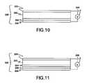
- FIG. 10shows another embodiment of an OELD including a hole injection enhancement layer.
- FIG. 11shows another embodiment of an OELD including a hole injection enhancement layer and a hole transport layer.
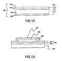
- FIG. 12shows another embodiment of an OELD including an electron injecting and transporting layer.
- FIG. 13shows an OELD sealed between a substrate having a graded-composition barrier coating and a reflective layer.
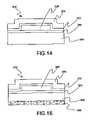
- FIG. 14shows an OELD sealed between two substrates, each having a graded-composition barrier coating.
- FIG. 15shows a sealed OELD having a light conversion layer.
- the present inventionin one aspect, provides a substrate having at least a coating disposed on a surface thereof, which coating is capable of reducing diffusion rates of chemical species through the substrate.
- the coatingcomprises a material, the composition of which varies across a thickness thereof.
- Such a coated substratefinds uses in providing protection to many devices or components; e.g., electronic devices, that are susceptible to reactive chemical species normally encountered in the environment.
- such a substrate or film having a diffusion-barrier coating having graded compositioncan advantageously be used in packaging of materials, such as foodstuff, that are easily spoiled by chemical or biological agents normally existing in the environment.
- Organic light-emitting material and/or cathode materials in OELDsare susceptible to attack by reactive species existing in the environment, such as oxygen, water vapor, hydrogen sulfide, SO x , NO x , solvents, etc. Films having a graded-composition diffusion-barrier coating are particularly useful to extend the life of these devices and render them more commercially viable.
- a barrier coating of the present inventionmay be made by depositing reaction or recombination products of reacting species onto a substrate or film. Varying the relative supply rates or changing the identities of the reacting species results in a coating that has a graded composition across its thickness. Thus, a coating of the present invention does not have distinct interfaces at which the composition of the coating changes abruptly.
- Substrate materials that benefit from having a graded-composition diffusion-barrier coatingare organic polymeric materials; such as polyethyleneterephthalate (“PET”); polyacrylates; polycarbonate; silicone; epoxy resins; silicone-functionalized epoxy resins; polyester such as Mylar (made by E. I.
- du Pont de Nemours & Co.polyimide such as Kapton H or Kapton E (made by du Pont), Apical AV (made by Kanegafugi Chemical Industry Company), Upilex (made by UBE Industries, Ltd.); polyethersulfones (“PES,” made by Sumitomo); polyetherimide such as Ultem (made by General Electric Company); and polyethylenenaphthalene (“PEN”).
- polyimidesuch as Kapton H or Kapton E (made by du Pont), Apical AV (made by Kanegafugi Chemical Industry Company), Upilex (made by UBE Industries, Ltd.); polyethersulfones (“PES,” made by Sumitomo); polyetherimide such as Ultem (made by General Electric Company); and polyethylenenaphthalene (“PEN”).
- Kapton H or Kapton Emade by du Pont
- Apical AVmade by Kanegafugi Chemical Industry Company
- Upilexmade by UBE Industries, Ltd.
- PESpolyethersulfones
- Ultemmade by General
- Suitable coating compositions of regions across the thicknessare organic, inorganic, or ceramic materials. These materials are typically reaction or recombination products of reacting plasma species and are deposited onto the substrate surface.
- Organic coating materialstypically comprise carbon, hydrogen, oxygen, and optionally other minor elements, such as sulfur, nitrogen, silicon, etc., depending on the types of reactants.
- Suitable reactants that result in organic compositions in the coatingare straight or branched alkanes, alkenes, alkynes, alcohols, aldehydes, ethers, alkylene oxides, aromatics, etc., having up to 15 carbon atoms.
- Inorganic and ceramic coating materialstypically comprise oxide; nitride; carbide; boride; or combinations thereof of elements of Groups IIA, IIIA, IVA, VA, VIA, VIIA, IB, and IIB; metals of Groups IIIB, IVB, and VB; and rare-earth metals.
- silicon carbidecan be deposited onto a substrate by recombination of plasmas generated from silane (SiH 4 ) and an organic material, such as methane or xylene.
- Silicon oxycarbidecan be deposited from plasmas generated from silane, methane, and oxygen or silane and propylene oxide.
- Silicon oxycarbidealso can be deposited from plasmas generated from organosilicone precursors, such as tetraethoxysilane (TEOS), hexamethyldisiloxane (HMDSO), hexamethyldisilazane (HMDSN), or octamethylcyclotetrasiloxane (D4).
- TEOStetraethoxysilane
- HMDSOhexamethyldisiloxane
- HMDSNhexamethyldisilazane
- D4octamethylcyclotetrasiloxane
- Silicon nitridecan be deposited from plasmas generated from silane and ammonia.
- Aluminum oxycarbonitridecan be deposited from a plasma generated from a mixture of aluminum tartrate and ammonia.
- Other combinations of reactantsmay be chosen to obtain a desired coating composition. The choice of the particular reactants is within the skills of the artisans.
- Coating thicknessis typically in the range from about 10 nm to about 10000 nm, preferably from about 10 nm to about 1000 nm, and more preferably from about 10 nm to about 200 nm. It may be desired to choose a coating thickness that does not impede the transmission of light through the substrate, such as a reduction in light transmission being less than about 20 percent, preferably less than about 10 percent, and more preferably less than about 5 percent.
- the coatingmay be formed by one of many deposition techniques, such as plasma-enhanced chemical-vapor deposition (“PECVD”), radio-frequency plasma-enhanced chemical-vapor deposition (“RFPECVD”), expanding thermal-plasma chemical-vapor deposition (“ETPCVD”), sputtering including reactive sputtering, electron-cyclotron-resonance plasma-enhanced chemical-vapor deposition (“ECRPECVD”), inductively coupled plasma-enhanced chemical-vapor deposition (“ICPECVD”), or combinations thereof.
- PECVDplasma-enhanced chemical-vapor deposition
- RFPECVDradio-frequency plasma-enhanced chemical-vapor deposition
- EPCVDexpanding thermal-plasma chemical-vapor deposition
- sputtering including reactive sputteringincluding reactive sputtering
- ECRPECVDelectron-cyclotron-resonance plasma-enhanced chemical-vapor deposition
- ICPECVDinductively coupled plasma-enh
- FIG. 1schematically illustrates a reactor 10 and associated equipment for the ETPCVD technique.
- At least one cathode 20typically made of tungsten, is disposed in a cathode housing 30 .
- Anode plate 40is disposed at one end of cathode housing 30 .
- at least a cathode housingis electrically floating.
- a voltage applied between cathode 20 and anode 40generates an arc for plasma generation.
- a carrier gas, such as argonis fed through line 50 to the arc.
- a plasmais generated and exits a nozzle or orifice 70 at the center of anode 40 .
- a first reactant gascan be fed through line 60 into the carrier gas line at a point between cathode 20 and anode 40 .
- a second reactant gasis fed through supply line 80 to a point downstream from orifice 70 .
- Supply line 80may also terminate with a perforated ring disposed within expanding plasma beam 84 for better mixing.
- Other reactant supply linescan be provided for different reactant species. Radicals are generated from reactant gases, combined, carried to substrate 90 , and deposited thereon, which substrate is supported on substrate holder 100 .
- Substrate holder 100is disposed opposite and at a distance from nozzle 70 and is movable relative to nozzle 70 by substrate-holder shaft 110 .
- Reactor 10is kept under vacuum via vacuum connection 112 .
- the first reactant gascan be ammonia
- the second reactant gascan be silane.
- the relative supply rates of first and second reactant gasesare varied during deposition to vary the composition of the deposited material as the coating is built up.
- FIG. 1schematically shows a substrate as a single piece 90
- a coatingmay be deposited on a continuous substrate in similar equipment.
- FIG. 2shows a supply roll 120 of a thin polymeric substrate 115 , which supply roll 120 is disposed on one side of substrate holder 100 , and a take-up roll 122 disposed on the other side of substrate holder 100 .
- uncoated substrate film 115continuously receives the coating material as it passes over substrate holder 100 .
- substrate film 115passes through an area opposite to many overlapping plasma beams, each being generated with different or varying compositions to receive a coating, the composition of which varies continuously though its thickness.
- the plasmais generated at a high pressure compared to the regular PECVD technique.
- the plasma in arc channel 65has a velocity on the order of sound velocity.
- the plasmaexpands supersonically into reactor chamber 10 via nozzle 70 and moves subsonically toward substrate 90 .
- FIG. 3schematically shows reactor 200 and associated equipment for the RFPECVD technique.
- Radio frequency (“RF”) poweris applied to cathode 210 , which is disposed in reactor 200 , by RF generator and amplifier 204 and matching network 208 , which comprises a plurality of electrical and/or electronic components for generating appropriate impedance or other electrical characteristics of the overall system to maximize power transfer from RF generator and amplifier 204 .
- Substrate 90is disposed on substrate holder 100 opposite to cathode 210 to receive plasma deposition.
- Substrate holdermay be grounded or electrically coupled to another RF generator and matching network, if a different potential is desired.
- a reactant gas or a mixture of gasesis fed into a gas distributor 212 through a gas supply 214 .
- Gas distributor 212may have any shape that promotes a substantially uniform distribution of gases. For example, it may be a ring having perforations directed toward substrate holder 100 . Alternatively, cathode 210 may itself be hollow and porous and receives reactant gases. A plasma is generated and maintained by the RF field and flows toward substrate 90 . Precursor species in the plasma are combined and deposited on substrate 90 . The composition of the coating can be varied while it is built up by varying the composition of the reactant gas mixture fed into distributor 212 . A continuous substrate such as a polymeric film may be coated with a graded-composition coating by providing an unwinding supply roll and a take-up roll, as described above. The substrate likewise can travel opposite to a plurality of deposition stations, which supply varying gas compositions, to produce a continuous film having a graded-composition coating.
- ECRPECVDis another suitable deposition technique. This method operates at low pressure, typically less than about 0.5 mm Hg, and typically without electrodes. A discharge is generated by microwave. A magnetic field is used to create the resonance condition of the electron gas, which results in a very high degree of ionization due to electron acceleration at a distance away from the substrate. The low pressure preserves a high number density of free radicals until the plasma reaches the substrate and prevents normally undesirable severe bombardment thereof.
- ICPECVDis another electrodeless deposition technique that can create high-density plasma at low pressure.
- a plasmais generated by an electromagnetic field generated by a concentric induction coil disposed outside one end of the deposition chamber.
- the substrateis disposed in the deposition chamber at the opposite end.
- Depositioncan typically be carried out at pressure much less than 0.5 mm Hg.
- the energy of the ions in a plasmamay be controlled such that they penetrate into a surface layer of the substrate to create a diffuse transition region between the composition of the bulk substrate and the composition of the coating. Such a transition prevents an abrupt change in the composition and mitigates any chance for delamination of the coating.
- a graded-composition coating having a thickness of about 500 nmwas formed on a polycarbonate substrate having a dimension of about 10 cm ⁇ 10 cm and a thickness of about 0.2 mm using the RFPECVD technique and tested for water vapor and oxygen transmission.
- Silanemaximum flow rate of about 500 standard cm 3 /minute
- ammoniamaximum flow rate of about 60 standard cm 3 /minute
- propylene oxidemaximum flow rate of about 500 standard cm 3 /minute
- the power fed to the RF electrodewas about 100 W when plasma was generated from propylene oxide, and about 200 W when a mixture of silane and ammonia was fed into the reactor.
- the vacuum level in the reactorwas about 0.2 mm Hg and the average temperature was about 55° C.
- FIG. 4shows the elemental composition of the coating, as measured by dynamic XPS, as a function of sputtering time to remove portions of the thickness of the coating during the dynamic XPS testing, which is directly related to the depth of the coating.
- Oxygen and water vapor transmission test resultsare shown in FIGS. 5 and 6 .
- the oxygen transmission rate through the coated plastic substratewas reduced by over three orders of magnitude compared to the uncoated substrate, and the water vapor transmission rate by over two orders of magnitude.
- Light transmission at various wavelengths of the visible spectrum through the coated substrateis shown in FIG. 7 .
- the reduction in light transmission in the blue to red regionwas generally less than 7 percent.
- a plastic substrate coated with a graded-composition coatingwhich is formed by any method disclosed above can be advantageously used to produce flexible light sources based on organic light-emitting materials.
- Other electronic devices that can benefit from the protection afforded by a graded-composition coatingare, for example, displays including liquid crystal displays, photovoltaic devices, flexible integrated circuits, or components of medical diagnostic systems.
- the term “flexible”means being capable of being bent into a shape having a radius of curvature of less than about 100 cm.
- substantially transparentmeans allowing a total transmission of at least about 50 percent, preferably at least about 80 percent, and more preferably at least 90 percent, of light in the visible range (i.e., having wavelength in the range from about 400 nm to about 700 nm). It should be understood that the composition of a graded-composition barrier coating does not necessarily vary monotonically from one surface to the other surface thereof. A monotonically varying composition is only one case of graded-composition for the barrier of the present invention.
- FIG. 8is a schematic diagram of an embodiment of the present invention. It should be understood that the figures accompanying this disclosure are not drawn to scale.
- OELD or a light-emitting device 310comprises an organic EL member 320 disposed on a substantially transparent substrate 340 having a graded-composition barrier coating 350 , as described above.
- the graded-composition barrier coating 350may be disposed or otherwise formed on either or both of the surfaces of the substrate 340 adjacent to the organic EL member 320 .
- the graded-composition barrier coating 350is disposed or formed on the surface of the substrate 340 adjacent to the organic EL member 320 or it may completely cover the substrate 340 .
- FIG. 8shows schematically a distinct interface between substrate 340 and coating 350 , such a coating may be formed such that there is no sharp interface therebetween, as described above.
- Substrate 340may be a single piece or a structure comprising a plurality of adjacent pieces of different materials and has an index of refraction (or refractive index) in the range from about 1.05 to about 2.5, preferably from about 1.1 to about 1.6.
- substrate 340is made of a substantially transparent polymeric material.
- suitable polymeric materialsare polyethylenterephathalate (“PET”), polyacrylates, polycarbonate, silicone, epoxy resins, silicone-functionalized epoxy resins, polyester, polyimide, polyetherimide, PES, PEN, polynorbonenes, or poly (cyclic olefins).
- Light-emitting member 320comprises at least one layer 330 of at least one organic EL material sandwiched between two electrodes 322 and 338 , as shown in FIG. 9 .
- the light-emitting membermay comprise one or more additional layers between an electrode and the layer 330 of organic EL material.
- electrode 322is a cathode injecting negative charge carriers (electrons) into organic EL layer 330 and is made of a material having a low work function; e.g., less than about 4 eV.
- Low-work function materials suitable for use as a cathodeare K, Li, Na, Mg, La, Ce, Ca, Sr, Ba, Al, Ag, In, Sn, Zn, Zr, Sm, Eu, alloys thereof, or mixtures thereof.
- Preferred materials for the manufacture of cathode layer 322are Ag—Mg, Al—Li, In—Mg, and Al—Ca alloys.
- Layered non-alloy structuresare also possible, such as a thin layer of a metal such as Ca (thickness from about 1 to about 10 nm) or a non-metal such as LiF, covered by a thicker layer of some other metal, such as aluminum or silver.
- electrode 338is an anode injecting positive charge carriers (or holes) into organic layer 330 and is made of a material having a high work function; e.g., greater than about 4.5 eV, preferably from about 5 eV to about 5.5 eV.
- Indium tin oxide (“ITO”)is typically used for this purpose. ITO is substantially transparent to light transmission and allows at least 80% light transmitted therethrough. Therefore, light emitted from organic electroluminescent layer 330 can easily escape through the ITO anode layer without being seriously attenuated.
- Other materials suitable for use as the anode layerare tin oxide, indium oxide, zinc oxide, indium zinc oxide, cadmium tin oxide, and mixtures thereof.
- Electrode layers 322 and 338may be deposited on the underlying element by physical vapor deposition, chemical vapor deposition, ion beam-assisted deposition, or sputtering. A thin, substantially transparent layer of a metal is also suitable.
- Electrode layers 322 and 338may serve as the anode and cathode, respectively.
- the thickness of the cathode layerin this case is about 200 nm.
- Organic EL layer 330serves as the transport medium for both holes and electrons. In this layer these excited species combine and drop to a lower energy level, concurrently emitting EM radiation in the visible range.
- Organic EL materialsare chosen to electroluminesce in the desired wavelength range. The thickness of the organic EL layer 330 is preferably kept in the range of about 100 to about 300 nm.
- the organic EL materialmay be a polymer, a copolymer, a mixture of polymers, or lower molecular-weight organic molecules having unsaturated bonds. Such materials possess a delocalized ⁇ -electron system, which gives the polymer chains or organic molecules the ability to support positive and negative charge carriers with high mobility.
- Suitable EL polymersare poly(N-vinylcarbazole) (“PVK”, emitting violet-to-blue light in the wavelengths of about 380–500 nm); poly(alkylfluorene) such as poly (9,9-dihexylfluorene) (410–550 nm), poly(dioctylfluorene) (wavelength at peak EL emission of 436 nm), or poly ⁇ 9,9-bis(3,6-dioxaheptyl)-fluorene-2,7-diyl ⁇ (400–550 nm); poly(praraphenylene) derivatives such as poly(2-decyloxy-1,4-phenylene) (400–550 nm). Mixtures of these polymers or copolymers based on one or more of these polymers and others may be used to tune the color of emitted light.
- PVKpoly(N-vinylcarbazole)
- polysilanesare linear silicon-backbone polymers substituted with a variety of alkyl and/or aryl side groups. They are quasi one-dimensional materials with delocalized ⁇ -conjugated electrons along polymer backbone chains. Examples of polysilanes are poly(di-n-butylsilane), poly(di-n-pentylsilane), poly(di-n-hexylsilane), poly(methylphenylsilane), and poly ⁇ bis (p-butylphenyl)silane ⁇ which are disclosed in H.
- Organic materials having molecular weight less than about 5000 that are made of a large number of aromatic unitsare also applicable.
- An example of such materialsis 1,3,5-tris ⁇ n-(4-diphenylaminophenyl) phenylamino ⁇ benzene, which emits light in the wavelength range of 380–500 nm.
- the organic EL layeralso may be prepared from lower molecular weight organic molecules, such as phenylanthracene, tetraarylethene, coumarin, rubrene, tetraphenylbutadiene, anthracene, perylene, coronene, or their derivatives. These materials generally emit light having maximum wavelength of about 520 nm.
- Still other suitable materialsare the low molecular-weight metal organic complexes such as aluminum-, gallium-, and indium-acetylacetonate, which emit light in the wavelength range of 415–457 nm, aluminum-(picolymethylketone)-bis ⁇ 2,6-di(t-butyl)phenoxide ⁇ or scandium-(4-methoxy-picolylmethylketone)-bis (acetylacetonate), which emits in the range of 420–433 nm.
- the preferred organic EL materialsare those emit light in the blue-green wavelengths.
- More than one organic EL layermay be formed successively one on top of another, each layer comprising a different organic EL material that emits in a different wavelength range. Such a construction can facilitate a tuning of the color of the light emitted from the overall light-emitting device 310 .
- one or more additional layersmay be included in light-emitting member 320 to increase the efficiency of the overall device 310 .
- these additional layerscan serve to improve the injection (electron or hole injection enhancement layers) or transport (electron or hole transport layers) of charges into the organic EL layer.
- the thickness of each of these layersis kept to below 500 nm, preferably below 100 nm.
- Materials for these additional layersare typically low-to-intermediate molecular weight (less than about 2000) organic molecules. They may be applied during the manufacture of the device 310 by conventional methods such as spray coating, dip coating, or physical or chemical vapor deposition. In one embodiment of the present invention, as shown in FIG.
- a hole injection enhancement layer 336is formed between the anode layer 338 and the organic EL layer 330 to provide a higher injected current at a given forward bias and/or a higher maximum current before the failure of the device.
- the hole injection enhancement layerfacilitates the injection of holes from the anode.
- Suitable materials for the hole injection enhancement layerare arylene-based compounds disclosed in U.S. Pat. No. 5,998,803; such as 3,4,9,10-perylenetetra-carboxylic dianhydride or bis (1,2,5-thiadiazolo)-p-quinobis(1,3-dithiole).
- light-emitting member 320further includes a hole transport layer 334 which is disposed between the hole injection enhancement layer 336 and the organic EL layer 330 .
- the hole transport layer 334has the functions of transporting holes and blocking the transportation of electrons so that holes and electrons are optimally combined in the organic EL layer 330 .
- Materials suitable for the hole transport layerare triaryldiamine, tetraphenyldiamine, aromatic tertiary amines, hydrazone derivatives, carbazole derivatives, triazole derivatives, imidazole derivatives, oxadiazole derivatives having an amino group, and polythiophenes as disclosed in U.S. Pat. No. 6,023,371, which is incorporated herein by reference.
- light-emitting member 320includes an additional layer 324 which is disposed between the cathode layer 322 and the organic EL layer 330 .
- Layer 324has the combined function of injecting and transporting electrons to the organic EL layer 330 .
- Materials suitable for the electron injecting and transporting layerare metal organic complexes such as tris(8-quinolinolato)aluminum, oxadiazole derivatives, perylene derivatives, pyridine derivatives, pyrimidine derivatives, quinoline derivatives, quinoxaline derivatives, diphenylquinone derivatives, and nitro-substituted fluorene derivatives, as disclosed in U.S. Pat. No. 6,023,371, which is incorporated herein by reference.
- a reflective metal layer 360may be disposed on organic EL member 320 to reflect any radiation emitted away from the substantially transparent substrate 340 and direct such radiation toward the substrate 340 such that the total amount of radiation emitted in this direction is increased.
- Reflective metal layer 360also serves an additional function of preventing diffusion of reactive environmental elements, such as oxygen and water vapor, into the organic EL element 320 . Such a diffusion otherwise can degrade the long-term performance of the OELD.
- Suitable metals for the reflective layer 360are silver, aluminum, and alloys thereof. It may be advantageous to provide a thickness that is sufficient to substantially prevent the diffusion of oxygen and water vapor, as long as the thickness does not substantially reduce the flexibility of the entire device.
- one or more additional layers of at least a different materialmay be formed on the reflective layer to further reduce the rate of diffusion of oxygen and water vapor into the organic EL member.
- the material for such additional layer or layersneed not be a reflective material.
- Compounds, such as metal oxides, nitrides, carbides, oxynitrides, or oxycarbides,may be useful for this purpose.
- a bonding layer 358 of a substantially transparent organic polymeric materialmay be disposed on the organic EL member 320 before the reflective metal layer 360 is deposited thereon.
- materials suitable for forming the organic polymeric layerare polyacrylates such as polymers or copolymers of acrylic acid, methacrylic acid, esters of these acids, or acylonitrile; poly(vinyl fluoride); poly(vinylidene chloride); poly(vinyl alcohol); copolymer of vinyl alcohol and glyoxal (also known as ethanedial or oxaaldehyde); polyethyleneterephthalate, parylene (thermoplastic polymer based on p-xylene), and polymers derived from cycloolefins and their derivatives (such as poly (arylcyclobutene) disclosed in U.S. Pat. Nos. 4,540,763 and 5,185,391 which are incorporated herein by reference).
- cycloolefins and their derivativessuch as poly
- a second polymeric substrate 370 having a graded-composition barrier coating 372is disposed on organic EL member 320 opposite to substrate 340 to form a complete seal around organic EL member 320 .
- Graded-composition barrier coating 372may be disposed on either side of substrate 370 . It may be preferred to dispose graded-composition barrier coating 372 adjacent to organic EL member 320 .
- Second polymeric substrate 370 having graded-composition barrier coating 372may also be disposed on reflective metal layer 360 to provide even more protection to organic EL member 320 .
- graded-composition barrier 372may be deposited directly on organic EL member 320 instead of being disposed on a second polymeric substrate (such as 370 ). In this case, the second substrate (such as 370 ) may be eliminated.
- second substrate 370 having graded-composition barrier coating 372can be disposed between organic EL member 320 and reflector layer 360 .
- This configurationmay be desirable when it can offer some manufacturing or cost advantage, especially when the transparency of coated substrate 370 is also substantial.
- the light-emitting device 310further comprises a light-scattering material disposed in the path of light emitted from the light-emitting device 310 to provide more uniform light therefrom.
- FIG. 15illustrates an embodiment comprising a layer 390 of scattering material disposed on the substrate 340 .
- the light-scattering materialis provided by choosing particles that range in size from about 10 nm to about 100 micrometers.
- a preferred embodimentincludes particles about 4 micrometers in size.
- the particle sizeis preferably on the order of 50–65 nm.
- Particles of the light-scattering materialmay be advantageously dispersed in a substantially transparent polymeric film-forming material such as those disclosed above, and the mixture is formed into a film which may be disposed on the substrate 340 .
- Suitable light-scattering materialsare solids having refractive index higher than that of the film forming material. Since typical film forming materials have refractive indices between about 1.3 to about 1.6, the particulate scattering material should have a refractive index higher than about 1.6 and should be optically transparent over the target wavelength range. In addition, it is preferable that the light scattering material be non-toxic and substantially resistant to degradation upon exposure to normal ambient environments.
- suitable light-scattering materialsare rutile (TiO 2 ), hafnia (HfO 2 ), zirconia(ZrO 2 ), zircon (ZrO 2 .SiO 2 ), gadolinium gallium garnet (Gd 3 Ga 5 O 12 ), barium sulfate, yttria (Y 2 O 3 ), yttrium aluminum garnet (“YAG”, Y 3 Al 5 O 12 ), calcite (CaCO 3 ), sapphire (Al 2 O 3 ), diamond, magnesium oxide, germanium oxide.
- Scattering of lightmay also be achieved with a plastic or glass film having a roughened or textured surface (a “diffuser film”), the roughened features of which are typically on the order of a fraction of the wavelength of the scattered light.
- a diffuser filma roughened or textured surface
- one surface of the substratecan be textured or roughened to promote light scattering.
- the light-scattering particles in layer 390can comprise a photoluminescent (“PL”) material (or also herein called a “phosphor”), which is capable of absorbing a portion of the EM radiation emitted by the organic EL member having a first wavelength range and emitting EM radiation having a second wavelength range.
- PLphotoluminescent
- inclusion of such a PL materialcan provide a tuning of color of light emitted from the OELD.
- the particle size and the interaction between the surface of the particle and the polymeric mediumdetermine how well particles are dispersed in polymeric materials to form the film or layer 390 .
- micrometer-sized particles of oxide materialssuch as zirconia, yttrium and rare-earth garnets, and halophosphates, disperse well in standard silicone polymers, such as poly(dimethylsiloxanes) by simple stirring.
- other dispersant materialssuch as a surfactant or a polymeric material like poly(vinyl alcohol)
- the phosphor particlesmay be prepared from larger pieces of phosphor material by any grinding or pulverization method, such as ball milling using zirconia-toughened balls or jet milling. They also may be prepared by crystal growth from solution, and their size may be controlled by terminating the crystal growth at an appropriate time.
- the preferred phosphor materialsefficiently absorb EM radiation emitted by the organic EL material and re-emit light in another spectral region.
- Such a combination of the organic EL material and the phosphorallows for a flexibility in tuning the color of light emitted by the light-emitting device 310 .
- a particular phosphor material or a mixture of phosphorsmay be chosen to emit a desired color or a range of color to complement the color emitted by the organic EL material and that emitted by the organic PL materials.
- An exemplary phosphoris the cerium-doped yttrium aluminum oxide Y 3 Al 5 O 12 garnet (“YAG:Ce”).
- Suitable phosphorsare based on YAG doped with more than one type of rare earth ions, such as (Y 1 ⁇ x ⁇ y Gd x Ce y ) 3 Al 5 O 12 (“YAG:Gd, Ce”), (Y 1 ⁇ x Ce x ) 3 (Al 1 ⁇ y Ga y )O 12 (“YAG:Ga, Ce”), (Y 1 ⁇ x ⁇ y Gd x Ce y )(Al 5 ⁇ z Ga z )O 12 (“YAG:Gd, Ga, Ce”), and (Gd 1 ⁇ x Ce x )Sc 2 Al 3 O 12 (“GSAG”) where 0 ⁇ x ⁇ 1, 0 ⁇ y ⁇ 1, 0 ⁇ z ⁇ 5 and x+y ⁇ 1.
- rare earth ionssuch as (Y 1 ⁇ x ⁇ y Gd x Ce y ) 3 Al 5 O 12 (“YAG:Gd, Ce”), (Y 1 ⁇ x Ce x ) 3 (Al 1 ⁇ y Ga y )O 12 (“YAG:Ga, Ce
- the YAG:Gd, Ce phosphorshows an absorption of light in the wavelength range from about 390 nm to about 530 nm (i.e., the blue-green spectral region) and an emission of light in the wavelength range from about 490 nm to about 700 nm (i.e., the green-to-red spectral region).
- Related phosphorsinclude Lu 3 Al 5 O 12 and Tb 2 Al 5 O 12 , both doped with cerium.
- these cerium-doped garnet phosphorsmay also be additionally doped with small amounts of Pr (such as about 0.1–2 mole percent) to produce an additional enhancement of red emission.
- Prsuch as about 0.1–2 mole percent
- Green-emitting phosphorsCa 8 Mg(SiO 4 ) 4 Cl 2 :Eu 2+ , Mn 2+ ; GdBO 3 :Ce 3+ , Tb 3+ ; CeMgAl 11 O 19 :Tb 3+ ; Y 2 SiO 5 :Ce 3+ , Tb 3+ ; and BaMg 2 Al 16 O 27 :Eu 2+ , Mn 2+ .
- Red-emitting phosphorsY 2 O 3 :Bi 3+ , Eu 3+ ;Sr 2 P 2 O 7 :Eu 2+ , Mn 2+ ; SrMgP 2 O 7 :Eu 2+ , Mn 2+ ;(Y,Gd)(V,B)O 4 :Eu 3+ ; and 3.5MgO.0.5MgF 2 .GeO 2 : Mn 4+ (magnesium fluorogermanate).
- Blue-emitting phosphorsBaMg 2 Al 16 O 27 :Eu 2+ ;Sr 5 (PO 4 ) 10 Cl 2 :Eu 2+ ; and (Ba,Ca,Sr) 5 (PO 4 ) 10 (Cl,F) 2 :Eu 2+ ,(Ca,Ba,Sr)(Al,Ga) 2 S 4 :Eu 2+ .
- Yellow-emitting phosphors(Ba,Ca,Sr) 5 (PO 4 ) 10 (Cl,F) 2 :Eu 2+ , Mn 2+ .
- Still other ionsmay be incorporated into the phoshor to transfer energy from the light emitted from the organic material to other activator ions in the phosphor host lattice as a way to increase the energy utilization.
- Sb 3+ and Mn 2+ ionsexist in the same phosphor lattice, Sb 3+ efficiently absorbs light in the blue region, which is not absorbed very efficiently by Mn 2+ , and transfers the energy to Mn 2+ ion.
- a larger total amount of light emitted by the organic EL materialis absorbed by both ions, resulting in higher quantum efficiency of the total device.
- the photoluminescent materialmay also be an organic dye that can absorb radiation emitted by the organic EL material and emit electromagnetic radiation in the visible spectrum.
- the phosphor particlesare dispersed in a film-forming polymeric material, such as polyacrylates, substantially transparent silicone or epoxy.
- a phosphor composition of less than about 30, preferably less than about 10, percent by volume of the mixture of polymeric material and phosphoris used.
- a solventmay be added into the mixture to adjust the viscosity of the film-forming material to a desired level.
- the mixture of the film-forming material and phosphor particlesis formed into a layer by spray coating, dip coating, printing, or casting on a substrate. Thereafter, the film is removed from the substrate and disposed on the light-emitting member 320 .
- the thickness of film or layer 390is preferably less than 1 mm, more preferably less than 500 ⁇ m.
- the film-forming polymeric materialshave refractive indices close to those of the substrate 340 and the organic EL material; i.e., in the range from about 1.4 to about 1.6.
- scattering film 390may be a diffuser film, which is a plastic film having a roughened surface.
- a method of making an OELD of the present inventionis now described.
- a cleaned flexible substratesuch as a plastic, is first provided.
- a graded-composition barrier coatingis formed on at least a surface of the flexible substrate by a one of many deposition techniques disclosed above.
- a first electrically conducting materialis deposited on the graded-composition barrier coating to form a first electrode of the organic EL member 320 .
- the first electrodemay be deposited on the surface of the substrate 340 that has not been coated with graded-composition barrier coating.
- the first electrodemay be an anode or a cathode, and one or more appropriate materials are chosen among those disclosed earlier for the electrodes.
- the first electrodeis an anode comprising a transparent metal oxide, such as ITO.
- the first electrode materialpreferably sputter-deposited on the substrate.
- the first electrodemay be patterned to a desired configuration by, for example, etching.
- At least one organic EL materialis deposited on the first electrode by physical or chemical vapor deposition, spin coating, dip coating, spraying, printing, or casting, followed by polymerization, if necessary, or curing of the material.
- the organic EL materialmay be diluted in a solvent to adjust its viscosity or mixed with another polymeric material that serves as a film-forming vehicle.
- a second electrically conducting materialis deposited on the at least one organic EL material to form a second electrode.
- the second electrodeis a cathode.
- the second electrodemay be deposited on the entire area of the organic EL material or patterned into a desired shape or configuration. The thickness of the second electrode is kept to a minimum, such as less than or equal to about 200 nm.
- the electrodes and the organic EL materialcomprise the organic EL member 320 .
- a reflective metalis optionally deposited on the surface of the organic EL member 320 opposite to substrate 340 .
- the reflective metalmay be deposited by, for example, sputtering or physical vapor deposition.
- a bonding layer of a substantially transparent materialis deposited on the organic EL member 320 before the layer of reflective metal is deposited thereon.
- the bonding layercomprises an electrically insulating and substantially transparent polymeric material.
- the bonding layermay be deposited by one of the methods disclosed above for deposition of an organic layer.
- the reflective metal layeris formed so as to completely surround the organic EL member 320 .
- the reflective metal layer together with the graded-composition barrier coatingforms a hermetic seal around the organic EL member 20 .
- one or more additional layers of other inorganic materialsmay be deposited on the reflective metal layer.
- a mixture of particles of a scattering or PL material and a transparent polymeric materialis deposited on the surface of the substrate 340 opposite the organic EL member.
- the mixturemay be cast into a tape by a tape casting method, such as the doctor blade method.
- the tapeis then cured and attached to the substrate 340 .
- subsets of layers necessary or desired for the operation of an OELD of the present inventionare formed in separate assemblies, and the assemblies are laminated or attached together to produce a working device.
- a first substrate having a first graded-composition barrier coating, an assembly of an organic EL member, and a second substrate having a second graded-composition barrier coatingare laminated together to provide a light source having improved resistance to attack by chemical species in the environment.
- large-area flexible displays or lighting systemsincorporate OELDs of the present invention.
Landscapes
- Chemical & Material Sciences (AREA)
- Engineering & Computer Science (AREA)
- Nanotechnology (AREA)
- Physics & Mathematics (AREA)
- Optics & Photonics (AREA)
- Materials Engineering (AREA)
- Crystallography & Structural Chemistry (AREA)
- Condensed Matter Physics & Semiconductors (AREA)
- General Physics & Mathematics (AREA)
- Mechanical Engineering (AREA)
- Manufacturing & Machinery (AREA)
- Chemical Kinetics & Catalysis (AREA)
- Inorganic Chemistry (AREA)
- Metallurgy (AREA)
- Organic Chemistry (AREA)
- Composite Materials (AREA)
- Life Sciences & Earth Sciences (AREA)
- Biophysics (AREA)
- General Chemical & Material Sciences (AREA)
- Computer Hardware Design (AREA)
- Microelectronics & Electronic Packaging (AREA)
- Power Engineering (AREA)
- Electroluminescent Light Sources (AREA)
- Laminated Bodies (AREA)
- Paints Or Removers (AREA)
- Application Of Or Painting With Fluid Materials (AREA)
Abstract
Description
Claims (29)
Priority Applications (22)
| Application Number | Priority Date | Filing Date | Title |
|---|---|---|---|
| US10/065,018US7015640B2 (en) | 2002-09-11 | 2002-09-11 | Diffusion barrier coatings having graded compositions and devices incorporating the same |
| JP2004536005AJP4690041B2 (en) | 2002-09-11 | 2003-08-06 | Diffusion barrier coating with graded composition and device comprising the same |
| PCT/US2003/024555WO2004025749A2 (en) | 2002-09-11 | 2003-08-06 | Diffusion barrier coatings having graded compositions and devices incorporating the same |
| AU2003258093AAU2003258093A1 (en) | 2002-09-11 | 2003-08-06 | Diffusion barrier coatings having graded compositions and devices incorporating the same |
| SG2011058211ASG2011058211A (en) | 2002-09-11 | 2003-08-06 | Diffusion barrier coatings having graded compositions and devices incorporating the same |
| EP03795589.5AEP1540750B1 (en) | 2002-09-11 | 2003-08-06 | Diffusion barrier coatings having graded compositions and devices incorporating the same |
| CA2497786ACA2497786C (en) | 2002-09-11 | 2003-08-06 | Diffusion barrier coatings having graded compositions and devices incorporating the same |
| SG200701499-6ASG170616A1 (en) | 2002-09-11 | 2003-08-06 | Diffusion barrier coatings having graded compositions and devices inforporting the same |
| EP17207117.7AEP3312893B1 (en) | 2002-09-11 | 2003-08-06 | Diffusion barrier coatings having graded compositions and devices incoroprating the same |
| KR1020057004156AKR101052380B1 (en) | 2002-09-11 | 2003-08-06 | Diffusion barrier coatings having a gradually changing composition and devices comprising the same |
| CNB038250721ACN100530756C (en) | 2002-09-11 | 2003-08-06 | Diffusion barrier coatings having graded compositions and devices incorporating the same |
| TW92124098ATWI361016B (en) | 2002-09-11 | 2003-09-01 | Diffusion barrier coatings having graded compositi |
| US11/188,984US8455041B2 (en) | 2002-09-11 | 2005-07-26 | Diffusion barrier coatings having graded compositions and devices incorporating the same |
| US11/188,983US7154220B2 (en) | 2002-09-11 | 2005-07-26 | Diffusion barrier coatings having graded compositions and devices incorporating the same |
| US11/292,281US7486020B2 (en) | 2002-09-11 | 2005-12-02 | Diffusion barrier coatings having graded compositions and devices incorporating the same |
| US11/376,325US7943205B2 (en) | 2002-09-11 | 2006-03-16 | Diffusion barrier coatings having graded compositions and devices incorporating the same |
| US11/378,480US20060208634A1 (en) | 2002-09-11 | 2006-03-20 | Diffusion barrier coatings having graded compositions and devices incorporating the same |
| US11/398,724US7397183B2 (en) | 2002-09-11 | 2006-04-06 | Diffusion barrier coatings having graded compositions and devices incorporating the same |
| US11/828,543US8691371B2 (en) | 2002-09-11 | 2007-07-26 | Barrier coating and method |
| US12/124,548US8227984B2 (en) | 2002-09-11 | 2008-05-21 | Barrier coatings |
| US12/124,631US20090022907A1 (en) | 2002-09-11 | 2008-05-21 | Barrier coatings |
| US12/267,399US8383214B2 (en) | 2002-09-11 | 2008-11-07 | Diffusion barrier coatings having graded compositions and devices incorporating the same |
Applications Claiming Priority (1)
| Application Number | Priority Date | Filing Date | Title |
|---|---|---|---|
| US10/065,018US7015640B2 (en) | 2002-09-11 | 2002-09-11 | Diffusion barrier coatings having graded compositions and devices incorporating the same |
Related Parent Applications (1)
| Application Number | Title | Priority Date | Filing Date |
|---|---|---|---|
| US11/398,724Continuation-In-PartUS7397183B2 (en) | 2002-09-11 | 2006-04-06 | Diffusion barrier coatings having graded compositions and devices incorporating the same |
Related Child Applications (6)
| Application Number | Title | Priority Date | Filing Date |
|---|---|---|---|
| US10/779,373Continuation-In-PartUS20050181212A1 (en) | 2002-09-11 | 2004-02-17 | Composite articles having diffusion barriers and devices incorporating the same |
| US11/188,983DivisionUS7154220B2 (en) | 2002-09-11 | 2005-07-26 | Diffusion barrier coatings having graded compositions and devices incorporating the same |
| US11/188,984DivisionUS8455041B2 (en) | 2002-09-11 | 2005-07-26 | Diffusion barrier coatings having graded compositions and devices incorporating the same |
| US11/292,281ContinuationUS7486020B2 (en) | 2002-09-11 | 2005-12-02 | Diffusion barrier coatings having graded compositions and devices incorporating the same |
| US11/376,325ContinuationUS7943205B2 (en) | 2002-09-11 | 2006-03-16 | Diffusion barrier coatings having graded compositions and devices incorporating the same |
| US11/378,480Continuation-In-PartUS20060208634A1 (en) | 2002-09-11 | 2006-03-20 | Diffusion barrier coatings having graded compositions and devices incorporating the same |
Publications (2)
| Publication Number | Publication Date |
|---|---|
| US20040046497A1 US20040046497A1 (en) | 2004-03-11 |
| US7015640B2true US7015640B2 (en) | 2006-03-21 |
Family
ID=31989951
Family Applications (7)
| Application Number | Title | Priority Date | Filing Date |
|---|---|---|---|
| US10/065,018Expired - LifetimeUS7015640B2 (en) | 2002-09-11 | 2002-09-11 | Diffusion barrier coatings having graded compositions and devices incorporating the same |
| US11/188,983Expired - LifetimeUS7154220B2 (en) | 2002-09-11 | 2005-07-26 | Diffusion barrier coatings having graded compositions and devices incorporating the same |
| US11/188,984Active2028-09-12US8455041B2 (en) | 2002-09-11 | 2005-07-26 | Diffusion barrier coatings having graded compositions and devices incorporating the same |
| US11/292,281Expired - LifetimeUS7486020B2 (en) | 2002-09-11 | 2005-12-02 | Diffusion barrier coatings having graded compositions and devices incorporating the same |
| US11/376,325Expired - LifetimeUS7943205B2 (en) | 2002-09-11 | 2006-03-16 | Diffusion barrier coatings having graded compositions and devices incorporating the same |
| US11/398,724Expired - LifetimeUS7397183B2 (en) | 2002-09-11 | 2006-04-06 | Diffusion barrier coatings having graded compositions and devices incorporating the same |
| US12/267,399Expired - LifetimeUS8383214B2 (en) | 2002-09-11 | 2008-11-07 | Diffusion barrier coatings having graded compositions and devices incorporating the same |
Family Applications After (6)
| Application Number | Title | Priority Date | Filing Date |
|---|---|---|---|
| US11/188,983Expired - LifetimeUS7154220B2 (en) | 2002-09-11 | 2005-07-26 | Diffusion barrier coatings having graded compositions and devices incorporating the same |
| US11/188,984Active2028-09-12US8455041B2 (en) | 2002-09-11 | 2005-07-26 | Diffusion barrier coatings having graded compositions and devices incorporating the same |
| US11/292,281Expired - LifetimeUS7486020B2 (en) | 2002-09-11 | 2005-12-02 | Diffusion barrier coatings having graded compositions and devices incorporating the same |
| US11/376,325Expired - LifetimeUS7943205B2 (en) | 2002-09-11 | 2006-03-16 | Diffusion barrier coatings having graded compositions and devices incorporating the same |
| US11/398,724Expired - LifetimeUS7397183B2 (en) | 2002-09-11 | 2006-04-06 | Diffusion barrier coatings having graded compositions and devices incorporating the same |
| US12/267,399Expired - LifetimeUS8383214B2 (en) | 2002-09-11 | 2008-11-07 | Diffusion barrier coatings having graded compositions and devices incorporating the same |
Country Status (10)
| Country | Link |
|---|---|
| US (7) | US7015640B2 (en) |
| EP (2) | EP3312893B1 (en) |
| JP (1) | JP4690041B2 (en) |
| KR (1) | KR101052380B1 (en) |
| CN (1) | CN100530756C (en) |
| AU (1) | AU2003258093A1 (en) |
| CA (1) | CA2497786C (en) |
| SG (2) | SG2011058211A (en) |
| TW (1) | TWI361016B (en) |
| WO (1) | WO2004025749A2 (en) |
Cited By (109)
| Publication number | Priority date | Publication date | Assignee | Title |
|---|---|---|---|---|
| US20040018305A1 (en)* | 2002-04-15 | 2004-01-29 | Pagano John Chris | Apparatus for depositing a multilayer coating on discrete sheets |
| US20040119404A1 (en)* | 2002-07-05 | 2004-06-24 | Yoshifumi Kato | Lighting system and display |
| US20050082966A1 (en)* | 2003-10-21 | 2005-04-21 | Shunpei Yamazaki | Light-emitting device |
| US20050176181A1 (en)* | 1999-10-25 | 2005-08-11 | Burrows Paul E. | Method for edge sealing barrier films |
| US20050181212A1 (en)* | 2004-02-17 | 2005-08-18 | General Electric Company | Composite articles having diffusion barriers and devices incorporating the same |
| US20050202646A1 (en)* | 1999-10-25 | 2005-09-15 | Burrows Paul E. | Method for edge sealing barrier films |
| US20050239294A1 (en)* | 2002-04-15 | 2005-10-27 | Rosenblum Martin P | Apparatus for depositing a multilayer coating on discrete sheets |
| US20050260393A1 (en)* | 2004-05-24 | 2005-11-24 | Tsung-Neng Liao | Substrate capable of preventing from warping and having protective layers to prevent from scrubbing |
| US20060003189A1 (en)* | 2004-06-30 | 2006-01-05 | Kim Tae W | Barrier coatings |
| US20060001040A1 (en)* | 2004-06-30 | 2006-01-05 | General Electric Company | High integrity protective coatings |
| US20060078744A1 (en)* | 2004-03-04 | 2006-04-13 | Forhouse Corporation | Substrate having insulating layers to prevent it from warping and the method of making the same |
| US20060132032A1 (en)* | 2002-09-11 | 2006-06-22 | General Electric Company One Research Circle | Diffusion barrier coatings having graded compositions and devices incorporating the same |
| US20060187385A1 (en)* | 2005-02-22 | 2006-08-24 | Chi-Chang Liao | Flexible transflective device and manufacturing method thereof |
| US20060216951A1 (en)* | 2003-04-11 | 2006-09-28 | Lorenza Moro | Method of making an encapsulated sensitive device |
| US20060244370A1 (en)* | 2005-05-02 | 2006-11-02 | Eastman Kodak Company | Light-emitting layer spacing in tandem OLED devices |
| US20070026137A1 (en)* | 2005-07-26 | 2007-02-01 | Seiko Epson Corporation | Method for manufacturing electroluminescence device |
| US20070040501A1 (en)* | 2005-08-18 | 2007-02-22 | Aitken Bruce G | Method for inhibiting oxygen and moisture degradation of a device and the resulting device |
| US20070069233A1 (en)* | 2003-12-19 | 2007-03-29 | Min Yan | Multilayer device and method of making |
| US20070164671A1 (en)* | 2003-10-20 | 2007-07-19 | Semiconductor Energy Laboratory Co., Ltd. | Light-Emitting Device and Method for Manufacturing Light-Emitting Device |
| US20070196682A1 (en)* | 1999-10-25 | 2007-08-23 | Visser Robert J | Three dimensional multilayer barrier and method of making |
| US20070252526A1 (en)* | 2005-08-18 | 2007-11-01 | Aitken Bruce G | Sealing technique for decreasing the time it takes to hermetically seal a device and the resulting hermetically sealed device |
| US20070259466A1 (en)* | 2003-08-29 | 2007-11-08 | Semiconductor Energy Laboratory Co., Ltd. | Light Emitting Element and Manufacturing Method Thereof |
| US20070281174A1 (en)* | 2003-04-11 | 2007-12-06 | Vitex Systems, Inc. | Multilayer barrier stacks and methods of making multilayer barrier stacks |
| US20080006819A1 (en)* | 2006-06-19 | 2008-01-10 | 3M Innovative Properties Company | Moisture barrier coatings for organic light emitting diode devices |
| US20080138624A1 (en)* | 2006-12-06 | 2008-06-12 | General Electric Company | Barrier layer, composite article comprising the same, electroactive device, and method |
| US20080149924A1 (en)* | 2005-08-18 | 2008-06-26 | Bruce Gardiner Aitken | Hermetically sealing a device without a heat treating step and the resulting hermetically sealed device |
| US20080156880A1 (en)* | 2006-12-29 | 2008-07-03 | Symbol Technologies, Inc. | Imaging-based reader having light guided illumination |
| US20080182101A1 (en)* | 2003-05-16 | 2008-07-31 | Peter Francis Carcia | Barrier films for plastic substrates fabricated by atomic layer deposition |
| USRE40531E1 (en) | 1999-10-25 | 2008-10-07 | Battelle Memorial Institute | Ultrabarrier substrates |
| US20080315188A1 (en)* | 2007-06-20 | 2008-12-25 | Tae-Hyung Hwang | Apparatus and method for depositing thin film |
| US20090087998A1 (en)* | 2004-02-20 | 2009-04-02 | Oc Oerlikon Balzers Ag | Diffusion barrier layer and method for manufacturing a diffusion barrier layer |
| US20090110892A1 (en)* | 2004-06-30 | 2009-04-30 | General Electric Company | System and method for making a graded barrier coating |
| US20090121333A1 (en)* | 2006-11-30 | 2009-05-14 | Bruce Gardiner Aitken | Flexible substrates having a thin-film barrier |
| USRE40787E1 (en) | 1999-10-25 | 2009-06-23 | Battelle Memorial Institute | Multilayer plastic substrates |
| US20090162674A1 (en)* | 2007-12-20 | 2009-06-25 | Brett Allen Boutwell | Tapes comprising barrier coating compositions and components comprising the same |
| US20090169770A1 (en)* | 2005-07-20 | 2009-07-02 | 3M Innovative Properties Company | Moisture barrier coatings |
| US20090191342A1 (en)* | 1999-10-25 | 2009-07-30 | Vitex Systems, Inc. | Method for edge sealing barrier films |
| US20090208754A1 (en)* | 2001-09-28 | 2009-08-20 | Vitex Systems, Inc. | Method for edge sealing barrier films |
| US20090215208A1 (en)* | 2006-04-07 | 2009-08-27 | Seth Coe-Sullivan | Composition including material, methods of depositing material, articles including same and systems for depositing material |
| US20090215209A1 (en)* | 2006-04-14 | 2009-08-27 | Anc Maria J | Methods of depositing material, methods of making a device, and systems and articles for use in depositing material |
| US20090226598A1 (en)* | 2008-02-11 | 2009-09-10 | Boston Scientific Scimed, Inc. | Substrate Coating Apparatus Having a Solvent Vapor Emitter |
| US20090258237A1 (en)* | 2008-04-10 | 2009-10-15 | Samsung Electronics Co., Ltd. | Graded composition encapsulation thin film comprising anchoring layer and method of fabricating the same |
| US20090283742A1 (en)* | 2006-06-24 | 2009-11-19 | Seth Coe-Sullivan | Methods and articles including nanomaterial |
| US20090286010A1 (en)* | 2008-05-16 | 2009-11-19 | General Electric Company | High throughput processes and systems for barrier film deposition and/or encapsulation of optoelectronic devices |
| US20090283778A1 (en)* | 2006-09-12 | 2009-11-19 | Seth Coe-Sullivan | Electroluminescent display useful for displaying a predetermined pattern |
| US20090297813A1 (en)* | 2004-06-30 | 2009-12-03 | General Electric Company | System and method for making a graded barrier coating |
| US20100080929A1 (en)* | 2008-09-30 | 2010-04-01 | General Electric Company | System and method for applying a conformal barrier coating |
| US20100079060A1 (en)* | 2008-09-30 | 2010-04-01 | General Electric Company | System and method for applying a conformal barrir coating with pretreating |
| US20100084962A1 (en)* | 2007-03-06 | 2010-04-08 | Merck Patent Gesellschaft | Luminophores made of doped garnet for pcleds |
| US20100108524A1 (en)* | 2007-04-17 | 2010-05-06 | Nederlandse Organisatie Voor Toegepast-Natuurweten Schappelijk Onderzoek Tno | Barrier layer and method for making the same |
| US20100148665A1 (en)* | 2008-12-17 | 2010-06-17 | General Electric Company | Encapsulated optoelectronic device and method for making the same |
| US20100148661A1 (en)* | 2008-12-17 | 2010-06-17 | General Electric Company | Encapsulation structure and method of organic electroluminescence device |
| US20100156277A1 (en)* | 2008-12-22 | 2010-06-24 | Vitex Systems, Inc. | Encapsulated rgb oleds having enhanced optical output |
| US20100159792A1 (en)* | 2008-12-22 | 2010-06-24 | Vitex Systems, Inc. | Encapsulated white oleds having enhanced optical output |
| US20100159255A1 (en)* | 2008-12-19 | 2010-06-24 | Samsung Electronics Co., Ltd. | Gas barrier thin film, electronic device comprising the same, and method of preparing the gas barrier thin film |
| US20100167002A1 (en)* | 2008-12-30 | 2010-07-01 | Vitex Systems, Inc. | Method for encapsulating environmentally sensitive devices |
| US7767498B2 (en) | 2005-08-25 | 2010-08-03 | Vitex Systems, Inc. | Encapsulated devices and method of making |
| US20100272933A1 (en)* | 2007-12-28 | 2010-10-28 | Mccormick Fred B | Flexible encapsulating film systems |
| US20100295443A1 (en)* | 2009-05-21 | 2010-11-25 | General Electric Company | Oled lighting devices including electrodes with magnetic material |
| US20100294526A1 (en)* | 2009-05-21 | 2010-11-25 | General Electric Company | Hermetic electrical package |
| US20100296261A1 (en)* | 2009-05-21 | 2010-11-25 | General Electric Company | Electrical connectors for optoelectronic device packaging |
| US20100316852A1 (en)* | 2007-12-28 | 2010-12-16 | Condo Peter D | Infrared reflecting films for solar control and other uses |
| US20100330748A1 (en)* | 1999-10-25 | 2010-12-30 | Xi Chu | Method of encapsulating an environmentally sensitive device |
| US20110008525A1 (en)* | 2009-07-10 | 2011-01-13 | General Electric Company | Condensation and curing of materials within a coating system |
| US20110081502A1 (en)* | 2008-06-30 | 2011-04-07 | Bright Clark I | Method of making inorganic or inorganic/organic hybrid barrier films |
| US20110086183A1 (en)* | 2009-10-12 | 2011-04-14 | General Electric Company | Barrier coating with reduced process time |
| WO2011062836A1 (en) | 2009-11-18 | 2011-05-26 | 3M Innovative Properties Company | Multi-layer optical films |
| US20110151200A1 (en)* | 2009-12-18 | 2011-06-23 | General Electric Company | Edge sealing method using barrier coatings |
| US20110154854A1 (en)* | 2009-12-31 | 2011-06-30 | Vitex Systems, Inc. | Evaporator with internal restriction |
| US20110175523A1 (en)* | 2010-01-21 | 2011-07-21 | General Electric Company | Enhanced edge seal design for organic light emitting diode (oled) encapsulation |
| WO2011094068A1 (en) | 2010-01-29 | 2011-08-04 | General Electric Company | Optoelectronic device array |
| US20110215706A1 (en)* | 2010-03-04 | 2011-09-08 | General Electric Company | MITIGATING SHORTING RISKS IN ENCAPSULATED ORGANIC LIGHT EMITTING DEVICES (OLEDs) |
| US20110223434A1 (en)* | 2008-11-17 | 2011-09-15 | Roehrig Mark A | Gradient composition barrier |
| WO2012047749A1 (en) | 2010-10-06 | 2012-04-12 | 3M Innovative Properties Company | Anti-reflective articles with nanosilica-based coatings and barrier layer |
| WO2012047422A1 (en) | 2010-10-06 | 2012-04-12 | 3M Innovative Properties Company | Anti-reflective articles with nanosilica-based coatings |
| US8173206B2 (en) | 2007-12-20 | 2012-05-08 | General Electric Company | Methods for repairing barrier coatings |
| WO2012087468A1 (en) | 2010-12-20 | 2012-06-28 | General Electric Company | Large area light emitting electrical package with current spreading bus |
| WO2012135584A2 (en) | 2011-04-01 | 2012-10-04 | Sabic Innovative Plastics Ip B.V. | Optoelectronic devices and coatings therefore, and methods for making and using the same |
| WO2013008184A2 (en) | 2011-07-14 | 2013-01-17 | Sabic Innovative Plastics Ip B.V. | Photovoltaic modules and methods for making and using the same |
| WO2013016023A2 (en) | 2011-07-25 | 2013-01-31 | General Electric Company | Oled assembly and luminaire with removable diffuser |
| WO2013032605A2 (en) | 2011-08-30 | 2013-03-07 | General Electric Company | Optoelectronic device package, array and method of fabrication |
| US8525191B2 (en) | 2011-04-01 | 2013-09-03 | Sabic Innovative Plastics Ip B.V. | Optoelectronic devices and coatings therefore |
| US20130328098A1 (en)* | 2012-05-15 | 2013-12-12 | High Power Opto. Inc. | Buffer layer structure for light-emitting diode |
| US8628859B2 (en) | 2010-07-02 | 2014-01-14 | 3M Innovative Properties Company | Barrier film |
| US8766240B2 (en) | 2010-09-21 | 2014-07-01 | Universal Display Corporation | Permeation barrier for encapsulation of devices and substrates |
| JP2014136805A (en)* | 2013-01-15 | 2014-07-28 | Konica Minolta Inc | Gas barrier film and method of producing gas barrier film |
| WO2014128581A1 (en) | 2013-02-25 | 2014-08-28 | Sabic Innovative Plastics Ip B.V. | Photovoltaic module assembly |
| CN104078618A (en)* | 2013-03-29 | 2014-10-01 | 海洋王照明科技股份有限公司 | Organic light-emitting diode device and packaging method thereof |
| CN104103770A (en)* | 2013-04-09 | 2014-10-15 | 海洋王照明科技股份有限公司 | Organic light-emitting display and manufacturing method thereof |
| US8865487B2 (en) | 2011-09-20 | 2014-10-21 | General Electric Company | Large area hermetic encapsulation of an optoelectronic device using vacuum lamination |
| US8922111B2 (en) | 2012-03-06 | 2014-12-30 | Nitto Denko Corporation | Ceramic body for light emitting devices |
| US8936690B2 (en) | 2011-09-20 | 2015-01-20 | General Electric Company | Apparatus and method for large area hermetic encapsulation of one or more organic light emitting diodes (OLEDs) |
| US8987876B2 (en) | 2013-03-14 | 2015-03-24 | General Electric Company | Power overlay structure and method of making same |
| US9096933B2 (en) | 2009-07-08 | 2015-08-04 | Aixtron, Inc. | Methods for plasma processing |
| EP2927985A2 (en) | 2014-03-27 | 2015-10-07 | Universal Display Corporation | Hermetically sealed isolated OLED pixels |
| US9254506B2 (en) | 2010-07-02 | 2016-02-09 | 3M Innovative Properties Company | Moisture resistant coating for barrier films |
| US9299956B2 (en) | 2012-06-13 | 2016-03-29 | Aixtron, Inc. | Method for deposition of high-performance coatings and encapsulated electronic devices |
| US9299630B2 (en) | 2012-07-30 | 2016-03-29 | General Electric Company | Diffusion barrier for surface mount modules |
| US9359674B2 (en) | 2011-01-10 | 2016-06-07 | Aixtron, Inc. | Apparatus and method for dielectric deposition |
| US9373817B2 (en) | 2014-07-11 | 2016-06-21 | Industrial Technology Research Institute | Substrate structure and device employing the same |
| US20170162825A1 (en)* | 2015-12-08 | 2017-06-08 | Shanghai Tianma Micro-electronics Co., Ltd. | Composite substrate, flexible display device and fabrication method thereof |
| US10164205B2 (en) | 2008-04-03 | 2018-12-25 | Samsung Research America, Inc. | Device including quantum dots |
| US10186477B2 (en) | 2013-03-14 | 2019-01-22 | General Electric Company | Power overlay structure and method of making same |
| US10333090B2 (en) | 2008-04-03 | 2019-06-25 | Samsung Research America, Inc. | Light-emitting device including quantum dots |
| US10526708B2 (en) | 2012-06-19 | 2020-01-07 | Aixtron Se | Methods for forming thin protective and optical layers on substrates |
| US10636920B2 (en) | 2012-08-08 | 2020-04-28 | 3M Innovative Properties Company | Barrier film, method of making the barrier film, and articles including the barrier film |
| US10749123B2 (en) | 2014-03-27 | 2020-08-18 | Universal Display Corporation | Impact resistant OLED devices |
| US11099280B2 (en) | 2020-01-03 | 2021-08-24 | GE Precision Healthcare LLC | X-ray detector and methods of forming X-ray detector |
| US20220190283A1 (en)* | 2020-06-11 | 2022-06-16 | Wuhan China Star Optoelectronics Semiconductor Display Technology Co., Ltd. | Oled display panel, manufacturing method thereof, and oled display device |
Families Citing this family (201)
| Publication number | Priority date | Publication date | Assignee | Title |
|---|---|---|---|---|
| US20050268962A1 (en)* | 2000-04-27 | 2005-12-08 | Russell Gaudiana | Flexible Photovoltaic cells, systems and methods |
| US20060005876A1 (en)* | 2000-04-27 | 2006-01-12 | Russell Gaudiana | Mobile photovoltaic communication facilities |
| US20050257827A1 (en)* | 2000-04-27 | 2005-11-24 | Russell Gaudiana | Rotational photovoltaic cells, systems and methods |
| US9607301B2 (en) | 2000-04-27 | 2017-03-28 | Merck Patent Gmbh | Photovoltaic sensor facilities in a home environment |
| US20060076048A1 (en)* | 2000-04-27 | 2006-04-13 | Russell Gaudiana | Photo-sensing photovoltaic with positioning facility |
| US8691371B2 (en)* | 2002-09-11 | 2014-04-08 | General Electric Company | Barrier coating and method |
| US20060208634A1 (en)* | 2002-09-11 | 2006-09-21 | General Electric Company | Diffusion barrier coatings having graded compositions and devices incorporating the same |
| WO2004054325A1 (en)* | 2002-12-12 | 2004-06-24 | Semiconductor Energy Laboratory Co., Ltd. | Light-emitting device, manufacturing apparatus, film-forming method, and cleaning method |
| JP2004214366A (en)* | 2002-12-27 | 2004-07-29 | Nec Electronics Corp | Semiconductor device and manufacturing method thereof |
| TW582186B (en)* | 2003-01-29 | 2004-04-01 | Au Optronics Corp | Method of fabricating organic light emitting display with passivation structure |
| TWI255153B (en)* | 2003-10-20 | 2006-05-11 | Hitachi Displays Ltd | Organic EL display device |
| JP2007535144A (en)* | 2004-04-22 | 2007-11-29 | オスラム オプト セミコンダクターズ ゲゼルシャフト ミット ベシュレンクテル ハフツング | Encapsulation for organic electronic devices, fabrication method of encapsulation and use of encapsulation |
| EP1763895A1 (en)* | 2004-07-02 | 2007-03-21 | Siemens Aktiengesellschaft | Electronic component with encapsulation |
| ES2350350T3 (en) | 2004-07-02 | 2011-01-21 | Konarka Technologies, Inc. | ORGANIC PHOTOVOLTAIC COMPONENT WITH ENCAPSULATION. |
| WO2006033233A1 (en)* | 2004-09-21 | 2006-03-30 | Konica Minolta Holdings, Inc. | Transparent gas barrier film |
| US8732004B1 (en) | 2004-09-22 | 2014-05-20 | Experian Information Solutions, Inc. | Automated analysis of data to generate prospect notifications based on trigger events |
| US7342356B2 (en)* | 2004-09-23 | 2008-03-11 | 3M Innovative Properties Company | Organic electroluminescent device having protective structure with boron oxide layer and inorganic barrier layer |
| CN101040397B (en)* | 2004-10-12 | 2010-12-08 | 皇家飞利浦电子股份有限公司 | Electroluminescent light source |
| US7792732B2 (en) | 2004-10-29 | 2010-09-07 | American Express Travel Related Services Company, Inc. | Using commercial share of wallet to rate investments |
| KR100653651B1 (en)* | 2004-12-02 | 2006-12-05 | 한국전자통신연구원 | Optical device structure and its manufacturing method |
| US7524920B2 (en)* | 2004-12-16 | 2009-04-28 | Eastman Chemical Company | Biaxially oriented copolyester film and laminates thereof |
| US20060209551A1 (en) | 2005-03-18 | 2006-09-21 | Robert Schwenke | Light emissive plastic glazing |
| WO2006116054A2 (en)* | 2005-04-21 | 2006-11-02 | The Regents Of The University Of California | Highly efficienct polymer light-emitting diodes |
| US20060250084A1 (en)* | 2005-05-04 | 2006-11-09 | Eastman Kodak Company | OLED device with improved light output |
| US20060275558A1 (en)* | 2005-05-17 | 2006-12-07 | Pecorini Thomas J | Conductively coated substrates derived from biaxially-oriented and heat-set polyester film |
| KR100934069B1 (en)* | 2005-05-31 | 2009-12-24 | 파나소닉 주식회사 | Fluorescent Lamps, Backlight Units and Liquid Crystal Televisions |
| US7906723B2 (en)* | 2008-04-30 | 2011-03-15 | General Electric Company | Compositionally-graded and structurally-graded photovoltaic devices and methods of fabricating such devices |
| US20070023081A1 (en)* | 2005-07-28 | 2007-02-01 | General Electric Company | Compositionally-graded photovoltaic device and fabrication method, and related articles |
| US20080206589A1 (en)* | 2007-02-28 | 2008-08-28 | Bruce Gardiner Aitken | Low tempertature sintering using Sn2+ containing inorganic materials to hermetically seal a device |
| US7586245B2 (en)* | 2005-08-29 | 2009-09-08 | Osram Opto Semiconductors Gmbh | Using prismatic microstructured films for image blending in OLEDS |
| EP1760802A3 (en)* | 2005-09-02 | 2010-06-02 | OSRAM Opto Semiconductors GmbH | Radiation emitting device and method of manufacturing the same |
| EP1760800B1 (en)* | 2005-09-02 | 2017-01-04 | OSRAM OLED GmbH | Radiation emitting device and method of manufacturing the same |
| US20070056871A1 (en)* | 2005-09-09 | 2007-03-15 | Medrad, Inc. | Devices, methods and applications for intelligent medical packaging |
| US8080935B2 (en)* | 2005-09-29 | 2011-12-20 | Panasonic Corporation | Organic EL display and method for manufacturing same |
| US20080221971A1 (en)* | 2005-10-24 | 2008-09-11 | Megdal Myles G | Using commercial share of wallet to rate business prospects |
| US20080221973A1 (en)* | 2005-10-24 | 2008-09-11 | Megdal Myles G | Using commercial share of wallet to rate investments |
| US20080033852A1 (en)* | 2005-10-24 | 2008-02-07 | Megdal Myles G | Computer-based modeling of spending behaviors of entities |
| US20080228540A1 (en)* | 2005-10-24 | 2008-09-18 | Megdal Myles G | Using commercial share of wallet to compile marketing company lists |
| US20080243680A1 (en)* | 2005-10-24 | 2008-10-02 | Megdal Myles G | Method and apparatus for rating asset-backed securities |
| US20080228541A1 (en)* | 2005-10-24 | 2008-09-18 | Megdal Myles G | Using commercial share of wallet in private equity investments |
| US8330348B2 (en)* | 2005-10-31 | 2012-12-11 | Osram Opto Semiconductors Gmbh | Structured luminescence conversion layer |
| US7321193B2 (en) | 2005-10-31 | 2008-01-22 | Osram Opto Semiconductors Gmbh | Device structure for OLED light device having multi element light extraction and luminescence conversion layer |
| US7420323B2 (en)* | 2005-10-31 | 2008-09-02 | Osram Opto Semiconductors Gmbh | Electroluminescent apparatus having a structured luminescence conversion layer |
| US20070103056A1 (en)* | 2005-11-08 | 2007-05-10 | Eastman Kodak Company | OLED device having improved light output |
| US20070148346A1 (en)* | 2005-12-23 | 2007-06-28 | General Electric Company | Systems and methods for deposition of graded materials on continuously fed objects |
| DE102006005042A1 (en)* | 2006-02-03 | 2007-08-09 | Tridonic Optoelectronics Gmbh | Light-emitting device with non-activated phosphor |
| US20080000522A1 (en)* | 2006-06-30 | 2008-01-03 | General Electric Company | Photovoltaic device which includes all-back-contact configuration; and related processes |
| US7663312B2 (en)* | 2006-07-24 | 2010-02-16 | Munisamy Anandan | Flexible OLED light source |
| US20080048178A1 (en)* | 2006-08-24 | 2008-02-28 | Bruce Gardiner Aitken | Tin phosphate barrier film, method, and apparatus |
| US8036979B1 (en) | 2006-10-05 | 2011-10-11 | Experian Information Solutions, Inc. | System and method for generating a finance attribute from tradeline data |
| US20080135089A1 (en)* | 2006-11-15 | 2008-06-12 | General Electric Company | Graded hybrid amorphous silicon nanowire solar cells |
| US20080110486A1 (en)* | 2006-11-15 | 2008-05-15 | General Electric Company | Amorphous-crystalline tandem nanostructured solar cells |
| US20080138538A1 (en)* | 2006-12-06 | 2008-06-12 | General Electric Company | Barrier layer, composite article comprising the same, electroactive device, and method |
| US7781031B2 (en)* | 2006-12-06 | 2010-08-24 | General Electric Company | Barrier layer, composite article comprising the same, electroactive device, and method |
| US20080174028A1 (en)* | 2007-01-23 | 2008-07-24 | General Electric Company | Method and Apparatus For A Semiconductor Structure Forming At Least One Via |
| US20080173347A1 (en)* | 2007-01-23 | 2008-07-24 | General Electric Company | Method And Apparatus For A Semiconductor Structure |
| US8606626B1 (en) | 2007-01-31 | 2013-12-10 | Experian Information Solutions, Inc. | Systems and methods for providing a direct marketing campaign planning environment |
| US8606666B1 (en) | 2007-01-31 | 2013-12-10 | Experian Information Solutions, Inc. | System and method for providing an aggregation tool |
| US20140255288A1 (en)* | 2007-02-21 | 2014-09-11 | Konica Minolta, Inc. | Gas barrier laminate and production method of the same |
| US8792070B2 (en)* | 2007-03-21 | 2014-07-29 | Honeywell International Inc. | Polarization plate for use in a liquid crystal display |
| US20100178490A1 (en)* | 2007-03-28 | 2010-07-15 | Glenn Cerny | Roll-to-roll plasma enhanced chemical vapor deposition method of barrier layers comprising silicon and carbon |
| US20100207520A1 (en)* | 2007-04-04 | 2010-08-19 | Furong Zhu | Light emissive device structure and a method of fabricating the same |
| WO2008147163A1 (en)* | 2007-06-01 | 2008-12-04 | Lg Chem, Ltd. | Multiple-layer film and method for manufacturing the same |
| JP2009067040A (en)* | 2007-08-21 | 2009-04-02 | Fujifilm Corp | Composite gas barrier film and display element using the same |
| JP2010006039A (en) | 2007-09-05 | 2010-01-14 | Fujifilm Corp | Gas barrier film, and method for sealing display element using gas barrier film |
| US8067085B2 (en) | 2007-09-14 | 2011-11-29 | Fujifilm Corporation | Gas barrier film, and display device comprising the same |
| US20090075034A1 (en) | 2007-09-19 | 2009-03-19 | Nobuhiro Nishita | Patterning method and display device |
| US8033882B2 (en) | 2007-09-19 | 2011-10-11 | Fujifilm Corporation | Light-emitting device or display device, and method for producing them |
| JP2009076232A (en) | 2007-09-19 | 2009-04-09 | Fujifilm Corp | ENVIRONMENTAL SENSITIVE DEVICE, ENVIRONMENTAL SENSITIVE ELEMENT SEALING METHOD |
| JP2009094050A (en)* | 2007-09-19 | 2009-04-30 | Fujifilm Corp | LIGHT EMITTING ELEMENT OR DISPLAY ELEMENT AND MANUFACTURING METHOD THEREOF |
| JP2009133000A (en)* | 2007-10-30 | 2009-06-18 | Fujifilm Corp | Silicon nitride film, gas barrier film and thin film element using the same |
| KR100906284B1 (en)* | 2007-11-02 | 2009-07-06 | 주식회사 실트론 | Manufacturing method of semiconductor single crystal with improved oxygen concentration |
| MY163723A (en)* | 2008-01-15 | 2017-10-13 | First Solar Inc | System and method for depositing a material on a substrate |
| JP5255856B2 (en) | 2008-01-31 | 2013-08-07 | 富士フイルム株式会社 | Method for producing functional film |
| JP4536784B2 (en) | 2008-01-31 | 2010-09-01 | 富士フイルム株式会社 | Method for producing functional film |
| JP2009224190A (en) | 2008-03-17 | 2009-10-01 | Fujifilm Corp | Barrier laminate and method of manufacturing the same, device, and optical member |
| JP4912344B2 (en) | 2008-03-21 | 2012-04-11 | 富士フイルム株式会社 | Barrier laminate and production method thereof, barrier film substrate, device and optical member |
| US8187718B2 (en) | 2008-04-14 | 2012-05-29 | Fujifilm Corporation | Barrier laminate, barrier film substrate and device |
| JP5081712B2 (en) | 2008-05-02 | 2012-11-28 | 富士フイルム株式会社 | Deposition equipment |
| JP5320167B2 (en) | 2008-05-30 | 2013-10-23 | 富士フイルム株式会社 | Barrier laminate, gas barrier film, device and laminate production method |
| WO2010005622A2 (en)* | 2008-06-16 | 2010-01-14 | Konarka Technologies, Inc. | Telescoping devices |
| JP5432602B2 (en) | 2008-06-25 | 2014-03-05 | 富士フイルム株式会社 | Barrier laminate, gas barrier film, device |
| JP5270469B2 (en) | 2008-06-30 | 2013-08-21 | 富士フイルム株式会社 | Barrier laminate, gas barrier film, device using the same, and method for producing barrier laminate |
| JP4944993B2 (en)* | 2008-08-19 | 2012-06-06 | リンテック株式会社 | Molded body, manufacturing method thereof, electronic device member, and electronic device |
| JP2010087339A (en)* | 2008-10-01 | 2010-04-15 | Fujifilm Corp | Organic solar cell element |
| JP2010093172A (en)* | 2008-10-10 | 2010-04-22 | Fujifilm Corp | Sealed device |
| KR101040175B1 (en)* | 2008-12-11 | 2011-06-16 | 한국전자통신연구원 | Flexible substrate and method of manufacturing the same |
| EP2251454B1 (en) | 2009-05-13 | 2014-07-23 | SiO2 Medical Products, Inc. | Vessel coating and inspection |
| JP2010198735A (en) | 2009-02-20 | 2010-09-09 | Fujifilm Corp | Optical member and organic electroluminescent display device equipped with the same |
| JP5498202B2 (en)* | 2009-03-03 | 2014-05-21 | 富士フイルム株式会社 | Barrier laminate, gas barrier film and device using the same |
| JP5379530B2 (en) | 2009-03-26 | 2013-12-25 | リンテック株式会社 | Molded body, manufacturing method thereof, electronic device member and electronic device |
| KR101718560B1 (en) | 2009-04-09 | 2017-03-21 | 스미또모 가가꾸 가부시키가이샤 | Gas-barrier multilayer film |
| WO2013170052A1 (en) | 2012-05-09 | 2013-11-14 | Sio2 Medical Products, Inc. | Saccharide protective coating for pharmaceutical package |
| WO2010134609A1 (en)* | 2009-05-22 | 2010-11-25 | リンテック株式会社 | Molded object, process for producing same, member for electronic device, and electronic device |
| US20120108761A1 (en)* | 2009-05-22 | 2012-05-03 | Lintec Corporation | Formed article, method of producing same, electronic device member, and electronic device |
| CA2761748C (en)* | 2009-05-28 | 2016-01-12 | Kovio, Inc. | Semiconductor devices on diffusion barrier coated substrates and methods of making the same |
| US9458536B2 (en) | 2009-07-02 | 2016-10-04 | Sio2 Medical Products, Inc. | PECVD coating methods for capped syringes, cartridges and other articles |
| DE102009038904A1 (en)* | 2009-08-29 | 2011-03-10 | Bundesdruckerei Gmbh | Item with an Organic Light Emitting Display |
| KR101604495B1 (en)* | 2009-11-26 | 2016-03-17 | 엘지디스플레이 주식회사 | Organic light emitting diode display device and method of manufacturing the same |
| JP5442030B2 (en) | 2009-12-08 | 2014-03-12 | シャープ株式会社 | Foreign matter polishing method and foreign matter polishing apparatus for workpiece surface |
| US9142804B2 (en) | 2010-02-09 | 2015-09-22 | Samsung Display Co., Ltd. | Organic light-emitting device including barrier layer and method of manufacturing the same |
| US9652802B1 (en) | 2010-03-24 | 2017-05-16 | Consumerinfo.Com, Inc. | Indirect monitoring and reporting of a user's credit data |
| JP5697230B2 (en) | 2010-03-31 | 2015-04-08 | リンテック株式会社 | Molded body, manufacturing method thereof, member for electronic device, and electronic device |
| US8604504B2 (en) | 2010-04-02 | 2013-12-10 | Konica Minolta Holdings, Inc. | Organic light-emitting element |
| US11624115B2 (en) | 2010-05-12 | 2023-04-11 | Sio2 Medical Products, Inc. | Syringe with PECVD lubrication |
| US8618731B2 (en)* | 2010-05-18 | 2013-12-31 | General Electric Company | Large-area flexible OLED light source |
| JP5323131B2 (en)* | 2010-06-09 | 2013-10-23 | 信越化学工業株式会社 | Fluorescent particles, light-emitting diodes, illumination device using them, and backlight device for liquid crystal panel |
| US8269214B2 (en) | 2010-07-29 | 2012-09-18 | General Electric Company | Organic light emitting device with outcoupling layer for improved light extraction |
| EP2607412A4 (en) | 2010-08-20 | 2014-04-30 | Lintec Corp | Molding, production method therefor, part for electronic devices and electronic device |
| TWI535561B (en) | 2010-09-21 | 2016-06-01 | Lintec Corp | A molded body, a manufacturing method thereof, an electronic device element, and an electronic device |
| TWI457235B (en) | 2010-09-21 | 2014-10-21 | Lintec Corp | A gas barrier film, a manufacturing method thereof, an electronic device element, and an electronic device |
| US9878101B2 (en) | 2010-11-12 | 2018-01-30 | Sio2 Medical Products, Inc. | Cyclic olefin polymer vessels and vessel coating methods |
| EP2474647A1 (en)* | 2011-01-05 | 2012-07-11 | Asociacion de la Industria Navarra (AIN) | Coating barrier layer and manufacturing process |
| US9617469B2 (en) | 2011-01-06 | 2017-04-11 | Shin-Etsu Chemical Co., Ltd. | Phosphor particles, making method, and light-emitting diode |
| KR101844557B1 (en)* | 2011-02-08 | 2018-04-02 | 어플라이드 머티어리얼스, 인코포레이티드 | Method for hybrid encapsulation of an organic light emitting diode |
| US9272095B2 (en) | 2011-04-01 | 2016-03-01 | Sio2 Medical Products, Inc. | Vessels, contact surfaces, and coating and inspection apparatus and methods |
| US8739728B2 (en)* | 2011-04-07 | 2014-06-03 | Dynamic Micro Systems, Semiconductor Equipment Gmbh | Methods and apparatuses for roll-on coating |
| TWI450650B (en) | 2011-05-16 | 2014-08-21 | Ind Tech Res Inst | Flexible substrate and flexible electronic device |
| US8884476B2 (en)* | 2011-09-23 | 2014-11-11 | General Electric Company | Hybrid dielectric film for high temperature application |
| US11116695B2 (en) | 2011-11-11 | 2021-09-14 | Sio2 Medical Products, Inc. | Blood sample collection tube |
| CA2855353C (en) | 2011-11-11 | 2021-01-19 | Sio2 Medical Products, Inc. | Passivation, ph protective or lubricity coating for pharmaceutical package, coating process and apparatus |
| TWI578015B (en)* | 2011-12-23 | 2017-04-11 | 財團法人工業技術研究院 | Flexible substrate and manufacturing method thereof and manufacturing method of package of environmental sensitive electronic element |
| TWI501873B (en)* | 2011-12-27 | 2015-10-01 | Nitto Denko Corp | Transparent gas barrier film, transparent gas barrier film manufacturing method, organic EL element, solar cell and thin film battery |
| JP5770122B2 (en)* | 2012-02-15 | 2015-08-26 | 富士フイルム株式会社 | Method for producing functional film |
| US8933468B2 (en) | 2012-03-16 | 2015-01-13 | Princeton University Office of Technology and Trademark Licensing | Electronic device with reduced non-device edge area |
| US9312511B2 (en) | 2012-03-16 | 2016-04-12 | Universal Display Corporation | Edge barrier film for electronic devices |
| US10787591B2 (en) | 2012-04-30 | 2020-09-29 | The Boeing Company | Composites including silicon-oxy-carbide layers and methods of making the same |
| EP2853386B1 (en)* | 2012-05-21 | 2017-10-25 | Toray Industries, Inc. | Substrate and touch panel member using same |
| US20150297800A1 (en) | 2012-07-03 | 2015-10-22 | Sio2 Medical Products, Inc. | SiOx BARRIER FOR PHARMACEUTICAL PACKAGE AND COATING PROCESS |
| TWI487074B (en)* | 2012-10-22 | 2015-06-01 | Ind Tech Res Inst | Flexible electronic device and manufacturing method of the same |
| US9664626B2 (en) | 2012-11-01 | 2017-05-30 | Sio2 Medical Products, Inc. | Coating inspection method |
| US9903782B2 (en) | 2012-11-16 | 2018-02-27 | Sio2 Medical Products, Inc. | Method and apparatus for detecting rapid barrier coating integrity characteristics |
| US9970100B2 (en)* | 2012-11-16 | 2018-05-15 | The Boeing Company | Interlayer composite substrates |
| AU2013352436B2 (en) | 2012-11-30 | 2018-10-25 | Sio2 Medical Products, Inc. | Controlling the uniformity of PECVD deposition on medical syringes, cartridges, and the like |
| US9764093B2 (en) | 2012-11-30 | 2017-09-19 | Sio2 Medical Products, Inc. | Controlling the uniformity of PECVD deposition |
| WO2014097387A1 (en) | 2012-12-18 | 2014-06-26 | パイオニア株式会社 | Light emitting device |
| CN103904234B (en)* | 2012-12-25 | 2016-04-27 | 海洋王照明科技股份有限公司 | A kind of organic electroluminescence device and preparation method thereof |
| JP5847743B2 (en) | 2013-02-20 | 2016-01-27 | 富士フイルム株式会社 | Barrier laminate and gas barrier film |
| CN104009164A (en)* | 2013-02-26 | 2014-08-27 | 海洋王照明科技股份有限公司 | Organic electroluminescent device and preparation method |
| CN104009169A (en)* | 2013-02-26 | 2014-08-27 | 海洋王照明科技股份有限公司 | Organic electroluminescent device and preparation method |
| US20160015898A1 (en) | 2013-03-01 | 2016-01-21 | Sio2 Medical Products, Inc. | Plasma or cvd pre-treatment for lubricated pharmaceutical package, coating process and apparatus |
| JP6453841B2 (en) | 2013-03-11 | 2019-01-16 | エスアイオーツー・メディカル・プロダクツ・インコーポレイテッド | Coated packaging |
| US9937099B2 (en) | 2013-03-11 | 2018-04-10 | Sio2 Medical Products, Inc. | Trilayer coated pharmaceutical packaging with low oxygen transmission rate |
| JPWO2014141330A1 (en) | 2013-03-13 | 2017-02-16 | パナソニック株式会社 | Electronic devices |
| US9731456B2 (en) | 2013-03-14 | 2017-08-15 | Sabic Global Technologies B.V. | Method of manufacturing a functionally graded article |
| US20160017490A1 (en) | 2013-03-15 | 2016-01-21 | Sio2 Medical Products, Inc. | Coating method |
| AU2014233429A1 (en)* | 2013-03-15 | 2015-10-01 | Hzo Inc. | Combining different types of moisture -resistant materials |
| CN104103764A (en)* | 2013-04-09 | 2014-10-15 | 海洋王照明科技股份有限公司 | Organic light-emitting display and manufacturing method thereof |
| CN104103773A (en)* | 2013-04-09 | 2014-10-15 | 海洋王照明科技股份有限公司 | Organic light-emitting display and manufacturing method thereof |
| CN104103769A (en)* | 2013-04-09 | 2014-10-15 | 海洋王照明科技股份有限公司 | Organic light-emitting display and manufacturing method thereof |
| CN104103767A (en)* | 2013-04-09 | 2014-10-15 | 海洋王照明科技股份有限公司 | Organic light-emitting display and preparation method thereof |
| US9359261B2 (en) | 2013-05-07 | 2016-06-07 | Corning Incorporated | Low-color scratch-resistant articles with a multilayer optical film |
| US9366784B2 (en) | 2013-05-07 | 2016-06-14 | Corning Incorporated | Low-color scratch-resistant articles with a multilayer optical film |
| US9110230B2 (en) | 2013-05-07 | 2015-08-18 | Corning Incorporated | Scratch-resistant articles with retained optical properties |
| US9703011B2 (en) | 2013-05-07 | 2017-07-11 | Corning Incorporated | Scratch-resistant articles with a gradient layer |
| US9684097B2 (en) | 2013-05-07 | 2017-06-20 | Corning Incorporated | Scratch-resistant articles with retained optical properties |
| DE102013106508A1 (en) | 2013-06-21 | 2014-12-24 | Osram Opto Semiconductors Gmbh | Electrode and optoelectronic component and a method for producing an optoelectronic component |
| WO2015010090A2 (en)* | 2013-07-18 | 2015-01-22 | nanoScience Engineering Corporation | Nanocomposite vessels |
| US9269914B2 (en) | 2013-08-01 | 2016-02-23 | Semiconductor Energy Laboratory Co., Ltd. | Light-emitting device, electronic device, and lighting device |
| US10160688B2 (en) | 2013-09-13 | 2018-12-25 | Corning Incorporated | Fracture-resistant layered-substrates and articles including the same |
| CN104456992B (en)* | 2013-09-23 | 2017-02-15 | 宁夏银晨太阳能科技有限公司 | Improved composite cover plate for solar panel |
| US10262362B1 (en) | 2014-02-14 | 2019-04-16 | Experian Information Solutions, Inc. | Automatic generation of code for attributes |
| US20150255749A1 (en)* | 2014-03-10 | 2015-09-10 | Samsung Sdi Co., Ltd. | Gas permeation barriers and methods of making the same |
| US20150255759A1 (en)* | 2014-03-10 | 2015-09-10 | Samsung Sdi Co., Ltd. | Hybrid barrier stacks and methods of making the same |
| EP3122917B1 (en) | 2014-03-28 | 2020-05-06 | SiO2 Medical Products, Inc. | Antistatic coatings for plastic vessels |
| US9954045B2 (en)* | 2014-05-07 | 2018-04-24 | Sharp Kabushiki Kaisha | Electroluminescence device and method for producing same |
| US11267973B2 (en) | 2014-05-12 | 2022-03-08 | Corning Incorporated | Durable anti-reflective articles |
| US9335444B2 (en) | 2014-05-12 | 2016-05-10 | Corning Incorporated | Durable and scratch-resistant anti-reflective articles |
| CN105334562B (en)* | 2014-07-08 | 2018-05-01 | 上海和辉光电有限公司 | Flexible OLED polaroids |
| US9790593B2 (en) | 2014-08-01 | 2017-10-17 | Corning Incorporated | Scratch-resistant materials and articles including the same |
| JP6490921B2 (en)* | 2014-08-08 | 2019-03-27 | 株式会社ジャパンディスプレイ | Display device and manufacturing method thereof |
| JP6424513B2 (en)* | 2014-08-22 | 2018-11-21 | コニカミノルタ株式会社 | Organic electroluminescent device |
| US10590800B2 (en) | 2014-09-25 | 2020-03-17 | General Electric Company | Method for selective aluminide diffusion coating removal |
| KR102314466B1 (en)* | 2014-10-06 | 2021-10-20 | 삼성디스플레이 주식회사 | Apparatus for manufacturing display apparatus and method of manufacturing display apparatus |
| WO2016059497A1 (en) | 2014-10-17 | 2016-04-21 | Semiconductor Energy Laboratory Co., Ltd. | Light-emitting device, module, electronic device, and method for manufacturing light-emitting device |
| US10445152B1 (en) | 2014-12-19 | 2019-10-15 | Experian Information Solutions, Inc. | Systems and methods for dynamic report generation based on automatic modeling of complex data structures |
| JP6094617B2 (en)* | 2015-03-31 | 2017-03-15 | ウシオ電機株式会社 | Fluorescent light source device |
| JP2018108643A (en)* | 2015-05-15 | 2018-07-12 | コニカミノルタ株式会社 | Film laminate, production method of the same, and film deposition apparatus |
| KR102632066B1 (en) | 2015-07-30 | 2024-02-02 | 가부시키가이샤 한도오따이 에네루기 켄큐쇼 | Manufacturing method of light-emitting device, light-emitting device, module, and electronic device |
| KR102786617B1 (en) | 2015-08-18 | 2025-03-26 | 에스아이오2 메디컬 프로덕츠, 엘엘씨 | Packaging containers for pharmaceuticals and other products with low oxygen permeability |
| JP2018536177A (en) | 2015-09-14 | 2018-12-06 | コーニング インコーポレイテッド | High light transmittance and scratch resistant anti-reflective article |
| CN106966764B (en)* | 2016-06-12 | 2020-01-17 | 北京航空航天大学 | High temperature anti-oxidation composite coating for thermal structural composite material and preparation method thereof |
| EP3496121B1 (en) | 2016-08-02 | 2022-01-12 | Zeon Corporation | Solar cell module |
| US10998140B2 (en) | 2016-08-02 | 2021-05-04 | Zeon Corporation | Solar cell module |
| US10923609B2 (en) | 2016-09-06 | 2021-02-16 | Zeon Corporation | Solar cell module |
| US11751426B2 (en) | 2016-10-18 | 2023-09-05 | Universal Display Corporation | Hybrid thin film permeation barrier and method of making the same |
| CN107968154A (en)* | 2016-10-20 | 2018-04-27 | 上海和辉光电有限公司 | A kind of display device |
| CN106868473B (en)* | 2017-01-23 | 2018-07-13 | 江苏菲沃泰纳米科技有限公司 | A kind of preparation method of gradient reduction structure liquid-proof coating |
| CN107058980B (en)* | 2017-01-23 | 2018-04-27 | 江苏菲沃泰纳米科技有限公司 | A kind of preparation method on dust-proof surface |
| CN107403881A (en)* | 2017-08-08 | 2017-11-28 | 江苏集萃有机光电技术研究所有限公司 | A kind of scattering film for strengthening oled light and taking out and preparation method thereof |
| US10800213B2 (en) | 2017-08-09 | 2020-10-13 | Ford Global Technologies, Llc | Tire wear detection apparatus and related methods |
| CN107587120B (en)* | 2017-08-23 | 2018-12-18 | 江苏菲沃泰纳米科技有限公司 | A kind of preparation method of the high insulating nano protective coating with modulated structure |
| DE102018206798A1 (en)* | 2018-05-03 | 2019-11-07 | Robert Bosch Gmbh | A method of manufacturing a battery cell having an oxygen diffusion barrier layer |
| CN114085037B (en) | 2018-08-17 | 2023-11-10 | 康宁股份有限公司 | Inorganic oxide article with thin durable anti-reflective structure |
| US20200198007A1 (en)* | 2018-12-25 | 2020-06-25 | Canon Kabushiki Kaisha | Article including silicon carbide and method of manufacturing same |
| CN110061149B (en)* | 2019-04-28 | 2020-11-10 | 福州大学 | A thin-film encapsulation method for flexible OLED devices |
| WO2021229553A1 (en)* | 2020-05-15 | 2021-11-18 | Oti Lumionics Inc. | Nucleation-inhibiting coating containing rare earth compounds and devices incorporating same |
| CN111458844B (en)* | 2020-05-29 | 2024-11-19 | 浙江舜宇光学有限公司 | Camera lens set |
| US12147009B2 (en) | 2020-07-09 | 2024-11-19 | Corning Incorporated | Textured region to reduce specular reflectance including a low refractive index substrate with higher elevated surfaces and lower elevated surfaces and a high refractive index material disposed on the lower elevated surfaces |
| US11945714B2 (en)* | 2020-07-30 | 2024-04-02 | Stmicroelectronics S.R.L. | Electronic device and corresponding method |
| DE102022105041A1 (en)* | 2022-03-03 | 2023-09-07 | IonKraft GmbH | Coating technology for plastic containers |
Citations (22)
| Publication number | Priority date | Publication date | Assignee | Title |
|---|---|---|---|---|
| US3932693A (en) | 1970-10-19 | 1976-01-13 | Continental Can Company, Inc. | Laminated packaging film having low vapor and gas permeability |
| EP0026973A1 (en) | 1979-08-28 | 1981-04-15 | BICC Public Limited Company | Method of making heat recoverable articles |
| US4540763A (en) | 1984-09-14 | 1985-09-10 | The Dow Chemical Company | Polymers derived from poly(arylcyclobutenes) |
| US4552791A (en) | 1983-12-09 | 1985-11-12 | Cosden Technology, Inc. | Plastic container with decreased gas permeability |
| EP0181649A1 (en) | 1984-10-24 | 1986-05-21 | S.P.R.L. Lama P.V.B.A. | Display device for textile materials or the like |
| EP0182336A1 (en) | 1984-11-20 | 1986-05-28 | LUCAS INDUSTRIES public limited company | Brake actuator |
| US5185391A (en) | 1991-11-27 | 1993-02-09 | The Dow Chemical Company | Oxidation inhibited arylcyclobutene polymers |
| US5462779A (en)* | 1992-10-02 | 1995-10-31 | Consorzio Ce.Te.V. Centro Tecnologie Del Vuoto | Thin film multilayer structure as permeation barrier on plastic film |
| US5654084A (en) | 1994-07-22 | 1997-08-05 | Martin Marietta Energy Systems, Inc. | Protective coatings for sensitive materials |
| US5683757A (en)* | 1995-08-25 | 1997-11-04 | Iskanderova; Zelina A. | Surface modification of polymers and carbon-based materials by ion implantation and oxidative conversion |
| US5736207A (en) | 1994-10-27 | 1998-04-07 | Schott Glaswerke | Vessel of plastic having a barrier coating and a method of producing the vessel |
| US5757126A (en) | 1995-11-30 | 1998-05-26 | Motorola, Inc. | Passivated organic device having alternating layers of polymer and dielectric |
| US5998803A (en) | 1997-05-29 | 1999-12-07 | The Trustees Of Princeton University | Organic light emitting device containing a hole injection enhancement layer |
| US6023371A (en) | 1997-06-09 | 2000-02-08 | Tdk Corporation | Color conversion material, and organic electroluminescent color display using the same |
| US6097147A (en)* | 1998-09-14 | 2000-08-01 | The Trustees Of Princeton University | Structure for high efficiency electroluminescent device |
| US6268695B1 (en) | 1998-12-16 | 2001-07-31 | Battelle Memorial Institute | Environmental barrier material for organic light emitting device and method of making |
| US6291116B1 (en)* | 1999-01-15 | 2001-09-18 | 3M Innovative Properties | Thermal transfer element and process for forming organic electroluminescent devices |
| US20010033135A1 (en) | 2000-03-31 | 2001-10-25 | Duggal Anil Raj | Organic electroluminescent devices with enhanced light extraction |
| US6413645B1 (en) | 2000-04-20 | 2002-07-02 | Battelle Memorial Institute | Ultrabarrier substrates |
| US20020113548A1 (en) | 2001-02-16 | 2002-08-22 | Silvernail Jeffrey Alan | Barrier region for optoelectronic devices |
| US6642652B2 (en)* | 2001-06-11 | 2003-11-04 | Lumileds Lighting U.S., Llc | Phosphor-converted light emitting device |
| JP2004098525A (en)* | 2002-09-10 | 2004-04-02 | Sumitomo Heavy Ind Ltd | Laminated resin substrate, its manufacturing method and organic el element |
Family Cites Families (46)
| Publication number | Priority date | Publication date | Assignee | Title |
|---|---|---|---|---|
| US546277A (en)* | 1895-09-10 | Cotton-seed delinter | ||
| US573620A (en)* | 1896-12-22 | Gearing | ||
| US2676114A (en)* | 1951-06-08 | 1954-04-20 | Libbey Owens Ford Glass Co | Method of producing graded coatings |
| US4208446A (en)* | 1978-04-21 | 1980-06-17 | Ppg Industries, Inc. | Method for forming graded shade band on substrate |
| US4347599A (en) | 1980-10-20 | 1982-08-31 | Discovision Associates | Spindle clamp assembly for a video recorder-playback machine |
| US4478874A (en)* | 1983-12-09 | 1984-10-23 | Cosden Technology, Inc. | Methods for improving the gas barrier properties of polymeric containers |
| US4842941A (en)* | 1987-04-06 | 1989-06-27 | General Electric Company | Method for forming abrasion-resistant polycarbonate articles, and articles of manufacture produced thereby |
| US5108836A (en)* | 1989-05-22 | 1992-04-28 | Rexham Industries Corp. | Weatherable protective surfacing film |
| EP0445535B1 (en)* | 1990-02-06 | 1995-02-01 | Sel Semiconductor Energy Laboratory Co., Ltd. | Method of forming an oxide film |
| BR9204887A (en)* | 1991-12-23 | 1993-06-29 | Comision Nac Energ Atom | PROCESS FOR FORMING A SOLID SUBSTRATE ON A PROPERTY FILM SIMILAR TO THE DIAMOND, THE SOLID BODIES SO COATED AND THE COVERED FILM SO OBTAINED |
| DE69322212T2 (en)* | 1992-06-25 | 1999-06-24 | Canon K.K., Tokio/Tokyo | Mold for the production of optical elements and process for their production |
| US5513040B1 (en)* | 1994-11-01 | 1998-02-03 | Deposition Technology Inc | Optical device having low visual light transmission and low visual light reflection |
| DE4445427C2 (en)* | 1994-12-20 | 1997-04-30 | Schott Glaswerke | Plasma CVD method for producing a gradient layer |
| JPH08171988A (en)* | 1994-12-20 | 1996-07-02 | Showa Shell Sekiyu Kk | Electroluminescence element |
| JP3484550B2 (en)* | 1994-12-22 | 2004-01-06 | 大日本印刷株式会社 | Retort packaging film |
| DE19500912A1 (en)* | 1995-01-13 | 1996-07-18 | Basf Ag | Electroluminescent arrangement |
| US5858561A (en)* | 1995-03-02 | 1999-01-12 | The Ohio State University | Bipolar electroluminescent device |
| JP3290375B2 (en)* | 1997-05-12 | 2002-06-10 | 松下電器産業株式会社 | Organic electroluminescent device |
| US5923970A (en)* | 1997-11-20 | 1999-07-13 | Advanced Technology Materials, Inc. | Method of fabricating a ferrolelectric capacitor with a graded barrier layer structure |
| US6660656B2 (en)* | 1998-02-11 | 2003-12-09 | Applied Materials Inc. | Plasma processes for depositing low dielectric constant films |
| JP3953649B2 (en) | 1998-07-17 | 2007-08-08 | オリヱント化学工業株式会社 | Organic-inorganic hybrid component gradient polymer material and method for producing the same |
| WO2000026973A1 (en) | 1998-11-02 | 2000-05-11 | Presstek, Inc. | Transparent conductive oxides for plastic flat panel displays |
| JP3495618B2 (en)* | 1998-11-04 | 2004-02-09 | ペンタックス株式会社 | Zoom lens system |
| US6521916B2 (en)* | 1999-03-15 | 2003-02-18 | Gentex Corporation | Radiation emitter device having an encapsulant with different zones of thermal conductivity |
| WO2001025344A1 (en)* | 1999-10-07 | 2001-04-12 | Sola International, Inc. | Uv curable coatings for plastic ophthalmic lens |
| CN1187846C (en)* | 1999-11-29 | 2005-02-02 | 皇家菲利浦电子有限公司 | Organic electrotuminescent device and method of manufacturing thereof |
| EP1116973A1 (en)* | 2000-01-11 | 2001-07-18 | Corning Incorporated | Athermalized integrated optical waveguide devices |
| AU2001226607A1 (en)* | 2000-01-27 | 2001-08-07 | Incoat Gmbh | Protective and/or diffusion barrier layer |
| US6492026B1 (en) | 2000-04-20 | 2002-12-10 | Battelle Memorial Institute | Smoothing and barrier layers on high Tg substrates |
| JP2002018246A (en)* | 2000-07-07 | 2002-01-22 | Sony Corp | Barrier film |
| JP4747401B2 (en)* | 2000-08-07 | 2011-08-17 | 凸版印刷株式会社 | Organic electroluminescence device and method for manufacturing the same |
| AU2001247342A1 (en)* | 2000-11-02 | 2002-05-15 | 3M Innovative Properties Company | Brightness enhancement of emissive displays |
| JP4022048B2 (en)* | 2001-03-06 | 2007-12-12 | 株式会社神戸製鋼所 | Diamond-like carbon hard multilayer film molded body and method for producing the same |
| US6624568B2 (en)* | 2001-03-28 | 2003-09-23 | Universal Display Corporation | Multilayer barrier region containing moisture- and oxygen-absorbing material for optoelectronic devices |
| US6558820B2 (en)* | 2001-05-10 | 2003-05-06 | Eastman Kodak Company | High contrast light-emitting diode devices |
| EP1419286A1 (en)* | 2001-08-20 | 2004-05-19 | Nova-Plasma Inc. | Coatings with low permeation of gases and vapors |
| US6948448B2 (en)* | 2001-11-27 | 2005-09-27 | General Electric Company | Apparatus and method for depositing large area coatings on planar surfaces |
| KR100472502B1 (en)* | 2001-12-26 | 2005-03-08 | 삼성에스디아이 주식회사 | Organic electro luminescence display device |
| US7012363B2 (en)* | 2002-01-10 | 2006-03-14 | Universal Display Corporation | OLEDs having increased external electroluminescence quantum efficiencies |
| JP2003231765A (en)* | 2002-02-12 | 2003-08-19 | Konica Corp | Method for manufacturing antireflection film, antireflection film manufactured by the same and sheet polarizer obtained by using the same |
| US7268486B2 (en)* | 2002-04-15 | 2007-09-11 | Schott Ag | Hermetic encapsulation of organic, electro-optical elements |
| US6642092B1 (en)* | 2002-07-11 | 2003-11-04 | Sharp Laboratories Of America, Inc. | Thin-film transistors formed on a metal foil substrate |
| US6844070B2 (en)* | 2002-08-30 | 2005-01-18 | Lockheed Martin Corporation | Low-temperature plasma deposited hydrogenated amorphous germanium carbon abrasion-resistant coatings |
| US20060208634A1 (en)* | 2002-09-11 | 2006-09-21 | General Electric Company | Diffusion barrier coatings having graded compositions and devices incorporating the same |
| US7015640B2 (en)* | 2002-09-11 | 2006-03-21 | General Electric Company | Diffusion barrier coatings having graded compositions and devices incorporating the same |
| US7163366B2 (en) | 2005-01-05 | 2007-01-16 | Pei-Hua Chen | Screw with two types of threads |
- 2002
- 2002-09-11USUS10/065,018patent/US7015640B2/ennot_activeExpired - Lifetime
- 2003
- 2003-08-06EPEP17207117.7Apatent/EP3312893B1/ennot_activeExpired - Lifetime
- 2003-08-06SGSG2011058211Apatent/SG2011058211A/enunknown
- 2003-08-06KRKR1020057004156Apatent/KR101052380B1/ennot_activeExpired - Lifetime
- 2003-08-06EPEP03795589.5Apatent/EP1540750B1/ennot_activeExpired - Lifetime
- 2003-08-06WOPCT/US2003/024555patent/WO2004025749A2/enactiveApplication Filing
- 2003-08-06AUAU2003258093Apatent/AU2003258093A1/ennot_activeAbandoned
- 2003-08-06CNCNB038250721Apatent/CN100530756C/ennot_activeExpired - Lifetime
- 2003-08-06SGSG200701499-6Apatent/SG170616A1/enunknown
- 2003-08-06JPJP2004536005Apatent/JP4690041B2/ennot_activeExpired - Lifetime
- 2003-08-06CACA2497786Apatent/CA2497786C/ennot_activeExpired - Lifetime
- 2003-09-01TWTW92124098Apatent/TWI361016B/ennot_activeIP Right Cessation
- 2005
- 2005-07-26USUS11/188,983patent/US7154220B2/ennot_activeExpired - Lifetime
- 2005-07-26USUS11/188,984patent/US8455041B2/enactiveActive
- 2005-12-02USUS11/292,281patent/US7486020B2/ennot_activeExpired - Lifetime
- 2006
- 2006-03-16USUS11/376,325patent/US7943205B2/ennot_activeExpired - Lifetime
- 2006-04-06USUS11/398,724patent/US7397183B2/ennot_activeExpired - Lifetime
- 2008
- 2008-11-07USUS12/267,399patent/US8383214B2/ennot_activeExpired - Lifetime
Patent Citations (23)
| Publication number | Priority date | Publication date | Assignee | Title |
|---|---|---|---|---|
| US3932693A (en) | 1970-10-19 | 1976-01-13 | Continental Can Company, Inc. | Laminated packaging film having low vapor and gas permeability |
| EP0026973A1 (en) | 1979-08-28 | 1981-04-15 | BICC Public Limited Company | Method of making heat recoverable articles |
| US4552791A (en) | 1983-12-09 | 1985-11-12 | Cosden Technology, Inc. | Plastic container with decreased gas permeability |
| US4540763A (en) | 1984-09-14 | 1985-09-10 | The Dow Chemical Company | Polymers derived from poly(arylcyclobutenes) |
| EP0181649A1 (en) | 1984-10-24 | 1986-05-21 | S.P.R.L. Lama P.V.B.A. | Display device for textile materials or the like |
| EP0182336A1 (en) | 1984-11-20 | 1986-05-28 | LUCAS INDUSTRIES public limited company | Brake actuator |
| US5185391A (en) | 1991-11-27 | 1993-02-09 | The Dow Chemical Company | Oxidation inhibited arylcyclobutene polymers |
| US5462779A (en)* | 1992-10-02 | 1995-10-31 | Consorzio Ce.Te.V. Centro Tecnologie Del Vuoto | Thin film multilayer structure as permeation barrier on plastic film |
| US5654084A (en) | 1994-07-22 | 1997-08-05 | Martin Marietta Energy Systems, Inc. | Protective coatings for sensitive materials |
| US5736207A (en) | 1994-10-27 | 1998-04-07 | Schott Glaswerke | Vessel of plastic having a barrier coating and a method of producing the vessel |
| US5683757A (en)* | 1995-08-25 | 1997-11-04 | Iskanderova; Zelina A. | Surface modification of polymers and carbon-based materials by ion implantation and oxidative conversion |
| US5757126A (en) | 1995-11-30 | 1998-05-26 | Motorola, Inc. | Passivated organic device having alternating layers of polymer and dielectric |
| US5998803A (en) | 1997-05-29 | 1999-12-07 | The Trustees Of Princeton University | Organic light emitting device containing a hole injection enhancement layer |
| US6023371A (en) | 1997-06-09 | 2000-02-08 | Tdk Corporation | Color conversion material, and organic electroluminescent color display using the same |
| US6097147A (en)* | 1998-09-14 | 2000-08-01 | The Trustees Of Princeton University | Structure for high efficiency electroluminescent device |
| US6522067B1 (en)* | 1998-12-16 | 2003-02-18 | Battelle Memorial Institute | Environmental barrier material for organic light emitting device and method of making |
| US6268695B1 (en) | 1998-12-16 | 2001-07-31 | Battelle Memorial Institute | Environmental barrier material for organic light emitting device and method of making |
| US6291116B1 (en)* | 1999-01-15 | 2001-09-18 | 3M Innovative Properties | Thermal transfer element and process for forming organic electroluminescent devices |
| US20010033135A1 (en) | 2000-03-31 | 2001-10-25 | Duggal Anil Raj | Organic electroluminescent devices with enhanced light extraction |
| US6413645B1 (en) | 2000-04-20 | 2002-07-02 | Battelle Memorial Institute | Ultrabarrier substrates |
| US20020113548A1 (en) | 2001-02-16 | 2002-08-22 | Silvernail Jeffrey Alan | Barrier region for optoelectronic devices |
| US6642652B2 (en)* | 2001-06-11 | 2003-11-04 | Lumileds Lighting U.S., Llc | Phosphor-converted light emitting device |
| JP2004098525A (en)* | 2002-09-10 | 2004-04-02 | Sumitomo Heavy Ind Ltd | Laminated resin substrate, its manufacturing method and organic el element |
Non-Patent Citations (4)
| Title |
|---|
| Bastiaan Arie Korevaar, "Integration of Expanding Thermal Plasma Deposited Hydrogenated Amorphous Silicon in Solar Cells," Thesis, University of Eindhoven, pp. 23-34 (2002). |
| Gijsbert Jan Meeusen, "Plasma Beam Deposition of Amorphous Hydrogenated Silicon," Thesis, University of Eindhoven, pp. 16-19 (1994). |
| H. Suzuki et al., Near-Ultraviolet Electroluminescence from Polysilanes 331 Thin Solid Films 64-70 (1998). |
| V.J. Law et al., "RF Probe Technology for the Next Generation of Technological Plasmas," J. Phys. D: Appl. Phys., 34, 2726-2733 (2001). |
Cited By (199)
| Publication number | Priority date | Publication date | Assignee | Title |
|---|---|---|---|---|
| USRE40531E1 (en) | 1999-10-25 | 2008-10-07 | Battelle Memorial Institute | Ultrabarrier substrates |
| US20090191342A1 (en)* | 1999-10-25 | 2009-07-30 | Vitex Systems, Inc. | Method for edge sealing barrier films |
| US8955217B2 (en) | 1999-10-25 | 2015-02-17 | Samsung Display Co., Ltd. | Method for edge sealing barrier films |
| US20050176181A1 (en)* | 1999-10-25 | 2005-08-11 | Burrows Paul E. | Method for edge sealing barrier films |
| US20100330748A1 (en)* | 1999-10-25 | 2010-12-30 | Xi Chu | Method of encapsulating an environmentally sensitive device |
| US20050202646A1 (en)* | 1999-10-25 | 2005-09-15 | Burrows Paul E. | Method for edge sealing barrier films |
| USRE40787E1 (en) | 1999-10-25 | 2009-06-23 | Battelle Memorial Institute | Multilayer plastic substrates |
| US20070210459A1 (en)* | 1999-10-25 | 2007-09-13 | Burrows Paul E | Method for edge sealing barrier films |
| US20070196682A1 (en)* | 1999-10-25 | 2007-08-23 | Visser Robert J | Three dimensional multilayer barrier and method of making |
| US7198832B2 (en) | 1999-10-25 | 2007-04-03 | Vitex Systems, Inc. | Method for edge sealing barrier films |
| US7727601B2 (en) | 1999-10-25 | 2010-06-01 | Vitex Systems, Inc. | Method for edge sealing barrier films |
| US20090208754A1 (en)* | 2001-09-28 | 2009-08-20 | Vitex Systems, Inc. | Method for edge sealing barrier films |
| US20050239294A1 (en)* | 2002-04-15 | 2005-10-27 | Rosenblum Martin P | Apparatus for depositing a multilayer coating on discrete sheets |
| US8808457B2 (en) | 2002-04-15 | 2014-08-19 | Samsung Display Co., Ltd. | Apparatus for depositing a multilayer coating on discrete sheets |
| US8900366B2 (en) | 2002-04-15 | 2014-12-02 | Samsung Display Co., Ltd. | Apparatus for depositing a multilayer coating on discrete sheets |
| US9839940B2 (en) | 2002-04-15 | 2017-12-12 | Samsung Display Co., Ltd. | Apparatus for depositing a multilayer coating on discrete sheets |
| US20040018305A1 (en)* | 2002-04-15 | 2004-01-29 | Pagano John Chris | Apparatus for depositing a multilayer coating on discrete sheets |
| US20040119404A1 (en)* | 2002-07-05 | 2004-06-24 | Yoshifumi Kato | Lighting system and display |
| US20090022907A1 (en)* | 2002-09-11 | 2009-01-22 | General Electric Company | Barrier coatings |
| US20060132032A1 (en)* | 2002-09-11 | 2006-06-22 | General Electric Company One Research Circle | Diffusion barrier coatings having graded compositions and devices incorporating the same |
| US20090021150A1 (en)* | 2002-09-11 | 2009-01-22 | General Electric Company | Barrier coatings |
| US8383214B2 (en)* | 2002-09-11 | 2013-02-26 | General Electric Company | Diffusion barrier coatings having graded compositions and devices incorporating the same |
| US8227984B2 (en) | 2002-09-11 | 2012-07-24 | General Electric Company | Barrier coatings |
| US7486020B2 (en)* | 2002-09-11 | 2009-02-03 | General Electric Company | Diffusion barrier coatings having graded compositions and devices incorporating the same |
| US20090128019A1 (en)* | 2002-09-11 | 2009-05-21 | General Electric Company | Diffusion barrier coatings having graded compositions and devices incorporating the same |
| US7648925B2 (en) | 2003-04-11 | 2010-01-19 | Vitex Systems, Inc. | Multilayer barrier stacks and methods of making multilayer barrier stacks |
| US20070281174A1 (en)* | 2003-04-11 | 2007-12-06 | Vitex Systems, Inc. | Multilayer barrier stacks and methods of making multilayer barrier stacks |
| US7510913B2 (en) | 2003-04-11 | 2009-03-31 | Vitex Systems, Inc. | Method of making an encapsulated plasma sensitive device |
| US20060216951A1 (en)* | 2003-04-11 | 2006-09-28 | Lorenza Moro | Method of making an encapsulated sensitive device |
| US20080182101A1 (en)* | 2003-05-16 | 2008-07-31 | Peter Francis Carcia | Barrier films for plastic substrates fabricated by atomic layer deposition |
| US8445937B2 (en)* | 2003-05-16 | 2013-05-21 | E I Du Pont De Nemours And Company | Barrier films for plastic substrates fabricated by atomic layer deposition |
| US20070259466A1 (en)* | 2003-08-29 | 2007-11-08 | Semiconductor Energy Laboratory Co., Ltd. | Light Emitting Element and Manufacturing Method Thereof |
| US8012529B2 (en) | 2003-08-29 | 2011-09-06 | Semiconductor Energy Laboratory Co., Ltd. | Light emitting element and manufacturing method thereof |
| US20100124796A1 (en)* | 2003-10-20 | 2010-05-20 | Semiconductor Energy Laboratory Co., Ltd. | Light-emitting device and method for manufacturing light-emitting device |
| US8759131B2 (en) | 2003-10-20 | 2014-06-24 | Semiconductor Energy Laboratory Co., Ltd. | Light-emitting device and method for manufacturing light-emitting device |
| US9034675B2 (en) | 2003-10-20 | 2015-05-19 | Semiconductor Energy Laboratory Co., Ltd. | Light-emitting device and method for manufacturing light-emitting device |
| US20070164671A1 (en)* | 2003-10-20 | 2007-07-19 | Semiconductor Energy Laboratory Co., Ltd. | Light-Emitting Device and Method for Manufacturing Light-Emitting Device |
| US7850501B2 (en)* | 2003-10-20 | 2010-12-14 | Semiconductor Energy Laboratory Co., Ltd. | Light-emitting device and method for manufacturing light-emitting device |
| US20050082966A1 (en)* | 2003-10-21 | 2005-04-21 | Shunpei Yamazaki | Light-emitting device |
| US7902747B2 (en) | 2003-10-21 | 2011-03-08 | Semiconductor Energy Laboratory Co., Ltd. | Light-emitting device having a thin insulating film made of nitrogen and silicon and an electrode made of conductive transparent oxide and silicon dioxide |
| US8742660B2 (en) | 2003-10-21 | 2014-06-03 | Semiconductor Energy Laboratory Co., Ltd. | Light-emitting device |
| US8643030B2 (en) | 2003-10-21 | 2014-02-04 | Semiconductor Energy Laboratory Co., Ltd. | Light-emitting device |
| US20110140598A1 (en)* | 2003-10-21 | 2011-06-16 | Semiconductor Energy Laboratory Co., Ltd. | Light-emitting device |
| US7595105B2 (en) | 2003-12-19 | 2009-09-29 | General Electric Company | Multilayer device and method of making |
| US20070069233A1 (en)* | 2003-12-19 | 2007-03-29 | Min Yan | Multilayer device and method of making |
| US20050181212A1 (en)* | 2004-02-17 | 2005-08-18 | General Electric Company | Composite articles having diffusion barriers and devices incorporating the same |
| US20090087998A1 (en)* | 2004-02-20 | 2009-04-02 | Oc Oerlikon Balzers Ag | Diffusion barrier layer and method for manufacturing a diffusion barrier layer |
| US20060078744A1 (en)* | 2004-03-04 | 2006-04-13 | Forhouse Corporation | Substrate having insulating layers to prevent it from warping and the method of making the same |
| US20050260393A1 (en)* | 2004-05-24 | 2005-11-24 | Tsung-Neng Liao | Substrate capable of preventing from warping and having protective layers to prevent from scrubbing |
| US8034419B2 (en)* | 2004-06-30 | 2011-10-11 | General Electric Company | Method for making a graded barrier coating |
| US20090297813A1 (en)* | 2004-06-30 | 2009-12-03 | General Electric Company | System and method for making a graded barrier coating |
| US7449246B2 (en)* | 2004-06-30 | 2008-11-11 | General Electric Company | Barrier coatings |
| US8704211B2 (en)* | 2004-06-30 | 2014-04-22 | General Electric Company | High integrity protective coatings |
| US20060001040A1 (en)* | 2004-06-30 | 2006-01-05 | General Electric Company | High integrity protective coatings |
| US20090110892A1 (en)* | 2004-06-30 | 2009-04-30 | General Electric Company | System and method for making a graded barrier coating |
| US20060003189A1 (en)* | 2004-06-30 | 2006-01-05 | Kim Tae W | Barrier coatings |
| US20060187385A1 (en)* | 2005-02-22 | 2006-08-24 | Chi-Chang Liao | Flexible transflective device and manufacturing method thereof |
| US20060244370A1 (en)* | 2005-05-02 | 2006-11-02 | Eastman Kodak Company | Light-emitting layer spacing in tandem OLED devices |
| US20090186209A1 (en)* | 2005-07-20 | 2009-07-23 | 3M Innovative Properties Company | Moisture barrier coatings |
| US20090169770A1 (en)* | 2005-07-20 | 2009-07-02 | 3M Innovative Properties Company | Moisture barrier coatings |
| US8034452B2 (en) | 2005-07-20 | 2011-10-11 | 3M Innovative Properties Company | Moisture barrier coatings |
| US20110143129A1 (en)* | 2005-07-20 | 2011-06-16 | 3M Innovative Properties Company | Moisture barrier coatings |
| US20070026137A1 (en)* | 2005-07-26 | 2007-02-01 | Seiko Epson Corporation | Method for manufacturing electroluminescence device |
| US8304990B2 (en) | 2005-08-18 | 2012-11-06 | Corning Incorporated | Hermetically sealing a device without a heat treating step and the resulting hermetically sealed device |
| US20070252526A1 (en)* | 2005-08-18 | 2007-11-01 | Aitken Bruce G | Sealing technique for decreasing the time it takes to hermetically seal a device and the resulting hermetically sealed device |
| US20070040501A1 (en)* | 2005-08-18 | 2007-02-22 | Aitken Bruce G | Method for inhibiting oxygen and moisture degradation of a device and the resulting device |
| US7829147B2 (en) | 2005-08-18 | 2010-11-09 | Corning Incorporated | Hermetically sealing a device without a heat treating step and the resulting hermetically sealed device |
| US20080149924A1 (en)* | 2005-08-18 | 2008-06-26 | Bruce Gardiner Aitken | Hermetically sealing a device without a heat treating step and the resulting hermetically sealed device |
| US8435604B2 (en) | 2005-08-18 | 2013-05-07 | Corning Incorporated | Sealing technique for decreasing the time it takes to hermetically seal a device and the resulting hermetically sealed device |
| US9050622B2 (en) | 2005-08-18 | 2015-06-09 | Corning Incorporated | Method for inhibiting oxygen and moisture degradation of a device and the resulting device |
| US7722929B2 (en) | 2005-08-18 | 2010-05-25 | Corning Incorporated | Sealing technique for decreasing the time it takes to hermetically seal a device and the resulting hermetically sealed device |
| US20100193353A1 (en)* | 2005-08-18 | 2010-08-05 | Bruce Gardiner Aitken | Sealing technique for decreasing the time it takes to hermetically seal a device and the resulting hermetically sealed device |
| US7767498B2 (en) | 2005-08-25 | 2010-08-03 | Vitex Systems, Inc. | Encapsulated devices and method of making |
| US20090215208A1 (en)* | 2006-04-07 | 2009-08-27 | Seth Coe-Sullivan | Composition including material, methods of depositing material, articles including same and systems for depositing material |
| US8470617B2 (en) | 2006-04-07 | 2013-06-25 | Qd Vision, Inc. | Composition including material, methods of depositing material, articles including same and systems for depositing material |
| US8906804B2 (en) | 2006-04-07 | 2014-12-09 | Qd Vision, Inc. | Composition including material, methods of depositing material, articles including same and systems for depositing materials |
| US20090215209A1 (en)* | 2006-04-14 | 2009-08-27 | Anc Maria J | Methods of depositing material, methods of making a device, and systems and articles for use in depositing material |
| US20090252894A1 (en)* | 2006-06-19 | 2009-10-08 | 3M Innovative Properties Company | Moisture barrier coatings for organic light emitting diode devices |
| US20080006819A1 (en)* | 2006-06-19 | 2008-01-10 | 3M Innovative Properties Company | Moisture barrier coatings for organic light emitting diode devices |
| US20090283742A1 (en)* | 2006-06-24 | 2009-11-19 | Seth Coe-Sullivan | Methods and articles including nanomaterial |
| US9120149B2 (en) | 2006-06-24 | 2015-09-01 | Qd Vision, Inc. | Methods and articles including nanomaterial |
| US9006753B2 (en) | 2006-09-12 | 2015-04-14 | Qd Vision, Inc. | Electroluminescent display useful for displaying a predetermined pattern |
| US20090283778A1 (en)* | 2006-09-12 | 2009-11-19 | Seth Coe-Sullivan | Electroluminescent display useful for displaying a predetermined pattern |
| US8115326B2 (en)* | 2006-11-30 | 2012-02-14 | Corning Incorporated | Flexible substrates having a thin-film barrier |
| US20090121333A1 (en)* | 2006-11-30 | 2009-05-14 | Bruce Gardiner Aitken | Flexible substrates having a thin-film barrier |
| US20080138624A1 (en)* | 2006-12-06 | 2008-06-12 | General Electric Company | Barrier layer, composite article comprising the same, electroactive device, and method |
| US7780088B2 (en)* | 2006-12-29 | 2010-08-24 | Symbol Technologies, Inc. | Imaging-based reader having light guided illumination |
| US20080156880A1 (en)* | 2006-12-29 | 2008-07-03 | Symbol Technologies, Inc. | Imaging-based reader having light guided illumination |
| US10950821B2 (en) | 2007-01-26 | 2021-03-16 | Samsung Display Co., Ltd. | Method of encapsulating an environmentally sensitive device |
| US8088304B2 (en)* | 2007-03-06 | 2012-01-03 | Merck Patent Gesellschaft Mit Beschrankter Haftung | Luminophores made of doped garnet for pcLEDs |
| US20100084962A1 (en)* | 2007-03-06 | 2010-04-08 | Merck Patent Gesellschaft | Luminophores made of doped garnet for pcleds |
| US20100108524A1 (en)* | 2007-04-17 | 2010-05-06 | Nederlandse Organisatie Voor Toegepast-Natuurweten Schappelijk Onderzoek Tno | Barrier layer and method for making the same |
| US20080315188A1 (en)* | 2007-06-20 | 2008-12-25 | Tae-Hyung Hwang | Apparatus and method for depositing thin film |
| US8173206B2 (en) | 2007-12-20 | 2012-05-08 | General Electric Company | Methods for repairing barrier coatings |
| US20090162674A1 (en)* | 2007-12-20 | 2009-06-25 | Brett Allen Boutwell | Tapes comprising barrier coating compositions and components comprising the same |
| US8846169B2 (en) | 2007-12-28 | 2014-09-30 | 3M Innovative Properties Company | Flexible encapsulating film systems |
| US20100316852A1 (en)* | 2007-12-28 | 2010-12-16 | Condo Peter D | Infrared reflecting films for solar control and other uses |
| US20100272933A1 (en)* | 2007-12-28 | 2010-10-28 | Mccormick Fred B | Flexible encapsulating film systems |
| US9034459B2 (en) | 2007-12-28 | 2015-05-19 | 3M Innovative Properties Company | Infrared reflecting films for solar control and other uses |
| US20090226598A1 (en)* | 2008-02-11 | 2009-09-10 | Boston Scientific Scimed, Inc. | Substrate Coating Apparatus Having a Solvent Vapor Emitter |
| US11005058B2 (en) | 2008-04-03 | 2021-05-11 | Samsung Research America, Inc. | Light-emitting device including quantum dots |
| US10333090B2 (en) | 2008-04-03 | 2019-06-25 | Samsung Research America, Inc. | Light-emitting device including quantum dots |
| US10164205B2 (en) | 2008-04-03 | 2018-12-25 | Samsung Research America, Inc. | Device including quantum dots |
| US20090258237A1 (en)* | 2008-04-10 | 2009-10-15 | Samsung Electronics Co., Ltd. | Graded composition encapsulation thin film comprising anchoring layer and method of fabricating the same |
| US7976908B2 (en) | 2008-05-16 | 2011-07-12 | General Electric Company | High throughput processes and systems for barrier film deposition and/or encapsulation of optoelectronic devices |
| US20090286010A1 (en)* | 2008-05-16 | 2009-11-19 | General Electric Company | High throughput processes and systems for barrier film deposition and/or encapsulation of optoelectronic devices |
| US9481927B2 (en) | 2008-06-30 | 2016-11-01 | 3M Innovative Properties Company | Method of making inorganic or inorganic/organic hybrid barrier films |
| US20110081502A1 (en)* | 2008-06-30 | 2011-04-07 | Bright Clark I | Method of making inorganic or inorganic/organic hybrid barrier films |
| US8033885B2 (en) | 2008-09-30 | 2011-10-11 | General Electric Company | System and method for applying a conformal barrier coating with pretreating |
| US20100080929A1 (en)* | 2008-09-30 | 2010-04-01 | General Electric Company | System and method for applying a conformal barrier coating |
| US20100079060A1 (en)* | 2008-09-30 | 2010-04-01 | General Electric Company | System and method for applying a conformal barrir coating with pretreating |
| US20110223434A1 (en)* | 2008-11-17 | 2011-09-15 | Roehrig Mark A | Gradient composition barrier |
| US8350470B2 (en) | 2008-12-17 | 2013-01-08 | General Electric Company | Encapsulation structures of organic electroluminescence devices |
| US20100148665A1 (en)* | 2008-12-17 | 2010-06-17 | General Electric Company | Encapsulated optoelectronic device and method for making the same |
| US8102119B2 (en) | 2008-12-17 | 2012-01-24 | General Electric Comapny | Encapsulated optoelectronic device and method for making the same |
| US20100148661A1 (en)* | 2008-12-17 | 2010-06-17 | General Electric Company | Encapsulation structure and method of organic electroluminescence device |
| US20100159255A1 (en)* | 2008-12-19 | 2010-06-24 | Samsung Electronics Co., Ltd. | Gas barrier thin film, electronic device comprising the same, and method of preparing the gas barrier thin film |
| US9368746B2 (en) | 2008-12-19 | 2016-06-14 | Samsung Electronics Co., Ltd. | Gas barrier thin film, electronic device comprising the same, and method of preparing the gas barrier thin film |
| US9184410B2 (en) | 2008-12-22 | 2015-11-10 | Samsung Display Co., Ltd. | Encapsulated white OLEDs having enhanced optical output |
| US20100159792A1 (en)* | 2008-12-22 | 2010-06-24 | Vitex Systems, Inc. | Encapsulated white oleds having enhanced optical output |
| US20100156277A1 (en)* | 2008-12-22 | 2010-06-24 | Vitex Systems, Inc. | Encapsulated rgb oleds having enhanced optical output |
| US9337446B2 (en) | 2008-12-22 | 2016-05-10 | Samsung Display Co., Ltd. | Encapsulated RGB OLEDs having enhanced optical output |
| US9362530B2 (en) | 2008-12-22 | 2016-06-07 | Samsung Display Co., Ltd. | Encapsulated white OLEDs having enhanced optical output |
| US20100167002A1 (en)* | 2008-12-30 | 2010-07-01 | Vitex Systems, Inc. | Method for encapsulating environmentally sensitive devices |
| EP3101707A1 (en) | 2009-05-21 | 2016-12-07 | BOE Technology Group Co., Ltd. | Oled lighting devices including electrodes with magnetic material |
| US20100294526A1 (en)* | 2009-05-21 | 2010-11-25 | General Electric Company | Hermetic electrical package |
| US8427845B2 (en) | 2009-05-21 | 2013-04-23 | General Electric Company | Electrical connectors for optoelectronic device packaging |
| US8450926B2 (en) | 2009-05-21 | 2013-05-28 | General Electric Company | OLED lighting devices including electrodes with magnetic material |
| WO2010135036A1 (en) | 2009-05-21 | 2010-11-25 | General Electric Company | Oled lighting devices including electrodes with magnetic material |
| US20100295443A1 (en)* | 2009-05-21 | 2010-11-25 | General Electric Company | Oled lighting devices including electrodes with magnetic material |
| US20100296261A1 (en)* | 2009-05-21 | 2010-11-25 | General Electric Company | Electrical connectors for optoelectronic device packaging |
| US9096932B2 (en) | 2009-07-08 | 2015-08-04 | Aixtron, Inc. | Methods for plasma processing |
| US10049859B2 (en) | 2009-07-08 | 2018-08-14 | Aixtron Se | Plasma generating units for processing a substrate |
| US9096933B2 (en) | 2009-07-08 | 2015-08-04 | Aixtron, Inc. | Methods for plasma processing |
| US9443702B2 (en) | 2009-07-08 | 2016-09-13 | Aixtron Se | Methods for plasma processing |
| US20110008525A1 (en)* | 2009-07-10 | 2011-01-13 | General Electric Company | Condensation and curing of materials within a coating system |
| US20110086183A1 (en)* | 2009-10-12 | 2011-04-14 | General Electric Company | Barrier coating with reduced process time |
| US9472783B2 (en) | 2009-10-12 | 2016-10-18 | General Electric Company | Barrier coating with reduced process time |
| US10514482B2 (en) | 2009-11-18 | 2019-12-24 | 3M Innovative Properties Company | Multi-layer optical films |
| US9459386B2 (en) | 2009-11-18 | 2016-10-04 | 3M Innovative Properties Company | Multi-layer optical films |
| WO2011062836A1 (en) | 2009-11-18 | 2011-05-26 | 3M Innovative Properties Company | Multi-layer optical films |
| US8753711B2 (en)* | 2009-12-18 | 2014-06-17 | General Electric Company | Edge sealing method using barrier coatings |
| US20110151200A1 (en)* | 2009-12-18 | 2011-06-23 | General Electric Company | Edge sealing method using barrier coatings |
| US8904819B2 (en) | 2009-12-31 | 2014-12-09 | Samsung Display Co., Ltd. | Evaporator with internal restriction |
| US20110154854A1 (en)* | 2009-12-31 | 2011-06-30 | Vitex Systems, Inc. | Evaporator with internal restriction |
| US8590338B2 (en) | 2009-12-31 | 2013-11-26 | Samsung Mobile Display Co., Ltd. | Evaporator with internal restriction |
| US8253329B2 (en) | 2010-01-21 | 2012-08-28 | General Electric Company | Enhanced edge seal design for organic light emitting diode (OLED) encapsulation |
| WO2011090749A2 (en) | 2010-01-21 | 2011-07-28 | General Electric Company | Enhanced edge seal design for organic light emitting diode (oled) encapsulation |
| US20110175523A1 (en)* | 2010-01-21 | 2011-07-21 | General Electric Company | Enhanced edge seal design for organic light emitting diode (oled) encapsulation |
| WO2011094068A1 (en) | 2010-01-29 | 2011-08-04 | General Electric Company | Optoelectronic device array |
| US20110215706A1 (en)* | 2010-03-04 | 2011-09-08 | General Electric Company | MITIGATING SHORTING RISKS IN ENCAPSULATED ORGANIC LIGHT EMITTING DEVICES (OLEDs) |
| WO2011109240A1 (en) | 2010-03-04 | 2011-09-09 | General Electric Company | Mitigating shorting risks in encapsulated organic light emitting devices (oleds) |
| US8154183B2 (en) | 2010-03-04 | 2012-04-10 | General Electric Company | Mitigating shorting risks in encapsulated organic light emitting devices (OLEDs) |
| US10227688B2 (en) | 2010-07-02 | 2019-03-12 | 3M Innovative Properties Company | Moisture resistant coating for barrier films |
| US11130849B2 (en) | 2010-07-02 | 2021-09-28 | 3M Innovative Properties Company | Moisture resistant coating for barrier films |
| US9997657B2 (en) | 2010-07-02 | 2018-06-12 | 3M Innovative Properties Company | Barrier assembly |
| US10038111B2 (en) | 2010-07-02 | 2018-07-31 | 3M Innovative Properties Company | Barrier assembly with encapsulant and photovoltaic cell |
| US10693024B2 (en) | 2010-07-02 | 2020-06-23 | 3M Innovative Properties Company | Barrier assembly |
| US9254506B2 (en) | 2010-07-02 | 2016-02-09 | 3M Innovative Properties Company | Moisture resistant coating for barrier films |
| US8628859B2 (en) | 2010-07-02 | 2014-01-14 | 3M Innovative Properties Company | Barrier film |
| US8766240B2 (en) | 2010-09-21 | 2014-07-01 | Universal Display Corporation | Permeation barrier for encapsulation of devices and substrates |
| US9285584B2 (en) | 2010-10-06 | 2016-03-15 | 3M Innovative Properties Company | Anti-reflective articles with nanosilica-based coatings and barrier layer |
| WO2012047422A1 (en) | 2010-10-06 | 2012-04-12 | 3M Innovative Properties Company | Anti-reflective articles with nanosilica-based coatings |
| WO2012047749A1 (en) | 2010-10-06 | 2012-04-12 | 3M Innovative Properties Company | Anti-reflective articles with nanosilica-based coatings and barrier layer |
| WO2012087468A1 (en) | 2010-12-20 | 2012-06-28 | General Electric Company | Large area light emitting electrical package with current spreading bus |
| US9359674B2 (en) | 2011-01-10 | 2016-06-07 | Aixtron, Inc. | Apparatus and method for dielectric deposition |
| US8350275B2 (en) | 2011-04-01 | 2013-01-08 | Sabic Innovative Plastics Ip B.V. | Optoelectronic devices and coatings therefore |
| US8525191B2 (en) | 2011-04-01 | 2013-09-03 | Sabic Innovative Plastics Ip B.V. | Optoelectronic devices and coatings therefore |
| WO2012135584A2 (en) | 2011-04-01 | 2012-10-04 | Sabic Innovative Plastics Ip B.V. | Optoelectronic devices and coatings therefore, and methods for making and using the same |
| WO2013008184A2 (en) | 2011-07-14 | 2013-01-17 | Sabic Innovative Plastics Ip B.V. | Photovoltaic modules and methods for making and using the same |
| WO2013016023A2 (en) | 2011-07-25 | 2013-01-31 | General Electric Company | Oled assembly and luminaire with removable diffuser |
| WO2013032605A2 (en) | 2011-08-30 | 2013-03-07 | General Electric Company | Optoelectronic device package, array and method of fabrication |
| US8865487B2 (en) | 2011-09-20 | 2014-10-21 | General Electric Company | Large area hermetic encapsulation of an optoelectronic device using vacuum lamination |
| US8936690B2 (en) | 2011-09-20 | 2015-01-20 | General Electric Company | Apparatus and method for large area hermetic encapsulation of one or more organic light emitting diodes (OLEDs) |
| US8922111B2 (en) | 2012-03-06 | 2014-12-30 | Nitto Denko Corporation | Ceramic body for light emitting devices |
| US20130328098A1 (en)* | 2012-05-15 | 2013-12-12 | High Power Opto. Inc. | Buffer layer structure for light-emitting diode |
| US9299956B2 (en) | 2012-06-13 | 2016-03-29 | Aixtron, Inc. | Method for deposition of high-performance coatings and encapsulated electronic devices |
| US10526708B2 (en) | 2012-06-19 | 2020-01-07 | Aixtron Se | Methods for forming thin protective and optical layers on substrates |
| US9299630B2 (en) | 2012-07-30 | 2016-03-29 | General Electric Company | Diffusion barrier for surface mount modules |
| US10636920B2 (en) | 2012-08-08 | 2020-04-28 | 3M Innovative Properties Company | Barrier film, method of making the barrier film, and articles including the barrier film |
| JP2014136805A (en)* | 2013-01-15 | 2014-07-28 | Konica Minolta Inc | Gas barrier film and method of producing gas barrier film |
| US10283661B2 (en) | 2013-02-25 | 2019-05-07 | Sabic Global Technologies B.V. | Photovoltaic module assembly |
| WO2014128581A1 (en) | 2013-02-25 | 2014-08-28 | Sabic Innovative Plastics Ip B.V. | Photovoltaic module assembly |
| US8987876B2 (en) | 2013-03-14 | 2015-03-24 | General Electric Company | Power overlay structure and method of making same |
| US9704788B2 (en) | 2013-03-14 | 2017-07-11 | General Electric Company | Power overlay structure and method of making same |
| US10269688B2 (en) | 2013-03-14 | 2019-04-23 | General Electric Company | Power overlay structure and method of making same |
| US10186477B2 (en) | 2013-03-14 | 2019-01-22 | General Electric Company | Power overlay structure and method of making same |
| CN104078618A (en)* | 2013-03-29 | 2014-10-01 | 海洋王照明科技股份有限公司 | Organic light-emitting diode device and packaging method thereof |
| CN104103770A (en)* | 2013-04-09 | 2014-10-15 | 海洋王照明科技股份有限公司 | Organic light-emitting display and manufacturing method thereof |
| US10749123B2 (en) | 2014-03-27 | 2020-08-18 | Universal Display Corporation | Impact resistant OLED devices |
| US10910590B2 (en) | 2014-03-27 | 2021-02-02 | Universal Display Corporation | Hermetically sealed isolated OLED pixels |
| EP2927985A2 (en) | 2014-03-27 | 2015-10-07 | Universal Display Corporation | Hermetically sealed isolated OLED pixels |
| US11997866B2 (en) | 2014-03-27 | 2024-05-28 | Universal Display Corporation | Hermetically sealed isolated OLED pixels |
| US12302694B2 (en) | 2014-03-27 | 2025-05-13 | Universal Display Corporation | Organic electroluminescent devices |
| US9373817B2 (en) | 2014-07-11 | 2016-06-21 | Industrial Technology Research Institute | Substrate structure and device employing the same |
| US20170162825A1 (en)* | 2015-12-08 | 2017-06-08 | Shanghai Tianma Micro-electronics Co., Ltd. | Composite substrate, flexible display device and fabrication method thereof |
| US11099280B2 (en) | 2020-01-03 | 2021-08-24 | GE Precision Healthcare LLC | X-ray detector and methods of forming X-ray detector |
| US20220190283A1 (en)* | 2020-06-11 | 2022-06-16 | Wuhan China Star Optoelectronics Semiconductor Display Technology Co., Ltd. | Oled display panel, manufacturing method thereof, and oled display device |
| US12010865B2 (en)* | 2020-06-11 | 2024-06-11 | Wuhan China Star Optoelectronics Semiconductor Display Technology Co., Ltd. | OLED display panel with organic functional layer, manufacturing method thereof, and OLED display device |
Also Published As
| Publication number | Publication date |
|---|---|
| TW200405758A (en) | 2004-04-01 |
| WO2004025749A2 (en) | 2004-03-25 |
| SG170616A1 (en) | 2011-05-30 |
| US20060181669A1 (en) | 2006-08-17 |
| EP1540750A2 (en) | 2005-06-15 |
| JP2005537963A (en) | 2005-12-15 |
| US7943205B2 (en) | 2011-05-17 |
| CA2497786C (en) | 2013-01-08 |
| EP1540750B1 (en) | 2018-02-14 |
| EP3312893A1 (en) | 2018-04-25 |
| AU2003258093A1 (en) | 2004-04-30 |
| US8383214B2 (en) | 2013-02-26 |
| KR20050047539A (en) | 2005-05-20 |
| CA2497786A1 (en) | 2004-03-25 |
| SG2011058211A (en) | 2014-11-27 |
| US7486020B2 (en) | 2009-02-03 |
| EP3312893B1 (en) | 2019-12-04 |
| US20040046497A1 (en) | 2004-03-11 |
| TWI361016B (en) | 2012-03-21 |
| AU2003258093A8 (en) | 2004-04-30 |
| US20050253509A1 (en) | 2005-11-17 |
| US7154220B2 (en) | 2006-12-26 |
| WO2004025749A3 (en) | 2004-10-28 |
| US20060132032A1 (en) | 2006-06-22 |
| US7397183B2 (en) | 2008-07-08 |
| CN1695257A (en) | 2005-11-09 |
| CN100530756C (en) | 2009-08-19 |
| US20060216410A1 (en) | 2006-09-28 |
| JP4690041B2 (en) | 2011-06-01 |
| US20090128019A1 (en) | 2009-05-21 |
| US20050260395A1 (en) | 2005-11-24 |
| KR101052380B1 (en) | 2011-07-28 |
| US8455041B2 (en) | 2013-06-04 |
Similar Documents
| Publication | Publication Date | Title |
|---|---|---|
| US7015640B2 (en) | Diffusion barrier coatings having graded compositions and devices incorporating the same | |
| US20060208634A1 (en) | Diffusion barrier coatings having graded compositions and devices incorporating the same | |
| US6891330B2 (en) | Mechanically flexible organic electroluminescent device with directional light emission | |
| US6903505B2 (en) | Light-emitting device with organic electroluminescent material and photoluminescent materials | |
| US6777724B2 (en) | Light-emitting device with organic layer doped with photoluminescent material | |
| US6855027B2 (en) | Environmentally-stable organic electroluminescent fibers | |
| US8350470B2 (en) | Encapsulation structures of organic electroluminescence devices | |
| US20080138624A1 (en) | Barrier layer, composite article comprising the same, electroactive device, and method |
Legal Events
| Date | Code | Title | Description |
|---|---|---|---|
| AS | Assignment | Owner name:GENERAL ELECTRIC COMPANY, NEW YORK Free format text:ASSIGNMENT OF ASSIGNORS INTEREST;ASSIGNORS:SCHAEPKENS, MARC;FLANAGAN, KEVIN WARNER;REEL/FRAME:013076/0762;SIGNING DATES FROM 20020717 TO 20020722 | |
| FEPP | Fee payment procedure | Free format text:PAYOR NUMBER ASSIGNED (ORIGINAL EVENT CODE: ASPN); ENTITY STATUS OF PATENT OWNER: LARGE ENTITY | |
| FEPP | Fee payment procedure | Free format text:PAYER NUMBER DE-ASSIGNED (ORIGINAL EVENT CODE: RMPN); ENTITY STATUS OF PATENT OWNER: LARGE ENTITY Free format text:PAYOR NUMBER ASSIGNED (ORIGINAL EVENT CODE: ASPN); ENTITY STATUS OF PATENT OWNER: LARGE ENTITY | |
| STCF | Information on status: patent grant | Free format text:PATENTED CASE | |
| AS | Assignment | Owner name:CITIBANK, N.A., AS COLLATERAL AGENT, NEW YORK Free format text:SECURITY AGREEMENT;ASSIGNOR:SABIC INNOVATIVE PLASTICS IP B.V.;REEL/FRAME:021423/0001 Effective date:20080307 Owner name:CITIBANK, N.A., AS COLLATERAL AGENT,NEW YORK Free format text:SECURITY AGREEMENT;ASSIGNOR:SABIC INNOVATIVE PLASTICS IP B.V.;REEL/FRAME:021423/0001 Effective date:20080307 | |
| AS | Assignment | Owner name:SABIC INNOVATIVE PLASTICS IP B.V., MASSACHUSETTS Free format text:RELEASE BY SECURED PARTY;ASSIGNOR:CITIBANK, N.A.;REEL/FRAME:022846/0411 Effective date:20090615 Owner name:SABIC INNOVATIVE PLASTICS IP B.V.,MASSACHUSETTS Free format text:RELEASE BY SECURED PARTY;ASSIGNOR:CITIBANK, N.A.;REEL/FRAME:022846/0411 Effective date:20090615 | |
| FPAY | Fee payment | Year of fee payment:4 | |
| AS | Assignment | Owner name:GENEFRAL ELECTRIC COMPANY, NEW YORK Free format text:CLARIFICATION OF OWNERSHIP;ASSIGNOR:GENERAL ELECTRIC COMPANY;REEL/FRAME:027518/0803 Effective date:20111216 | |
| AS | Assignment | Owner name:GENERAL ELECTRIC COMPANY, NEW YORK Free format text:CORRECTIVE ASSIGNMENT TO CORRECT THE ASSIGNEE TO GENERAL ELECTRIC COMPANY & CORRECT CORRESPONDENCE STREET ADDRESS TO: 1 RESEARCH CIRCLE PREVIOUSLY RECORDED ON REEL 027518 FRAME 0803. ASSIGNOR(S) HEREBY CONFIRMS THE CLARIFICATION OF OWNERSHIP;ASSIGNOR:GENERAL ELECTRIC COMPANY;REEL/FRAME:027531/0149 Effective date:20111216 | |
| FPAY | Fee payment | Year of fee payment:8 | |
| AS | Assignment | Owner name:BOE TECHNOLOGY GROUP CO., LTD., CHINA Free format text:ASSIGNMENT OF ASSIGNORS INTEREST;ASSIGNOR:GENERAL ELECTRIC COMPANY;REEL/FRAME:038439/0315 Effective date:20151222 | |
| AS | Assignment | Owner name:BOE TECHNOLOGY GROUP CO., LTD., CHINA Free format text:ASSIGNMENT OF ASSIGNORS INTEREST;ASSIGNOR:GENERAL ELECTRIC COMPANY;REEL/FRAME:038490/0022 Effective date:20151222 | |
| MAFP | Maintenance fee payment | Free format text:PAYMENT OF MAINTENANCE FEE, 12TH YEAR, LARGE ENTITY (ORIGINAL EVENT CODE: M1553) Year of fee payment:12 |