US7015393B2 - Device and method for preventing magnetic-resonance imaging induced damage - Google Patents
Device and method for preventing magnetic-resonance imaging induced damageDownload PDFInfo
- Publication number
- US7015393B2 US7015393B2US10/795,744US79574404AUS7015393B2US 7015393 B2US7015393 B2US 7015393B2US 79574404 AUS79574404 AUS 79574404AUS 7015393 B2US7015393 B2US 7015393B2
- Authority
- US
- United States
- Prior art keywords
- lead
- conductive material
- shielding
- shield
- conductive materials
- Prior art date
- Legal status (The legal status is an assumption and is not a legal conclusion. Google has not performed a legal analysis and makes no representation as to the accuracy of the status listed.)
- Expired - Fee Related, expires
Links
- 238000002595magnetic resonance imagingMethods0.000titledescription91
- 238000000034methodMethods0.000titledescription56
- 230000006378damageEffects0.000titledescription14
- 239000004020conductorSubstances0.000claimsabstractdescription159
- 229910052751metalInorganic materials0.000claimsabstractdescription113
- 239000002184metalSubstances0.000claimsabstractdescription113
- 239000012811non-conductive materialSubstances0.000claimsabstractdescription79
- 239000002131composite materialSubstances0.000claimsabstractdescription46
- OKTJSMMVPCPJKN-UHFFFAOYSA-NCarbonChemical compound[C]OKTJSMMVPCPJKN-UHFFFAOYSA-N0.000claimsabstractdescription45
- 229910052799carbonInorganic materials0.000claimsabstractdescription45
- 229920000642polymerPolymers0.000claimsabstractdescription45
- 239000002071nanotubeSubstances0.000claimsdescription23
- 239000000560biocompatible materialSubstances0.000claimsdescription6
- 238000009792diffusion processMethods0.000claimsdescription6
- 210000001519tissueAnatomy0.000description89
- 239000000919ceramicSubstances0.000description75
- PXHVJJICTQNCMI-UHFFFAOYSA-NNickelChemical compound[Ni]PXHVJJICTQNCMI-UHFFFAOYSA-N0.000description42
- 230000008569processEffects0.000description42
- 238000010521absorption reactionMethods0.000description34
- 239000003990capacitorSubstances0.000description29
- 230000000747cardiac effectEffects0.000description26
- RYGMFSIKBFXOCR-UHFFFAOYSA-NCopperChemical compound[Cu]RYGMFSIKBFXOCR-UHFFFAOYSA-N0.000description25
- 229910052802copperInorganic materials0.000description25
- 239000010949copperSubstances0.000description25
- 229920001296polysiloxanePolymers0.000description25
- 238000013461designMethods0.000description23
- QYEXBYZXHDUPRC-UHFFFAOYSA-NB#[Ti]#BChemical compoundB#[Ti]#BQYEXBYZXHDUPRC-UHFFFAOYSA-N0.000description21
- 239000004593EpoxySubstances0.000description21
- 229910019142PO4Inorganic materials0.000description21
- 239000002033PVDF binderSubstances0.000description21
- 239000004695Polyether sulfoneSubstances0.000description21
- 229910052581Si3N4Inorganic materials0.000description21
- BQCADISMDOOEFD-UHFFFAOYSA-NSilverChemical compound[Ag]BQCADISMDOOEFD-UHFFFAOYSA-N0.000description21
- 229910033181TiB2Inorganic materials0.000description21
- ATJFFYVFTNAWJD-UHFFFAOYSA-NTinChemical compound[Sn]ATJFFYVFTNAWJD-UHFFFAOYSA-N0.000description21
- HCHKCACWOHOZIP-UHFFFAOYSA-NZincChemical compound[Zn]HCHKCACWOHOZIP-UHFFFAOYSA-N0.000description21
- 239000004568cementSubstances0.000description21
- 229910017052cobaltInorganic materials0.000description21
- 239000010941cobaltSubstances0.000description21
- GUTLYIVDDKVIGB-UHFFFAOYSA-Ncobalt atomChemical compound[Co]GUTLYIVDDKVIGB-UHFFFAOYSA-N0.000description21
- PMHQVHHXPFUNSP-UHFFFAOYSA-Mcopper(1+);methylsulfanylmethane;bromideChemical compoundBr[Cu].CSCPMHQVHHXPFUNSP-UHFFFAOYSA-M0.000description21
- PCHJSUWPFVWCPO-UHFFFAOYSA-NgoldChemical compound[Au]PCHJSUWPFVWCPO-UHFFFAOYSA-N0.000description21
- 229910052737goldInorganic materials0.000description21
- 239000010931goldSubstances0.000description21
- 150000002739metalsChemical class0.000description21
- 229910052759nickelInorganic materials0.000description21
- 235000021317phosphateNutrition0.000description21
- 150000003013phosphoric acid derivativesChemical class0.000description21
- 229920006393polyether sulfonePolymers0.000description21
- -1polymidePolymers0.000description21
- 229920002981polyvinylidene fluoridePolymers0.000description21
- 230000005855radiationEffects0.000description21
- 150000004760silicatesChemical class0.000description21
- HBMJWWWQQXIZIP-UHFFFAOYSA-Nsilicon carbideChemical compound[Si+]#[C-]HBMJWWWQQXIZIP-UHFFFAOYSA-N0.000description21
- 229910010271silicon carbideInorganic materials0.000description21
- HQVNEWCFYHHQES-UHFFFAOYSA-Nsilicon nitrideChemical compoundN12[Si]34N5[Si]62N3[Si]51N64HQVNEWCFYHHQES-UHFFFAOYSA-N0.000description21
- 229910052709silverInorganic materials0.000description21
- 239000004332silverSubstances0.000description21
- 229910052718tinInorganic materials0.000description21
- 239000011135tinSubstances0.000description21
- 229910052725zincInorganic materials0.000description21
- 239000011701zincSubstances0.000description21
- 230000008859changeEffects0.000description16
- 238000010438heat treatmentMethods0.000description16
- 238000010586diagramMethods0.000description13
- 238000001914filtrationMethods0.000description13
- 239000000463materialSubstances0.000description12
- 238000003384imaging methodMethods0.000description11
- 230000004044responseEffects0.000description11
- 230000003068static effectEffects0.000description10
- 238000012544monitoring processMethods0.000description9
- 230000000694effectsEffects0.000description8
- 238000009413insulationMethods0.000description8
- NOESYZHRGYRDHS-UHFFFAOYSA-NinsulinChemical compoundN1C(=O)C(NC(=O)C(CCC(N)=O)NC(=O)C(CCC(O)=O)NC(=O)C(C(C)C)NC(=O)C(NC(=O)CN)C(C)CC)CSSCC(C(NC(CO)C(=O)NC(CC(C)C)C(=O)NC(CC=2C=CC(O)=CC=2)C(=O)NC(CCC(N)=O)C(=O)NC(CC(C)C)C(=O)NC(CCC(O)=O)C(=O)NC(CC(N)=O)C(=O)NC(CC=2C=CC(O)=CC=2)C(=O)NC(CSSCC(NC(=O)C(C(C)C)NC(=O)C(CC(C)C)NC(=O)C(CC=2C=CC(O)=CC=2)NC(=O)C(CC(C)C)NC(=O)C(C)NC(=O)C(CCC(O)=O)NC(=O)C(C(C)C)NC(=O)C(CC(C)C)NC(=O)C(CC=2NC=NC=2)NC(=O)C(CO)NC(=O)CNC2=O)C(=O)NCC(=O)NC(CCC(O)=O)C(=O)NC(CCCNC(N)=N)C(=O)NCC(=O)NC(CC=3C=CC=CC=3)C(=O)NC(CC=3C=CC=CC=3)C(=O)NC(CC=3C=CC(O)=CC=3)C(=O)NC(C(C)O)C(=O)N3C(CCC3)C(=O)NC(CCCCN)C(=O)NC(C)C(O)=O)C(=O)NC(CC(N)=O)C(O)=O)=O)NC(=O)C(C(C)CC)NC(=O)C(CO)NC(=O)C(C(C)O)NC(=O)C1CSSCC2NC(=O)C(CC(C)C)NC(=O)C(NC(=O)C(CCC(N)=O)NC(=O)C(CC(N)=O)NC(=O)C(NC(=O)C(N)CC=1C=CC=CC=1)C(C)C)CC1=CN=CN1NOESYZHRGYRDHS-UHFFFAOYSA-N0.000description8
- 238000001208nuclear magnetic resonance pulse sequenceMethods0.000description8
- 229910000497AmalgamInorganic materials0.000description7
- 238000012545processingMethods0.000description7
- 230000005284excitationEffects0.000description6
- 230000002829reductive effectEffects0.000description6
- 238000001816coolingMethods0.000description5
- 230000008878couplingEffects0.000description5
- 238000010168coupling processMethods0.000description5
- 238000005859coupling reactionMethods0.000description5
- 230000009977dual effectEffects0.000description5
- 239000011521glassSubstances0.000description5
- 230000000638stimulationEffects0.000description5
- 102000004877InsulinHuman genes0.000description4
- 108090001061InsulinProteins0.000description4
- 230000005672electromagnetic fieldEffects0.000description4
- 239000003822epoxy resinSubstances0.000description4
- LNEPOXFFQSENCJ-UHFFFAOYSA-NhaloperidolChemical compoundC1CC(O)(C=2C=CC(Cl)=CC=2)CCN1CCCC(=O)C1=CC=C(F)C=C1LNEPOXFFQSENCJ-UHFFFAOYSA-N0.000description4
- 229940125396insulinDrugs0.000description4
- 230000002452interceptive effectEffects0.000description4
- 238000005259measurementMethods0.000description4
- 230000028161membrane depolarizationEffects0.000description4
- 229910044991metal oxideInorganic materials0.000description4
- 239000010445micaSubstances0.000description4
- 229910052618mica groupInorganic materials0.000description4
- 229920003052natural elastomerPolymers0.000description4
- 239000000025natural resinSubstances0.000description4
- 229920001194natural rubberPolymers0.000description4
- 229920002120photoresistant polymerPolymers0.000description4
- 229920000647polyepoxidePolymers0.000description4
- 239000011347resinSubstances0.000description4
- 229920005989resinPolymers0.000description4
- 239000000523sampleSubstances0.000description4
- 239000000126substanceSubstances0.000description4
- 229920003051synthetic elastomerPolymers0.000description4
- 239000005061synthetic rubberSubstances0.000description4
- 230000003685thermal hair damageEffects0.000description4
- 210000002837heart atriumAnatomy0.000description3
- 230000009467reductionEffects0.000description3
- 230000000451tissue damageEffects0.000description3
- 231100000827tissue damageToxicity0.000description3
- RJKFOVLPORLFTN-LEKSSAKUSA-NProgesteroneChemical compoundC1CC2=CC(=O)CC[C@]2(C)[C@@H]2[C@@H]1[C@@H]1CC[C@H](C(=O)C)[C@@]1(C)CC2RJKFOVLPORLFTN-LEKSSAKUSA-N0.000description2
- MUMGGOZAMZWBJJ-DYKIIFRCSA-NTestostosteroneChemical compoundO=C1CC[C@]2(C)[C@H]3CC[C@](C)([C@H](CC4)O)[C@@H]4[C@@H]3CCC2=C1MUMGGOZAMZWBJJ-DYKIIFRCSA-N0.000description2
- 208000006218bradycardiaDiseases0.000description2
- 230000036471bradycardiaEffects0.000description2
- HVYWMOMLDIMFJA-DPAQBDIFSA-NcholesterolChemical compoundC1C=C2C[C@@H](O)CC[C@]2(C)[C@@H]2[C@@H]1[C@@H]1CC[C@H]([C@H](C)CCCC(C)C)[C@@]1(C)CC2HVYWMOMLDIMFJA-DPAQBDIFSA-N0.000description2
- 230000001419dependent effectEffects0.000description2
- 238000011161developmentMethods0.000description2
- 210000005003heart tissueAnatomy0.000description2
- 230000001939inductive effectEffects0.000description2
- 238000004519manufacturing processMethods0.000description2
- 238000013507mappingMethods0.000description2
- 230000000873masking effectEffects0.000description2
- 238000000059patterningMethods0.000description2
- 230000002336repolarizationEffects0.000description2
- 230000037390scarringEffects0.000description2
- 230000004936stimulating effectEffects0.000description2
- 238000000427thin-film depositionMethods0.000description2
- 230000001960triggered effectEffects0.000description2
- 208000033986Device capturing issueDiseases0.000description1
- WQZGKKKJIJFFOK-GASJEMHNSA-NGlucoseNatural productsOC[C@H]1OC(O)[C@H](O)[C@@H](O)[C@@H]1OWQZGKKKJIJFFOK-GASJEMHNSA-N0.000description1
- 238000012307MRI techniqueMethods0.000description1
- 206010049447TachyarrhythmiaDiseases0.000description1
- 208000001871TachycardiaDiseases0.000description1
- 238000002679ablationMethods0.000description1
- 210000003484anatomyAnatomy0.000description1
- 206010003119arrhythmiaDiseases0.000description1
- 230000006793arrhythmiaEffects0.000description1
- 230000007175bidirectional communicationEffects0.000description1
- 230000005540biological transmissionEffects0.000description1
- 230000015572biosynthetic processEffects0.000description1
- 230000000903blocking effectEffects0.000description1
- 239000008280bloodSubstances0.000description1
- 210000004369bloodAnatomy0.000description1
- 210000004204blood vesselAnatomy0.000description1
- 210000004556brainAnatomy0.000description1
- 238000005253claddingMethods0.000description1
- 230000006854communicationEffects0.000description1
- 238000004891communicationMethods0.000description1
- 238000007796conventional methodMethods0.000description1
- 230000007423decreaseEffects0.000description1
- 238000000151depositionMethods0.000description1
- 230000008021depositionEffects0.000description1
- 238000001514detection methodMethods0.000description1
- 230000001627detrimental effectEffects0.000description1
- 239000003989dielectric materialSubstances0.000description1
- 208000037265diseases, disorders, signs and symptomsDiseases0.000description1
- 208000035475disorderDiseases0.000description1
- 230000005670electromagnetic radiationEffects0.000description1
- 239000000262estrogenSubstances0.000description1
- 229940011871estrogenDrugs0.000description1
- 239000000835fiberSubstances0.000description1
- 230000005714functional activityEffects0.000description1
- 239000008103glucoseSubstances0.000description1
- 230000036541healthEffects0.000description1
- 229940088597hormoneDrugs0.000description1
- 239000005556hormoneSubstances0.000description1
- 230000001771impaired effectEffects0.000description1
- 238000012623in vivo measurementMethods0.000description1
- 239000012212insulatorSubstances0.000description1
- 238000002955isolationMethods0.000description1
- 238000000608laser ablationMethods0.000description1
- WABPQHHGFIMREM-UHFFFAOYSA-Nlead(0)Chemical compound[Pb]WABPQHHGFIMREM-UHFFFAOYSA-N0.000description1
- 230000000670limiting effectEffects0.000description1
- 238000012986modificationMethods0.000description1
- 230000004048modificationEffects0.000description1
- 230000003287optical effectEffects0.000description1
- 230000035515penetrationEffects0.000description1
- 239000000186progesteroneSubstances0.000description1
- 229960003387progesteroneDrugs0.000description1
- 238000007674radiofrequency ablationMethods0.000description1
- 230000033764rhythmic processEffects0.000description1
- 230000001020rhythmical effectEffects0.000description1
- 239000004065semiconductorSubstances0.000description1
- 210000002027skeletal muscleAnatomy0.000description1
- 230000002123temporal effectEffects0.000description1
- 229960003604testosteroneDrugs0.000description1
- 230000001225therapeutic effectEffects0.000description1
- 230000000476thermogenic effectEffects0.000description1
- 238000001931thermographyMethods0.000description1
- 230000003245working effectEffects0.000description1
Images


Classifications
- G—PHYSICS
- G01—MEASURING; TESTING
- G01R—MEASURING ELECTRIC VARIABLES; MEASURING MAGNETIC VARIABLES
- G01R33/00—Arrangements or instruments for measuring magnetic variables
- G01R33/20—Arrangements or instruments for measuring magnetic variables involving magnetic resonance
- G01R33/28—Details of apparatus provided for in groups G01R33/44 - G01R33/64
- G01R33/285—Invasive instruments, e.g. catheters or biopsy needles, specially adapted for tracking, guiding or visualization by NMR
- A—HUMAN NECESSITIES
- A61—MEDICAL OR VETERINARY SCIENCE; HYGIENE
- A61N—ELECTROTHERAPY; MAGNETOTHERAPY; RADIATION THERAPY; ULTRASOUND THERAPY
- A61N1/00—Electrotherapy; Circuits therefor
- A61N1/02—Details
- A61N1/08—Arrangements or circuits for monitoring, protecting, controlling or indicating
- A61N1/086—Magnetic resonance imaging [MRI] compatible leads
- G—PHYSICS
- G01—MEASURING; TESTING
- G01R—MEASURING ELECTRIC VARIABLES; MEASURING MAGNETIC VARIABLES
- G01R33/00—Arrangements or instruments for measuring magnetic variables
- G01R33/20—Arrangements or instruments for measuring magnetic variables involving magnetic resonance
- G01R33/28—Details of apparatus provided for in groups G01R33/44 - G01R33/64
- G01R33/288—Provisions within MR facilities for enhancing safety during MR, e.g. reduction of the specific absorption rate [SAR], detection of ferromagnetic objects in the scanner room
- G—PHYSICS
- G01—MEASURING; TESTING
- G01R—MEASURING ELECTRIC VARIABLES; MEASURING MAGNETIC VARIABLES
- G01R33/00—Arrangements or instruments for measuring magnetic variables
- G01R33/20—Arrangements or instruments for measuring magnetic variables involving magnetic resonance
- G01R33/44—Arrangements or instruments for measuring magnetic variables involving magnetic resonance using nuclear magnetic resonance [NMR]
- G01R33/48—NMR imaging systems
- G01R33/4804—Spatially selective measurement of temperature or pH
- Y—GENERAL TAGGING OF NEW TECHNOLOGICAL DEVELOPMENTS; GENERAL TAGGING OF CROSS-SECTIONAL TECHNOLOGIES SPANNING OVER SEVERAL SECTIONS OF THE IPC; TECHNICAL SUBJECTS COVERED BY FORMER USPC CROSS-REFERENCE ART COLLECTIONS [XRACs] AND DIGESTS
- Y10—TECHNICAL SUBJECTS COVERED BY FORMER USPC
- Y10T—TECHNICAL SUBJECTS COVERED BY FORMER US CLASSIFICATION
- Y10T428/00—Stock material or miscellaneous articles
- Y10T428/24—Structurally defined web or sheet [e.g., overall dimension, etc.]
- Y10T428/24273—Structurally defined web or sheet [e.g., overall dimension, etc.] including aperture
- Y10T428/24322—Composite web or sheet
- Y10T428/24331—Composite web or sheet including nonapertured component
Definitions
- the present inventionrelates generally to a device and method for preventing magnetic-resonance imaging induced damage. More particularly, the present invention is directed to medical assist systems, which may include leads and other implantable or non-implantable components, that are shielded by segmented shielding to hardened or immune the systems from electromagnetic interference or insult, namely electromagnetic interference or insult in a magnetic-resonance imaging environment and to a modifiable magnetic-resonance imaging, which is, automatically or manually, responsive to sensed tissue temperature changes or known localized specific energy absorption ratios.
- medical assist systemsmay include leads and other implantable or non-implantable components, that are shielded by segmented shielding to hardened or immune the systems from electromagnetic interference or insult, namely electromagnetic interference or insult in a magnetic-resonance imaging environment and to a modifiable magnetic-resonance imaging, which is, automatically or manually, responsive to sensed tissue temperature changes or known localized specific energy absorption ratios.
- Magnetic-resonance imaging(“magnetic-resonance imaging”) has been developed as an imaging technique adapted to obtain both images of anatomical features of human patients as well as some aspects of the functional activities of biological tissue. These images have medical diagnostic value in determining the state of the health of the tissue examined.
- a patientis typically aligned to place the portion of the patient's anatomy to be examined in the imaging volume of the magnetic-resonance imaging apparatus.
- Such an magnetic-resonance imaging apparatustypically comprises a primary magnet for supplying a constant magnetic field (B 0 ) which, by convention, is along the z-axis and is substantially homogeneous over the imaging volume and secondary magnets that can provide linear magnetic field gradients along each of three principal Cartesian axes in space (generally x, y, and z, or x 1 , x 2 and X 3 , respectively).
- the apparatusalso comprises one or more radio-frequency coils that provide excitation and detection of the magnetic-resonance imaging signal.
- implantable devicessuch as implantable pulse generators (IPGs) and cardioverter/defibrillator/pacemakers (CDPs)
- IPGsimplantable pulse generators
- CDPscardioverter/defibrillator/pacemakers
- EMIelectromagnetic interference
- the medical assist devicesSince the sensing systems and conductive elements of these medical assist devices are responsive to changes in local electromagnetic fields, the medical assist devices are vulnerable to external sources of severe electromagnetic noise, and in particular, to electromagnetic fields emitted during the magnetic-resonance imaging (magnetic-resonance imaging) procedure. Thus, patients with medical assist devices are generally advised not to undergo magnetic-resonance imaging (magnetic-resonance imaging) procedures.
- bradycardiaoccurs when the heart beats too slowly, and may be treated by a common implantable pacemaker delivering low voltage (about 3 V) pacing pulses.
- the common implantable pacemakeris usually contained within a hermetically sealed enclosure, in order to protect the operational components of the device from the aqueous environment of the body, as well as to protect the body from the device.
- the common implantable pacemakeroperates in conjunction with one or more electrically conductive leads, adapted to conduct electrical stimulating pulses to sites within the patient's heart and to communicate sensed signals from those sites back to the implanted device.
- the common implantable pacemakertypically has a metal case and a connector block mounted to the metal case that includes receptacles for leads which may be used for electrical stimulation or which may be used for sensing of physiological signals.
- the battery and the circuitry associated with the common implantable pacemakerare hermetically sealed within the case. Electrical interfaces are employed to connect the leads outside the metal case with the medical device circuitry and the battery inside the metal case.
- Electrical interfacesserve the purpose of providing an electrical circuit path extending from the interior of a hermetically sealed metal case to an external point outside the case while maintaining the hermetic seal of the case.
- a conductive pathis provided through the interface by a conductive pin that is electrically insulated from the case itself.
- Such interfacestypically include a ferrule that permits attachment of the interface to the case, the conductive pin, and a hermetic glass or ceramic seal that supports the pin within the ferrule and isolates the pin from the metal case.
- a common implantable pacemakercan, under some circumstances, be susceptible to electrical interference such that the desired functionality of the pacemaker is impaired.
- common implantable pacemakerrequires protection against electrical interference from electromagnetic interference (EMI), defibrillation pulses, electrostatic discharge, or other generally large voltages or currents generated by other, devices external to the medical device.
- EMIelectromagnetic interference
- defibrillation pulseselectrostatic discharge
- electrostatic dischargeelectrostatic discharge
- Such electrical interferencecan damage the circuitry of the cardiac assist systems or cause interference in the proper operation or functionality of the cardiac assist systems. For example, damage may occur due to high voltages or excessive currents introduced into the cardiac assist system by voltages or currents induced in the cardiac assist system circuitry or on the wire leads leading to and from the cardiac assist system circuitry.
- one or more zener diodesmay be connected between the circuitry to be protected, e.g., pacemaker circuitry, and the metal case of the medical device in a manner which grounds voltage surges and current surges through the diode(s).
- Such zener diodes and capacitors used for such applicationsmay be in the form of discrete components mounted relative to circuitry at the input of a connector block where various leads are connected to the implantable medical device, e.g., at the interfaces for such leads.
- interconnect wire length for connecting such protection circuitry and pins of the interfaces to the medical device circuitry that performs desired functions for the medical devicetends to be undesirably long.
- the excessive wire lengthmay lead to signal loss and undesirable inductive effects.
- the wire lengthcan also act as an antenna that conducts undesirable electrical interference signals to sensitive CMOS circuits within the medical device to be protected.
- the radio frequency (radio-frequency) energy that is inductively coupled into the wirecauses intense heating along the length of the wire, and at the electrodes that are attached to the heart wall. This heating may be sufficient to ablate the interior surface of the blood vessel through which the wire lead is placed, and may be sufficient to cause scarring at the point where the electrodes contact the heart.
- a further result of this ablation and scarringis that the sensitive node that the electrode is intended to pace with low voltage signals becomes desensitized, so that pacing the patient's heart becomes less reliable, and in some cases fails altogether. Additionally, the switching of the gradient magnetic fields may also induce unwanted voltages causing problems with the circuitry and potential pacing of the heart.
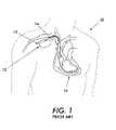
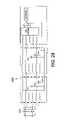
- FIG. 1is a schematic view of an implantable medical device 12 embodying protection against electrical interference. At least one lead 14 is connected to the implantable medical device 12 in connector block region 13 using an interface.
- the pacemaker 12includes at least one or both of pacing and sensing leads represented generally as leads 14 to sense electrical signals attendant to the depolarization and repolarization of the heart 16 , and to provide pacing pulses for causing depolarization of cardiac tissue in the vicinity of the distal ends thereof.
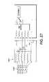
- FIG. 2more particularly illustrates the circuit that is used conventionally to protect from electromagnetic interference.
- protection circuitry 15is provided using a diode array component 30 .
- the diode arrayconsists of five zener diode triggered semiconductor controlled rectifiers (SCRs) with anti-parallel diodes arranged in an array with one common connection. This allows for a small footprint despite the large currents that may be carried through the device during defibrillation, e.g., 10 amps.
- the SCRs 20 – 24turn on and limit the voltage across the device when excessive voltage and current surges occur.
- zener diode triggered SCRsmay be connected to an electrically conductive pin, with each electrically conductive pin being connected to a medical device contact region to be wire bonded to pads of a printed circuit board.
- the diode array component 30 of FIG. 2may be connected to the electrically conductive pins via die contact regions along with other electrical conductive traces of the printed circuit board.
- U.S. Pat No. 5,968,083(to Ciciarelli et al.) describes a device adapted to switch between low and high impedance modes of operation in response to EMI insult.
- U.S. Pat No. 6,188,926(to Vock) discloses a control unit for adjusting a cardiac pacing rate of a pacing unit to an interference backup rate when heart activity cannot be sensed due to EMI.
- Another problem associated with magnetic-resonance imagingis the temperature change in tissue regions caused by using conventional magnetic-resonance imaging techniques.
- a substancesuch as human tissue is subjected to a static magnetic field
- the individual magnetic moments of the spins in the tissuealign in a parallel and anti-parallel direction with the static magnetic field. This direction along the static magnetic field can be termed as the longitudinal direction.
- the radio frequency polarizing field used for spin manipulationis constantly changing and thus, the individual magnetic moments of the spins in the tissue attempt to align with the polarizing field.
- the constant changing of alignment of the magnetic moments of the spins in the tissuecauses the tissue's temperature to increase, thereby exposing the tissue to possible magnetic-resonance imaging induced thermal damage.
- conventional medical assist devicesprovide some means for protection against electromagnetic interference, these conventional medical assist devices require much circuitry and fail to provide fail-safe protection against radiation produced by magnetic-resonance imaging procedures. Moreover, the conventional medical assist devices fail to address the possible damage that can be done at the tissue interface due to radio-frequency-induced heating. Furthermore, the conventional medical assist devices fail to address the unwanted tissue region stimulation that may result from radio-frequency-induced electrical currents. Lastly, conventional magnetic-resonance imaging processes fail to provide a proper safeguard against potential magnetic-resonance imaging induced thermal damage due to the tissue's exposure to the switching magnetic field gradients and the circularly polarized Radio Frequency Field of the magnetic-resonance imaging process.
- a first aspect of the present inventionis directed to a medical assist system.
- the medical assist systemincludes a primary device housing, the primary device housing having a control circuit therein; a lead system to provide an electrical path between a tissue region and the primary device housing; and a shielding formed around the lead system to shield the lead system from electromagnetic interference.
- the shieldingis patterned with non-conductive materials and conductive material.
- a second aspect of the present inventionis directed to a medical assist device.
- the medical assist deviceincludes a primary device housing, the primary device housing having a control circuit therein, and a shielding formed around the primary device housing to shield the primary device housing and any circuits therein from electromagnetic interference.
- the shieldingis patterned with non-conductive materials and conductive material.
- a third aspect of the present inventionis directed to an electromagnetic shielded implantable lead.
- the electromagnetic shielded implantable leadincludes an electrical lead and a shielding formed around the electrical lead to shield the electrical lead from electromagnetic interference.
- the shieldingis patterned with non-conductive materials and conductive material.
- a fourth aspect of the present inventionis directed to an electromagnetic shield.
- the electromagnetic shieldincludes a first patterned layer having non-conductive materials and conductive material and a second patterned layer having non-conductive materials and conductive material.
- a fifth aspect of the present inventionis a magnetic-resonance imaging process.
- the magnetic-resonance imaging processimages a tissue region according to an image acquisition sequence and adjusts the image acquisition sequence, in response to a predetermined parameter, to allow for cooling of the imaged tissue region.
- a sixth aspect of the present inventionis a magnetic-resonance imaging process.
- the magnetic-resonance imaging processimages a tissue region according to an image acquisition sequence; adjusts the image acquisition sequence, in response to a predetermined parameter, to allow for cooling of the imaged tissue region; and shields components of a medical assist device with a shield patterned with non-conductive materials and conductive material.
- a seventh aspect of the present inventionis a device for amplifying an electrical signal of physiological significance in a magnetic-resonance imaging environment.
- the deviceincludes at least two electrodes with associated input leads for coupling to a patient; an amplifier having a zero-signal reference terminal for detecting and amplifying the desired physiological signal; and a filter, connected to the input leads and coupling the at least two electrodes to the amplifier, to attenuate any induced radio-frequency signal produced in the magnetic-resonance imaging environment and passing the lower frequency desired electrical physiological signal.
- the filterincludes a shield enclosing the filter. The shield enclosing the filter is patterned with non-conductive materials and conductive material.
- An eighth aspect of the present inventionis a medical assist system.
- the medical assist deviceincludes a primary device housing; the primary device housing having a control circuit therein; a lead system to provide an electrical path between a tissue region and the primary device housing; a shielding formed around the lead system to shield the lead system from electromagnetic interference; and a filter, connected to the lead system, to attenuate any induced radio-frequency signal and passing a desired electrical physiological signal.
- the filterincludes a shield enclosing the filter and a low pass filter connected to the lead system. The shielding is patterned with non-conductive materials and conductive material.
- a ninth aspect of the present inventionis a medical assist system.
- the medical assist systemincludes a primary device housing, the primary device housing having a control circuit therein; a lead system to provide an electrical path between a tissue region and the primary device housing; and a shielding formed around the lead system to shield the lead system from electromagnetic interference.
- the shieldingis an apertured conductive material having a maximum aperture dimension of 0.01 millimeters to 10 millimeters.
- a tenth aspect of the present inventionis a medical assist device.
- the medical assist deviceincludes a primary device housing, the primary device housing having a control circuit therein; and a shielding formed around the primary device housing to shield the primary device housing and any circuits therein from electromagnetic interference.
- the shieldingis an apertured conductive material having a maximum aperture dimension of 0.01 millimeters to 10 millimeters.
- An eleventh aspect of the present inventionis an electromagnetic shielded lead.
- the electromagnetic shielded leadincludes an electrical lead and a shielding formed around the electrical lead to shield the electrical lead from electromagnetic interference.
- the shieldingis an apertured conductive material having a maximum aperture dimension of 0.01 millimeters to 10 millimeters.
- a twelfth aspect of the present inventionis an electromagnetic shield.
- the electromagnetic shieldincludes a first apertured conductive material having a maximum aperture dimension of 0.01 millimeters to 10 millimeters and a second apertured conductive material having a maximum aperture dimension of 0.01 millimeters to 10 millimeters.
- a further aspect of the present inventionis a magnetic-resonance imaging process.
- the magnetic-resonance imaging processimages a tissue region according to an image acquisition sequence; adjusts the image acquisition sequence, in response to a predetermined parameter, to allow for cooling of the imaged tissue region; and shields components of a medical assist device with a shield being an apertured conductive material and having a maximum aperture dimension of 0.01 millimeters to 10 millimeters.
- a still further aspect of the present inventionis a device for amplifying an electrical signal of physiological significance in a magnetic-resonance imaging environment.
- the deviceincludes at least two electrodes with associated input leads for coupling to a patient; an amplifier having a zero-signal reference terminal for detecting and amplifying the desired physiological signal; and a filter, connected to the input leads and coupling the at least two electrodes to the amplifier, to attenuate any induced RF signal produced in the magnetic-resonance imaging environment and passing the lower frequency desired electrical physiological signal.
- the filterincludes a shield enclosing the filter.
- the shieldis an apertured conductive material having a maximum aperture dimension of 0.01 millimeters to 10 millimeters.
- the medical assist systemincludes a primary device housing, the primary device housing having a control circuit therein; a lead system to provide an electrical path between a tissue region and the primary device housing; a shielding formed around the lead system to shield the lead system from electromagnetic interference; and a filter, connected to the lead system, to attenuate any induced RF signal and passing a desired electrical physiological signal.
- the filterincludes a shield enclosing the filter and a low pass filter connected to the lead system.
- the shieldingis an apertured conductive material having a maximum aperture dimension of 0.01 millimeters to 10 millimeters.
- FIGS. 1 and 2are illustrations of conventional techniques used to protect against electromagnetic interference
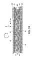
- FIG. 3is a cross-sectional view of one embodiment of segmented shielding of a wire lead according to the concepts of the present invention
- FIG. 4is a cross-sectional view of another embodiment of segmented shielding of a wire lead according to the concepts of the present invention.
- FIG. 5is a top view of a layer of an embodiment of the shielding, having a predetermined segmented pattern of conductive materials, for a wire lead shielding according to the concepts of the present invention
- FIG. 6is a top view of a layer of another embodiment of the shielding, having a predetermined segmented pattern of conductive materials, for a wire lead according to the concepts of the present invention
- FIG. 7is a top view of a layer of another embodiment of the shielding, having a random pattern of conductive materials, for a wire lead according to the concepts of the present invention.
- FIG. 8is a flowchart illustrating the altering of a magnetic-resonance imaging acquisition process in response to a measured temperature of the tissue region being imaged, according to the concepts of the present invention
- FIG. 9is a flowchart illustrating the altering of a magnetic-resonance imaging acquisition process in response to a measured localized specific absorption ratio of the tissue region being imaged, according to the concepts of the present invention.
- FIG. 10is a block diagram of an ECG amplifier capable of operating in the high static magnetic field, radio-frequency field, and gradient field environment produced in a magnetic-resonance imaging system, according to the concepts of the present invention
- FIG. 11is a block diagram of a pacemaker capable of operating in the high static magnetic fields, radio-frequency field, and gradient field environment produced in a magnetic-resonance imaging system, according to the concepts of the present invention
- FIG. 12is a block diagram of an implantable pacemaker, designed for external programming, which operates safely in the environment produced in a magnetic-resonance imaging system, according to the concepts of the present invention
- FIGS. 13 through 18are schematic drawings of various ECG lead and/or harness configurations designed for operation in the environment produced by an magnetic-resonance imaging system, according to the concepts of the present invention
- FIGS. 19 and 20are block diagrams of ECG amplifiers with a one-stage radio-frequency filter design, according to the concepts of the present invention, for use with dual unshielded leads;
- FIGS. 21 and 22are block diagrams of ECG amplifiers with a one-stage radio-frequency filter design, according to the concepts of the present invention, for use with dual shielded leads;
- FIGS. 23 and 24are block diagrams of ECG amplifiers with a multistage radio-frequency filter design, according to the concepts of the present invention, for use with dual unshielded leads;
- FIGS. 25 and 26are block diagrams of ECG amplifiers with a multistage radio-frequency filter design, according to the concepts of the present invention, for use with dual shielded leads;
- FIGS. 27 and 28are block diagrams of ECG amplifiers with a multistage radio-frequency filter design, according to the concepts of the present invention, for use with a multi-lead ECG harness;
- FIG. 29is a block diagram of a magnetic-resonance imaging safe implantable pacemaker in accordance with the present invention.
- FIG. 30is a block diagram of a magnetic-resonance imaging safe implantable pacemaker using a multistage radio-frequency filter, according to the concepts of the present invention.
- FIG. 31is a block diagram of an implantable stimulator capable of operating in a magnetic-resonance imaging system, in accordance with the present invention.
- FIG. 32is a cross-sectional view of one embodiment of an apertured shielding of a wire lead according to the concepts of the present invention.
- FIG. 33is a cross-sectional view of another embodiment of an apertured shielding of a wire lead according to the concepts of the present invention.
- FIG. 34is a top view of a layer of an embodiment of the apertured shielding, having a predetermined apertured pattern of non-conductive materials, for a wire lead shielding according to the concepts of the present invention
- FIG. 35is a top view of a layer of another embodiment of the apertured shielding, having a predetermined apertured pattern of non-conductive materials, for a wire lead according to the concepts of the present invention.
- FIG. 36is a top view of a layer of another embodiment of the apertured shielding, having a random apertured pattern of non-conductive materials, for a wire lead according to the concepts of the present invention.
- the present inventionis directed to an implantable device, such as a medical assist device, that is immune or hardened to electromagnetic insult or interference.
- the term, medical assist device/system or tissue invasive device/systemrefers to any device/system that may enable monitoring of living tissue(s) or living system(s) wherein the monitoring may be, but not limited to an EKG signal, an ECG signal, a glucose level, hormone level, cholesterol level, or magnetic resonance image.
- the medical assist device/system or tissue invasive device/systemmay also enable stimulus intervention to provide assistance to living tissue(s) or living system(s) so that the stimulus causes the selected body tissue or system to function as desired.
- the stimulusmay be, but not limited to, a cardiac stimulating substance or electrical pulse, a blood thinning substance, insulin, estrogen, progesterone, or testosterone.
- the medical assist device/system or tissue invasive device/systemmay also provide therapeutic treatment to the living tissue(s) or living system(s) so that the treatment causes the selected body tissue or system to function as desired.
- the stimulusmay be, but not limited to, radio frequency or laser ablation.
- the medical assist device/system or tissue invasive device/systemmay be implanted in a body cavity of a living organism, either temporarily or permanently, or subcutaneously implanted into a living organism either temporarily or permanently.
- the medical assist device/system or tissue invasive device/systemmay be located external to the living organism.
- Examples of medical assist devices/systems or tissue invasive devices/systemsare, but not limited to, wearable or implantable cardiac pacers (such as pacemakers), implantable pulse generators (IPGs), cardioverter/defibrillator/pacemakers (CDPs), cardiac monitoring systems, insulin pump controllers, brain monitoring systems, cardiac assist devices, implanted insulin pumps, catheter guide wires, leads for neurostimulation probes, intraluminal coils, guided catheters, temporary cardiac pacemakers, temporary esophageal pacemakers, etc.
- cardiac pacerssuch as pacemakers
- IPGsimplantable pulse generators
- CDPscardioverter/defibrillator/pacemakers
- cardiac monitoring systemsinsulin pump controllers
- brain monitoring systemscardiac assist devices
- implanted insulin pumpsimplanted insulin pumps
- catheter guide wiresleads for neurostimulation probes, intraluminal coils, guided catheters, temporary cardiac pacemakers, temporary esophageal pacemakers, etc.
- the conceptsare directed to any medical assist device/system, tissue invasive device/system or tissue interactive device/system which includes electrical components that require shielding from electromagnetic interference or insult such that the interference or insult could cause damage to the electrical components or damage to the surrounding tissue.
- a typical medical devicemay be a pacemaker.
- the pacemakermay include at least one or both of pacing and sensing leads represented generally as leads to sense electrical signals attendant to the depolarization and repolarization of the heart and to provide pacing pulses for causing depolarization of cardiac tissue in the vicinity of the distal ends thereof.
- the pacemaker or cardiac assist devicemay include a primary device housing.
- the primary device housingmay include a control circuit, such as a microprocessor integrated circuit for controlling the operations of the cardiac assist system.
- the control circuitmay select a mode of operation for the cardiac assist system based on predetermined sensed parameters.
- the primary device housingmay also include circuitry to detect and isolate cross talk between device pulsing operations and device sensing operations.
- the control circuitmay isolate physiological signals using a noise filtering circuit or a digital noise filtering.
- the control circuitcan be programmable from a source external of the primary device housing or the control circuit can provide physiological diagnostics to a source external of the primary device housing.
- the primary device housingmay include a power source.
- the power sourcemay be a battery power source in combination with a battery power source measuring circuit.
- the control circuitmay automatically adjust a value for determining an elective replacement indication condition of a battery power source such that the value is automatically adjusted by the control circuit in response to a measured level of a state of the battery power source, the measured level generated by the battery power source measuring circuit connected to the battery power source.
- both the primary housing and the leads of the medical assist device/systemrequire protection or shielding from electromagnetic interference or insult.
- the present inventionprovides a shielding that substantially prevents electromagnetic interference from damaging any, contained therein, electrical components or damage to the tissue surrounding the medical assist device/system's primary housing or leads.
- the shieldingis a compilation of patterned layers having non-conductive materials and conductive materials contained in each patterned layer.
- conductive materialprovides a shield or block for electromagnetic radiation, especially radio frequency radiation (“radio-frequency”) or magnetic radiation (“magnetic-resonance imaging”) used in magnetic-resonance imaging so that the magnetic-resonance imaging radiation cannot penetrate the conductive materials to do damage to any electrical components located on the other side of the shield.
- radio frequency radiationradio frequency
- magnetic-resonance imagingmagnetic radiation
- conductive materialmay provide a block to the magnetic-resonance imaging radiation so as to prevent penetration of the magnetic-resonance imaging radiation
- the blocking of the magnetic-resonance imaging radiationcan cause eddy currents to be induced in the conductive material by the changing magnetic fields in the magnetic-resonance imaging radiation.
- the eddy currentsmay cause heating of the conductive material, thereby heating the enclosed electrical components so as to cause damage or heating the surrounding tissue so as to cause tissue damage.
- the conductive material in the shielding of the present inventionis patterned, apertured, or segmented. More specifically, magnetic-resonance imaging radiation shields generally contain thin layers of conductive cladding sometimes separated by insulators or dielectrics. In the present invention, the conductive material in a layer is patterned, apertured, or segmented so that the conductive material is literally broken up to limit the build up of eddy currents induced by the changing magnetic fields produced during magnetic-resonance imaging.
- FIG. 3An example of such a patterned or segmented shielding for use with an electrical lead is illustrated in FIG. 3 .
- an electrical lead 60is initially coated with an insulation layer 62 so as to electrically insulate the electrical lead from its surroundings.
- a first patterned or segmented layer 80 of shieldingis placed or formed thereon.
- the first patterned or segmented layer 80includes conductive materials 64 and non-conductive material(s) 66 .
- a second patterned or segmented layer 82 of shieldingis placed or formed thereon.
- the second patterned or segmented layer 82includes conductive materials 64 and non-conductive material(s) 66 .
- non-conductive material 66may be formed of a single integral piece of non-conductive material or be formed from a multitude of pieces of non-conductive material, the multitude of pieces being connected together in such a manner to function as a single integral piece of non-conductive material.
- a third patterned or segmented layer 84 of shieldingis placed or formed thereon.
- the third patterned or segmented layer 84includes conductive materials 64 and non-conductive material(s) 66 .
- the conductive materials 64 of this embodiment of the present inventionmay be a metal, a carbon composite, nanotubes (wherein the nanotubes may be constructed from a carbon base or the nanotubes could be formed from other amalgams coated with the appropriate material(s)), metal-coated carbon filaments (wherein the metal may be one of the following metals: nickel, copper, cobalt, silver, gold, tin, or zinc), metal-coated ceramic filaments (wherein the metal may be one of the following metals: nickel, copper, cobalt, silver, gold, tin, or zinc), a composite of metal-coated carbon filaments and a polymer (wherein the polymer may be one of the following: polyether sulfone, silicone, polymide, polyvinylidene fluoride, or epoxy), a composite of metal-coated ceramic filaments and a polymer (wherein the polymer may be one of the following: polyether sulfone, silicone, polymide, polyvinylidene fluoride, or epoxy),
- the non-conductive material(s) 66 of this embodiment of the present inventionmay be a ceramic; glass; mica; anodized copper; metallic oxides; natural or synthetic rubbers; or resins, such as natural resins, epoxy resins, or silicones.
- a biocompatible layer 68may be placed or formed thereon.
- the biocompatible layeris a non-permeable diffusion resistant biocompatible material.
- the conductive materials 64are segmented or patterned in an x-direction, wherein the x-direction is a direction substantially parallel to an axis of the lead 60 . In other words, the conductive materials 64 are broken up in this direction such that one conductive material 64 is physically separated from a neighboring conductive material 64 in the same layer.
- the conductive materials 64 of different layersare segmented or patterned in a y-direction, wherein the y-direction is a direction substantially perpendicular to an axis of the lead 60 .
- the conductive materials 64 of different layersare broken up in this direction such that one conductive material 64 is electrically isolated from a neighboring conductive material 64 in an immediate adjacent layer; i.e., a conductive material 64 in the first patterned or segmented layer 80 is electrically isolated from a neighboring conductive material 64 in the second patterned or segmented layer 82 .
- the x-directional gap between non co-layer immediately x-directional adjacent conductive materials 64is much smaller than the wavelength of the electromagnetic pulse that the shield must attenuate to prevent the incident pulse from passing unattenuated through the shield.
- the conductive materials 64may be segmented or patterned in a z-direction, wherein the z-direction represents the planar surface of a layer as it is wrapped around the lead 60 .
- FIG. 4Another example of such a patterned or segmented shielding for use with an electrical lead is illustrated in FIG. 4 .
- an electrical lead 60is initially coated with an insulation layer 62 so as to electrically insulate the electrical lead from its surroundings.
- a first patterned or segmented layer 80 of shieldingis placed or formed thereon.
- the first patterned or segmented layer 80includes conductive materials 64 and non-conductive material(s) 66 .
- the non-conductive material 66may be formed of a single integral piece of non-conductive material or be formed from a multitude of pieces of non-conductive material, the multitude of pieces being connected together in such a manner to function as a single integral piece of non-conductive material.
- a layer 70 of non-conductive materialis placed or formed thereon.
- a second patterned or segmented layer 82 of shieldingis placed or formed thereon.
- the second patterned or segmented layer 82includes conductive materials 64 and non-conductive material(s) 66 .
- the conductive materials 64 of this embodiment of the present inventionmay be a metal, a carbon composite, nanotubes (wherein the nanotubes may be constructed from a carbon base or the nanotubes could be formed from other amalgams coated with the appropriate material(s)), metal-coated carbon filaments (wherein the metal may be one of the following metals: nickel, copper, cobalt, silver, gold, tin, or zinc), metal-coated ceramic filaments (wherein the metal may be one of the following metals: nickel, copper, cobalt, silver, gold, tin, or zinc), a composite of metal-coated carbon filaments and a polymer (wherein the polymer may be one of the following: polyether sulfone, silicone, polymide, polyvinylidene fluoride, or epoxy), a composite of metal-coated ceramic filaments and a polymer (wherein the polymer may be one of the following: polyether sulfone, silicone, polymide, polyvinylidene fluoride, or epoxy),
- a biocompatible layer 68may be placed or formed thereon.
- the biocompatible layeris a non-permeable diffusion resistant biocompatible material.
- the non-conductive materials 66 of this embodiment of the present inventionmay be a ceramic; glass; mica; anodized copper; metallic oxides; natural or synthetic rubbers; or resins, such as natural resins, epoxy resins, or silicones.
- the conductive materials 64are segmented or patterned in an x-direction, wherein the x-direction is a direction substantially parallel to an axis of the lead 60 . In other words, the conductive materials 64 are broken up in this direction.
- the conductive materials 64are patterned or segmented in a y-direction, wherein the y-direction is a direction substantially perpendicular to an axis of the lead 60 .
- the conductive materials 64are broken up in this direction such that one conductive material 64 is electrically isolated from a neighboring conductive material 64 in an immediate adjacent layer; i.e., a conductive material 64 in the first patterned or segmented layer 80 is electrically isolated from a neighboring conductive material 64 in the second patterned or segmented layer 82 .
- the x-directional gap between non co-layer immediately x-directional adjacent conductive materials 64is much smaller than the wavelength of the electromagnetic pulse that the shield must attenuate to prevent the incident pulse from passing unattenuated through the shield.
- the conductive materials 64may be segmented in a z-direction, wherein the z-direction represents the planar surface of a layer as it is wrapped around the lead 60 .
- the conductive material 64is patterned or segmented to limit the build up of eddy currents. Examples of the patterning of the conductive materials 64 are illustrated in FIGS. 5–7 .
- FIG. 5illustrated a top view of a fabricated layer of the shielding.
- the conductive materials 64are patterned or segmented in such a way that a width of the conductive material 64 in the x-direction, the x-direction being substantially parallel to an axis of a lead, is substantially equal. More specifically, the conductive materials 64 is patterned or segmented in such a way that conductive materials 64 spaced in a predetermined manner, e.g., the spacing between the conductive materials 64 , in the x-direction, may be equal or set in a predetermined manner.
- the spacing between conductive materials 64 in a z-direction, the z-direction representing the planar surface of a layer as it is wrapped around a lead,is not necessarily equal or set in a predetermined manner; however the spacing in the z-direction may be equal or set in a predetermined manner.
- FIG. 6illustrated a top view of a fabricated layer of the shielding.
- the conductive materials 64are patterned or segmented in such a way that a width of the conductive material 64 in the z-direction, the z-direction representing the planar surface of a layer as it is wrapped around a lead, is substantially equal. More specifically, the conductive materials 64 are patterned or segmented in such a way that conductive materials 64 spaced in a predetermined manner; e.g., the spacing between the conductive materials 64 , in the z-direction, may be equal or set in a predetermined manner.
- the spacing between conductive materials 64 in a x-directionis not necessarily equal or set in a predetermined manner; however the spacing in the x-direction may be equal or set in a predetermined manner.
- FIG. 7illustrated a top view of a fabricated layer of the shielding.
- the conductive material 64are patterned or segmented in such a way that the widths of the conductive materials 64 in the z-direction, the z-direction representing the planar surface of a layer as it is wrapped around a lead, are random. More specifically, the conductive materials 64 are patterned or segmented in such a way that conductive materials 64 are spaced in a random manner. Lastly, the spacing between conductive materials 64 in an x-direction, the x-direction being substantially parallel to an axis of a lead, is also random.
- FIGS. 3–7show a shielding with respect to a lead, the shielding can be used to shield other shaped devices such as electrical component housings or other components of a medical assist device/system.
- the actual dimensions of the non-conductive materialscan be set to suppress the radiation and eddy currents induced from specific frequencies; e.g., the lengths of the non-conductive material can be varied to suppress or block specific or undesired radiation frequencies.
- the dimensions of the non-conductive materialwould be on the order of the wavelength of the radiation so as to suppress, block, or shield the radiation.
- the actual layersmay be formed using a photoresist/masking process such as used in integrated circuit fabrication and thin film deposition.
- a photoresist/masking processsuch as used in integrated circuit fabrication and thin film deposition.
- the shieldingmay also be apertured.
- implantable medical devicessuch as pacemaker leads
- body tissuescan be irreversibly damaged by increases in temperature of as little as 2–4° C. Therefore, up to a 50 ⁇ reduction in the amount of energy delivered to the implanted medical device is required to make the device safe, 100 ⁇ if a reasonable design margin of safety is desired. This reduction in the amount of energy delivered to the implanted medical device corresponds to 20 dB of attenuation.
- SE (dB)20 Log [ ⁇ /2 ⁇ r] where ⁇ is the incident wavelength and r is the radius of the circular opening.
- This formulaindicates that a slot or annulus with a greatest dimension equal to 1/20 of the wavelength is required to provide a shielding effectiveness (SE) against heating effects of 20 dB.
- cthe speed of light (3 ⁇ 10 8 meters/second)
- fthe frequency.
- ⁇ m⁇ o /[ ⁇ rel ] 1/2
- ⁇ relthe relative dielectric constant.
- ⁇ ois equal to 4.7 meters
- ⁇ mis equal to 0.5 meters.
- shielding effectivenessis reduced as the number of openings N is increased.
- Shield effectivenessscales as the square root on N.
- Nmay range from 10 to 1000. Therefore, to maintain minimum shield effectiveness against heating effects of 20 dB, the maximum aperture dimension should not exceed approximately 10 millimeters to 1 millimeter, depending upon how many apertures or openings are incorporated into the shield design. At higher frequencies such as 128 MHz (the frequency of emerging MRI facilities), the maximum aperture dimension should not exceed 5 millimeters to 0.5 millimeters.
- implantable medical devicessuch as pacemaker leads
- implantable medical devicesmust also be capable of making sensitive electrical measurements such as intracardiac ECG signals, which are typically 1–25 millivolts.
- a measurement resolution capabilityof less than 0.1 millivolt is required.
- Experimental measurementshave shown that MRI procedures can induce voltages of as much as 100 volts in implanted pacing leads. Therefore, a shield attenuation of 1,000,000 or 60 dB is required, which requires that the maximum aperture dimension must equal 1/2000 of the wavelength.
- FIG. 32An example of such an apertured shielding for use with an electrical lead is illustrated in FIG. 32 .
- an electrical lead 60is initially coated with an insulation layer 62 so as to electrically insulate the electrical lead from its surroundings.
- a first patterned or apertured layer 800 of shieldingis placed or formed thereon.
- the first patterned or apertured layer 800includes conductive material 64 and non-conductive materials 66 .
- a second patterned or apertured layer 820 of shieldingis placed or formed thereon.
- the second patterned or apertured layer 820includes conductive material 64 and non-conductive materials 66 .
- the conductive material 64may be formed of a single integral piece of conductive material or be formed from a multitude of pieces of conductive material, the multitude of pieces being electrically connected together in such a manner to function as a single integral piece of conductive material.
- a third patterned or apertured layer 840 of shieldingis placed or formed thereon.
- the third patterned or apertured layer 840includes conductive material 64 and non-conductive materials 66 .
- the conductive materials 64 of this embodiment of the present inventionmay be a metal, a carbon composite, nanotubes (wherein the nanotubes may be constructed from a carbon base or the nanotubes could be formed from other amalgams coated with the appropriate material(s)), metal-coated carbon filaments (wherein the metal may be one of the following metals: nickel, copper, cobalt, silver, gold, tin, or zinc), metal-coated ceramic filaments (wherein the metal may be one of the following metals: nickel, copper, cobalt, silver, gold, tin, or zinc), a composite of metal-coated carbon filaments and a polymer (wherein the polymer may be one of the following: polyether sulfone, silicone, polymide, polyvinylidene fluoride, or epoxy), a composite of metal-coated ceramic filaments and a polymer (wherein the polymer may be one of the following: polyether sulfone, silicone, polymide, polyvinylidene fluoride, or epoxy),
- the non-conductive materials 66 of this embodiment of the present inventionmay be a ceramic; glass; mica; anodized copper; metallic oxides; natural or synthetic rubbers; or resins, such as natural resins, epoxy resins, or silicones.
- a biocompatible layer 68may be placed or formed thereon.
- the biocompatible layeris a non-permeable diffusion resistant biocompatible material.
- the conductive material 64is patterned or apertured in an x-direction through the utilization of non-conductive materials 66 , wherein the x-direction is a direction substantially parallel to an axis of the lead 60 .
- the conductive material 64is broken up, patterned, or apertured in this direction such that one non-conductive material 66 is physically separated from a neighboring non-conductive material 66 in the same layer.
- the conductive materials 64 of different layersare patterned in a y-direction, wherein the y-direction is a direction substantially perpendicular to an axis of the lead 60 .
- the conductive materials 64 of different layersare broken up in this direction such that one conductive material 64 is electrically isolated from a neighboring conductive material 64 in an immediate adjacent layer; i.e., a conductive material 64 in the first patterned or apertured layer 800 is electrically isolated from a neighboring conductive material 64 in the second patterned or apertured layer 82 .
- the distance of the overlapis much smaller than the wavelength of the electromagnetic pulse that the shield must attenuate to prevent the incident pulse from passing unattenuated through the shield.
- the structure thus formedresembles a waveguide and frequencies well below its cut-off frequency are subject to additional attenuation. For a frequency of 64–128 MHz, this overlap corresponds to approximately 2–3 ⁇ the maximum aperture dimension.
- a minimum shield overlap dimensionshould be 2–3 ⁇ the maximum aperture dimension. It is also important to note that the heating may also increase with increased frequency. At a static magnetic field of 1.5 Tesla the RF transmission frequency is 63.7 MHz, at 3 T it is 127.5 MHz (factor of 42.5 MHz for each Tesla).
- the conductive material 64may be segmented or apertured in a z-direction, wherein the z-direction represents the planar surface of a layer as it is wrapped around the lead 60 .
- FIG. 33Another example of such a shielding for use with an electrical lead is illustrated in FIG. 33 .
- an electrical lead 60is initially coated with an insulation layer 62 so as to electrically insulate the electrical lead from its surroundings.
- a first patterned or apertured layer 800 of shieldingis placed or formed thereon.
- the first patterned or apertured layer 800includes conductive material 64 and non-conductive materials 66 .
- the conductive material 64may be formed of a single integral piece of conductive material or be formed from a multitude of pieces of conductive material, the multitude of pieces being electrically connected together in such a manner to function as a single integral piece of conductive material.
- a layer 70 of non-conductive materialis placed or formed thereon.
- a second patterned or apertured layer 820 of shieldingis placed or formed thereon.
- the second patterned or apertured layer 820includes conductive material 64 and non-conductive materials 66 .
- the conductive materials 64 of this embodiment of the present inventionmay be a metal, a carbon composite, nanotubes (wherein the nanotubes may be constructed from a carbon base or the nanotubes could be formed from other amalgams coated with the appropriate material(s)), metal-coated carbon filaments (wherein the metal may be one of the following metals: nickel, copper, cobalt, silver, gold, tin, or zinc), metal-coated ceramic filaments (wherein the metal may be one of the following metals: nickel, copper, cobalt, silver, gold, tin, or zinc), a composite of metal-coated carbon filaments and a polymer (wherein the polymer may be one of the following: polyether sulfone, silicone, polymide, polyvinylidene fluoride, or epoxy), a composite of metal-coated ceramic filaments and a polymer (wherein the polymer may be one of the following: polyether sulfone, silicone, polymide, polyvinylidene fluoride, or epoxy),
- a biocompatible layer 68may be placed or formed thereon.
- the biocompatible layeris a non-permeable diffusion resistant biocompatible material.
- the non-conductive materials 66 of this embodiment of the present inventionmay be a ceramic; glass; mica; anodized copper; metallic oxides; natural or synthetic rubbers; or resins, such as natural resins, epoxy resins, or silicones.
- the conductive materials 64are patterned or apertured in an x-direction, wherein the x-direction is a direction substantially parallel to an axis of the lead 60 .
- the conductive materials 64are broken up, patterned, or apertured in this direction such that the non-conductive materials 66 break up the conductive material 64 .
- the conductive materials 64are patterned in a y-direction, wherein the y-direction is a direction substantially perpendicular to an axis of the lead 60 .
- the conductive materials 64are broken up in this direction such that one conductive material 64 is electrically isolated from a neighboring conductive material 64 in an immediate adjacent layer; i.e., a conductive material 64 in the first patterned or apertured layer 800 is electrically isolated from a neighboring conductive material 64 in the second patterned or apertured layer 820 .
- the distance of the overlapis much smaller than the wavelength of the electromagnetic pulse that the shield must attenuate to prevent the incident pulse from passing unattenuated through the shield.
- the structure thus formedresembles a waveguide and frequencies well below its cut-off frequency are subject to additional attenuation. For a frequency of 64–128 MHz, this overlap corresponds to approximately 2–3 ⁇ the maximum aperture dimension.
- a minimum shield overlap dimensionshould be 2–3 ⁇ the maximum aperture dimension.
- the conductive materials 64may be segmented in a z-direction, wherein the z-direction represents the planar surface of a layer as it is wrapped around the lead 60 .
- the conductive material 64is patterned or apertured to limit the build up of eddy currents. Examples of the patterning or aperturing of the conductive material 64 are illustrated in FIGS. 34–36 .
- FIG. 34illustrated a top view of a fabricated layer of the shielding.
- the conductive material 64is patterned or apertured in such a way that a width of the conductive material 64 in the x-direction, the x-direction being substantially parallel to an axis of a lead, is substantially equal. More specifically, the conductive material 64 is patterned or apertured in such a way that non-conductive materials 66 spaced in a predetermined manner; e.g., the spacing between the non-conductive materials 66 , in the x-direction, may be equal or set in a predetermined manner.
- the spacing between non-conductive materials 66 in a z-direction, the z-direction representing the planar surface of a layer as it is wrapped around a lead,is not necessarily equal or set in a predetermined manner; however the spacing in the z-direction may be equal or set in a predetermined manner.
- the distance of the overlapis much smaller than the wavelength of the electromagnetic pulse that the shield must attenuate to prevent the incident pulse from passing unattenuated through the shield.
- the structure thus formedresembles a waveguide and frequencies well below its cut-off frequency are subject to additional attenuation. For a frequency of 64–128 MHz, this overlap corresponds to approximately 2–3 ⁇ the maximum aperture dimension.
- a minimum shield overlap dimensionshould be 2–3 ⁇ the maximum aperture dimension.
- FIG. 35illustrated a top view of a fabricated layer of the shielding.
- the conductive material 64is patterned or apertured in such a way that a width of the conductive material 64 in the z-direction, the z-direction representing the planar surface of a layer as it is wrapped around a lead, is substantially equal. More specifically, the conductive material 64 is patterned or apertured in such a way that non-conductive materials 66 spaced in a predetermined manner; e.g., the spacing between the non-conductive materials 66 , in the z-direction, may be equal or set in a predetermined manner.
- the spacing between non-conductive materials 66 in a x-directionis not necessarily equal or set in a predetermined manner; however the spacing in the x-direction may be equal or set in a predetermined manner.
- the distance of the overlapis much smaller than the wavelength of the electromagnetic pulse that the shield must attenuate to prevent the incident pulse from passing unattenuated through the shield.
- the structure thus formedresembles a waveguide and frequencies well below its cut-off frequency are subject to additional attenuation. For a frequency of 64–128 MHz, this overlap corresponds to approximately 2–3 ⁇ the maximum aperture dimension.
- a minimum shield overlap dimensionshould be 2–3 ⁇ the maximum aperture dimension.
- FIG. 36illustrated a top view of a fabricated layer of the shielding.
- the conductive material 64is patterned or apertured in such a way that the widths of the non-conductive materials 66 in the z-direction, the z-direction representing the planar surface of a layer as it is wrapped around a lead, are random. More specifically, the conductive materials 64 are patterned or apertured in such a way that non-conductive materials 66 spaced in a random manner. Lastly, the spacing between non-conductive materials 66 in an x-direction, the x-direction being substantially parallel to an axis of a lead, is also random.
- FIGS. 32–36show a patterned or apertured shielding with respect to a lead, the patterned or apertured shielding can be used to shield other shaped devices such as electrical component housings or other components of a medical assist device/system.
- the actual dimensions of the non-conductive materialscan be set to suppress the radiation and eddy currents induced from specific frequencies; e.g., the lengths of the non-conductive material can be varied to suppress or block specific or undesired radiation frequencies.
- the dimensions of the non-conductive materialwould be on the order of the wavelength of the radiation so as to suppress, block, or shield the radiation.
- the distance of the overlapis much smaller than the wavelength of the electromagnetic pulse that the shield must attenuate to prevent the incident pulse from passing unattenuated through the shield.
- the actual layersmay be formed using a photoresist/masking process such as used in integrated circuit fabrication and thin film deposition.
- a photoresist/masking processsuch as used in integrated circuit fabrication and thin film deposition.
- eddy currents in a conductive structuremay cause heating to the surrounding tissue
- eddy currents induced in the tissuemay also cause the heating of the surrounding tissue.
- the individual magnetic moments of the spins in the tissuealign in a parallel and anti-parallel direction with the static magnetic field. This direction along the static magnetic field can be termed as the longitudinal direction.
- the radio frequency polarizing field used for spin manipulationis constantly changing and thus, the individual magnetic moments of the spins in the tissue attempt to align with the polarizing field.
- the heat being accumulated in the surrounding tissueis addressed and reduced or prevented, notwithstanding the source or cause of the excessive heat.
- the term, specific absorption ratiowill be used in discussing the excessive heat.
- the specific absorption ratiois defined as the amount of power absorbed by a sample within a magnetic-resonance imaging scanner.
- the samplecould be a suitable phantom mimicking tissue properties or a tissue region of patient.
- this excessive heatcould be caused by either eddy currents induced in conductive structures or eddy currents induced in the actual tissue. It is noted that although two distinct sources of excessive heat are identified for the purposes of describing this embodiment of the present invention, the actual source of the heat may not be known, nor is it a real consideration in the actual functionality of this embodiment of the present invention.
- cardiac assist device leadsmetallic guidewires, neurostimulator leads and intraluminal coil leads may induce a localized increase in the specific absorption ratio, thereby resulting in an increased heating of the surrounding tissue.
- the acquisition sequence of the magnetic-resonance imaging processmay also induce a localized increase in the specific absorption ratio, thereby resulting in an increased heating of the surrounding tissue.
- This tissue heatingnotwithstanding the source, may be a function of the time of radio-frequency excitation, gradient coil switching speed, or strength of the static magnetic field.
- the localized specific absorption ratio of tissueis reduced by altering the actual magnetic-resonance imaging acquisition process. More specifically, according to a preferred embodiment of the present invention, the localized specific absorption ratio of tissue is reduced by varying the imaging pulse sequence and/or changing the timing parameters of magnetic-resonance imaging acquisition process. For example, in response to increases in the localized specific absorption ratio or during magnetic-resonance image acquisition, the radio-frequency excitation cycle may be interrupted to allow for cooling of the tissue. In other words, if a threshold temperature level or a localized specific absorption ratio is exceeded, the magnetic-resonance imaging acquisition can be halted until the tissue temperature or localized specific absorption ratio decreases to an accepted level.
- the increased in the localized specific absorption ratiomay or may not have resulted from placement of a conductive structure near the tissue region.
- FIG. 8illustrates a magnetic-resonance imaging process according to the concepts of the present invention, which alters the actual magnetic-resonance imaging acquisition process in response to a temperature change in the tissue region being imaged.
- an image acquisition sequenceis started by the magnetic-resonance imaging system.
- the temperature change in the tissue region being imagedis measured. It is noted that this temperature change may be relative or absolute. The temperature change in the tissue region being imaged can be measured a number of ways.
- the relative temperature changecan be monitored by magnetic image acquisition techniques. More specifically, relative temperature changes can be measured using a double gradient echo sequence to acquire a baseline phase image and a second phase image at within a single radio-frequency excitation of one same pulse sequence. A relative spatial temperature map of the desired region of interest can be calculated based on the subtraction of the two phase images collected during the double gradient echo sequence acquisition.
- absolute temperature changescan be determined using known methods, such as fiber optic thermocouples attached to guidewires or catheters, or non-contact thermographic imaging techniques.
- a predetermined upper temperature thresholdis compared with the calculated temperature change, or in the example described above, compared with the relative temperature map. If the temperature change exceeds or is equal to the predetermined upper temperature threshold, the imaging acquisition sequence is adjusted or halted so as to reduce the temperature change below the predetermined upper temperature threshold, at Step S 4 .
- Step S 5determines if the measured temperature change is above a predetermined lower temperature threshold. If Step S 5 determines that the measured temperature change is above a predetermined lower temperature threshold, the process returns to Step S 4 and the imaging acquisition sequence remains adjusted or halted so as to reduce the temperature of the tissue region of interest. On the other hand, if Step S 5 determines that the measured temperature change is below or is equal to a predetermined lower temperature threshold, the process resume image acquisition at to Step S 6 .
- pulse sequence design and pulse sequence parameter determinationcan be applied to any form of pulse sequence or imaging acquisition method so as it meets the requirements of the user.
- pulse sequence design and pulse sequence parameter determinationThere are an infinite number of variations in pulse sequence design and pulse sequence parameter determination to minimize heating.
- the actual variation in pulse sequence design and pulse sequence parameter determinationwill be dependent upon the image quality and the temporal resolution of acquisition desired; however, the required tissue temperature threshold(s) will be the ultimate determinant.
- This embodimentmay also include a user interactive process, which can be programmed.
- a user interactive processwhich can be programmed.
- An example of such a processis described in detail in U.S. Pat. No. 6,396,266, entitled “magnetic-resonance Imaging System With Interactive magnetic-resonance Geometry Prescription Control.” The entire contents of U.S. Pat. No. 6,396,266 are hereby incorporated by reference.
- the SAR coefficients of a wide range of implantable medical devicesare programmed into the magnetic-resonance imaging system, which then uses these data to predetermine and apply as safe magnetic-resonance imaging sequence.
- a magnetic-resonance imaging processalters the actual magnetic-resonance imaging acquisition process in response to a calculated specific absorption ratio of the tissue region being imaged.
- an image acquisition sequenceis started by the magnetic-resonance imaging system.
- the specific absorption ratiois estimated using theoretical modeling and/or empirical results from certain conductors being imaged in tissues.
- the calculated specific absorption ratio level(s)are then be compared to threshold levels.
- the imaging acquisition sequenceis adjusted or halted so as to reduce the temperature of the tissue region of interest, at Step S 4 .
- Step S 51determines if the determined specific absorption ratio level is above a predetermined lower specific absorption ratio threshold. If Step S 51 determines that the determined specific absorption ratio level is above a predetermined lower specific absorption ratio threshold, the process returns to Step S 4 and the imaging acquisition sequence remains adjusted or halted so as to reduce the temperature of the tissue region of interest. On the other hand, if Step S 51 determines that the determined specific absorption ratio level is below or is equal to a predetermined lower specific absorption ratio threshold, the process resume image acquisition at to Step S 6 .
- This embodimentmay also include a user interactive process described above.
- specific absorption ratio or energy deposition of radio frequency energy in the tissuecan be reduced by specific manipulations of each individual radio frequency pulse.
- these embodiments of the present inventionmay manipulate the pulse waveform, pulse duration and pulse amplitude to reduce the specific absorption ratio.
- the choice of the integrated values of these three parametersis determined upon by the requirements of the user. For example, reduction of the amplitude and increase in the duration of the pulse may reduce the specific absorption ratio, but this may not be appropriate for the specified timing required to image certain contrast parameters.
- FIGS. 8 and 9can be used not only as a stand-alone solution to reduce the increases in specific absorption ratio resulting from conductive structures in tissue, but also in conjunction with the patterned shielding embodiments described above.
- FIG. 10A block diagram of an ECG acquisition and processing system is shown in FIG. 10 .
- the ECG monitoring systemcan be used as a stand-alone ECG monitor or as part of an external or internal pacemaker.
- a patientis connected to ECG monitoring circuitry 110 via surface or internal electrodes 112 and lead wires 114 .
- the lead wires 114connect to the input ECG/radio-frequency filter 116 .
- the radio-frequency filterprevents the development of excess voltage on the ECG input amplifier and processor 118 that would otherwise damage the amplifier, and excess voltage on the ECG leads potentially inducing a dangerous heart rhythm. Second, it prevents the development of excess current on the ECG electrodes 112 that would induce thermogenic damage at the electrode-heart tissue interface that could lead to loss of capture of pacing signals and possibly death. Third, the radio-frequency filter 116 , when attached between the lead wires 114 and the ECG input amplifier, will not interfere with proper sensing of the ECG signal.
- the input ECG/radio-frequency filter 116has the characteristics of a low-pass filter with approximately 100 dB signal attenuation in the commonly used magnetic-resonance imaging system radio-frequency frequency range. The frequencies contained in the intracardiac or surface ECG signal, however, are passed without any attenuation.
- inductors 120may be placed in the lead wires 114 , close to the electrodes.
- the ECG/radio-frequency input filter 116 and lead wire inductors 120must contain components with a resonance frequency higher than the radio-frequency frequency of the magnetic-resonance imaging system in use.
- the ECG amplifier/processor 118contains low-pass or band reject filter 119 placed after the initial amplifier 117 and before final stages 121 .
- the low-pass or band reject filtermust pass the QRS signals and reject gradient field and radio-frequency frequencies.
- the output ECG signal 122which can take any conventional form such as an R-wave detector output or analog ECG, can be used for any purpose. It can be used to display the ECG on monitor 124 , or synchronize an external or internal device 126 , such as a magnetic-resonance imaging system or cardiac pacemaker.
- a pacemaker system 128is described.
- This pacemaker systemcan be either external or implantable.
- this embodimentalso contains a pacing output stage 130 that is controlled by the pacing logic 132 .
- the pacing logicis itself controlled by signals from the ECG amplifier/processor 134 .
- the patientis connected to the pacemaker system 128 , via surface or internal sensing electrodes 136 and lead wires 138 .
- the lead wiresare connected to the ECG amplifier/processor 134 , via the input ECG/radio-frequency filter 140 .
- the pacing output stage 130is connected to pacing electrodes 142 via the output radio-frequency filter 144 and pacing lead wires 146 .
- the ECG amplifier/processor 134contains a low-pass or band reject filter 135 placed after the initial amplifier 133 and before the final stages 137 .
- the low-pass or band reject filtermust pass the QRS signal and reject gradient field frequencies caused by the magnetic-resonance imaging.
- inductors 148 , 150may be placed in the lead wires 138 , 146 close to the electrodes 136 , 142 .
- the sensing 136 and pacing 142 electrodes, wires 138 , 146 , inductors 148 , 150 , and radio-frequency filters 149 , 144are shown separately. However, these components can be merged to create a combined ECG sensing/pacing radio-frequency electrodes, wires, inductors, and filters.
- the implantable pacemaker 150capable of bi-directional communication with an external programmer 152 is shown in FIG. 12 .
- the implantable unitcontains conventional programmable pacing logic 154 for sensing and/or pacing the ventricle and/or atrium and includes an ECG amplifier and processor 156 , pacing output stage 158 , combined input/output radio-frequency filter 160 , electrodes 162 and leads 164 .
- the ECG amplifier and processor 156contains a low-pass or band reject filter 157 placed after the initial amplifier 155 and before final stages 159 .
- the low-pass or band reject filtermust pass the QRS signals and reject gradient field frequencies caused by the magnetic-resonance imaging.
- inductors 166may be placed in the lead wires 164 close to the electrodes 162 .
- the electrodes 162 , leads 164 , inductors 166 , and input/output filter 160may be single elements performing combined input and output functions or may be separate input and output elements.
- multiple sets of sensing/pacing electrodesmay be used 159 , 162 , which are each connected to input/output radio-frequency filters 160 .
- a first electrode pairmay be for atrium sensing or pacing and a second electrode pair may be for ventricle sensing or pacing.
- pacing logic 154may be programmed, for example, to sense the atrium signal and pace via the ventricle electrodes.
- a new form of circulatory support called cardiomyoplastymay utilize other electrodes 161 and leads 167 to pace skeletal muscle wrapped around the heart and stimulated in synchrony with pacing the heart.
- the leads 163 , 164 , 167may contain inductors 165 , 166 , 169 to reduce electrical currents across the electrodes and each lead may be connected to separate input/output radio-frequency filter 160 .
- this shieldis as described above with respect to FIGS. 3 through 7 .
- the shieldmay consist of patterned layers including conductive materials and non-conductive materials.
- the conductive materials of the present inventionmay be a metal, a carbon composite, nanotubes (wherein the nanotubes may be constructed from a carbon base or the nanotubes could be formed from other amalgams coated with the appropriate material(s)), metal-coated carbon filaments (wherein the metal may be one of the following metals: nickel, copper, cobalt, silver, gold, tin, or zinc), metal-coated ceramic filaments (wherein the metal may be one of the following metals: nickel, copper, cobalt, silver, gold, tin, or zinc), a composite of metal-coated carbon filaments and a polymer (wherein the polymer may be one of the following: polyether sulfone, silicone, polymide, polyvinylidene fluoride, or epoxy), a composite of metal-coated ceramic filaments and a polymer (wherein the polymer may be one of the following: polyether sulfone, silicone, poly
- the implantable pacemaker shown in FIG. 12Since the implantable pacemaker shown in FIG. 12 is enclosed in a radio-frequency shield, it was necessary to develop a unique method of external programming.
- the information received by the pacemaker 150is processed to separate the desired communication signal from the radio-frequency signals produced by the magnetic-resonance imaging system.
- An antenna 170is connected to the telemetry radio-frequency amplifier 172 via the telemetry receiver/band pass filter 174 .
- This filteris a band pass filter that passes only the specific programming frequency to the telemetry amplifier 172 .
- the telemetry logic circuit 176interprets all radio-frequency received by the telemetry antenna 170 and will only allow programming of the pacing logic circuit 154 when a specific telemetry enable pattern is received.
- the telemetry enable logic circuit 176will also inhibit control of the pacing output stage 158 while programming is taking place. This prevents improper and potentially dangerous pacing parameters from controlling the pacing stage.
- the telemetry enable circuit 176enables pacing at a preset rate (“safety pacing”) to provide adequate pacing back-up for pacemaker dependent patients during external programming.
- FIGS. 13 through 18are schematic diagrams of the inductor elements (elements 120 , 148 , 150 , 165 , 166 , and 169 ) that are placed in the lead wires to reduce harmful currents.
- significant stray capacitancecan be produced along the lead wires, particularly for external pacers. As a result,
- FIGS. 13 through 18Electromagnetic fields generated between the electrodes because of the radio-frequency field can produce dangerously high voltages across and currents flowing through the electrodes.
- FIGS. 13 through 18are placed in the lead wires close to the electrodes.
- FIG. 13shows the inductor elements 178 when a two-wire lead is used.
- FIG. 14shows the inductor elements 180 when a two-wire shielded lead is used.
- FIG. 15shows alternative inductor elements 182 , which incorporate a capacitor 184 , thus comprising an additional low-pass L-C filter.
- FIG. 16shows the same alternative inductor elements 183 and a capacitor 185 , as shown in FIG. 15 , but using a shielded two-wire lead.
- FIG. 13shows the inductor elements 178 when a two-wire lead is used.
- FIG. 14shows the inductor elements 180 when a two-wire shielded lead is used.
- FIG. 15shows alternative inductor elements 182 , which incorporate
- FIG. 17shows the inductor elements 186 used in a multi-lead shielded harness.
- FIG. 18shows alternative inductor elements 188 used in a multi-lead shielded harness, which also includes capacitor components 190 connected to the shielding enclosure of the capacitors.
- the leadscan be used to measure ECG, EEG, or other electrical signals of physiological significance.
- FIG. 13 through 18show twisted leads, but it is to be understood that coaxial as well as other forms of lead wires could be used.
- FIGS. 19 through 31show various embodiments of the input radio-frequency filter, output radio-frequency filter, and combined input/output radio-frequency filter. According to the concepts of the present invention, there are many possible specific implementations of the radio-frequency filter design that will depend on: 1) whether two leads or multiple leads are used; 2) whether the leads are shielded; 3) whether single or multiple stage filtering is used; and 4) whether each radio-frequency filter is housed in a separate shielded enclosure.
- the filterscould be placed either at the proximal end or the distal end of the pulse generator—lead assembly.
- the same filter design principlescan be used whether the filter is acting as an input filter for an ECG monitor, as separate input filters and output filters for a pacemaker, or as a single combined input/output filter for a pacemaker.
- FIGS. 19 and 20show one-stage filters for use with two unshielded leads.
- FIGS. 21 and 22show alternative ways to shield the electronics.
- FIG. 19shows the input filter 192 in a separate shielded enclosure; whereas FIG. 20 shows the input filter 196 located in the same-shielded enclosure 198 as the processing electronics 1100 with an internal wall 1102 shielding the monitoring electronics 1100 from the input filter 196 . (Whether one or two enclosures are used, the filter section should be shielded from the other circuitry.)
- each leadis connected to a separate low-pass filter.
- Leads 1103may be twisted to reduce electromagnetic interference.
- a first low-pass filteris made from inductor 1104 and capacitor 1106 ; and a second low-pass filter is made from inductor 1108 and capacitor 1110 .
- Each low-pass filteroffers approximately 100 dB signal attenuation in the radio-frequency frequency range of the magnetic-resonance imaging system and passes with little attenuation the desired physiological signal.
- the L-C componentsmust be high frequency elements retaining their desired characteristics throughout the frequency range.
- the output from the input filter 192is connected to differential amplifier 1112 .
- the non-inverting input of the ECG amplifier 1112is connected to the amplifier zero-signal reference terminal via a resistor 1114 , as is well known in the art.
- any other method of converting a two to three conductor inputmay also be used.
- the two capacitors 1106 , 1110 in the low-pass filtersare referenced to a third wire 1116 that is connected to the shield surrounding the filter 1122 and also connected to the zero-signal reference terminal of the ECG amplifier 1112 .
- the ECG amplifiermay be a single differential amplifier or a combination of multiple differential amplifiers.
- capacitors 1106 , 1110can be connected directly to the shield 1122 with a separate wire connecting the shield 1122 to the zero-signal reference terminal of the ECG amplifier 1112 .
- resistors 1118 , 1120may be added between the input filter 192 and the input of the differential amplifier 1112 .
- the ECG amplifier 1112 and processor 1124may also be enclosed in a separate shield 1125 .
- the shieldsmay consist of patterned layers including conductive materials and non-conductive materials.
- the conductive materials of the present inventionmay be a metal, a carbon composite, nanotubes (wherein the nanotubes may be constructed from a carbon base or the nanotubes could be formed from other amalgams coated with the appropriate material(s)), metal-coated carbon filaments (wherein the metal may be one of the following metals: nickel, copper, cobalt, silver, gold, tin, or zinc), metal-coated ceramic filaments (wherein the metal may be one of the following metals: nickel, copper, cobalt, silver, gold, tin, or zinc), a composite of metal-coated carbon filaments and a polymer (wherein the polymer may be one of the following: polyether sulfone, silicone, polymide, polyvinylidene fluoride, or epoxy), a composite of metal-coated ceramic filaments and a polymer (wherein the polymer may be one of the following: polyether sulfone, silicone,
- FIG. 20shows an alternative embodiment where the input filter 196 and processing electronics 1100 are housed in a single contiguous shielding enclosure 198 .
- a separate metallic wall 1102is used to shield the electronics 1100 from the input filter 196 .
- the two capacitors 1126 , 1128 that make up the low-pass filtersare connected to the zero-signal reference terminal of the differential amplifiers 1130 via a third reference wire 1132 ; the reference wire 1132 and zero-signal reference terminal 1134 both connected to the pacemaker shielding case at a single point.
- FIGS. 19 and 20show processing electronics 1224 , 1136 that are used to further process the signal obtained from the differential amplifiers 1112 , 1130 .
- the processing electronicsmay be used to process and display the ECG signal, in the case of an external monitor, or be used to process and control pacing in the case of a pacemaker. It is to be understood that the filter embodiments shown in FIGS. 19 and 20 could be used in a device that monitors physiologically significant electrical signals other than ECG.
- FIGS. 21 and 22show one-stage filter designs 1135 and 1137 that is preferred when the input leads are shielded.
- the designis identical to that shown in FIGS. 19 and 20 , except that the lead shield must be coupled to the shield enclosure via a radio-frequency filter.
- the lead shield 1140 of the leads 1138in FIG. 21 , is connected by an inductor 1146 to the third reference wire 1148 , and the reference wire is connected to the filter's shielding enclosure 1150 .
- the shield 1144 of the leads 1142 in FIG. 22is connected by an inductor 1154 to the reference wire 1156 , connected in turn to the enclosure 1160 .
- more than one stage of filteringcan be used.
- Each filter stageis similar to the filter described in FIG. 19 .
- Each input leadis connected to a low-pass filter.
- Each low-pass L-C filterhas a capacitor connected to a reference wire that is connected to the shielding enclosure.
- the first stage filter 1162contains low-pass filters comprising inductors 1164 , 1166 and capacitors 1168 , 1170 . Capacitors 1168 , 1170 are coupled to a reference wire 1172 that is connected to the enclosure 1174 .
- the second filter stage 1176contains low-pass filters made from inductors 1178 , 1180 and capacitors 1182 , 1184 , with capacitors 1182 , 1184 coupled to the reference wire 1172 that is connected to the shielding enclosure 1177 . All the capacitors ( 1168 , 1170 , 1182 and 1184 ) used in the low-pass filters are connected to the reference wire 1172 which is connected to the zero-signal reference terminal of the differential amplifier 1188 .
- Each stage in FIG. 23is housed in a separate shielding enclosure and each shielding enclosure is coupled to the reference wire 1172 . It is understood that this concept can be extended to multistage filtering.
- the second stage 1176could actually represent the Nth stage of a multistage filter, with each identical stage coupled together as shown.
- FIG. 24An alternative embodiment for multiple stage filtering is shown in FIG. 24 .
- each filtering stage as well as the differential amplifier and the associated electronicsare housed in the same contiguous shielding enclosure 1192 .
- the filter design in this embodimentis identical to that shown in FIG. 20 ; however, the reference wire is only connected to the shielding case 1192 at a single point.
- the low-pass filters in each stage and the zero-signal reference terminal of the differential amplifier 1194are all referred to the same point on the shielding enclosure.
- the embodiment shown in FIG. 24may also have three or more stages, each stage shielded and coupled together as shown.
- FIGS. 25 and 25are schematic drawings of a two-stage filter for use with shielded leads. These filters are similar to the multistage filter embodiments shown in FIGS. 23 and 24 , except that the lead shields are coupled via inductors to the reference wire in the last filter stage.
- FIG. 25is a two-stage filter where each stage is separately isolated in enclosures 1196 , 1198 . Again, as in the previous embodiments, low-pass filters are connected in each input lead and referenced to a common reference line 1200 (i.e., capacitors 1202 , 1204 , 1206 , and 1208 are connected to the reference line 1200 ). The common reference line 1200 is connected to the shielding enclosure for each stage and is input to the zero-signal reference terminal of the differential amplifier 1210 .
- the lead shield 1212is connected to inductor 1214 in the first filter stage and via line 1215 to inductor 1216 in the second filter stage.
- the inductor 1216 in the second, or final filter stageis connected to the common reference line 1290 .
- the inductors 1214 , 1216provide high impedance to the undesirable high frequency radio-frequency voltages produced by the magnetic-resonance imaging system and prevent introduction of radio-frequency interference into the processing electronics via the common wire.
- an additional capacitor 1218may be connected between lines 1215 and 1200 in the first stage and any subsequent filter stage other than the last stage.
- Inductor 1214coupled with capacitor 1218 , provides a third low-pass filter.
- FIG. 26is a multistage filter housed in a single shielding enclosure 1220 with separate walls 1222 , 1224 isolating the filtering stages from each other and from the processing electronics.
- each lead 1228 and the lead shield 1230are coupled to low-pass filters referenced by capacitors 1230 , 1232 , and 1234 to a common reference line 1236 .
- the last stage 1238only the two lead wires contain low-pass filters referenced by capacitors 1240 , 1242 to the common reference line 1236 .
- the lead shield 1230is coupled via inductor 1244 directly to the reference line 1236 .
- the reference line 1236is connected to the zero-signal reference terminal of the differential amplifier 1248 . Also as in the other embodiments, when a single case is used, the common reference line 1236 is connected to the shielding enclosure at a single point. It is of course understood that the two-stage filters shown in FIGS. 25 and 26 could be easily extended to multiple stage filtering with each stage connected as described.
- FIGS. 27 and 28show an extension of the single and multiple stage filtering to multiple lead shielded ECG harness.
- a five conductor shielded cable 1250is filtered by a single stage filter 1252 .
- a five conductor shielded cable 1254is filtered by a multiple stage filter 1256 .
- the filtershave been described as input filters. However, as shown in FIG. 29 , the filters can operate as both input and output filters.
- the lead pair 1258can be used to sense electrical activity of the heart as well as to pace the heart.
- low pass filtersi.e., inductor 1260 /capacitor 1262 pair and inductor 1264 /capacitor 1266 pair
- the reference line 1268then connects to the zero-signal reference terminal of the differential amplifier and to the shielding enclosure.
- a pacing amplifier 1270in controlled by electronics 1272 to generate a pacing signal.
- the pacing signalis connected via lines 1274 , 1276 through the filter, to the leads 1258 .
- Two inductors 1278 , 1280are placed in lines 1274 , 1276 to further prevent any current generated by the magnetic-resonance imaging system from affecting the pacing amplifier 1270 ; the inductors 1278 , 1 provide an additional high impedance to the high frequency radio-frequency signals produced by the magnetic-resonance imaging system.
- Connecting the pacing amplifier to the leads 1258 via the filtercan be used with each of the filter embodiments described above.
- pacing amplifierswould be preferably connected into the last filtering stage.
- FIG. 30is an exemplary embodiment, showing how the pacing amplifier 1282 can be connected via a multi-stage filter to the shielded pacing/sensing leads 1234 .
- the pacing amplifier 1282is connected via inductors 1286 and 1288 to the lead wires in the last stage of the filter. As discussed above, the inductors 1286 , 1288 provide additional protection from the high frequency radio-frequency signals generated by the magnetic-resonance imaging system.
- the filters described hereincan be connected to both sensing electronic and pacing amplifiers.
- the same filter designcan be used in stimulators, as shown in FIG. 31 , where only a pacing signal is produced.
- the filter designis identical to those described previously.
- the leads 1290are each connected to low pass filters (inductor 1291 /capacitor 1292 pair and inductor 1293 /capacitor 1294 pair) that are referred by capacitors 1292 , 1294 to a common reference line 1296 .
- Inductors 1298 , 1300provide additional isolation to protect the pacing amplifier.
- the filter design for stimulation use onlycan be extended to multistage embodiments as described above.
- the conductive materials of the present inventionmay be a metal, a carbon composite, nanotubes (wherein the nanotubes may be constructed from a carbon base or the nanotubes could be formed from other amalgams coated with the appropriate material(s)), metal-coated carbon filaments (wherein the metal may be one of the following metals: nickel, copper, cobalt, silver, gold, tin, or zinc), metal-coated ceramic filaments (wherein the metal may be one of the following metals: nickel, copper, cobalt, silver, gold, tin, or zinc), a composite of metal-coated carbon filaments and a polymer (wherein the polymer may be one of the following: polyether sulfone, silicone, polymide, polyvinylidene fluoride, or epoxy), a composite of metal-coated ceramic filaments and a polymer (wherein the polymer may be one of the following: polyether sulfone, silicone, polymide, polyvinylidene fluoride, or epoxy), a composite of
- a common reference linewas described in the context of a unipolar lead system. It is noted that the common reference line may not be a separate line, but the common reference line may be one of the leads in a bipolar lead system. Moreover, the common reference line may a type of ground path (or line) or signal return path (or line). The common reference line merely provides electrical ground for the filters.
- the present inventionis an electromagnetic shield having a first patterned layer having non-conductive materials and conductive materials and a second patterned layer having non-conductive materials and conductive materials.
- the conductive materials in the first patterned layermay be randomly located or located in a predetermined segmented pattern.
- the conductive materials in the first patterned layermay be located in a predetermined segmented pattern with respect to locations of the conductive materials in the second patterned layer.
- the electromagnetic shieldmay further include a non-conductive layer between the first and second patterned layers such that the conductive materials in the first patterned layer can overlap the conductive materials in the second patterned layer with respect to a direction substantially perpendicular to a planar surface of the second patterned layer.
- the present inventionprovides a patterned shielding that substantially prevents undesired radiation from entering the lead from the radial direction or electrical component and also substantially prevents the formation or inducement of eddy currents on the surface of the shielding, which are induced by the pulsing of the radiation or changing magnetic field of the radiation. More specifically, the conductive material in a shielding layers of the present invention is patterned or segmented so that the conductive material is literally broken up to limit the build up of eddy currents induced by the changing magnetic fields.
- the present inventioncan reduce specific absorption ratio by altering the magnetic-resonance imaging acquisition process by altering the imaging pulse sequence and/or changing the timing parameters.
- the radio-frequency excitation cyclemay be interrupted to allow for cooling. Therefore if a threshold temperature level is exceeded, the imaging acquisition can be halted until the tissue temperature is at an acceptable level.
Landscapes
- Physics & Mathematics (AREA)
- Health & Medical Sciences (AREA)
- General Health & Medical Sciences (AREA)
- Pathology (AREA)
- Condensed Matter Physics & Semiconductors (AREA)
- General Physics & Mathematics (AREA)
- Magnetic Resonance Imaging Apparatus (AREA)
Abstract
Description
SE(dB)=20 Log [λ/2πr]
where λ is the incident wavelength and r is the radius of the circular opening.
SE(dB)=20 Log [λ/2L]
λm=λo/[∈rel]1/2
where ∈relis the relative dielectric constant.
Claims (20)
Priority Applications (3)
| Application Number | Priority Date | Filing Date | Title |
|---|---|---|---|
| US10/795,744US7015393B2 (en) | 2003-04-02 | 2004-03-08 | Device and method for preventing magnetic-resonance imaging induced damage |
| EP04749543.7AEP1622677B1 (en) | 2003-04-02 | 2004-03-31 | Device for preventing magnetic-device imaging induced damage |
| PCT/US2004/009754WO2004095385A2 (en) | 2003-04-02 | 2004-03-31 | Device and method for preventing magnetic-device imaging induced damage |
Applications Claiming Priority (2)
| Application Number | Priority Date | Filing Date | Title |
|---|---|---|---|
| US10/405,154US20040199069A1 (en) | 2003-04-02 | 2003-04-02 | Device and method for preventing magnetic resonance imaging induced damage |
| US10/795,744US7015393B2 (en) | 2003-04-02 | 2004-03-08 | Device and method for preventing magnetic-resonance imaging induced damage |
Related Parent Applications (1)
| Application Number | Title | Priority Date | Filing Date |
|---|---|---|---|
| US10/405,154DivisionUS20040199069A1 (en) | 2003-04-02 | 2003-04-02 | Device and method for preventing magnetic resonance imaging induced damage |
Publications (2)
| Publication Number | Publication Date |
|---|---|
| US20040251042A1 US20040251042A1 (en) | 2004-12-16 |
| US7015393B2true US7015393B2 (en) | 2006-03-21 |
Family
ID=33097031
Family Applications (7)
| Application Number | Title | Priority Date | Filing Date |
|---|---|---|---|
| US10/405,154AbandonedUS20040199069A1 (en) | 2003-04-02 | 2003-04-02 | Device and method for preventing magnetic resonance imaging induced damage |
| US10/795,744Expired - Fee RelatedUS7015393B2 (en) | 2003-04-02 | 2004-03-08 | Device and method for preventing magnetic-resonance imaging induced damage |
| US10/795,747Expired - Fee RelatedUS8323768B2 (en) | 2003-04-02 | 2004-03-08 | Device and method for preventing magnetic-resonance imaging induced damage |
| US10/795,746Expired - Fee RelatedUS7738942B2 (en) | 2003-04-02 | 2004-03-08 | Device and method for preventing magnetic-resonance imaging induced damage |
| US10/795,743AbandonedUS20050113676A1 (en) | 2003-04-02 | 2004-03-08 | Device and method for preventing magnetic-resonance imaging induced damage |
| US10/795,741AbandonedUS20050113873A1 (en) | 2003-04-02 | 2004-03-08 | Device and method for preventing magnetic-resonance imaging induced damage |
| US10/795,742AbandonedUS20050113669A1 (en) | 2003-04-02 | 2004-03-08 | Device and method for preventing magnetic-resonance imaging induced damage |
Family Applications Before (1)
| Application Number | Title | Priority Date | Filing Date |
|---|---|---|---|
| US10/405,154AbandonedUS20040199069A1 (en) | 2003-04-02 | 2003-04-02 | Device and method for preventing magnetic resonance imaging induced damage |
Family Applications After (5)
| Application Number | Title | Priority Date | Filing Date |
|---|---|---|---|
| US10/795,747Expired - Fee RelatedUS8323768B2 (en) | 2003-04-02 | 2004-03-08 | Device and method for preventing magnetic-resonance imaging induced damage |
| US10/795,746Expired - Fee RelatedUS7738942B2 (en) | 2003-04-02 | 2004-03-08 | Device and method for preventing magnetic-resonance imaging induced damage |
| US10/795,743AbandonedUS20050113676A1 (en) | 2003-04-02 | 2004-03-08 | Device and method for preventing magnetic-resonance imaging induced damage |
| US10/795,741AbandonedUS20050113873A1 (en) | 2003-04-02 | 2004-03-08 | Device and method for preventing magnetic-resonance imaging induced damage |
| US10/795,742AbandonedUS20050113669A1 (en) | 2003-04-02 | 2004-03-08 | Device and method for preventing magnetic-resonance imaging induced damage |
Country Status (1)
| Country | Link |
|---|---|
| US (7) | US20040199069A1 (en) |
Cited By (104)
| Publication number | Priority date | Publication date | Assignee | Title |
|---|---|---|---|---|
| US20040120879A1 (en)* | 2001-05-17 | 2004-06-24 | Zyvex Corporation | System and method for manipulating nanotubes |
| US20050113874A1 (en)* | 2003-04-02 | 2005-05-26 | Biophan Technologies, Inc. | Device and method for preventing magnetic-resonance imaging induced damage |
| US20050139379A1 (en)* | 2003-12-16 | 2005-06-30 | Friwo Mobile Power Gmbh | Flexible flat conductor with integrated output filter |
| US20050222659A1 (en)* | 2004-03-30 | 2005-10-06 | Medtronic, Inc. | Lead electrode for use in an MRI-safe implantable medical device |
| US20050222656A1 (en)* | 2004-03-30 | 2005-10-06 | Wahlstrand Carl D | MRI-safe implantable medical device |
| US20060200218A1 (en)* | 2005-02-01 | 2006-09-07 | Wahlstrand Carl D | Extensible implantable medical lead |
| US20060252314A1 (en)* | 2005-05-04 | 2006-11-09 | Ergin Atalar | Electrical lead for an electronic device such as an implantable device |
| US20060279283A1 (en)* | 2005-03-24 | 2006-12-14 | Jurgen Nistler | Magnetic resonance system with suppression of capacitive coupling between an RF source and the subject |
| US20070021814A1 (en)* | 2005-07-21 | 2007-01-25 | Cyberonics, Inc. | Safe-mode operation of an implantable medical device |
| US20070018045A1 (en)* | 2005-06-10 | 2007-01-25 | Callahan Kevin S | Method of attaching electrically powered seat track cover to through hole seat track design |
| US20070085544A1 (en)* | 2005-10-18 | 2007-04-19 | Viswanathan Raju R | Method and apparatus for high-gain magnetic resonance imaging |
| US7241496B2 (en) | 2002-05-02 | 2007-07-10 | Zyvex Performance Materials, LLC. | Polymer and method for using the polymer for noncovalently functionalizing nanotubes |
| US7244407B2 (en) | 2002-05-02 | 2007-07-17 | Zyvex Performance Materials, Llc | Polymer and method for using the polymer for solubilizing nanotubes |
| US20070244535A1 (en)* | 2006-04-18 | 2007-10-18 | Cyberonics, Inc. | Heat dissipation for a lead assembly |
| US7296576B2 (en) | 2004-08-18 | 2007-11-20 | Zyvex Performance Materials, Llc | Polymers for enhanced solubility of nanomaterials, compositions and methods therefor |
| US20080015641A1 (en)* | 2006-07-12 | 2008-01-17 | Cyberonics, Inc. | Implantable Medical Device Charge Balance Assessment |
| US20080058913A1 (en)* | 2003-06-24 | 2008-03-06 | Biophan Technologies, Inc. | Magnetic resonance imaging interference immune device |
| US7369898B1 (en)* | 2004-12-22 | 2008-05-06 | Pacesetter, Inc. | System and method for responding to pulsed gradient magnetic fields using an implantable medical device |
| US20080129435A1 (en)* | 2003-06-24 | 2008-06-05 | Medtronic, Inc. | Magnetic resonance imaging interference immune device |
| US20080169811A1 (en)* | 2005-10-18 | 2008-07-17 | Viswanathan Raju R | Method and apparatus for high-gain magnetic resonance imaging |
| US20080183258A1 (en)* | 2007-01-26 | 2008-07-31 | Inman D Michael | Electrode assembly with fibers for a medical device |
| US20080195186A1 (en)* | 2007-02-14 | 2008-08-14 | Bernard Li | Continuous conductive materials for electromagnetic shielding |
| US20080195187A1 (en)* | 2007-02-14 | 2008-08-14 | Bernard Li | Discontinuous conductive filler polymer-matrix composites for electromagnetic shielding |
| US20080208276A1 (en)* | 2007-02-28 | 2008-08-28 | Cardiac Pacemakers, Inc. | Induced Current Measurement Systems And Methods |
| US20080221638A1 (en)* | 2007-03-09 | 2008-09-11 | Cardiac Pacemakers, Inc. | MRI Compatible Implantable Medical Devices and Methods |
| US20080228092A1 (en)* | 2007-03-14 | 2008-09-18 | Wedan Steven R | Cardiac Sensing by Implantable Medical Devices During Magnetic Resonance Imaging |
| US20080269591A1 (en)* | 2006-06-08 | 2008-10-30 | Greatbatch Ltd. | Band stop filter employing a capacitor and an inductor tank circuit to enhance mri compatibility of active medical devices |
| US20080269863A1 (en)* | 2007-04-25 | 2008-10-30 | Medtronic, Inc. | Lead or lead extension having a conductive body and conductive body contact |
| US7479516B2 (en) | 2003-05-22 | 2009-01-20 | Zyvex Performance Materials, Llc | Nanocomposites and methods thereto |
| US20090270956A1 (en)* | 2008-04-25 | 2009-10-29 | Pacesetter, Inc. | Implantable medical lead configured for improved mri safety |
| US20100049290A1 (en)* | 2008-08-25 | 2010-02-25 | Pacesetter, Inc. | Mri compatible lead |
| US20100114275A1 (en)* | 2008-10-30 | 2010-05-06 | Pacesetter, Inc. | Implantable medical lead including winding for improved mri safety |
| US20100121179A1 (en)* | 2008-11-13 | 2010-05-13 | Pacesetter, Inc. | Systems and Methods for Reducing RF Power or Adjusting Flip Angles During an MRI for Patients with Implantable Medical Devices |
| US20100192374A1 (en)* | 2006-07-26 | 2010-08-05 | Cyberonics, Inc. | Multi-Electrode Assembly for an Implantable Medical Device |
| US7853332B2 (en) | 2005-04-29 | 2010-12-14 | Medtronic, Inc. | Lead electrode for use in an MRI-safe implantable medical device |
| US20110022123A1 (en)* | 2009-07-23 | 2011-01-27 | Medtronic, Inc. | Implantable medical device with inductive antenna filter |
| US20110034983A1 (en)* | 2009-08-07 | 2011-02-10 | Pacesetter, Inc. | Implantable medical device lead incorporating a conductive sheath surrounding insulated coils to reduce lead heating during mri |
| US20110034979A1 (en)* | 2009-08-07 | 2011-02-10 | Pacesetter, Inc. | Implantable medical device lead incorporating insulated coils formed as inductive bandstop filters to reduce lead heating during mri |
| US20110079423A1 (en)* | 2009-10-06 | 2011-04-07 | Pacesetter, Inc. | Mri compatible implantable lead |
| US20130076361A1 (en)* | 2010-06-16 | 2013-03-28 | Takeshi Taniguchi | Rf receiving coil and magnetic resonance imaging apparatus using the same |
| US8437833B2 (en) | 2008-10-07 | 2013-05-07 | Bard Access Systems, Inc. | Percutaneous magnetic gastrostomy |
| US8478428B2 (en) | 2010-04-23 | 2013-07-02 | Cyberonics, Inc. | Helical electrode for nerve stimulation |
| US8478382B2 (en) | 2008-02-11 | 2013-07-02 | C. R. Bard, Inc. | Systems and methods for positioning a catheter |
| US8512256B2 (en) | 2006-10-23 | 2013-08-20 | Bard Access Systems, Inc. | Method of locating the tip of a central venous catheter |
| US8774907B2 (en) | 2006-10-23 | 2014-07-08 | Bard Access Systems, Inc. | Method of locating the tip of a central venous catheter |
| US8781555B2 (en) | 2007-11-26 | 2014-07-15 | C. R. Bard, Inc. | System for placement of a catheter including a signal-generating stylet |
| US8784336B2 (en) | 2005-08-24 | 2014-07-22 | C. R. Bard, Inc. | Stylet apparatuses and methods of manufacture |
| US8801693B2 (en) | 2010-10-29 | 2014-08-12 | C. R. Bard, Inc. | Bioimpedance-assisted placement of a medical device |
| US8849382B2 (en) | 2007-11-26 | 2014-09-30 | C. R. Bard, Inc. | Apparatus and display methods relating to intravascular placement of a catheter |
| US8868203B2 (en) | 2007-10-26 | 2014-10-21 | Cyberonics, Inc. | Dynamic lead condition detection for an implantable medical device |
| US8942798B2 (en) | 2007-10-26 | 2015-01-27 | Cyberonics, Inc. | Alternative operation mode for an implantable medical device based upon lead condition |
| US20150073506A1 (en)* | 2013-09-06 | 2015-03-12 | Boston Scientific Neuromodulation Corporation | Systems and methods for reducing electromagnetic field-induced heating from an implantable pulse generator |
| USD724745S1 (en) | 2011-08-09 | 2015-03-17 | C. R. Bard, Inc. | Cap for an ultrasound probe |
| US8989840B2 (en) | 2004-03-30 | 2015-03-24 | Medtronic, Inc. | Lead electrode for use in an MRI-safe implantable medical device |
| US9108066B2 (en) | 2008-03-20 | 2015-08-18 | Greatbatch Ltd. | Low impedance oxide resistant grounded capacitor for an AIMD |
| US9125578B2 (en) | 2009-06-12 | 2015-09-08 | Bard Access Systems, Inc. | Apparatus and method for catheter navigation and tip location |
| US9186499B2 (en) | 2009-04-30 | 2015-11-17 | Medtronic, Inc. | Grounding of a shield within an implantable medical lead |
| US9211107B2 (en) | 2011-11-07 | 2015-12-15 | C. R. Bard, Inc. | Ruggedized ultrasound hydrogel insert |
| US9248283B2 (en) | 2001-04-13 | 2016-02-02 | Greatbatch Ltd. | Band stop filter comprising an inductive component disposed in a lead wire in series with an electrode |
| US9295828B2 (en) | 2001-04-13 | 2016-03-29 | Greatbatch Ltd. | Self-resonant inductor wound portion of an implantable lead for enhanced MRI compatibility of active implantable medical devices |
| US9302101B2 (en) | 2004-03-30 | 2016-04-05 | Medtronic, Inc. | MRI-safe implantable lead |
| USD754357S1 (en) | 2011-08-09 | 2016-04-19 | C. R. Bard, Inc. | Ultrasound probe head |
| US9339206B2 (en) | 2009-06-12 | 2016-05-17 | Bard Access Systems, Inc. | Adaptor for endovascular electrocardiography |
| US9427596B2 (en) | 2013-01-16 | 2016-08-30 | Greatbatch Ltd. | Low impedance oxide resistant grounded capacitor for an AIMD |
| US9445734B2 (en) | 2009-06-12 | 2016-09-20 | Bard Access Systems, Inc. | Devices and methods for endovascular electrography |
| US9456766B2 (en) | 2007-11-26 | 2016-10-04 | C. R. Bard, Inc. | Apparatus for use with needle insertion guidance system |
| US9463317B2 (en) | 2012-04-19 | 2016-10-11 | Medtronic, Inc. | Paired medical lead bodies with braided conductive shields having different physical parameter values |
| US9492097B2 (en) | 2007-11-26 | 2016-11-15 | C. R. Bard, Inc. | Needle length determination and calibration for insertion guidance system |
| US9521961B2 (en) | 2007-11-26 | 2016-12-20 | C. R. Bard, Inc. | Systems and methods for guiding a medical instrument |
| US9532724B2 (en) | 2009-06-12 | 2017-01-03 | Bard Access Systems, Inc. | Apparatus and method for catheter navigation using endovascular energy mapping |
| US9554716B2 (en) | 2007-11-26 | 2017-01-31 | C. R. Bard, Inc. | Insertion guidance system for needles and medical components |
| US9636031B2 (en) | 2007-11-26 | 2017-05-02 | C.R. Bard, Inc. | Stylets for use with apparatus for intravascular placement of a catheter |
| US9649048B2 (en) | 2007-11-26 | 2017-05-16 | C. R. Bard, Inc. | Systems and methods for breaching a sterile field for intravascular placement of a catheter |
| US9681823B2 (en) | 2007-11-26 | 2017-06-20 | C. R. Bard, Inc. | Integrated system for intravascular placement of a catheter |
| US9731119B2 (en) | 2008-03-12 | 2017-08-15 | Medtronic, Inc. | System and method for implantable medical device lead shielding |
| US9782582B2 (en) | 2015-03-27 | 2017-10-10 | Boston Scientific Neuromodulation Corporation | Systems and methods for making and using electrical stimulation systems to reduce RF-induced tissue heating |
| US9782581B2 (en) | 2014-06-27 | 2017-10-10 | Boston Scientific Neuromodulation Corporation | Methods and systems for electrical stimulation including a shielded sheath |
| US9839372B2 (en) | 2014-02-06 | 2017-12-12 | C. R. Bard, Inc. | Systems and methods for guidance and placement of an intravascular device |
| USRE46699E1 (en) | 2013-01-16 | 2018-02-06 | Greatbatch Ltd. | Low impedance oxide resistant grounded capacitor for an AIMD |
| US9901714B2 (en) | 2008-08-22 | 2018-02-27 | C. R. Bard, Inc. | Catheter assembly including ECG sensor and magnetic assemblies |
| US9931514B2 (en) | 2013-06-30 | 2018-04-03 | Greatbatch Ltd. | Low impedance oxide resistant grounded capacitor for an AIMD |
| US9993638B2 (en) | 2013-12-14 | 2018-06-12 | Medtronic, Inc. | Devices, systems and methods to reduce coupling of a shield and a conductor within an implantable medical lead |
| US10046139B2 (en) | 2010-08-20 | 2018-08-14 | C. R. Bard, Inc. | Reconfirmation of ECG-assisted catheter tip placement |
| US10080889B2 (en) | 2009-03-19 | 2018-09-25 | Greatbatch Ltd. | Low inductance and low resistance hermetically sealed filtered feedthrough for an AIMD |
| US10155111B2 (en) | 2014-07-24 | 2018-12-18 | Medtronic, Inc. | Methods of shielding implantable medical leads and implantable medical lead extensions |
| US10173055B2 (en) | 2015-04-30 | 2019-01-08 | Boston Scientific Neuromodulation Corporaation | Electrical stimulation leads and systems having a RF shield along at least the lead and methods of making and using |
| US10279171B2 (en) | 2014-07-23 | 2019-05-07 | Medtronic, Inc. | Methods of shielding implantable medical leads and implantable medical lead extensions |
| US10349890B2 (en) | 2015-06-26 | 2019-07-16 | C. R. Bard, Inc. | Connector interface for ECG-based catheter positioning system |
| US10350421B2 (en) | 2013-06-30 | 2019-07-16 | Greatbatch Ltd. | Metallurgically bonded gold pocket pad for grounding an EMI filter to a hermetic terminal for an active implantable medical device |
| US10449330B2 (en) | 2007-11-26 | 2019-10-22 | C. R. Bard, Inc. | Magnetic element-equipped needle assemblies |
| US10524691B2 (en) | 2007-11-26 | 2020-01-07 | C. R. Bard, Inc. | Needle assembly including an aligned magnetic element |
| US10559409B2 (en) | 2017-01-06 | 2020-02-11 | Greatbatch Ltd. | Process for manufacturing a leadless feedthrough for an active implantable medical device |
| US10561837B2 (en) | 2011-03-01 | 2020-02-18 | Greatbatch Ltd. | Low equivalent series resistance RF filter for an active implantable medical device utilizing a ceramic reinforced metal composite filled via |
| US10589107B2 (en) | 2016-11-08 | 2020-03-17 | Greatbatch Ltd. | Circuit board mounted filtered feedthrough assembly having a composite conductive lead for an AIMD |
| US10639008B2 (en) | 2009-10-08 | 2020-05-05 | C. R. Bard, Inc. | Support and cover structures for an ultrasound probe head |
| US10751509B2 (en) | 2007-11-26 | 2020-08-25 | C. R. Bard, Inc. | Iconic representations for guidance of an indwelling medical device |
| US10820885B2 (en) | 2012-06-15 | 2020-11-03 | C. R. Bard, Inc. | Apparatus and methods for detection of a removable cap on an ultrasound probe |
| US10905888B2 (en) | 2018-03-22 | 2021-02-02 | Greatbatch Ltd. | Electrical connection for an AIMD EMI filter utilizing an anisotropic conductive layer |
| US10912945B2 (en) | 2018-03-22 | 2021-02-09 | Greatbatch Ltd. | Hermetic terminal for an active implantable medical device having a feedthrough capacitor partially overhanging a ferrule for high effective capacitance area |
| US10973584B2 (en) | 2015-01-19 | 2021-04-13 | Bard Access Systems, Inc. | Device and method for vascular access |
| US10992079B2 (en) | 2018-10-16 | 2021-04-27 | Bard Access Systems, Inc. | Safety-equipped connection systems and methods thereof for establishing electrical connections |
| US11000207B2 (en) | 2016-01-29 | 2021-05-11 | C. R. Bard, Inc. | Multiple coil system for tracking a medical device |
| US11103213B2 (en) | 2009-10-08 | 2021-08-31 | C. R. Bard, Inc. | Spacers for use with an ultrasound probe |
| US11198014B2 (en) | 2011-03-01 | 2021-12-14 | Greatbatch Ltd. | Hermetically sealed filtered feedthrough assembly having a capacitor with an oxide resistant electrical connection to an active implantable medical device housing |
Families Citing this family (133)
| Publication number | Priority date | Publication date | Assignee | Title |
|---|---|---|---|---|
| US8849403B2 (en)* | 2001-04-13 | 2014-09-30 | Greatbatch Ltd. | Active implantable medical system having EMI shielded lead |
| US7877150B2 (en) | 2004-03-30 | 2011-01-25 | Medtronic, Inc. | Lead electrode for use in an MRI-safe implantable medical device |
| EP1793728B1 (en)* | 2004-07-27 | 2015-04-15 | The Cleveland Clinic Foundation | Integrated system for mri-safe implantable devices |
| TWI388042B (en)* | 2004-11-04 | 2013-03-01 | Taiwan Semiconductor Mfg | Integrated circuit nanotube-based substrate |
| US8014867B2 (en) | 2004-12-17 | 2011-09-06 | Cardiac Pacemakers, Inc. | MRI operation modes for implantable medical devices |
| US8066759B2 (en)* | 2005-02-04 | 2011-11-29 | Boston Scientific Scimed, Inc. | Resonator for medical device |
| US8027736B2 (en) | 2005-04-29 | 2011-09-27 | Medtronic, Inc. | Lead electrode for use in an MRI-safe implantable medical device |
| US20060263512A1 (en)* | 2005-05-19 | 2006-11-23 | Glocker David A | Multi-layer coating system and method |
| US7555350B2 (en)* | 2005-05-27 | 2009-06-30 | Medtronic, Inc. | Electromagnetic interference immune pacing/defibrillation lead |
| US7539546B2 (en)* | 2005-05-27 | 2009-05-26 | Medtronic, Inc. | Electromagnetic interference immune pacing/defibrillation lead |
| US7801625B2 (en)* | 2005-05-27 | 2010-09-21 | Medtronic, Inc. | Electromagnetic interference immune pacing/defibrillation lead |
| US20060271144A1 (en)* | 2005-05-27 | 2006-11-30 | Biophan Technologies, Inc. | Electromagnetic interference immune pacing/defibrillation lead |
| WO2006130202A2 (en)* | 2005-05-27 | 2006-12-07 | Biophan Technologies, Inc. | Electromagnetic interference immune pacing/defibrillation lead |
| US20060271139A1 (en)* | 2005-05-27 | 2006-11-30 | Biophan Technologies, Inc. | Electromagnetic interference immune pacing/defibrillation lead |
| US7539545B2 (en)* | 2005-05-27 | 2009-05-26 | Medtronic, Inc. | Electromagnetic interference immune pacing/defibrillation lead |
| US7529590B2 (en)* | 2005-05-27 | 2009-05-05 | Medtronic, Inc. | Electromagnetic interference immune pacing/defibrillation lead |
| US7551966B2 (en)* | 2005-05-27 | 2009-06-23 | Medtronic, Inc. | Electromagnetic interference immune pacing/defibrillation lead |
| US7529591B2 (en)* | 2005-05-27 | 2009-05-05 | Medtronic, Inc. | Electromagnetic interference immune pacing/defibrillation lead |
| US20060271142A1 (en)* | 2005-05-27 | 2006-11-30 | Biophan Technologies, Inc. | Electromagnetic interference immune pacing/defibrillation lead |
| US7712979B2 (en)* | 2005-06-28 | 2010-05-11 | Sumiden High Precision Co., Ltd. | Optical adapter |
| US7279664B2 (en)* | 2005-07-26 | 2007-10-09 | Boston Scientific Scimed, Inc. | Resonator for medical device |
| US7304277B2 (en)* | 2005-08-23 | 2007-12-04 | Boston Scientific Scimed, Inc | Resonator with adjustable capacitor for medical device |
| US7524282B2 (en)* | 2005-08-29 | 2009-04-28 | Boston Scientific Scimed, Inc. | Cardiac sleeve apparatus, system and method of use |
| US7917213B2 (en)* | 2005-11-04 | 2011-03-29 | Kenergy, Inc. | MRI compatible implanted electronic medical lead |
| US8233985B2 (en)* | 2005-11-04 | 2012-07-31 | Kenergy, Inc. | MRI compatible implanted electronic medical device with power and data communication capability |
| US8255054B2 (en)* | 2005-11-04 | 2012-08-28 | Kenergy, Inc. | MRI compatible implanted electronic medical device |
| US7423496B2 (en)* | 2005-11-09 | 2008-09-09 | Boston Scientific Scimed, Inc. | Resonator with adjustable capacitance for medical device |
| US9549688B2 (en)* | 2006-04-24 | 2017-01-24 | Medtronic, Inc. | Implantable medical device detection |
| US9364293B2 (en)* | 2006-04-28 | 2016-06-14 | Biosense Webster, Inc. | Reduced field distortion in medical tools |
| EP2408052B1 (en)* | 2006-05-12 | 2016-07-13 | Invivo Corporation | Wireless patient parameter sensors for use in MRI |
| DE102007034990A1 (en)* | 2006-11-17 | 2008-06-12 | Biotronik Crm Patent Ag | Electrode catheter for interventional purposes |
| US7610101B2 (en)* | 2006-11-30 | 2009-10-27 | Cardiac Pacemakers, Inc. | RF rejecting lead |
| WO2008117383A1 (en)* | 2007-03-23 | 2008-10-02 | Fujitsu Limited | Electronic device, electronic apparatus mounting electronic device, article mounting electronic device, and method for manufacturing electronic device |
| US9554721B1 (en)* | 2007-04-23 | 2017-01-31 | Neurowave Systems Inc. | Seizure detector, brain dysfunction monitor and method |
| US8121705B2 (en)* | 2007-06-27 | 2012-02-21 | Medtronic, Inc. | MRI-safe defibrillator electrodes |
| US8086321B2 (en) | 2007-12-06 | 2011-12-27 | Cardiac Pacemakers, Inc. | Selectively connecting the tip electrode during therapy for MRI shielding |
| WO2009076169A2 (en)* | 2007-12-06 | 2009-06-18 | Cardiac Pacemakers, Inc. | Implantable lead with shielding |
| AU2008335462B2 (en)* | 2007-12-06 | 2014-02-20 | Cardiac Pacemakers, Inc. | Implantable lead having a variable coil conductor pitch |
| US8032228B2 (en) | 2007-12-06 | 2011-10-04 | Cardiac Pacemakers, Inc. | Method and apparatus for disconnecting the tip electrode during MRI |
| US8275464B2 (en) | 2007-12-06 | 2012-09-25 | Cardiac Pacemakers, Inc. | Leads with high surface resistance |
| JP5455926B2 (en)* | 2007-12-21 | 2014-03-26 | コーニンクレッカ フィリップス エヌ ヴェ | Magnetic resonance safety monitoring system and method |
| CN101466252B (en)* | 2007-12-21 | 2011-11-30 | 清华大学 | Electromagnetic shielding layer and preparation method thereof |
| WO2009100003A1 (en) | 2008-02-06 | 2009-08-13 | Cardiac Pacemakers, Inc. | Lead with mri compatible design features |
| US8255055B2 (en)* | 2008-02-11 | 2012-08-28 | Cardiac Pacemakers, Inc. | MRI shielding in electrodes using AC pacing |
| US8311637B2 (en)* | 2008-02-11 | 2012-11-13 | Cardiac Pacemakers, Inc. | Magnetic core flux canceling of ferrites in MRI |
| US8160717B2 (en) | 2008-02-19 | 2012-04-17 | Cardiac Pacemakers, Inc. | Model reference identification and cancellation of magnetically-induced voltages in a gradient magnetic field |
| US8483840B2 (en)* | 2008-03-20 | 2013-07-09 | Greatbatch Ltd. | Dual function tuned L-C input trap passive EMI filter component network for an active implantable medical device |
| US8103360B2 (en)* | 2008-05-09 | 2012-01-24 | Foster Arthur J | Medical lead coil conductor with spacer element |
| DE102008047646B4 (en)* | 2008-09-17 | 2011-02-10 | Siemens Aktiengesellschaft | Method for determining the specific absorption rate and combined medical device therefor |
| US8571661B2 (en) | 2008-10-02 | 2013-10-29 | Cardiac Pacemakers, Inc. | Implantable medical device responsive to MRI induced capture threshold changes |
| EP2175289A1 (en)* | 2008-10-07 | 2010-04-14 | Koninklijke Philips Electronics N.V. | Nuclear magnetic resonance component comprising an electromagnetic shielding |
| US20100106215A1 (en)* | 2008-10-23 | 2010-04-29 | Stubbs Scott R | Systems and methods to detect implantable medical device configuaration changes affecting mri conditional safety |
| US8634931B2 (en)* | 2008-10-30 | 2014-01-21 | Pacesetter, Inc. | MRI compatible implantable medical lead and method of making same |
| US20100114271A1 (en)* | 2008-10-31 | 2010-05-06 | Medtronic, Inc. | Shielded conductor filar - stimulation leads |
| BRPI0916086A8 (en)* | 2008-11-24 | 2016-08-30 | Koninklijke Philips Electronics Nv | DEVICE, APPARATUS, METHOD OF OPERATION OF A DEVICE AND COMPUTER PROGRAM |
| US8285396B2 (en)* | 2009-01-05 | 2012-10-09 | Kenergy, Inc. | MRI compatible electrical lead for an implanted electronic medical device |
| EP2398553B1 (en) | 2009-02-19 | 2015-07-22 | Cardiac Pacemakers, Inc. | Systems for providing arrhythmia therapy in mri environments |
| US8831743B2 (en) | 2009-03-04 | 2014-09-09 | Imricor Medical Systems, Inc. | MRI compatible electrode circuit |
| US8843213B2 (en) | 2009-03-04 | 2014-09-23 | Imricor Medical Systems, Inc. | MRI compatible co-radially wound lead assembly |
| US8805540B2 (en) | 2009-03-04 | 2014-08-12 | Imricor Medical Systems, Inc. | MRI compatible cable |
| US8761899B2 (en) | 2009-03-04 | 2014-06-24 | Imricor Medical Systems, Inc. | MRI compatible conductive wires |
| AU2013206743B2 (en)* | 2009-03-04 | 2014-10-30 | Imricor Medical Systems, Inc. | MRI compatible electrode circuit |
| AU2010221228B2 (en) | 2009-03-04 | 2013-05-02 | Imricor Medical Systems, Inc. | MRI compatible electrode circuit |
| US8855788B2 (en) | 2009-03-04 | 2014-10-07 | Imricor Medical Systems, Inc. | MRI compatible electrode circuit |
| US9084883B2 (en)* | 2009-03-12 | 2015-07-21 | Cardiac Pacemakers, Inc. | Thin profile conductor assembly for medical device leads |
| US8478423B2 (en)* | 2009-04-07 | 2013-07-02 | Boston Scientific Neuromodulation Corporation | Insulator layers for leads of implantable electric stimulation systems and methods of making and using |
| US9111658B2 (en) | 2009-04-24 | 2015-08-18 | Applied Nanostructured Solutions, Llc | CNS-shielded wires |
| EP2422595A1 (en)* | 2009-04-24 | 2012-02-29 | Applied NanoStructured Solutions, LLC | Cnt-infused emi shielding composite and coating |
| AU2010245098B2 (en) | 2009-04-27 | 2014-11-13 | Applied Nanostructured Solutions, Llc. | CNT-based resistive heating for deicing composite structures |
| WO2010144402A2 (en) | 2009-06-08 | 2010-12-16 | Surgivision, Inc. | Mri-guided surgical systems with preset scan planes |
| CN102625670B (en) | 2009-06-16 | 2015-07-15 | 核磁共振成像介入技术有限公司 | MRI-guided devices and MRI-guided interventional systems that can track and generate dynamic visualizations of the devices in near real time |
| ES2547713T3 (en)* | 2009-06-26 | 2015-10-08 | Cardiac Pacemakers, Inc. | Bypass of a medical device that includes a single-coil coil with improved torque transmission capacity and reduced RM heating |
| US8340783B2 (en)* | 2009-06-30 | 2012-12-25 | Medtronic, Inc. | Implantable medical device lead with selectively exposed electrodes and reinforcement member |
| US8406897B2 (en)* | 2009-08-19 | 2013-03-26 | Boston Scientific Neuromodulation Corporation | Systems and methods for disposing one or more layers of material between lead conductor segments of electrical stimulation systems |
| US8380324B2 (en)* | 2009-08-20 | 2013-02-19 | Boston Scientific Neuromodulation Corporation | Systems and methods for altering one or more RF-response properties of electrical stimulation systems |
| US20110066028A1 (en)* | 2009-09-11 | 2011-03-17 | Pacesetter, Inc. | Systems and methods for remote monitoring of implantable medical device lead temperatures during an mri procedure |
| US8335572B2 (en)* | 2009-10-08 | 2012-12-18 | Cardiac Pacemakers, Inc. | Medical device lead including a flared conductive coil |
| WO2011043898A2 (en)* | 2009-10-09 | 2011-04-14 | Cardiac Pacemakers, Inc. | Mri compatible medical device lead including transmission line notch filters |
| US9254380B2 (en) | 2009-10-19 | 2016-02-09 | Cardiac Pacemakers, Inc. | MRI compatible tachycardia lead |
| CN102665543B (en)* | 2009-11-27 | 2015-08-26 | 株式会社日立医疗器械 | The method for designing of gradient magnetic field coil, NMR imaging equipment and coil pattern |
| JP5558583B2 (en) | 2009-12-08 | 2014-07-23 | カーディアック ペースメイカーズ, インコーポレイテッド | Implantable medical device including automatic tachycardia detection and control in an MRI environment |
| RU2555380C2 (en) | 2009-12-10 | 2015-07-10 | Конинклейке Филипс Электроникс Н.В. | Magnetic-resonance-compatible electric devices and components with vibration-stable radio-frequency shield or case |
| US9750944B2 (en) | 2009-12-30 | 2017-09-05 | Cardiac Pacemakers, Inc. | MRI-conditionally safe medical device lead |
| US8406895B2 (en)* | 2009-12-30 | 2013-03-26 | Cardiac Pacemakers, Inc. | Implantable electrical lead including a cooling assembly to dissipate MRI induced electrode heat |
| US8306630B2 (en)* | 2009-12-30 | 2012-11-06 | Cardiac Pacemakers, Inc. | Apparatus to selectively increase medical device lead inner conductor inductance |
| US8391994B2 (en)* | 2009-12-31 | 2013-03-05 | Cardiac Pacemakers, Inc. | MRI conditionally safe lead with low-profile multi-layer conductor for longitudinal expansion |
| WO2011081713A1 (en) | 2009-12-31 | 2011-07-07 | Cardiac Pacemakers, Inc. | Mri conditionally safe lead with multi-layer conductor |
| US8380302B2 (en)* | 2009-12-31 | 2013-02-19 | Cardiac Pacemakers, Inc. | Implantable medical device including eddy current reducing capacitor |
| US9167736B2 (en) | 2010-01-15 | 2015-10-20 | Applied Nanostructured Solutions, Llc | CNT-infused fiber as a self shielding wire for enhanced power transmission line |
| JP5784643B2 (en) | 2010-03-02 | 2015-09-24 | アプライド ナノストラクチャード ソリューションズ リミテッド ライアビリティー カンパニーApplied Nanostructuredsolutions, Llc | Electrical device containing carbon nanotube leached fibers and method of manufacturing the same |
| EP2543099A4 (en) | 2010-03-02 | 2018-03-28 | Applied NanoStructured Solutions, LLC | Spiral wound electrical devices containing carbon nanotube-infused electrode materials and methods and apparatuses for production thereof |
| US8970217B1 (en) | 2010-04-14 | 2015-03-03 | Hypres, Inc. | System and method for noise reduction in magnetic resonance imaging |
| DE102010020152B4 (en)* | 2010-05-11 | 2013-10-24 | Siemens Aktiengesellschaft | Device with local coil arrangement and implantable device |
| US8780526B2 (en) | 2010-06-15 | 2014-07-15 | Applied Nanostructured Solutions, Llc | Electrical devices containing carbon nanotube-infused fibers and methods for production thereof |
| US8825181B2 (en) | 2010-08-30 | 2014-09-02 | Cardiac Pacemakers, Inc. | Lead conductor with pitch and torque control for MRI conditionally safe use |
| BR112012017246A2 (en) | 2010-09-23 | 2016-03-22 | Applied Nanostructured Solutins Llc | cnt infused fiber as a self-shielded wire for enhanced power transmission line |
| EP2446923B1 (en)* | 2010-10-28 | 2017-12-06 | BIOTRONIK SE & Co. KG | Shielding apparatus for magnetic resonance imaging |
| US8630718B2 (en) | 2010-11-18 | 2014-01-14 | Cardiac Pacemakers, Inc. | Insulative structure for MRI compatible leads |
| US20120130460A1 (en)* | 2010-11-22 | 2012-05-24 | Pacesetter, Inc. | Hybrid implantable lead assembly |
| US8692137B2 (en) | 2011-06-29 | 2014-04-08 | Tangitek, Llc | Noise dampening energy efficient tape and gasket material |
| US8854275B2 (en) | 2011-03-03 | 2014-10-07 | Tangitek, Llc | Antenna apparatus and method for reducing background noise and increasing reception sensitivity |
| US9055667B2 (en) | 2011-06-29 | 2015-06-09 | Tangitek, Llc | Noise dampening energy efficient tape and gasket material |
| DE102011076717A1 (en)* | 2011-05-30 | 2012-12-06 | Siemens Aktiengesellschaft | High-frequency antenna unit, a magnetic resonance apparatus having a high-frequency antenna unit, and a manufacturing method for a high-frequency antenna unit |
| US8657066B2 (en)* | 2011-06-29 | 2014-02-25 | Tangitek, Llc | Noise dampening energy efficient enclosure, bulkhead and boot material |
| US8773302B2 (en)* | 2011-07-07 | 2014-07-08 | Rosemount Tank Radar Ab | Multi-channel radar level gauge |
| US8658897B2 (en) | 2011-07-11 | 2014-02-25 | Tangitek, Llc | Energy efficient noise dampening cables |
| CN103093856B (en)* | 2011-10-28 | 2015-07-29 | 清华大学 | Electrode wires and apply the pacemaker of this electrode wires |
| US8666512B2 (en) | 2011-11-04 | 2014-03-04 | Cardiac Pacemakers, Inc. | Implantable medical device lead including inner coil reverse-wound relative to shocking coil |
| US9230732B2 (en)* | 2012-01-17 | 2016-01-05 | Texas Instruments Incorporated | Wireless power transfer |
| EP2624004A1 (en)* | 2012-02-06 | 2013-08-07 | Koninklijke Philips Electronics N.V. | Temperature determination using magnetic resonance B1 field mapping |
| US9085464B2 (en) | 2012-03-07 | 2015-07-21 | Applied Nanostructured Solutions, Llc | Resistance measurement system and method of using the same |
| AU2013249088B2 (en) | 2012-04-20 | 2015-12-03 | Cardiac Pacemakers, Inc. | Implantable medical device lead including a unifilar coiled cable |
| US8954168B2 (en) | 2012-06-01 | 2015-02-10 | Cardiac Pacemakers, Inc. | Implantable device lead including a distal electrode assembly with a coiled component |
| US9326820B2 (en) | 2012-07-10 | 2016-05-03 | Regear Life Sciences Inc. | Diathermy applicator garment |
| DE102012212574B4 (en)* | 2012-07-18 | 2017-01-12 | Siemens Healthcare Gmbh | Method for electromagnetic shielding for a magnetic resonance system and correspondingly shielded device |
| JP6069499B2 (en) | 2012-08-31 | 2017-02-01 | カーディアック ペースメイカーズ, インコーポレイテッド | Lead wire with low peak MRI heating |
| US8983623B2 (en) | 2012-10-18 | 2015-03-17 | Cardiac Pacemakers, Inc. | Inductive element for providing MRI compatibility in an implantable medical device lead |
| AU2013356332B2 (en) | 2012-12-04 | 2016-07-07 | Boston Scientific Neuromodulation Corporation | Implantable medical device having electromagnetic interference filter device to reduce pocket tissue heating |
| WO2014164972A1 (en)* | 2013-03-15 | 2014-10-09 | Imricor Medical Systems, Inc. | Mri compatible handle and steerable sheath |
| JP6345534B2 (en)* | 2013-10-16 | 2018-06-20 | キヤノンメディカルシステムズ株式会社 | MRI equipment |
| FR3015924B1 (en)* | 2013-12-30 | 2016-08-05 | Plastic Omnium Cie | SEMI-COMPOSITE MATERIAL COMPRISING A FLEXIBLE ELECTROMAGNETIC SHIELDING FILM |
| WO2015123249A1 (en) | 2014-02-11 | 2015-08-20 | Cardiac Pacemakers, Inc | Rf shield for an implantable lead |
| GB2523169A (en)* | 2014-02-17 | 2015-08-19 | Bombardier Transp Gmbh | A vehicle and a method of manufacturing a vehicle |
| WO2015130753A1 (en) | 2014-02-26 | 2015-09-03 | Cardiac Pacemakers, Inc | Construction of an mri-safe tachycardia lead |
| EP3163588B1 (en)* | 2014-06-25 | 2020-08-05 | IHI Corporation | Coil device and inductance-changing mechanism |
| KR101577235B1 (en) | 2014-07-11 | 2015-12-15 | 한국표준과학연구원 | Sar measuring device for mri and method of the same |
| US20170021380A1 (en) | 2015-07-21 | 2017-01-26 | Tangitek, Llc | Electromagnetic energy absorbing three dimensional flocked carbon fiber composite materials |
| CN110869083B (en)* | 2017-07-08 | 2024-02-27 | 美敦力公司 | Methods for monitoring and limiting temperature changes near electrodes, implantable medical leads, and related systems |
| US11439810B2 (en)* | 2017-07-18 | 2022-09-13 | Regents Of The University Of Minnesota | Tunable neural electrode |
| US11373552B2 (en)* | 2017-08-17 | 2022-06-28 | Virginia Commonwealth University | Anatomically accurate brain phantoms and methods for making and using the same |
| US11026359B1 (en)* | 2017-08-28 | 2021-06-01 | John Victor Fontaine | Electromagnetic pulse shield assembly and enclosure for protecting electrical equipment |
| US11754650B2 (en) | 2020-04-10 | 2023-09-12 | Howmedica Osteonics Corp. | MRI shield |
| US11810689B2 (en)* | 2020-10-12 | 2023-11-07 | Hewlett Packard Enterprise Development Lp | AC-coupling structure in electrical cabled interconnect |
Citations (30)
| Publication number | Priority date | Publication date | Assignee | Title |
|---|---|---|---|---|
| US4760336A (en) | 1987-02-27 | 1988-07-26 | Stanford University | Variable rate magnetic resonance selective excitation for reducing rf power and specific absorption rate |
| US5217010A (en) | 1991-05-28 | 1993-06-08 | The Johns Hopkins University | Ecg amplifier and cardiac pacemaker for use during magnetic resonance imaging |
| US5393928A (en)* | 1993-02-19 | 1995-02-28 | Monsanto Company | Shielded cable assemblies |
| US5426399A (en)* | 1993-02-04 | 1995-06-20 | Mitsubishi Electric Corp | Film carrier signal transmission line having separating grooves |
| US5492122A (en) | 1994-04-15 | 1996-02-20 | Northrop Grumman Corporation | Magnetic resonance guided hyperthermia |
| US5523534A (en) | 1993-06-28 | 1996-06-04 | Vital Connections, Inc. | Shielded carbon lead for medical electrodes |
| US5658164A (en)* | 1995-03-24 | 1997-08-19 | The Whitaker Corporation | Flexible flat electrical cable connector with a conductive shield |
| US5699801A (en) | 1995-06-01 | 1997-12-23 | The Johns Hopkins University | Method of internal magnetic resonance imaging and spectroscopic analysis and associated apparatus |
| US5711300A (en) | 1995-08-16 | 1998-01-27 | General Electric Company | Real time in vivo measurement of temperature changes with NMR imaging |
| US5730134A (en) | 1996-09-09 | 1998-03-24 | General Electric Company | System to monitor temperature near an invasive device during magnetic resonance procedures |
| US5827997A (en) | 1994-09-30 | 1998-10-27 | Chung; Deborah D. L. | Metal filaments for electromagnetic interference shielding |
| US5837940A (en) | 1995-05-15 | 1998-11-17 | Moncrieff; J. Peter | Conductive surface and method with nonuniform dielectric |
| US5841075A (en)* | 1996-11-08 | 1998-11-24 | W. L. Gore & Associates, Inc. | Method for reducing via inductance in an electronic assembly and article |
| US5847324A (en)* | 1996-04-01 | 1998-12-08 | International Business Machines Corporation | High performance electrical cable |
| US5916161A (en) | 1995-09-13 | 1999-06-29 | Kabushiki Kaisha Toshiba | Magnetic resonance imaging apparatus with temperature measurement function |
| US6134478A (en) | 1998-06-05 | 2000-10-17 | Intermedics Inc. | Method for making cardiac leads with zone insulated electrodes |
| US6225565B1 (en)* | 1999-06-07 | 2001-05-01 | The Untied States Of America As Represented By The Secretary Of The Navy | Flexible cable providing EMI shielding |
| US6396266B1 (en) | 1998-11-25 | 2002-05-28 | General Electric Company | MR imaging system with interactive MR geometry prescription control |
| US6433286B1 (en)* | 2000-09-29 | 2002-08-13 | Intel Corporation | Method of making higher impedance traces on a low impedance circuit board |
| US6486394B1 (en)* | 1996-07-31 | 2002-11-26 | Dyconex Patente Ag | Process for producing connecting conductors |
| US6506972B1 (en) | 2002-01-22 | 2003-01-14 | Nanoset, Llc | Magnetically shielded conductor |
| US20030083726A1 (en) | 2001-10-31 | 2003-05-01 | Medtronic, Inc. | Method and apparatus for shunting induced currents in an electrical lead |
| US6610931B2 (en)* | 2001-12-05 | 2003-08-26 | Times Microwave Systems, Division Of Smiths Aerospace, Incorporated | Coaxial cable with tape outer conductor defining a plurality of indentations |
| US6615069B1 (en) | 1998-06-16 | 2003-09-02 | Hitachi Medical Corporation | Magnetic resonance imaging device |
| US6765144B1 (en)* | 2002-01-22 | 2004-07-20 | Nanoset, Llc | Magnetic resonance imaging coated assembly |
| US6777622B2 (en)* | 2000-07-27 | 2004-08-17 | Sony Chemicals, Corp. | Wiring boards |
| US6801037B1 (en) | 2000-05-11 | 2004-10-05 | Fonar Corporation | Dynamic real-time magnetic resonance imaging sequence designer |
| US20040199069A1 (en) | 2003-04-02 | 2004-10-07 | Connelly Patrick R. | Device and method for preventing magnetic resonance imaging induced damage |
| US20040201971A1 (en)* | 2003-04-08 | 2004-10-14 | Fessler John Thomas | Printed circuit board having outer power planes |
| US20040238798A1 (en)* | 2001-02-15 | 2004-12-02 | Integral Technologies, Inc. | Electriplast moldable composite capsule |
Family Cites Families (40)
| Publication number | Priority date | Publication date | Assignee | Title |
|---|---|---|---|---|
| US3842374A (en) | 1973-03-09 | 1974-10-15 | Allen Bradley Co | Feedthrough filter with non-linear resistive dielectric |
| US3794750A (en) | 1973-07-27 | 1974-02-26 | Boston Insulated Wire & Cable | Shielded cable |
| US4004257A (en)* | 1975-07-09 | 1977-01-18 | Vitek Electronics, Inc. | Transmission line filter |
| DE3602966A1 (en) | 1986-01-31 | 1987-08-06 | Kabelmetal Electro Gmbh | METHOD FOR PRODUCING A FLEXIBLE ELECTRICAL LINE |
| DE3625631A1 (en) | 1986-07-29 | 1988-02-04 | Gore W L & Co Gmbh | ELECTROMAGNETIC SHIELDING |
| FR2604286B1 (en) | 1986-09-18 | 1988-11-10 | Mayer Ferdy | WAVE PROPAGATION STRUCTURES FOR SUPPRESSION OF OVERVOLTAGES AND ABSORPTION OF TRANSIENTS |
| JPH062688Y2 (en) | 1987-07-11 | 1994-01-26 | 日本光電工業株式会社 | Defibrillator |
| JPH031596U (en) | 1989-05-26 | 1991-01-09 | ||
| US5496359A (en) | 1989-07-25 | 1996-03-05 | Smith & Nephew Richards, Inc. | Zirconium oxide and zirconium nitride coated biocompatible leads |
| US5008489A (en) | 1989-10-25 | 1991-04-16 | Facile Holdings, Inc. | Electrical cables and serpentine pattern shielding tape therefor |
| NL9001007A (en) | 1990-04-26 | 1991-11-18 | Nkf Kabel Bv | COATING CONSTRUCTION, IN PARTICULAR FOR OPTICAL CABLES, FOR APPLICATION IN HIGH VOLTAGE ENVIRONMENTS. |
| US5091242A (en)* | 1990-10-30 | 1992-02-25 | The Research Foundation Of State Univ. Of N.Y. | Carbon fiber composites having improved fatigue resistance |
| EP0569609B1 (en) | 1992-05-12 | 2001-01-10 | Pacesetter AB | Implantable defibrillator system |
| US5490035A (en) | 1993-05-28 | 1996-02-06 | The United States Of America As Represented By The Administrator Of The National Aeronautics And Space Administration | Cyanoresin, cyanoresin/cellulose triacetate blends for thin film, dielectric capacitors |
| US5917157A (en) | 1994-12-12 | 1999-06-29 | Remsburg; Ralph | Multilayer wiring board laminate with enhanced thermal dissipation to dielectric substrate laminate |
| IL115477A0 (en)* | 1995-10-01 | 1996-01-19 | Kaplan Harel Holdings Ltd | Scanner |
| US5698818A (en)* | 1996-04-08 | 1997-12-16 | Digital Equipment Corporation | Two part closely coupled cross polarized EMI shield |
| WO1998027562A1 (en) | 1996-12-18 | 1998-06-25 | Medtronic, Inc. | High energy density capacitors and compounds for use in their preparation |
| US6086979A (en)* | 1997-11-11 | 2000-07-11 | Hitachi Chemical Company, Ltd. | Electromagnetically shielding bonding film, and shielding assembly and display device using such film |
| US6187028B1 (en) | 1998-04-23 | 2001-02-13 | Intermedics Inc. | Capacitors having metallized film with tapered thickness |
| US6284971B1 (en) | 1998-11-25 | 2001-09-04 | Johns Hopkins University School Of Medicine | Enhanced safety coaxial cables |
| US6459517B1 (en)* | 1999-02-02 | 2002-10-01 | International Business Machines Corporation | Enhanced electromagnetic interference shield |
| US6265466B1 (en)* | 1999-02-12 | 2001-07-24 | Eikos, Inc. | Electromagnetic shielding composite comprising nanotubes |
| US6426861B1 (en) | 1999-06-22 | 2002-07-30 | Lithium Power Technologies, Inc. | High energy density metallized film capacitors and methods of manufacture thereof |
| KR100319117B1 (en)* | 1999-06-30 | 2002-01-04 | 김순택 | Apparatus for Plasma Display Panel |
| US6925328B2 (en)* | 2000-04-20 | 2005-08-02 | Biophan Technologies, Inc. | MRI-compatible implantable device |
| US6795730B2 (en) | 2000-04-20 | 2004-09-21 | Biophan Technologies, Inc. | MRI-resistant implantable device |
| US6879861B2 (en) | 2000-12-21 | 2005-04-12 | Medtronic, Inc. | Polymeric materials with improved dielectric breakdown strength |
| US20020116028A1 (en) | 2001-02-20 | 2002-08-22 | Wilson Greatbatch | MRI-compatible pacemaker with pulse carrying photonic catheter providing VOO functionality |
| US6512958B1 (en)* | 2001-04-26 | 2003-01-28 | Medtronic, Inc. | Percutaneous medical probe and flexible guide wire |
| US20030120197A1 (en) | 2001-05-28 | 2003-06-26 | Takashi Kaneko | Composite material for medical applications, tube for medical applications and medical instrument |
| DE10150138B4 (en)* | 2001-10-11 | 2009-10-08 | Siemens Ag | Method for magnetic resonance imaging |
| US20030204217A1 (en) | 2002-04-25 | 2003-10-30 | Wilson Greatbatch | MRI-safe cardiac stimulation device |
| US6725092B2 (en)* | 2002-04-25 | 2004-04-20 | Biophan Technologies, Inc. | Electromagnetic radiation immune medical assist device adapter |
| US7844343B2 (en) | 2004-03-30 | 2010-11-30 | Medtronic, Inc. | MRI-safe implantable medical device |
| US8989840B2 (en) | 2004-03-30 | 2015-03-24 | Medtronic, Inc. | Lead electrode for use in an MRI-safe implantable medical device |
| US9155877B2 (en) | 2004-03-30 | 2015-10-13 | Medtronic, Inc. | Lead electrode for use in an MRI-safe implantable medical device |
| US7174219B2 (en) | 2004-03-30 | 2007-02-06 | Medtronic, Inc. | Lead electrode for use in an MRI-safe implantable medical device |
| US7877150B2 (en) | 2004-03-30 | 2011-01-25 | Medtronic, Inc. | Lead electrode for use in an MRI-safe implantable medical device |
| US7844344B2 (en) | 2004-03-30 | 2010-11-30 | Medtronic, Inc. | MRI-safe implantable lead |
- 2003
- 2003-04-02USUS10/405,154patent/US20040199069A1/ennot_activeAbandoned
- 2004
- 2004-03-08USUS10/795,744patent/US7015393B2/ennot_activeExpired - Fee Related
- 2004-03-08USUS10/795,747patent/US8323768B2/ennot_activeExpired - Fee Related
- 2004-03-08USUS10/795,746patent/US7738942B2/ennot_activeExpired - Fee Related
- 2004-03-08USUS10/795,743patent/US20050113676A1/ennot_activeAbandoned
- 2004-03-08USUS10/795,741patent/US20050113873A1/ennot_activeAbandoned
- 2004-03-08USUS10/795,742patent/US20050113669A1/ennot_activeAbandoned
Patent Citations (31)
| Publication number | Priority date | Publication date | Assignee | Title |
|---|---|---|---|---|
| US4760336A (en) | 1987-02-27 | 1988-07-26 | Stanford University | Variable rate magnetic resonance selective excitation for reducing rf power and specific absorption rate |
| US5217010A (en) | 1991-05-28 | 1993-06-08 | The Johns Hopkins University | Ecg amplifier and cardiac pacemaker for use during magnetic resonance imaging |
| US5426399A (en)* | 1993-02-04 | 1995-06-20 | Mitsubishi Electric Corp | Film carrier signal transmission line having separating grooves |
| US5393928A (en)* | 1993-02-19 | 1995-02-28 | Monsanto Company | Shielded cable assemblies |
| US5523534A (en) | 1993-06-28 | 1996-06-04 | Vital Connections, Inc. | Shielded carbon lead for medical electrodes |
| US5492122A (en) | 1994-04-15 | 1996-02-20 | Northrop Grumman Corporation | Magnetic resonance guided hyperthermia |
| US5827997A (en) | 1994-09-30 | 1998-10-27 | Chung; Deborah D. L. | Metal filaments for electromagnetic interference shielding |
| US5658164A (en)* | 1995-03-24 | 1997-08-19 | The Whitaker Corporation | Flexible flat electrical cable connector with a conductive shield |
| US5837940A (en) | 1995-05-15 | 1998-11-17 | Moncrieff; J. Peter | Conductive surface and method with nonuniform dielectric |
| US5699801A (en) | 1995-06-01 | 1997-12-23 | The Johns Hopkins University | Method of internal magnetic resonance imaging and spectroscopic analysis and associated apparatus |
| US5711300A (en) | 1995-08-16 | 1998-01-27 | General Electric Company | Real time in vivo measurement of temperature changes with NMR imaging |
| US5916161A (en) | 1995-09-13 | 1999-06-29 | Kabushiki Kaisha Toshiba | Magnetic resonance imaging apparatus with temperature measurement function |
| US5847324A (en)* | 1996-04-01 | 1998-12-08 | International Business Machines Corporation | High performance electrical cable |
| US6486394B1 (en)* | 1996-07-31 | 2002-11-26 | Dyconex Patente Ag | Process for producing connecting conductors |
| US5730134A (en) | 1996-09-09 | 1998-03-24 | General Electric Company | System to monitor temperature near an invasive device during magnetic resonance procedures |
| US5841075A (en)* | 1996-11-08 | 1998-11-24 | W. L. Gore & Associates, Inc. | Method for reducing via inductance in an electronic assembly and article |
| US6134478A (en) | 1998-06-05 | 2000-10-17 | Intermedics Inc. | Method for making cardiac leads with zone insulated electrodes |
| US6615069B1 (en) | 1998-06-16 | 2003-09-02 | Hitachi Medical Corporation | Magnetic resonance imaging device |
| US6396266B1 (en) | 1998-11-25 | 2002-05-28 | General Electric Company | MR imaging system with interactive MR geometry prescription control |
| US6225565B1 (en)* | 1999-06-07 | 2001-05-01 | The Untied States Of America As Represented By The Secretary Of The Navy | Flexible cable providing EMI shielding |
| US6801037B1 (en) | 2000-05-11 | 2004-10-05 | Fonar Corporation | Dynamic real-time magnetic resonance imaging sequence designer |
| US6777622B2 (en)* | 2000-07-27 | 2004-08-17 | Sony Chemicals, Corp. | Wiring boards |
| US6433286B1 (en)* | 2000-09-29 | 2002-08-13 | Intel Corporation | Method of making higher impedance traces on a low impedance circuit board |
| US20040238798A1 (en)* | 2001-02-15 | 2004-12-02 | Integral Technologies, Inc. | Electriplast moldable composite capsule |
| US20030083726A1 (en) | 2001-10-31 | 2003-05-01 | Medtronic, Inc. | Method and apparatus for shunting induced currents in an electrical lead |
| US6610931B2 (en)* | 2001-12-05 | 2003-08-26 | Times Microwave Systems, Division Of Smiths Aerospace, Incorporated | Coaxial cable with tape outer conductor defining a plurality of indentations |
| US6506972B1 (en) | 2002-01-22 | 2003-01-14 | Nanoset, Llc | Magnetically shielded conductor |
| US6765144B1 (en)* | 2002-01-22 | 2004-07-20 | Nanoset, Llc | Magnetic resonance imaging coated assembly |
| US6673999B1 (en) | 2002-01-22 | 2004-01-06 | Nanoset Llc | Magnetically shielded assembly |
| US20040199069A1 (en) | 2003-04-02 | 2004-10-07 | Connelly Patrick R. | Device and method for preventing magnetic resonance imaging induced damage |
| US20040201971A1 (en)* | 2003-04-08 | 2004-10-14 | Fessler John Thomas | Printed circuit board having outer power planes |
Cited By (203)
| Publication number | Priority date | Publication date | Assignee | Title |
|---|---|---|---|---|
| US9295828B2 (en) | 2001-04-13 | 2016-03-29 | Greatbatch Ltd. | Self-resonant inductor wound portion of an implantable lead for enhanced MRI compatibility of active implantable medical devices |
| US9248283B2 (en) | 2001-04-13 | 2016-02-02 | Greatbatch Ltd. | Band stop filter comprising an inductive component disposed in a lead wire in series with an electrode |
| US20040120879A1 (en)* | 2001-05-17 | 2004-06-24 | Zyvex Corporation | System and method for manipulating nanotubes |
| US7344691B2 (en) | 2001-05-17 | 2008-03-18 | Zyvek Performance Materials, Llc | System and method for manipulating nanotubes |
| US7241496B2 (en) | 2002-05-02 | 2007-07-10 | Zyvex Performance Materials, LLC. | Polymer and method for using the polymer for noncovalently functionalizing nanotubes |
| US7547472B2 (en) | 2002-05-02 | 2009-06-16 | Zyvex Performance Materials, Inc. | Polymer and method for using the polymer for noncovalently functionalizing nanotubes |
| US7544415B2 (en) | 2002-05-02 | 2009-06-09 | Zyvex Performance Materials, Inc. | Polymer and method for using the polymer for solubilizing nanotubes |
| US7244407B2 (en) | 2002-05-02 | 2007-07-17 | Zyvex Performance Materials, Llc | Polymer and method for using the polymer for solubilizing nanotubes |
| US20050113874A1 (en)* | 2003-04-02 | 2005-05-26 | Biophan Technologies, Inc. | Device and method for preventing magnetic-resonance imaging induced damage |
| US8323768B2 (en)* | 2003-04-02 | 2012-12-04 | Medtronic, Inc. | Device and method for preventing magnetic-resonance imaging induced damage |
| US7479516B2 (en) | 2003-05-22 | 2009-01-20 | Zyvex Performance Materials, Llc | Nanocomposites and methods thereto |
| US20080129435A1 (en)* | 2003-06-24 | 2008-06-05 | Medtronic, Inc. | Magnetic resonance imaging interference immune device |
| US7729777B2 (en) | 2003-06-24 | 2010-06-01 | Medtronic, Inc. | Magnetic resonance imaging interference immune device |
| US7742825B2 (en)* | 2003-06-24 | 2010-06-22 | Medtronic, Inc. | Magnetic resonance imaging interference immune device |
| US7839146B2 (en) | 2003-06-24 | 2010-11-23 | Medtronic, Inc. | Magnetic resonance imaging interference immune device |
| US20080058913A1 (en)* | 2003-06-24 | 2008-03-06 | Biophan Technologies, Inc. | Magnetic resonance imaging interference immune device |
| US20050139379A1 (en)* | 2003-12-16 | 2005-06-30 | Friwo Mobile Power Gmbh | Flexible flat conductor with integrated output filter |
| US7173190B2 (en)* | 2003-12-16 | 2007-02-06 | Friwo Mobile Power Gmbh | Flexible flat conductor with integrated output filter |
| US7844343B2 (en) | 2004-03-30 | 2010-11-30 | Medtronic, Inc. | MRI-safe implantable medical device |
| US8989840B2 (en) | 2004-03-30 | 2015-03-24 | Medtronic, Inc. | Lead electrode for use in an MRI-safe implantable medical device |
| US9155877B2 (en) | 2004-03-30 | 2015-10-13 | Medtronic, Inc. | Lead electrode for use in an MRI-safe implantable medical device |
| US9302101B2 (en) | 2004-03-30 | 2016-04-05 | Medtronic, Inc. | MRI-safe implantable lead |
| US20050222659A1 (en)* | 2004-03-30 | 2005-10-06 | Medtronic, Inc. | Lead electrode for use in an MRI-safe implantable medical device |
| US20050222656A1 (en)* | 2004-03-30 | 2005-10-06 | Wahlstrand Carl D | MRI-safe implantable medical device |
| US7296576B2 (en) | 2004-08-18 | 2007-11-20 | Zyvex Performance Materials, Llc | Polymers for enhanced solubility of nanomaterials, compositions and methods therefor |
| US7369898B1 (en)* | 2004-12-22 | 2008-05-06 | Pacesetter, Inc. | System and method for responding to pulsed gradient magnetic fields using an implantable medical device |
| US20060200218A1 (en)* | 2005-02-01 | 2006-09-07 | Wahlstrand Carl D | Extensible implantable medical lead |
| US8280526B2 (en) | 2005-02-01 | 2012-10-02 | Medtronic, Inc. | Extensible implantable medical lead |
| US7235974B2 (en)* | 2005-03-24 | 2007-06-26 | Siemens Aktiengesellschaft | Magnetic resonance system with suppression of capacitive coupling between an RF source and the subject |
| US20060279283A1 (en)* | 2005-03-24 | 2006-12-14 | Jurgen Nistler | Magnetic resonance system with suppression of capacitive coupling between an RF source and the subject |
| US7853332B2 (en) | 2005-04-29 | 2010-12-14 | Medtronic, Inc. | Lead electrode for use in an MRI-safe implantable medical device |
| US7561906B2 (en) | 2005-05-04 | 2009-07-14 | Boston Scientific Neuromodulation Corporation | Electrical lead for an electronic device such as an implantable device |
| US7957783B2 (en) | 2005-05-04 | 2011-06-07 | Boston Scientific Neuromedulation Corporation | Electrical lead for an electronic device such as an implantable device |
| US8649842B2 (en) | 2005-05-04 | 2014-02-11 | Boston Scientific Neuromodulation Corporation | Electrical lead for an electronic device such as an implantable device |
| US8380277B2 (en) | 2005-05-04 | 2013-02-19 | MRI Interventions, Inc. | Electrical lead for an electronic device such as an implantable device |
| US20060252314A1 (en)* | 2005-05-04 | 2006-11-09 | Ergin Atalar | Electrical lead for an electronic device such as an implantable device |
| US20110218422A1 (en)* | 2005-05-04 | 2011-09-08 | Surgivision, Inc. | Electrical lead for an electronic device such as an implantable device |
| US20090254152A1 (en)* | 2005-05-04 | 2009-10-08 | Boston Scientific Neuromodulation Corporation | Electrical lead for an electronic device such as an implantable device |
| US20070018045A1 (en)* | 2005-06-10 | 2007-01-25 | Callahan Kevin S | Method of attaching electrically powered seat track cover to through hole seat track design |
| US8165693B2 (en) | 2005-07-21 | 2012-04-24 | Cyberonics, Inc. | Safe-mode implantable medical devices |
| US8437853B2 (en) | 2005-07-21 | 2013-05-07 | Cyberonics, Inc. | Safe-mode operation of an implantable medical device |
| US20070021814A1 (en)* | 2005-07-21 | 2007-01-25 | Cyberonics, Inc. | Safe-mode operation of an implantable medical device |
| US20070021785A1 (en)* | 2005-07-21 | 2007-01-25 | Cyberonics, Inc. | Safe-mode implantable medical devices |
| US8140159B2 (en) | 2005-07-21 | 2012-03-20 | Cyberonics, Inc. | Safe-mode operation of an implantable medical device |
| US8784336B2 (en) | 2005-08-24 | 2014-07-22 | C. R. Bard, Inc. | Stylet apparatuses and methods of manufacture |
| US11207496B2 (en) | 2005-08-24 | 2021-12-28 | C. R. Bard, Inc. | Stylet apparatuses and methods of manufacture |
| US10004875B2 (en) | 2005-08-24 | 2018-06-26 | C. R. Bard, Inc. | Stylet apparatuses and methods of manufacture |
| US7719278B2 (en)* | 2005-10-18 | 2010-05-18 | Tursiop Technologies Llc | Method and apparatus for high-gain magnetic resonance imaging |
| US20080169811A1 (en)* | 2005-10-18 | 2008-07-17 | Viswanathan Raju R | Method and apparatus for high-gain magnetic resonance imaging |
| US20080169815A1 (en)* | 2005-10-18 | 2008-07-17 | Viswanathan Raju R | Method and apparatus for high-gain magnetic resonance imaging |
| US20070085544A1 (en)* | 2005-10-18 | 2007-04-19 | Viswanathan Raju R | Method and apparatus for high-gain magnetic resonance imaging |
| US7679364B2 (en)* | 2005-10-18 | 2010-03-16 | Tursiop Technologies Llc | Method and apparatus for high-gain magnetic resonance imaging |
| US7714577B2 (en)* | 2005-10-18 | 2010-05-11 | Tursiop Technologies Llc | Method and apparatus for high-gain magnetic resonance imaging |
| US20070244535A1 (en)* | 2006-04-18 | 2007-10-18 | Cyberonics, Inc. | Heat dissipation for a lead assembly |
| US8180462B2 (en) | 2006-04-18 | 2012-05-15 | Cyberonics, Inc. | Heat dissipation for a lead assembly |
| US20080269591A1 (en)* | 2006-06-08 | 2008-10-30 | Greatbatch Ltd. | Band stop filter employing a capacitor and an inductor tank circuit to enhance mri compatibility of active medical devices |
| US8897887B2 (en) | 2006-06-08 | 2014-11-25 | Greatbatch Ltd. | Band stop filter employing a capacitor and an inductor tank circuit to enhance MRI compatibility of active medical devices |
| US20080015641A1 (en)* | 2006-07-12 | 2008-01-17 | Cyberonics, Inc. | Implantable Medical Device Charge Balance Assessment |
| US8478420B2 (en) | 2006-07-12 | 2013-07-02 | Cyberonics, Inc. | Implantable medical device charge balance assessment |
| US8483846B2 (en) | 2006-07-26 | 2013-07-09 | Cyberonics, Inc. | Multi-electrode assembly for an implantable medical device |
| US20100192374A1 (en)* | 2006-07-26 | 2010-08-05 | Cyberonics, Inc. | Multi-Electrode Assembly for an Implantable Medical Device |
| US9833169B2 (en) | 2006-10-23 | 2017-12-05 | Bard Access Systems, Inc. | Method of locating the tip of a central venous catheter |
| US9265443B2 (en) | 2006-10-23 | 2016-02-23 | Bard Access Systems, Inc. | Method of locating the tip of a central venous catheter |
| US8858455B2 (en) | 2006-10-23 | 2014-10-14 | Bard Access Systems, Inc. | Method of locating the tip of a central venous catheter |
| US8774907B2 (en) | 2006-10-23 | 2014-07-08 | Bard Access Systems, Inc. | Method of locating the tip of a central venous catheter |
| US8512256B2 (en) | 2006-10-23 | 2013-08-20 | Bard Access Systems, Inc. | Method of locating the tip of a central venous catheter |
| US9345422B2 (en) | 2006-10-23 | 2016-05-24 | Bard Acess Systems, Inc. | Method of locating the tip of a central venous catheter |
| US20110224767A1 (en)* | 2007-01-26 | 2011-09-15 | Cyberonics, Inc. | Electrode assembly with fibers for a medical device |
| US7974707B2 (en) | 2007-01-26 | 2011-07-05 | Cyberonics, Inc. | Electrode assembly with fibers for a medical device |
| US8295946B2 (en) | 2007-01-26 | 2012-10-23 | Cyberonics, Inc. | Electrode assembly with fibers for a medical device |
| US20080183258A1 (en)* | 2007-01-26 | 2008-07-31 | Inman D Michael | Electrode assembly with fibers for a medical device |
| US10398893B2 (en) | 2007-02-14 | 2019-09-03 | Medtronic, Inc. | Discontinuous conductive filler polymer-matrix composites for electromagnetic shielding |
| US20080195186A1 (en)* | 2007-02-14 | 2008-08-14 | Bernard Li | Continuous conductive materials for electromagnetic shielding |
| US10537730B2 (en) | 2007-02-14 | 2020-01-21 | Medtronic, Inc. | Continuous conductive materials for electromagnetic shielding |
| US20080195187A1 (en)* | 2007-02-14 | 2008-08-14 | Bernard Li | Discontinuous conductive filler polymer-matrix composites for electromagnetic shielding |
| US9044593B2 (en) | 2007-02-14 | 2015-06-02 | Medtronic, Inc. | Discontinuous conductive filler polymer-matrix composites for electromagnetic shielding |
| US20080208276A1 (en)* | 2007-02-28 | 2008-08-28 | Cardiac Pacemakers, Inc. | Induced Current Measurement Systems And Methods |
| US20110084714A1 (en)* | 2007-02-28 | 2011-04-14 | Cardiac Pacemakers, Inc. | Induced Current Measurement Systems And Methods |
| US8014856B2 (en) | 2007-02-28 | 2011-09-06 | Cardiac Pacemakers, Inc. | Induced current measurement systems and methods |
| US7873412B2 (en) | 2007-02-28 | 2011-01-18 | Cardiac Pacemakers, Inc. | Induced current measurement systems and methods |
| US10155117B2 (en) | 2007-03-09 | 2018-12-18 | Cardiac Pacemakers, Inc. | MRI compatible implantable medical devices and methods |
| US9849292B2 (en) | 2007-03-09 | 2017-12-26 | Cardiac Pacemakers, Inc. | MRI compatible implantable medical devices and methods |
| US9345888B2 (en) | 2007-03-09 | 2016-05-24 | Cardiac Pacemakers, Inc. | MRI compatible implantable medical devices and methods |
| US20080221638A1 (en)* | 2007-03-09 | 2008-09-11 | Cardiac Pacemakers, Inc. | MRI Compatible Implantable Medical Devices and Methods |
| US20080228092A1 (en)* | 2007-03-14 | 2008-09-18 | Wedan Steven R | Cardiac Sensing by Implantable Medical Devices During Magnetic Resonance Imaging |
| US7853318B2 (en) | 2007-03-14 | 2010-12-14 | Cardiac Pacemakers, Inc. | Cardiac sensing by implantable medical devices during magnetic resonance imaging |
| US8483842B2 (en) | 2007-04-25 | 2013-07-09 | Medtronic, Inc. | Lead or lead extension having a conductive body and conductive body contact |
| US9259572B2 (en) | 2007-04-25 | 2016-02-16 | Medtronic, Inc. | Lead or lead extension having a conductive body and conductive body contact |
| US20080269863A1 (en)* | 2007-04-25 | 2008-10-30 | Medtronic, Inc. | Lead or lead extension having a conductive body and conductive body contact |
| US8942798B2 (en) | 2007-10-26 | 2015-01-27 | Cyberonics, Inc. | Alternative operation mode for an implantable medical device based upon lead condition |
| US8868203B2 (en) | 2007-10-26 | 2014-10-21 | Cyberonics, Inc. | Dynamic lead condition detection for an implantable medical device |
| US11134915B2 (en) | 2007-11-26 | 2021-10-05 | C. R. Bard, Inc. | System for placement of a catheter including a signal-generating stylet |
| US11529070B2 (en) | 2007-11-26 | 2022-12-20 | C. R. Bard, Inc. | System and methods for guiding a medical instrument |
| US9681823B2 (en) | 2007-11-26 | 2017-06-20 | C. R. Bard, Inc. | Integrated system for intravascular placement of a catheter |
| US10602958B2 (en) | 2007-11-26 | 2020-03-31 | C. R. Bard, Inc. | Systems and methods for guiding a medical instrument |
| US10751509B2 (en) | 2007-11-26 | 2020-08-25 | C. R. Bard, Inc. | Iconic representations for guidance of an indwelling medical device |
| US8781555B2 (en) | 2007-11-26 | 2014-07-15 | C. R. Bard, Inc. | System for placement of a catheter including a signal-generating stylet |
| US10849695B2 (en) | 2007-11-26 | 2020-12-01 | C. R. Bard, Inc. | Systems and methods for breaching a sterile field for intravascular placement of a catheter |
| US9649048B2 (en) | 2007-11-26 | 2017-05-16 | C. R. Bard, Inc. | Systems and methods for breaching a sterile field for intravascular placement of a catheter |
| US10524691B2 (en) | 2007-11-26 | 2020-01-07 | C. R. Bard, Inc. | Needle assembly including an aligned magnetic element |
| US10449330B2 (en) | 2007-11-26 | 2019-10-22 | C. R. Bard, Inc. | Magnetic element-equipped needle assemblies |
| US9636031B2 (en) | 2007-11-26 | 2017-05-02 | C.R. Bard, Inc. | Stylets for use with apparatus for intravascular placement of a catheter |
| US10966630B2 (en) | 2007-11-26 | 2021-04-06 | C. R. Bard, Inc. | Integrated system for intravascular placement of a catheter |
| US10342575B2 (en) | 2007-11-26 | 2019-07-09 | C. R. Bard, Inc. | Apparatus for use with needle insertion guidance system |
| US10238418B2 (en) | 2007-11-26 | 2019-03-26 | C. R. Bard, Inc. | Apparatus for use with needle insertion guidance system |
| US10231753B2 (en) | 2007-11-26 | 2019-03-19 | C. R. Bard, Inc. | Insertion guidance system for needles and medical components |
| US10165962B2 (en) | 2007-11-26 | 2019-01-01 | C. R. Bard, Inc. | Integrated systems for intravascular placement of a catheter |
| US9554716B2 (en) | 2007-11-26 | 2017-01-31 | C. R. Bard, Inc. | Insertion guidance system for needles and medical components |
| US9549685B2 (en) | 2007-11-26 | 2017-01-24 | C. R. Bard, Inc. | Apparatus and display methods relating to intravascular placement of a catheter |
| US11123099B2 (en) | 2007-11-26 | 2021-09-21 | C. R. Bard, Inc. | Apparatus for use with needle insertion guidance system |
| US9526440B2 (en) | 2007-11-26 | 2016-12-27 | C.R. Bard, Inc. | System for placement of a catheter including a signal-generating stylet |
| US9521961B2 (en) | 2007-11-26 | 2016-12-20 | C. R. Bard, Inc. | Systems and methods for guiding a medical instrument |
| US8849382B2 (en) | 2007-11-26 | 2014-09-30 | C. R. Bard, Inc. | Apparatus and display methods relating to intravascular placement of a catheter |
| US10105121B2 (en) | 2007-11-26 | 2018-10-23 | C. R. Bard, Inc. | System for placement of a catheter including a signal-generating stylet |
| US11707205B2 (en) | 2007-11-26 | 2023-07-25 | C. R. Bard, Inc. | Integrated system for intravascular placement of a catheter |
| US11779240B2 (en) | 2007-11-26 | 2023-10-10 | C. R. Bard, Inc. | Systems and methods for breaching a sterile field for intravascular placement of a catheter |
| US9492097B2 (en) | 2007-11-26 | 2016-11-15 | C. R. Bard, Inc. | Needle length determination and calibration for insertion guidance system |
| US9456766B2 (en) | 2007-11-26 | 2016-10-04 | C. R. Bard, Inc. | Apparatus for use with needle insertion guidance system |
| US9999371B2 (en) | 2007-11-26 | 2018-06-19 | C. R. Bard, Inc. | Integrated system for intravascular placement of a catheter |
| US8971994B2 (en) | 2008-02-11 | 2015-03-03 | C. R. Bard, Inc. | Systems and methods for positioning a catheter |
| US8478382B2 (en) | 2008-02-11 | 2013-07-02 | C. R. Bard, Inc. | Systems and methods for positioning a catheter |
| US9731119B2 (en) | 2008-03-12 | 2017-08-15 | Medtronic, Inc. | System and method for implantable medical device lead shielding |
| US9108066B2 (en) | 2008-03-20 | 2015-08-18 | Greatbatch Ltd. | Low impedance oxide resistant grounded capacitor for an AIMD |
| US20090270956A1 (en)* | 2008-04-25 | 2009-10-29 | Pacesetter, Inc. | Implantable medical lead configured for improved mri safety |
| US11027101B2 (en) | 2008-08-22 | 2021-06-08 | C. R. Bard, Inc. | Catheter assembly including ECG sensor and magnetic assemblies |
| US9901714B2 (en) | 2008-08-22 | 2018-02-27 | C. R. Bard, Inc. | Catheter assembly including ECG sensor and magnetic assemblies |
| US8244375B2 (en) | 2008-08-25 | 2012-08-14 | Pacesetter, Inc. | MRI compatible lead |
| US20100049290A1 (en)* | 2008-08-25 | 2010-02-25 | Pacesetter, Inc. | Mri compatible lead |
| US8437833B2 (en) | 2008-10-07 | 2013-05-07 | Bard Access Systems, Inc. | Percutaneous magnetic gastrostomy |
| US9907513B2 (en) | 2008-10-07 | 2018-03-06 | Bard Access Systems, Inc. | Percutaneous magnetic gastrostomy |
| US20100114275A1 (en)* | 2008-10-30 | 2010-05-06 | Pacesetter, Inc. | Implantable medical lead including winding for improved mri safety |
| US20100121179A1 (en)* | 2008-11-13 | 2010-05-13 | Pacesetter, Inc. | Systems and Methods for Reducing RF Power or Adjusting Flip Angles During an MRI for Patients with Implantable Medical Devices |
| US10080889B2 (en) | 2009-03-19 | 2018-09-25 | Greatbatch Ltd. | Low inductance and low resistance hermetically sealed filtered feedthrough for an AIMD |
| US10086194B2 (en) | 2009-04-30 | 2018-10-02 | Medtronic, Inc. | Termination of a shield within an implantable medical lead |
| US10035014B2 (en) | 2009-04-30 | 2018-07-31 | Medtronic, Inc. | Steering an implantable medical lead via a rotational coupling to a stylet |
| US12409320B2 (en) | 2009-04-30 | 2025-09-09 | Medtronic, Inc. | Termination of a shield within an implantable medical lead |
| US9629998B2 (en) | 2009-04-30 | 2017-04-25 | Medtronics, Inc. | Establishing continuity between a shield within an implantable medical lead and a shield within an implantable lead extension |
| US9186499B2 (en) | 2009-04-30 | 2015-11-17 | Medtronic, Inc. | Grounding of a shield within an implantable medical lead |
| US9205253B2 (en) | 2009-04-30 | 2015-12-08 | Medtronic, Inc. | Shielding an implantable medical lead |
| US9216286B2 (en) | 2009-04-30 | 2015-12-22 | Medtronic, Inc. | Shielded implantable medical lead with guarded termination |
| US9220893B2 (en) | 2009-04-30 | 2015-12-29 | Medtronic, Inc. | Shielded implantable medical lead with reduced torsional stiffness |
| US9452284B2 (en) | 2009-04-30 | 2016-09-27 | Medtronic, Inc. | Termination of a shield within an implantable medical lead |
| US9272136B2 (en) | 2009-04-30 | 2016-03-01 | Medtronic, Inc. | Grounding of a shield within an implantable medical lead |
| US11419517B2 (en) | 2009-06-12 | 2022-08-23 | Bard Access Systems, Inc. | Apparatus and method for catheter navigation using endovascular energy mapping |
| US10231643B2 (en) | 2009-06-12 | 2019-03-19 | Bard Access Systems, Inc. | Apparatus and method for catheter navigation and tip location |
| US10912488B2 (en) | 2009-06-12 | 2021-02-09 | Bard Access Systems, Inc. | Apparatus and method for catheter navigation and tip location |
| US9125578B2 (en) | 2009-06-12 | 2015-09-08 | Bard Access Systems, Inc. | Apparatus and method for catheter navigation and tip location |
| US10349857B2 (en) | 2009-06-12 | 2019-07-16 | Bard Access Systems, Inc. | Devices and methods for endovascular electrography |
| US9532724B2 (en) | 2009-06-12 | 2017-01-03 | Bard Access Systems, Inc. | Apparatus and method for catheter navigation using endovascular energy mapping |
| US9339206B2 (en) | 2009-06-12 | 2016-05-17 | Bard Access Systems, Inc. | Adaptor for endovascular electrocardiography |
| US10271762B2 (en) | 2009-06-12 | 2019-04-30 | Bard Access Systems, Inc. | Apparatus and method for catheter navigation using endovascular energy mapping |
| US9445734B2 (en) | 2009-06-12 | 2016-09-20 | Bard Access Systems, Inc. | Devices and methods for endovascular electrography |
| US20110022123A1 (en)* | 2009-07-23 | 2011-01-27 | Medtronic, Inc. | Implantable medical device with inductive antenna filter |
| US8428744B2 (en) | 2009-07-23 | 2013-04-23 | Medtronic, Inc. | Implantable medical device with inductive antenna filter |
| US20110034979A1 (en)* | 2009-08-07 | 2011-02-10 | Pacesetter, Inc. | Implantable medical device lead incorporating insulated coils formed as inductive bandstop filters to reduce lead heating during mri |
| US8170687B2 (en) | 2009-08-07 | 2012-05-01 | Pacesetter, Inc. | Implantable medical device lead incorporating insulated coils formed as inductive bandstop filters to reduce lead heating during MRI |
| US20110034983A1 (en)* | 2009-08-07 | 2011-02-10 | Pacesetter, Inc. | Implantable medical device lead incorporating a conductive sheath surrounding insulated coils to reduce lead heating during mri |
| US8538553B2 (en) | 2009-10-06 | 2013-09-17 | Pacesetter, Inc. | MRI compatible implantable lead |
| US20110079423A1 (en)* | 2009-10-06 | 2011-04-07 | Pacesetter, Inc. | Mri compatible implantable lead |
| US11103213B2 (en) | 2009-10-08 | 2021-08-31 | C. R. Bard, Inc. | Spacers for use with an ultrasound probe |
| US11998386B2 (en) | 2009-10-08 | 2024-06-04 | C. R. Bard, Inc. | Support and cover structures for an ultrasound probe head |
| US10639008B2 (en) | 2009-10-08 | 2020-05-05 | C. R. Bard, Inc. | Support and cover structures for an ultrasound probe head |
| US8478428B2 (en) | 2010-04-23 | 2013-07-02 | Cyberonics, Inc. | Helical electrode for nerve stimulation |
| US20130076361A1 (en)* | 2010-06-16 | 2013-03-28 | Takeshi Taniguchi | Rf receiving coil and magnetic resonance imaging apparatus using the same |
| US10046139B2 (en) | 2010-08-20 | 2018-08-14 | C. R. Bard, Inc. | Reconfirmation of ECG-assisted catheter tip placement |
| US9415188B2 (en) | 2010-10-29 | 2016-08-16 | C. R. Bard, Inc. | Bioimpedance-assisted placement of a medical device |
| US8801693B2 (en) | 2010-10-29 | 2014-08-12 | C. R. Bard, Inc. | Bioimpedance-assisted placement of a medical device |
| US11071858B2 (en) | 2011-03-01 | 2021-07-27 | Greatbatch Ltd. | Hermetically sealed filtered feedthrough having platinum sealed directly to the insulator in a via hole |
| US10596369B2 (en) | 2011-03-01 | 2020-03-24 | Greatbatch Ltd. | Low equivalent series resistance RF filter for an active implantable medical device |
| US11198014B2 (en) | 2011-03-01 | 2021-12-14 | Greatbatch Ltd. | Hermetically sealed filtered feedthrough assembly having a capacitor with an oxide resistant electrical connection to an active implantable medical device housing |
| US10561837B2 (en) | 2011-03-01 | 2020-02-18 | Greatbatch Ltd. | Low equivalent series resistance RF filter for an active implantable medical device utilizing a ceramic reinforced metal composite filled via |
| USD724745S1 (en) | 2011-08-09 | 2015-03-17 | C. R. Bard, Inc. | Cap for an ultrasound probe |
| USD754357S1 (en) | 2011-08-09 | 2016-04-19 | C. R. Bard, Inc. | Ultrasound probe head |
| US9211107B2 (en) | 2011-11-07 | 2015-12-15 | C. R. Bard, Inc. | Ruggedized ultrasound hydrogel insert |
| US9463317B2 (en) | 2012-04-19 | 2016-10-11 | Medtronic, Inc. | Paired medical lead bodies with braided conductive shields having different physical parameter values |
| US10820885B2 (en) | 2012-06-15 | 2020-11-03 | C. R. Bard, Inc. | Apparatus and methods for detection of a removable cap on an ultrasound probe |
| USRE46699E1 (en) | 2013-01-16 | 2018-02-06 | Greatbatch Ltd. | Low impedance oxide resistant grounded capacitor for an AIMD |
| US9427596B2 (en) | 2013-01-16 | 2016-08-30 | Greatbatch Ltd. | Low impedance oxide resistant grounded capacitor for an AIMD |
| US9931514B2 (en) | 2013-06-30 | 2018-04-03 | Greatbatch Ltd. | Low impedance oxide resistant grounded capacitor for an AIMD |
| US10350421B2 (en) | 2013-06-30 | 2019-07-16 | Greatbatch Ltd. | Metallurgically bonded gold pocket pad for grounding an EMI filter to a hermetic terminal for an active implantable medical device |
| US20150073506A1 (en)* | 2013-09-06 | 2015-03-12 | Boston Scientific Neuromodulation Corporation | Systems and methods for reducing electromagnetic field-induced heating from an implantable pulse generator |
| US9119967B2 (en)* | 2013-09-06 | 2015-09-01 | Boston Scientific Neuromodulation Corporation | Systems and methods for reducing electromagnetic field-induced heating from an implantable pulse generator |
| US9993638B2 (en) | 2013-12-14 | 2018-06-12 | Medtronic, Inc. | Devices, systems and methods to reduce coupling of a shield and a conductor within an implantable medical lead |
| US9839372B2 (en) | 2014-02-06 | 2017-12-12 | C. R. Bard, Inc. | Systems and methods for guidance and placement of an intravascular device |
| US10863920B2 (en) | 2014-02-06 | 2020-12-15 | C. R. Bard, Inc. | Systems and methods for guidance and placement of an intravascular device |
| US9782581B2 (en) | 2014-06-27 | 2017-10-10 | Boston Scientific Neuromodulation Corporation | Methods and systems for electrical stimulation including a shielded sheath |
| US10279171B2 (en) | 2014-07-23 | 2019-05-07 | Medtronic, Inc. | Methods of shielding implantable medical leads and implantable medical lead extensions |
| US10155111B2 (en) | 2014-07-24 | 2018-12-18 | Medtronic, Inc. | Methods of shielding implantable medical leads and implantable medical lead extensions |
| US10973584B2 (en) | 2015-01-19 | 2021-04-13 | Bard Access Systems, Inc. | Device and method for vascular access |
| US9782582B2 (en) | 2015-03-27 | 2017-10-10 | Boston Scientific Neuromodulation Corporation | Systems and methods for making and using electrical stimulation systems to reduce RF-induced tissue heating |
| US10173055B2 (en) | 2015-04-30 | 2019-01-08 | Boston Scientific Neuromodulation Corporaation | Electrical stimulation leads and systems having a RF shield along at least the lead and methods of making and using |
| US10349890B2 (en) | 2015-06-26 | 2019-07-16 | C. R. Bard, Inc. | Connector interface for ECG-based catheter positioning system |
| US11026630B2 (en) | 2015-06-26 | 2021-06-08 | C. R. Bard, Inc. | Connector interface for ECG-based catheter positioning system |
| US11000207B2 (en) | 2016-01-29 | 2021-05-11 | C. R. Bard, Inc. | Multiple coil system for tracking a medical device |
| US10589107B2 (en) | 2016-11-08 | 2020-03-17 | Greatbatch Ltd. | Circuit board mounted filtered feedthrough assembly having a composite conductive lead for an AIMD |
| US10559409B2 (en) | 2017-01-06 | 2020-02-11 | Greatbatch Ltd. | Process for manufacturing a leadless feedthrough for an active implantable medical device |
| US10905888B2 (en) | 2018-03-22 | 2021-02-02 | Greatbatch Ltd. | Electrical connection for an AIMD EMI filter utilizing an anisotropic conductive layer |
| US11712571B2 (en) | 2018-03-22 | 2023-08-01 | Greatbatch Ltd. | Electrical connection for a hermetic terminal for an active implantable medical device utilizing a ferrule pocket |
| US10912945B2 (en) | 2018-03-22 | 2021-02-09 | Greatbatch Ltd. | Hermetic terminal for an active implantable medical device having a feedthrough capacitor partially overhanging a ferrule for high effective capacitance area |
| US12064639B2 (en) | 2018-03-22 | 2024-08-20 | Greatbatch Ltd. | Electrical connection for an AIMD utilizing an anisotropic conductive layer |
| US12343548B2 (en) | 2018-03-22 | 2025-07-01 | Greatbatch Ltd. | Anisotropic conductive electrical connection from a conductive pathway through a ceramic casing to a circuit board electronic component housed inside the casing |
| US11621518B2 (en) | 2018-10-16 | 2023-04-04 | Bard Access Systems, Inc. | Safety-equipped connection systems and methods thereof for establishing electrical connections |
| US10992079B2 (en) | 2018-10-16 | 2021-04-27 | Bard Access Systems, Inc. | Safety-equipped connection systems and methods thereof for establishing electrical connections |
Also Published As
| Publication number | Publication date |
|---|---|
| US20050113676A1 (en) | 2005-05-26 |
| US20050113876A1 (en) | 2005-05-26 |
| US7738942B2 (en) | 2010-06-15 |
| US20050113874A1 (en) | 2005-05-26 |
| US20050113669A1 (en) | 2005-05-26 |
| US20040199069A1 (en) | 2004-10-07 |
| US8323768B2 (en) | 2012-12-04 |
| US20050113873A1 (en) | 2005-05-26 |
| US20040251042A1 (en) | 2004-12-16 |
Similar Documents
| Publication | Publication Date | Title |
|---|---|---|
| US7015393B2 (en) | Device and method for preventing magnetic-resonance imaging induced damage | |
| EP1622677B1 (en) | Device for preventing magnetic-device imaging induced damage | |
| US11065455B2 (en) | Resonance tuning module for implantable devices and leads | |
| US8041433B2 (en) | Magnetic resonance imaging interference immune device | |
| CN101325985B (en) | Bandstop filters applying capacitor and inductor tank circuits to improve magnetic resonance imaging compatibility of active medical devices | |
| US20070168005A1 (en) | Medical device with an electrically conductive anti-antenna member | |
| US20070168006A1 (en) | Medical device with an electrically conductive anti-antenna member | |
| US20100179619A1 (en) | Medical Device With an Electrically Conductive Anti-Antenna Member | |
| US20050283167A1 (en) | Medical device with an electrically conductive anti-antenna member | |
| US20070173911A1 (en) | Medical device with an electrically conductive anti-antenna member | |
| US20050288752A1 (en) | Medical device with an electrically conductive anti-antenna member | |
| US20050288751A1 (en) | Medical device with an electrically conductive anti-antenna member | |
| US8868212B2 (en) | Medical device with an electrically conductive anti-antenna member | |
| US20050288754A1 (en) | Medical device with an electrically conductive anti-antenna member | |
| US20050288756A1 (en) | Medical device with an electrically conductive anti-antenna member | |
| US20070168003A1 (en) | Medical device with an electrically conductive anti-antenna member | |
| US20050288750A1 (en) | Medical device with an electrically conductive anti-antenna member | |
| EP1909661A2 (en) | Medical device with an electrically conductive anti-antenna member | |
| US20050283214A1 (en) | Medical device with an electrically conductive anti-antenna member | |
| US20050288757A1 (en) | Medical device with an electrically conductive anti-antenna member | |
| US20050288753A1 (en) | Medical device with an electrically conductive anti-antenna member | |
| US20050288755A1 (en) | Medical device with an electrically conductive anti-antenna member |
Legal Events
| Date | Code | Title | Description |
|---|---|---|---|
| AS | Assignment | Owner name:BIOPHAN TECHNOLOGIES, INC., NEW YORK Free format text:ASSIGNMENT OF ASSIGNORS INTEREST;ASSIGNORS:WEINER, MICHAEL L.;MILLER, VICTOR R.;CONNELLY, PATRICK R.;AND OTHERS;REEL/FRAME:014919/0647;SIGNING DATES FROM 20040629 TO 20040729 | |
| AS | Assignment | Owner name:IROQUOIS MASTER FUND LTD.,NEW YORK Free format text:SECURITY AGREEMENT;ASSIGNOR:BIOPHAN TECHNOLOGIES, INC.;REEL/FRAME:018398/0155 Effective date:20061011 Owner name:IROQUOIS MASTER FUND LTD., NEW YORK Free format text:SECURITY AGREEMENT;ASSIGNOR:BIOPHAN TECHNOLOGIES, INC.;REEL/FRAME:018398/0155 Effective date:20061011 | |
| AS | Assignment | Owner name:MEDTRONIC, INC., MINNESOTA Free format text:ASSIGNMENT OF ASSIGNORS INTEREST;ASSIGNOR:BIOPHAN TECHNOLOGIES, INC.;REEL/FRAME:020919/0132 Effective date:20071004 Owner name:MEDTRONIC, INC., MINNESOTA Free format text:RELEASE BY SECURED PARTY;ASSIGNOR:IROQUOIS MASTER FUND, LTD;REEL/FRAME:020919/0146 Effective date:20071004 Owner name:MEDTRONIC, INC.,MINNESOTA Free format text:ASSIGNMENT OF ASSIGNORS INTEREST;ASSIGNOR:BIOPHAN TECHNOLOGIES, INC.;REEL/FRAME:020919/0132 Effective date:20071004 Owner name:MEDTRONIC, INC.,MINNESOTA Free format text:RELEASE BY SECURED PARTY;ASSIGNOR:IROQUOIS MASTER FUND, LTD;REEL/FRAME:020919/0146 Effective date:20071004 | |
| FPAY | Fee payment | Year of fee payment:4 | |
| FPAY | Fee payment | Year of fee payment:8 | |
| FEPP | Fee payment procedure | Free format text:MAINTENANCE FEE REMINDER MAILED (ORIGINAL EVENT CODE: REM.) | |
| LAPS | Lapse for failure to pay maintenance fees | Free format text:PATENT EXPIRED FOR FAILURE TO PAY MAINTENANCE FEES (ORIGINAL EVENT CODE: EXP.) | |
| STCH | Information on status: patent discontinuation | Free format text:PATENT EXPIRED DUE TO NONPAYMENT OF MAINTENANCE FEES UNDER 37 CFR 1.362 | |
| FP | Lapsed due to failure to pay maintenance fee | Effective date:20180321 |