US7015075B2 - Die encapsulation using a porous carrier - Google Patents
Die encapsulation using a porous carrierDownload PDFInfo
- Publication number
- US7015075B2 US7015075B2US10/774,977US77497704AUS7015075B2US 7015075 B2US7015075 B2US 7015075B2US 77497704 AUS77497704 AUS 77497704AUS 7015075 B2US7015075 B2US 7015075B2
- Authority
- US
- United States
- Prior art keywords
- porous carrier
- adhesive
- integrated circuit
- carrier
- circuit die
- Prior art date
- Legal status (The legal status is an assumption and is not a legal conclusion. Google has not performed a legal analysis and makes no representation as to the accuracy of the status listed.)
- Expired - Fee Related, expires
Links
Images

Classifications
- H—ELECTRICITY
- H01—ELECTRIC ELEMENTS
- H01L—SEMICONDUCTOR DEVICES NOT COVERED BY CLASS H10
- H01L21/00—Processes or apparatus adapted for the manufacture or treatment of semiconductor or solid state devices or of parts thereof
- H01L21/02—Manufacture or treatment of semiconductor devices or of parts thereof
- H01L21/04—Manufacture or treatment of semiconductor devices or of parts thereof the devices having potential barriers, e.g. a PN junction, depletion layer or carrier concentration layer
- H01L21/50—Assembly of semiconductor devices using processes or apparatus not provided for in a single one of the groups H01L21/18 - H01L21/326 or H10D48/04 - H10D48/07 e.g. sealing of a cap to a base of a container
- H01L21/56—Encapsulations, e.g. encapsulation layers, coatings
- H01L21/568—Temporary substrate used as encapsulation process aid
- H—ELECTRICITY
- H01—ELECTRIC ELEMENTS
- H01L—SEMICONDUCTOR DEVICES NOT COVERED BY CLASS H10
- H01L21/00—Processes or apparatus adapted for the manufacture or treatment of semiconductor or solid state devices or of parts thereof
- H01L21/02—Manufacture or treatment of semiconductor devices or of parts thereof
- H01L21/04—Manufacture or treatment of semiconductor devices or of parts thereof the devices having potential barriers, e.g. a PN junction, depletion layer or carrier concentration layer
- H01L21/50—Assembly of semiconductor devices using processes or apparatus not provided for in a single one of the groups H01L21/18 - H01L21/326 or H10D48/04 - H10D48/07 e.g. sealing of a cap to a base of a container
- H01L21/56—Encapsulations, e.g. encapsulation layers, coatings
- H—ELECTRICITY
- H01—ELECTRIC ELEMENTS
- H01L—SEMICONDUCTOR DEVICES NOT COVERED BY CLASS H10
- H01L2224/00—Indexing scheme for arrangements for connecting or disconnecting semiconductor or solid-state bodies and methods related thereto as covered by H01L24/00
- H01L2224/93—Batch processes
- H01L2224/95—Batch processes at chip-level, i.e. with connecting carried out on a plurality of singulated devices, i.e. on diced chips
- H01L2224/96—Batch processes at chip-level, i.e. with connecting carried out on a plurality of singulated devices, i.e. on diced chips the devices being encapsulated in a common layer, e.g. neo-wafer or pseudo-wafer, said common layer being separable into individual assemblies after connecting
- H—ELECTRICITY
- H01—ELECTRIC ELEMENTS
- H01L—SEMICONDUCTOR DEVICES NOT COVERED BY CLASS H10
- H01L2924/00—Indexing scheme for arrangements or methods for connecting or disconnecting semiconductor or solid-state bodies as covered by H01L24/00
- H01L2924/0001—Technical content checked by a classifier
- H01L2924/0002—Not covered by any one of groups H01L24/00, H01L24/00 and H01L2224/00
Definitions
- This inventionrelates in general to integrated circuit (IC) die encapsulation.
- Carriersare utilized for supporting IC die during encapsulation processes in the manufacture of packaged integrated circuits.
- IC dieare attached to a carrier with tape or other types of attaching structures.
- a moldis placed around the IC die where encapsulate is then applied to the die with the tape defining the bottom surface of the mold outside of the die.
- the carrieris removed from the encapsulated structure by heating the tape to soften the adhesives of the tape. The tape is then removed from the encapsulated structure.
- One problem with heating the tape for carrier removalis that the heat applied to the encapsulated structure may cause the die to drift from a desired location within the encapsulated structure.
- the adhesive of the tapemay be degraded by applying Ultra Violet (UV) radiation to the tape.
- UVUltra Violet
- the UV degradable adhesive on the tapemay not function adequately after being subjected to the curing temperatures of the encapsulation processes.
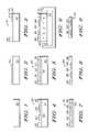
- FIG. 1is a cross sectional view of one embodiment of a carrier according to the present invention.
- FIG. 2is a cross sectional view of one embodiment of a carrier with adhesive tape applied on top thereof during a stage in the manufacture of a packaged integrated circuit according to the present invention.
- FIG. 3is a cross sectional view of one embodiment of a carrier, adhesive tape, and an encapsulant mold during another stage in the manufacture of a packaged integrated circuit according to the present invention.
- FIG. 4is a cross sectional view of one embodiment of a carrier, adhesive tape, an encapsulant mold, and IC die during another stage in the manufacture of a packaged integrated circuit according to the present invention.
- FIG. 5is a cross sectional view of one embodiment of a carrier, adhesive tape, an encapsulant mold, and an encapsulated structure during another stage in the manufacture of a packaged integrated circuit according to the present invention.
- FIG. 6is a cross sectional view of one embodiment of a carrier, adhesive tape, an encapsulant mold, and an encapsulated structure during another stage in the manufacture of a packaged integrated circuit according to the present invention.
- FIG. 7is a cross sectional view of one embodiment of adhesive tape, an encapsulant mold, and an encapsulated structure after the removal of the carrier during another stage in the manufacture of a packaged integrated circuit according to the present invention.
- FIG. 8is a cross sectional view of one embodiment of an encapsulant mold and an encapsulated structure after the removal of tape during another stage in the manufacture of a packaged integrated circuit according to the present invention.
- FIG. 9is a cross sectional view of one embodiment of an encapsulated structure after the removal of the encapsulant mold during another stage in the manufacture of a packaged integrated circuit according to the present invention.
- FIGS. 1–9show one embodiment of various stages of a process for encapsulating an IC die with the use of a porous carrier to allow for solvent to pass through the carrier to reduce the adhesive strength of an adhesive structure for the removal of a carrier from an encapsulated structure.
- FIG. 1is a cross sectional view of carrier 101 prior to the application of a tape for an encapsulating process.
- Carrier 101is porous in that has pores that allow a solvent to pass through from one side of the carrier to another side.
- carrier 101is made of a composite material of aluminum oxide embedded in a glass matrix.
- carrier 101may be made with other material such as e.g. metal, ceramics, glass, plastics, polymer or a combination thereof, where such materials are made to have a continuous open porosity.
- the carrieris made of a material that can withstand temperatures of the encapsulation process (e.g. 150 C).
- carrier 101has pores with a 0.2 micron diameter pore size and a coefficient of thermal expansion (CTE) of 8 parts per million (ppm).
- CTEcoefficient of thermal expansion
- the pore size of carrier 101may range from 0.02 microns up to 30 microns. In other embodiments, the pore size may be bigger. However, in some embodiments, a larger pore size may affect the smoothness of the surface of the carrier beyond a smoothness level that is desired. In one embodiment, the desired smoothness of the surface of the carrier is dependent upon the type of adhesive structure utilized for attachment of IC die. With some embodiments, the adhesive structure may be applied as a planar layer thereby allowing for a carrier to have larger pore sizes.
- a carrier with pores of a smaller pore sizemay be used. However, with a smaller pore size, a reduced amount of solvent passes thought the carrier. With some embodiments, the time needed for reducing the strength of the adhesive structure is dependent upon the amount of solvent passing through the carrier. Accordingly, with some embodiments, carriers with an open continuous porosity of a 0.02 micron diameter pour size or greater are utilized depending upon the amount of solvent desired to be passed through. Also, utilizing a carrier with pores of a smaller size may affect the reusability of the carrier in that the small pores may become clogged.
- carrier 101may have CTE of other values.
- the CTE of carrier 101is less than the CTE of an encapsulant used for encapsulating the IC die.
- the encapsulanthas a CTE ranging from 0.5–20 ppm.
- tape 203is applied to the top surface of carrier 101 .
- carrier 101Prior to applying tape 203 , carrier 101 is cleaned e.g. by baking and scrubbing.
- tape 203is a two sided adhesive tape.
- the die side (the top side in the view of FIG. 2 ) of tape 203has a silicone adhesive material with a thickness of 50 microns, but may be of other thicknesses (e.g. 12–100 microns) and/or of other adhesive materials (e.g. acrylic or organic) in other embodiments.
- the carrier side (the bottom side in the view of FIG. 2 ) of tape 203has a silicone adhesive material with a thickness of 75 microns.
- the carrier side adhesive materialmay be of other types of adhesive material (e.g. acrylic or organic) and/or may be of other thicknesses.
- the thickness of the carrier side adhesive materialshould be thick enough to fill in pores or other voids in the top side of carrier 101 so as to “planarize” the top surface of carrier 101 .
- the maximum thickness of the carrier side adhesive materialis limited by the ability to release the carrier from tape 203 with solvent.
- the thickness of the carrier side adhesive materialmay range from 12–100 microns, but may be of other thicknesses in other embodiments.
- the tapehas an adhesive material on the die side that is greater than 30 microns and an adhesive material on the carrier side that is greater than 50 microns.
- the silicone adhesivemay have additives to increase or decrease the silicone strength.
- the die side and carrier side adhesive materialsare separated by a tape carrier (e.g. polyester or polyamide).
- FIG. 3shows a cross sectional view of carrier 101 after an encapsulant mold is placed on top of tape 203 .
- Mold 305has an opening 307 for exposing the middle portion of tape 203 .
- integrated circuit die 403 and 405are placed on tape 203 in opening 307 in predefined locations.
- multiple dieare placed in an array configuration (e.g. 4 ⁇ 6, 6 ⁇ 6, or 8 ⁇ 8) on tape 203 .
- the dieare placed on tape 203 by a standard pick and place method, but may be placed on tape 203 by other methods.
- die 403 and 405include integrated circuits built on a semiconductor wafer which was subsequently singulated into separate die.
- die 403 and 405have a flip chip configuration and are placed active side down on tape 203 , wherein the bond pads (not show) are located on the bottom sides of die 403 and 405 relative to the view shown in FIG. 4 .
- an encapsulant materialis dispensed (e.g. with syringe and robotic needle) into opening 307 to form an encapsulant 503 that encapsulates die 403 and 405 in an encapsulated structure 505 .
- encapsulant 503may be formed by other encapsulating processes such as e.g. screen print, extrusion coating, transfer mold, ejection mold, glob top, or other encapsulating processes.
- the bottom portion of carrier 101is placed in a solvent bath 603 .
- Solvent from solvent bath 603is absorbed up through the carrier via a capillary action where it contacts the carrier side adhesive material of tape 203 .
- the solventbreaks down the adhesive strength of the carrier side adhesive material of tape 203 .
- the solventis acetone and the adhesive material is a silicone adhesive
- the solventsoftens the adhesive property of the silicone adhesive.
- the bottom portion of carrier 101is placed in bath 603 for about 5 minutes before carrier 101 separates from tape 203 .
- a greater portion of the carriermay be submerged in bath 603 .
- the entire carrier/mold/encapsulated structuremay be submerged in bath 603 .
- the carrier removal processmay be performed at room temperature, or in some embodiments, at least at temperatures below the transition temperature (T g ) of the encapsulant.
- T gtransition temperature
- the carriermay be removed from the encapsulated structure 505 without causing die 403 and 405 to drift within encapsulated structure 505 .
- the transition temperature of encapsulant 503is about 140 C.
- other types of encapsulant materialmay have a T g ranging from 90 C, to 200 C.
- FIG. 7shows a cross sectional view of mold 305 , encapsulated structure 505 , and tape 203 after carrier 101 has been removed.
- tape 203is pulled from encapsulated structure 505 and mold 305 .
- mold 305is removed from encapsulated structure 505 .
- structure 505is subject to further buildup processes (e.g. dielectric and metal interconnect processing) on the active side of the die to form interconnect structures (not shown). Encapsulated structure 505 is then singulated into a plurality of packaged ICs.
- each packaged ICincludes one IC die (e.g. 403 ). However, in other embodiments, each packaged IC may include multiple die (e.g. in stacked or side by side configurations). Also, package ICs of other embodiments may include stand alone devices (e.g. transistors, filters, capacitors, amplifiers) that are encapsulated in the encapsulant (e.g. 503 ). These additional items by be placed on tape 203 prior to encapsulation. In some embodiments, entire embedded systems (e.g. multichip modules, RF systems, or other wireless or information processing systems) may be included in a packaged IC.
- stand alone devicese.g. transistors, filters, capacitors, amplifiers
- a package substratemay be located between tape 203 and the IC die (e.g. 405 ) with, in some embodiments, the package substrate defining the bottom portion of the encapsulant.
- the IC dieare mounted to the packaged substrate, and then the package substrate is placed in opening 307 .
- the package substrateis first placed on tape 203 in opening 307 and then the IC die are placed on the substrate.
- the diemay be placed on the packaged substrate active side up wherein wire bonds are attached to bond pads on the active side and bond pads on the package substrate prior to encapsulation.
- tape 203may be used in place of tape 203 .
- two layers of tapemay be used for attaching an integrated circuit die.
- One layer of tapewould have adhesive material on two sides and the other layer would have adhesive on only one side.
- photo resist or other types of adhesivesmay be used as an adhesive structure for attaching the die to the carrier.
- a first layer of photo resist(not shown) would be applied to the top surface of carrier 101 .
- a second layer of photo resistis applied on the cured layer of photo resist.
- the IC dieare then placed on the second layer of photo resist. Afterwards, the second layer of photo resist is cured.
- a dry film photo resist or other adhesivemay be used where only one layer is used for attaching the die to the carrier.
- An example of one such adhesiveis RISTON as sold by DUPONT.
- acetone or N-Methyl 2-Pyrrolidonemay be used as a solvent that dissolves the photo resist or adhesive layer(s) (e.g. as when the bottom portion of carrier 101 is placed in a solvent bath).
- NMPN-Methyl 2-Pyrrolidone
- the adhesive structureis able to withstand curing temperatures for curing the encapsulant.
- a methodin one aspect of the invention, includes providing a porous carrier, providing an adhesive structure overlying the porous carrier, and placing a first integrated circuit die over the adhesive structure. The method also includes encapsulating the first integrated circuit die to form an encapsulated structure and separating the porous carrier from the encapsulated structure.
- a methodin another aspect of the invention, includes providing a porous carrier, adhering an adhesive structure to the porous carrier, and placing at least one integrated circuit die over the adhesive structure. The method also includes encapsulating the at least one integrated circuit die to form an encapsulated structure and removing the porous carrier from the encapsulated structure. The removing includes using a solvent that is passed through the porous carrier to reduce adhesive strength between the adhesive structure and the porous carrier.
- a methodin another aspect of the invention, includes providing a reusable porous carrier including pores with a pore size diameter of at least 0.02 microns, adhering an adhesive structure to the reusable porous carrier, and placing a plurality of integrated circuit die in an array configuration over the adhesive structure.
- the methodalso includes encapsulating the plurality of integrated circuit die to form an encapsulated structure and separating the reusable porous carrier from the encapsulated structure. The separating comprises using a solvent that is passed through the porous carrier to reduce adhesive strength between the adhesive structure and the reusable porous carrier.
Landscapes
- Engineering & Computer Science (AREA)
- Physics & Mathematics (AREA)
- Condensed Matter Physics & Semiconductors (AREA)
- General Physics & Mathematics (AREA)
- Manufacturing & Machinery (AREA)
- Computer Hardware Design (AREA)
- Microelectronics & Electronic Packaging (AREA)
- Power Engineering (AREA)
- Encapsulation Of And Coatings For Semiconductor Or Solid State Devices (AREA)
- Structures Or Materials For Encapsulating Or Coating Semiconductor Devices Or Solid State Devices (AREA)
- Wire Bonding (AREA)
Abstract
Description
Claims (34)
Priority Applications (6)
| Application Number | Priority Date | Filing Date | Title |
|---|---|---|---|
| US10/774,977US7015075B2 (en) | 2004-02-09 | 2004-02-09 | Die encapsulation using a porous carrier |
| CN2005800043966ACN1918702B (en) | 2004-02-09 | 2005-01-12 | Die encapsulation using a porous carrier |
| PCT/US2005/001529WO2005076794A2 (en) | 2004-02-09 | 2005-01-12 | Die encapsulation using a porous carrier |
| JP2006553132AJP4555835B2 (en) | 2004-02-09 | 2005-01-12 | Die encapsulation using porous carrier |
| EP05705847AEP1721332A2 (en) | 2004-02-09 | 2005-01-12 | Die encapsulation using a porous carrier |
| TW094102210ATWI389221B (en) | 2004-02-09 | 2005-01-25 | Die encapsulation method using a porous carrier |
Applications Claiming Priority (1)
| Application Number | Priority Date | Filing Date | Title |
|---|---|---|---|
| US10/774,977US7015075B2 (en) | 2004-02-09 | 2004-02-09 | Die encapsulation using a porous carrier |
Publications (2)
| Publication Number | Publication Date |
|---|---|
| US20050176180A1 US20050176180A1 (en) | 2005-08-11 |
| US7015075B2true US7015075B2 (en) | 2006-03-21 |
Family
ID=34827103
Family Applications (1)
| Application Number | Title | Priority Date | Filing Date |
|---|---|---|---|
| US10/774,977Expired - Fee RelatedUS7015075B2 (en) | 2004-02-09 | 2004-02-09 | Die encapsulation using a porous carrier |
Country Status (6)
| Country | Link |
|---|---|
| US (1) | US7015075B2 (en) |
| EP (1) | EP1721332A2 (en) |
| JP (1) | JP4555835B2 (en) |
| CN (1) | CN1918702B (en) |
| TW (1) | TWI389221B (en) |
| WO (1) | WO2005076794A2 (en) |
Cited By (83)
| Publication number | Priority date | Publication date | Assignee | Title |
|---|---|---|---|---|
| US7247523B1 (en) | 2002-11-08 | 2007-07-24 | Amkor Technology, Inc. | Two-sided wafer escape package |
| US7361533B1 (en) | 2002-11-08 | 2008-04-22 | Amkor Technology, Inc. | Stacked embedded leadframe |
| US20080113486A1 (en)* | 2006-09-29 | 2008-05-15 | Shingo Eguchi | Peeling apparatus and manufacturing apparatus of semiconductor device |
| US20080116560A1 (en)* | 2006-11-17 | 2008-05-22 | Mangrum Marc A | Method of packaging a device having a tangible element and device thereof |
| US20080119015A1 (en)* | 2006-11-17 | 2008-05-22 | Mangrum Marc A | Method of packaging a semiconductor device and a prefabricated connector |
| US20080132033A1 (en)* | 2006-09-29 | 2008-06-05 | Shingo Eguchi | Method for manufacturing semiconductor device |
| US7476563B2 (en) | 2006-11-17 | 2009-01-13 | Freescale Semiconductor, Inc. | Method of packaging a device using a dielectric layer |
| US20090102066A1 (en)* | 2007-10-22 | 2009-04-23 | Advanced Semiconductor Engineering, Inc. | Chip package structure and method of manufacturing the same |
| US7550857B1 (en) | 2006-11-16 | 2009-06-23 | Amkor Technology, Inc. | Stacked redistribution layer (RDL) die assembly package |
| US20090165293A1 (en)* | 2007-12-27 | 2009-07-02 | Freescale Semiconductor, Inc. | Electronic assembly manufacturing method |
| US7572681B1 (en) | 2005-12-08 | 2009-08-11 | Amkor Technology, Inc. | Embedded electronic component package |
| US20090221114A1 (en)* | 2008-02-29 | 2009-09-03 | Freescale Semiconductor, Inc. | Packaging an integrated circuit die using compression molding |
| US7633765B1 (en) | 2004-03-23 | 2009-12-15 | Amkor Technology, Inc. | Semiconductor package including a top-surface metal layer for implementing circuit features |
| US7671457B1 (en) | 2002-05-01 | 2010-03-02 | Amkor Technology, Inc. | Semiconductor package including top-surface terminals for mounting another semiconductor package |
| US20100112756A1 (en)* | 2008-11-06 | 2010-05-06 | Amrine Craig S | Integrated circuit package formation |
| US7723210B2 (en) | 2002-11-08 | 2010-05-25 | Amkor Technology, Inc. | Direct-write wafer level chip scale package |
| US7807511B2 (en) | 2006-11-17 | 2010-10-05 | Freescale Semiconductor, Inc. | Method of packaging a device having a multi-contact elastomer connector contact area and device thereof |
| US20100320593A1 (en)* | 2009-06-19 | 2010-12-23 | Advanced Semiconductor Engineering, Inc. | Chip Package Structure and Manufacturing Methods Thereof |
| US20110018124A1 (en)* | 2009-07-23 | 2011-01-27 | Advanced Semiconductor Engineering, Inc. | Semiconductor Device Packages, Redistribution Structures, and Manufacturing Methods Thereof |
| US20110018118A1 (en)* | 2009-07-21 | 2011-01-27 | Advanced Semiconductor Engineering, Inc. | Semiconductor Device Packages, Redistribution Structures, and Manufacturing Methods Thereof |
| US7902660B1 (en) | 2006-05-24 | 2011-03-08 | Amkor Technology, Inc. | Substrate for semiconductor device and manufacturing method thereof |
| US20110084372A1 (en)* | 2009-10-14 | 2011-04-14 | Advanced Semiconductor Engineering, Inc. | Package carrier, semiconductor package, and process for fabricating same |
| US20110115060A1 (en)* | 2009-11-19 | 2011-05-19 | Advanced Semiconductor Engineering, Inc. | Wafer-Level Semiconductor Device Packages with Electromagnetic Interference Shielding |
| US20110119910A1 (en)* | 2009-11-23 | 2011-05-26 | Freescale Semiconductor, Inc. | Method and system for releasing a microelectronic assembly from a carrier substrate |
| US20110127654A1 (en)* | 2009-11-27 | 2011-06-02 | Advanced Semiconductor Engineering, Inc.., | Semiconductor Package and Manufacturing Methods Thereof |
| US7960827B1 (en) | 2009-04-09 | 2011-06-14 | Amkor Technology, Inc. | Thermal via heat spreader package and method |
| US20110169150A1 (en)* | 2010-01-13 | 2011-07-14 | Advanced Semiconductor Engineering, Inc. | Semiconductor Package with Single Sided Substrate Design and Manufacturing Methods Thereof |
| US20110177654A1 (en)* | 2010-01-21 | 2011-07-21 | Advanced Semiconductor Engineering, Inc. | Wafer-Level Semiconductor Device Packages with Three-Dimensional Fan-Out and Manufacturing Methods Thereof |
| US20110194265A1 (en)* | 2010-02-05 | 2011-08-11 | Advanced Semiconductor Engineering, Inc. | Embedded Component Substrate and Manufacturing Methods Thereof |
| US20110227220A1 (en)* | 2010-03-22 | 2011-09-22 | Chia-Ching Chen | Stackable semiconductor package and manufacturing method thereof |
| US8222538B1 (en) | 2009-06-12 | 2012-07-17 | Amkor Technology, Inc. | Stackable via package and method |
| US8278746B2 (en) | 2010-04-02 | 2012-10-02 | Advanced Semiconductor Engineering, Inc. | Semiconductor device packages including connecting elements |
| US8294276B1 (en) | 2010-05-27 | 2012-10-23 | Amkor Technology, Inc. | Semiconductor device and fabricating method thereof |
| US8300423B1 (en) | 2010-05-25 | 2012-10-30 | Amkor Technology, Inc. | Stackable treated via package and method |
| US8324511B1 (en) | 2010-04-06 | 2012-12-04 | Amkor Technology, Inc. | Through via nub reveal method and structure |
| US8338229B1 (en) | 2010-07-30 | 2012-12-25 | Amkor Technology, Inc. | Stackable plasma cleaned via package and method |
| US8337657B1 (en) | 2010-10-27 | 2012-12-25 | Amkor Technology, Inc. | Mechanical tape separation package and method |
| US8341835B1 (en) | 2002-05-01 | 2013-01-01 | Amkor Technology, Inc. | Buildup dielectric layer having metallization pattern semiconductor package fabrication method |
| US8390130B1 (en) | 2011-01-06 | 2013-03-05 | Amkor Technology, Inc. | Through via recessed reveal structure and method |
| US8440554B1 (en) | 2010-08-02 | 2013-05-14 | Amkor Technology, Inc. | Through via connected backside embedded circuit features structure and method |
| US8471154B1 (en) | 2009-08-06 | 2013-06-25 | Amkor Technology, Inc. | Stackable variable height via package and method |
| US8482134B1 (en) | 2010-11-01 | 2013-07-09 | Amkor Technology, Inc. | Stackable package and method |
| US8487445B1 (en) | 2010-10-05 | 2013-07-16 | Amkor Technology, Inc. | Semiconductor device having through electrodes protruding from dielectric layer |
| US20130217186A1 (en)* | 2012-02-16 | 2013-08-22 | Fujitsu Limited | Method of manufacturing semiconductor device and method of manufacturing electronic assembly |
| US8525318B1 (en) | 2010-11-10 | 2013-09-03 | Amkor Technology, Inc. | Semiconductor device and fabricating method thereof |
| US8536462B1 (en) | 2010-01-22 | 2013-09-17 | Amkor Technology, Inc. | Flex circuit package and method |
| US8535961B1 (en) | 2010-12-09 | 2013-09-17 | Amkor Technology, Inc. | Light emitting diode (LED) package and method |
| US8552548B1 (en) | 2011-11-29 | 2013-10-08 | Amkor Technology, Inc. | Conductive pad on protruding through electrode semiconductor device |
| US8557629B1 (en) | 2010-12-03 | 2013-10-15 | Amkor Technology, Inc. | Semiconductor device having overlapped via apertures |
| US8624374B2 (en) | 2010-04-02 | 2014-01-07 | Advanced Semiconductor Engineering, Inc. | Semiconductor device packages with fan-out and with connecting elements for stacking and manufacturing methods thereof |
| US8623753B1 (en) | 2009-05-28 | 2014-01-07 | Amkor Technology, Inc. | Stackable protruding via package and method |
| US8633598B1 (en) | 2011-09-20 | 2014-01-21 | Amkor Technology, Inc. | Underfill contacting stacking balls package fabrication method and structure |
| US8653674B1 (en) | 2011-09-15 | 2014-02-18 | Amkor Technology, Inc. | Electronic component package fabrication method and structure |
| US8717775B1 (en) | 2010-08-02 | 2014-05-06 | Amkor Technology, Inc. | Fingerprint sensor package and method |
| US8791501B1 (en) | 2010-12-03 | 2014-07-29 | Amkor Technology, Inc. | Integrated passive device structure and method |
| US8796561B1 (en) | 2009-10-05 | 2014-08-05 | Amkor Technology, Inc. | Fan out build up substrate stackable package and method |
| US8890329B2 (en) | 2011-04-26 | 2014-11-18 | Amkor Technology, Inc. | Semiconductor device |
| US8937381B1 (en) | 2009-12-03 | 2015-01-20 | Amkor Technology, Inc. | Thin stackable package and method |
| US8941222B2 (en) | 2010-11-11 | 2015-01-27 | Advanced Semiconductor Engineering Inc. | Wafer level semiconductor package and manufacturing methods thereof |
| US8946883B2 (en) | 2012-09-20 | 2015-02-03 | Amkor Technology, Inc. | Wafer level fan-out package with a fiducial die |
| US9013011B1 (en) | 2011-03-11 | 2015-04-21 | Amkor Technology, Inc. | Stacked and staggered die MEMS package and method |
| US9029962B1 (en) | 2011-10-12 | 2015-05-12 | Amkor Technology, Inc. | Molded cavity substrate MEMS package fabrication method and structure |
| US9048342B2 (en) | 2011-12-21 | 2015-06-02 | Industrial Technology Research Institute | Semiconductor device stacked structure |
| US9048298B1 (en) | 2012-03-29 | 2015-06-02 | Amkor Technology, Inc. | Backside warpage control structure and fabrication method |
| US9129943B1 (en) | 2012-03-29 | 2015-09-08 | Amkor Technology, Inc. | Embedded component package and fabrication method |
| US9391043B2 (en) | 2012-11-20 | 2016-07-12 | Amkor Technology, Inc. | Semiconductor device and manufacturing method thereof |
| US9406639B2 (en) | 2012-08-08 | 2016-08-02 | Amkor Technology, Inc. | Semiconductor package and manufacturing method thereof |
| US9406658B2 (en) | 2010-12-17 | 2016-08-02 | Advanced Semiconductor Engineering, Inc. | Embedded component device and manufacturing methods thereof |
| US9543242B1 (en) | 2013-01-29 | 2017-01-10 | Amkor Technology, Inc. | Semiconductor package and fabricating method thereof |
| US9691635B1 (en) | 2002-05-01 | 2017-06-27 | Amkor Technology, Inc. | Buildup dielectric layer having metallization pattern semiconductor package fabrication method |
| US9691734B1 (en) | 2009-12-07 | 2017-06-27 | Amkor Technology, Inc. | Method of forming a plurality of electronic component packages |
| US9704842B2 (en) | 2013-11-04 | 2017-07-11 | Amkor Technology, Inc. | Interposer, manufacturing method thereof, semiconductor package using the same, and method for fabricating the semiconductor package |
| US9704747B2 (en) | 2013-03-29 | 2017-07-11 | Amkor Technology, Inc. | Semiconductor device and manufacturing method thereof |
| US9721872B1 (en) | 2011-02-18 | 2017-08-01 | Amkor Technology, Inc. | Methods and structures for increasing the allowable die size in TMV packages |
| US9735398B2 (en) | 2013-08-06 | 2017-08-15 | Semiconductor Energy Laboratory Co., Ltd. | Peeling method |
| US9748154B1 (en) | 2010-11-04 | 2017-08-29 | Amkor Technology, Inc. | Wafer level fan out semiconductor device and manufacturing method thereof |
| US9773998B2 (en) | 2013-09-06 | 2017-09-26 | Semiconductor Energy Laboratory Co., Ltd. | Light-emitting device and method for manufacturing light-emitting device |
| US9799829B2 (en) | 2014-07-25 | 2017-10-24 | Semiconductor Energy Laboratory Co., Ltd. | Separation method, light-emitting device, module, and electronic device |
| US9937698B2 (en) | 2013-11-06 | 2018-04-10 | Semiconductor Energy Laboratory Co., Ltd. | Peeling method and light-emitting device |
| US9960328B2 (en) | 2016-09-06 | 2018-05-01 | Amkor Technology, Inc. | Semiconductor device and manufacturing method thereof |
| US10259207B2 (en) | 2016-01-26 | 2019-04-16 | Semiconductor Energy Laboratory Co., Ltd. | Method for forming separation starting point and separation method |
| US10811277B2 (en) | 2004-03-23 | 2020-10-20 | Amkor Technology, Inc. | Encapsulated semiconductor package |
| US11081370B2 (en) | 2004-03-23 | 2021-08-03 | Amkor Technology Singapore Holding Pte. Ltd. | Methods of manufacturing an encapsulated semiconductor device |
Families Citing this family (5)
| Publication number | Priority date | Publication date | Assignee | Title |
|---|---|---|---|---|
| US20070212813A1 (en)* | 2006-03-10 | 2007-09-13 | Fay Owen R | Perforated embedded plane package and method |
| US20080182363A1 (en)* | 2007-01-31 | 2008-07-31 | Freescale Semiconductor, Inc. | Method for forming a microelectronic assembly including encapsulating a die using a sacrificial layer |
| ATE551722T1 (en) | 2008-06-26 | 2012-04-15 | Nxp Bv | ENCAPSULATED SEMICONDUCTOR PRODUCT AND METHOD FOR PRODUCING IT |
| JP5586920B2 (en)* | 2008-11-20 | 2014-09-10 | 株式会社半導体エネルギー研究所 | Method for manufacturing flexible semiconductor device |
| US10147630B2 (en)* | 2014-06-11 | 2018-12-04 | John Cleaon Moore | Sectional porous carrier forming a temporary impervious support |
Citations (15)
| Publication number | Priority date | Publication date | Assignee | Title |
|---|---|---|---|---|
| US4918811A (en) | 1986-09-26 | 1990-04-24 | General Electric Company | Multichip integrated circuit packaging method |
| US5032543A (en) | 1988-06-17 | 1991-07-16 | Massachusetts Institute Of Technology | Coplanar packaging techniques for multichip circuits |
| US5144747A (en) | 1991-03-27 | 1992-09-08 | Integrated System Assemblies Corporation | Apparatus and method for positioning an integrated circuit chip within a multichip module |
| US5250843A (en) | 1991-03-27 | 1993-10-05 | Integrated System Assemblies Corp. | Multichip integrated circuit modules |
| US5620928A (en)* | 1995-05-11 | 1997-04-15 | National Semiconductor Corporation | Ultra thin ball grid array using a flex tape or printed wiring board substrate and method |
| US5830800A (en)* | 1997-04-11 | 1998-11-03 | Compeq Manufacturing Company Ltd. | Packaging method for a ball grid array integrated circuit without utilizing a base plate |
| US5866952A (en) | 1995-11-30 | 1999-02-02 | Lockheed Martin Corporation | High density interconnected circuit module with a compliant layer as part of a stress-reducing molded substrate |
| US6036173A (en)* | 1997-11-25 | 2000-03-14 | Siemens Aktiengesellschaft | Semiconductor element having a carrying device and a lead frame and a semiconductor chip connected thereto |
| US6159767A (en) | 1996-05-20 | 2000-12-12 | Epic Technologies, Inc. | Single chip modules, repairable multichip modules, and methods of fabrication thereof |
| US6319828B1 (en)* | 1998-06-24 | 2001-11-20 | Samsung Electronics Co., Ltd. | Method for manufacturing a chip scale package having copper traces selectively plated with gold |
| US6370293B1 (en)* | 1999-09-16 | 2002-04-09 | Lucent Technologies, Inc. | Flexible optical circuits having optical fibers encapsulated between porous substrates and methods for fabricating same |
| WO2002033751A2 (en) | 2000-10-19 | 2002-04-25 | Intel Corporation | Microelectronic substrate with integrated devices |
| JP2002362677A (en)* | 2001-06-06 | 2002-12-18 | Nitto Denko Corp | Carrier tape for chip-like electronic components and method of using the same |
| US6528145B1 (en)* | 2000-06-29 | 2003-03-04 | International Business Machines Corporation | Polymer and ceramic composite electronic substrates |
| US6613413B1 (en)* | 1999-04-26 | 2003-09-02 | International Business Machines Corporation | Porous power and ground planes for reduced PCB delamination and better reliability |
Family Cites Families (5)
| Publication number | Priority date | Publication date | Assignee | Title |
|---|---|---|---|---|
| US5474958A (en)* | 1993-05-04 | 1995-12-12 | Motorola, Inc. | Method for making semiconductor device having no die supporting surface |
| JP2001313350A (en)* | 2000-04-28 | 2001-11-09 | Sony Corp | Chip-shaped electronic component and its manufacturing method, and pseudo-wafer used for manufacture of chip- shaped electronic component and its manufacturing method |
| KR100414479B1 (en)* | 2000-08-09 | 2004-01-07 | 주식회사 코스타트반도체 | Implantable circuit tapes for implanted semiconductor package and method for manufacturing thereof |
| JP4100936B2 (en)* | 2002-03-01 | 2008-06-11 | Necエレクトロニクス株式会社 | Manufacturing method of semiconductor device |
| JP2003303919A (en)* | 2002-04-10 | 2003-10-24 | Hitachi Ltd | Semiconductor device and manufacturing method thereof |
- 2004
- 2004-02-09USUS10/774,977patent/US7015075B2/ennot_activeExpired - Fee Related
- 2005
- 2005-01-12CNCN2005800043966Apatent/CN1918702B/ennot_activeExpired - Fee Related
- 2005-01-12JPJP2006553132Apatent/JP4555835B2/ennot_activeExpired - Fee Related
- 2005-01-12WOPCT/US2005/001529patent/WO2005076794A2/enactiveApplication Filing
- 2005-01-12EPEP05705847Apatent/EP1721332A2/ennot_activeWithdrawn
- 2005-01-25TWTW094102210Apatent/TWI389221B/ennot_activeIP Right Cessation
Patent Citations (15)
| Publication number | Priority date | Publication date | Assignee | Title |
|---|---|---|---|---|
| US4918811A (en) | 1986-09-26 | 1990-04-24 | General Electric Company | Multichip integrated circuit packaging method |
| US5032543A (en) | 1988-06-17 | 1991-07-16 | Massachusetts Institute Of Technology | Coplanar packaging techniques for multichip circuits |
| US5144747A (en) | 1991-03-27 | 1992-09-08 | Integrated System Assemblies Corporation | Apparatus and method for positioning an integrated circuit chip within a multichip module |
| US5250843A (en) | 1991-03-27 | 1993-10-05 | Integrated System Assemblies Corp. | Multichip integrated circuit modules |
| US5620928A (en)* | 1995-05-11 | 1997-04-15 | National Semiconductor Corporation | Ultra thin ball grid array using a flex tape or printed wiring board substrate and method |
| US5866952A (en) | 1995-11-30 | 1999-02-02 | Lockheed Martin Corporation | High density interconnected circuit module with a compliant layer as part of a stress-reducing molded substrate |
| US6159767A (en) | 1996-05-20 | 2000-12-12 | Epic Technologies, Inc. | Single chip modules, repairable multichip modules, and methods of fabrication thereof |
| US5830800A (en)* | 1997-04-11 | 1998-11-03 | Compeq Manufacturing Company Ltd. | Packaging method for a ball grid array integrated circuit without utilizing a base plate |
| US6036173A (en)* | 1997-11-25 | 2000-03-14 | Siemens Aktiengesellschaft | Semiconductor element having a carrying device and a lead frame and a semiconductor chip connected thereto |
| US6319828B1 (en)* | 1998-06-24 | 2001-11-20 | Samsung Electronics Co., Ltd. | Method for manufacturing a chip scale package having copper traces selectively plated with gold |
| US6613413B1 (en)* | 1999-04-26 | 2003-09-02 | International Business Machines Corporation | Porous power and ground planes for reduced PCB delamination and better reliability |
| US6370293B1 (en)* | 1999-09-16 | 2002-04-09 | Lucent Technologies, Inc. | Flexible optical circuits having optical fibers encapsulated between porous substrates and methods for fabricating same |
| US6528145B1 (en)* | 2000-06-29 | 2003-03-04 | International Business Machines Corporation | Polymer and ceramic composite electronic substrates |
| WO2002033751A2 (en) | 2000-10-19 | 2002-04-25 | Intel Corporation | Microelectronic substrate with integrated devices |
| JP2002362677A (en)* | 2001-06-06 | 2002-12-18 | Nitto Denko Corp | Carrier tape for chip-like electronic components and method of using the same |
Non-Patent Citations (1)
| Title |
|---|
| JP 2002-362677 A, Dec. 2002, Takaoka et al., Translation.* |
Cited By (199)
| Publication number | Priority date | Publication date | Assignee | Title |
|---|---|---|---|---|
| US7671457B1 (en) | 2002-05-01 | 2010-03-02 | Amkor Technology, Inc. | Semiconductor package including top-surface terminals for mounting another semiconductor package |
| US8341835B1 (en) | 2002-05-01 | 2013-01-01 | Amkor Technology, Inc. | Buildup dielectric layer having metallization pattern semiconductor package fabrication method |
| US8110909B1 (en) | 2002-05-01 | 2012-02-07 | Amkor Technology, Inc. | Semiconductor package including top-surface terminals for mounting another semiconductor package |
| US8026587B1 (en) | 2002-05-01 | 2011-09-27 | Amkor Technology, Inc. | Semiconductor package including top-surface terminals for mounting another semiconductor package |
| US9691635B1 (en) | 2002-05-01 | 2017-06-27 | Amkor Technology, Inc. | Buildup dielectric layer having metallization pattern semiconductor package fabrication method |
| US9812386B1 (en) | 2002-05-01 | 2017-11-07 | Amkor Technology, Inc. | Encapsulated semiconductor package |
| US10461006B1 (en) | 2002-05-01 | 2019-10-29 | Amkor Technology, Inc. | Encapsulated semiconductor package |
| US9406645B1 (en) | 2002-11-08 | 2016-08-02 | Amkor Technology, Inc. | Wafer level package and fabrication method |
| US7420272B1 (en) | 2002-11-08 | 2008-09-02 | Amkor Technology, Inc. | Two-sided wafer escape package |
| US8501543B1 (en) | 2002-11-08 | 2013-08-06 | Amkor Technology, Inc. | Direct-write wafer level chip scale package |
| US7361533B1 (en) | 2002-11-08 | 2008-04-22 | Amkor Technology, Inc. | Stacked embedded leadframe |
| US8691632B1 (en) | 2002-11-08 | 2014-04-08 | Amkor Technology, Inc. | Wafer level package and fabrication method |
| US7247523B1 (en) | 2002-11-08 | 2007-07-24 | Amkor Technology, Inc. | Two-sided wafer escape package |
| US8710649B1 (en) | 2002-11-08 | 2014-04-29 | Amkor Technology, Inc. | Wafer level package and fabrication method |
| US8952522B1 (en) | 2002-11-08 | 2015-02-10 | Amkor Technology, Inc. | Wafer level package and fabrication method |
| US10665567B1 (en) | 2002-11-08 | 2020-05-26 | Amkor Technology, Inc. | Wafer level package and fabrication method |
| US9054117B1 (en) | 2002-11-08 | 2015-06-09 | Amkor Technology, Inc. | Wafer level package and fabrication method |
| US8298866B1 (en) | 2002-11-08 | 2012-10-30 | Amkor Technology, Inc. | Wafer level package and fabrication method |
| US7932595B1 (en) | 2002-11-08 | 2011-04-26 | Amkor Technology, Inc. | Electronic component package comprising fan-out traces |
| US9871015B1 (en) | 2002-11-08 | 2018-01-16 | Amkor Technology, Inc. | Wafer level package and fabrication method |
| US8486764B1 (en) | 2002-11-08 | 2013-07-16 | Amkor Technology, Inc. | Wafer level package and fabrication method |
| US8188584B1 (en) | 2002-11-08 | 2012-05-29 | Amkor Technology, Inc. | Direct-write wafer level chip scale package |
| US7692286B1 (en) | 2002-11-08 | 2010-04-06 | Amkor Technology, Inc. | Two-sided fan-out wafer escape package |
| US8119455B1 (en) | 2002-11-08 | 2012-02-21 | Amkor Technology, Inc. | Wafer level package fabrication method |
| US7723210B2 (en) | 2002-11-08 | 2010-05-25 | Amkor Technology, Inc. | Direct-write wafer level chip scale package |
| US7714431B1 (en) | 2002-11-08 | 2010-05-11 | Amkor Technology, Inc. | Electronic component package comprising fan-out and fan-in traces |
| US8018068B1 (en) | 2004-03-23 | 2011-09-13 | Amkor Technology, Inc. | Semiconductor package including a top-surface metal layer for implementing circuit features |
| US7633765B1 (en) | 2004-03-23 | 2009-12-15 | Amkor Technology, Inc. | Semiconductor package including a top-surface metal layer for implementing circuit features |
| US8227338B1 (en) | 2004-03-23 | 2012-07-24 | Amkor Technology, Inc. | Semiconductor package including a top-surface metal layer for implementing circuit features |
| US11094560B1 (en) | 2004-03-23 | 2021-08-17 | Amkor Technology Singapore Holding Pte. Ltd. | Encapsulated semiconductor package |
| US11081370B2 (en) | 2004-03-23 | 2021-08-03 | Amkor Technology Singapore Holding Pte. Ltd. | Methods of manufacturing an encapsulated semiconductor device |
| US10811277B2 (en) | 2004-03-23 | 2020-10-20 | Amkor Technology, Inc. | Encapsulated semiconductor package |
| US7977163B1 (en) | 2005-12-08 | 2011-07-12 | Amkor Technology, Inc. | Embedded electronic component package fabrication method |
| US7572681B1 (en) | 2005-12-08 | 2009-08-11 | Amkor Technology, Inc. | Embedded electronic component package |
| US7902660B1 (en) | 2006-05-24 | 2011-03-08 | Amkor Technology, Inc. | Substrate for semiconductor device and manufacturing method thereof |
| US11848214B2 (en) | 2006-08-01 | 2023-12-19 | Amkor Technology Singapore Holding Pte. Ltd. | Encapsulated semiconductor package |
| US20090017599A1 (en)* | 2006-09-29 | 2009-01-15 | Semiconductor Energy Laboratory Co., Ltd. | Method for manufacturing semiconductor device |
| US8137417B2 (en) | 2006-09-29 | 2012-03-20 | Semiconductor Energy Laboratory Co., Ltd. | Peeling apparatus and manufacturing apparatus of semiconductor device |
| US20090017567A1 (en)* | 2006-09-29 | 2009-01-15 | Semiconductor Energy Laboratory Co., Ltd. | Method for manufacturing semiconductor device |
| US10134784B2 (en) | 2006-09-29 | 2018-11-20 | Semiconductor Energy Laboratory Co., Ltd. | Peeling apparatus and manufacturing apparatus of semiconductor device |
| US20080132033A1 (en)* | 2006-09-29 | 2008-06-05 | Shingo Eguchi | Method for manufacturing semiconductor device |
| US20090023251A1 (en)* | 2006-09-29 | 2009-01-22 | Semiconductor Energy Laboratory Co., Ltd. | Method for manufacturing semiconductor device |
| US8889438B2 (en) | 2006-09-29 | 2014-11-18 | Semiconductor Energy Laboratory Co., Ltd. | Peeling apparatus and manufacturing apparatus of semiconductor device |
| US9054141B2 (en) | 2006-09-29 | 2015-06-09 | Semiconductor Energy Laboratory Co., Ltd. | Method for manufacturing semiconductor device |
| US9087931B2 (en) | 2006-09-29 | 2015-07-21 | Semiconductor Energy Laboratory Co., Ltd. | Peeling apparatus and manufacturing apparatus of semiconductor device |
| US9397126B2 (en) | 2006-09-29 | 2016-07-19 | Semiconductor Energy Laboratory Co., Ltd. | Peeling apparatus and manufacturing apparatus of semiconductor device |
| US9570329B2 (en) | 2006-09-29 | 2017-02-14 | Semiconductor Energy Laboratory Co., Ltd. | Peeling apparatus and manufacturing apparatus of semiconductor device |
| US9472429B2 (en) | 2006-09-29 | 2016-10-18 | Semiconductor Energy Laboratory Co., Ltd. | Method for manufacturing semiconductor device |
| US20080113486A1 (en)* | 2006-09-29 | 2008-05-15 | Shingo Eguchi | Peeling apparatus and manufacturing apparatus of semiconductor device |
| US8043936B2 (en) | 2006-09-29 | 2011-10-25 | Semiconductor Energy Laboratory Co., Ltd. | Method for manufacturing semiconductor device |
| US8048777B2 (en) | 2006-09-29 | 2011-11-01 | Semiconductor Energy Laboratory Co., Ltd. | Method for manufacturing semiconductor device |
| US8048770B2 (en) | 2006-09-29 | 2011-11-01 | Semiconductor Energy Laboratory Co., Ltd. | Method for manufacturing semiconductor device |
| US8203203B1 (en) | 2006-11-16 | 2012-06-19 | Amkor Technology, Inc. | Stacked redistribution layer (RDL) die assembly package |
| US8629546B1 (en) | 2006-11-16 | 2014-01-14 | Amkor Technology, Inc. | Stacked redistribution layer (RDL) die assembly package |
| US7550857B1 (en) | 2006-11-16 | 2009-06-23 | Amkor Technology, Inc. | Stacked redistribution layer (RDL) die assembly package |
| US7825520B1 (en) | 2006-11-16 | 2010-11-02 | Amkor Technology, Inc. | Stacked redistribution layer (RDL) die assembly package |
| US7588951B2 (en) | 2006-11-17 | 2009-09-15 | Freescale Semiconductor, Inc. | Method of packaging a semiconductor device and a prefabricated connector |
| US7696016B2 (en) | 2006-11-17 | 2010-04-13 | Freescale Semiconductor, Inc. | Method of packaging a device having a tangible element and device thereof |
| US7476563B2 (en) | 2006-11-17 | 2009-01-13 | Freescale Semiconductor, Inc. | Method of packaging a device using a dielectric layer |
| US7807511B2 (en) | 2006-11-17 | 2010-10-05 | Freescale Semiconductor, Inc. | Method of packaging a device having a multi-contact elastomer connector contact area and device thereof |
| US20090286390A1 (en)* | 2006-11-17 | 2009-11-19 | Freescale Semiconductor, Inc. | Method of packaging a semiconductor device and a prefabricated connector |
| US7655502B2 (en) | 2006-11-17 | 2010-02-02 | Freescale Semiconductor, Inc. | Method of packaging a semiconductor device and a prefabricated connector |
| US20080119015A1 (en)* | 2006-11-17 | 2008-05-22 | Mangrum Marc A | Method of packaging a semiconductor device and a prefabricated connector |
| US20080116560A1 (en)* | 2006-11-17 | 2008-05-22 | Mangrum Marc A | Method of packaging a device having a tangible element and device thereof |
| US8035213B2 (en) | 2007-10-22 | 2011-10-11 | Advanced Semiconductor Engineering, Inc. | Chip package structure and method of manufacturing the same |
| US20090102066A1 (en)* | 2007-10-22 | 2009-04-23 | Advanced Semiconductor Engineering, Inc. | Chip package structure and method of manufacturing the same |
| CN101904003B (en)* | 2007-12-27 | 2012-08-08 | 飞思卡尔半导体公司 | Electronic assembly manufacturing method |
| US20090165293A1 (en)* | 2007-12-27 | 2009-07-02 | Freescale Semiconductor, Inc. | Electronic assembly manufacturing method |
| WO2009085463A1 (en)* | 2007-12-27 | 2009-07-09 | Freescale Semiconductor Inc. | Electronic assembly manufacturing method |
| US7802359B2 (en) | 2007-12-27 | 2010-09-28 | Freescale Semiconductor, Inc. | Electronic assembly manufacturing method |
| US20090221114A1 (en)* | 2008-02-29 | 2009-09-03 | Freescale Semiconductor, Inc. | Packaging an integrated circuit die using compression molding |
| US8609471B2 (en) | 2008-02-29 | 2013-12-17 | Freescale Semiconductor, Inc. | Packaging an integrated circuit die using compression molding |
| US7741151B2 (en) | 2008-11-06 | 2010-06-22 | Freescale Semiconductor, Inc. | Integrated circuit package formation |
| US20100112756A1 (en)* | 2008-11-06 | 2010-05-06 | Amrine Craig S | Integrated circuit package formation |
| US7960827B1 (en) | 2009-04-09 | 2011-06-14 | Amkor Technology, Inc. | Thermal via heat spreader package and method |
| US8623753B1 (en) | 2009-05-28 | 2014-01-07 | Amkor Technology, Inc. | Stackable protruding via package and method |
| US8704368B1 (en) | 2009-06-12 | 2014-04-22 | Amkor Technology, Inc. | Stackable via package and method |
| US10034372B1 (en) | 2009-06-12 | 2018-07-24 | Amkor Technology, Inc. | Stackable via package and method |
| US10206285B1 (en) | 2009-06-12 | 2019-02-12 | Amkor Technology, Inc. | Stackable via package and method |
| US12035472B2 (en) | 2009-06-12 | 2024-07-09 | Amkor Technology Singapore Holding Ptd. Ltd. | Stackable via package and method |
| US10548221B1 (en) | 2009-06-12 | 2020-01-28 | Amkor Technology, Inc. | Stackable via package and method |
| US8222538B1 (en) | 2009-06-12 | 2012-07-17 | Amkor Technology, Inc. | Stackable via package and method |
| US11700692B2 (en) | 2009-06-12 | 2023-07-11 | Amkor Technology Singapore Holding Pte. Ltd. | Stackable via package and method |
| US9730327B1 (en) | 2009-06-12 | 2017-08-08 | Amkor Technology, Inc. | Stackable via package and method |
| US11089685B2 (en) | 2009-06-12 | 2021-08-10 | Amkor Technology Singapore Holding Pte. Ltd. | Stackable via package and method |
| US9012789B1 (en) | 2009-06-12 | 2015-04-21 | Amkor Technology, Inc. | Stackable via package and method |
| US8110916B2 (en) | 2009-06-19 | 2012-02-07 | Advanced Semiconductor Engineering, Inc. | Chip package structure and manufacturing methods thereof |
| US20100320593A1 (en)* | 2009-06-19 | 2010-12-23 | Advanced Semiconductor Engineering, Inc. | Chip Package Structure and Manufacturing Methods Thereof |
| US20110018118A1 (en)* | 2009-07-21 | 2011-01-27 | Advanced Semiconductor Engineering, Inc. | Semiconductor Device Packages, Redistribution Structures, and Manufacturing Methods Thereof |
| US8193647B2 (en) | 2009-07-21 | 2012-06-05 | Advanced Semiconductor Engineering, Inc. | Semiconductor device package with an alignment mark |
| US20110018124A1 (en)* | 2009-07-23 | 2011-01-27 | Advanced Semiconductor Engineering, Inc. | Semiconductor Device Packages, Redistribution Structures, and Manufacturing Methods Thereof |
| US8358001B2 (en) | 2009-07-23 | 2013-01-22 | Advanced Semiconductor Engineering, Inc. | Semiconductor device packages, redistribution structures, and manufacturing methods thereof |
| US10257942B1 (en) | 2009-08-06 | 2019-04-09 | Amkor Technology, Inc. | Stackable variable height via package and method |
| US8471154B1 (en) | 2009-08-06 | 2013-06-25 | Amkor Technology, Inc. | Stackable variable height via package and method |
| US8796561B1 (en) | 2009-10-05 | 2014-08-05 | Amkor Technology, Inc. | Fan out build up substrate stackable package and method |
| US20110084372A1 (en)* | 2009-10-14 | 2011-04-14 | Advanced Semiconductor Engineering, Inc. | Package carrier, semiconductor package, and process for fabricating same |
| US9564346B2 (en) | 2009-10-14 | 2017-02-07 | Advanced Semiconductor Engineering, Inc. | Package carrier, semiconductor package, and process for fabricating same |
| US8378466B2 (en) | 2009-11-19 | 2013-02-19 | Advanced Semiconductor Engineering, Inc. | Wafer-level semiconductor device packages with electromagnetic interference shielding |
| US20110115060A1 (en)* | 2009-11-19 | 2011-05-19 | Advanced Semiconductor Engineering, Inc. | Wafer-Level Semiconductor Device Packages with Electromagnetic Interference Shielding |
| US20110119910A1 (en)* | 2009-11-23 | 2011-05-26 | Freescale Semiconductor, Inc. | Method and system for releasing a microelectronic assembly from a carrier substrate |
| US8327532B2 (en)* | 2009-11-23 | 2012-12-11 | Freescale Semiconductor, Inc. | Method for releasing a microelectronic assembly from a carrier substrate |
| US20110127654A1 (en)* | 2009-11-27 | 2011-06-02 | Advanced Semiconductor Engineering, Inc.., | Semiconductor Package and Manufacturing Methods Thereof |
| US8937381B1 (en) | 2009-12-03 | 2015-01-20 | Amkor Technology, Inc. | Thin stackable package and method |
| US9691734B1 (en) | 2009-12-07 | 2017-06-27 | Amkor Technology, Inc. | Method of forming a plurality of electronic component packages |
| US10546833B2 (en) | 2009-12-07 | 2020-01-28 | Amkor Technology, Inc. | Method of forming a plurality of electronic component packages |
| US8569894B2 (en) | 2010-01-13 | 2013-10-29 | Advanced Semiconductor Engineering, Inc. | Semiconductor package with single sided substrate design and manufacturing methods thereof |
| US9196597B2 (en) | 2010-01-13 | 2015-11-24 | Advanced Semiconductor Engineering, Inc. | Semiconductor package with single sided substrate design and manufacturing methods thereof |
| US8884424B2 (en) | 2010-01-13 | 2014-11-11 | Advanced Semiconductor Engineering, Inc. | Semiconductor package with single sided substrate design and manufacturing methods thereof |
| US20110169150A1 (en)* | 2010-01-13 | 2011-07-14 | Advanced Semiconductor Engineering, Inc. | Semiconductor Package with Single Sided Substrate Design and Manufacturing Methods Thereof |
| US8372689B2 (en) | 2010-01-21 | 2013-02-12 | Advanced Semiconductor Engineering, Inc. | Wafer-level semiconductor device packages with three-dimensional fan-out and manufacturing methods thereof |
| US20110177654A1 (en)* | 2010-01-21 | 2011-07-21 | Advanced Semiconductor Engineering, Inc. | Wafer-Level Semiconductor Device Packages with Three-Dimensional Fan-Out and Manufacturing Methods Thereof |
| US8536462B1 (en) | 2010-01-22 | 2013-09-17 | Amkor Technology, Inc. | Flex circuit package and method |
| US8320134B2 (en) | 2010-02-05 | 2012-11-27 | Advanced Semiconductor Engineering, Inc. | Embedded component substrate and manufacturing methods thereof |
| US20110194265A1 (en)* | 2010-02-05 | 2011-08-11 | Advanced Semiconductor Engineering, Inc. | Embedded Component Substrate and Manufacturing Methods Thereof |
| US8405213B2 (en) | 2010-03-22 | 2013-03-26 | Advanced Semiconductor Engineering, Inc. | Semiconductor package including a stacking element |
| US9349611B2 (en) | 2010-03-22 | 2016-05-24 | Advanced Semiconductor Engineering, Inc. | Stackable semiconductor package and manufacturing method thereof |
| US20110227220A1 (en)* | 2010-03-22 | 2011-09-22 | Chia-Ching Chen | Stackable semiconductor package and manufacturing method thereof |
| US8278746B2 (en) | 2010-04-02 | 2012-10-02 | Advanced Semiconductor Engineering, Inc. | Semiconductor device packages including connecting elements |
| US8624374B2 (en) | 2010-04-02 | 2014-01-07 | Advanced Semiconductor Engineering, Inc. | Semiconductor device packages with fan-out and with connecting elements for stacking and manufacturing methods thereof |
| US8324511B1 (en) | 2010-04-06 | 2012-12-04 | Amkor Technology, Inc. | Through via nub reveal method and structure |
| US9324614B1 (en) | 2010-04-06 | 2016-04-26 | Amkor Technology, Inc. | Through via nub reveal method and structure |
| US8300423B1 (en) | 2010-05-25 | 2012-10-30 | Amkor Technology, Inc. | Stackable treated via package and method |
| US8294276B1 (en) | 2010-05-27 | 2012-10-23 | Amkor Technology, Inc. | Semiconductor device and fabricating method thereof |
| US8338229B1 (en) | 2010-07-30 | 2012-12-25 | Amkor Technology, Inc. | Stackable plasma cleaned via package and method |
| US8717775B1 (en) | 2010-08-02 | 2014-05-06 | Amkor Technology, Inc. | Fingerprint sensor package and method |
| US8440554B1 (en) | 2010-08-02 | 2013-05-14 | Amkor Technology, Inc. | Through via connected backside embedded circuit features structure and method |
| US9159672B1 (en) | 2010-08-02 | 2015-10-13 | Amkor Technology, Inc. | Through via connected backside embedded circuit features structure and method |
| US8900995B1 (en) | 2010-10-05 | 2014-12-02 | Amkor Technology, Inc. | Semiconductor device and manufacturing method thereof |
| US8487445B1 (en) | 2010-10-05 | 2013-07-16 | Amkor Technology, Inc. | Semiconductor device having through electrodes protruding from dielectric layer |
| US8753730B1 (en) | 2010-10-27 | 2014-06-17 | Amkor Technology, Inc. | Mechanical tape separation package |
| US8337657B1 (en) | 2010-10-27 | 2012-12-25 | Amkor Technology, Inc. | Mechanical tape separation package and method |
| US9496210B1 (en) | 2010-11-01 | 2016-11-15 | Amkor Technology, Inc. | Stackable package and method |
| US8482134B1 (en) | 2010-11-01 | 2013-07-09 | Amkor Technology, Inc. | Stackable package and method |
| US12009343B1 (en) | 2010-11-01 | 2024-06-11 | Amkor Technology Singapore Holding Pte. Ltd. | Stackable package and method |
| US11855023B2 (en) | 2010-11-04 | 2023-12-26 | Amkor Technology Singapore Holding Pte. Ltd. | Wafer level fan out semiconductor device and manufacturing method thereof |
| US10903181B2 (en) | 2010-11-04 | 2021-01-26 | Amkor Technology Singapore Holding Pte. Ltd. | Wafer level fan out semiconductor device and manufacturing method thereof |
| US9748154B1 (en) | 2010-11-04 | 2017-08-29 | Amkor Technology, Inc. | Wafer level fan out semiconductor device and manufacturing method thereof |
| US8525318B1 (en) | 2010-11-10 | 2013-09-03 | Amkor Technology, Inc. | Semiconductor device and fabricating method thereof |
| US9343333B2 (en) | 2010-11-11 | 2016-05-17 | Advanced Semiconductor Engineering, Inc. | Wafer level semiconductor package and manufacturing methods thereof |
| US8941222B2 (en) | 2010-11-11 | 2015-01-27 | Advanced Semiconductor Engineering Inc. | Wafer level semiconductor package and manufacturing methods thereof |
| US8791501B1 (en) | 2010-12-03 | 2014-07-29 | Amkor Technology, Inc. | Integrated passive device structure and method |
| US9837331B1 (en) | 2010-12-03 | 2017-12-05 | Amkor Technology, Inc. | Semiconductor device having overlapped via apertures |
| US8557629B1 (en) | 2010-12-03 | 2013-10-15 | Amkor Technology, Inc. | Semiconductor device having overlapped via apertures |
| US9177932B1 (en) | 2010-12-03 | 2015-11-03 | Amkor Technology, Inc. | Semiconductor device having overlapped via apertures |
| US8535961B1 (en) | 2010-12-09 | 2013-09-17 | Amkor Technology, Inc. | Light emitting diode (LED) package and method |
| US9406658B2 (en) | 2010-12-17 | 2016-08-02 | Advanced Semiconductor Engineering, Inc. | Embedded component device and manufacturing methods thereof |
| US8390130B1 (en) | 2011-01-06 | 2013-03-05 | Amkor Technology, Inc. | Through via recessed reveal structure and method |
| US9082833B1 (en) | 2011-01-06 | 2015-07-14 | Amkor Technology, Inc. | Through via recessed reveal structure and method |
| US9721872B1 (en) | 2011-02-18 | 2017-08-01 | Amkor Technology, Inc. | Methods and structures for increasing the allowable die size in TMV packages |
| US11488892B2 (en) | 2011-02-18 | 2022-11-01 | Amkor Technology Singapore Holding Pte. Ltd. | Methods and structures for increasing the allowable die size in TMV packages |
| US10347562B1 (en) | 2011-02-18 | 2019-07-09 | Amkor Technology, Inc. | Methods and structures for increasing the allowable die size in TMV packages |
| US9013011B1 (en) | 2011-03-11 | 2015-04-21 | Amkor Technology, Inc. | Stacked and staggered die MEMS package and method |
| US8890329B2 (en) | 2011-04-26 | 2014-11-18 | Amkor Technology, Inc. | Semiconductor device |
| US8941250B1 (en) | 2011-09-15 | 2015-01-27 | Amkor Technology, Inc. | Electronic component package fabrication method and structure |
| US8653674B1 (en) | 2011-09-15 | 2014-02-18 | Amkor Technology, Inc. | Electronic component package fabrication method and structure |
| US8890337B1 (en) | 2011-09-20 | 2014-11-18 | Amkor Technology, Inc. | Column and stacking balls package fabrication method and structure |
| US8633598B1 (en) | 2011-09-20 | 2014-01-21 | Amkor Technology, Inc. | Underfill contacting stacking balls package fabrication method and structure |
| US9029962B1 (en) | 2011-10-12 | 2015-05-12 | Amkor Technology, Inc. | Molded cavity substrate MEMS package fabrication method and structure |
| US10410967B1 (en) | 2011-11-29 | 2019-09-10 | Amkor Technology, Inc. | Electronic device comprising a conductive pad on a protruding-through electrode |
| US11043458B2 (en) | 2011-11-29 | 2021-06-22 | Amkor Technology Singapore Holding Pte. Ltd. | Method of manufacturing an electronic device comprising a conductive pad on a protruding-through electrode |
| US9431323B1 (en) | 2011-11-29 | 2016-08-30 | Amkor Technology, Inc. | Conductive pad on protruding through electrode |
| US8552548B1 (en) | 2011-11-29 | 2013-10-08 | Amkor Technology, Inc. | Conductive pad on protruding through electrode semiconductor device |
| US8981572B1 (en) | 2011-11-29 | 2015-03-17 | Amkor Technology, Inc. | Conductive pad on protruding through electrode semiconductor device |
| US9947623B1 (en) | 2011-11-29 | 2018-04-17 | Amkor Technology, Inc. | Semiconductor device comprising a conductive pad on a protruding-through electrode |
| US9048342B2 (en) | 2011-12-21 | 2015-06-02 | Industrial Technology Research Institute | Semiconductor device stacked structure |
| US9136172B2 (en)* | 2012-02-16 | 2015-09-15 | Fujitsu Limited | Method of manufacturing semiconductor device and method of manufacturing electronic assembly |
| US20130217186A1 (en)* | 2012-02-16 | 2013-08-22 | Fujitsu Limited | Method of manufacturing semiconductor device and method of manufacturing electronic assembly |
| US9048298B1 (en) | 2012-03-29 | 2015-06-02 | Amkor Technology, Inc. | Backside warpage control structure and fabrication method |
| US9129943B1 (en) | 2012-03-29 | 2015-09-08 | Amkor Technology, Inc. | Embedded component package and fabrication method |
| US10014240B1 (en) | 2012-03-29 | 2018-07-03 | Amkor Technology, Inc. | Embedded component package and fabrication method |
| US10115705B2 (en) | 2012-08-08 | 2018-10-30 | Amkor Technology, Inc. | Semiconductor package and manufacturing method thereof |
| US9406639B2 (en) | 2012-08-08 | 2016-08-02 | Amkor Technology, Inc. | Semiconductor package and manufacturing method thereof |
| US8946883B2 (en) | 2012-09-20 | 2015-02-03 | Amkor Technology, Inc. | Wafer level fan-out package with a fiducial die |
| US11527496B2 (en) | 2012-11-20 | 2022-12-13 | Amkor Technology Singapore Holding Pte. Ltd. | Semiconductor device comprising semiconductor die and interposer and manufacturing method thereof |
| US9728514B2 (en) | 2012-11-20 | 2017-08-08 | Amkor Technology, Inc. | Semiconductor device and manufacturing method thereof |
| US9391043B2 (en) | 2012-11-20 | 2016-07-12 | Amkor Technology, Inc. | Semiconductor device and manufacturing method thereof |
| US10679952B2 (en) | 2012-11-20 | 2020-06-09 | Amkor Technology, Inc. | Semiconductor device having an encapsulated front side and interposer and manufacturing method thereof |
| US9543242B1 (en) | 2013-01-29 | 2017-01-10 | Amkor Technology, Inc. | Semiconductor package and fabricating method thereof |
| US9852976B2 (en) | 2013-01-29 | 2017-12-26 | Amkor Technology, Inc. | Semiconductor package and fabricating method thereof |
| US9704747B2 (en) | 2013-03-29 | 2017-07-11 | Amkor Technology, Inc. | Semiconductor device and manufacturing method thereof |
| US9735398B2 (en) | 2013-08-06 | 2017-08-15 | Semiconductor Energy Laboratory Co., Ltd. | Peeling method |
| US10164219B2 (en) | 2013-08-06 | 2018-12-25 | Semiconductor Energy Laboratory Co., Ltd. | Peeling method |
| US10686157B2 (en) | 2013-09-06 | 2020-06-16 | Semiconductor Energy Laboratory Co., Ltd. | Light-emitting device and method for manufacturing light-emitting device |
| US11355729B2 (en) | 2013-09-06 | 2022-06-07 | Semiconductor Energy Laboratory Co., Ltd. | Light-emitting device and method for manufacturing light-emitting device |
| US9773998B2 (en) | 2013-09-06 | 2017-09-26 | Semiconductor Energy Laboratory Co., Ltd. | Light-emitting device and method for manufacturing light-emitting device |
| US9704842B2 (en) | 2013-11-04 | 2017-07-11 | Amkor Technology, Inc. | Interposer, manufacturing method thereof, semiconductor package using the same, and method for fabricating the semiconductor package |
| US9937698B2 (en) | 2013-11-06 | 2018-04-10 | Semiconductor Energy Laboratory Co., Ltd. | Peeling method and light-emitting device |
| US11652038B2 (en) | 2013-11-19 | 2023-05-16 | Amkor Technology Singapore Holding Pte. Ltd. | Semiconductor package with front side and back side redistribution structures and fabricating method thereof |
| US10943858B2 (en) | 2013-11-19 | 2021-03-09 | Amkor Technology Singapore Holding Pte. Ltd. | Semiconductor package and fabricating method thereof |
| US12159823B2 (en) | 2013-11-19 | 2024-12-03 | Amkor Technology Singapore Holding Pte. Ltd. | Semiconductor package with front side and back side redistribution structures and fabricating method thereof |
| US10192816B2 (en) | 2013-11-19 | 2019-01-29 | Amkor Technology, Inc. | Semiconductor package and fabricating method thereof |
| US10388875B2 (en) | 2014-07-25 | 2019-08-20 | Semiconductor Energy Laboratory Co., Ltd. | Separation method, light-emitting device, module, and electronic device |
| US9799829B2 (en) | 2014-07-25 | 2017-10-24 | Semiconductor Energy Laboratory Co., Ltd. | Separation method, light-emitting device, module, and electronic device |
| US10259207B2 (en) | 2016-01-26 | 2019-04-16 | Semiconductor Energy Laboratory Co., Ltd. | Method for forming separation starting point and separation method |
| US9960328B2 (en) | 2016-09-06 | 2018-05-01 | Amkor Technology, Inc. | Semiconductor device and manufacturing method thereof |
| US11437552B2 (en) | 2016-09-06 | 2022-09-06 | Amkor Technology Singapore Holding Pte. Ltd. | Semiconductor device with transmissive layer and manufacturing method thereof |
| US11942581B2 (en) | 2016-09-06 | 2024-03-26 | Amkor Technology Singapore Holding Pte. Ltd. | Semiconductor device with transmissive layer and manufacturing method thereof |
| US10784422B2 (en) | 2016-09-06 | 2020-09-22 | Amkor Technology, Inc. | Semiconductor device with optically-transmissive layer and manufacturing method thereof |
| US10490716B2 (en) | 2016-09-06 | 2019-11-26 | Amkor Technology, Inc. | Semiconductor device with optically-transmissive layer and manufacturing method thereof |
Also Published As
| Publication number | Publication date |
|---|---|
| WO2005076794A3 (en) | 2006-01-19 |
| WO2005076794A2 (en) | 2005-08-25 |
| CN1918702A (en) | 2007-02-21 |
| TW200531189A (en) | 2005-09-16 |
| CN1918702B (en) | 2010-05-26 |
| JP4555835B2 (en) | 2010-10-06 |
| JP2007522675A (en) | 2007-08-09 |
| EP1721332A2 (en) | 2006-11-15 |
| TWI389221B (en) | 2013-03-11 |
| US20050176180A1 (en) | 2005-08-11 |
Similar Documents
| Publication | Publication Date | Title |
|---|---|---|
| US7015075B2 (en) | Die encapsulation using a porous carrier | |
| US20080182363A1 (en) | Method for forming a microelectronic assembly including encapsulating a die using a sacrificial layer | |
| US7202107B2 (en) | Method for producing a semiconductor component with a plastic housing and carrier plate for performing the method | |
| US8101527B2 (en) | Dicing film having shrinkage release film and method for manufacturing semiconductor package using the same | |
| KR100610629B1 (en) | Circuit tapes with adhesive films, semiconductor devices and manufacturing methods thereof | |
| US9142434B2 (en) | Method for singulating electronic components from a substrate | |
| US8609471B2 (en) | Packaging an integrated circuit die using compression molding | |
| US20150008566A1 (en) | Method and structure of panelized packaging of semiconductor devices | |
| US20090079064A1 (en) | Methods of forming a thin tim coreless high density bump-less package and structures formed thereby | |
| US20130062760A1 (en) | Packaging Methods and Structures Using a Die Attach Film | |
| US8327532B2 (en) | Method for releasing a microelectronic assembly from a carrier substrate | |
| JP2019515509A (en) | Floating die package | |
| WO2011093955A2 (en) | Dual carrier for joining ic die or wafers to tsv wafers | |
| US8232140B2 (en) | Method for ultra thin wafer handling and processing | |
| US20160343616A1 (en) | Semiconductor device including at least one element | |
| US9257341B2 (en) | Method and structure of packaging semiconductor devices | |
| US20180063963A1 (en) | Polymer film stencil process for fan-out wafer-level packaging of semiconductor devices | |
| US8592999B2 (en) | Semiconductor chip and method for fabricating the same | |
| US20080200037A1 (en) | Method of thinning a wafer | |
| KR20080095797A (en) | Laminated package with releasing layer and forming method thereof | |
| TWI240386B (en) | Package for semiconductor components and method for producing the same | |
| US20240379514A1 (en) | Coreless substrates and manufacutring methods thereof | |
| RU2705229C1 (en) | Method for three-dimensional multi-chip packaging of integrated memory microcircuits | |
| US20120238059A1 (en) | Sacrificial substrate film for ball land protection |
Legal Events
| Date | Code | Title | Description |
|---|---|---|---|
| AS | Assignment | Owner name:MOTOROLA, INC., TEXAS Free format text:ASSIGNMENT OF ASSIGNORS INTEREST;ASSIGNORS:FAY, OWEN R.;AMRINE, CRAIG S.;LISH, KEVIN R.;REEL/FRAME:014980/0487 Effective date:20040206 | |
| AS | Assignment | Owner name:FREESCALE SEMICONDUCTOR, INC., TEXAS Free format text:ASSIGNMENT OF ASSIGNORS INTEREST;ASSIGNOR:MOTOROLA, INC;REEL/FRAME:015360/0718 Effective date:20040404 Owner name:FREESCALE SEMICONDUCTOR, INC.,TEXAS Free format text:ASSIGNMENT OF ASSIGNORS INTEREST;ASSIGNOR:MOTOROLA, INC;REEL/FRAME:015360/0718 Effective date:20040404 | |
| AS | Assignment | Owner name:CITIBANK, N.A. AS COLLATERAL AGENT, NEW YORK Free format text:SECURITY AGREEMENT;ASSIGNORS:FREESCALE SEMICONDUCTOR, INC.;FREESCALE ACQUISITION CORPORATION;FREESCALE ACQUISITION HOLDINGS CORP.;AND OTHERS;REEL/FRAME:018855/0129 Effective date:20061201 Owner name:CITIBANK, N.A. AS COLLATERAL AGENT,NEW YORK Free format text:SECURITY AGREEMENT;ASSIGNORS:FREESCALE SEMICONDUCTOR, INC.;FREESCALE ACQUISITION CORPORATION;FREESCALE ACQUISITION HOLDINGS CORP.;AND OTHERS;REEL/FRAME:018855/0129 Effective date:20061201 | |
| CC | Certificate of correction | ||
| FPAY | Fee payment | Year of fee payment:4 | |
| AS | Assignment | Owner name:CITIBANK, N.A., AS COLLATERAL AGENT,NEW YORK Free format text:SECURITY AGREEMENT;ASSIGNOR:FREESCALE SEMICONDUCTOR, INC.;REEL/FRAME:024397/0001 Effective date:20100413 Owner name:CITIBANK, N.A., AS COLLATERAL AGENT, NEW YORK Free format text:SECURITY AGREEMENT;ASSIGNOR:FREESCALE SEMICONDUCTOR, INC.;REEL/FRAME:024397/0001 Effective date:20100413 | |
| AS | Assignment | Owner name:CITIBANK, N.A., AS NOTES COLLATERAL AGENT, NEW YORK Free format text:SECURITY AGREEMENT;ASSIGNOR:FREESCALE SEMICONDUCTOR, INC.;REEL/FRAME:030633/0424 Effective date:20130521 Owner name:CITIBANK, N.A., AS NOTES COLLATERAL AGENT, NEW YOR Free format text:SECURITY AGREEMENT;ASSIGNOR:FREESCALE SEMICONDUCTOR, INC.;REEL/FRAME:030633/0424 Effective date:20130521 | |
| FPAY | Fee payment | Year of fee payment:8 | |
| AS | Assignment | Owner name:CITIBANK, N.A., AS NOTES COLLATERAL AGENT, NEW YORK Free format text:SECURITY AGREEMENT;ASSIGNOR:FREESCALE SEMICONDUCTOR, INC.;REEL/FRAME:031591/0266 Effective date:20131101 Owner name:CITIBANK, N.A., AS NOTES COLLATERAL AGENT, NEW YOR Free format text:SECURITY AGREEMENT;ASSIGNOR:FREESCALE SEMICONDUCTOR, INC.;REEL/FRAME:031591/0266 Effective date:20131101 | |
| AS | Assignment | Owner name:FREESCALE SEMICONDUCTOR, INC., TEXAS Free format text:PATENT RELEASE;ASSIGNOR:CITIBANK, N.A., AS COLLATERAL AGENT;REEL/FRAME:037356/0143 Effective date:20151207 Owner name:FREESCALE SEMICONDUCTOR, INC., TEXAS Free format text:PATENT RELEASE;ASSIGNOR:CITIBANK, N.A., AS COLLATERAL AGENT;REEL/FRAME:037356/0553 Effective date:20151207 Owner name:FREESCALE SEMICONDUCTOR, INC., TEXAS Free format text:PATENT RELEASE;ASSIGNOR:CITIBANK, N.A., AS COLLATERAL AGENT;REEL/FRAME:037354/0225 Effective date:20151207 | |
| AS | Assignment | Owner name:MORGAN STANLEY SENIOR FUNDING, INC., MARYLAND Free format text:ASSIGNMENT AND ASSUMPTION OF SECURITY INTEREST IN PATENTS;ASSIGNOR:CITIBANK, N.A.;REEL/FRAME:037486/0517 Effective date:20151207 | |
| AS | Assignment | Owner name:MORGAN STANLEY SENIOR FUNDING, INC., MARYLAND Free format text:ASSIGNMENT AND ASSUMPTION OF SECURITY INTEREST IN PATENTS;ASSIGNOR:CITIBANK, N.A.;REEL/FRAME:037518/0292 Effective date:20151207 | |
| AS | Assignment | Owner name:NORTH STAR INNOVATIONS INC., CALIFORNIA Free format text:ASSIGNMENT OF ASSIGNORS INTEREST;ASSIGNOR:FREESCALE SEMICONDUCTOR, INC.;REEL/FRAME:037694/0264 Effective date:20151002 | |
| AS | Assignment | Owner name:NXP, B.V., F/K/A FREESCALE SEMICONDUCTOR, INC., NETHERLANDS Free format text:RELEASE BY SECURED PARTY;ASSIGNOR:MORGAN STANLEY SENIOR FUNDING, INC.;REEL/FRAME:040925/0001 Effective date:20160912 Owner name:NXP, B.V., F/K/A FREESCALE SEMICONDUCTOR, INC., NE Free format text:RELEASE BY SECURED PARTY;ASSIGNOR:MORGAN STANLEY SENIOR FUNDING, INC.;REEL/FRAME:040925/0001 Effective date:20160912 | |
| AS | Assignment | Owner name:NXP B.V., NETHERLANDS Free format text:RELEASE BY SECURED PARTY;ASSIGNOR:MORGAN STANLEY SENIOR FUNDING, INC.;REEL/FRAME:040928/0001 Effective date:20160622 | |
| AS | Assignment | Owner name:MORGAN STANLEY SENIOR FUNDING, INC., MARYLAND Free format text:CORRECTIVE ASSIGNMENT TO CORRECT THE REMOVE PATENTS 8108266 AND 8062324 AND REPLACE THEM WITH 6108266 AND 8060324 PREVIOUSLY RECORDED ON REEL 037518 FRAME 0292. ASSIGNOR(S) HEREBY CONFIRMS THE ASSIGNMENT AND ASSUMPTION OF SECURITY INTEREST IN PATENTS;ASSIGNOR:CITIBANK, N.A.;REEL/FRAME:041703/0536 Effective date:20151207 | |
| AS | Assignment | Owner name:TAIWAN SEMICONDUCTOR MANUFACTURING CO., LTD., TAIW Free format text:ASSIGNMENT OF ASSIGNORS INTEREST;ASSIGNOR:NORTH STAR INNOVATIONS INC.;REEL/FRAME:041717/0736 Effective date:20161006 | |
| FEPP | Fee payment procedure | Free format text:MAINTENANCE FEE REMINDER MAILED (ORIGINAL EVENT CODE: REM.) | |
| LAPS | Lapse for failure to pay maintenance fees | Free format text:PATENT EXPIRED FOR FAILURE TO PAY MAINTENANCE FEES (ORIGINAL EVENT CODE: EXP.) | |
| STCH | Information on status: patent discontinuation | Free format text:PATENT EXPIRED DUE TO NONPAYMENT OF MAINTENANCE FEES UNDER 37 CFR 1.362 | |
| FP | Lapsed due to failure to pay maintenance fee | Effective date:20180321 | |
| AS | Assignment | Owner name:SHENZHEN XINGUODU TECHNOLOGY CO., LTD., CHINA Free format text:CORRECTIVE ASSIGNMENT TO CORRECT THE TO CORRECT THE APPLICATION NO. FROM 13,883,290 TO 13,833,290 PREVIOUSLY RECORDED ON REEL 041703 FRAME 0536. ASSIGNOR(S) HEREBY CONFIRMS THE THE ASSIGNMENT AND ASSUMPTION OF SECURITYINTEREST IN PATENTS.;ASSIGNOR:MORGAN STANLEY SENIOR FUNDING, INC.;REEL/FRAME:048734/0001 Effective date:20190217 | |
| AS | Assignment | Owner name:TAIWAN SEMICONDUCTOR MANUFACTURING CO., LTD., TAIWAN Free format text:323.01(C) ASSIGNMENT OR CHANGE OF NAME IMPROPERLY FILED AND RECORDED BY ANOTHER PERSON AGAINST OWNER'S PATENT;ASSIGNOR:TAIWAN SEMICONDUCTOR MANUFACTURING CO., LTD.;REEL/FRAME:052459/0656 Effective date:20190924 | |
| AS | Assignment | Owner name:MORGAN STANLEY SENIOR FUNDING, INC., MARYLAND Free format text:CORRECTIVE ASSIGNMENT TO CORRECT THE REMOVE APPLICATION11759915 AND REPLACE IT WITH APPLICATION 11759935 PREVIOUSLY RECORDED ON REEL 037486 FRAME 0517. ASSIGNOR(S) HEREBY CONFIRMS THE ASSIGNMENT AND ASSUMPTION OF SECURITYINTEREST IN PATENTS;ASSIGNOR:CITIBANK, N.A.;REEL/FRAME:053547/0421 Effective date:20151207 | |
| AS | Assignment | Owner name:NXP B.V., NETHERLANDS Free format text:CORRECTIVE ASSIGNMENT TO CORRECT THE REMOVEAPPLICATION 11759915 AND REPLACE IT WITH APPLICATION11759935 PREVIOUSLY RECORDED ON REEL 040928 FRAME 0001. ASSIGNOR(S) HEREBY CONFIRMS THE RELEASE OF SECURITYINTEREST;ASSIGNOR:MORGAN STANLEY SENIOR FUNDING, INC.;REEL/FRAME:052915/0001 Effective date:20160622 | |
| AS | Assignment | Owner name:NXP, B.V. F/K/A FREESCALE SEMICONDUCTOR, INC., NETHERLANDS Free format text:CORRECTIVE ASSIGNMENT TO CORRECT THE REMOVEAPPLICATION 11759915 AND REPLACE IT WITH APPLICATION11759935 PREVIOUSLY RECORDED ON REEL 040925 FRAME 0001. ASSIGNOR(S) HEREBY CONFIRMS THE RELEASE OF SECURITYINTEREST;ASSIGNOR:MORGAN STANLEY SENIOR FUNDING, INC.;REEL/FRAME:052917/0001 Effective date:20160912 |