US7015072B2 - Method of manufacturing an enhanced thermal dissipation integrated circuit package - Google Patents
Method of manufacturing an enhanced thermal dissipation integrated circuit packageDownload PDFInfo
- Publication number
- US7015072B2 US7015072B2US10/803,782US80378204AUS7015072B2US 7015072 B2US7015072 B2US 7015072B2US 80378204 AUS80378204 AUS 80378204AUS 7015072 B2US7015072 B2US 7015072B2
- Authority
- US
- United States
- Prior art keywords
- heat sink
- semiconductor die
- thermally conductive
- package
- conductive element
- Prior art date
- Legal status (The legal status is an assumption and is not a legal conclusion. Google has not performed a legal analysis and makes no representation as to the accuracy of the status listed.)
- Expired - Fee Related
Links
Images


Classifications
- H—ELECTRICITY
- H01—ELECTRIC ELEMENTS
- H01L—SEMICONDUCTOR DEVICES NOT COVERED BY CLASS H10
- H01L21/00—Processes or apparatus adapted for the manufacture or treatment of semiconductor or solid state devices or of parts thereof
- H01L21/02—Manufacture or treatment of semiconductor devices or of parts thereof
- H01L21/04—Manufacture or treatment of semiconductor devices or of parts thereof the devices having potential barriers, e.g. a PN junction, depletion layer or carrier concentration layer
- H01L21/48—Manufacture or treatment of parts, e.g. containers, prior to assembly of the devices, using processes not provided for in a single one of the groups H01L21/18 - H01L21/326 or H10D48/04 - H10D48/07
- H01L21/4814—Conductive parts
- H01L21/4871—Bases, plates or heatsinks
- H—ELECTRICITY
- H01—ELECTRIC ELEMENTS
- H01L—SEMICONDUCTOR DEVICES NOT COVERED BY CLASS H10
- H01L23/00—Details of semiconductor or other solid state devices
- H01L23/28—Encapsulations, e.g. encapsulating layers, coatings, e.g. for protection
- H01L23/31—Encapsulations, e.g. encapsulating layers, coatings, e.g. for protection characterised by the arrangement or shape
- H01L23/3107—Encapsulations, e.g. encapsulating layers, coatings, e.g. for protection characterised by the arrangement or shape the device being completely enclosed
- H01L23/3121—Encapsulations, e.g. encapsulating layers, coatings, e.g. for protection characterised by the arrangement or shape the device being completely enclosed a substrate forming part of the encapsulation
- H01L23/3128—Encapsulations, e.g. encapsulating layers, coatings, e.g. for protection characterised by the arrangement or shape the device being completely enclosed a substrate forming part of the encapsulation the substrate having spherical bumps for external connection
- H—ELECTRICITY
- H01—ELECTRIC ELEMENTS
- H01L—SEMICONDUCTOR DEVICES NOT COVERED BY CLASS H10
- H01L23/00—Details of semiconductor or other solid state devices
- H01L23/34—Arrangements for cooling, heating, ventilating or temperature compensation ; Temperature sensing arrangements
- H01L23/36—Selection of materials, or shaping, to facilitate cooling or heating, e.g. heatsinks
- H—ELECTRICITY
- H01—ELECTRIC ELEMENTS
- H01L—SEMICONDUCTOR DEVICES NOT COVERED BY CLASS H10
- H01L23/00—Details of semiconductor or other solid state devices
- H01L23/34—Arrangements for cooling, heating, ventilating or temperature compensation ; Temperature sensing arrangements
- H01L23/42—Fillings or auxiliary members in containers or encapsulations selected or arranged to facilitate heating or cooling
- H01L23/433—Auxiliary members in containers characterised by their shape, e.g. pistons
- H01L23/4334—Auxiliary members in encapsulations
- H—ELECTRICITY
- H01—ELECTRIC ELEMENTS
- H01L—SEMICONDUCTOR DEVICES NOT COVERED BY CLASS H10
- H01L2224/00—Indexing scheme for arrangements for connecting or disconnecting semiconductor or solid-state bodies and methods related thereto as covered by H01L24/00
- H01L2224/01—Means for bonding being attached to, or being formed on, the surface to be connected, e.g. chip-to-package, die-attach, "first-level" interconnects; Manufacturing methods related thereto
- H01L2224/10—Bump connectors; Manufacturing methods related thereto
- H01L2224/15—Structure, shape, material or disposition of the bump connectors after the connecting process
- H01L2224/16—Structure, shape, material or disposition of the bump connectors after the connecting process of an individual bump connector
- H01L2224/161—Disposition
- H01L2224/16151—Disposition the bump connector connecting between a semiconductor or solid-state body and an item not being a semiconductor or solid-state body, e.g. chip-to-substrate, chip-to-passive
- H01L2224/16221—Disposition the bump connector connecting between a semiconductor or solid-state body and an item not being a semiconductor or solid-state body, e.g. chip-to-substrate, chip-to-passive the body and the item being stacked
- H01L2224/16225—Disposition the bump connector connecting between a semiconductor or solid-state body and an item not being a semiconductor or solid-state body, e.g. chip-to-substrate, chip-to-passive the body and the item being stacked the item being non-metallic, e.g. insulating substrate with or without metallisation
- H—ELECTRICITY
- H01—ELECTRIC ELEMENTS
- H01L—SEMICONDUCTOR DEVICES NOT COVERED BY CLASS H10
- H01L2224/00—Indexing scheme for arrangements for connecting or disconnecting semiconductor or solid-state bodies and methods related thereto as covered by H01L24/00
- H01L2224/01—Means for bonding being attached to, or being formed on, the surface to be connected, e.g. chip-to-package, die-attach, "first-level" interconnects; Manufacturing methods related thereto
- H01L2224/26—Layer connectors, e.g. plate connectors, solder or adhesive layers; Manufacturing methods related thereto
- H01L2224/31—Structure, shape, material or disposition of the layer connectors after the connecting process
- H01L2224/32—Structure, shape, material or disposition of the layer connectors after the connecting process of an individual layer connector
- H01L2224/321—Disposition
- H01L2224/32151—Disposition the layer connector connecting between a semiconductor or solid-state body and an item not being a semiconductor or solid-state body, e.g. chip-to-substrate, chip-to-passive
- H01L2224/32221—Disposition the layer connector connecting between a semiconductor or solid-state body and an item not being a semiconductor or solid-state body, e.g. chip-to-substrate, chip-to-passive the body and the item being stacked
- H01L2224/32225—Disposition the layer connector connecting between a semiconductor or solid-state body and an item not being a semiconductor or solid-state body, e.g. chip-to-substrate, chip-to-passive the body and the item being stacked the item being non-metallic, e.g. insulating substrate with or without metallisation
- H—ELECTRICITY
- H01—ELECTRIC ELEMENTS
- H01L—SEMICONDUCTOR DEVICES NOT COVERED BY CLASS H10
- H01L2224/00—Indexing scheme for arrangements for connecting or disconnecting semiconductor or solid-state bodies and methods related thereto as covered by H01L24/00
- H01L2224/01—Means for bonding being attached to, or being formed on, the surface to be connected, e.g. chip-to-package, die-attach, "first-level" interconnects; Manufacturing methods related thereto
- H01L2224/42—Wire connectors; Manufacturing methods related thereto
- H01L2224/44—Structure, shape, material or disposition of the wire connectors prior to the connecting process
- H01L2224/45—Structure, shape, material or disposition of the wire connectors prior to the connecting process of an individual wire connector
- H01L2224/45001—Core members of the connector
- H01L2224/45099—Material
- H01L2224/451—Material with a principal constituent of the material being a metal or a metalloid, e.g. boron (B), silicon (Si), germanium (Ge), arsenic (As), antimony (Sb), tellurium (Te) and polonium (Po), and alloys thereof
- H01L2224/45138—Material with a principal constituent of the material being a metal or a metalloid, e.g. boron (B), silicon (Si), germanium (Ge), arsenic (As), antimony (Sb), tellurium (Te) and polonium (Po), and alloys thereof the principal constituent melting at a temperature of greater than or equal to 950°C and less than 1550°C
- H01L2224/45144—Gold (Au) as principal constituent
- H—ELECTRICITY
- H01—ELECTRIC ELEMENTS
- H01L—SEMICONDUCTOR DEVICES NOT COVERED BY CLASS H10
- H01L2224/00—Indexing scheme for arrangements for connecting or disconnecting semiconductor or solid-state bodies and methods related thereto as covered by H01L24/00
- H01L2224/01—Means for bonding being attached to, or being formed on, the surface to be connected, e.g. chip-to-package, die-attach, "first-level" interconnects; Manufacturing methods related thereto
- H01L2224/42—Wire connectors; Manufacturing methods related thereto
- H01L2224/47—Structure, shape, material or disposition of the wire connectors after the connecting process
- H01L2224/48—Structure, shape, material or disposition of the wire connectors after the connecting process of an individual wire connector
- H01L2224/4805—Shape
- H01L2224/4809—Loop shape
- H01L2224/48091—Arched
- H—ELECTRICITY
- H01—ELECTRIC ELEMENTS
- H01L—SEMICONDUCTOR DEVICES NOT COVERED BY CLASS H10
- H01L2224/00—Indexing scheme for arrangements for connecting or disconnecting semiconductor or solid-state bodies and methods related thereto as covered by H01L24/00
- H01L2224/01—Means for bonding being attached to, or being formed on, the surface to be connected, e.g. chip-to-package, die-attach, "first-level" interconnects; Manufacturing methods related thereto
- H01L2224/42—Wire connectors; Manufacturing methods related thereto
- H01L2224/47—Structure, shape, material or disposition of the wire connectors after the connecting process
- H01L2224/48—Structure, shape, material or disposition of the wire connectors after the connecting process of an individual wire connector
- H01L2224/481—Disposition
- H01L2224/48151—Connecting between a semiconductor or solid-state body and an item not being a semiconductor or solid-state body, e.g. chip-to-substrate, chip-to-passive
- H01L2224/48221—Connecting between a semiconductor or solid-state body and an item not being a semiconductor or solid-state body, e.g. chip-to-substrate, chip-to-passive the body and the item being stacked
- H01L2224/48225—Connecting between a semiconductor or solid-state body and an item not being a semiconductor or solid-state body, e.g. chip-to-substrate, chip-to-passive the body and the item being stacked the item being non-metallic, e.g. insulating substrate with or without metallisation
- H01L2224/48227—Connecting between a semiconductor or solid-state body and an item not being a semiconductor or solid-state body, e.g. chip-to-substrate, chip-to-passive the body and the item being stacked the item being non-metallic, e.g. insulating substrate with or without metallisation connecting the wire to a bond pad of the item
- H—ELECTRICITY
- H01—ELECTRIC ELEMENTS
- H01L—SEMICONDUCTOR DEVICES NOT COVERED BY CLASS H10
- H01L2224/00—Indexing scheme for arrangements for connecting or disconnecting semiconductor or solid-state bodies and methods related thereto as covered by H01L24/00
- H01L2224/01—Means for bonding being attached to, or being formed on, the surface to be connected, e.g. chip-to-package, die-attach, "first-level" interconnects; Manufacturing methods related thereto
- H01L2224/42—Wire connectors; Manufacturing methods related thereto
- H01L2224/47—Structure, shape, material or disposition of the wire connectors after the connecting process
- H01L2224/48—Structure, shape, material or disposition of the wire connectors after the connecting process of an individual wire connector
- H01L2224/484—Connecting portions
- H01L2224/48463—Connecting portions the connecting portion on the bonding area of the semiconductor or solid-state body being a ball bond
- H01L2224/48465—Connecting portions the connecting portion on the bonding area of the semiconductor or solid-state body being a ball bond the other connecting portion not on the bonding area being a wedge bond, i.e. ball-to-wedge, regular stitch
- H—ELECTRICITY
- H01—ELECTRIC ELEMENTS
- H01L—SEMICONDUCTOR DEVICES NOT COVERED BY CLASS H10
- H01L2224/00—Indexing scheme for arrangements for connecting or disconnecting semiconductor or solid-state bodies and methods related thereto as covered by H01L24/00
- H01L2224/73—Means for bonding being of different types provided for in two or more of groups H01L2224/10, H01L2224/18, H01L2224/26, H01L2224/34, H01L2224/42, H01L2224/50, H01L2224/63, H01L2224/71
- H01L2224/732—Location after the connecting process
- H01L2224/73251—Location after the connecting process on different surfaces
- H01L2224/73253—Bump and layer connectors
- H—ELECTRICITY
- H01—ELECTRIC ELEMENTS
- H01L—SEMICONDUCTOR DEVICES NOT COVERED BY CLASS H10
- H01L2224/00—Indexing scheme for arrangements for connecting or disconnecting semiconductor or solid-state bodies and methods related thereto as covered by H01L24/00
- H01L2224/73—Means for bonding being of different types provided for in two or more of groups H01L2224/10, H01L2224/18, H01L2224/26, H01L2224/34, H01L2224/42, H01L2224/50, H01L2224/63, H01L2224/71
- H01L2224/732—Location after the connecting process
- H01L2224/73251—Location after the connecting process on different surfaces
- H01L2224/73265—Layer and wire connectors
- H—ELECTRICITY
- H01—ELECTRIC ELEMENTS
- H01L—SEMICONDUCTOR DEVICES NOT COVERED BY CLASS H10
- H01L24/00—Arrangements for connecting or disconnecting semiconductor or solid-state bodies; Methods or apparatus related thereto
- H01L24/01—Means for bonding being attached to, or being formed on, the surface to be connected, e.g. chip-to-package, die-attach, "first-level" interconnects; Manufacturing methods related thereto
- H01L24/42—Wire connectors; Manufacturing methods related thereto
- H01L24/44—Structure, shape, material or disposition of the wire connectors prior to the connecting process
- H01L24/45—Structure, shape, material or disposition of the wire connectors prior to the connecting process of an individual wire connector
- H—ELECTRICITY
- H01—ELECTRIC ELEMENTS
- H01L—SEMICONDUCTOR DEVICES NOT COVERED BY CLASS H10
- H01L24/00—Arrangements for connecting or disconnecting semiconductor or solid-state bodies; Methods or apparatus related thereto
- H01L24/01—Means for bonding being attached to, or being formed on, the surface to be connected, e.g. chip-to-package, die-attach, "first-level" interconnects; Manufacturing methods related thereto
- H01L24/42—Wire connectors; Manufacturing methods related thereto
- H01L24/47—Structure, shape, material or disposition of the wire connectors after the connecting process
- H01L24/48—Structure, shape, material or disposition of the wire connectors after the connecting process of an individual wire connector
- H—ELECTRICITY
- H01—ELECTRIC ELEMENTS
- H01L—SEMICONDUCTOR DEVICES NOT COVERED BY CLASS H10
- H01L2924/00—Indexing scheme for arrangements or methods for connecting or disconnecting semiconductor or solid-state bodies as covered by H01L24/00
- H01L2924/01—Chemical elements
- H01L2924/01013—Aluminum [Al]
- H—ELECTRICITY
- H01—ELECTRIC ELEMENTS
- H01L—SEMICONDUCTOR DEVICES NOT COVERED BY CLASS H10
- H01L2924/00—Indexing scheme for arrangements or methods for connecting or disconnecting semiconductor or solid-state bodies as covered by H01L24/00
- H01L2924/01—Chemical elements
- H01L2924/01029—Copper [Cu]
- H—ELECTRICITY
- H01—ELECTRIC ELEMENTS
- H01L—SEMICONDUCTOR DEVICES NOT COVERED BY CLASS H10
- H01L2924/00—Indexing scheme for arrangements or methods for connecting or disconnecting semiconductor or solid-state bodies as covered by H01L24/00
- H01L2924/01—Chemical elements
- H01L2924/01078—Platinum [Pt]
- H—ELECTRICITY
- H01—ELECTRIC ELEMENTS
- H01L—SEMICONDUCTOR DEVICES NOT COVERED BY CLASS H10
- H01L2924/00—Indexing scheme for arrangements or methods for connecting or disconnecting semiconductor or solid-state bodies as covered by H01L24/00
- H01L2924/01—Chemical elements
- H01L2924/01079—Gold [Au]
- H—ELECTRICITY
- H01—ELECTRIC ELEMENTS
- H01L—SEMICONDUCTOR DEVICES NOT COVERED BY CLASS H10
- H01L2924/00—Indexing scheme for arrangements or methods for connecting or disconnecting semiconductor or solid-state bodies as covered by H01L24/00
- H01L2924/10—Details of semiconductor or other solid state devices to be connected
- H01L2924/11—Device type
- H01L2924/14—Integrated circuits
- H—ELECTRICITY
- H01—ELECTRIC ELEMENTS
- H01L—SEMICONDUCTOR DEVICES NOT COVERED BY CLASS H10
- H01L2924/00—Indexing scheme for arrangements or methods for connecting or disconnecting semiconductor or solid-state bodies as covered by H01L24/00
- H01L2924/15—Details of package parts other than the semiconductor or other solid state devices to be connected
- H01L2924/151—Die mounting substrate
- H01L2924/153—Connection portion
- H01L2924/1531—Connection portion the connection portion being formed only on the surface of the substrate opposite to the die mounting surface
- H01L2924/15311—Connection portion the connection portion being formed only on the surface of the substrate opposite to the die mounting surface being a ball array, e.g. BGA
- H—ELECTRICITY
- H01—ELECTRIC ELEMENTS
- H01L—SEMICONDUCTOR DEVICES NOT COVERED BY CLASS H10
- H01L2924/00—Indexing scheme for arrangements or methods for connecting or disconnecting semiconductor or solid-state bodies as covered by H01L24/00
- H01L2924/15—Details of package parts other than the semiconductor or other solid state devices to be connected
- H01L2924/161—Cap
- H01L2924/1615—Shape
- H01L2924/16195—Flat cap [not enclosing an internal cavity]
- H—ELECTRICITY
- H01—ELECTRIC ELEMENTS
- H01L—SEMICONDUCTOR DEVICES NOT COVERED BY CLASS H10
- H01L2924/00—Indexing scheme for arrangements or methods for connecting or disconnecting semiconductor or solid-state bodies as covered by H01L24/00
- H01L2924/15—Details of package parts other than the semiconductor or other solid state devices to be connected
- H01L2924/161—Cap
- H01L2924/163—Connection portion, e.g. seal
- H01L2924/16315—Shape
- H—ELECTRICITY
- H01—ELECTRIC ELEMENTS
- H01L—SEMICONDUCTOR DEVICES NOT COVERED BY CLASS H10
- H01L2924/00—Indexing scheme for arrangements or methods for connecting or disconnecting semiconductor or solid-state bodies as covered by H01L24/00
- H01L2924/15—Details of package parts other than the semiconductor or other solid state devices to be connected
- H01L2924/181—Encapsulation
Definitions
- the present inventionrelates to integrated circuit packaging and manufacturing thereof, and more particularly, to integrated circuit packaging for enhanced dissipation of thermal energy.
- a semiconductor devicegenerates a great deal of heat during normal operation. As the speed of semiconductors has increased, so too has the amount of heat generated by them. It is desirable to dissipate this heat from an integrated circuit package in an efficient manner.
- a heat sinkis one type of device used to help dissipate heat from some integrated circuit packages.
- Various shapes and sizes of heat sink deviceshave been incorporated onto, into or around integrated circuit packages for improving heat dissipation from the particular integrated circuit package.
- U.S. Pat. No. 5,596,231 to Combsentitled “High Power Dissipation Plastic Encapsulated Package For Integrated Circuit Die,” discloses a selectively coated heat sink attached directly on to the integrated circuit die and to a lead frame for external electrical connections.
- the inventionfeatures an integrated circuit package with a semiconductor die electrically connected to a substrate, a heat sink having a portion thereof exposed to the surroundings of the package, a thermally conductive element thermally coupled with and interposed between both the semiconductor die and the heat sink, wherein the thermally conductive element does not directly contact the semiconductor die, and an encapsulant material encapsulating the thermally conductive element and the heat sink such that a portion of the heat sink is exposed to the surroundings of the package.
- the inventionfeatures an integrated circuit package with a semiconductor die electrically connected to a substrate, a heat sink having a portion thereof exposed to the surroundings of the package, means for thermally coupling the semiconductor die with the heat sink to dissipate heat from the semiconductor die to the surroundings of the package, wherein the means for thermally coupling is interposed between the semiconductor die and the heat sink but does not directly contact the semiconductor die, and means for encapsulating the thermally conductive element and the heat sink such that a portion of the heat sink is exposed to the surroundings of the package.
- the inventionfeatures an integrated circuit package with a substrate having an upper face with an electrically conductive trace formed thereon and a lower face with a plurality of solder balls electrically connected thereto, wherein the trace and at least one of the plurality of solder balls are electrically connected, a semiconductor die mounted on the upper face of the substrate, wherein the semiconductor die is electrically connected to the trace, a heat sink having a top portion and a plurality of side portions, a thermally conductive element thermally coupled to but not in direct contact with the semiconductor die, wherein the thermally conductive element is substantially shaped as a right rectangular solid, is interposed between said semiconductor die and said heat sink, and is attached to said heat sink, and an encapsulant material formed to encapsulate the upper face of the substrate, the semiconductor die, the thermally conductive element and substantially all of the heat sink except the top portion and the side portions of the heat sink.
- the inventionfeatures an integrated circuit package with a substrate having means for electrically interconnecting a semiconductor die and means for exchanging electrical signals with an outside device, a semiconductor die attached and electrically connected to the substrate by attachment means, a heat sink having means for dissipating thermal energy to the surroundings of the package, means for thermally coupling the semiconductor die to the heat sink to dissipate heat from said semiconductor die to the surroundings of said package, wherein said means for thermally coupling is interposed between said semiconductor die and said heat sink but does not directly contact the semiconductor die, and means for encapsulating said semiconductor die, said thermally conductive element and said heat sink such that said portion of said heat sink is exposed to the surroundings of said package but is substantially encapsulated.
- the inventionfeatures a method of manufacturing an integrated circuit package including installing a carrier onto an upper surface of a substrate, wherein the carrier defines a cavity, attaching a semiconductor die to the upper surface of the substrate within the cavity of the carrier, aligning an assembly over the semiconductor die, wherein the assembly comprises a heat sink and a thermally conductive element, resting the assembly on the carrier such that the thermally conductive element does not directly contact the semiconductor die, and encapsulating the cavity to form a prepackage such that a portion of the heat sink is exposed to the surroundings of the package.
- the inventionfeatures a method of manufacturing an integrated circuit package including installing a carrier onto a substrate, attaching a semiconductor die to the substrate, aligning an assembly over the semiconductor die, wherein the assembly has a heat sink and a thermally conductive element, resting the assembly on the carrier such that the thermally conductive element does not directly contact the semiconductor die, and encapsulating the thermally conductive element and the heat sink such that a portion of the heat sink is exposed to the surroundings of the package.
- FIG. 1is a simplified cross-sectional view of an integrated circuit package according to one embodiment of the present invention
- FIG. 2is a simplified cross-sectional view of a subassembly of the integrated circuit package shown in FIG. 1 , prior to encapsulation and singulation assembly steps;
- FIG. 3is a simplified cross-sectional view of an integrated circuit package according to another embodiment of the invention, which has a direct chip attachment;
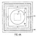
- FIG. 4Ais a plan view of the subassembly of FIG. 2 having one type of heat sink assembly used in the integrated circuit package shown in FIG. 1 ;
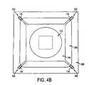
- FIG. 4Bis a plan view of a subassembly of an integrated circuit package having a second type of heat sink capable of being used in the integrated circuit package shown in FIG. 1 ;
- FIG. 5is a plan view of the heat sink shown in the subassembly of FIG. 4A ;
- FIG. 6is a plan view of a heat sink assembly as shown in FIG. 4A , which becomes the heat sink shown in FIG. 5 once assembled into an integrated circuit package such as the embodiment shown in FIG. 1 ;
- FIG. 7is a plan view of a third type of heat sink capable of being used in the integrated circuit package shown in FIG. 1 ;
- FIG. 8is a plan view of a fourth type of heat sink capable of being used in the integrated circuit package shown in FIG. 1 ;
- FIG. 9Ais a plan view of a matrix frame containing a “3 ⁇ 3” matrix of heat sinks of the type shown in FIG. 5 ;
- FIG. 9Bis a plan view of another matrix frame containing a “2 ⁇ 3” matrix of heat sinks of the type shown in FIG. 4B ;
- FIG. 10is a simplified cross-sectional view along line A—A of the heat sink shown in FIG. 5 , and a thermally conductive element of one embodiment;
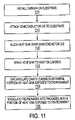
- FIG. 11shows a flowchart of major steps performed in assembly of one embodiment of an integrated circuit package.
- FIG. 1shows certain components of an integrated circuit package according to one embodiment of the present invention displayed in their respective positions relative to one another.
- the integrated circuit package depicted in FIG. 1generally includes a substrate 100 , a heat sink 110 , an adapter assembly 120 , a semiconductor die 130 and an encapsulant 140 .
- a substrate 100 of either a rigid material (e.g., BT, FR4, or ceramic) or a flexible material (e.g., polyimide)has circuit traces 102 onto which a semiconductor die 130 can be interconnected using, for example, wire bonding techniques, direct chip attachment, or tape automated bonding.
- FIG. 1shows a semiconductor die 130 connected to the traces 102 of the substrate 100 via a gold thermo-sonic wire bonding technique.
- gold wires 104interconnect the semiconductor die 130 to the traces of the substrate 100 .
- the semiconductor die 130is connected to the traces 102 via a direct chip attachment technique including solder balls 105 .
- the substrate 100may be produced in strip form to accommodate standard semiconductor manufacturing equipment and process flows, and may also be configured in a matrix format to accommodate high-density packaging.
- the traces 102are embedded photolithographically into the substrate 100 , and are electrically conductive to provide a circuit connection between the semiconductor die 130 and the substrate 100 . Such traces 102 also provide an interconnection between input and output terminals of the semiconductor die 130 and external terminals provided on the package.
- the substrate 100 of the embodiment shown in FIG. 1has a two-layer circuit trace 102 made of copper. A multilayer substrate may also be used in accordance with an embodiment.
- the substrate 100 shown in FIG. 1has several vias drilled into it to connect the top and bottom portions of each circuit trace 102 . Such vias are plated with copper to electrically connect the top and bottom portions of each trace 102 .
- the substrate 100 shown in FIG. 1also has a solder mask 107 on the top and bottom surfaces. The solder mask 107 of one embodiment electrically insulates the substrate and reduces wetting (i.e., reduces wanted flow of solder into the substrate 100 .)
- the external terminals of the package of one embodiment of the present inventioninclude an array of solder balls 106 .
- the solder balls 106function as leads capable of providing power, signal inputs and signal outputs to the semiconductor die 130 .
- Those solder ballsare attached to corresponding traces 102 using a reflow soldering process.
- the solder balls 106can be made of a variety of materials including lead (Pb) free solder.
- Pblead
- Such a configurationmay be referred to as a type of ball grid array. Absent the solder balls 106 , such a configuration may be referred to as a type of LAN grid array.
- the semiconductor die 130may be mounted or attached to the substrate 100 (step 1115 ) with an adhesive material 115 , such as epoxy.
- an adhesive material 115such as epoxy.
- a solder reflow process or other suitable direct chip attachment techniquemay also be used as an alternative way to attach the semiconductor die 130 to the substrate 100 (step 1115 ).
- the heat sink 110is aligned with and positioned above the top surface of the semiconductor die 130 , but not in direct contact with any portion of the semiconductor die 130 .
- the heat sink 110is preferably made of a thermally conductive material such as copper or copper alloy.
- FIG. 2shows, in cross-sectional view, a carrier 200 installed onto the substrate 100 .
- the carrier 200can be mounted on the substrate 100 by mechanical fastening, adhesive joining or other suitable technique (step 1110 ).
- the carrier 200may have one or more recesses 202 sized to accept support structure 114 of a heat sink assembly (step 1125 ).
- the carrier 200is configured to accept either an individual heat sink assembly (as shown in FIGS. 4A and 4B ), or a matrix heat sink assembly 310 containing a number of heat sinks 110 (as shown in FIGS.
- the support structure 114helps to properly align the heat sink 110 during assembly (step 1120 ) and, accordingly, may be removed (as discussed below) in whole or in part prior to completion of an integrated circuit package. In one preferred embodiment, however, some portions of the support structure 114 remain in the final integrated circuit package and are exposed to the ambient environment. For example, in the embodiment depicted in FIG. 1 , portions of the support structure 114 serve as heat dissipation surfaces.
- FIG. 4BFurther details of the heat sink 110 of a subassembly shown in FIG. 4B include extending fingers 116 of the support structure 114 . As shown in plan view by FIG. 4B , the fingers 116 may be sized and shaped to engage matching wells or recesses 202 in the supporting walls of the carrier 200 (step 1125 ). Such fingers 116 in whole or in part support the heat sink 110 prior to encapsulation (step 1130 ) and align the heat sink 110 above the semiconductor die 130 .
- FIGS. 4B , 5 , 7 and 8each show a different geometry for a heat sink 110 .
- the heat sink 110may be sized and configured for use in a specific package arrangement.
- the heat sink 110may be sized for incorporation into a package having only a single semiconductor die 130 (see FIG. 1 ).
- several heat sinks 110may be arranged in a matrix configuration 300 to accommodate the assembly of several packages at once.
- Such a matrix configuration 300is selected to allow each heat sink 110 of the matrix to be aligned with the corresponding semiconductor die 130 and an underlying matrix package substrate 100 .
- a 2 ⁇ 3 and a 3 ⁇ 3 matrix of heat sinks 110 within each matrix heat sink assembly 310are shown in FIGS.
- FIG. 9Ashows a 3 ⁇ 3 matrix of heat sinks 110 , wherein each heat sink 110 has a geometry similar to that of an embodiment shown in FIGS. 4A , 5 and 6 .
- FIG. 9Bshows a 2 ⁇ 3 matrix of heat sinks 110 , wherein each heat sink 110 has a geometry similar to that of an embodiment shown in FIG. 4B .
- the heat sink 110has a raised portion 112 protruding above a primary plane of the heat sink 110 .
- an exposed surface of the raised portion 112may be plated with nickel 116 , and functions as a heat dissipation interface with the ambient environment.
- the nickel plating 116protects the heat sink 110 during environmental testing by resisting oxidation of certain heat sink materials, such as copper.
- the raised portion 112can be formed by removing the surrounding portion of the upper surface of the heat sink 110 , for example, by etching.
- the heat sink 110is also oxide coated to enhance the adhesion between the encapsulant material 140 and the heat sink 110 . The oxide coating may be achieved or applied by chemical reaction.
- the adaptor assembly 120 shown in FIGS. 1 and 2provides a thermal path between the semiconductor die 130 and the heat sink 110 .
- Such an adaptor assembly 120includes an adaptor element 122 made of a thermally conductive material (e.g., alumina (Al 2 O 3 ), aluminum nitride, beryllium oxide (BeO), ceramic material, copper, diamond compound, or metal) appropriate for heat transfer between the semiconductor die 130 and the heat sink 110 .
- the adaptor element 122is shaped as a right rectangular solid, such that its upper and lower faces have dimensions similar to the upper face of the semiconductor die 130 .
- One dimension of the adaptor element 122may be selected to match the area of the upper surface of the semiconductor die 130 .
- the thickness of the adaptor element 122may also be selected to accommodate size variations of the semiconductor die 130 and the heat sink 110 .
- the adaptor assembly 120reduces the thermal resistance of the die-to-sink interface.
- the distance from the upper surface of the semiconductor die 130 to the adaptor element 122is minimized to reduce the thermal resistance between the semiconductor die 130 and the heat sink 110 .
- the adaptor element 122does not directly contact the semiconductor 130 surface.
- the distance between the adaptor element 122 and the semiconductor 130 surfaceis about five (5) mils or less.
- An adhesive layer 119having both high thermal conductivity and deformability to minimize stress, such as an elastomer, may be used to join the adaptor element 122 to the heat sink 110 .
- an adhesive layer 119is electrically and thermally conductive.
- the adaptor assembly 120may also include a polymeric thermal interface 124 between the semiconductor die 130 and the adaptor element 122 to further minimize the thermal resistance of the die-to-sink interface.
- the coefficient of polymeric thermal expansion (CTE) of the thermal interface 124is similar to that of silicon to minimize stress on the semiconductor die 130 .
- a thermal interface 124 portion of the adaptor assembly 120may be attached to the heat sink 110 to reduce the distance from the surface of the semiconductor die 130 to the heat sink 110 .
- the semiconductor die 130 , adaptor assembly 120 and a portion of the heat sink 110are encapsulated to form an integrated circuit package according to one embodiment of the present invention.
- the encapsulant 140may be an epoxy based material applied by, for example, either a liquid molding encapsulation process or a transfer molding technique.
- the encapsulation step 1130occurs after the carrier 200 is attached to the substrate 100 (step 1110 ), and the heat sink 110 is installed in the carrier 200 (step 1125 ). During such an encapsulation step 1130 , the cavity 204 of the carrier 200 is filled with encapsulant 140 .
- Solder balls 106are then attached to the traces 102 of the substrate 100 using a reflow soldering process. After such encapsulation and ball attachment assembly steps, the integrated circuit packages are removed from the strip and singulated into individual units using a saw singulation or punching technique (step 1135 ). Upon completion of these assembly steps, the top portion 112 and some portions of the support structure 114 of the heat sink 110 remain exposed to allow heat transfer and dissipation to the ambient environment of the integrated circuit package (see FIG. 1 ).
Landscapes
- Engineering & Computer Science (AREA)
- Microelectronics & Electronic Packaging (AREA)
- Physics & Mathematics (AREA)
- Condensed Matter Physics & Semiconductors (AREA)
- General Physics & Mathematics (AREA)
- Computer Hardware Design (AREA)
- Power Engineering (AREA)
- Manufacturing & Machinery (AREA)
- Chemical & Material Sciences (AREA)
- Materials Engineering (AREA)
- Cooling Or The Like Of Semiconductors Or Solid State Devices (AREA)
Abstract
Description
Claims (18)
Priority Applications (2)
| Application Number | Priority Date | Filing Date | Title |
|---|---|---|---|
| US10/803,782US7015072B2 (en) | 2001-07-11 | 2004-03-18 | Method of manufacturing an enhanced thermal dissipation integrated circuit package |
| US11/367,708US20060223237A1 (en) | 2001-07-11 | 2006-03-06 | Method of manufacturing enhanced thermal dissipation integrated circuit package |
Applications Claiming Priority (2)
| Application Number | Priority Date | Filing Date | Title |
|---|---|---|---|
| US09/902,878US6734552B2 (en) | 2001-07-11 | 2001-07-11 | Enhanced thermal dissipation integrated circuit package |
| US10/803,782US7015072B2 (en) | 2001-07-11 | 2004-03-18 | Method of manufacturing an enhanced thermal dissipation integrated circuit package |
Related Parent Applications (1)
| Application Number | Title | Priority Date | Filing Date |
|---|---|---|---|
| US09/902,878DivisionUS6734552B2 (en) | 2001-07-11 | 2001-07-11 | Enhanced thermal dissipation integrated circuit package |
Related Child Applications (1)
| Application Number | Title | Priority Date | Filing Date |
|---|---|---|---|
| US11/367,708ContinuationUS20060223237A1 (en) | 2001-07-11 | 2006-03-06 | Method of manufacturing enhanced thermal dissipation integrated circuit package |
Publications (2)
| Publication Number | Publication Date |
|---|---|
| US20050003585A1 US20050003585A1 (en) | 2005-01-06 |
| US7015072B2true US7015072B2 (en) | 2006-03-21 |
Family
ID=33553137
Family Applications (2)
| Application Number | Title | Priority Date | Filing Date |
|---|---|---|---|
| US10/803,782Expired - Fee RelatedUS7015072B2 (en) | 2001-07-11 | 2004-03-18 | Method of manufacturing an enhanced thermal dissipation integrated circuit package |
| US11/367,708AbandonedUS20060223237A1 (en) | 2001-07-11 | 2006-03-06 | Method of manufacturing enhanced thermal dissipation integrated circuit package |
Family Applications After (1)
| Application Number | Title | Priority Date | Filing Date |
|---|---|---|---|
| US11/367,708AbandonedUS20060223237A1 (en) | 2001-07-11 | 2006-03-06 | Method of manufacturing enhanced thermal dissipation integrated circuit package |
Country Status (1)
| Country | Link |
|---|---|
| US (2) | US7015072B2 (en) |
Cited By (30)
| Publication number | Priority date | Publication date | Assignee | Title |
|---|---|---|---|---|
| US20030146509A1 (en)* | 2002-02-01 | 2003-08-07 | Broadcom Corporation | Ball grid array package with separated stiffener layer |
| US20050046015A1 (en)* | 2003-08-28 | 2005-03-03 | St Assembly Test Services Ltd. | Array-molded package heat spreader and fabrication method therefor |
| US20050280139A1 (en)* | 2004-06-21 | 2005-12-22 | Broadcom Corporation | Multipiece apparatus for thermal and electromagnetic interference (EMI) shielding enhancement in die-up array packages and method of making the same |
| US20050280127A1 (en)* | 2004-06-21 | 2005-12-22 | Broadcom Corporation | Apparatus and method for thermal and electromagnetic interference (EMI) shielding enhancement in die-up array packages |
| US20060223237A1 (en)* | 2001-07-11 | 2006-10-05 | Combs Edward G | Method of manufacturing enhanced thermal dissipation integrated circuit package |
| US20070065984A1 (en)* | 2005-09-22 | 2007-03-22 | Lau Daniel K | Thermal enhanced package for block mold assembly |
| US20070090502A1 (en)* | 2005-10-20 | 2007-04-26 | Broadcom Corporation | Methods and apparatus for improved thermal performance and electromagnetic interference (EMI) shielding in leadframe integrated circuit (IC) packages |
| US20070267734A1 (en)* | 2006-05-16 | 2007-11-22 | Broadcom Corporation | No-lead IC packages having integrated heat spreader for electromagnetic interference (EMI) shielding and thermal enhancement |
| US20070273049A1 (en)* | 2006-05-12 | 2007-11-29 | Broadcom Corporation | Interconnect structure and formation for package stacking of molded plastic area array package |
| US20070278632A1 (en)* | 2006-06-01 | 2007-12-06 | Broadcom Corporation | Leadframe IC packages having top and bottom integrated heat spreaders |
| US20070281392A1 (en)* | 2006-06-05 | 2007-12-06 | Carsem (M) Sdn. Bhd. | Multiple row exposed leads for mlp high density packages |
| US20080122070A1 (en)* | 2006-11-24 | 2008-05-29 | Siliconware Precision Industries Co., Ltd. | Heat dissipating semiconductor package and fabrication method therefor |
| US20080188015A1 (en)* | 2006-04-27 | 2008-08-07 | Saruch Sangaunwong | Testing and burn-in using a strip socket |
| US20080211089A1 (en)* | 2007-02-16 | 2008-09-04 | Broadcom Corporation | Interposer for die stacking in semiconductor packages and the method of making the same |
| US20080303124A1 (en)* | 2007-06-08 | 2008-12-11 | Broadcom Corporation | Lead frame-BGA package with enhanced thermal performance and I/O counts |
| US20090042339A1 (en)* | 2007-08-10 | 2009-02-12 | Texas Instruments Incorporated | Packaged integrated circuits and methods to form a packaged integrated circuit |
| US20090085195A1 (en)* | 2007-09-28 | 2009-04-02 | Houle Sabina J | Method of Making Microelectronic Package Using Integrated Heat Spreader Stiffener Panel and Microelectronic Package Formed According to the Method |
| US20090166844A1 (en)* | 2007-12-26 | 2009-07-02 | Xuejiao Hu | Metal cover on flip-chip matrix-array (fcmx) substrate for low cost cpu assembly |
| US20090194868A1 (en)* | 2008-02-01 | 2009-08-06 | National Semiconductor Corporation | Panel level methods and systems for packaging integrated circuits with integrated heat sinks |
| US20100079957A1 (en)* | 2008-09-30 | 2010-04-01 | Houle Sabina J | Underfill process and materials for singulated heat spreader stiffener for thin core panel processing |
| US20100246139A1 (en)* | 2009-03-26 | 2010-09-30 | Kabushiki Kaisha Toyota Jidoshokki | Semiconductor apparatus and heat conductive sheet |
| US20100311208A1 (en)* | 2008-05-22 | 2010-12-09 | Utac Thai Limited | Method and apparatus for no lead semiconductor package |
| US20110012254A1 (en)* | 2009-07-14 | 2011-01-20 | Infineon Technologies North America Corp. | Air Cavity Package with Copper Heat Sink and Ceramic Window Frame |
| US20110278714A1 (en)* | 2010-05-14 | 2011-11-17 | Chipmos Technologies Inc. | Chip package device and manufacturing method thereof |
| US8334764B1 (en) | 2008-12-17 | 2012-12-18 | Utac Thai Limited | Method and apparatus to prevent double semiconductor units in test socket |
| US20130236995A1 (en)* | 2009-05-01 | 2013-09-12 | Vossloh-Schwabe Optoelectronic Gmbh & Co. Kg | Electronic apparatus having an encapsulating layer within and outside of a molded frame overlying a connection arrangement on a circuit board |
| US8581381B2 (en) | 2006-06-20 | 2013-11-12 | Broadcom Corporation | Integrated circuit (IC) package stacking and IC packages formed by same |
| US9190343B1 (en) | 2014-07-16 | 2015-11-17 | Freescale Semiconductor, Inc. | Semiconductor device with tube based heat spreader |
| US20180233571A1 (en)* | 2017-02-15 | 2018-08-16 | Toyota Jidosha Kabushiki Kaisha | Semiconductor device and method of manufacturing the same |
| US11538730B2 (en)* | 2020-06-19 | 2022-12-27 | Azurewave Technologies, Inc. | Chip scale package structure of heat-dissipating type |
Families Citing this family (35)
| Publication number | Priority date | Publication date | Assignee | Title |
|---|---|---|---|---|
| US8492906B2 (en) | 2006-04-28 | 2013-07-23 | Utac Thai Limited | Lead frame ball grid array with traces under die |
| US8487451B2 (en) | 2006-04-28 | 2013-07-16 | Utac Thai Limited | Lead frame land grid array with routing connector trace under unit |
| US8310060B1 (en) | 2006-04-28 | 2012-11-13 | Utac Thai Limited | Lead frame land grid array |
| US8461694B1 (en) | 2006-04-28 | 2013-06-11 | Utac Thai Limited | Lead frame ball grid array with traces under die having interlocking features |
| US8460970B1 (en) | 2006-04-28 | 2013-06-11 | Utac Thai Limited | Lead frame ball grid array with traces under die having interlocking features |
| TWI317998B (en)* | 2006-08-14 | 2009-12-01 | Advanced Semiconductor Eng | Package structure and heat sink module thereof |
| US8125077B2 (en) | 2006-09-26 | 2012-02-28 | Utac Thai Limited | Package with heat transfer |
| US8013437B1 (en) | 2006-09-26 | 2011-09-06 | Utac Thai Limited | Package with heat transfer |
| US9761435B1 (en) | 2006-12-14 | 2017-09-12 | Utac Thai Limited | Flip chip cavity package |
| US9082607B1 (en) | 2006-12-14 | 2015-07-14 | Utac Thai Limited | Molded leadframe substrate semiconductor package |
| US7790512B1 (en) | 2007-11-06 | 2010-09-07 | Utac Thai Limited | Molded leadframe substrate semiconductor package |
| US9947605B2 (en) | 2008-09-04 | 2018-04-17 | UTAC Headquarters Pte. Ltd. | Flip chip cavity package |
| US8263437B2 (en)* | 2008-09-05 | 2012-09-11 | STATS ChiPAC, Ltd. | Semiconductor device and method of forming an IPD over a high-resistivity encapsulant separated from other IPDS and baseband circuit |
| US8354740B2 (en)* | 2008-12-01 | 2013-01-15 | Alpha & Omega Semiconductor, Inc. | Top-side cooled semiconductor package with stacked interconnection plates and method |
| US8569877B2 (en) | 2009-03-12 | 2013-10-29 | Utac Thai Limited | Metallic solderability preservation coating on metal part of semiconductor package to prevent oxide |
| US9449900B2 (en) | 2009-07-23 | 2016-09-20 | UTAC Headquarters Pte. Ltd. | Leadframe feature to minimize flip-chip semiconductor die collapse during flip-chip reflow |
| US8368189B2 (en) | 2009-12-04 | 2013-02-05 | Utac Thai Limited | Auxiliary leadframe member for stabilizing the bond wire process |
| US9355940B1 (en) | 2009-12-04 | 2016-05-31 | Utac Thai Limited | Auxiliary leadframe member for stabilizing the bond wire process |
| US8575732B2 (en) | 2010-03-11 | 2013-11-05 | Utac Thai Limited | Leadframe based multi terminal IC package |
| US8871571B2 (en)* | 2010-04-02 | 2014-10-28 | Utac Thai Limited | Apparatus for and methods of attaching heat slugs to package tops |
| JP2012033559A (en)* | 2010-07-28 | 2012-02-16 | J Devices:Kk | Semiconductor device |
| US9029198B2 (en) | 2012-05-10 | 2015-05-12 | Utac Thai Limited | Methods of manufacturing semiconductor devices including terminals with internal routing interconnections |
| US9449905B2 (en) | 2012-05-10 | 2016-09-20 | Utac Thai Limited | Plated terminals with routing interconnections semiconductor device |
| US9006034B1 (en) | 2012-06-11 | 2015-04-14 | Utac Thai Limited | Post-mold for semiconductor package having exposed traces |
| JP2014063844A (en)* | 2012-09-20 | 2014-04-10 | Sony Corp | Semiconductor device, semiconductor device manufacturing method and electronic apparatus |
| US9559064B2 (en)* | 2013-12-04 | 2017-01-31 | Taiwan Semiconductor Manufacturing Company, Ltd. | Warpage control in package-on-package structures |
| US10242953B1 (en) | 2015-05-27 | 2019-03-26 | Utac Headquarters PTE. Ltd | Semiconductor package with plated metal shielding and a method thereof |
| US10242934B1 (en) | 2014-05-07 | 2019-03-26 | Utac Headquarters Pte Ltd. | Semiconductor package with full plating on contact side surfaces and methods thereof |
| US9917038B1 (en) | 2015-11-10 | 2018-03-13 | Utac Headquarters Pte Ltd | Semiconductor package with multiple molding routing layers and a method of manufacturing the same |
| US10109547B2 (en)* | 2016-01-29 | 2018-10-23 | Taiwan Semiconductor Manufacturing Company, Llc | Semiconductor device and method of manufacture |
| US10276477B1 (en) | 2016-05-20 | 2019-04-30 | UTAC Headquarters Pte. Ltd. | Semiconductor package with multiple stacked leadframes and a method of manufacturing the same |
| US11355419B2 (en)* | 2018-01-11 | 2022-06-07 | Amosense Co., Ltd. | Power semiconductor module |
| US11901308B2 (en)* | 2020-07-21 | 2024-02-13 | UTAC Headquarters Pte. Ltd. | Semiconductor packages with integrated shielding |
| US11676912B2 (en)* | 2020-12-23 | 2023-06-13 | Advanced Semiconductor Engineering, Inc. | Semiconductor device package and method for manufacturing the same |
| US12219690B2 (en)* | 2021-08-31 | 2025-02-04 | Arista Networks, Inc. | Damper system for a lidless integrated circuit |
Citations (108)
| Publication number | Priority date | Publication date | Assignee | Title |
|---|---|---|---|---|
| US3908075A (en) | 1971-11-20 | 1975-09-23 | Ferranti Ltd | Lead frame support for semiconductor devices |
| US3942245A (en) | 1971-11-20 | 1976-03-09 | Ferranti Limited | Related to the manufacture of lead frames and the mounting of semiconductor devices thereon |
| US4501960A (en) | 1981-06-22 | 1985-02-26 | Motorola, Inc. | Micropackage for identification card |
| US4674175A (en) | 1985-04-02 | 1987-06-23 | Eta Sa Fabrique D'ebauches | Process for manufacturing electronic modules for microcircuit cards |
| US4701781A (en) | 1984-07-05 | 1987-10-20 | National Semiconductor Corporation | Pre-testable semiconductor die package |
| US4975765A (en) | 1988-07-22 | 1990-12-04 | Contraves Ag | Highly integrated circuit and method for the production thereof |
| US5023202A (en) | 1989-07-14 | 1991-06-11 | Lsi Logic Corporation | Rigid strip carrier for integrated circuits |
| US5041395A (en) | 1989-04-07 | 1991-08-20 | Sgs-Thomson Microelectronics S.A. | Method of encapsulating an integrated circuit using a punched metal grid attached to a perforated dielectric strip |
| JPH03198368A (en) | 1989-12-26 | 1991-08-29 | Nec Corp | Semiconductor device |
| FR2609841B1 (en) | 1987-01-20 | 1991-10-11 | Toshiba Kk | SEMICONDUCTOR INTEGRATED CIRCUIT DEVICE |
| US5122860A (en) | 1987-08-26 | 1992-06-16 | Matsushita Electric Industrial Co., Ltd. | Integrated circuit device and manufacturing method thereof |
| US5157475A (en) | 1988-07-08 | 1992-10-20 | Oki Electric Industry Co., Ltd. | Semiconductor device having a particular conductive lead structure |
| US5172213A (en)* | 1991-05-23 | 1992-12-15 | At&T Bell Laboratories | Molded circuit package having heat dissipating post |
| US5175612A (en) | 1989-12-19 | 1992-12-29 | Lsi Logic Corporation | Heat sink for semiconductor device assembly |
| US5285105A (en) | 1988-12-07 | 1994-02-08 | Tribotech | Semiconductor die packages having lead support frame |
| US5334857A (en) | 1992-04-06 | 1994-08-02 | Motorola, Inc. | Semiconductor device with test-only contacts and method for making the same |
| US5366933A (en) | 1993-10-13 | 1994-11-22 | Intel Corporation | Method for constructing a dual sided, wire bonded integrated circuit chip package |
| US5420460A (en) | 1993-08-05 | 1995-05-30 | Vlsi Technology, Inc. | Thin cavity down ball grid array package based on wirebond technology |
| US5474957A (en) | 1994-05-09 | 1995-12-12 | Nec Corporation | Process of mounting tape automated bonded semiconductor chip on printed circuit board through bumps |
| US5482898A (en) | 1993-04-12 | 1996-01-09 | Amkor Electronics, Inc. | Method for forming a semiconductor device having a thermal dissipator and electromagnetic shielding |
| US5482736A (en) | 1994-08-04 | 1996-01-09 | Amkor Electronics, Inc. | Method for applying flux to ball grid array package |
| US5556807A (en) | 1992-02-18 | 1996-09-17 | Intel Corporation | Advance multilayer molded plastic package using mesic technology |
| US5596485A (en) | 1995-03-16 | 1997-01-21 | Amkor Electronics, Inc. | Plastic packaged integrated circuit with heat spreader |
| US5596231A (en) | 1991-08-05 | 1997-01-21 | Asat, Limited | High power dissipation plastic encapsulated package for integrated circuit die |
| US5620928A (en) | 1995-05-11 | 1997-04-15 | National Semiconductor Corporation | Ultra thin ball grid array using a flex tape or printed wiring board substrate and method |
| US5650593A (en) | 1994-05-26 | 1997-07-22 | Amkor Electronics, Inc. | Thermally enhanced chip carrier package |
| US5672909A (en) | 1995-02-07 | 1997-09-30 | Amkor Electronics, Inc. | Interdigitated wirebond programmable fixed voltage planes |
| US5672548A (en) | 1994-07-11 | 1997-09-30 | International Business Machines Corporation | Method for attaching heat sinks directly to chip carrier modules using flexible-epoxy |
| US5679978A (en) | 1993-12-06 | 1997-10-21 | Fujitsu Limited | Semiconductor device having resin gate hole through substrate for resin encapsulation |
| US5693572A (en) | 1993-12-20 | 1997-12-02 | Sgs-Thomson Microelectronics, Inc. | Ball grid array integrated circuit package with high thermal conductivity |
| US5708567A (en) | 1995-11-15 | 1998-01-13 | Anam Industrial Co., Ltd. | Ball grid array semiconductor package with ring-type heat sink |
| US5729432A (en) | 1995-07-05 | 1998-03-17 | Anam Industrial Col, Ltd. | Ball grid array semiconductor package with improved heat dissipation and dehumidification effect |
| US5736785A (en) | 1996-12-20 | 1998-04-07 | Industrial Technology Research Institute | Semiconductor package for improving the capability of spreading heat |
| US5789813A (en) | 1996-09-30 | 1998-08-04 | Lsi Logic Corporation | Ball grid array package with inexpensive threaded secure locking mechanism to allow removal of a threaded heat sink therefrom |
| US5796163A (en) | 1997-05-23 | 1998-08-18 | Amkor Technology, Inc. | Solder ball joint |
| US5807768A (en) | 1995-09-04 | 1998-09-15 | Anam Industrial Co., Ltd. | Method for fabricating a heat sink-integrated semiconductor package |
| US5854511A (en)* | 1995-11-17 | 1998-12-29 | Anam Semiconductor, Inc. | Semiconductor package including heat sink with layered conductive plate and non-conductive tape bonding to leads |
| US5867368A (en) | 1997-09-09 | 1999-02-02 | Amkor Technology, Inc. | Mounting for a semiconductor integrated circuit device |
| US5874321A (en) | 1995-01-09 | 1999-02-23 | Integrated Device Technology, Inc. | Package integrated circuit having thermal enhancement and reduced footprint size |
| US5886397A (en) | 1996-09-05 | 1999-03-23 | International Rectifier Corporation | Crushable bead on lead finger side surface to improve moldability |
| US5894108A (en) | 1997-02-11 | 1999-04-13 | National Semiconductor Corporation | Plastic package with exposed die |
| US5900676A (en) | 1996-08-19 | 1999-05-04 | Samsung Electronics Co., Ltd. | Semiconductor device package structure having column leads and a method for production thereof |
| US5940271A (en) | 1997-05-02 | 1999-08-17 | Lsi Logic Corporation | Stiffener with integrated heat sink attachment |
| US5939784A (en) | 1997-09-09 | 1999-08-17 | Amkor Technology, Inc. | Shielded surface acoustical wave package |
| US5949655A (en) | 1997-09-09 | 1999-09-07 | Amkor Technology, Inc. | Mounting having an aperture cover with adhesive locking feature for flip chip optical integrated circuit device |
| US5950074A (en) | 1997-04-18 | 1999-09-07 | Amkor Technology, Inc. | Method of making an integrated circuit package |
| US5962810A (en) | 1997-09-09 | 1999-10-05 | Amkor Technology, Inc. | Integrated circuit package employing a transparent encapsulant |
| US5981314A (en) | 1996-10-31 | 1999-11-09 | Amkor Technology, Inc. | Near chip size integrated circuit package |
| US5982621A (en) | 1998-11-23 | 1999-11-09 | Caesar Technology Inc. | Electronic device cooling arrangement |
| US5986336A (en) | 1996-03-22 | 1999-11-16 | Mitsubishi Denki Kabushiki Kaisha | Semiconductor device including a heat radiation plate |
| US5986340A (en) | 1996-05-02 | 1999-11-16 | National Semiconductor Corporation | Ball grid array package with enhanced thermal and electrical characteristics and electronic device incorporating same |
| US6011304A (en) | 1997-05-05 | 2000-01-04 | Lsi Logic Corporation | Stiffener ring attachment with holes and removable snap-in heat sink or heat spreader/lid |
| US6028354A (en) | 1997-10-14 | 2000-02-22 | Amkor Technology, Inc. | Microelectronic device package having a heat sink structure for increasing the thermal conductivity of the package |
| US6049125A (en) | 1997-12-29 | 2000-04-11 | Micron Technology, Inc. | Semiconductor package with heat sink and method of fabrication |
| US6069023A (en) | 1996-06-28 | 2000-05-30 | International Business Machines Corporation | Attaching heat sinks directly to flip chips and ceramic chip carriers |
| US6081028A (en) | 1994-03-29 | 2000-06-27 | Sun Microsystems, Inc. | Thermal management enhancements for cavity packages |
| US6081029A (en) | 1998-03-12 | 2000-06-27 | Matsushita Electronics Corporation | Resin encapsulated semiconductor device having a reduced thickness and improved reliability |
| US6091603A (en)* | 1999-09-30 | 2000-07-18 | International Business Machines Corporation | Customizable lid for improved thermal performance of modules using flip chips |
| US6092281A (en) | 1998-08-28 | 2000-07-25 | Amkor Technology, Inc. | Electromagnetic interference shield driver and method |
| US6097101A (en) | 1998-01-30 | 2000-08-01 | Shinko Electric Industries Co., Ltd. | Package for semiconductor device having frame-like molded portion and producing method of the same |
| US6104086A (en) | 1997-05-20 | 2000-08-15 | Nec Corporation | Semiconductor device having lead terminals bent in J-shape |
| US6111324A (en) | 1998-02-05 | 2000-08-29 | Asat, Limited | Integrated carrier ring/stiffener and method for manufacturing a flexible integrated circuit package |
| US6117705A (en) | 1997-04-18 | 2000-09-12 | Amkor Technology, Inc. | Method of making integrated circuit package having adhesive bead supporting planar lid above planar substrate |
| US6117193A (en) | 1999-10-20 | 2000-09-12 | Amkor Technology, Inc. | Optical sensor array mounting and alignment |
| US6127724A (en) | 1996-10-31 | 2000-10-03 | Tessera, Inc. | Packaged microelectronic elements with enhanced thermal conduction |
| US6150193A (en) | 1996-10-31 | 2000-11-21 | Amkor Technology, Inc. | RF shielded device |
| US6162849A (en) | 1999-01-11 | 2000-12-19 | Ferro Corporation | Thermally conductive thermoplastic |
| US6163458A (en) | 1999-12-03 | 2000-12-19 | Caesar Technology, Inc. | Heat spreader for ball grid array package |
| US6165612A (en) | 1999-05-14 | 2000-12-26 | The Bergquist Company | Thermally conductive interface layers |
| WO2001000927A1 (en) | 1999-06-24 | 2001-01-04 | Akzo Nobel N.V. | Sizing emulsion |
| US6191360B1 (en) | 1999-04-26 | 2001-02-20 | Advanced Semiconductor Engineering, Inc. | Thermally enhanced BGA package |
| US6196002B1 (en) | 1999-06-24 | 2001-03-06 | Advanced Micro Devices, Inc. | Ball grid array package having thermoelectric cooler |
| US6198163B1 (en) | 1999-10-18 | 2001-03-06 | Amkor Technology, Inc. | Thin leadframe-type semiconductor package having heat sink with recess and exposed surface |
| US6208519B1 (en) | 1999-08-31 | 2001-03-27 | Micron Technology, Inc. | Thermally enhanced semiconductor package |
| US6206997B1 (en) | 1999-02-11 | 2001-03-27 | International Business Machines Corporation | Method for bonding heat sinks to overmolds and device formed thereby |
| US6212070B1 (en) | 1996-07-22 | 2001-04-03 | International Business Machines Corporation | Zero force heat sink |
| US6214644B1 (en) | 2000-06-30 | 2001-04-10 | Amkor Technology, Inc. | Flip-chip micromachine package fabrication method |
| US6219238B1 (en) | 1999-05-10 | 2001-04-17 | International Business Machines Corporation | Structure for removably attaching a heat sink to surface mount packages |
| US6222263B1 (en) | 1999-10-19 | 2001-04-24 | International Business Machines Corporation | Chip assembly with load-bearing lid in thermal contact with the chip |
| US6229200B1 (en) | 1998-06-10 | 2001-05-08 | Asat Limited | Saw-singulated leadless plastic chip carrier |
| US6229702B1 (en) | 1999-06-02 | 2001-05-08 | Advanced Semiconductor Engineering, Inc. | Ball grid array semiconductor package having improved heat dissipation efficiency, overall electrical performance and enhanced bonding capability |
| US6236568B1 (en)* | 1999-03-20 | 2001-05-22 | Siliconware Precision Industries, Co., Ltd. | Heat-dissipating structure for integrated circuit package |
| US6246566B1 (en) | 1999-02-08 | 2001-06-12 | Amkor Technology, Inc. | Electrostatic discharge protection package and method |
| US6258629B1 (en) | 1999-08-09 | 2001-07-10 | Amkor Technology, Inc. | Electronic device package and leadframe and method for making the package |
| US6266197B1 (en) | 1999-12-08 | 2001-07-24 | Amkor Technology, Inc. | Molded window array for image sensor packages |
| US6265771B1 (en)* | 1999-01-27 | 2001-07-24 | International Business Machines Corporation | Dual chip with heat sink |
| US6274927B1 (en) | 1999-06-03 | 2001-08-14 | Amkor Technology, Inc. | Plastic package for an optical integrated circuit device and method of making |
| US6281568B1 (en) | 1998-10-21 | 2001-08-28 | Amkor Technology, Inc. | Plastic integrated circuit device package and leadframe having partially undercut leads and die pad |
| US6281241B1 (en) | 1999-11-30 | 2001-08-28 | Asat Ag Applied Science And Technology | Use of melatonin for the treatment of androgenetic alopecia |
| US6285075B1 (en) | 1998-11-02 | 2001-09-04 | Asat, Limited | Integrated circuit package with bonding planes on a ceramic ring using an adhesive assembly |
| US6291884B1 (en) | 1999-11-09 | 2001-09-18 | Amkor Technology, Inc. | Chip-size semiconductor packages |
| US6294830B1 (en) | 1996-04-18 | 2001-09-25 | Tessera, Inc. | Microelectronic assembly with conductive terminals having an exposed surface through a dielectric layer |
| US6294100B1 (en) | 1998-06-10 | 2001-09-25 | Asat Ltd | Exposed die leadless plastic chip carrier |
| US6326678B1 (en) | 1993-09-03 | 2001-12-04 | Asat, Limited | Molded plastic package with heat sink and enhanced electrical performance |
| US6395578B1 (en) | 1999-05-20 | 2002-05-28 | Amkor Technology, Inc. | Semiconductor package and method for fabricating the same |
| US6396143B1 (en) | 1999-04-30 | 2002-05-28 | Mitsubishi Gas Chemical Company, Inc. | Ball grid array type printed wiring board having exellent heat diffusibility and printed wiring board |
| US20020079570A1 (en) | 2000-12-26 | 2002-06-27 | Siliconware Precision Industries Co., Ltd, | Semiconductor package with heat dissipating element |
| US6429048B1 (en) | 2000-12-05 | 2002-08-06 | Asat Ltd. | Metal foil laminated IC package |
| US6429508B1 (en) | 2000-08-09 | 2002-08-06 | Kostat Semiconductor Co., Ltd. | Semiconductor package having implantable conductive lands and method for manufacturing the same |
| US6433360B1 (en) | 1999-01-15 | 2002-08-13 | Xilinx, Inc. | Structure and method of testing failed or returned die to determine failure location and type |
| US6444498B1 (en)* | 2001-08-08 | 2002-09-03 | Siliconware Precision Industries Co., Ltd | Method of making semiconductor package with heat spreader |
| US6452255B1 (en) | 2000-03-20 | 2002-09-17 | National Semiconductor, Corp. | Low inductance leadless package |
| US6458626B1 (en)* | 2001-08-03 | 2002-10-01 | Siliconware Precision Industries Co., Ltd. | Fabricating method for semiconductor package |
| US6498099B1 (en) | 1998-06-10 | 2002-12-24 | Asat Ltd. | Leadless plastic chip carrier with etch back pad singulation |
| US6507102B2 (en) | 1999-05-12 | 2003-01-14 | Amkor Technology, Inc. | Printed circuit board with integral heat sink for semiconductor package |
| US6552417B2 (en) | 1993-09-03 | 2003-04-22 | Asat, Limited | Molded plastic package with heat sink and enhanced electrical performance |
| US6566740B2 (en) | 2000-03-23 | 2003-05-20 | Mitsui High-Tec, Inc. | Lead frame for a semiconductor device and method of manufacturing a semiconductor device |
| US6734552B2 (en)* | 2001-07-11 | 2004-05-11 | Asat Limited | Enhanced thermal dissipation integrated circuit package |
Family Cites Families (7)
| Publication number | Priority date | Publication date | Assignee | Title |
|---|---|---|---|---|
| US4323914A (en)* | 1979-02-01 | 1982-04-06 | International Business Machines Corporation | Heat transfer structure for integrated circuit package |
| US5909056A (en)* | 1997-06-03 | 1999-06-01 | Lsi Logic Corporation | High performance heat spreader for flip chip packages |
| JP2991172B2 (en)* | 1997-10-24 | 1999-12-20 | 日本電気株式会社 | Semiconductor device |
| JP2001044310A (en)* | 1999-07-28 | 2001-02-16 | Mitsubishi Electric Corp | Semiconductor device and mounting method thereof |
| JP2002270717A (en)* | 2001-03-12 | 2002-09-20 | Rohm Co Ltd | Semiconductor device |
| US7015072B2 (en)* | 2001-07-11 | 2006-03-21 | Asat Limited | Method of manufacturing an enhanced thermal dissipation integrated circuit package |
| US6936919B2 (en)* | 2002-08-21 | 2005-08-30 | Texas Instruments Incorporated | Heatsink-substrate-spacer structure for an integrated-circuit package |
- 2004
- 2004-03-18USUS10/803,782patent/US7015072B2/ennot_activeExpired - Fee Related
- 2006
- 2006-03-06USUS11/367,708patent/US20060223237A1/ennot_activeAbandoned
Patent Citations (113)
| Publication number | Priority date | Publication date | Assignee | Title |
|---|---|---|---|---|
| US3942245A (en) | 1971-11-20 | 1976-03-09 | Ferranti Limited | Related to the manufacture of lead frames and the mounting of semiconductor devices thereon |
| US3908075A (en) | 1971-11-20 | 1975-09-23 | Ferranti Ltd | Lead frame support for semiconductor devices |
| US4501960A (en) | 1981-06-22 | 1985-02-26 | Motorola, Inc. | Micropackage for identification card |
| US4701781A (en) | 1984-07-05 | 1987-10-20 | National Semiconductor Corporation | Pre-testable semiconductor die package |
| US4674175A (en) | 1985-04-02 | 1987-06-23 | Eta Sa Fabrique D'ebauches | Process for manufacturing electronic modules for microcircuit cards |
| FR2609841B1 (en) | 1987-01-20 | 1991-10-11 | Toshiba Kk | SEMICONDUCTOR INTEGRATED CIRCUIT DEVICE |
| US5122860A (en) | 1987-08-26 | 1992-06-16 | Matsushita Electric Industrial Co., Ltd. | Integrated circuit device and manufacturing method thereof |
| US5157475A (en) | 1988-07-08 | 1992-10-20 | Oki Electric Industry Co., Ltd. | Semiconductor device having a particular conductive lead structure |
| US4975765A (en) | 1988-07-22 | 1990-12-04 | Contraves Ag | Highly integrated circuit and method for the production thereof |
| US5285105A (en) | 1988-12-07 | 1994-02-08 | Tribotech | Semiconductor die packages having lead support frame |
| US5041395A (en) | 1989-04-07 | 1991-08-20 | Sgs-Thomson Microelectronics S.A. | Method of encapsulating an integrated circuit using a punched metal grid attached to a perforated dielectric strip |
| US5023202A (en) | 1989-07-14 | 1991-06-11 | Lsi Logic Corporation | Rigid strip carrier for integrated circuits |
| US5175612A (en) | 1989-12-19 | 1992-12-29 | Lsi Logic Corporation | Heat sink for semiconductor device assembly |
| JPH03198368A (en) | 1989-12-26 | 1991-08-29 | Nec Corp | Semiconductor device |
| US5172213A (en)* | 1991-05-23 | 1992-12-15 | At&T Bell Laboratories | Molded circuit package having heat dissipating post |
| US5596231A (en) | 1991-08-05 | 1997-01-21 | Asat, Limited | High power dissipation plastic encapsulated package for integrated circuit die |
| US5556807A (en) | 1992-02-18 | 1996-09-17 | Intel Corporation | Advance multilayer molded plastic package using mesic technology |
| US5334857A (en) | 1992-04-06 | 1994-08-02 | Motorola, Inc. | Semiconductor device with test-only contacts and method for making the same |
| US5485037A (en) | 1993-04-12 | 1996-01-16 | Amkor Electronics, Inc. | Semiconductor device having a thermal dissipator and electromagnetic shielding |
| US5482898A (en) | 1993-04-12 | 1996-01-09 | Amkor Electronics, Inc. | Method for forming a semiconductor device having a thermal dissipator and electromagnetic shielding |
| US5420460A (en) | 1993-08-05 | 1995-05-30 | Vlsi Technology, Inc. | Thin cavity down ball grid array package based on wirebond technology |
| US6326678B1 (en) | 1993-09-03 | 2001-12-04 | Asat, Limited | Molded plastic package with heat sink and enhanced electrical performance |
| US6552417B2 (en) | 1993-09-03 | 2003-04-22 | Asat, Limited | Molded plastic package with heat sink and enhanced electrical performance |
| US5366933A (en) | 1993-10-13 | 1994-11-22 | Intel Corporation | Method for constructing a dual sided, wire bonded integrated circuit chip package |
| US5679978A (en) | 1993-12-06 | 1997-10-21 | Fujitsu Limited | Semiconductor device having resin gate hole through substrate for resin encapsulation |
| US5693572A (en) | 1993-12-20 | 1997-12-02 | Sgs-Thomson Microelectronics, Inc. | Ball grid array integrated circuit package with high thermal conductivity |
| US6081028A (en) | 1994-03-29 | 2000-06-27 | Sun Microsystems, Inc. | Thermal management enhancements for cavity packages |
| US5474957A (en) | 1994-05-09 | 1995-12-12 | Nec Corporation | Process of mounting tape automated bonded semiconductor chip on printed circuit board through bumps |
| US5650593A (en) | 1994-05-26 | 1997-07-22 | Amkor Electronics, Inc. | Thermally enhanced chip carrier package |
| US5672548A (en) | 1994-07-11 | 1997-09-30 | International Business Machines Corporation | Method for attaching heat sinks directly to chip carrier modules using flexible-epoxy |
| US5482736A (en) | 1994-08-04 | 1996-01-09 | Amkor Electronics, Inc. | Method for applying flux to ball grid array package |
| US5874321A (en) | 1995-01-09 | 1999-02-23 | Integrated Device Technology, Inc. | Package integrated circuit having thermal enhancement and reduced footprint size |
| US5672909A (en) | 1995-02-07 | 1997-09-30 | Amkor Electronics, Inc. | Interdigitated wirebond programmable fixed voltage planes |
| US5596485A (en) | 1995-03-16 | 1997-01-21 | Amkor Electronics, Inc. | Plastic packaged integrated circuit with heat spreader |
| US5620928A (en) | 1995-05-11 | 1997-04-15 | National Semiconductor Corporation | Ultra thin ball grid array using a flex tape or printed wiring board substrate and method |
| US5729432A (en) | 1995-07-05 | 1998-03-17 | Anam Industrial Col, Ltd. | Ball grid array semiconductor package with improved heat dissipation and dehumidification effect |
| US5807768A (en) | 1995-09-04 | 1998-09-15 | Anam Industrial Co., Ltd. | Method for fabricating a heat sink-integrated semiconductor package |
| US5708567A (en) | 1995-11-15 | 1998-01-13 | Anam Industrial Co., Ltd. | Ball grid array semiconductor package with ring-type heat sink |
| US5854511A (en)* | 1995-11-17 | 1998-12-29 | Anam Semiconductor, Inc. | Semiconductor package including heat sink with layered conductive plate and non-conductive tape bonding to leads |
| US5986336A (en) | 1996-03-22 | 1999-11-16 | Mitsubishi Denki Kabushiki Kaisha | Semiconductor device including a heat radiation plate |
| US6294830B1 (en) | 1996-04-18 | 2001-09-25 | Tessera, Inc. | Microelectronic assembly with conductive terminals having an exposed surface through a dielectric layer |
| US5986340A (en) | 1996-05-02 | 1999-11-16 | National Semiconductor Corporation | Ball grid array package with enhanced thermal and electrical characteristics and electronic device incorporating same |
| US6069023A (en) | 1996-06-28 | 2000-05-30 | International Business Machines Corporation | Attaching heat sinks directly to flip chips and ceramic chip carriers |
| US6212070B1 (en) | 1996-07-22 | 2001-04-03 | International Business Machines Corporation | Zero force heat sink |
| US5900676A (en) | 1996-08-19 | 1999-05-04 | Samsung Electronics Co., Ltd. | Semiconductor device package structure having column leads and a method for production thereof |
| US5886397A (en) | 1996-09-05 | 1999-03-23 | International Rectifier Corporation | Crushable bead on lead finger side surface to improve moldability |
| US5789813A (en) | 1996-09-30 | 1998-08-04 | Lsi Logic Corporation | Ball grid array package with inexpensive threaded secure locking mechanism to allow removal of a threaded heat sink therefrom |
| US6127724A (en) | 1996-10-31 | 2000-10-03 | Tessera, Inc. | Packaged microelectronic elements with enhanced thermal conduction |
| US6150193A (en) | 1996-10-31 | 2000-11-21 | Amkor Technology, Inc. | RF shielded device |
| US5981314A (en) | 1996-10-31 | 1999-11-09 | Amkor Technology, Inc. | Near chip size integrated circuit package |
| US6228676B1 (en) | 1996-10-31 | 2001-05-08 | Amkor Technology, Inc. | Near chip size integrated circuit package |
| US5736785A (en) | 1996-12-20 | 1998-04-07 | Industrial Technology Research Institute | Semiconductor package for improving the capability of spreading heat |
| US5894108A (en) | 1997-02-11 | 1999-04-13 | National Semiconductor Corporation | Plastic package with exposed die |
| US6117705A (en) | 1997-04-18 | 2000-09-12 | Amkor Technology, Inc. | Method of making integrated circuit package having adhesive bead supporting planar lid above planar substrate |
| US6034429A (en) | 1997-04-18 | 2000-03-07 | Amkor Technology, Inc. | Integrated circuit package |
| US5950074A (en) | 1997-04-18 | 1999-09-07 | Amkor Technology, Inc. | Method of making an integrated circuit package |
| US5940271A (en) | 1997-05-02 | 1999-08-17 | Lsi Logic Corporation | Stiffener with integrated heat sink attachment |
| US6011304A (en) | 1997-05-05 | 2000-01-04 | Lsi Logic Corporation | Stiffener ring attachment with holes and removable snap-in heat sink or heat spreader/lid |
| US6104086A (en) | 1997-05-20 | 2000-08-15 | Nec Corporation | Semiconductor device having lead terminals bent in J-shape |
| US5796163A (en) | 1997-05-23 | 1998-08-18 | Amkor Technology, Inc. | Solder ball joint |
| US5867368A (en) | 1997-09-09 | 1999-02-02 | Amkor Technology, Inc. | Mounting for a semiconductor integrated circuit device |
| US6143588A (en) | 1997-09-09 | 2000-11-07 | Amkor Technology, Inc. | Method of making an integrated circuit package employing a transparent encapsulant |
| US5962810A (en) | 1997-09-09 | 1999-10-05 | Amkor Technology, Inc. | Integrated circuit package employing a transparent encapsulant |
| US5949655A (en) | 1997-09-09 | 1999-09-07 | Amkor Technology, Inc. | Mounting having an aperture cover with adhesive locking feature for flip chip optical integrated circuit device |
| US5939784A (en) | 1997-09-09 | 1999-08-17 | Amkor Technology, Inc. | Shielded surface acoustical wave package |
| US6028354A (en) | 1997-10-14 | 2000-02-22 | Amkor Technology, Inc. | Microelectronic device package having a heat sink structure for increasing the thermal conductivity of the package |
| US6049125A (en) | 1997-12-29 | 2000-04-11 | Micron Technology, Inc. | Semiconductor package with heat sink and method of fabrication |
| US6097101A (en) | 1998-01-30 | 2000-08-01 | Shinko Electric Industries Co., Ltd. | Package for semiconductor device having frame-like molded portion and producing method of the same |
| US6111324A (en) | 1998-02-05 | 2000-08-29 | Asat, Limited | Integrated carrier ring/stiffener and method for manufacturing a flexible integrated circuit package |
| US6081029A (en) | 1998-03-12 | 2000-06-27 | Matsushita Electronics Corporation | Resin encapsulated semiconductor device having a reduced thickness and improved reliability |
| US6498099B1 (en) | 1998-06-10 | 2002-12-24 | Asat Ltd. | Leadless plastic chip carrier with etch back pad singulation |
| US6242281B1 (en) | 1998-06-10 | 2001-06-05 | Asat, Limited | Saw-singulated leadless plastic chip carrier |
| US6294100B1 (en) | 1998-06-10 | 2001-09-25 | Asat Ltd | Exposed die leadless plastic chip carrier |
| US6229200B1 (en) | 1998-06-10 | 2001-05-08 | Asat Limited | Saw-singulated leadless plastic chip carrier |
| US6092281A (en) | 1998-08-28 | 2000-07-25 | Amkor Technology, Inc. | Electromagnetic interference shield driver and method |
| US6281568B1 (en) | 1998-10-21 | 2001-08-28 | Amkor Technology, Inc. | Plastic integrated circuit device package and leadframe having partially undercut leads and die pad |
| US6285075B1 (en) | 1998-11-02 | 2001-09-04 | Asat, Limited | Integrated circuit package with bonding planes on a ceramic ring using an adhesive assembly |
| US5982621A (en) | 1998-11-23 | 1999-11-09 | Caesar Technology Inc. | Electronic device cooling arrangement |
| US6162849A (en) | 1999-01-11 | 2000-12-19 | Ferro Corporation | Thermally conductive thermoplastic |
| US6433360B1 (en) | 1999-01-15 | 2002-08-13 | Xilinx, Inc. | Structure and method of testing failed or returned die to determine failure location and type |
| US6265771B1 (en)* | 1999-01-27 | 2001-07-24 | International Business Machines Corporation | Dual chip with heat sink |
| US6246566B1 (en) | 1999-02-08 | 2001-06-12 | Amkor Technology, Inc. | Electrostatic discharge protection package and method |
| US6206997B1 (en) | 1999-02-11 | 2001-03-27 | International Business Machines Corporation | Method for bonding heat sinks to overmolds and device formed thereby |
| US6236568B1 (en)* | 1999-03-20 | 2001-05-22 | Siliconware Precision Industries, Co., Ltd. | Heat-dissipating structure for integrated circuit package |
| US6191360B1 (en) | 1999-04-26 | 2001-02-20 | Advanced Semiconductor Engineering, Inc. | Thermally enhanced BGA package |
| US6396143B1 (en) | 1999-04-30 | 2002-05-28 | Mitsubishi Gas Chemical Company, Inc. | Ball grid array type printed wiring board having exellent heat diffusibility and printed wiring board |
| US6219238B1 (en) | 1999-05-10 | 2001-04-17 | International Business Machines Corporation | Structure for removably attaching a heat sink to surface mount packages |
| US6507102B2 (en) | 1999-05-12 | 2003-01-14 | Amkor Technology, Inc. | Printed circuit board with integral heat sink for semiconductor package |
| US6165612A (en) | 1999-05-14 | 2000-12-26 | The Bergquist Company | Thermally conductive interface layers |
| US6395578B1 (en) | 1999-05-20 | 2002-05-28 | Amkor Technology, Inc. | Semiconductor package and method for fabricating the same |
| US6229702B1 (en) | 1999-06-02 | 2001-05-08 | Advanced Semiconductor Engineering, Inc. | Ball grid array semiconductor package having improved heat dissipation efficiency, overall electrical performance and enhanced bonding capability |
| US6274927B1 (en) | 1999-06-03 | 2001-08-14 | Amkor Technology, Inc. | Plastic package for an optical integrated circuit device and method of making |
| WO2001000927A1 (en) | 1999-06-24 | 2001-01-04 | Akzo Nobel N.V. | Sizing emulsion |
| US6196002B1 (en) | 1999-06-24 | 2001-03-06 | Advanced Micro Devices, Inc. | Ball grid array package having thermoelectric cooler |
| US6258629B1 (en) | 1999-08-09 | 2001-07-10 | Amkor Technology, Inc. | Electronic device package and leadframe and method for making the package |
| US6208519B1 (en) | 1999-08-31 | 2001-03-27 | Micron Technology, Inc. | Thermally enhanced semiconductor package |
| US6091603A (en)* | 1999-09-30 | 2000-07-18 | International Business Machines Corporation | Customizable lid for improved thermal performance of modules using flip chips |
| US6198163B1 (en) | 1999-10-18 | 2001-03-06 | Amkor Technology, Inc. | Thin leadframe-type semiconductor package having heat sink with recess and exposed surface |
| US6222263B1 (en) | 1999-10-19 | 2001-04-24 | International Business Machines Corporation | Chip assembly with load-bearing lid in thermal contact with the chip |
| US6117193A (en) | 1999-10-20 | 2000-09-12 | Amkor Technology, Inc. | Optical sensor array mounting and alignment |
| US6291884B1 (en) | 1999-11-09 | 2001-09-18 | Amkor Technology, Inc. | Chip-size semiconductor packages |
| US6281241B1 (en) | 1999-11-30 | 2001-08-28 | Asat Ag Applied Science And Technology | Use of melatonin for the treatment of androgenetic alopecia |
| US6163458A (en) | 1999-12-03 | 2000-12-19 | Caesar Technology, Inc. | Heat spreader for ball grid array package |
| US6266197B1 (en) | 1999-12-08 | 2001-07-24 | Amkor Technology, Inc. | Molded window array for image sensor packages |
| US6452255B1 (en) | 2000-03-20 | 2002-09-17 | National Semiconductor, Corp. | Low inductance leadless package |
| US6566740B2 (en) | 2000-03-23 | 2003-05-20 | Mitsui High-Tec, Inc. | Lead frame for a semiconductor device and method of manufacturing a semiconductor device |
| US6214644B1 (en) | 2000-06-30 | 2001-04-10 | Amkor Technology, Inc. | Flip-chip micromachine package fabrication method |
| US6429508B1 (en) | 2000-08-09 | 2002-08-06 | Kostat Semiconductor Co., Ltd. | Semiconductor package having implantable conductive lands and method for manufacturing the same |
| US6429048B1 (en) | 2000-12-05 | 2002-08-06 | Asat Ltd. | Metal foil laminated IC package |
| US20020079570A1 (en) | 2000-12-26 | 2002-06-27 | Siliconware Precision Industries Co., Ltd, | Semiconductor package with heat dissipating element |
| US6734552B2 (en)* | 2001-07-11 | 2004-05-11 | Asat Limited | Enhanced thermal dissipation integrated circuit package |
| US6458626B1 (en)* | 2001-08-03 | 2002-10-01 | Siliconware Precision Industries Co., Ltd. | Fabricating method for semiconductor package |
| US6444498B1 (en)* | 2001-08-08 | 2002-09-03 | Siliconware Precision Industries Co., Ltd | Method of making semiconductor package with heat spreader |
Non-Patent Citations (6)
| Title |
|---|
| English Translation of French Publication No. 2 609 841 (14 pages). |
| English Translation of JP Laid Open Patent Application No. 3-198368 (3 pages). |
| U.S. Appl. No. 10/062,650 filed Jan. 31, 2002 by McLellan et al. |
| U.S. Appl. No. 10/062,896 filed Jan. 31, 2002 by Pedron et al. |
| U.S. Appl. No. 10/104,263 filed Mar. 22, 2002 by Combs et al. |
| U.S. Appl. No. 10/178,372 filed Jun. 24, 2002 by Pedron et al. |
Cited By (54)
| Publication number | Priority date | Publication date | Assignee | Title |
|---|---|---|---|---|
| US20060223237A1 (en)* | 2001-07-11 | 2006-10-05 | Combs Edward G | Method of manufacturing enhanced thermal dissipation integrated circuit package |
| US7550845B2 (en) | 2002-02-01 | 2009-06-23 | Broadcom Corporation | Ball grid array package with separated stiffener layer |
| US20030146509A1 (en)* | 2002-02-01 | 2003-08-07 | Broadcom Corporation | Ball grid array package with separated stiffener layer |
| US20050046015A1 (en)* | 2003-08-28 | 2005-03-03 | St Assembly Test Services Ltd. | Array-molded package heat spreader and fabrication method therefor |
| US7863730B2 (en)* | 2003-08-28 | 2011-01-04 | St Assembly Test Services Ltd. | Array-molded package heat spreader and fabrication method therefor |
| US20050280139A1 (en)* | 2004-06-21 | 2005-12-22 | Broadcom Corporation | Multipiece apparatus for thermal and electromagnetic interference (EMI) shielding enhancement in die-up array packages and method of making the same |
| US20050280127A1 (en)* | 2004-06-21 | 2005-12-22 | Broadcom Corporation | Apparatus and method for thermal and electromagnetic interference (EMI) shielding enhancement in die-up array packages |
| US7432586B2 (en) | 2004-06-21 | 2008-10-07 | Broadcom Corporation | Apparatus and method for thermal and electromagnetic interference (EMI) shielding enhancement in die-up array packages |
| US7791189B2 (en) | 2004-06-21 | 2010-09-07 | Broadcom Corporation | Multipiece apparatus for thermal and electromagnetic interference (EMI) shielding enhancement in die-up array packages and method of making the same |
| US7482686B2 (en)* | 2004-06-21 | 2009-01-27 | Braodcom Corporation | Multipiece apparatus for thermal and electromagnetic interference (EMI) shielding enhancement in die-up array packages and method of making the same |
| US20070065984A1 (en)* | 2005-09-22 | 2007-03-22 | Lau Daniel K | Thermal enhanced package for block mold assembly |
| US20070090502A1 (en)* | 2005-10-20 | 2007-04-26 | Broadcom Corporation | Methods and apparatus for improved thermal performance and electromagnetic interference (EMI) shielding in leadframe integrated circuit (IC) packages |
| US7582951B2 (en) | 2005-10-20 | 2009-09-01 | Broadcom Corporation | Methods and apparatus for improved thermal performance and electromagnetic interference (EMI) shielding in leadframe integrated circuit (IC) packages |
| US7781266B2 (en) | 2005-10-20 | 2010-08-24 | Broadcom Corporation | Methods and apparatus for improved thermal performance and electromagnetic interference (EMI) shielding in leadframe integrated circuit (IC) packages |
| US7696772B2 (en) | 2006-04-27 | 2010-04-13 | Ns Electronics Bangkok Ltd | Strip socket for testing and burn-in having recessed portions with material that extends across a bottom surface of the corresponding semiconductor device |
| US20080211072A1 (en)* | 2006-04-27 | 2008-09-04 | Saruch Sangaunwong | Testing and burn-in using a strip socket |
| US20080188015A1 (en)* | 2006-04-27 | 2008-08-07 | Saruch Sangaunwong | Testing and burn-in using a strip socket |
| US20070273049A1 (en)* | 2006-05-12 | 2007-11-29 | Broadcom Corporation | Interconnect structure and formation for package stacking of molded plastic area array package |
| US7714453B2 (en) | 2006-05-12 | 2010-05-11 | Broadcom Corporation | Interconnect structure and formation for package stacking of molded plastic area array package |
| US8183680B2 (en) | 2006-05-16 | 2012-05-22 | Broadcom Corporation | No-lead IC packages having integrated heat spreader for electromagnetic interference (EMI) shielding and thermal enhancement |
| US20070267734A1 (en)* | 2006-05-16 | 2007-11-22 | Broadcom Corporation | No-lead IC packages having integrated heat spreader for electromagnetic interference (EMI) shielding and thermal enhancement |
| US20070278632A1 (en)* | 2006-06-01 | 2007-12-06 | Broadcom Corporation | Leadframe IC packages having top and bottom integrated heat spreaders |
| US7808087B2 (en) | 2006-06-01 | 2010-10-05 | Broadcom Corporation | Leadframe IC packages having top and bottom integrated heat spreaders |
| US7846774B2 (en)* | 2006-06-05 | 2010-12-07 | Carsem (M) Sdn. Bhd. | Multiple row exposed leads for MLP high density packages |
| US20070281392A1 (en)* | 2006-06-05 | 2007-12-06 | Carsem (M) Sdn. Bhd. | Multiple row exposed leads for mlp high density packages |
| US8581381B2 (en) | 2006-06-20 | 2013-11-12 | Broadcom Corporation | Integrated circuit (IC) package stacking and IC packages formed by same |
| US20080122070A1 (en)* | 2006-11-24 | 2008-05-29 | Siliconware Precision Industries Co., Ltd. | Heat dissipating semiconductor package and fabrication method therefor |
| US8183687B2 (en) | 2007-02-16 | 2012-05-22 | Broadcom Corporation | Interposer for die stacking in semiconductor packages and the method of making the same |
| US20080211089A1 (en)* | 2007-02-16 | 2008-09-04 | Broadcom Corporation | Interposer for die stacking in semiconductor packages and the method of making the same |
| US7872335B2 (en) | 2007-06-08 | 2011-01-18 | Broadcom Corporation | Lead frame-BGA package with enhanced thermal performance and I/O counts |
| US20080303124A1 (en)* | 2007-06-08 | 2008-12-11 | Broadcom Corporation | Lead frame-BGA package with enhanced thermal performance and I/O counts |
| US20090042339A1 (en)* | 2007-08-10 | 2009-02-12 | Texas Instruments Incorporated | Packaged integrated circuits and methods to form a packaged integrated circuit |
| US8067256B2 (en)* | 2007-09-28 | 2011-11-29 | Intel Corporation | Method of making microelectronic package using integrated heat spreader stiffener panel and microelectronic package formed according to the method |
| US20090085195A1 (en)* | 2007-09-28 | 2009-04-02 | Houle Sabina J | Method of Making Microelectronic Package Using Integrated Heat Spreader Stiffener Panel and Microelectronic Package Formed According to the Method |
| US20090166844A1 (en)* | 2007-12-26 | 2009-07-02 | Xuejiao Hu | Metal cover on flip-chip matrix-array (fcmx) substrate for low cost cpu assembly |
| US20090194868A1 (en)* | 2008-02-01 | 2009-08-06 | National Semiconductor Corporation | Panel level methods and systems for packaging integrated circuits with integrated heat sinks |
| US7998791B2 (en)* | 2008-02-01 | 2011-08-16 | National Semiconductor Corporation | Panel level methods and systems for packaging integrated circuits with integrated heat sinks |
| US20100311208A1 (en)* | 2008-05-22 | 2010-12-09 | Utac Thai Limited | Method and apparatus for no lead semiconductor package |
| US8063470B1 (en) | 2008-05-22 | 2011-11-22 | Utac Thai Limited | Method and apparatus for no lead semiconductor package |
| US8071426B2 (en) | 2008-05-22 | 2011-12-06 | Utac Thai Limited | Method and apparatus for no lead semiconductor package |
| US8390112B2 (en)* | 2008-09-30 | 2013-03-05 | Intel Corporation | Underfill process and materials for singulated heat spreader stiffener for thin core panel processing |
| US20100079957A1 (en)* | 2008-09-30 | 2010-04-01 | Houle Sabina J | Underfill process and materials for singulated heat spreader stiffener for thin core panel processing |
| US8334764B1 (en) | 2008-12-17 | 2012-12-18 | Utac Thai Limited | Method and apparatus to prevent double semiconductor units in test socket |
| US20100246139A1 (en)* | 2009-03-26 | 2010-09-30 | Kabushiki Kaisha Toyota Jidoshokki | Semiconductor apparatus and heat conductive sheet |
| US20130236995A1 (en)* | 2009-05-01 | 2013-09-12 | Vossloh-Schwabe Optoelectronic Gmbh & Co. Kg | Electronic apparatus having an encapsulating layer within and outside of a molded frame overlying a connection arrangement on a circuit board |
| US9105819B2 (en)* | 2009-05-01 | 2015-08-11 | Abl Ip Holding Llc | Method for making an electronic apparatus having an encapsulating layer within and outside of a molded frame overlying a connection arrangement on a circuit board |
| US8013429B2 (en)* | 2009-07-14 | 2011-09-06 | Infineon Technologies Ag | Air cavity package with copper heat sink and ceramic window frame |
| US20110012254A1 (en)* | 2009-07-14 | 2011-01-20 | Infineon Technologies North America Corp. | Air Cavity Package with Copper Heat Sink and Ceramic Window Frame |
| US20110278714A1 (en)* | 2010-05-14 | 2011-11-17 | Chipmos Technologies Inc. | Chip package device and manufacturing method thereof |
| US8338938B2 (en)* | 2010-05-14 | 2012-12-25 | Chipmos Technologies Inc. | Chip package device and manufacturing method thereof |
| US9190343B1 (en) | 2014-07-16 | 2015-11-17 | Freescale Semiconductor, Inc. | Semiconductor device with tube based heat spreader |
| US20180233571A1 (en)* | 2017-02-15 | 2018-08-16 | Toyota Jidosha Kabushiki Kaisha | Semiconductor device and method of manufacturing the same |
| US10115798B2 (en)* | 2017-02-15 | 2018-10-30 | Toyota Jidosha Kabushiki Kaisha | Semiconductor device and method of manufacturing the same |
| US11538730B2 (en)* | 2020-06-19 | 2022-12-27 | Azurewave Technologies, Inc. | Chip scale package structure of heat-dissipating type |
Also Published As
| Publication number | Publication date |
|---|---|
| US20050003585A1 (en) | 2005-01-06 |
| US20060223237A1 (en) | 2006-10-05 |
Similar Documents
| Publication | Publication Date | Title |
|---|---|---|
| US7015072B2 (en) | Method of manufacturing an enhanced thermal dissipation integrated circuit package | |
| US6734552B2 (en) | Enhanced thermal dissipation integrated circuit package | |
| US20040046241A1 (en) | Method of manufacturing enhanced thermal dissipation integrated circuit package | |
| US6790710B2 (en) | Method of manufacturing an integrated circuit package | |
| US7205674B2 (en) | Semiconductor package with build-up layers formed on chip and fabrication method of the semiconductor package | |
| US6060778A (en) | Ball grid array package | |
| US5843808A (en) | Structure and method for automated assembly of a tab grid array package | |
| US7364944B2 (en) | Method for fabricating thermally enhanced semiconductor package | |
| US7038311B2 (en) | Thermally enhanced semiconductor package | |
| US6781242B1 (en) | Thin ball grid array package | |
| US7312108B2 (en) | Method for assembling a ball grid array package with two substrates | |
| KR100339044B1 (en) | ball grid array semiconductor package and method for making the same | |
| US7061080B2 (en) | Power module package having improved heat dissipating capability | |
| US5710695A (en) | Leadframe ball grid array package | |
| US6544812B1 (en) | Single unit automated assembly of flex enhanced ball grid array packages | |
| US7692276B2 (en) | Thermally enhanced ball grid array package formed in strip with one-piece die-attached exposed heat spreader | |
| JPH06244231A (en) | Airtight semiconductor device and manufacture thereof | |
| US7002251B2 (en) | Semiconductor device | |
| US6140708A (en) | Chip scale package and method for manufacture thereof | |
| US6373125B1 (en) | Chip scale package with direct attachment of chip to lead frame | |
| US6284566B1 (en) | Chip scale package and method for manufacture thereof | |
| US6339253B1 (en) | Semiconductor package | |
| US20030214019A1 (en) | Packaging system for semiconductor devices | |
| US20060012035A1 (en) | Method of packaging integrated circuits, and integrated circuit packages produced by the method | |
| WO2003017328A2 (en) | Encapsulated integrated circuit package and method of manufacturing an integrated circuit package |
Legal Events
| Date | Code | Title | Description |
|---|---|---|---|
| AS | Assignment | Owner name:ASAT LIMITED, HONG KONG Free format text:ASSIGNMENT OF ASSIGNORS INTEREST;ASSIGNORS:COMBS, EDWARD G.;SHEPPARD, ROBERT P.;PUN, TAI WAI;AND OTHERS;REEL/FRAME:015124/0437;SIGNING DATES FROM 20020403 TO 20020415 | |
| FPAY | Fee payment | Year of fee payment:4 | |
| FEPP | Fee payment procedure | Free format text:PAYER NUMBER DE-ASSIGNED (ORIGINAL EVENT CODE: RMPN); ENTITY STATUS OF PATENT OWNER: LARGE ENTITY Free format text:PAYOR NUMBER ASSIGNED (ORIGINAL EVENT CODE: ASPN); ENTITY STATUS OF PATENT OWNER: LARGE ENTITY | |
| AS | Assignment | Owner name:JPMORGAN CHASE BANK, N.A., AS COLLATERAL AGENT,TEX Free format text:GRANT OF SECURITY INTEREST IN PATENT RIGHTS - FIRST PRIORITY;ASSIGNOR:UTAC HONG KONG LIMITED;REEL/FRAME:024599/0743 Effective date:20100604 Owner name:JPMORGAN CHASE BANK, N.A., AS COLLATERAL AGENT,TEX Free format text:GRANT OF SECURITY INTEREST IN PATENT RIGHTS - SECOND PRIORITY;ASSIGNOR:UTAC HONG KONG LIMITED;REEL/FRAME:024599/0827 Effective date:20100604 Owner name:THE HONGKONG AND SHANGHAI BANKING CORPORATION LIMI Free format text:GRANT OF SECURITY INTEREST IN PATENT RIGHTS - SECOND PRIORITY;ASSIGNOR:UTAC HONG KONG LIMITED;REEL/FRAME:024611/0097 Effective date:20100604 Owner name:JPMORGAN CHASE BANK, N.A., AS COLLATERAL AGENT, TE Free format text:GRANT OF SECURITY INTEREST IN PATENT RIGHTS - FIRST PRIORITY;ASSIGNOR:UTAC HONG KONG LIMITED;REEL/FRAME:024599/0743 Effective date:20100604 Owner name:JPMORGAN CHASE BANK, N.A., AS COLLATERAL AGENT, TE Free format text:GRANT OF SECURITY INTEREST IN PATENT RIGHTS - SECOND PRIORITY;ASSIGNOR:UTAC HONG KONG LIMITED;REEL/FRAME:024599/0827 Effective date:20100604 | |
| AS | Assignment | Owner name:UTAC HONG KONG LIMITED, HONG KONG Free format text:CHANGE OF NAME;ASSIGNOR:ASAT LIMITED;REEL/FRAME:025217/0352 Effective date:20100325 | |
| FPAY | Fee payment | Year of fee payment:8 | |
| AS | Assignment | Owner name:UTAC HEADQUARTERS PTE. LTD., SINGAPORE Free format text:ASSIGNMENT OF ASSIGNORS INTEREST;ASSIGNOR:UTAC HONG KONG LIMITED;REEL/FRAME:037880/0534 Effective date:20150508 | |
| AS | Assignment | Owner name:UTAC HEADQUARTERS PTE. LTD., SINGAPORE Free format text:CORRECTIVE ASSIGNMENT TO CORRECT THE ADD ANNEX INADVERTENTLY LEFT OUT ORIGINAL ASSIGNMENT DOCUMENT PREVIOUSLY RECORDED AT REEL: 037880 FRAME: 0534. ASSIGNOR(S) HEREBY CONFIRMS THE ASSIGNMENT;ASSIGNOR:UTAC HONG KONG LIMITED;REEL/FRAME:039822/0591 Effective date:20150508 | |
| FEPP | Fee payment procedure | Free format text:MAINTENANCE FEE REMINDER MAILED (ORIGINAL EVENT CODE: REM.) | |
| LAPS | Lapse for failure to pay maintenance fees | Free format text:PATENT EXPIRED FOR FAILURE TO PAY MAINTENANCE FEES (ORIGINAL EVENT CODE: EXP.) | |
| STCH | Information on status: patent discontinuation | Free format text:PATENT EXPIRED DUE TO NONPAYMENT OF MAINTENANCE FEES UNDER 37 CFR 1.362 | |
| FP | Lapsed due to failure to pay maintenance fee | Effective date:20180321 |