US7013447B2 - Method for converting a planar transistor design to a vertical double gate transistor design - Google Patents
Method for converting a planar transistor design to a vertical double gate transistor designDownload PDFInfo
- Publication number
- US7013447B2 US7013447B2US10/624,398US62439803AUS7013447B2US 7013447 B2US7013447 B2US 7013447B2US 62439803 AUS62439803 AUS 62439803AUS 7013447 B2US7013447 B2US 7013447B2
- Authority
- US
- United States
- Prior art keywords
- layer
- intermediate layer
- gate
- transistor design
- vertical double
- Prior art date
- Legal status (The legal status is an assumption and is not a legal conclusion. Google has not performed a legal analysis and makes no representation as to the accuracy of the status listed.)
- Expired - Fee Related, expires
Links
Images


Classifications
- H—ELECTRICITY
- H10—SEMICONDUCTOR DEVICES; ELECTRIC SOLID-STATE DEVICES NOT OTHERWISE PROVIDED FOR
- H10D—INORGANIC ELECTRIC SEMICONDUCTOR DEVICES
- H10D30/00—Field-effect transistors [FET]
- H10D30/60—Insulated-gate field-effect transistors [IGFET]
- H10D30/62—Fin field-effect transistors [FinFET]
- H—ELECTRICITY
- H10—SEMICONDUCTOR DEVICES; ELECTRIC SOLID-STATE DEVICES NOT OTHERWISE PROVIDED FOR
- H10D—INORGANIC ELECTRIC SEMICONDUCTOR DEVICES
- H10D84/00—Integrated devices formed in or on semiconductor substrates that comprise only semiconducting layers, e.g. on Si wafers or on GaAs-on-Si wafers
- H10D84/01—Manufacture or treatment
- H10D84/0123—Integrating together multiple components covered by H10D12/00 or H10D30/00, e.g. integrating multiple IGBTs
- H10D84/0126—Integrating together multiple components covered by H10D12/00 or H10D30/00, e.g. integrating multiple IGBTs the components including insulated gates, e.g. IGFETs
- H10D84/0135—Manufacturing their gate conductors
- H—ELECTRICITY
- H10—SEMICONDUCTOR DEVICES; ELECTRIC SOLID-STATE DEVICES NOT OTHERWISE PROVIDED FOR
- H10D—INORGANIC ELECTRIC SEMICONDUCTOR DEVICES
- H10D84/00—Integrated devices formed in or on semiconductor substrates that comprise only semiconducting layers, e.g. on Si wafers or on GaAs-on-Si wafers
- H10D84/01—Manufacture or treatment
- H10D84/02—Manufacture or treatment characterised by using material-based technologies
- H10D84/03—Manufacture or treatment characterised by using material-based technologies using Group IV technology, e.g. silicon technology or silicon-carbide [SiC] technology
- H10D84/038—Manufacture or treatment characterised by using material-based technologies using Group IV technology, e.g. silicon technology or silicon-carbide [SiC] technology using silicon technology, e.g. SiGe
- H—ELECTRICITY
- H10—SEMICONDUCTOR DEVICES; ELECTRIC SOLID-STATE DEVICES NOT OTHERWISE PROVIDED FOR
- H10D—INORGANIC ELECTRIC SEMICONDUCTOR DEVICES
- H10D86/00—Integrated devices formed in or on insulating or conducting substrates, e.g. formed in silicon-on-insulator [SOI] substrates or on stainless steel or glass substrates
- H10D86/201—Integrated devices formed in or on insulating or conducting substrates, e.g. formed in silicon-on-insulator [SOI] substrates or on stainless steel or glass substrates the substrates comprising an insulating layer on a semiconductor body, e.g. SOI
Definitions
- This inventionrelates generally to integrated circuit design, and more particularly, to a method for converting a planar transistor design to a vertical double gate transistor design.
- MOSFETsmetal oxide semiconductor field effect transistors
- the gateis placed between a source and drain electrode and functions to create a channel controlling the amount of current between the source and drain electrodes. Because there is only a single gate electrode to control the channel, the transistor may exhibit undesirable characteristics. For example, the planar transistor may suffer from certain short channel effects, where the drain electrode has an unwanted effect on the channel resulting in excessive leakage current.
- a vertical double gate transistor designalso known as a finFET, has been proposed to eliminate some of the problems with single gate planar transistor design.
- the channelconsists of a pillar or slab, (the fin in finFET) that is oriented perpendicular to the plane of a substrate, but a line connecting the source and drain is parallel to the substrate plane.
- a gate materialsuch as polysilicon or metal is formed on both sides of the fin.
- the double gate arrangementincreases electrostatic coupling between the gates and the channel relative to the single gate design. Also, drive current is improved with decreased leakage. Because of the performance advantages offered by the use of vertical double gate transistors, it would be desirable to convert existing integrated circuit designs that use planar transistors. However, extensive layout/design changes may be necessary when converting a design using planar transistors to a design using vertical double gate transistors. Therefore, there is a need for a way to easily convert a planar transistor design to a vertical double gate transistor design.
- FIGS. 1–6illustrate, in a top down view, a method for converting a planar transistor to a vertical double gate transistor in accordance with the present invention.
- FIGS. 7–8illustrate, in cross sectional views, a portion of a semiconductor device manufactured in accordance with the method of FIGS. 1–6 .
- FIG. 9illustrates a data processing system for running a software implementation of the present invention.
- the present inventionprovides a method for converting a planar transistor design to a vertical double gate transistor design.
- the methodincludes providing a planar transistor layout having a gate layer overlying an active layer.
- a first intermediate layeris defined based on an overlapping region of the gate and active layers, and, using the first intermediate layer, a second intermediate layer is created which defines a spacing between at least two fins of the vertical double gate transistor design.
- the second intermediate layermay also define a length L and a width of the at least two fins.
- One embodimentmodifies a dimension of the first intermediate layer prior to defining the second intermediate layer.
- the methodfurther includes defining a resulting layer based on a non-overlapping region of the second intermediate layer and the active layer. The resulting layer may then be used to create a mask and a semiconductor device corresponding to the vertical double-gate transistor design.
- the methodis implemented as software running on a data processing system.
- FIGS. 1–6illustrate, in a top down view, a method for converting a planar transistor design to a vertical double gate transistor design in accordance with the present invention.
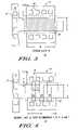
- FIG. 1illustrates a simplified layout 10 of a planar transistor design to be converted to a vertical double gate transistor design in accordance with the present invention.
- the layout 10includes a gate layer 12 overlying an active layer 14 .
- Gate layer 12includes contacts 17 and the active layer 14 includes contacts 16 .
- the number of contacts 16 and 17may be different in other embodiments, and is not important for purposes of describing the invention.
- a channel regionis formed where the gate layer 12 overlies the active layer 14 .
- the channel regionhas a width labeled “W” and a length labeled “L”.
- the word “layer”, as used herein in the discussion of FIGS. 1–6is a set of coordinates representing a polygon in a data processing system. However, in FIGS. 7 and 8 , the word “layer” is also used to describe a material structure in a semiconductor device.
- FIG. 2illustrates a step of performing an AND logical operation of gate layer 12 and active layer 14 to produce an intermediate layer 18 (cross-hatched).
- FIG. 3illustrates a step of over sizing intermediate layer 18 by a value represented by “X” in the horizontal direction and represented by “Y” in the vertical direction.
- the value Ydefines how far a fin extends beyond the gate.
- the value Xmay be adjusted as necessary to correct or optimize spacing considerations and the number of fins.
- FIG. 4illustrates a step of generating another intermediate layer 20 based on the dimensions T, P, W, X, and Y, where T defines a drawn dimension of the silicon fin, P defines the drawn pitch, or distance, between the fins.
- Tdefines a drawn dimension of the silicon fin
- Pdefines the drawn pitch, or distance, between the fins.
- the dimension Pis limited by the minimum pitch of the lithographic process tools (typically 100–200 nanometers).
- the dimension Tis drawn to, for example, 100 nanometers, but with additional processing, such as trimming the silicon or resist, the final value for T may be 20–30 nanometers.
- a length of the intermediate layerwill be at least L+2Y.
- FIG. 5illustrates a step of performing a logical AND operation of intermediate layer 18 and intermediate layer 20 to create layer 22 .
- Layer 22is based on overlapping intermediate layers 18 and 20 and defines spacing between at least two fins of the final vertical double gate transistor design.
- FIG. 6illustrates a step of performing a logical exclusive-or (XOR) operation between active layer 14 and layer 22 to produce a resulting layer 24 .
- the layer 24is used for creating at least a portion of a photo mask used to manufacture a vertical double gate transistor design.
- the layer 22is illustrated in FIG. 6 and corresponds to openings in a resulting photo mask.
- the above stepsproduce a mask that can be used with a positive resist. However, those skilled in the art will realize that the above steps can be modified to produce a mask that is used with a negative resist.
- planar transistor designcan be easily converted to a vertical double gate transistor design.
- the resulting layoutcan be shrunk using transistor scaling techniques or rules.
- FIGS. 7–8illustrate, in cross sectional views through a center region of the fins, a portion of a semiconductor device manufactured in accordance with the method of FIGS. 1–6 .
- FIG. 7illustrates a silicon-on-insulator (SOI) substrate having a silicon substrate 32 , an oxide layer 34 formed thereon, and a silicon layer 36 formed on the oxide layer 34 .
- Photo resist layer 38is patterned using a mask created by performing the method described above with FIGS. 1–6 .
- FIG. 8illustrates the channel region 40 (fins) produced by etching silicon layer 36 ( FIG. 7 ) through the pattern created by photo resist layer 38 .
- Photo resist layer 38is removed.
- a gate stack 42is formed over channel region 40 .
- the gate stack 42comprises gate electrodes and gate dielectrics. Note that the particular process steps for creating the gate stack 42 are not important for describing the invention and can be created a number of ways.
- FIG. 9illustrates, in block diagram form, a general purpose computer 50 in accordance with one embodiment of the present invention which may be used to execute the methods discussed herein.
- General purpose computer 50includes a computer processor 52 and memory 54 coupled by a bus 56 .
- Memory 54may include relatively high speed machine readable media such as DRAM, SRAM, ROM, FLASH, EEPROM, bubble memory, etc.
- Also coupled to bus 56are secondary storage 58 , external storage 60 , output devices such as a monitor 64 , input devices such as a keyboard (with mouse) 66 , and printers 68 .
- Secondary storage 58may include machine readable media such as hard disk drives, magnetic drum, bubble memory, etc.
- External storage 60may include machine readable media such as floppy disks, removable hard drives, magnetic tap, CD-ROM, and even other computers, possibly connected via a communications line. It should be appreciated that there may be overlap between some elements, such as between secondary storage 58 and external storage 60 .
- Executable versions of computer software 62such as, for example, software for performing the layout generation described herein, can be written to, and later read from external storage 60 , loaded for execution directly into memory 54 , or stored on secondary storage 58 prior to loading into memory 54 and execution. Also, the transistor layers may be stored in secondary storage 58 or external storage 60 .
Landscapes
- Thin Film Transistor (AREA)
Abstract
Description
Claims (18)
Priority Applications (1)
| Application Number | Priority Date | Filing Date | Title |
|---|---|---|---|
| US10/624,398US7013447B2 (en) | 2003-07-22 | 2003-07-22 | Method for converting a planar transistor design to a vertical double gate transistor design |
Applications Claiming Priority (1)
| Application Number | Priority Date | Filing Date | Title |
|---|---|---|---|
| US10/624,398US7013447B2 (en) | 2003-07-22 | 2003-07-22 | Method for converting a planar transistor design to a vertical double gate transistor design |
Publications (2)
| Publication Number | Publication Date |
|---|---|
| US20050020015A1 US20050020015A1 (en) | 2005-01-27 |
| US7013447B2true US7013447B2 (en) | 2006-03-14 |
Family
ID=34080003
Family Applications (1)
| Application Number | Title | Priority Date | Filing Date |
|---|---|---|---|
| US10/624,398Expired - Fee RelatedUS7013447B2 (en) | 2003-07-22 | 2003-07-22 | Method for converting a planar transistor design to a vertical double gate transistor design |
Country Status (1)
| Country | Link |
|---|---|
| US (1) | US7013447B2 (en) |
Cited By (25)
| Publication number | Priority date | Publication date | Assignee | Title |
|---|---|---|---|---|
| US20050082522A1 (en)* | 2003-07-25 | 2005-04-21 | Yi-Chun Huang | Strained channel transistor formation |
| US20050136582A1 (en)* | 2003-12-22 | 2005-06-23 | International Business Machines Corporation | Method and device for automated layer generation for double-gate FinFET designs |
| US20060063317A1 (en)* | 2004-09-17 | 2006-03-23 | International Business Machines Corporation | Polysilicon conductor width measurement for 3-dimensional FETs |
| US20070045735A1 (en)* | 2005-08-31 | 2007-03-01 | Orlowski Marius K | FinFET structure with contacts |
| US20070093029A1 (en)* | 2005-10-26 | 2007-04-26 | Freescale Semiconductor, Inc. | Methods of generating planar double gate transistor shapes and data processing system readable media to perform the methods |
| US20070094628A1 (en)* | 2005-10-26 | 2007-04-26 | Freescale Semiconductor, Inc. | Methods of generating planar double gate transistor shapes and data processing system readable media to perform the methods |
| US20070262389A1 (en)* | 2004-01-16 | 2007-11-15 | Robert Chau | Tri-gate transistors and methods to fabricate same |
| US20070264762A1 (en)* | 2003-11-04 | 2007-11-15 | Yee-Chia Yeo | Semiconductor-on-insulator SRAM configured using partially-depleted and fully-depleted transistors |
| US20080263492A1 (en)* | 2007-04-18 | 2008-10-23 | Harry Chuang | 3-Dimensional Device Design Layout |
| US20080258207A1 (en)* | 2005-06-30 | 2008-10-23 | Marko Radosavljevic | Block Contact Architectures for Nanoscale Channel Transistors |
| US20080265290A1 (en)* | 2007-04-24 | 2008-10-30 | Infineon Technologies Ag | Double mesh finfet |
| US20080296691A1 (en)* | 2007-05-30 | 2008-12-04 | Harry Chuang | Layout methods of integrated circuits having unit MOS devices |
| US7989280B2 (en) | 2005-11-30 | 2011-08-02 | Intel Corporation | Dielectric interface for group III-V semiconductor device |
| US8071983B2 (en) | 2005-06-21 | 2011-12-06 | Intel Corporation | Semiconductor device structures and methods of forming semiconductor structures |
| US8084818B2 (en) | 2004-06-30 | 2011-12-27 | Intel Corporation | High mobility tri-gate devices and methods of fabrication |
| US8183646B2 (en) | 2005-02-23 | 2012-05-22 | Intel Corporation | Field effect transistor with narrow bandgap source and drain regions and method of fabrication |
| US8273626B2 (en) | 2003-06-27 | 2012-09-25 | Intel Corporationn | Nonplanar semiconductor device with partially or fully wrapped around gate electrode and methods of fabrication |
| US8294180B2 (en) | 2005-09-28 | 2012-10-23 | Intel Corporation | CMOS devices with a single work function gate electrode and method of fabrication |
| US8362566B2 (en) | 2008-06-23 | 2013-01-29 | Intel Corporation | Stress in trigate devices using complimentary gate fill materials |
| US8502351B2 (en) | 2004-10-25 | 2013-08-06 | Intel Corporation | Nonplanar device with thinned lower body portion and method of fabrication |
| US8617945B2 (en) | 2006-08-02 | 2013-12-31 | Intel Corporation | Stacking fault and twin blocking barrier for integrating III-V on Si |
| US8689154B2 (en)* | 2012-04-13 | 2014-04-01 | Globalfoundries Inc. | Providing timing-closed FinFET designs from planar designs |
| US20140331192A1 (en)* | 2009-12-30 | 2014-11-06 | Taiwan Semiconductor Manufacturing Co., Ltd. | Semiconductor device and method for making the same using semiconductor fin density design rules |
| US9299842B2 (en) | 2012-09-14 | 2016-03-29 | Samsung Electronics Co., Ltd. | Fin transistor and semiconductor integrated circuit including the same |
| US9337307B2 (en) | 2005-06-15 | 2016-05-10 | Intel Corporation | Method for fabricating transistor with thinned channel |
Families Citing this family (9)
| Publication number | Priority date | Publication date | Assignee | Title |
|---|---|---|---|---|
| US7446001B2 (en)* | 2006-02-08 | 2008-11-04 | Freescale Semiconductors, Inc. | Method for forming a semiconductor-on-insulator (SOI) body-contacted device with a portion of drain region removed |
| US7923337B2 (en) | 2007-06-20 | 2011-04-12 | International Business Machines Corporation | Fin field effect transistor devices with self-aligned source and drain regions |
| US8621398B2 (en)* | 2010-05-14 | 2013-12-31 | Taiwan Semiconductor Manufacturing Company, Ltd. | Automatic layout conversion for FinFET device |
| US8881084B2 (en)* | 2010-05-14 | 2014-11-04 | Taiwan Semiconductor Manufacturing Company, Ltd. | FinFET boundary optimization |
| US8799833B2 (en)* | 2011-04-29 | 2014-08-05 | Taiwan Semiconductor Manufacturing Company, Ltd. | System and methods for converting planar design to FinFET design |
| US9177968B1 (en) | 2014-09-19 | 2015-11-03 | Silanna Semiconductor U.S.A., Inc. | Schottky clamped radio frequency switch |
| US20170338215A1 (en)* | 2016-05-20 | 2017-11-23 | Qualcomm Incorporated | Heterogeneous cell array |
| US12206001B2 (en)* | 2019-07-30 | 2025-01-21 | Qualcomm Incorporated | FinFET semiconductor device |
| US11314915B2 (en)* | 2019-09-03 | 2022-04-26 | Samsung Electronics Co., Ltd. | Methods of designing layouts of semiconductor devices |
Citations (7)
| Publication number | Priority date | Publication date | Assignee | Title |
|---|---|---|---|---|
| US6189136B1 (en)* | 1998-07-20 | 2001-02-13 | Philips Electronics, North America Corp. | Design level optical proximity correction methods |
| US6691297B1 (en)* | 1999-03-04 | 2004-02-10 | Matsushita Electric Industrial Co., Ltd. | Method for planning layout for LSI pattern, method for forming LSI pattern and method for generating mask data for LSI |
| US20040117748A1 (en)* | 2002-12-13 | 2004-06-17 | Lsi Logic Corporation | Method for creating derivative integrated circuit layouts for related products |
| US6807662B2 (en)* | 2002-07-09 | 2004-10-19 | Mentor Graphics Corporation | Performance of integrated circuit components via a multiple exposure technique |
| US20040266115A1 (en)* | 2003-06-25 | 2004-12-30 | Bor-Wen Chan | Method of making a gate electrode on a semiconductor device |
| US20050001216A1 (en)* | 2000-10-18 | 2005-01-06 | Adkisson James W. | Method of fabricating semiconductor side wall fin |
| US20050020020A1 (en)* | 2002-07-16 | 2005-01-27 | Nadine Collaert | Integrated semiconductor fin device and a method for manufacturing such device |
Family Cites Families (1)
| Publication number | Priority date | Publication date | Assignee | Title |
|---|---|---|---|---|
| JP4058127B2 (en)* | 1997-02-24 | 2008-03-05 | 富士通株式会社 | Method for changing layout of semiconductor device |
- 2003
- 2003-07-22USUS10/624,398patent/US7013447B2/ennot_activeExpired - Fee Related
Patent Citations (7)
| Publication number | Priority date | Publication date | Assignee | Title |
|---|---|---|---|---|
| US6189136B1 (en)* | 1998-07-20 | 2001-02-13 | Philips Electronics, North America Corp. | Design level optical proximity correction methods |
| US6691297B1 (en)* | 1999-03-04 | 2004-02-10 | Matsushita Electric Industrial Co., Ltd. | Method for planning layout for LSI pattern, method for forming LSI pattern and method for generating mask data for LSI |
| US20050001216A1 (en)* | 2000-10-18 | 2005-01-06 | Adkisson James W. | Method of fabricating semiconductor side wall fin |
| US6807662B2 (en)* | 2002-07-09 | 2004-10-19 | Mentor Graphics Corporation | Performance of integrated circuit components via a multiple exposure technique |
| US20050020020A1 (en)* | 2002-07-16 | 2005-01-27 | Nadine Collaert | Integrated semiconductor fin device and a method for manufacturing such device |
| US20040117748A1 (en)* | 2002-12-13 | 2004-06-17 | Lsi Logic Corporation | Method for creating derivative integrated circuit layouts for related products |
| US20040266115A1 (en)* | 2003-06-25 | 2004-12-30 | Bor-Wen Chan | Method of making a gate electrode on a semiconductor device |
Non-Patent Citations (4)
| Title |
|---|
| Copy of related U.S. Appl. No. 10/074,732. |
| Geppert, "Momentum Builds for Multiple-Gate Transistors," IEEE, Spectrum, pp. 1-3 (2003). |
| Nowak et al., "A Functional FinFET-DGCMOS SRAM Cell," IEEE, 4 pgs., (2002). |
| Ohr, "FinFETs and InP Ics Vie for Dominance in Future Ics," Silicon Strategies, pp. 1-4 (2003). |
Cited By (63)
| Publication number | Priority date | Publication date | Assignee | Title |
|---|---|---|---|---|
| US8273626B2 (en) | 2003-06-27 | 2012-09-25 | Intel Corporationn | Nonplanar semiconductor device with partially or fully wrapped around gate electrode and methods of fabrication |
| US20050082522A1 (en)* | 2003-07-25 | 2005-04-21 | Yi-Chun Huang | Strained channel transistor formation |
| US7867860B2 (en) | 2003-07-25 | 2011-01-11 | Taiwan Semiconductor Manufacturing Company, Ltd. | Strained channel transistor formation |
| US7888201B2 (en)* | 2003-11-04 | 2011-02-15 | Taiwan Semiconductor Manufacturing Company, Ltd. | Semiconductor-on-insulator SRAM configured using partially-depleted and fully-depleted transistors |
| US20070264762A1 (en)* | 2003-11-04 | 2007-11-15 | Yee-Chia Yeo | Semiconductor-on-insulator SRAM configured using partially-depleted and fully-depleted transistors |
| US20050136582A1 (en)* | 2003-12-22 | 2005-06-23 | International Business Machines Corporation | Method and device for automated layer generation for double-gate FinFET designs |
| US7315994B2 (en)* | 2003-12-22 | 2008-01-01 | International Business Machines Corporation | Method and device for automated layer generation for double-gate FinFET designs |
| US20070262389A1 (en)* | 2004-01-16 | 2007-11-15 | Robert Chau | Tri-gate transistors and methods to fabricate same |
| US8084818B2 (en) | 2004-06-30 | 2011-12-27 | Intel Corporation | High mobility tri-gate devices and methods of fabrication |
| US20060063317A1 (en)* | 2004-09-17 | 2006-03-23 | International Business Machines Corporation | Polysilicon conductor width measurement for 3-dimensional FETs |
| US7227183B2 (en)* | 2004-09-17 | 2007-06-05 | International Business Machines Corporation | Polysilicon conductor width measurement for 3-dimensional FETs |
| US20070128740A1 (en)* | 2004-09-17 | 2007-06-07 | International Business Machines Corporation | Polysilicon Conductor Width Measurement for 3-Dimensional FETs |
| US10236356B2 (en) | 2004-10-25 | 2019-03-19 | Intel Corporation | Nonplanar device with thinned lower body portion and method of fabrication |
| US8502351B2 (en) | 2004-10-25 | 2013-08-06 | Intel Corporation | Nonplanar device with thinned lower body portion and method of fabrication |
| US9190518B2 (en) | 2004-10-25 | 2015-11-17 | Intel Corporation | Nonplanar device with thinned lower body portion and method of fabrication |
| US9741809B2 (en) | 2004-10-25 | 2017-08-22 | Intel Corporation | Nonplanar device with thinned lower body portion and method of fabrication |
| US8749026B2 (en) | 2004-10-25 | 2014-06-10 | Intel Corporation | Nonplanar device with thinned lower body portion and method of fabrication |
| US8368135B2 (en) | 2005-02-23 | 2013-02-05 | Intel Corporation | Field effect transistor with narrow bandgap source and drain regions and method of fabrication |
| US8664694B2 (en) | 2005-02-23 | 2014-03-04 | Intel Corporation | Field effect transistor with narrow bandgap source and drain regions and method of fabrication |
| US9368583B2 (en) | 2005-02-23 | 2016-06-14 | Intel Corporation | Field effect transistor with narrow bandgap source and drain regions and method of fabrication |
| US9048314B2 (en) | 2005-02-23 | 2015-06-02 | Intel Corporation | Field effect transistor with narrow bandgap source and drain regions and method of fabrication |
| US9614083B2 (en) | 2005-02-23 | 2017-04-04 | Intel Corporation | Field effect transistor with narrow bandgap source and drain regions and method of fabrication |
| US10121897B2 (en) | 2005-02-23 | 2018-11-06 | Intel Corporation | Field effect transistor with narrow bandgap source and drain regions and method of fabrication |
| US8816394B2 (en) | 2005-02-23 | 2014-08-26 | Intel Corporation | Field effect transistor with narrow bandgap source and drain regions and method of fabrication |
| US8183646B2 (en) | 2005-02-23 | 2012-05-22 | Intel Corporation | Field effect transistor with narrow bandgap source and drain regions and method of fabrication |
| US9748391B2 (en) | 2005-02-23 | 2017-08-29 | Intel Corporation | Field effect transistor with narrow bandgap source and drain regions and method of fabrication |
| US9806195B2 (en) | 2005-06-15 | 2017-10-31 | Intel Corporation | Method for fabricating transistor with thinned channel |
| US9337307B2 (en) | 2005-06-15 | 2016-05-10 | Intel Corporation | Method for fabricating transistor with thinned channel |
| US11978799B2 (en) | 2005-06-15 | 2024-05-07 | Tahoe Research, Ltd. | Method for fabricating transistor with thinned channel |
| US9761724B2 (en) | 2005-06-21 | 2017-09-12 | Intel Corporation | Semiconductor device structures and methods of forming semiconductor structures |
| US8581258B2 (en) | 2005-06-21 | 2013-11-12 | Intel Corporation | Semiconductor device structures and methods of forming semiconductor structures |
| US8071983B2 (en) | 2005-06-21 | 2011-12-06 | Intel Corporation | Semiconductor device structures and methods of forming semiconductor structures |
| US8933458B2 (en) | 2005-06-21 | 2015-01-13 | Intel Corporation | Semiconductor device structures and methods of forming semiconductor structures |
| US9385180B2 (en) | 2005-06-21 | 2016-07-05 | Intel Corporation | Semiconductor device structures and methods of forming semiconductor structures |
| US20080258207A1 (en)* | 2005-06-30 | 2008-10-23 | Marko Radosavljevic | Block Contact Architectures for Nanoscale Channel Transistors |
| US7898041B2 (en)* | 2005-06-30 | 2011-03-01 | Intel Corporation | Block contact architectures for nanoscale channel transistors |
| US7339241B2 (en)* | 2005-08-31 | 2008-03-04 | Freescale Semiconductor, Inc. | FinFET structure with contacts |
| US20070045735A1 (en)* | 2005-08-31 | 2007-03-01 | Orlowski Marius K | FinFET structure with contacts |
| US8294180B2 (en) | 2005-09-28 | 2012-10-23 | Intel Corporation | CMOS devices with a single work function gate electrode and method of fabrication |
| US7530037B2 (en) | 2005-10-26 | 2009-05-05 | Freescale Semiconductor, Inc. | Methods of generating planar double gate transistor shapes and data processing system readable media to perform the methods |
| US7491594B2 (en)* | 2005-10-26 | 2009-02-17 | Freescale Semiconductor, Inc. | Methods of generating planar double gate transistor shapes |
| US20070094628A1 (en)* | 2005-10-26 | 2007-04-26 | Freescale Semiconductor, Inc. | Methods of generating planar double gate transistor shapes and data processing system readable media to perform the methods |
| US20070093029A1 (en)* | 2005-10-26 | 2007-04-26 | Freescale Semiconductor, Inc. | Methods of generating planar double gate transistor shapes and data processing system readable media to perform the methods |
| US7989280B2 (en) | 2005-11-30 | 2011-08-02 | Intel Corporation | Dielectric interface for group III-V semiconductor device |
| US8617945B2 (en) | 2006-08-02 | 2013-12-31 | Intel Corporation | Stacking fault and twin blocking barrier for integrating III-V on Si |
| US8286114B2 (en) | 2007-04-18 | 2012-10-09 | Taiwan Semiconductor Manufacturing Company, Ltd. | 3-dimensional device design layout |
| US20080263492A1 (en)* | 2007-04-18 | 2008-10-23 | Harry Chuang | 3-Dimensional Device Design Layout |
| US7898037B2 (en) | 2007-04-18 | 2011-03-01 | Taiwan Semiconductor Manufacturing Company, Ltd. | Contact scheme for MOSFETs |
| DE102008020140B4 (en)* | 2007-04-24 | 2013-01-17 | Infineon Technologies Ag | Mesh arrangement for field effect transistors and method for their production |
| US20080265290A1 (en)* | 2007-04-24 | 2008-10-30 | Infineon Technologies Ag | Double mesh finfet |
| US7453125B1 (en)* | 2007-04-24 | 2008-11-18 | Infineon Technologies Ag | Double mesh finfet |
| US8803202B2 (en) | 2007-05-30 | 2014-08-12 | Taiwan Semiconductor Manufacturing Company, Ltd. | Layout methods of integrated circuits having unit MOS devices |
| US20080296691A1 (en)* | 2007-05-30 | 2008-12-04 | Harry Chuang | Layout methods of integrated circuits having unit MOS devices |
| US8237201B2 (en) | 2007-05-30 | 2012-08-07 | Taiwan Semiconductor Manufacturing Company, Ltd. | Layout methods of integrated circuits having unit MOS devices |
| US8362566B2 (en) | 2008-06-23 | 2013-01-29 | Intel Corporation | Stress in trigate devices using complimentary gate fill materials |
| US9450092B2 (en) | 2008-06-23 | 2016-09-20 | Intel Corporation | Stress in trigate devices using complimentary gate fill materials |
| US9806193B2 (en) | 2008-06-23 | 2017-10-31 | Intel Corporation | Stress in trigate devices using complimentary gate fill materials |
| US8741733B2 (en) | 2008-06-23 | 2014-06-03 | Intel Corporation | Stress in trigate devices using complimentary gate fill materials |
| US9224754B2 (en) | 2008-06-23 | 2015-12-29 | Intel Corporation | Stress in trigate devices using complimentary gate fill materials |
| US20140331192A1 (en)* | 2009-12-30 | 2014-11-06 | Taiwan Semiconductor Manufacturing Co., Ltd. | Semiconductor device and method for making the same using semiconductor fin density design rules |
| US9245080B2 (en)* | 2009-12-30 | 2016-01-26 | Taiwan Semiconductor Manufacturing Co., Ltd. | Semiconductor device and method for making the same using semiconductor fin density design rules |
| US8689154B2 (en)* | 2012-04-13 | 2014-04-01 | Globalfoundries Inc. | Providing timing-closed FinFET designs from planar designs |
| US9299842B2 (en) | 2012-09-14 | 2016-03-29 | Samsung Electronics Co., Ltd. | Fin transistor and semiconductor integrated circuit including the same |
Also Published As
| Publication number | Publication date |
|---|---|
| US20050020015A1 (en) | 2005-01-27 |
Similar Documents
| Publication | Publication Date | Title |
|---|---|---|
| US7013447B2 (en) | Method for converting a planar transistor design to a vertical double gate transistor design | |
| US8286114B2 (en) | 3-dimensional device design layout | |
| US8099686B2 (en) | CAD flow for 15nm/22nm multiple fine grained wimpy gate lengths in SIT gate flow | |
| US6662350B2 (en) | FinFET layout generation | |
| US8809958B2 (en) | Integrated circuits and methods of design and manufacture thereof | |
| CN110838484B (en) | Integrated circuit including standard cells | |
| CN101740627B (en) | Asymmetric Metal-Oxide-Semiconductor Transistors | |
| US10468420B2 (en) | Method of forming static random-access memory (SRAM) cell array | |
| US20130134513A1 (en) | Finfet with improved gate planarity | |
| US9082875B2 (en) | Methods for normalizing strain in semicondcutor devices and strain normalized semiconductor devices | |
| JPH11260942A (en) | Nonvolatile semiconductor memory device, method of manufacturing the same, and semiconductor integrated circuit device | |
| TW202018787A (en) | Semiconductor device with source and drain contacts of different widths | |
| TW202013223A (en) | Layout of semiconductor device | |
| US9336345B2 (en) | Methods for converting planar designs to FinFET designs in the design and fabrication of integrated circuits | |
| US8484597B2 (en) | Integrated circuit manufacturing method, design method and program | |
| CN112117273A (en) | Integrated circuit device and method of forming the same | |
| TWI745241B (en) | Integrated circuit structure and forming method thereof | |
| TW202139293A (en) | Semiconductor device and manufacturing method thereof | |
| TW202141334A (en) | Semiconductor device | |
| US12142637B2 (en) | Semiconductor device and method of manufacturing the same | |
| CN118829213A (en) | Integrated circuit including a read-only memory cell | |
| KR100680419B1 (en) | Semiconductor device | |
| JPH08321555A (en) | Semiconductor device |
Legal Events
| Date | Code | Title | Description |
|---|---|---|---|
| AS | Assignment | Owner name:MOTOROLA, INC., ILLINOIS Free format text:ASSIGNMENT OF ASSIGNORS INTEREST;ASSIGNORS:MATHEW, LEO;MIN, BYOUNG W.;REEL/FRAME:014328/0630 Effective date:20030722 | |
| AS | Assignment | Owner name:FREESCALE SEMICONDUCTOR, INC., TEXAS Free format text:ASSIGNMENT OF ASSIGNORS INTEREST;ASSIGNOR:MOTOROLA, INC;REEL/FRAME:015360/0718 Effective date:20040404 Owner name:FREESCALE SEMICONDUCTOR, INC.,TEXAS Free format text:ASSIGNMENT OF ASSIGNORS INTEREST;ASSIGNOR:MOTOROLA, INC;REEL/FRAME:015360/0718 Effective date:20040404 | |
| AS | Assignment | Owner name:CITIBANK, N.A. AS COLLATERAL AGENT, NEW YORK Free format text:SECURITY AGREEMENT;ASSIGNORS:FREESCALE SEMICONDUCTOR, INC.;FREESCALE ACQUISITION CORPORATION;FREESCALE ACQUISITION HOLDINGS CORP.;AND OTHERS;REEL/FRAME:018855/0129 Effective date:20061201 Owner name:CITIBANK, N.A. AS COLLATERAL AGENT,NEW YORK Free format text:SECURITY AGREEMENT;ASSIGNORS:FREESCALE SEMICONDUCTOR, INC.;FREESCALE ACQUISITION CORPORATION;FREESCALE ACQUISITION HOLDINGS CORP.;AND OTHERS;REEL/FRAME:018855/0129 Effective date:20061201 | |
| CC | Certificate of correction | ||
| FPAY | Fee payment | Year of fee payment:4 | |
| AS | Assignment | Owner name:CITIBANK, N.A., AS COLLATERAL AGENT,NEW YORK Free format text:SECURITY AGREEMENT;ASSIGNOR:FREESCALE SEMICONDUCTOR, INC.;REEL/FRAME:024397/0001 Effective date:20100413 Owner name:CITIBANK, N.A., AS COLLATERAL AGENT, NEW YORK Free format text:SECURITY AGREEMENT;ASSIGNOR:FREESCALE SEMICONDUCTOR, INC.;REEL/FRAME:024397/0001 Effective date:20100413 | |
| FPAY | Fee payment | Year of fee payment:8 | |
| AS | Assignment | Owner name:CITIBANK, N.A., AS NOTES COLLATERAL AGENT, NEW YORK Free format text:SECURITY AGREEMENT;ASSIGNOR:FREESCALE SEMICONDUCTOR, INC.;REEL/FRAME:030633/0424 Effective date:20130521 Owner name:CITIBANK, N.A., AS NOTES COLLATERAL AGENT, NEW YOR Free format text:SECURITY AGREEMENT;ASSIGNOR:FREESCALE SEMICONDUCTOR, INC.;REEL/FRAME:030633/0424 Effective date:20130521 | |
| AS | Assignment | Owner name:CITIBANK, N.A., AS NOTES COLLATERAL AGENT, NEW YORK Free format text:SECURITY AGREEMENT;ASSIGNOR:FREESCALE SEMICONDUCTOR, INC.;REEL/FRAME:031591/0266 Effective date:20131101 Owner name:CITIBANK, N.A., AS NOTES COLLATERAL AGENT, NEW YOR Free format text:SECURITY AGREEMENT;ASSIGNOR:FREESCALE SEMICONDUCTOR, INC.;REEL/FRAME:031591/0266 Effective date:20131101 | |
| AS | Assignment | Owner name:FREESCALE SEMICONDUCTOR, INC., TEXAS Free format text:PATENT RELEASE;ASSIGNOR:CITIBANK, N.A., AS COLLATERAL AGENT;REEL/FRAME:037354/0225 Effective date:20151207 Owner name:FREESCALE SEMICONDUCTOR, INC., TEXAS Free format text:PATENT RELEASE;ASSIGNOR:CITIBANK, N.A., AS COLLATERAL AGENT;REEL/FRAME:037356/0143 Effective date:20151207 Owner name:FREESCALE SEMICONDUCTOR, INC., TEXAS Free format text:PATENT RELEASE;ASSIGNOR:CITIBANK, N.A., AS COLLATERAL AGENT;REEL/FRAME:037356/0553 Effective date:20151207 | |
| AS | Assignment | Owner name:MORGAN STANLEY SENIOR FUNDING, INC., MARYLAND Free format text:ASSIGNMENT AND ASSUMPTION OF SECURITY INTEREST IN PATENTS;ASSIGNOR:CITIBANK, N.A.;REEL/FRAME:037486/0517 Effective date:20151207 | |
| AS | Assignment | Owner name:MORGAN STANLEY SENIOR FUNDING, INC., MARYLAND Free format text:ASSIGNMENT AND ASSUMPTION OF SECURITY INTEREST IN PATENTS;ASSIGNOR:CITIBANK, N.A.;REEL/FRAME:037518/0292 Effective date:20151207 | |
| AS | Assignment | Owner name:NORTH STAR INNOVATIONS INC., CALIFORNIA Free format text:ASSIGNMENT OF ASSIGNORS INTEREST;ASSIGNOR:FREESCALE SEMICONDUCTOR, INC.;REEL/FRAME:037694/0264 Effective date:20151002 | |
| AS | Assignment | Owner name:NXP, B.V., F/K/A FREESCALE SEMICONDUCTOR, INC., NETHERLANDS Free format text:RELEASE BY SECURED PARTY;ASSIGNOR:MORGAN STANLEY SENIOR FUNDING, INC.;REEL/FRAME:040925/0001 Effective date:20160912 Owner name:NXP, B.V., F/K/A FREESCALE SEMICONDUCTOR, INC., NE Free format text:RELEASE BY SECURED PARTY;ASSIGNOR:MORGAN STANLEY SENIOR FUNDING, INC.;REEL/FRAME:040925/0001 Effective date:20160912 | |
| AS | Assignment | Owner name:NXP B.V., NETHERLANDS Free format text:RELEASE BY SECURED PARTY;ASSIGNOR:MORGAN STANLEY SENIOR FUNDING, INC.;REEL/FRAME:040928/0001 Effective date:20160622 | |
| AS | Assignment | Owner name:MORGAN STANLEY SENIOR FUNDING, INC., MARYLAND Free format text:CORRECTIVE ASSIGNMENT TO CORRECT THE REMOVE PATENTS 8108266 AND 8062324 AND REPLACE THEM WITH 6108266 AND 8060324 PREVIOUSLY RECORDED ON REEL 037518 FRAME 0292. ASSIGNOR(S) HEREBY CONFIRMS THE ASSIGNMENT AND ASSUMPTION OF SECURITY INTEREST IN PATENTS;ASSIGNOR:CITIBANK, N.A.;REEL/FRAME:041703/0536 Effective date:20151207 | |
| AS | Assignment | Owner name:TAIWAN SEMICONDUCTOR MANUFACTURING CO., LTD., TAIW Free format text:ASSIGNMENT OF ASSIGNORS INTEREST;ASSIGNOR:NORTH STAR INNOVATIONS INC.;REEL/FRAME:041717/0736 Effective date:20161006 | |
| FEPP | Fee payment procedure | Free format text:MAINTENANCE FEE REMINDER MAILED (ORIGINAL EVENT CODE: REM.) | |
| LAPS | Lapse for failure to pay maintenance fees | Free format text:PATENT EXPIRED FOR FAILURE TO PAY MAINTENANCE FEES (ORIGINAL EVENT CODE: EXP.) | |
| STCH | Information on status: patent discontinuation | Free format text:PATENT EXPIRED DUE TO NONPAYMENT OF MAINTENANCE FEES UNDER 37 CFR 1.362 | |
| FP | Lapsed due to failure to pay maintenance fee | Effective date:20180314 | |
| AS | Assignment | Owner name:SHENZHEN XINGUODU TECHNOLOGY CO., LTD., CHINA Free format text:CORRECTIVE ASSIGNMENT TO CORRECT THE TO CORRECT THE APPLICATION NO. FROM 13,883,290 TO 13,833,290 PREVIOUSLY RECORDED ON REEL 041703 FRAME 0536. ASSIGNOR(S) HEREBY CONFIRMS THE THE ASSIGNMENT AND ASSUMPTION OF SECURITYINTEREST IN PATENTS.;ASSIGNOR:MORGAN STANLEY SENIOR FUNDING, INC.;REEL/FRAME:048734/0001 Effective date:20190217 | |
| AS | Assignment | Owner name:TAIWAN SEMICONDUCTOR MANUFACTURING CO., LTD., TAIWAN Free format text:323.01(C) ASSIGNMENT OR CHANGE OF NAME IMPROPERLY FILED AND RECORDED BY ANOTHER PERSON AGAINST OWNER'S PATENT;ASSIGNOR:TAIWAN SEMICONDUCTOR MANUFACTURING CO., LTD.;REEL/FRAME:052459/0656 Effective date:20190924 | |
| AS | Assignment | Owner name:MORGAN STANLEY SENIOR FUNDING, INC., MARYLAND Free format text:CORRECTIVE ASSIGNMENT TO CORRECT THE REMOVE APPLICATION11759915 AND REPLACE IT WITH APPLICATION 11759935 PREVIOUSLY RECORDED ON REEL 037486 FRAME 0517. ASSIGNOR(S) HEREBY CONFIRMS THE ASSIGNMENT AND ASSUMPTION OF SECURITYINTEREST IN PATENTS;ASSIGNOR:CITIBANK, N.A.;REEL/FRAME:053547/0421 Effective date:20151207 | |
| AS | Assignment | Owner name:NXP B.V., NETHERLANDS Free format text:CORRECTIVE ASSIGNMENT TO CORRECT THE REMOVEAPPLICATION 11759915 AND REPLACE IT WITH APPLICATION11759935 PREVIOUSLY RECORDED ON REEL 040928 FRAME 0001. ASSIGNOR(S) HEREBY CONFIRMS THE RELEASE OF SECURITYINTEREST;ASSIGNOR:MORGAN STANLEY SENIOR FUNDING, INC.;REEL/FRAME:052915/0001 Effective date:20160622 | |
| AS | Assignment | Owner name:NXP, B.V. F/K/A FREESCALE SEMICONDUCTOR, INC., NETHERLANDS Free format text:CORRECTIVE ASSIGNMENT TO CORRECT THE REMOVEAPPLICATION 11759915 AND REPLACE IT WITH APPLICATION11759935 PREVIOUSLY RECORDED ON REEL 040925 FRAME 0001. ASSIGNOR(S) HEREBY CONFIRMS THE RELEASE OF SECURITYINTEREST;ASSIGNOR:MORGAN STANLEY SENIOR FUNDING, INC.;REEL/FRAME:052917/0001 Effective date:20160912 |