US7012811B1 - Method of tuning a multi-path circuit - Google Patents
Method of tuning a multi-path circuitDownload PDFInfo
- Publication number
- US7012811B1 US7012811B1US09/568,156US56815600AUS7012811B1US 7012811 B1US7012811 B1US 7012811B1US 56815600 AUS56815600 AUS 56815600AUS 7012811 B1US7012811 B1US 7012811B1
- Authority
- US
- United States
- Prior art keywords
- memory module
- circuit board
- signal
- layers
- traces
- Prior art date
- Legal status (The legal status is an assumption and is not a legal conclusion. Google has not performed a legal analysis and makes no representation as to the accuracy of the status listed.)
- Expired - Lifetime
Links
- 238000000034methodMethods0.000titleclaimsabstractdescription35
- 239000000758substrateSubstances0.000claimsdescription18
- XLDBTRJKXLKYTC-UHFFFAOYSA-N2,3,4,4'-tetrachlorobiphenylChemical compoundC1=CC(Cl)=CC=C1C1=CC=C(Cl)C(Cl)=C1ClXLDBTRJKXLKYTC-UHFFFAOYSA-N0.000description6
- 238000005530etchingMethods0.000description6
- 229910052751metalInorganic materials0.000description6
- 239000002184metalSubstances0.000description6
- 238000012360testing methodMethods0.000description6
- 239000004020conductorSubstances0.000description5
- 238000004519manufacturing processMethods0.000description5
- 230000001902propagating effectEffects0.000description4
- 239000011521glassSubstances0.000description3
- PXHVJJICTQNCMI-UHFFFAOYSA-NNickelChemical compound[Ni]PXHVJJICTQNCMI-UHFFFAOYSA-N0.000description2
- PNEYBMLMFCGWSK-UHFFFAOYSA-NAluminaChemical compound[O-2].[O-2].[O-2].[Al+3].[Al+3]PNEYBMLMFCGWSK-UHFFFAOYSA-N0.000description1
- RYGMFSIKBFXOCR-UHFFFAOYSA-NCopperChemical compound[Cu]RYGMFSIKBFXOCR-UHFFFAOYSA-N0.000description1
- 239000004642PolyimideSubstances0.000description1
- 239000004809TeflonSubstances0.000description1
- 229920006362Teflon®Polymers0.000description1
- 239000000654additiveSubstances0.000description1
- 230000000996additive effectEffects0.000description1
- 229910052782aluminiumInorganic materials0.000description1
- XAGFODPZIPBFFR-UHFFFAOYSA-NaluminiumChemical compound[Al]XAGFODPZIPBFFR-UHFFFAOYSA-N0.000description1
- 230000005540biological transmissionEffects0.000description1
- 230000015572biosynthetic processEffects0.000description1
- 229910052802copperInorganic materials0.000description1
- 239000010949copperSubstances0.000description1
- 238000010586diagramMethods0.000description1
- 238000005553drillingMethods0.000description1
- 238000009713electroplatingMethods0.000description1
- 238000005516engineering processMethods0.000description1
- PCHJSUWPFVWCPO-UHFFFAOYSA-NgoldChemical compound[Au]PCHJSUWPFVWCPO-UHFFFAOYSA-N0.000description1
- 229910052737goldInorganic materials0.000description1
- 239000010931goldSubstances0.000description1
- 238000005259measurementMethods0.000description1
- 238000012986modificationMethods0.000description1
- 230000004048modificationEffects0.000description1
- 229910052759nickelInorganic materials0.000description1
- 238000000059patterningMethods0.000description1
- 238000000206photolithographyMethods0.000description1
- 238000007747platingMethods0.000description1
- 229920001721polyimidePolymers0.000description1
- 238000012545processingMethods0.000description1
- 230000000630rising effectEffects0.000description1
- 238000006467substitution reactionMethods0.000description1
Images


Classifications
- H—ELECTRICITY
- H05—ELECTRIC TECHNIQUES NOT OTHERWISE PROVIDED FOR
- H05K—PRINTED CIRCUITS; CASINGS OR CONSTRUCTIONAL DETAILS OF ELECTRIC APPARATUS; MANUFACTURE OF ASSEMBLAGES OF ELECTRICAL COMPONENTS
- H05K1/00—Printed circuits
- H05K1/02—Details
- H05K1/0213—Electrical arrangements not otherwise provided for
- H05K1/0237—High frequency adaptations
- H05K1/0248—Skew reduction or using delay lines
- H—ELECTRICITY
- H05—ELECTRIC TECHNIQUES NOT OTHERWISE PROVIDED FOR
- H05K—PRINTED CIRCUITS; CASINGS OR CONSTRUCTIONAL DETAILS OF ELECTRIC APPARATUS; MANUFACTURE OF ASSEMBLAGES OF ELECTRICAL COMPONENTS
- H05K7/00—Constructional details common to different types of electric apparatus
- H05K7/14—Mounting supporting structure in casing or on frame or rack
- H05K7/1438—Back panels or connecting means therefor; Terminals; Coding means to avoid wrong insertion
- H05K7/1459—Circuit configuration, e.g. routing signals
- H—ELECTRICITY
- H05—ELECTRIC TECHNIQUES NOT OTHERWISE PROVIDED FOR
- H05K—PRINTED CIRCUITS; CASINGS OR CONSTRUCTIONAL DETAILS OF ELECTRIC APPARATUS; MANUFACTURE OF ASSEMBLAGES OF ELECTRICAL COMPONENTS
- H05K2201/00—Indexing scheme relating to printed circuits covered by H05K1/00
- H05K2201/09—Shape and layout
- H05K2201/09209—Shape and layout details of conductors
- H05K2201/09218—Conductive traces
- H05K2201/09263—Meander
- H—ELECTRICITY
- H05—ELECTRIC TECHNIQUES NOT OTHERWISE PROVIDED FOR
- H05K—PRINTED CIRCUITS; CASINGS OR CONSTRUCTIONAL DETAILS OF ELECTRIC APPARATUS; MANUFACTURE OF ASSEMBLAGES OF ELECTRICAL COMPONENTS
- H05K2201/00—Indexing scheme relating to printed circuits covered by H05K1/00
- H05K2201/09—Shape and layout
- H05K2201/09209—Shape and layout details of conductors
- H05K2201/095—Conductive through-holes or vias
- H05K2201/09627—Special connections between adjacent vias, not for grounding vias
- H—ELECTRICITY
- H05—ELECTRIC TECHNIQUES NOT OTHERWISE PROVIDED FOR
- H05K—PRINTED CIRCUITS; CASINGS OR CONSTRUCTIONAL DETAILS OF ELECTRIC APPARATUS; MANUFACTURE OF ASSEMBLAGES OF ELECTRICAL COMPONENTS
- H05K2201/00—Indexing scheme relating to printed circuits covered by H05K1/00
- H05K2201/10—Details of components or other objects attached to or integrated in a printed circuit board
- H05K2201/10007—Types of components
- H05K2201/10159—Memory
Definitions
- the present inventionrelates to the field of printed circuit boards (PCB) and, in particular, to an improved method for reducing timing skew by adjusting the length of signal traces on a printed circuit board.
- PCBprinted circuit boards
- timing skewor signal arrival time
- Many techniqueshave been proposed for handling timing skew, but they all involve substantial costs and/or complex manufacturing techniques.
- U.S. Pat. No. 5,260,892describes a method and apparatus for manufacturing an improved Dynamic Random Access Memory (“DRAM”) electrical signal interconnect structure having special application to Single In-Line Memory Modules (“SIMMs”).
- DRAMDynamic Random Access Memory
- SIMMsSingle In-Line Memory Modules
- the structurecontains an on-board buffer for deriving time-critical signals from a single source.
- the conductor structurefurther includes trace signal routes that allow for approximately equivalent minimum distance signal line lengths.
- the devicefurther includes vias connecting the front and rear surfaces of the SIMMs, resulting in a high speed, high density SIMM with clean rising and falling edges.
- the conduction patternhowever, has to be carefully laid out and is therefore relatively expensive to implement.
- the present inventionprovides an improved method and structure for reducing timing skew for signals, for example clock and/or data signals, that propagate along a printed circuit board, such as a printed circuit board used in a memory module, for example, a DRAM, SRAM, or SDRAM memory module.
- the method of the present inventionadjusts the length of signal traces on the printed circuit board (PCB).
- the signal trace adjustmentis accomplished by tuning the signal path length in both a vertical and a horizontal direction using vias, metal lines and/or conductors in different layers of the printed circuit board. This vertical/horizontal tuning can be used to reduce timing skew of clock and other module signals, thereby increasing module timing margins and performance.
- FIG. 1is a perspective illustration of a portion of a printed circuit board (PCB) containing signal traces prior to skew adjustment.
- PCBprinted circuit board
- FIG. 2is an oscilloscope display showing timing skew measurements.
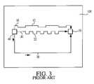
- FIG. 3is a perspective illustration of a portion of a printed circuit board (PCB) containing signal traces after trace length adjustment, in accordance with the prior art.
- PCBprinted circuit board
- FIG. 4is a perspective view of a portion of a printed circuit board (PCB) depicting signal traces after trace length adjustment, and in accordance with a method of the present invention.
- PCBprinted circuit board
- FIG. 5is a cross-sectional view of the printed circuit board (PCB) of FIG. 4 , taken along line 5 — 5 ′.
- PCBprinted circuit board
- FIG. 6is a perspective view of a portion of a multilayer printed circuit board (PCB) depicting signal traces after trace length adjustment, and in accordance with a method of the present invention.
- PCBprinted circuit board
- FIG. 7illustrates a conventional SIMM that uses a printed circuit board constructed according to the present invention.
- FIG. 8is an illustration of a computer system having a memory module with signal traces adjusted according to the present invention.
- the present inventionprovides a method for reducing timing skew for signals propagating along a printed circuit board, for example, along a printed circuit board used as a memory module, such as a DRAM, SRAM, or SDRAM memory module.
- a memory modulesuch as a DRAM, SRAM, or SDRAM memory module.
- the method of the present inventionadjusts the length of signal traces of a printed circuit board (PCB) of the memory module by tuning the signals in both a vertical and a horizontal manner, through vias and metal lines or structures of different multilayers of the module. This vertical/horizontal tuning further reduces timing skew of clock and other module signals, thereby increasing module timing margins and performance.
- PCBprinted circuit board
- FIG. 1illustrates a portion 100 of a conventional memory module printed circuit board (PCB) having a conductor pattern with three signal traces, 10 , 20 , and 30 between a signal origination location 40 and a plurality of signal termination locations 50 a , 50 b , 50 c .
- the origination location 40might be a clock input terminal and the signal terminal locations 50 a , 50 b , 50 c might be clock input terminals of respective integrated circuits which require a clock input signal.
- the signal trace 10 , 20 , and 30have different lengths, with signal trace 20 being the shortest path between the signal origination location 40 and the signal termination location 50 b , and signal trace 30 being the longest path between the signal origination location 40 and the signal termination location 50 c.
- signal arrival timealso called skew
- the time that will take an electrical signal to propagate through trace 30will be longer than the time that will take the same signal to propagate through trace 10 or 20 .
- the time that will take an electrical signal to propagate through trace 10will be longer than the time that will take the same signal to propagate through trace 20 .
- the conductive path lengthmay be altered on the PCB, so that the timing skew can be reduced or even eliminated.
- Time domain transmission techniquesare used in the industry to determine how to adjust the PCB trace length, in particular, how to determine the amount of signal adjustment needed for a particular circuit path.
- in-phase pulsesare launched into a known reference trace, as well as into a PCB trace-under-test.
- Such pulsescan originate from a single pulse source, which may include a signal splitter to produce two identical in-phase pulses.
- FIG. 2illustrates a timing diagram as shown on an oscilloscope connected to an output of a reference trace path (channel 1 ) and a trace path on the PCB (channel 2 ).
- the channel 1 signalrepresents the timing signal received by an oscilloscope traveling through the reference path
- the channel 2 signalrepresents the same timing signal, but passing through the PCB traces 10 , 20 , and 30 , respectively.
- the signal under testwhen the signal that is being measured passes through section 30 , the signal under test best matches the arrival time of the reference signal on channel 1 . However, when the signal under test passes through section 20 , the signal under test arrives much sooner than the reference signal. Likewise, when the signal under test passes through section 10 , the signal under test also arrives sooner than the reference signal.
- the longest trace 30 on the PCBproduces the largest signal delay
- the shortest trace 20produces the shortest signal delay, with the trace 10 falling in between.
- the trace 30is the closest match to providing a signal arrival time that corresponds with the arrival time of the reference signal.
- paths 10 and 20can be lengthened to equal the path length of trace 30 to ensure that signals on all paths arrive at their destinations at substantially the same time.
- the length of the signal tracescan be reduced or increased by adjusting the routing of their corresponding lines, as shown in FIG. 3 .
- the routing adjustmentis done on a horizontal plane of the same layer of the portion 100 of the PCB containing the trace. Because trace 30 is the longest trace of the three traces of FIG. 1 , only traces 10 and 20 must be lengthened, as shown in FIG. 3 . This way, signal path adjustment section 12 (corresponding to signal trace 10 ) and signal path adjustment section 22 (corresponding to signal trace 20 ) minimize or eliminate the timing skew. Electrical signals propagating through any one of the traces 10 , 20 , or 30 will accordingly have substantially equal signal arrival times at the signal termination locations 50 a , 50 b , 50 c.
- the technology employedhas a major drawback, that is the etching of the signal path adjustment sections 12 and 22 with fine spacing.
- signal tracesare extremely small, for example 75 microns wide and 75 microns apart, it is difficult to pattern these fine lines, particularly with available etching techniques.
- the metal conductor patterns which can be produced to adjust path lengthgreatly limit the overall density and reliability of interconnections among various locations on a same level of a PCB.
- the present inventionprovides an improved method for reducing timing skew for signals on a PCB, by tuning the signal paths in both vertical and horizontal planes, as illustrated in FIGS. 4–6 .
- FIG. 4is a perspective view of a portion of a printed circuit board (PCB) 60 that contains a signal path which has been tuned according to the present invention.
- the portion of the PCB 60 depicted in FIG. 4has a top surface 100 and a bottom surface 102 on which a signal trace can be routed.
- the signal tracecan be routed in the X and Y directions on each of the surfaces 100 and 102 , and in the Z direction between surfaces 100 and 102 .
- FIG. 5depicts a cross-sectional view of the portion of the PCB 60 of FIG. 4 , taken along plane 5 — 5 ′.
- FIG. 5depicts the electrically conductive signal path section 12 (corresponding to signal trace 10 of FIG. 3 ) formed on the PCB substrate 60 .
- the signal path section 12consists of horizontal segments 12 a ( FIG. 5 ) formed on the top surface 100 of the PCB substrate 60 , and horizontal segments 12 b formed on the bottom surface 102 of the PCB substrate 60 .
- the horizontal segments 12 a and 12 bare interconnected with vertical segments 12 c .
- the horizontal segments 12 a and 12 bcan propagate in one or both of the X and Y axis directions, while the vertical segments 12 c can propagate in the Z axis direction.
- the PCB substrate 60is typically a PCB laminate, such as FR-4, polyimide/glass, Teflon/glass, or equivalents.
- An inorganic substrate, such as alumina ceramic or glass, for example,may also be used to form the PCB substrate 60 .
- the signal tracesare typically fabricated from copper, nickel, aluminum, gold, or combinations thereof.
- Various methods and techniques for forming signal traces on planar surfacesare known and used in the art.
- a common technique for forming the metal planar patternemploys patterning and etching of signal traces on the substrate by using standard electroplating or additive methods.
- a layer of metaltypically on the order of 2 to 30 microns, is deposited on the PCB substrate 60 , after which this layer is transformed into the signal traces 12 a and 12 b ( FIG. 5 ) by appropriate etching, photolithography or etching steps.
- a plurality of interconnectionsare formed into the PCB substrate 60 to properly interconnect the traces on both surfaces of the substrate.
- a typical method for forming vertical conductive paths, such as signal trace 12 c , between metal layersconsists of first drilling holes into the PCB substrate 60 to form vias, followed by plating interconnections in the vias.
- signal path section 12 of the signal trace 10( FIG. 3 ) consists of both horizontal and vertical structures, which can be designed to have an appropriate path length to minimize signal skews among different circuit paths on the printed circuit board.
- the vertical/horizontal wiring of the signal pathalso affords a greater planar working area, since tuning according to the present invention takes up less of the planar area and more of the vertical area.
- tuning processing stepscould be applied to any or all of the exemplary signal paths 10 , 20 , 30 shown in FIG. 3 .
- the embodiment described aboverefers to only one signal trace routed on a PCB with two surfaces, it is to be understood that the present invention contemplates the use of a plurality of signal traces, each of which may have a path length set by routing the trace in the X, Y axis directions of the surfaces of the board, and vertically in the Z axis direction through the board.
- the present inventionhas been described as using both the signal origination location 40 and the signal termination locations 50 a , 50 b , 50 c on same top planar surface 100 of the PCB 60 , it must be understood that the invention is not limited by the above embodiment, and the origination and termination locations could be situated on different surfaces 100 , 102 of the PCB 60 .
- the present inventionalso contemplates the use of a PCB with a plurality of layers, and, therefore, with a plurality of surfaces on which the signal traces could be routed.
- the portion of a PCB depicted in FIG. 6has three adjacent layers that are defined by a top surface 100 , a bottom surface 106 , and intermediate surfaces 102 and 104 , respectively.
- the signal tracecan be routed in the X and Y directions of each of the surfaces 100 , 102 , 104 , and 106 , and in the Z direction between surfaces 100 , 102 , 104 , and 106 .
- FIG. 6depicts the electrically conductive signal path 12 (corresponding to signal trace 10 of FIG. 3 ), which consists of horizontal segments 12 a , 12 b , 12 d , and 12 f formed on the top surface 100 , the intermediate surfaces 102 and 104 , and on the bottom surface 106 .
- the horizontal segments 12 a , 12 b , 12 d , and 12 fare interconnected with vertical segments 12 c , 12 e , and 12 g .
- the horizontal segments 12 a , 12 b , 12 d , and 12 fcan propagate in one or both of the X and Y axis directions, while the vertical segments 12 c , 12 e , and 12 g can propagate in the Z axis direction.
- the embodiment described aboverefers to a PCB with only three adjacent layers, it must be understood that the present invention is not limited by the above embodiment, and the PCB can consist of any number of adjacent intermediate layers with their corresponding horizontal surfaces, on which signal trace routing could be performed according to the present invention.
- FIG. 7shows a conventional memory module 210 , such as a SIMM or a Multi Chip Module (MCM), for example, that includes PCB substrate 60 and data memory chips 220 .
- An edge connector 230connects a plurality of clock, address and data signals from an external computer to the data memory chips 220 via connecting traces on the PCB substrate 60 and the memory chips 220 are connected themselves in circuit on the PCB 60 .
- the manner in which memory chips 220 are wired on the PCB substrate 60is well known in the art.
- the wiring pattern on the PCB substrate 60contains conductor signal traces for the clock signal having path lengths configured as described above with reference to FIGS. 4–6 .
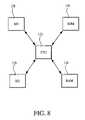
- the method of reducing the timing skew of the present inventionhas particular utility in a memory module used in a computer system, such as the one illustrated in FIG. 8 .
- a processorsuch as a CPU 122
- a computer systemis interconnected with a ROM 134 , RAM 126 , and one or more I/O ports 128 which connect with I/O devices, such as a keyboard, display, mouse, hard drive, or floppy drive.
- the RAM 126may be formed of one or more PCB of a memory module, on which the length of the signal traces has been adjusted in the manner describe above in connection with FIGS. 3–6 . It is also possible to use the invention on a motherboard which mounts the CPU 122 .
- FIG. 2shows the signal traces 10 , 20 , 30 as having a common origination
- the inventionis also equally applicable to signal traces which have respective signal originations, the important aspect of the invention being the use of upper and lower surfaces and vias in a printed circuit board layer to route one or more signal traces in the X, Y directions on both surfaces, and in the Z direction between surfaces, to achieve substantially the same signal path length as other traces to reduce timing skew.
Landscapes
- Engineering & Computer Science (AREA)
- Microelectronics & Electronic Packaging (AREA)
- Computer Networks & Wireless Communication (AREA)
- Dram (AREA)
Abstract
Description
Claims (32)
Priority Applications (1)
| Application Number | Priority Date | Filing Date | Title |
|---|---|---|---|
| US09/568,156US7012811B1 (en) | 2000-05-10 | 2000-05-10 | Method of tuning a multi-path circuit |
Applications Claiming Priority (1)
| Application Number | Priority Date | Filing Date | Title |
|---|---|---|---|
| US09/568,156US7012811B1 (en) | 2000-05-10 | 2000-05-10 | Method of tuning a multi-path circuit |
Publications (1)
| Publication Number | Publication Date |
|---|---|
| US7012811B1true US7012811B1 (en) | 2006-03-14 |
Family
ID=35998825
Family Applications (1)
| Application Number | Title | Priority Date | Filing Date |
|---|---|---|---|
| US09/568,156Expired - LifetimeUS7012811B1 (en) | 2000-05-10 | 2000-05-10 | Method of tuning a multi-path circuit |
Country Status (1)
| Country | Link |
|---|---|
| US (1) | US7012811B1 (en) |
Cited By (11)
| Publication number | Priority date | Publication date | Assignee | Title |
|---|---|---|---|---|
| US20050035816A1 (en)* | 2003-07-09 | 2005-02-17 | Sparling Larry A. | Printed circuit board for a three-phase power device having embedded directional impedance control channels |
| US20070124532A1 (en)* | 2005-04-21 | 2007-05-31 | Bennett Jon C | Interconnection system |
| WO2008051467A1 (en)* | 2006-10-23 | 2008-05-02 | Violin Memory Inc. | Skew management in an interconnection system |
| US7394260B2 (en) | 2006-05-24 | 2008-07-01 | Sun Microsystems, Inc. | Tuning a test trace configured for capacitive coupling to signal traces |
| US20080157385A1 (en)* | 2006-12-29 | 2008-07-03 | Heping Yue | IC package with integral vertical passive delay cells |
| US20090070612A1 (en)* | 2005-04-21 | 2009-03-12 | Maxim Adelman | Memory power management |
| US20090150707A1 (en)* | 2005-04-21 | 2009-06-11 | Drucker Kevin D | Mesosynchronous data bus apparatus and method of data transmission |
| US20090150599A1 (en)* | 2005-04-21 | 2009-06-11 | Bennett Jon C R | Method and system for storage of data in non-volatile media |
| US9286198B2 (en) | 2005-04-21 | 2016-03-15 | Violin Memory | Method and system for storage of data in non-volatile media |
| US9582449B2 (en) | 2005-04-21 | 2017-02-28 | Violin Memory, Inc. | Interconnection system |
| US20220151060A1 (en)* | 2020-11-11 | 2022-05-12 | NGK Electronics Devices, Inc. | Composite wiring board, package, and electronic device |
Citations (25)
| Publication number | Priority date | Publication date | Assignee | Title |
|---|---|---|---|---|
| US4451326A (en) | 1983-09-07 | 1984-05-29 | Advanced Micro Devices, Inc. | Method for interconnecting metallic layers |
| US4734156A (en) | 1985-09-29 | 1988-03-29 | Asahi Chemical Research Laboratory Co., Ltd. | Method for forming electrically conductive circuits on a base board |
| US4743568A (en) | 1987-07-24 | 1988-05-10 | Motorola Inc. | Multilevel interconnect transfer process |
| US4869767A (en) | 1985-05-03 | 1989-09-26 | Hallmark Cards, Incorporated | Process for placing single or multiple patterned layers of conductive material on a substrate |
| US4956694A (en)* | 1988-11-04 | 1990-09-11 | Dense-Pac Microsystems, Inc. | Integrated circuit chip stacking |
| US5055426A (en) | 1990-09-10 | 1991-10-08 | Micron Technology, Inc. | Method for forming a multilevel interconnect structure on a semiconductor wafer |
| US5241456A (en)* | 1990-07-02 | 1993-08-31 | General Electric Company | Compact high density interconnect structure |
| US5260892A (en) | 1991-11-21 | 1993-11-09 | Sun Microsystems, Inc. | High speed electrical signal interconnect structure |
| US5459287A (en)* | 1994-05-18 | 1995-10-17 | Dell Usa, L.P. | Socketed printed circuit board BGA connection apparatus and associated methods |
| US5468995A (en)* | 1994-07-05 | 1995-11-21 | Motorola, Inc. | Semiconductor device having compliant columnar electrical connections |
| US5530288A (en)* | 1994-10-12 | 1996-06-25 | International Business Machines Corporation | Passive interposer including at least one passive electronic component |
| US5763947A (en)* | 1996-01-31 | 1998-06-09 | International Business Machines Corporation | Integrated circuit chip package having configurable contacts and a removable connector |
| US5796746A (en)* | 1995-12-22 | 1998-08-18 | Micron Technology, Inc. | Device and method for testing integrated circuit dice in an integrated circuit module |
| US5838549A (en)* | 1996-01-25 | 1998-11-17 | Hitachi, Ltd. | Memory module and an IC card |
| US5851913A (en) | 1996-06-05 | 1998-12-22 | Advanced Micro Devices, Inc. | Method for forming a multilevel interconnect structure of an integrated circuit by a single via etch and single fill process |
| US5852870A (en) | 1996-04-24 | 1998-12-29 | Amkor Technology, Inc. | Method of making grid array assembly |
| US5937515A (en)* | 1995-04-25 | 1999-08-17 | Johnson; Morgan T. | Reconfigurable circuit fabrication method |
| US5955889A (en)* | 1994-05-20 | 1999-09-21 | Fujitsu Limited | Electronic circuit apparatus for transmitting signals through a bus and semiconductor device for generating a predetermined stable voltage |
| US6051890A (en)* | 1997-12-24 | 2000-04-18 | Intel Corporation | Interleaving a bondwire between two bondwires coupled to a same terminal |
| US6154851A (en)* | 1997-08-05 | 2000-11-28 | Micron Technology, Inc. | Memory repair |
| US6201194B1 (en)* | 1998-12-02 | 2001-03-13 | International Business Machines Corporation | Multi-voltage plane, multi-signal plane circuit card with photoimageable dielectric |
| US6278181B1 (en)* | 1999-06-28 | 2001-08-21 | Advanced Micro Devices, Inc. | Stacked multi-chip modules using C4 interconnect technology having improved thermal management |
| US6366466B1 (en)* | 2000-03-14 | 2002-04-02 | Intel Corporation | Multi-layer printed circuit board with signal traces of varying width |
| US6424034B1 (en)* | 1998-08-31 | 2002-07-23 | Micron Technology, Inc. | High performance packaging for microprocessors and DRAM chips which minimizes timing skews |
| US6661316B2 (en)* | 1999-02-25 | 2003-12-09 | Formfactor, Inc. | High frequency printed circuit board via |
- 2000
- 2000-05-10USUS09/568,156patent/US7012811B1/ennot_activeExpired - Lifetime
Patent Citations (25)
| Publication number | Priority date | Publication date | Assignee | Title |
|---|---|---|---|---|
| US4451326A (en) | 1983-09-07 | 1984-05-29 | Advanced Micro Devices, Inc. | Method for interconnecting metallic layers |
| US4869767A (en) | 1985-05-03 | 1989-09-26 | Hallmark Cards, Incorporated | Process for placing single or multiple patterned layers of conductive material on a substrate |
| US4734156A (en) | 1985-09-29 | 1988-03-29 | Asahi Chemical Research Laboratory Co., Ltd. | Method for forming electrically conductive circuits on a base board |
| US4743568A (en) | 1987-07-24 | 1988-05-10 | Motorola Inc. | Multilevel interconnect transfer process |
| US4956694A (en)* | 1988-11-04 | 1990-09-11 | Dense-Pac Microsystems, Inc. | Integrated circuit chip stacking |
| US5241456A (en)* | 1990-07-02 | 1993-08-31 | General Electric Company | Compact high density interconnect structure |
| US5055426A (en) | 1990-09-10 | 1991-10-08 | Micron Technology, Inc. | Method for forming a multilevel interconnect structure on a semiconductor wafer |
| US5260892A (en) | 1991-11-21 | 1993-11-09 | Sun Microsystems, Inc. | High speed electrical signal interconnect structure |
| US5459287A (en)* | 1994-05-18 | 1995-10-17 | Dell Usa, L.P. | Socketed printed circuit board BGA connection apparatus and associated methods |
| US5955889A (en)* | 1994-05-20 | 1999-09-21 | Fujitsu Limited | Electronic circuit apparatus for transmitting signals through a bus and semiconductor device for generating a predetermined stable voltage |
| US5468995A (en)* | 1994-07-05 | 1995-11-21 | Motorola, Inc. | Semiconductor device having compliant columnar electrical connections |
| US5530288A (en)* | 1994-10-12 | 1996-06-25 | International Business Machines Corporation | Passive interposer including at least one passive electronic component |
| US5937515A (en)* | 1995-04-25 | 1999-08-17 | Johnson; Morgan T. | Reconfigurable circuit fabrication method |
| US5796746A (en)* | 1995-12-22 | 1998-08-18 | Micron Technology, Inc. | Device and method for testing integrated circuit dice in an integrated circuit module |
| US5838549A (en)* | 1996-01-25 | 1998-11-17 | Hitachi, Ltd. | Memory module and an IC card |
| US5763947A (en)* | 1996-01-31 | 1998-06-09 | International Business Machines Corporation | Integrated circuit chip package having configurable contacts and a removable connector |
| US5852870A (en) | 1996-04-24 | 1998-12-29 | Amkor Technology, Inc. | Method of making grid array assembly |
| US5851913A (en) | 1996-06-05 | 1998-12-22 | Advanced Micro Devices, Inc. | Method for forming a multilevel interconnect structure of an integrated circuit by a single via etch and single fill process |
| US6154851A (en)* | 1997-08-05 | 2000-11-28 | Micron Technology, Inc. | Memory repair |
| US6051890A (en)* | 1997-12-24 | 2000-04-18 | Intel Corporation | Interleaving a bondwire between two bondwires coupled to a same terminal |
| US6424034B1 (en)* | 1998-08-31 | 2002-07-23 | Micron Technology, Inc. | High performance packaging for microprocessors and DRAM chips which minimizes timing skews |
| US6201194B1 (en)* | 1998-12-02 | 2001-03-13 | International Business Machines Corporation | Multi-voltage plane, multi-signal plane circuit card with photoimageable dielectric |
| US6661316B2 (en)* | 1999-02-25 | 2003-12-09 | Formfactor, Inc. | High frequency printed circuit board via |
| US6278181B1 (en)* | 1999-06-28 | 2001-08-21 | Advanced Micro Devices, Inc. | Stacked multi-chip modules using C4 interconnect technology having improved thermal management |
| US6366466B1 (en)* | 2000-03-14 | 2002-04-02 | Intel Corporation | Multi-layer printed circuit board with signal traces of varying width |
Cited By (28)
| Publication number | Priority date | Publication date | Assignee | Title |
|---|---|---|---|---|
| US20050035816A1 (en)* | 2003-07-09 | 2005-02-17 | Sparling Larry A. | Printed circuit board for a three-phase power device having embedded directional impedance control channels |
| US7154196B2 (en)* | 2003-07-09 | 2006-12-26 | Motorola, Inc. | Printed circuit board for a three-phase power device having embedded directional impedance control channels |
| US8112655B2 (en) | 2005-04-21 | 2012-02-07 | Violin Memory, Inc. | Mesosynchronous data bus apparatus and method of data transmission |
| US9727263B2 (en) | 2005-04-21 | 2017-08-08 | Violin Memory, Inc. | Method and system for storage of data in a non-volatile media |
| US8452929B2 (en) | 2005-04-21 | 2013-05-28 | Violin Memory Inc. | Method and system for storage of data in non-volatile media |
| US10417159B2 (en) | 2005-04-21 | 2019-09-17 | Violin Systems Llc | Interconnection system |
| US10176861B2 (en) | 2005-04-21 | 2019-01-08 | Violin Systems Llc | RAIDed memory system management |
| US20090070612A1 (en)* | 2005-04-21 | 2009-03-12 | Maxim Adelman | Memory power management |
| US20090150707A1 (en)* | 2005-04-21 | 2009-06-11 | Drucker Kevin D | Mesosynchronous data bus apparatus and method of data transmission |
| US20090150599A1 (en)* | 2005-04-21 | 2009-06-11 | Bennett Jon C R | Method and system for storage of data in non-volatile media |
| US20090216924A1 (en)* | 2005-04-21 | 2009-08-27 | Bennett Jon C R | Interconnection system |
| US20070124532A1 (en)* | 2005-04-21 | 2007-05-31 | Bennett Jon C | Interconnection system |
| US8726064B2 (en) | 2005-04-21 | 2014-05-13 | Violin Memory Inc. | Interconnection system |
| US9384818B2 (en) | 2005-04-21 | 2016-07-05 | Violin Memory | Memory power management |
| US9286198B2 (en) | 2005-04-21 | 2016-03-15 | Violin Memory | Method and system for storage of data in non-volatile media |
| US9582449B2 (en) | 2005-04-21 | 2017-02-28 | Violin Memory, Inc. | Interconnection system |
| US7394260B2 (en) | 2006-05-24 | 2008-07-01 | Sun Microsystems, Inc. | Tuning a test trace configured for capacitive coupling to signal traces |
| US8806262B2 (en) | 2006-10-23 | 2014-08-12 | Violin Memory, Inc. | Skew management in an interconnection system |
| WO2008051467A1 (en)* | 2006-10-23 | 2008-05-02 | Violin Memory Inc. | Skew management in an interconnection system |
| US8090973B2 (en) | 2006-10-23 | 2012-01-03 | Violin Memory, Inc. | Skew management in an interconnection system |
| US8028186B2 (en) | 2006-10-23 | 2011-09-27 | Violin Memory, Inc. | Skew management in an interconnection system |
| US20110060857A1 (en)* | 2006-10-23 | 2011-03-10 | Violin Memory, Inc. | Skew management in an interconnection system |
| US20090043933A1 (en)* | 2006-10-23 | 2009-02-12 | Bennett Jon C R | Skew management in an interconnection system |
| US20080157385A1 (en)* | 2006-12-29 | 2008-07-03 | Heping Yue | IC package with integral vertical passive delay cells |
| US20220151060A1 (en)* | 2020-11-11 | 2022-05-12 | NGK Electronics Devices, Inc. | Composite wiring board, package, and electronic device |
| CN114554678A (en)* | 2020-11-11 | 2022-05-27 | Ngk电子器件株式会社 | Composite wiring board, package, and electronic equipment |
| US11849538B2 (en)* | 2020-11-11 | 2023-12-19 | NGK Electronics Devices, Inc. | Composite wiring board, package, and electronic device |
| CN114554678B (en)* | 2020-11-11 | 2024-11-22 | Ngk电子器件株式会社 | Composite wiring substrate, package and electronic device |
Similar Documents
| Publication | Publication Date | Title |
|---|---|---|
| US6526519B1 (en) | Method and apparatus for reducing signal timing skew on a printed circuit board | |
| US10897810B2 (en) | High speed signal fan-out method for BGA and printed circuit board using the same | |
| CN1199530C (en) | Method and appts. for interconnecting multiple devices on circuit board | |
| KR100896595B1 (en) | A Package Having an Array of Embedded Capacitors for Power Delivery and Decoupling of High Speed Input/Output Circuitry and Methods of Forming Thereof | |
| US7043706B2 (en) | Conductor trace design to reduce common mode cross-talk and timing skew | |
| US7012811B1 (en) | Method of tuning a multi-path circuit | |
| US6366466B1 (en) | Multi-layer printed circuit board with signal traces of varying width | |
| JP4283841B2 (en) | Adjustable delay line | |
| EP0130207A1 (en) | PACKAGE FOR SEMICONDUCTOR CHIP. | |
| JPH07152823A (en) | Method for manufacturing multilayer printed circuit board | |
| WO2019001079A1 (en) | Printed circuit board and communication device | |
| US20090273098A1 (en) | Enhanced Architectural Interconnect Options Enabled With Flipped Die on a Multi-Chip Package | |
| US6875930B2 (en) | Optimized conductor routing for multiple components on a printed circuit board | |
| US20070180420A1 (en) | Designing a circuit apparatus with multiple propagation speeds of signals | |
| TWI559695B (en) | Circuit interconnect with equalized crosstalk | |
| US6373715B1 (en) | Orienting multiple processors on two sides of a printed circuit board | |
| TWI795644B (en) | Electronic assembly | |
| US6710255B2 (en) | Printed circuit board having buried intersignal capacitance and method of making | |
| JP3912199B2 (en) | High density wiring board and manufacturing method thereof | |
| JP3408590B2 (en) | Wiring structure of multilayer printed circuit board | |
| US20040189418A1 (en) | Method and structure for implementing enhanced differential signal trace routing | |
| US6968481B2 (en) | Method and device for adapting/tuning signal transit times on line systems or networks between integrated circuits | |
| US8125087B2 (en) | High-density flip-chip interconnect | |
| US20080157385A1 (en) | IC package with integral vertical passive delay cells | |
| US6665927B1 (en) | Cutting a ground plane to remove circuit board resonance |
Legal Events
| Date | Code | Title | Description |
|---|---|---|---|
| AS | Assignment | Owner name:MICRON TECHNOLOGY, INC., IDAHO Free format text:ASSIGNMENT OF ASSIGNORS INTEREST;ASSIGNORS:JIANG, TONGBI;JACOBSON, JOHN;WOOD, ALAN G.;REEL/FRAME:010791/0446;SIGNING DATES FROM 20000420 TO 20000424 | |
| STCF | Information on status: patent grant | Free format text:PATENTED CASE | |
| FEPP | Fee payment procedure | Free format text:PAYER NUMBER DE-ASSIGNED (ORIGINAL EVENT CODE: RMPN); ENTITY STATUS OF PATENT OWNER: LARGE ENTITY Free format text:PAYOR NUMBER ASSIGNED (ORIGINAL EVENT CODE: ASPN); ENTITY STATUS OF PATENT OWNER: LARGE ENTITY | |
| FPAY | Fee payment | Year of fee payment:4 | |
| FPAY | Fee payment | Year of fee payment:8 | |
| AS | Assignment | Owner name:U.S. BANK NATIONAL ASSOCIATION, AS COLLATERAL AGENT, CALIFORNIA Free format text:SECURITY INTEREST;ASSIGNOR:MICRON TECHNOLOGY, INC.;REEL/FRAME:038669/0001 Effective date:20160426 Owner name:U.S. BANK NATIONAL ASSOCIATION, AS COLLATERAL AGEN Free format text:SECURITY INTEREST;ASSIGNOR:MICRON TECHNOLOGY, INC.;REEL/FRAME:038669/0001 Effective date:20160426 | |
| AS | Assignment | Owner name:MORGAN STANLEY SENIOR FUNDING, INC., AS COLLATERAL AGENT, MARYLAND Free format text:PATENT SECURITY AGREEMENT;ASSIGNOR:MICRON TECHNOLOGY, INC.;REEL/FRAME:038954/0001 Effective date:20160426 Owner name:MORGAN STANLEY SENIOR FUNDING, INC., AS COLLATERAL Free format text:PATENT SECURITY AGREEMENT;ASSIGNOR:MICRON TECHNOLOGY, INC.;REEL/FRAME:038954/0001 Effective date:20160426 | |
| AS | Assignment | Owner name:U.S. BANK NATIONAL ASSOCIATION, AS COLLATERAL AGENT, CALIFORNIA Free format text:CORRECTIVE ASSIGNMENT TO CORRECT THE REPLACE ERRONEOUSLY FILED PATENT #7358718 WITH THE CORRECT PATENT #7358178 PREVIOUSLY RECORDED ON REEL 038669 FRAME 0001. ASSIGNOR(S) HEREBY CONFIRMS THE SECURITY INTEREST;ASSIGNOR:MICRON TECHNOLOGY, INC.;REEL/FRAME:043079/0001 Effective date:20160426 Owner name:U.S. BANK NATIONAL ASSOCIATION, AS COLLATERAL AGEN Free format text:CORRECTIVE ASSIGNMENT TO CORRECT THE REPLACE ERRONEOUSLY FILED PATENT #7358718 WITH THE CORRECT PATENT #7358178 PREVIOUSLY RECORDED ON REEL 038669 FRAME 0001. ASSIGNOR(S) HEREBY CONFIRMS THE SECURITY INTEREST;ASSIGNOR:MICRON TECHNOLOGY, INC.;REEL/FRAME:043079/0001 Effective date:20160426 | |
| MAFP | Maintenance fee payment | Free format text:PAYMENT OF MAINTENANCE FEE, 12TH YEAR, LARGE ENTITY (ORIGINAL EVENT CODE: M1553) Year of fee payment:12 | |
| AS | Assignment | Owner name:JPMORGAN CHASE BANK, N.A., AS COLLATERAL AGENT, ILLINOIS Free format text:SECURITY INTEREST;ASSIGNORS:MICRON TECHNOLOGY, INC.;MICRON SEMICONDUCTOR PRODUCTS, INC.;REEL/FRAME:047540/0001 Effective date:20180703 Owner name:JPMORGAN CHASE BANK, N.A., AS COLLATERAL AGENT, IL Free format text:SECURITY INTEREST;ASSIGNORS:MICRON TECHNOLOGY, INC.;MICRON SEMICONDUCTOR PRODUCTS, INC.;REEL/FRAME:047540/0001 Effective date:20180703 | |
| AS | Assignment | Owner name:MICRON TECHNOLOGY, INC., IDAHO Free format text:RELEASE BY SECURED PARTY;ASSIGNOR:U.S. BANK NATIONAL ASSOCIATION, AS COLLATERAL AGENT;REEL/FRAME:047243/0001 Effective date:20180629 | |
| AS | Assignment | Owner name:MICRON TECHNOLOGY, INC., IDAHO Free format text:RELEASE BY SECURED PARTY;ASSIGNOR:MORGAN STANLEY SENIOR FUNDING, INC., AS COLLATERAL AGENT;REEL/FRAME:050937/0001 Effective date:20190731 | |
| AS | Assignment | Owner name:MICRON SEMICONDUCTOR PRODUCTS, INC., IDAHO Free format text:RELEASE BY SECURED PARTY;ASSIGNOR:JPMORGAN CHASE BANK, N.A., AS COLLATERAL AGENT;REEL/FRAME:051028/0001 Effective date:20190731 Owner name:MICRON TECHNOLOGY, INC., IDAHO Free format text:RELEASE BY SECURED PARTY;ASSIGNOR:JPMORGAN CHASE BANK, N.A., AS COLLATERAL AGENT;REEL/FRAME:051028/0001 Effective date:20190731 |