US7012732B2 - Method and device for modulating light with a time-varying signal - Google Patents
Method and device for modulating light with a time-varying signalDownload PDFInfo
- Publication number
- US7012732B2 US7012732B2US11/070,497US7049705AUS7012732B2US 7012732 B2US7012732 B2US 7012732B2US 7049705 AUS7049705 AUS 7049705AUS 7012732 B2US7012732 B2US 7012732B2
- Authority
- US
- United States
- Prior art keywords
- voltage
- space
- layers
- dimension
- light
- Prior art date
- Legal status (The legal status is an assumption and is not a legal conclusion. Google has not performed a legal analysis and makes no representation as to the accuracy of the status listed.)
- Expired - Fee Related
Links
Images


Classifications
- G—PHYSICS
- G02—OPTICS
- G02B—OPTICAL ELEMENTS, SYSTEMS OR APPARATUS
- G02B26/00—Optical devices or arrangements for the control of light using movable or deformable optical elements
- G02B26/08—Optical devices or arrangements for the control of light using movable or deformable optical elements for controlling the direction of light
- G02B26/0816—Optical devices or arrangements for the control of light using movable or deformable optical elements for controlling the direction of light by means of one or more reflecting elements
- G02B26/0833—Optical devices or arrangements for the control of light using movable or deformable optical elements for controlling the direction of light by means of one or more reflecting elements the reflecting element being a micromechanical device, e.g. a MEMS mirror, DMD
- G02B26/085—Optical devices or arrangements for the control of light using movable or deformable optical elements for controlling the direction of light by means of one or more reflecting elements the reflecting element being a micromechanical device, e.g. a MEMS mirror, DMD the reflecting means being moved or deformed by electromagnetic means
- B—PERFORMING OPERATIONS; TRANSPORTING
- B82—NANOTECHNOLOGY
- B82Y—SPECIFIC USES OR APPLICATIONS OF NANOSTRUCTURES; MEASUREMENT OR ANALYSIS OF NANOSTRUCTURES; MANUFACTURE OR TREATMENT OF NANOSTRUCTURES
- B82Y20/00—Nanooptics, e.g. quantum optics or photonic crystals
- G—PHYSICS
- G01—MEASURING; TESTING
- G01J—MEASUREMENT OF INTENSITY, VELOCITY, SPECTRAL CONTENT, POLARISATION, PHASE OR PULSE CHARACTERISTICS OF INFRARED, VISIBLE OR ULTRAVIOLET LIGHT; COLORIMETRY; RADIATION PYROMETRY
- G01J3/00—Spectrometry; Spectrophotometry; Monochromators; Measuring colours
- G01J3/12—Generating the spectrum; Monochromators
- G01J3/26—Generating the spectrum; Monochromators using multiple reflection, e.g. Fabry-Perot interferometer, variable interference filters
- G—PHYSICS
- G02—OPTICS
- G02B—OPTICAL ELEMENTS, SYSTEMS OR APPARATUS
- G02B26/00—Optical devices or arrangements for the control of light using movable or deformable optical elements
- G02B26/001—Optical devices or arrangements for the control of light using movable or deformable optical elements based on interference in an adjustable optical cavity
- G—PHYSICS
- G02—OPTICS
- G02B—OPTICAL ELEMENTS, SYSTEMS OR APPARATUS
- G02B26/00—Optical devices or arrangements for the control of light using movable or deformable optical elements
- G02B26/02—Optical devices or arrangements for the control of light using movable or deformable optical elements for controlling the intensity of light
- G—PHYSICS
- G02—OPTICS
- G02B—OPTICAL ELEMENTS, SYSTEMS OR APPARATUS
- G02B26/00—Optical devices or arrangements for the control of light using movable or deformable optical elements
- G02B26/08—Optical devices or arrangements for the control of light using movable or deformable optical elements for controlling the direction of light
- G02B26/0816—Optical devices or arrangements for the control of light using movable or deformable optical elements for controlling the direction of light by means of one or more reflecting elements
- G02B26/0833—Optical devices or arrangements for the control of light using movable or deformable optical elements for controlling the direction of light by means of one or more reflecting elements the reflecting element being a micromechanical device, e.g. a MEMS mirror, DMD
- G02B26/0841—Optical devices or arrangements for the control of light using movable or deformable optical elements for controlling the direction of light by means of one or more reflecting elements the reflecting element being a micromechanical device, e.g. a MEMS mirror, DMD the reflecting element being moved or deformed by electrostatic means
- G—PHYSICS
- G02—OPTICS
- G02B—OPTICAL ELEMENTS, SYSTEMS OR APPARATUS
- G02B26/00—Optical devices or arrangements for the control of light using movable or deformable optical elements
- G02B26/08—Optical devices or arrangements for the control of light using movable or deformable optical elements for controlling the direction of light
- G02B26/0816—Optical devices or arrangements for the control of light using movable or deformable optical elements for controlling the direction of light by means of one or more reflecting elements
- G02B26/0833—Optical devices or arrangements for the control of light using movable or deformable optical elements for controlling the direction of light by means of one or more reflecting elements the reflecting element being a micromechanical device, e.g. a MEMS mirror, DMD
- G02B26/0858—Optical devices or arrangements for the control of light using movable or deformable optical elements for controlling the direction of light by means of one or more reflecting elements the reflecting element being a micromechanical device, e.g. a MEMS mirror, DMD the reflecting means being moved or deformed by piezoelectric means
- G—PHYSICS
- G02—OPTICS
- G02B—OPTICAL ELEMENTS, SYSTEMS OR APPARATUS
- G02B27/00—Optical systems or apparatus not provided for by any of the groups G02B1/00 - G02B26/00, G02B30/00
- G02B27/01—Head-up displays
- G—PHYSICS
- G02—OPTICS
- G02B—OPTICAL ELEMENTS, SYSTEMS OR APPARATUS
- G02B27/00—Optical systems or apparatus not provided for by any of the groups G02B1/00 - G02B26/00, G02B30/00
- G02B27/01—Head-up displays
- G02B27/017—Head mounted
- G—PHYSICS
- G02—OPTICS
- G02B—OPTICAL ELEMENTS, SYSTEMS OR APPARATUS
- G02B6/00—Light guides; Structural details of arrangements comprising light guides and other optical elements, e.g. couplings
- G02B6/10—Light guides; Structural details of arrangements comprising light guides and other optical elements, e.g. couplings of the optical waveguide type
- G02B6/12—Light guides; Structural details of arrangements comprising light guides and other optical elements, e.g. couplings of the optical waveguide type of the integrated circuit kind
- G—PHYSICS
- G02—OPTICS
- G02F—OPTICAL DEVICES OR ARRANGEMENTS FOR THE CONTROL OF LIGHT BY MODIFICATION OF THE OPTICAL PROPERTIES OF THE MEDIA OF THE ELEMENTS INVOLVED THEREIN; NON-LINEAR OPTICS; FREQUENCY-CHANGING OF LIGHT; OPTICAL LOGIC ELEMENTS; OPTICAL ANALOGUE/DIGITAL CONVERTERS
- G02F1/00—Devices or arrangements for the control of the intensity, colour, phase, polarisation or direction of light arriving from an independent light source, e.g. switching, gating or modulating; Non-linear optics
- G02F1/01—Devices or arrangements for the control of the intensity, colour, phase, polarisation or direction of light arriving from an independent light source, e.g. switching, gating or modulating; Non-linear optics for the control of the intensity, phase, polarisation or colour
- G02F1/13—Devices or arrangements for the control of the intensity, colour, phase, polarisation or direction of light arriving from an independent light source, e.g. switching, gating or modulating; Non-linear optics for the control of the intensity, phase, polarisation or colour based on liquid crystals, e.g. single liquid crystal display cells
- G02F1/137—Devices or arrangements for the control of the intensity, colour, phase, polarisation or direction of light arriving from an independent light source, e.g. switching, gating or modulating; Non-linear optics for the control of the intensity, phase, polarisation or colour based on liquid crystals, e.g. single liquid crystal display cells characterised by the electro-optical or magneto-optical effect, e.g. field-induced phase transition, orientation effect, guest-host interaction or dynamic scattering
- G02F1/13725—Devices or arrangements for the control of the intensity, colour, phase, polarisation or direction of light arriving from an independent light source, e.g. switching, gating or modulating; Non-linear optics for the control of the intensity, phase, polarisation or colour based on liquid crystals, e.g. single liquid crystal display cells characterised by the electro-optical or magneto-optical effect, e.g. field-induced phase transition, orientation effect, guest-host interaction or dynamic scattering based on guest-host interaction
- G—PHYSICS
- G02—OPTICS
- G02F—OPTICAL DEVICES OR ARRANGEMENTS FOR THE CONTROL OF LIGHT BY MODIFICATION OF THE OPTICAL PROPERTIES OF THE MEDIA OF THE ELEMENTS INVOLVED THEREIN; NON-LINEAR OPTICS; FREQUENCY-CHANGING OF LIGHT; OPTICAL LOGIC ELEMENTS; OPTICAL ANALOGUE/DIGITAL CONVERTERS
- G02F1/00—Devices or arrangements for the control of the intensity, colour, phase, polarisation or direction of light arriving from an independent light source, e.g. switching, gating or modulating; Non-linear optics
- G02F1/01—Devices or arrangements for the control of the intensity, colour, phase, polarisation or direction of light arriving from an independent light source, e.g. switching, gating or modulating; Non-linear optics for the control of the intensity, phase, polarisation or colour
- G02F1/169—Devices or arrangements for the control of the intensity, colour, phase, polarisation or direction of light arriving from an independent light source, e.g. switching, gating or modulating; Non-linear optics for the control of the intensity, phase, polarisation or colour based on orientable non-spherical particles having a common optical characteristic, e.g. suspended particles of reflective metal flakes
- G—PHYSICS
- G09—EDUCATION; CRYPTOGRAPHY; DISPLAY; ADVERTISING; SEALS
- G09G—ARRANGEMENTS OR CIRCUITS FOR CONTROL OF INDICATING DEVICES USING STATIC MEANS TO PRESENT VARIABLE INFORMATION
- G09G3/00—Control arrangements or circuits, of interest only in connection with visual indicators other than cathode-ray tubes
- G09G3/20—Control arrangements or circuits, of interest only in connection with visual indicators other than cathode-ray tubes for presentation of an assembly of a number of characters, e.g. a page, by composing the assembly by combination of individual elements arranged in a matrix no fixed position being assigned to or needed to be assigned to the individual characters or partial characters
- G09G3/2007—Display of intermediate tones
- G09G3/2074—Display of intermediate tones using sub-pixels
- G—PHYSICS
- G09—EDUCATION; CRYPTOGRAPHY; DISPLAY; ADVERTISING; SEALS
- G09G—ARRANGEMENTS OR CIRCUITS FOR CONTROL OF INDICATING DEVICES USING STATIC MEANS TO PRESENT VARIABLE INFORMATION
- G09G3/00—Control arrangements or circuits, of interest only in connection with visual indicators other than cathode-ray tubes
- G09G3/20—Control arrangements or circuits, of interest only in connection with visual indicators other than cathode-ray tubes for presentation of an assembly of a number of characters, e.g. a page, by composing the assembly by combination of individual elements arranged in a matrix no fixed position being assigned to or needed to be assigned to the individual characters or partial characters
- G09G3/34—Control arrangements or circuits, of interest only in connection with visual indicators other than cathode-ray tubes for presentation of an assembly of a number of characters, e.g. a page, by composing the assembly by combination of individual elements arranged in a matrix no fixed position being assigned to or needed to be assigned to the individual characters or partial characters by control of light from an independent source
- G09G3/3433—Control arrangements or circuits, of interest only in connection with visual indicators other than cathode-ray tubes for presentation of an assembly of a number of characters, e.g. a page, by composing the assembly by combination of individual elements arranged in a matrix no fixed position being assigned to or needed to be assigned to the individual characters or partial characters by control of light from an independent source using light modulating elements actuated by an electric field and being other than liquid crystal devices and electrochromic devices
- G09G3/3466—Control arrangements or circuits, of interest only in connection with visual indicators other than cathode-ray tubes for presentation of an assembly of a number of characters, e.g. a page, by composing the assembly by combination of individual elements arranged in a matrix no fixed position being assigned to or needed to be assigned to the individual characters or partial characters by control of light from an independent source using light modulating elements actuated by an electric field and being other than liquid crystal devices and electrochromic devices based on interferometric effect
- G—PHYSICS
- G09—EDUCATION; CRYPTOGRAPHY; DISPLAY; ADVERTISING; SEALS
- G09G—ARRANGEMENTS OR CIRCUITS FOR CONTROL OF INDICATING DEVICES USING STATIC MEANS TO PRESENT VARIABLE INFORMATION
- G09G5/00—Control arrangements or circuits for visual indicators common to cathode-ray tube indicators and other visual indicators
- G09G5/02—Control arrangements or circuits for visual indicators common to cathode-ray tube indicators and other visual indicators characterised by the way in which colour is displayed
- H—ELECTRICITY
- H01—ELECTRIC ELEMENTS
- H01Q—ANTENNAS, i.e. RADIO AERIALS
- H01Q9/00—Electrically-short antennas having dimensions not more than twice the operating wavelength and consisting of conductive active radiating elements
- H01Q9/04—Resonant antennas
- H01Q9/16—Resonant antennas with feed intermediate between the extremities of the antenna, e.g. centre-fed dipole
- H01Q9/26—Resonant antennas with feed intermediate between the extremities of the antenna, e.g. centre-fed dipole with folded element or elements, the folded parts being spaced apart a small fraction of operating wavelength
- G—PHYSICS
- G02—OPTICS
- G02B—OPTICAL ELEMENTS, SYSTEMS OR APPARATUS
- G02B6/00—Light guides; Structural details of arrangements comprising light guides and other optical elements, e.g. couplings
- G02B6/10—Light guides; Structural details of arrangements comprising light guides and other optical elements, e.g. couplings of the optical waveguide type
- G02B6/12—Light guides; Structural details of arrangements comprising light guides and other optical elements, e.g. couplings of the optical waveguide type of the integrated circuit kind
- G02B2006/12083—Constructional arrangements
- G02B2006/12104—Mirror; Reflectors or the like
- G—PHYSICS
- G02—OPTICS
- G02F—OPTICAL DEVICES OR ARRANGEMENTS FOR THE CONTROL OF LIGHT BY MODIFICATION OF THE OPTICAL PROPERTIES OF THE MEDIA OF THE ELEMENTS INVOLVED THEREIN; NON-LINEAR OPTICS; FREQUENCY-CHANGING OF LIGHT; OPTICAL LOGIC ELEMENTS; OPTICAL ANALOGUE/DIGITAL CONVERTERS
- G02F1/00—Devices or arrangements for the control of the intensity, colour, phase, polarisation or direction of light arriving from an independent light source, e.g. switching, gating or modulating; Non-linear optics
- G02F1/01—Devices or arrangements for the control of the intensity, colour, phase, polarisation or direction of light arriving from an independent light source, e.g. switching, gating or modulating; Non-linear optics for the control of the intensity, phase, polarisation or colour
- G02F1/21—Devices or arrangements for the control of the intensity, colour, phase, polarisation or direction of light arriving from an independent light source, e.g. switching, gating or modulating; Non-linear optics for the control of the intensity, phase, polarisation or colour by interference
- G02F1/216—Devices or arrangements for the control of the intensity, colour, phase, polarisation or direction of light arriving from an independent light source, e.g. switching, gating or modulating; Non-linear optics for the control of the intensity, phase, polarisation or colour by interference using liquid crystals, e.g. liquid crystal Fabry-Perot filters
- G—PHYSICS
- G02—OPTICS
- G02F—OPTICAL DEVICES OR ARRANGEMENTS FOR THE CONTROL OF LIGHT BY MODIFICATION OF THE OPTICAL PROPERTIES OF THE MEDIA OF THE ELEMENTS INVOLVED THEREIN; NON-LINEAR OPTICS; FREQUENCY-CHANGING OF LIGHT; OPTICAL LOGIC ELEMENTS; OPTICAL ANALOGUE/DIGITAL CONVERTERS
- G02F2203/00—Function characteristic
- G02F2203/03—Function characteristic scattering
- G—PHYSICS
- G06—COMPUTING OR CALCULATING; COUNTING
- G06F—ELECTRIC DIGITAL DATA PROCESSING
- G06F3/00—Input arrangements for transferring data to be processed into a form capable of being handled by the computer; Output arrangements for transferring data from processing unit to output unit, e.g. interface arrangements
- G06F3/14—Digital output to display device ; Cooperation and interconnection of the display device with other functional units
- G06F3/1423—Digital output to display device ; Cooperation and interconnection of the display device with other functional units controlling a plurality of local displays, e.g. CRT and flat panel display
- G06F3/1431—Digital output to display device ; Cooperation and interconnection of the display device with other functional units controlling a plurality of local displays, e.g. CRT and flat panel display using a single graphics controller
- G—PHYSICS
- G06—COMPUTING OR CALCULATING; COUNTING
- G06F—ELECTRIC DIGITAL DATA PROCESSING
- G06F3/00—Input arrangements for transferring data to be processed into a form capable of being handled by the computer; Output arrangements for transferring data from processing unit to output unit, e.g. interface arrangements
- G06F3/14—Digital output to display device ; Cooperation and interconnection of the display device with other functional units
- G06F3/1423—Digital output to display device ; Cooperation and interconnection of the display device with other functional units controlling a plurality of local displays, e.g. CRT and flat panel display
- G06F3/1446—Digital output to display device ; Cooperation and interconnection of the display device with other functional units controlling a plurality of local displays, e.g. CRT and flat panel display display composed of modules, e.g. video walls
- G—PHYSICS
- G06—COMPUTING OR CALCULATING; COUNTING
- G06F—ELECTRIC DIGITAL DATA PROCESSING
- G06F3/00—Input arrangements for transferring data to be processed into a form capable of being handled by the computer; Output arrangements for transferring data from processing unit to output unit, e.g. interface arrangements
- G06F3/14—Digital output to display device ; Cooperation and interconnection of the display device with other functional units
- G06F3/147—Digital output to display device ; Cooperation and interconnection of the display device with other functional units using display panels
- G—PHYSICS
- G09—EDUCATION; CRYPTOGRAPHY; DISPLAY; ADVERTISING; SEALS
- G09G—ARRANGEMENTS OR CIRCUITS FOR CONTROL OF INDICATING DEVICES USING STATIC MEANS TO PRESENT VARIABLE INFORMATION
- G09G2300/00—Aspects of the constitution of display devices
- G09G2300/04—Structural and physical details of display devices
- G09G2300/0404—Matrix technologies
- G09G2300/0408—Integration of the drivers onto the display substrate
- G—PHYSICS
- G09—EDUCATION; CRYPTOGRAPHY; DISPLAY; ADVERTISING; SEALS
- G09G—ARRANGEMENTS OR CIRCUITS FOR CONTROL OF INDICATING DEVICES USING STATIC MEANS TO PRESENT VARIABLE INFORMATION
- G09G2300/00—Aspects of the constitution of display devices
- G09G2300/04—Structural and physical details of display devices
- G09G2300/0439—Pixel structures
- G09G2300/0452—Details of colour pixel setup, e.g. pixel composed of a red, a blue and two green components
- G—PHYSICS
- G09—EDUCATION; CRYPTOGRAPHY; DISPLAY; ADVERTISING; SEALS
- G09G—ARRANGEMENTS OR CIRCUITS FOR CONTROL OF INDICATING DEVICES USING STATIC MEANS TO PRESENT VARIABLE INFORMATION
- G09G3/00—Control arrangements or circuits, of interest only in connection with visual indicators other than cathode-ray tubes
- G09G3/001—Control arrangements or circuits, of interest only in connection with visual indicators other than cathode-ray tubes using specific devices not provided for in groups G09G3/02 - G09G3/36, e.g. using an intermediate record carrier such as a film slide; Projection systems; Display of non-alphanumerical information, solely or in combination with alphanumerical information, e.g. digital display on projected diapositive as background
- G—PHYSICS
- G09—EDUCATION; CRYPTOGRAPHY; DISPLAY; ADVERTISING; SEALS
- G09G—ARRANGEMENTS OR CIRCUITS FOR CONTROL OF INDICATING DEVICES USING STATIC MEANS TO PRESENT VARIABLE INFORMATION
- G09G3/00—Control arrangements or circuits, of interest only in connection with visual indicators other than cathode-ray tubes
- G09G3/20—Control arrangements or circuits, of interest only in connection with visual indicators other than cathode-ray tubes for presentation of an assembly of a number of characters, e.g. a page, by composing the assembly by combination of individual elements arranged in a matrix no fixed position being assigned to or needed to be assigned to the individual characters or partial characters
- G09G3/2007—Display of intermediate tones
- G09G3/2014—Display of intermediate tones by modulation of the duration of a single pulse during which the logic level remains constant
- G—PHYSICS
- G09—EDUCATION; CRYPTOGRAPHY; DISPLAY; ADVERTISING; SEALS
- G09G—ARRANGEMENTS OR CIRCUITS FOR CONTROL OF INDICATING DEVICES USING STATIC MEANS TO PRESENT VARIABLE INFORMATION
- G09G3/00—Control arrangements or circuits, of interest only in connection with visual indicators other than cathode-ray tubes
- G09G3/20—Control arrangements or circuits, of interest only in connection with visual indicators other than cathode-ray tubes for presentation of an assembly of a number of characters, e.g. a page, by composing the assembly by combination of individual elements arranged in a matrix no fixed position being assigned to or needed to be assigned to the individual characters or partial characters
- G09G3/2007—Display of intermediate tones
- G09G3/2077—Display of intermediate tones by a combination of two or more gradation control methods
Definitions
- This inventionrelates to visible spectrum (including ultra-violet and infrared) modulator arrays.
- Visible spectrum modulator arrayssuch as backlit LCD computer screens, have arrays of electro-optical elements corresponding to pixels. Each element may be electronically controlled to alter light which is aimed to pass through the element. By controlling all of the elements of the array, black and white or, using appropriate elements, color images may be displayed. Non-backlit LCD arrays have similar properties but work on reflected light. These and other types of visible spectrum modulator arrays have a wide variety of other uses.
- the inventionfeatures modulation of light in the visible spectrum using an array of modulation elements, and control circuitry connected to the array for controlling each of the modulation elements independently, each of the modulation elements having a surface which is caused to exhibit a predetermined impedance characteristic to particular frequencies of light.
- the surfacemay include antennas configured to interact with selected frequencies of light, or the surface may be a surface of an interference cavity.
- the impedance characteristicmay be reflection of particular frequencies of light, or transmission of particular frequencies of light.
- Each of the modulation elementsmay be an interference cavity that is deformable to alter the cavity dimension.
- the interference cavitymay include a pair of cavity walls (e.g., mirrors) separated by a cavity dimension.
- One of the mirrorsmay be a broadband mirror and the other of the mirrors may be a narrow band mirror. Or both of the mirrors may be narrow band mirrors, or both of the mirrors may be broad band, non-metallic mirrors.
- the cavitymay have a cavity dimension that renders the cavity resonant with respect to light of the frequency defined by the spectral characteristics of the mirrors and intrinsic cavity spacing in an undeformed state.
- One of the mirrorsmay be a hybrid filter.
- One (or both) of the wallsmay be a dielectric material, a metallic material, or a composite dielectric/metallic material.
- the cavitymay be deformable by virtue of a wall that is under tensile stress.
- the control circuitrymay be connected for analog control of the impedance to light of each element. The analog control may be control of the degree of deformity of the deformable wall of the cavity.
- the predetermined impedance characteristicmay include reflection of incident electromagnetic radiation in the visible spectrum, e.g., the proportion of incident electromagnetic radiation of a given frequency band that is, on average, reflected by each of the modulation elements.
- the modulation elementmay be responsive to a particular electrical condition to occupy either a state of higher reflectivity or a state of lower reflectivity, and the control circuitry may generate a stream of pulses having a duty cycle corresponding to the proportion of incident radiation that is reflected and places the modulation element in the higher state of reflectivity during each the pulse and in the lower state of reflectivity in the intervals between the pulses.
- the characteristicmay include emission of electromagnetic radiation in the visible spectrum.
- the characteristicmay include the amount of electromagnetic radiation in the visible spectrum that is emitted, on average, by the antennas.
- the characteristicmay be incident electromagnetic radiation in the visible spectrum.
- the modulation elementsmay include three sub-elements each associated with one of three colors of the visible spectrum.
- the modulation elementmay be responsive to a particular electrical condition to occupy either a state of higher transmissivity or a state of lower transmissivity, and the control circuitry may generate a stream of pulses having a duty cycle corresponding to the proportion of incident radiation that is transmitted and places the modulation element in the higher state of transmissivity during each the pulse and in the lower state of transmissivity in the intervals between the pulses.
- the characteristicmay include the proportion of incident electromagnetic radiation of a given frequency band that is, on average, transmitted by each of the modulation elements.
- the visible spectrummay include ultraviolet frequencies, or infrared frequencies.
- control circuitrymay be connected to the array for controlling the amplitude of light delivered by each of the modulation elements independently by pulse code modulation.
- the inventionfeatures a modulation element having a deformable portion held under tensile stress, and control circuitry connected to control the deformation of the deformable portion.
- Implementations of the inventionmay include the following features.
- the modulation elementmay be self-supporting or held on separate supports.
- the deformable portionmay be a rectangular membrane supported along two opposite edges by supports which are orthogonal to the membrane.
- the deformable portionunder one mode of control by the control circuitry, may be collapsed onto a wall of the cavity.
- the control circuitrycontrols the deformable portion by signals applied to the modulation element, and the deformation of the control portion may be subject to hysteresis with respect to signals applied by the control circuitry.
- the inventionfeatures modulating light in the visible spectrum using a deformable modulation element having a deformation mechanism and an optical portion, the deformation mechanism and the optical portion independently imparting to the element respectively a controlled deformation characteristic and a controlled modulation characteristic.
- the deformation mechanismmay be a flexible membrane held in tensile stress, and the optical portion may be formed on the flexible membrane.
- the optical portionmay be a mirror.
- the mirrormay have a narrow band, or a broad band, or include a hybrid filter.
- the inventionbroadly features a non-metal deformable modulation element.
- the inventionfeatures a process for making cavity-type modulation elements by forming a sandwich of two layers and a sacrificial layer between them, the sacrificial layer having a thickness related to the final cavity dimension, and using water or an oxygen based plasma to remove the sacrificial layer.
- Very high-resolution, full-color imagesare produced using relatively little power.
- the embodiment which senses the image incident on the arrayhas relatively low noise. Their color response characteristics are tunable by selection of the dimensions of the antennas.
- the antenna or cavity embodimentsare useful in portable, low power, full color displays, especially under high ambient light conditions.
- Phase controlled reflective embodimentsare useful in passive light scanning such as optical disk readers without moving parts.
- the emissive embodimentsalso could be used as display devices especially in low-ambient-light conditions.
- the deviceshave the advantage of being extremely light efficient, making them especially appropriate for high intensity projection displays, and reducing or eliminating the need for backlighting in low ambient light applications.
- more accurate color representationsare possible, as well as designs optimized for the IR and UV.
- Mechanical hysteresisprecludes the need for active drivers, and this coupled with their geometric simplicity and monolithic nature brings defect losses down significantly.
- the devicesare also exceptionally fast, low power, and non-polarizing. The fact that they can be reflective and/or transmissive enhances their flexibility.
- the process for fabrication as represented in some embodimentsrelies on benign chemicals, minimizing waste disposal problems, and facilitating the fabrication of devices on a variety of substrates (e.g., plastics or integrated circuits) using a larger variety of materials.
- substratese.g., plastics or integrated circuits
- Devices on plastic substrateshave the potential of being extremely inexpensive. All of the manufacturing technologies used are mature, further reducing manufacturing costs.
- FIG. 1is a perspective view of a display device.
- FIG. 2is a perspective schematic exploded view of a representative portion of the screen of FIG. 1 .
- FIG. 3is an enlarged top view of a tri-dipole of FIG. 2 .
- FIG. 4is a schematic view of a single dipole antenna of FIG. 3 .
- FIG. 5is a schematic perspective view, broken away, of a portion of the screen of FIG. 1 .
- FIG. 6is an enlarged top view of an individual tri-bus of FIG. 2 .
- FIG. 7is an enlarged perspective view of a representative portion of the screen of FIG. 1 .
- FIG. 8is a cross-sectional view along 8—8 of FIG. 7 .
- FIG. 9is a diagram of a portion of a control circuit of FIG. 2 , and a corresponding dipole antenna of FIG. 3 .
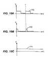
- FIGS. 10A , 10 B, 10 Care representative graphs of the input voltage to the bias source of FIG. 9 .
- FIG. 11is a diagram of portions of the control modules for a row of pixels
- FIG. 12is a circuit diagram of an oscillator.
- FIG. 13is a schematic diagram of a circuit module of FIG. 2 , a corresponding dipole antenna of FIG. 3 , and a graphical representation of the output of a binary counter.
- FIG. 14is a circuit diagram of the pulse counter of FIG. 13 .
- FIGS. 15 , 16 , 17 , 18 , and 19are top views of alternative dipole arrangements.
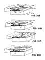
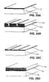
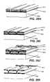
- FIGS. 20A through 20Dare perspective views of a cavity device.
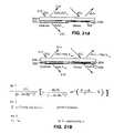
- FIGS. 21A and 21Bare side views of the cavity device.
- FIGS. 22A through 22Fare graphs of frequency responses of the cavity device in different states.
- FIGS. 23A and 23Bare top and cutaway side views, respectively, of a display.
- FIGS. 23C and 23Dare top and cutaway side views, respectively, of another display.
- FIG. 24Ais a graph of an electromechanical response of the cavity device.
- FIG. 24Bis a graph of an addressing and modulation scheme for a display.
- FIGS. 25A through 25N and FIGS. 26A through 26Kare perspective views of the device during assembly.
- FIGS. 27A through 27Care side views of dielectric mirrors.
- FIG. 27Dis a top view of a dielectric mirror.
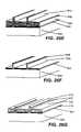
- FIGS. 28A , 28 Bare perspective and top views of a linear tunable filter.
- FIGS. 29A , 29 Bare perspective and top views of a deformable-mirror.
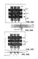
- device 20includes a screen 22 for displaying or sensing a high resolution color image (or a succession of color images) under control of power and control circuitry 26 .
- the imageis made up of a densely packed rectangular array of tiny individual picture elements (pixels) each having a specific hue and brightness corresponding to the part of the image represented by the pixel.
- the pixel density of the imagedepends on the fabrication process used but could be on the order of 100,000 pixels per square centimeter.
- each pixelis generated by one so-called tri-dipole 30 .
- the boundary of each tri-dipoleis T-shaped.
- the tri-dipolesare arranged in rows 32 in an interlocking fashion with the “Ts” of alternating tri-dipoles oriented in one direction and the “Ts” of intervening tri-dipoles along the same row oriented in the opposite direction.
- the rowstogether form a two-dimensional rectangular array of tri-dipoles (corresponding to the array of pixels) that are arranged on a first, external layer 34 of screen 22 .
- the arraymay be called an electrically alterable optical planar array, or a visible spectrum modulator array.
- tri-busses 38are arranged in an interlocking two-dimensional array 40 corresponding to the layout of the tri-dipoles on layer 34 above.
- Each tri-dipole 30is connected to its corresponding tri-bus 38 by a multi-conductor link 42 running from layer 34 to layer 36 in a manner described below.
- a set of circuit modules 46are arranged in a two-dimensional rectangular array corresponding to the layouts of the tri-dipoles and tri-busses.
- Each circuit module 46is connected to its corresponding tri-bus 38 by a six-conductor link 48 running from layer 36 to layer 44 in a manner described below.
- Each circuit module 46electronically controls the optical characteristics of all of the antennas of its corresponding tri-dipole 30 to generate the corresponding pixel of the image on screen 22 .
- Circuit modules 46are connected, via conductors 50 running along layer 44 , to an edge of layer 44 .
- Wires 52connect the conductors 50 to control and power circuitry 26 which coordinates all of the circuit modules 46 to 25 generate the entire image.
- each tri-dipole 30has three dipole sections 60 , 62 , 64 .
- the center points 59 , 61 , 63 of the three sectionsare arranged at 120 degree intervals about a point 65 at the center of tri-dipole 30 .
- Each section 60 , 62 , 64consists of a column of dipole antennas 66 , 68 , 70 , respectively, only ten dipole antennas are shown in each section in FIG.
- each dipole antennaOnly the two arms of each dipole antenna are exposed on layer 34 , as shown in FIG. 3 .
- the dipole antennas of a given sectionall have the same dimensions corresponding to a particular resonant wavelength (color) assigned to that section.
- the resonant wavelengths for the three sections 60 , 62 , 64are respectively 0.45 microns (blue), 0.53 microns (green), and 0.6 microns (red).
- each dipole antenna 80schematically includes two Ls 82 , 84 respectively made up of bases 86 , 88 , and arms 90 , 92 .
- the bases of each antenna 80are electrically connected to the corresponding circuit module 46 .
- the span (X) of arms 90 , 92is determined by the desired resonant wavelength of dipole antenna 80 ; for example, for a resonant wavelength of lambda, X would be lambda/2.
- Dipole antennas 66 , 68 , 70have X dimensions of 0.225 microns (lambda 1 ,/2), 0.265 microns (lambda 2 /2), and 0.3 microns (lambda 3 ,/2), respectively.
- the effective length (Y) of bases 86 , 88 from arms 90 , 92 to circuit module 46is also a function of the dipole antenna's resonant wavelength; for a resonant wavelength of lambda, Y is a multiple of lambda.
- each of the bases 86 , 88physically is made up of four segments; (1) one of the conductors 96 of link 42 , (2) a portion 112 of tri-bus 38 , (3) a short connecting portion 124 of tri-bus 38 , and (4) one of the conductors 94 of link 48 , which together define a path (e.g., the path shown as dashed line 97 ) with an effective length of Y from the arm (e.g., 92 ) to the circuit module 46 .
- a pathe.g., the path shown as dashed line 97
- Spacing Zmay be chosen based on the bandwidth/gain tradeoff, and for example may be one quarter of the resonant wavelength for the dipole antennas of a given section (i.e., lambda/4, or 0.1125 microns (lambda 1 /4), 0.1325 microns (lambda 2 /4) and 0.15 microns (lambda 3 /4) for antennas 66 , 68 , 70 , respectively).
- each tri-bus 38is formed of aluminum on layer 36 and has three zigzag shaped bus pairs 100 , 102 , 104 for respectively connecting dipole antennas of the corresponding sections 60 , 62 , 64 of tri-dipole 30 .
- Bus pairs 100 , 102 , 104are connected to individual dipole antennas 66 , 68 , 70 via conductors of link 42 ( FIG. 2 ) that are joined to the bus pairs at points, e.g., 106 .
- Each bus pair 100 , 102 , 104has two parallel buses 108 , 110 .
- Bus 108electrically connects together the arms of the dipole antenna 5 of the corresponding section and, independently, the related bus 110 electrically connects together the arms 92 of the dipole antennas of that same section.
- Points 106delineate a series of fragments 112 , 114 , 116 on each of the three bus pairs 100 , 102 , 104 , respectively. Each fragment forms part of one or more of the bases 86 , or 88 and therefore contributes to the effective Y dimension.
- the lengths (Q) of fragments 112 , 114 , 116are one-half of the resonant wavelengths (i.e. lambda/2) of the sections 60 , 62 , 64 , or 0.225 microns (lambda 1 ,/2), 0.265 microns (lambda 2 ,/2), and 0.3 microns (lambda 3 ,/2), respectively.
- the conductors of link 48( FIG. 2 ) are attached to tri-bus 38 at points 118 , 120 , 122 at the ends of buses 108 , 110 .
- fragments 124 , 126 , 128are included between points 118 , 120 , 122 and the first points 106 on along buses 108 , 110 .
- the lengths of the three fragments 124 , 126 , 128are 0.1125 microns, 0.1525 microns, and 0.1875 microns, respectively.
- each dipole antenna 80is physically formed (of aluminum) on an insulating semiconductor (e.g. silicon dioxide of silicon nitride) substrate 130 (part of layer 34 ) by x-ray or electron beam lithography or other technique suitable for forming submicron-sized structures.
- an insulating semiconductore.g. silicon dioxide of silicon nitride
- Tri-busses 38are formed on the upper-side of a second insulating semiconductor substrate 132 (part of layer 36 ).
- Circuit modules 46(not seen in FIG. 7 ) are part of a third insulating semiconductor substrate 134 (part of layer 44 ) and are connected by conductors 50 to gold contact pads 136 (only one shown, not to scale) formed on the edge of substrate layer 134 .
- circuit module 46is formed in and on substrate 134 by any one of several monolithic processes.
- a section 138 of the substrate 134which has been previously coated with an insulating semiconductor oxide layer 140 , is repeatedly masked (whereby small windows are opened in the oxide layer, exposing the semiconductor beneath) and exposed to n and p dopants to form the desired circuit elements (not shown in detail in FIG. 8 ).
- the individual circuit elementsare connected to each other and to external contact pad 136 ( FIG. 7 ) by aluminum conductors 142 , 50 , respectively.
- aluminum conductors 142 , 50are connected to each other and to external contact pad 136 ( FIG. 7 ) by aluminum conductors 142 , 50 , respectively.
- holes 144are opened in oxide layer 140 and a sheet of aluminum is deposited, filling holes 144 .
- the unwanted aluminumis removed, leaving only conductors 142 , 50 .
- Semiconductor substrate layer 13 . 2is deposited directly on top of the remaining exposed oxide layer 140 and conductors 142 , 50 .
- Holes 146(one shown) (opened using a suitable lithographic technique) are channels for the electrical conductors 147 of links 48 , which connect tri-bus 38 and circuit module 46 .
- Tri-bus 38is etched from a sheet of aluminum deposited onto the surface of layer 132 . The deposition process fills holes 146 , thereby forming the conductors of links 48 .
- Substrate layer 130is deposited onto the surface of substrate layer 132 and tri-bus 38 .
- the arms of dipole antennas 80are formed by depositing a sheet of aluminum onto the surface of layer 130 and etching away the unwanted metal. During the deposition process holes 148 are filled thereby forming the conductors 149 of links 42 between the arms of dipole antenna 80 and tri-bus 38 .
- the conductors 149are the uppermost parts of bases 86 , 88 ( FIG. 4 ) of dipole antennas 66 , 68 , 70 ; the lengths of conductors 149 together with the lengths of fragments 112 , 114 , 116 ( FIG. 6 ), the lengths of fragments 124 , 126 , 128 , and the lengths of the conductors 147 determine the effective Y dimension of bases 86 , 88 .
- the length of the conductors 149is determined by the thickness of the substrate 130 through which links 42 pass.
- Substrate 130 and links 42are 0.05625 microns (i.e. lambda 1 ,/8) thick. This thickness is achieved by controlling the deposition rate of the semiconductor material as layer 130 is formed.
- the length of the conductors 149is determined by the thickness of the substrate layer 132 through which they pass. This, layer and links 48 are therefore also 0.05625 microns 20 thick.
- the Y dimensions for the dipole antennas 66 , 68 , 70 of sections 60 , 62 , 64therefore are as follows:
- Yequals the sum of 0,05625 microns (length of conductor in link 42 , lambda 1 /8)+n*0.3 microns (where 0.3 microns ⁇ lambda 3 /2, the length of a fragment 116 , and n equals the number of fragments 116 in each base 86 , 88 of the nth dipole antenna 70 n )+0.1875 microns (the length of fragment 128 , (lambda 3 /2) ⁇ (lambda 1 /4))+0.05625 microns (length of conductor in link 48 ), and that sum equals (n+1)*(lambda 3 /2).
- the displayed imageis not emitted from device 20 but is comprised of ambient light (or light from a source, not 25 shown) selectively reflected by the tri-dipoles 30 of screen 22 .
- each tri-dipole 30receives ambient light having a broad spectrum of wavelengths and is controlled by the corresponding circuit module to reflect only that portion of the ambient light manifesting the hue and brightness of the desired corresponding pixel.
- the hue generated by tri-dipole 30depends on the relative intensities of the light reflected by sections 60 , 62 , 64 .
- the overall brightness of that hue of lightin turn depends on the absolute intensities of the light radiation reflected by sections 60 , 62 , 64 .
- both the hue and brightness of the light generated by tri-dipole 30can be controlled by regulating the intensity of the light reflected by the dipole antennas in each section of the tri-dipole; this is done by controlling the reflectivity of each dipole antenna, i.e. the percentage of the light of the relevant wavelength for that dipole antenna which is reflected.
- the desired percentageis attained not by regulating the amount of light reflected at any given instant but by arranging for the antenna to be fully reflective in each of a series of spaced apart time slots, and otherwise non-reflective.
- Each dipole antennain conjunction with its circuit module, has only two possible states: either it reflects all of the light (at the antenna's resonant frequency), or it reflects none of that light.
- the intensityis regulated by controlling the percentage of total time occupied by the time slots in which the dipole antenna occupies the first state.
- Each dipole antennais controlled to be reflective or not by controlling the impedance of the dipole antenna relative to the impedance of the medium (e.g., air) through which the light travels.
- the mediume.g., air
- E _ _x ⁇ ⁇ E _ t ⁇ e - j ⁇ ⁇ k c ⁇ z ( 3 )
- H _ _y ⁇ ⁇ 1 ⁇ t ⁇ E _ t ⁇ e - j ⁇ ⁇ k t ⁇ z ( 4 )
- ⁇ _E _ R
- T _ - 1⁇ N - 1 ⁇ n + 1 ( 10 )
- the impedance Z L , of dipole antenna 80is controlled by a variable resistance PIN diode 160 connected across bases 86 , 88 .
- PIN line 162to the output of a bias high voltage or a low voltage based on a line 168 from power and the output of bias source 164 is a high voltage
- the resistance R of PIN diode 160 (and hence the impedance (E,) of the dipole antennais zero causing full reflection
- resistance Ris set to a value such that the resulting impedance z@ is matched to z. (the impedance of the air surrounding the antenna), causing zero reflection.
- power and control circuitry 26receives a video signal (e.g. a digitized standard RGB television signal) and uses conventional techniques to deliver corresponding signals to modules 46 which indicate the relative desired intensities of light reflected from all sections 60 , 62 , 64 of all of the tri-dipoles in the array at a given time.
- Circuit modules 46use conventional techniques to deliver an appropriate stream of input control signal pulses to each bias source 164 on line 168 .
- pulse stream 170has a period T and a 50% duty cycle.
- the input to bias source 164is high and the Corresponding output of source 164 is a high voltage.
- dipole antenna 80will reflect all received light having the dipole antenna's resonant wavelength.
- the output of source 164will be low and dipole antennas 80 will absorb the received light.
- pulse streams 172 , 174represent a 30% duty cycle and a 100% duty cycle respectively; with a 30% duty cycle the effective intensity of the light radiation of the dipole antennas of the section will be 30%; for a duty cycle of 100%, the effective intensity is 100%.
- the relative intensities required of the three red, 25 green, and blue sections 60 , 62 , 64may be, respectively, 30 , 40 , and 10 .
- the input signals to the bias sources 164 , carried on lines 168would then have duty cycles, respectively, of 30%, 40%, and 10%.
- An adjacent pixel which is to be a brown of the same hue but greater brightnessmight require duty cycles of 45%, 60%, and 15%.
- each circuit module 46 in the rowincludes storage 180 , 182 for two bits.
- the bit 1 storage elements 180 of the modules 46 in the roware connected together to create one long shift register with the pulse width modulated signals being passed along the row data line 184 from pixel to pixel. If, for example, the period of the modulated signals is 1 millisecond and there are ten different intensity levels, then an entire string of bits (representing the on or off state of the respective pixels in the row during the succeeding 1/10 millisecond) is shifted down the row every 1/10 millisecond.
- each element 182is the input to the driver 188 for the appropriate one of the three colors of that pixel, which in turn drives the corresponding section 60 , 62 , 64 of the tri-dipole.
- the rate at which data is shifted along the shift registersis determined by the number of elements on a given row, the number of rows, the number of intensity levels, and the refresh rate of the entire array.
- the light comprising the imageis emitted by tri-dipoles 30 rather than being produced by reflected ambient light.
- each tri-dipolegenerates the light for a single pixel with a hue and brightness governed by the intensities of the light emitted by each of the three sections 60 , 62 , 64 .
- Each dipole antenna within a tri-dipoleis caused to emit light at the resonant wavelength of that antenna by stimulating it using a signal whose frequency corresponds to the resonant wavelength.
- the sections 60 , 62 , 64will emit blue (lambda 1 ), green (lambda 2 ), and red (lambda 3 ) light respectively when provided with signals whose frequencies equal, respectively, lambda 1 , lambda 2 and lambda 3 .
- ⁇represents the angle relative to the dipole
- ⁇ (hat)is the angular orientation of the wave
- ⁇ 0the permeability of free space
- ris radius from the dipole
- r(hat)is radial orientation of the wave
- a ris the radial component of the vector potential
- a ⁇is the angular component of the vector potential
- kis a factor which is used to represent sinusoidally varying waves.
- the H fieldis given by
- Equation (16)describes the radiation pattern away from a dipole antenna at distances significantly greater than the wavelength of the emitted electromagnetic wave. It is a very broad radiation pattern providing a wide field of view at relevant distances.
- the dipole antennas 66 , 68 , 70 of each section 60 , 62 , 64are driven by signals (e.g., sinusoidal) with frequencies of 5 ⁇ 10 14 Hz, 5.6 ⁇ 10 14 Hz, and 6.6 ⁇ 10 14 Hz for red, green, and blue, respectively.
- signalse.g., sinusoidal
- These signalsare supplied by three monolithic oscillators 200 (one shown) within circuit module 46 , each tuned to one of the three required frequencies.
- circuit 200an a stable multivibrator
- the center pair of coupled transistors 202 , 204are the primary active elements and will oscillate if the circuit admittance's are set appropriately.
- Diodes 206 , 208 , 210 , 212provide coupling capacitance's between the transistors and the inductors 214 , 216 are used to tune the operating frequency.
- an image of the objectis focused by a conventional lens (not shown in FIG. 1 ) onto screen 22 , which then acts as an image sensor.
- the tri-dipoles of screen 22controlled by power and control circuitry 26 , generate electrical signals corresponding to pixels of the received image.
- the signalsare then processed by a processor which, in conventional fashion, delivers a derived RGB video signal which can then be transmitted or stored.
- the signals generated for each tri-dipoleare generated by the corresponding circuit module 46 and represent the hue and brightness of the light radiation received at that tri-dipole.
- circuit module 46can, by independently measuring the intensity of the light radiation received at each section 60 , 62 , 64 , derive a signal which specifies the hue and intensity of the received pixel.
- dipole antenna 80will absorb incident light radiation at its resonant wavelength when its reflection coefficient ( ⁇ L ) is zero, which occurs when its controlled impedance (z L ) matches the impedance of the medium (z 0 ). In those circumstances, a voltage pulse is produced across the ends 308 , 310 of dipole 80 for each incident photon. The relative magnitude of the light radiation received by each dipole antenna can thus be measured by counting the average number of pulses across ends 308 , 310 over a given time period.
- circuit module 46includes a terminating load resistor 315 connected across ends 308 , 310 .
- the controlled impedance of the combination of dipole antenna 80 and resistor 315is equal to z 0 .
- a pulse detector 318amplifies and sharpens the resulting pulse to a square wave form as shown, which is then used as the clock (CLK) input 319 to a binary counter 320 .
- the output of the binary counteris sampled at a regular rate; collectively the samples form a digital signal representing the intensity of received light radiation over time.
- Each time counter 320is sampled, it is reset to zero by a pulse on control line 322 ,
- Counter 320thus serves as a digital integrator that indicates how much light arrived in each one of a succession of equal length time periods.
- the pair of transistors 322 , 324serve as a high impedance differential stage whose output (representing the voltage difference between points 308 , 310 ) is delivered to an amplifier 326 .
- Amplifier 326serves as a high-bandwidth gain stage and delivers a single sided output pulse to a conditioning circuit 328 that converts slow rising pulses to square pulses 330 for driving counter 320 .
- the array of tri-dipolesis operated as a phased array.
- phased arraysThe operation of phased arrays is discussed more fully in Amitay, et al., Theory and Analysis of Phased Array Antennas, 1972, incorporated herein by reference.
- wave cancellation or reinforcementcan be used to control the direction in three dimensions and orientation of the radiation. Beams can thus be generated or scanned.
- the arraycan be made more sensitive to radiation received from selected directions.
- each section of tri-dipole 400 arraybe a single dipole antenna 406 , 407 , 408 .
- the tri-dipole antennasare then arranged about a center Point 410 at 120 degree intervals in a radial pattern.
- Bases 411 , 412 , as well as arms 414 , 415 , of the dipole antennas,are all formed on the same surface.
- each sectionmay consist of multiple dipole antennas 406 , 407 , 408 connected by attaching the bases 411 , 412 of each succeeding dipole antenna to the inner ends of arms 414 , 415 of the preceding dipole antenna.
- Circuit modules 416are formed on the surface of layer 413 .
- a multi-dipole 430could have five sections 432 , 434 , 436 , 438 , 440 composed of dipole antennas 442 , 444 , 446 , 448 , 450 , respectively.
- the dipole antennas of the different sectionswould have different resonant wavelengths.
- Other multi-dipolesmight have any number of sections.
- the scanning of pixelscould be done other than by pulse width modulation, for example, using charge coupled devices to shift packets of charge along the rows of pixels.
- FIGS. 18 , 19other arrangements of dipole antennas may be used in order to match the area required for the control circuit modules.
- each section 470 of a tri-dipole in the reflective modecould be formed of a number of subsections (e.g., 472 ) arranged in two rows 474 and a number of columns 47 .
- the antennas 478 in each subsection 472are all served by a single PIN diode circuit 480 located at the peripheral edge of section 470 at the end of the subsection on the layer below the antenna layer. All circuits 480 for the entire Section 470 are in turn served by a single bias source 164 ( FIG. 9 ). This arrangement reduces the number of bias sources required for the entire array of tri-dipoles.
- FIG. 19shows an alternate arrangement in which there is but one row of subsections each served by a single PIN diode circuit at the end of the row.
- selected tri-dipolescould be used to receive control signals transmitted directly by light and to pass those control signals to the control circuits of nearby active tri-dipoles.
- the dipolescould be mono-dipoles comprised of only a single dipole antenna, all with the same resonant wavelength.
- Dipole antennas 470could be randomly arranged on the surface of layer 472 of screen 22 .
- RGBRed, Green, Blue
- the arraycould be three-dimensional.
- the successive tri-dipoles in the arraycan be oriented so that their respective antennas are orthogonal to each other to enable the array to interact with radiation of any arbitrary polarization.
- the PIN diodescould be replaced by other impedance controlling elements. Such elements might include quantum well transistors, superconducting junctions, or transistors based on vacuum microelectronics. Further improvement could be achieved by reducing the complexity of the third layer containing control circuitry. The electronics required to get control signals to the circuitry could be eliminated by the use of laser or electron beams to provide such signals. This would have the advantage of allowing for arrays of even higher density.
- the arraycould be fabricated on a transparent substrate, thus facilitating transmissive operation.
- the antenna arraysalone (without control circuitry or connection buses) may be fabricated on one-half of a microfabricated interferometric cavity.
- the antenna arraycan be considered a frequency selective mirror whose spectral characteristics are controlled by the dimensions of the antennas.
- Such a cavitywill transmit and reflect certain portions of incident electromagnetic radiation depending on (a) the dimensions of the cavity itself and (b) the frequency response of the mirrors.
- the behavior of interferometric cavities and dielectric mirrorsis discussed more fully in Macleod, H. A., Thin Film Optical Filters, 1969, incorporated by reference.
- two example adjacent elements of a larger array of this kindinclude two cavities 498 , 499 fabricated on a transparent substrate 500 .
- a layer 502the primary mirror/conductor, is comprised of a transparent conductive coating upon which a dielectric or metallic mirror has been fabricated.
- Insulating supports 504hold up a second transparent conducting membrane 506 .
- Each array elementhas an antenna array 508 formed on the membrane 506 .
- the two structures, 506 and 508together comprise the secondary mirror/conductor.
- the antenna arraymay be fabricated as part of the primary mirror/conductor.
- Secondary mirror/conductor 506 / 508forms a flexible membrane, fabricated such that it is under tensile stress and thus parallel to the substrate, in the undriven state.
- the interferencewill determine its effective impedance, and thus its reflective and/or transmissive characteristics.
- the cavity heighti.e., the spacing between the inner walls of layers 502 , 506
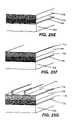
- the change in heightis achieved by applying a voltage across the two layers at the cavity, which, due to electrostatic forces, causes layer 506 to collapse.
- Cavity 498is shown collapsed (7 volts applied), while cavity 499 is shown uncollapsed (o volts applied).
- each cavitymay be formed by a combination of dielectric or metallic mirrors on the two layers, and without the antennas formed on either layer.
- the spectral characteristics of the mirrorare determined by the nature and thickness(es) of the materials comprising it.
- each cavityis fabricated using a simpler process which precludes the need for separately defined support pillars.
- each secondary mirror/conductor, 506is formed in a U-shape with the legs attached to the primary layer; each secondary mirror/conductor thus is self-supporting.
- FIG. 20 dthe cavity has been modified to alter it's mechanical behavior.
- a stiffening layer, 510has been added to limit deformation of the membrane while in the driven state. This assures that the two mirrors will remain parallel as a driving voltage is gradually increased.
- the resulting devicecan be driven in analog mode (e.g., cavity 511 may be driven by 5 volts to achieve partial deformation of the cavity) so that continuous variation of its spectral characteristics may be achieved.
- the binary modulation modeis shown in FIG. 21A .
- incident light 512(the delta lambda represents a range of incident frequencies, e.g., the range of visible light) contains a spectral component which is at the resonant frequency of the device in the undriven state. Consequently this component (delta lamba n) is transmitted, 516 , and the remaining components (at nonresonant frequencies, delta lambda minus delta lamba n) are reflected, 514 .
- This operationis in the nature of the operation of a fabry-perot interference cavity.
- the resonant frequency of the deviceWhen the device is driven and the geometry altered to collapse (right side of figure), the resonant frequency of the device also changes. With the correct cavity dimensions, all of the incident light (delta lamba) is reflected.
- FIG. 21Ashows a binary mode of operation while FIG. 21B shows an analog mode, where a continuously variable voltage may be used to cause a continuously variable degree of translation of secondary mirror/conductor 506 .
- Thisprovides a mechanism for continuous frequency selection within an operational range because the resonant frequency of the cavity can be varied continuously.
- the transmitted wavelengthsare delta lambda n zero, while in the right hand side they are delta lambda n one.
- Equation 1defines the transmission T through a fabry-perot cavity.
- Ta, Tb, Ra, Rbare the transmittances and reflectances of the primary (a) and secondary (b) mirrors.
- Phi a and Phi bare the phase changes upon reflectance at the primary and secondary mirrors, respectively.
- Deltais the phase thickness.
- Equation 2defines the phase thickness in terms of the cavity spacing ds, the index of refraction of the spacer ns, and the angle of incidence, theta s.
- Equation 3shows that the transmission T becomes the transmission of the second mirror when the transmission of the first mirror approaches 0.
- FIGS. 22A through 22Fillustrate some of the possibilities and relate to the equations of FIG. 21B . These are idealized plots which illustrate transmission and reflectivity (T/R) of the cavity for wavelengths in the visible range in driven and undriven states for each of the driven and undriven response modes. The different modes are achieved by using different combinations of mirrors and cavity spacings.
- the spectral characteristics of the mirrors usedcan be referred to as broad-band and narrow-band.
- the mirrorsare optimized for the visible range with a broad band mirror operating across the entire visible range (i.e., reflecting over a minimum range of 400 nm to 700 nm).
- a broad band mirroroperating across the entire visible range (i.e., reflecting over a minimum range of 400 nm to 700 nm).
- Such a mirroris denoted in the stack formula 1.671 ⁇ 0.775(ERS) 0.833M (ERS) ⁇ 1.671 where ERS denotes an equal ripple filter.
- a narrow-band filter optimized for the color greenwould reflect only over the range of 500 nm to 570 nm, and transmit everywhere else.
- the cavity spacing(i.e., cavity height) in both driven and undriven states can be set to a predetermined value by the film thicknesses used in its construction. These two values determine whether a cavity is resonant or non-resonant. For a resonant cavity, the spacing is determined such that the undriven state coincides with the resonant peak of the narrower of the two mirrors. When a device is non-resonant, it must be driven in order for the device to become resonant.
- FIG. 22Ashows a T/R plot of a cavity having broad band mirrors on both layers of the cavity.
- thisresults in transmission/reflection peaks which occur at wavelengths which are approximately integral multiples of the cavity spacing.
- the notation m delta lambda n in FIG. 21Adenotes the fact that there may be a series of peaks.
- Thisis classic fabry-perot behavior.
- the driven stateshown to the right in FIG. 22A
- the cavity resonanceis shifted out of the visible range causing the device to act like a broadband mirror.
- FIG. 22Bshows a T/R plot for a cavity having one broad band and one narrow band mirror.
- This devicehas a resonant cavity, causing a transmission peak at the center of the narrow-band mirror's passband when the device is in the undriven state.
- Driving the device(right hand side of FIG. 22B ) shifts the cavity resonance away from that of the narrow band mirror, and the device acts like a broadband mirror.
- the cavityis like that of FIG. 22B , except the cavity is non-resonant which results in broadband mirror cavity behavior in the undriven state.
- the cavity spacingshifts into resonance, causing a transmission peak centered on the narrow-band mirror.
- FIG. 22Dshows the performance of a resonant cavity with two narrow-band mirrors.
- the overall cavity responseis that of a broad-band transmitter.
- Driving the device out of resonancei.e. active
- the cavity of FIG. 22Ehas two narrow band mirrors, but it is a non-resonant cavity. Consequently its behavior is opposite that of the cavity portrayed in FIG. 22D .
- the transmissionapproaches zero for frequencies outside its range. This is essentially the transmission of mirror b.
- the transmissionbecomes a maximum outside the frequency range. In either case, the spurious peaks typical of a fabry-perot are avoided. The result is a device which can be described as a single mode resonant cavity.
- both of the mirrorsare narrow banded, then fabry-perot type behavior occurs only when the cavity spacing is correct. Making the mirrors narrow enough allows only a single peak to occur. Then it is unnecessary to be concerned about spurious peaks that might occur within the visible range.
- FIG. 22Fis for a cavity with a simpler design involving only a metallic mirror on one wall and a hybrid filter on the other wall.
- the hybrid filteris a combination of a narrow bandpass filter (outer surface) and an induced absorber (inner surface).
- the induced absorberis a simple structure which can consist of one or more dielectric or dielectric and metallic films. The function of the absorber is to cause incident light of a specified frequency range to be absorbed by a reflective surface (i.e. mirror).
- the induced absorberonly functions when it is in contact with the mirror, otherwise it is inconsequential.
- the hybrid filter(a green centered narrow bandpass/induced absorber) reflects everything but the green light, which is unaffected by the induced absorber and subsequently reflected by the metallic mirror.
- the overall cavity responseis like that of a broad-band mirror.
- the hybrid filtercomes into contact with the metallic mirror.
- the absorbercouples the green light into the mirror, and the result is an absorption peak at that wavelength.
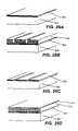
- a red 3 ⁇ 3 pixel (i.e., 9 cavities) subtractive mode display array based on the cavity device using the N—N (narrow band-narrow band) configuration of FIG. 22Dis shown.
- the cavity pixelsare formed at the intersections of primary mirror/conductors 602 and secondary mirror/conductors 604 .
- the displayis fabricated on substrate 608 and driven via contact pads 606 connected to each conductor/mirror 604 .
- a full nine-pixel displaycomprises three replications of the array of FIG. 23A arranged on top of one another and fabricated on separate substrates or color planes 610 , 612 , 614 , as shown in FIG. 23B .
- Each of the individual color planesinteracts only with and reflects one color (e.g., red, green, or blue), while passing all other colors. This is done by selecting the mirror spectral characteristic and cavity spacing in each color plane appropriately.
- the color planesare physically aligned and electrically driven through the contact pads to produce full color images. The image would be viewed from below in FIG. 23B .
- FIGS. 23C and 23Da single layer composite approach is shown. Such a device would be more complicated to fabricate (though the mirror designs are simpler) but may suffer from inferior resolution. In this case, all three colors reside on the same array 616 .
- Either the three plane or the single plane approachmay be used in either transmissive and reflective modes.
- Pixel size and overall display sizecan be altered to make LO the displays useful in many different display and spatial light modulator applications. These include direct view and projection displays, optical computing, holographic memory, and any other situation where a one or two dimensional modulator of light can be used.
- the secondary mirror/conductorexperiences a displacement towards the substrate until the force of restoration balances the electrical attraction.
- the force of restorationis completely overcome and the membrane is pressed tightly against the substrate.
- the voltagecan then be lowered again to some degree without affecting the position of the membrane. Only if the voltage is then lowered significantly or eliminated will the membrane be released. Because the membrane is under tensile stress, it will then pull itself away from the substrate when the voltage is released. This hysteresis can be used to achieve matrix addressing of a two-dimensional array, as explained with reference to FIG. 24B .
- the displaycan be addressed and brightness controlled using control pulse sequences in the driving voltage. Shown is a timing diagram for a 3 ⁇ 3 pixel array analogous to that shown in FIG. 23A .
- a continuous series of ⁇ 5 volts scanning pulsesis applied to the rows (rows 1–3) of the pixel array in a sequential fashion, as seen in the charts labelled “Row”.
- the pulsesappear at the same frequency on each of the rows but the pulses for different rows are staggered. These pulses are insufficient in their own right to cause the membrane to collapse.
- the columns (cols. 1–3) of the pixel arrayare maintained at a bias voltage of 5 volts so that the nominal voltage across each unactivated pixel is 5 volts.
- the nominal row and column potentialsare 5 and ⁇ 5 volts respectively, resulting in a cavity voltage of 10 volts.
- the total voltage across the cavitybecomes 15 volts which is sufficient to drive the secondary mirror/conductor into the collapsed state, where it will remain until the end of the scan when all of the column voltages are pulsed to zero.
- the three charts at the bottom of FIG. 24Bshow the on and off states of the three pixels identified there by row and column numbers.
- the intensity or brightness of a pixelmay be varied by changing the fraction of the scan during which the pixel is activated.
- the scan cyclebegins at 198 and ends at 199 .
- the frequency of the scan pulsesis such that six pulses of a given row fall within the scan cycle, providing an opportunity to activate a pixel at any one of six times during each cycle. Once the pixel is activated it stays on until the end of the cycle. Therefore six different intensities are possible for each pixel. For the scan shown, pixel C1R1 is at full brightness, pixel C2R2 is at 4/6 brightness, and pixel C3R2 is at 1 ⁇ 6 brightness. All pixels are cleared at the end of the scan and the cycle begins again. Since these structures can be driven at frequencies as high as 50 kHz, this method of brightness control is practical. Assuming six brightness levels, there would be a possibility of more than 8 thousand row scans per second.
- substrate 700is first cleaned using standard procedures.
- the substratemay be of many different materials including silicon, plastic, mylar, or quartz.
- the primary requirementis that the material be able to support an optically smooth, though not necessarily flat, finish.
- a preferred materialwould likely be glass, which would permit both transmissive and reflective operation in the visible range.
- the substrateis then coated with the primary conductor/mirror layer(s) 702 .
- Thiscan be achieved using a physical vapor deposition (PVD) method such as sputtering or e-beam evaporation.
- PVDphysical vapor deposition
- Other possible methodsinclude chemical vapor deposition and molecular beam epitaxy.
- the dimensions and nature of the layer(s)depend on the specific configuration desired. Detailed examples are discussed below.
- a photoresist 704has been patterned on the primary conductor/mirror.
- the photoresistmay be of a positive or negative type.
- the standard procedure for this stepinvolves spinning of the resist, softbaking at 90° C., exposing through an appropriate mask, developing to produce the pattern, and hardbaking at 130° C.
- the photoresist patternis defined in the primary conductor/mirror by an etching process.
- This stepcan be achieved either by wet chemical means or by plasma or reactive ion etching (RIE).
- RIEreactive ion etching
- the choice of etching techniquedepends on the nature of the conductor/mirror. In the case of an aluminum conductor/mirror, chlorine gas may be used to perform the etch, with a standard chamber power of 100 watts producing an etch rate of 100 angstroms/min. Some mirror materials may resist RIE and in such cases a technique such as ion milling may be used. All RIE steps are performed at a pressure of 30 mtorr unless otherwise noted. All plasma etch steps are performed at a pressure of 100 mtorr unless otherwise noted. The photoresist is removed using standard solvents.
- the conductor/mirrormay be defined using the well-known procedure called lift-off. This procedure is used to define a layer in a subsequent step and is described below.
- support rail material 706has been deposited using one of the methods mentioned previously.
- This materialshould be an insulator, for example silicon dioxide or silicon nitride.
- the materialshould be deposited uniformly, and at a thickness equal to thickness of the spacer layer, which will be deposited later. This thickness should in general be at least a multiple of the wavelength of light of interest. A thickness of 0.5 microns would place such a device near the middle of the visible spectrum.
- photoresist layer 708is spun on and hardbaked. Since this layer will not be photolithographically defined, other polymeric materials may be used instead. The only requirement is that they dissolve in solvents such as acetone or methanol, and be able to withstand a vacuum. This is the first step in defining a lift-off stencil.
- template layer 710has been deposited using one of the methods of PVD.
- the layeris of silicon dioxide though other materials are possible. Ideally the material should be etched using a process which does not affect the underlying resist.
- Buffered Oxide Etch (BOE)which consists of Hydrofluoric acid diluted 7:1 with water can perform this step in 15 seconds.
- the layerneed only be a thousand angstroms thick.
- photoresist layer 712has been spun-on and patterned in a manner already discussed.
- the pattern of resist layer 711has been transferred to layers 710 and 708 .
- the BOEis used to etch through the silicon dioxide layer 710 .
- An oxygen plasmais used to etch through resist layer 708 , and to remove resist layer 711 .
- Plasma etchingdiffers from RIE in that it tends to be less anisotropic, yielding profiles that are not purely vertical.
- resist layer 708has been slightly underetched in order to facilitate removal of the lift-off stencil.
- RIEusing a carbon tetrafluoride chemistry (CF4/02 6:4) is then applied to etching through layer 706 .
- spacer layer 712is deposited using PVD techniques.
- This materialcan be any number of different compounds which can be deposited using this technique. There are two key requirements for such a material. The first is that the material be soluble in water but not in solvents such as acetone or methanol. Example materials include lithium fluoride, aluminum fluoride, and sodium chloride. The second is that it be deposited with extreme uniformity and thickness control.
- the formerallows resulting structures to be underetched without damage by using water as the final etchant.
- Wateris an extremely benign solvent, and makes possible the incorporation of many different mirror, conductor, and structural materials in the final device.
- the spacermay also be composed of a polymeric material such as hardbaked photoresist or polyimide.
- a technique other than spinningmust be used to deposit the polymer. Two such techniques include extrusion and capillary coating. The consequence of using such a spacer is that all subsequent process steps must be low temperature in nature to prevent outgassing and shrinkage of this layer. In this case, the spacer is ultimately removed using an oxygen plasma.
- the stencilis subsequently removed using an ultrasonic acetone bath and methanol rinse. This also removes or lifts off excess deposited spacer material and is what constitutes the final step of the lift-off process.
- a natural overhangmay be produced via overexposure.
- positive photoresistusing a technique known as image-reversal. This would preclude the need to put down a sacrificial photoresist layer and a subsequent Sio2 layer.
- secondary conductor/mirror layer(s) and support membrane ( 714 )are deposited.
- the nature of the conductor/mirroris dependent on the application.
- the support membranemust have a tensile residual stress. Tensile stress is required for two reasons. First so that the resulting membranes will be flat and therefore parallel to the substrate in the quiescent state. Secondly, such structures have a tendency to stick when the membranes come in contact with the substrate. Sufficient tensile stress is required pull the membrane away when the drive voltage is reduced.
- the membranemust have the appropriate optical characteristics as well. For visible light this would mean transparency in the visible region.
- Silicon nitrideis one candidate for this role for it can be deposited using plasma enhanced chemical vapor deposition (PECVD) with controlled stress.
- PECVDplasma enhanced chemical vapor deposition
- Other candidatesinclude silicon dioxide, magnesium fluoride and calcium fluoride, all of which can be deposited using e-beam evaporation with a resulting tensile stress.
- photoresist layer 716has been spun-on and patterned in a manner discussed above.
- layer(s) 714have been etched according to the pattern of resist layer 716 .
- the final etchis accomplished by placing the device in water for a period of time.
- the wateris agitated, and when the devices are fully etched they are dried.
- One variation on this stepinvolves the use of n-butyl alcohol to displace the water when the etch is finished.
- the devicesare then placed in a chamber at approximately 32 degrees centigrade to cause the alcohol to freeze. After this step the devices are placed into a vacuum chamber where the air is then evacuated. This causes the alcohol to sublime and can reduce membrane sticking during the drying phase.
- FIGS. 26A through 26CAnother alternative process has initial steps of assembly shown in FIGS. 26A through 26C , analogous to those shown in FIGS. 25A through 25C .
- photoresist or polymer layer 806is spun on and a stencil layer, 208 , of silicon dioxide is deposited using PVD. This layer must be thicker than the spacer layer to be deposited.
- resist layer 810has been spun-on and patterned using standard procedures.
- this stepuses BOE and an oxygen plasma etch to define a lift-off stencil.
- the spacer materialis chosen and deposited as described in FIG. 25J .
- the stencilis subsequently removed using an ultrasonic acetone bath and methanol rinse.
- the step shown in FIG. 26Iis analogous to that shown in FIG. 25K .
- photoresist layer 814has been spun-on and patterned.
- layer(s) 812have been etched according to the pattern of resist layer 214 .
- the final etchis accomplished in a manner described above.
- All of the materials used for the mirrorsmust be deposited in such a way that their stress can be controlled. Ideally, they are deposited as “stress balanced” which means that the overall stress of the film or film stack is zero. Since the ultimate goal is that the support membrane conductor/mirror combination have an overall tensile stress, conductor/mirror films with compressive stress may be accommodated by having a high stress support membrane.
- the technique of ion assisted e-beam deposition (IABD)precludes the need for such accommodation. Using this technique, the residual stress of almost any film of interest may be controlled by bombarding the substrate with a stream of neutral ions during the deposition process. This make possible the total mechanical decoupling of the support material from the optical material. As a result, emphasis can be placed on depositing an optically neutral support membrane with ideal mechanical characteristics. In the same manner, a “mechanically neutral” (i.e. stressless) conductor/mirror can be deposited with ideal optical characteristic.
- simplest conductor/mirror configuration for an individual cavityis formed from a layer 900 that is either the substrate for the primary conductor/mirror, or the support membrane if this is the secondary.
- Layer 902is a metallic film with a thickness on the order of several hundred angstroms. The film can be of aluminum, silver, or any number of metals, based on the spectral, and resistive properties as well as the ease with which the metal can be etched.
- Layer 904is an insulator and/or reflection enhancement film. This can be formed by oxidizing the metal, if aluminum is being used, in an oxygen plasma thus forming a thin layer of aluminum oxide. Alternatively, insulating layers or reflection enhancement layers may be deposited in a manner discussed before.
- Metallic mirrorsmust be somewhat transmissive and therefore no more than several hundred angstroms thick. Insulator films can have thicknesses from one hundred to several thousand angstroms. Their thickness is determined by the kind of voltages expected in driving the devices.
- the conductor 906is either a transparent film such as indium tin oxide (ITO), or a very thin metallic layer such as gold. Either can be deposited using suitable film deposition methods. Thicknesses for the ITO should be in the range of several thousand angstroms, and metallic conductors less than 100 angstroms.
- 908is a multilayer dielectric stack comprising the mirror. Such a mirror consists of alternating dielectric films with differing indexes of refraction deposited by a suitable PVD process. By choosing films with appropriate thicknesses and indexes, mirrors with tailorable spectral characteristics can be fabricated as is well known in the art. In general, the thickness of the individual layers is one quarter the wavelength of the light of interest.
- these mirrorsmay be deposited using a technique known as codeposition.
- codepositionIn this case, PVD is used to deposit two materials with different refractive indices simultaneously. Using computer control the refractive index of the resulting film can be varied continuously between those of either film. This deposition technique makes possible mirrors with virtually any spectral characteristic.
- a dielectric mirror 908is deposited directly on substrate 900 .
- Metallic conductor 902 and insulator 904are deposited and patterned such that they form a border around the periphery of the mirror. Using this configuration, it is possible to provide drive voltages to the devices without compromising throughput since the conductor can be placed outside the active area of the device.
- FIG. 27Dshows a planar view of this mirror configuration.
- a linear tunable filteris shown which has been fabricated using the process sequence defined above.
- the major differenceis the nature of the mask used to define the self-supporting membrane, which is comprised of support 1006 and 1008 .
- the substrate, 1000is transparent in the frequency region of interest, and electrodes 1004 are used to drive the device.
- Dielectric mirror 1002are defined separately to produce a configuration like that of FIGS. 27 c , 27 d .
- Three filtersare shown though many more can be fabricated. Each filter 1010 , 1012 , and 1014 is driven independently so that individual frequencies may be separated from an incident light beam.
- FIG. 28 bis a top view of the structure.
- a device known as a deformable mirrorincludes a self-supporting membrane 1102 fabricated on a substrate 1100 .
- a potentialis applied between actuator electrodes 1104 and conducting mirror 1106 , the surface of the mirror can be deformed in a controllable manner.
- Such a devicecan be used as a component in an adaptive optics system, or in any situation where control of an incident wavefront is required.
Landscapes
- Physics & Mathematics (AREA)
- General Physics & Mathematics (AREA)
- Optics & Photonics (AREA)
- Engineering & Computer Science (AREA)
- Nonlinear Science (AREA)
- Theoretical Computer Science (AREA)
- Computer Hardware Design (AREA)
- Chemical & Material Sciences (AREA)
- Spectroscopy & Molecular Physics (AREA)
- Crystallography & Structural Chemistry (AREA)
- Nanotechnology (AREA)
- Life Sciences & Earth Sciences (AREA)
- Biophysics (AREA)
- Microelectronics & Electronic Packaging (AREA)
- Electromagnetism (AREA)
- Mechanical Light Control Or Optical Switches (AREA)
- Control Of Indicators Other Than Cathode Ray Tubes (AREA)
Abstract
Description
{overscore (E)}={circumflex over (X)}E0e−jkz+{circumflex over (X)}Ere+jkz (1)
whereE (overbar) is the complex amplitude of the electric field of the sum of the transmitted wave and the reflected wave;E0is the complex amplitude of the electric field of the transmitted20 wave;Er, is the complex amplitude of the electric field of the reflective wave; x(hat) is the orientation of the electric field of the wave; H is the amplitude of the magnetic field; y(hat) is the orientation of the magnetic field; μo is the permeability of free space; ε0is the permittivity of free space; k=ωsqrt[μ0ε0] is the wavenumber; and η=sqrt[μ0/ε0] is the impedance of free space. For z>0 (i.e., within free space) only the transmitted wave exists and is represented by
E(overbar) is the complex amplitude the transmitted wave at z=0, kt=sqrt[με] is its wavenumber; η=sqrt[μ/ε] is the impedance of the medium, i.e. z>0. Boundary conditions (z=0) for tangential electric fields are imposed on
{circumflex over (X)}[E0+Er]={circumflex over (X)}Et (5)
ŷ(1/η0)(E0−ER)=ŷ(1/ηt)Et (6)
1+Er/E0=Et/E0 (7)
1−ER/E0=(η0/ηt)(Et/E0) (8)
Er/E0is called Γ and is the complex reflection coefficient while Et/η0=T is called the complex transmission coefficient, and ηt/η0=ηnis the normalized wave impedance. Solving for T and Γ yields
For matched impedance values, η0=ηn, the reflection coefficient is zero, and T=1 (i.e., no reflection), and in the case of a load at the boundary, a matched antenna, there is complete absorption.
I=jωq (11)
{overscore (J)}({overscore (r)}1)={circumflex over (z)}Idδ({overscore (r)}1) (12)
whereq is the charge density; z(hat) indicates the direction of the current (along the z-axis); ω is angular frequency; and d is the distance between ideal point charges representing the dipole. The vector potentialA(overbar) in polar coordinates is given by
where θ represents the angle relative to the dipole; θ (hat) is the angular orientation of the wave; μ0is the permeability of free space; r is radius from the dipole; r(hat) is radial orientation of the wave; Aris the radial component of the vector potential; Aθ is the angular component of the vector potential; and k is a factor which is used to represent sinusoidally varying waves. The H field is given by
- where φ is elevation, with respect to the dipole. The E field is given by,
- The far-field equation is given by
V(z)=V+e−jkz+ΓLejkz (17)
Because ZL=Z0, ΓL=0, and equation 17 simplifies to
V(z)=V+e−jkz (18)
Claims (43)
Priority Applications (1)
| Application Number | Priority Date | Filing Date | Title |
|---|---|---|---|
| US11/070,497US7012732B2 (en) | 1994-05-05 | 2005-03-01 | Method and device for modulating light with a time-varying signal |
Applications Claiming Priority (6)
| Application Number | Priority Date | Filing Date | Title |
|---|---|---|---|
| US08/238,750US5835255A (en) | 1986-04-23 | 1994-05-05 | Visible spectrum modulator arrays |
| US55463095A | 1995-11-06 | 1995-11-06 | |
| US76994796A | 1996-12-19 | 1996-12-19 | |
| US09/056,975US6674562B1 (en) | 1994-05-05 | 1998-04-08 | Interferometric modulation of radiation |
| US09/966,843US6867896B2 (en) | 1994-05-05 | 2001-09-28 | Interferometric modulation of radiation |
| US11/070,497US7012732B2 (en) | 1994-05-05 | 2005-03-01 | Method and device for modulating light with a time-varying signal |
Related Parent Applications (1)
| Application Number | Title | Priority Date | Filing Date |
|---|---|---|---|
| US09/966,843ContinuationUS6867896B2 (en) | 1993-03-17 | 2001-09-28 | Interferometric modulation of radiation |
Publications (2)
| Publication Number | Publication Date |
|---|---|
| US20050231790A1 US20050231790A1 (en) | 2005-10-20 |
| US7012732B2true US7012732B2 (en) | 2006-03-14 |
Family
ID=27489850
Family Applications (14)
| Application Number | Title | Priority Date | Filing Date |
|---|---|---|---|
| US09/056,975Expired - Fee RelatedUS6674562B1 (en) | 1993-03-17 | 1998-04-08 | Interferometric modulation of radiation |
| US09/966,843Expired - Fee RelatedUS6867896B2 (en) | 1993-03-17 | 2001-09-28 | Interferometric modulation of radiation |
| US10/752,140Expired - Fee RelatedUS7692844B2 (en) | 1994-05-05 | 2004-01-05 | Interferometric modulation of radiation |
| US11/056,571Expired - Fee RelatedUS7379227B2 (en) | 1993-03-17 | 2005-02-11 | Method and device for modulating light |
| US11/070,497Expired - Fee RelatedUS7012732B2 (en) | 1994-05-05 | 2005-03-01 | Method and device for modulating light with a time-varying signal |
| US11/192,436Expired - Fee RelatedUS7463421B2 (en) | 1994-05-05 | 2005-07-28 | Method and device for modulating light |
| US11/432,724Expired - Fee RelatedUS7848001B2 (en) | 1994-05-05 | 2006-05-11 | Method and system for interferometric modulation in projection or peripheral devices |
| US11/626,792Expired - Fee RelatedUS8284474B2 (en) | 1994-05-05 | 2007-01-24 | Method and system for interferometric modulation in projection or peripheral devices |
| US11/668,973Expired - Fee RelatedUS7846344B2 (en) | 1994-05-05 | 2007-01-30 | Method and device for modulating light |
| US11/742,271Expired - Fee RelatedUS8059326B2 (en) | 1994-05-05 | 2007-04-30 | Display devices comprising of interferometric modulator and sensor |
| US11/754,229Expired - Fee RelatedUS7532381B2 (en) | 1994-05-05 | 2007-05-25 | Method of making a light modulating display device and associated transistor circuitry and structures thereof |
| US11/841,847Expired - Fee RelatedUS7848004B2 (en) | 1994-05-05 | 2007-08-20 | System and method for a MEMS device |
| US12/031,603Expired - Fee RelatedUS8105496B2 (en) | 1994-05-05 | 2008-02-14 | Method of fabricating MEMS devices (such as IMod) comprising using a gas phase etchant to remove a layer |
| US12/815,136Expired - Fee RelatedUS8054532B2 (en) | 1994-05-05 | 2010-06-14 | Method and device for providing illumination to interferometric modulators |
Family Applications Before (4)
| Application Number | Title | Priority Date | Filing Date |
|---|---|---|---|
| US09/056,975Expired - Fee RelatedUS6674562B1 (en) | 1993-03-17 | 1998-04-08 | Interferometric modulation of radiation |
| US09/966,843Expired - Fee RelatedUS6867896B2 (en) | 1993-03-17 | 2001-09-28 | Interferometric modulation of radiation |
| US10/752,140Expired - Fee RelatedUS7692844B2 (en) | 1994-05-05 | 2004-01-05 | Interferometric modulation of radiation |
| US11/056,571Expired - Fee RelatedUS7379227B2 (en) | 1993-03-17 | 2005-02-11 | Method and device for modulating light |
Family Applications After (9)
| Application Number | Title | Priority Date | Filing Date |
|---|---|---|---|
| US11/192,436Expired - Fee RelatedUS7463421B2 (en) | 1994-05-05 | 2005-07-28 | Method and device for modulating light |
| US11/432,724Expired - Fee RelatedUS7848001B2 (en) | 1994-05-05 | 2006-05-11 | Method and system for interferometric modulation in projection or peripheral devices |
| US11/626,792Expired - Fee RelatedUS8284474B2 (en) | 1994-05-05 | 2007-01-24 | Method and system for interferometric modulation in projection or peripheral devices |
| US11/668,973Expired - Fee RelatedUS7846344B2 (en) | 1994-05-05 | 2007-01-30 | Method and device for modulating light |
| US11/742,271Expired - Fee RelatedUS8059326B2 (en) | 1994-05-05 | 2007-04-30 | Display devices comprising of interferometric modulator and sensor |
| US11/754,229Expired - Fee RelatedUS7532381B2 (en) | 1994-05-05 | 2007-05-25 | Method of making a light modulating display device and associated transistor circuitry and structures thereof |
| US11/841,847Expired - Fee RelatedUS7848004B2 (en) | 1994-05-05 | 2007-08-20 | System and method for a MEMS device |
| US12/031,603Expired - Fee RelatedUS8105496B2 (en) | 1994-05-05 | 2008-02-14 | Method of fabricating MEMS devices (such as IMod) comprising using a gas phase etchant to remove a layer |
| US12/815,136Expired - Fee RelatedUS8054532B2 (en) | 1994-05-05 | 2010-06-14 | Method and device for providing illumination to interferometric modulators |
Country Status (1)
| Country | Link |
|---|---|
| US (14) | US6674562B1 (en) |
Cited By (63)
| Publication number | Priority date | Publication date | Assignee | Title |
|---|---|---|---|---|
| US20050244949A1 (en)* | 1994-05-05 | 2005-11-03 | Miles Mark W | Method and device for modulating light |
| US20060067641A1 (en)* | 2004-09-27 | 2006-03-30 | Lauren Palmateer | Method and device for packaging a substrate |
| US20060076631A1 (en)* | 2004-09-27 | 2006-04-13 | Lauren Palmateer | Method and system for providing MEMS device package with secondary seal |
| US20060076634A1 (en)* | 2004-09-27 | 2006-04-13 | Lauren Palmateer | Method and system for packaging MEMS devices with incorporated getter |
| US20060187531A1 (en)* | 2005-02-23 | 2006-08-24 | Pixtronix, Incorporated | Methods and apparatus for bi-stable actuation of displays |
| US20060187528A1 (en)* | 2005-02-23 | 2006-08-24 | Pixtronix, Incorporated | Methods and apparatus for spatial light modulation |
| US20060187190A1 (en)* | 2005-02-23 | 2006-08-24 | Pixtronix, Incorporated | Display methods and apparatus |
| US20060187191A1 (en)* | 2005-02-23 | 2006-08-24 | Pixtronix, Incorporated | Display methods and apparatus |
| US20060250676A1 (en)* | 2005-02-23 | 2006-11-09 | Pixtronix, Incorporated | Light concentrating reflective display methods and apparatus |
| US20070097477A1 (en)* | 1995-05-01 | 2007-05-03 | Miles Mark W | Visible spectrum modulator arrays |
| US20070139655A1 (en)* | 2005-12-20 | 2007-06-21 | Qi Luo | Method and apparatus for reducing back-glass deflection in an interferometric modulator display device |
| US7271945B2 (en) | 2005-02-23 | 2007-09-18 | Pixtronix, Inc. | Methods and apparatus for actuating displays |
| US20070242345A1 (en)* | 2006-04-13 | 2007-10-18 | Qualcomm Incorporated | Packaging a mems device using a frame |
| US7304785B2 (en) | 2005-02-23 | 2007-12-04 | Pixtronix, Inc. | Display methods and apparatus |
| US20070297037A1 (en)* | 2006-06-21 | 2007-12-27 | Qualcomm Incorporated | Mems device having a recessed cavity and methods therefor |
| US20070298541A1 (en)* | 2004-09-27 | 2007-12-27 | Idc, Llc | Method and system for sealing a substrate |
| US20080106782A1 (en)* | 1994-05-05 | 2008-05-08 | Idc, Llc | System and method for a mems device |
| USRE40436E1 (en) | 2001-08-01 | 2008-07-15 | Idc, Llc | Hermetic seal and method to create the same |
| US7405852B2 (en) | 2005-02-23 | 2008-07-29 | Pixtronix, Inc. | Display apparatus and methods for manufacture thereof |
| US7502159B2 (en) | 2005-02-23 | 2009-03-10 | Pixtronix, Inc. | Methods and apparatus for actuating displays |
| US7532377B2 (en) | 1998-04-08 | 2009-05-12 | Idc, Llc | Movable micro-electromechanical device |
| US20090135463A1 (en)* | 1998-04-08 | 2009-05-28 | Idc, Llc | Moveable micro-electromechanical device |
| US20090135466A1 (en)* | 2004-09-27 | 2009-05-28 | Idc, Llc | Method and device for multistate interferometric light modulation |
| US7576901B2 (en) | 2004-09-27 | 2009-08-18 | Idc, Llc | Method and device for selective adjustment of hysteresis window |
| US20090219605A1 (en)* | 2003-08-18 | 2009-09-03 | Qualcomm Mems Technologies, Inc | Optical interference display panel and manufacturing method thereof |
| US20090231816A1 (en)* | 2008-03-07 | 2009-09-17 | Qualcomm Mems Technologies, Inc. | System and method of preventing damage to metal traces of flexible printed circuits |
| US7630121B2 (en) | 2007-07-02 | 2009-12-08 | Qualcomm Mems Technologies, Inc. | Electromechanical device with optical function separated from mechanical and electrical function |
| US20100014146A1 (en)* | 2008-07-17 | 2010-01-21 | Qualcomm Mems Technologies, Inc. | Encapsulation methods for interferometric modulator and mems devices |
| US20100020382A1 (en)* | 2008-07-22 | 2010-01-28 | Qualcomm Mems Technologies, Inc. | Spacer for mems device |
| US7675665B2 (en) | 2005-02-23 | 2010-03-09 | Pixtronix, Incorporated | Methods and apparatus for actuating displays |
| US7746529B2 (en) | 2005-02-23 | 2010-06-29 | Pixtronix, Inc. | MEMS display apparatus |
| US20100245980A1 (en)* | 1996-11-05 | 2010-09-30 | Qualcomm Mems Technologies, Inc. | System and method for a mems device |
| US7830588B2 (en) | 1996-12-19 | 2010-11-09 | Qualcomm Mems Technologies, Inc. | Method of making a light modulating display device and associated transistor circuitry and structures thereof |
| US7839356B2 (en) | 2005-02-23 | 2010-11-23 | Pixtronix, Incorporated | Display methods and apparatus |
| US7852545B2 (en) | 1994-05-05 | 2010-12-14 | Qualcomm Mems Technologies, Inc. | Method and device for modulating light |
| US7852546B2 (en) | 2007-10-19 | 2010-12-14 | Pixtronix, Inc. | Spacers for maintaining display apparatus alignment |
| US7876489B2 (en) | 2006-06-05 | 2011-01-25 | Pixtronix, Inc. | Display apparatus with optical cavities |
| US7898722B2 (en) | 1995-05-01 | 2011-03-01 | Qualcomm Mems Technologies, Inc. | Microelectromechanical device with restoring electrode |
| US20110096508A1 (en)* | 2009-10-23 | 2011-04-28 | Qualcomm Mems Technologies, Inc. | Light-based sealing and device packaging |
| WO2011130715A2 (en) | 2010-04-16 | 2011-10-20 | Flex Lighting Ii, Llc | Illumination device comprising a film-based lightguide |
| WO2011130718A2 (en) | 2010-04-16 | 2011-10-20 | Flex Lighting Ii, Llc | Front illumination device comprising a film-based lightguide |
| US8159428B2 (en) | 2005-02-23 | 2012-04-17 | Pixtronix, Inc. | Display methods and apparatus |
| US8248560B2 (en) | 2008-04-18 | 2012-08-21 | Pixtronix, Inc. | Light guides and backlight systems incorporating prismatic structures and light redirectors |
| US8262274B2 (en) | 2006-10-20 | 2012-09-11 | Pitronix, Inc. | Light guides and backlight systems incorporating light redirectors at varying densities |
| US8310442B2 (en) | 2005-02-23 | 2012-11-13 | Pixtronix, Inc. | Circuits for controlling display apparatus |
| US8482496B2 (en) | 2006-01-06 | 2013-07-09 | Pixtronix, Inc. | Circuits for controlling MEMS display apparatus on a transparent substrate |
| US8520285B2 (en) | 2008-08-04 | 2013-08-27 | Pixtronix, Inc. | Methods for manufacturing cold seal fluid-filled display apparatus |
| US8519945B2 (en) | 2006-01-06 | 2013-08-27 | Pixtronix, Inc. | Circuits for controlling display apparatus |
| US8526096B2 (en) | 2006-02-23 | 2013-09-03 | Pixtronix, Inc. | Mechanical light modulators with stressed beams |
| US8599463B2 (en) | 2008-10-27 | 2013-12-03 | Pixtronix, Inc. | MEMS anchors |
| US8928967B2 (en) | 1998-04-08 | 2015-01-06 | Qualcomm Mems Technologies, Inc. | Method and device for modulating light |
| US8970939B2 (en) | 2004-09-27 | 2015-03-03 | Qualcomm Mems Technologies, Inc. | Method and device for multistate interferometric light modulation |
| US8971675B2 (en) | 2006-01-13 | 2015-03-03 | Qualcomm Mems Technologies, Inc. | Interconnect structure for MEMS device |
| US9001412B2 (en) | 2004-09-27 | 2015-04-07 | Qualcomm Mems Technologies, Inc. | Electromechanical device with optical function separated from mechanical and electrical function |
| US9082353B2 (en) | 2010-01-05 | 2015-07-14 | Pixtronix, Inc. | Circuits for controlling display apparatus |
| US9087486B2 (en) | 2005-02-23 | 2015-07-21 | Pixtronix, Inc. | Circuits for controlling display apparatus |
| US9134552B2 (en) | 2013-03-13 | 2015-09-15 | Pixtronix, Inc. | Display apparatus with narrow gap electrostatic actuators |
| US9135868B2 (en) | 2005-02-23 | 2015-09-15 | Pixtronix, Inc. | Direct-view MEMS display devices and methods for generating images thereon |
| US9176318B2 (en) | 2007-05-18 | 2015-11-03 | Pixtronix, Inc. | Methods for manufacturing fluid-filled MEMS displays |
| US9229222B2 (en) | 2005-02-23 | 2016-01-05 | Pixtronix, Inc. | Alignment methods in fluid-filled MEMS displays |
| US9261694B2 (en) | 2005-02-23 | 2016-02-16 | Pixtronix, Inc. | Display apparatus and methods for manufacture thereof |
| US9500853B2 (en) | 2005-02-23 | 2016-11-22 | Snaptrack, Inc. | MEMS-based display apparatus |
| US9554213B2 (en) | 2012-10-01 | 2017-01-24 | The Research Foundation For The State University Of New York | Hinged MEMS diaphragm |
Families Citing this family (623)
| Publication number | Priority date | Publication date | Assignee | Title |
|---|---|---|---|---|
| US5877897A (en) | 1993-02-26 | 1999-03-02 | Donnelly Corporation | Automatic rearview mirror, vehicle lighting control and vehicle interior monitoring system using a photosensor array |
| US6822563B2 (en) | 1997-09-22 | 2004-11-23 | Donnelly Corporation | Vehicle imaging system with accessory control |
| US7138984B1 (en) | 2001-06-05 | 2006-11-21 | Idc, Llc | Directly laminated touch sensitive screen |
| US7550794B2 (en)* | 2002-09-20 | 2009-06-23 | Idc, Llc | Micromechanical systems device comprising a displaceable electrode and a charge-trapping layer |
| US7800809B2 (en) | 1994-05-05 | 2010-09-21 | Qualcomm Mems Technologies, Inc. | System and method for a MEMS device |
| US7776631B2 (en) | 1994-05-05 | 2010-08-17 | Qualcomm Mems Technologies, Inc. | MEMS device and method of forming a MEMS device |
| US6680792B2 (en)* | 1994-05-05 | 2004-01-20 | Iridigm Display Corporation | Interferometric modulation of radiation |
| US7297471B1 (en) | 2003-04-15 | 2007-11-20 | Idc, Llc | Method for manufacturing an array of interferometric modulators |
| US7123216B1 (en)* | 1994-05-05 | 2006-10-17 | Idc, Llc | Photonic MEMS and structures |
| US7839556B2 (en)* | 1994-05-05 | 2010-11-23 | Qualcomm Mems Technologies, Inc. | Method and device for modulating light |
| US7460291B2 (en) | 1994-05-05 | 2008-12-02 | Idc, Llc | Separable modulator |
| US8014059B2 (en)* | 1994-05-05 | 2011-09-06 | Qualcomm Mems Technologies, Inc. | System and method for charge control in a MEMS device |
| US6891563B2 (en) | 1996-05-22 | 2005-05-10 | Donnelly Corporation | Vehicular vision system |
| US7907319B2 (en)* | 1995-11-06 | 2011-03-15 | Qualcomm Mems Technologies, Inc. | Method and device for modulating light with optical compensation |
| US7655894B2 (en) | 1996-03-25 | 2010-02-02 | Donnelly Corporation | Vehicular image sensing system |
| US7471444B2 (en)* | 1996-12-19 | 2008-12-30 | Idc, Llc | Interferometric modulation of radiation |
| US6180426B1 (en) | 1999-03-01 | 2001-01-30 | Mou-Shiung Lin | High performance sub-system design and assembly |
| US8023724B2 (en)* | 1999-07-22 | 2011-09-20 | Photon-X, Inc. | Apparatus and method of information extraction from electromagnetic energy based upon multi-characteristic spatial geometry processing |
| WO2003007049A1 (en) | 1999-10-05 | 2003-01-23 | Iridigm Display Corporation | Photonic mems and structures |
| US6960305B2 (en)* | 1999-10-26 | 2005-11-01 | Reflectivity, Inc | Methods for forming and releasing microelectromechanical structures |
| US7167796B2 (en)* | 2000-03-09 | 2007-01-23 | Donnelly Corporation | Vehicle navigation system for use with a telematics system |
| US6504643B1 (en)* | 2000-09-28 | 2003-01-07 | Xerox Corporation | Structure for an optical switch on a substrate |
| US6466356B1 (en)* | 2000-09-28 | 2002-10-15 | Xerox Corporation | Structure for an optical switch on a silicon substrate |
| US6501588B1 (en)* | 2000-09-28 | 2002-12-31 | Xerox Corporation | Method for an optical switch on a silicon substrate |
| US6859577B2 (en)* | 2001-06-25 | 2005-02-22 | Analog Devices Inc. | Self assembled micro anti-stiction structure |
| TWI313507B (en) | 2002-10-25 | 2009-08-11 | Megica Corporatio | Method for assembling chips |
| US6515791B1 (en)* | 2001-04-06 | 2003-02-04 | Read-Rite Corporation | Active reflection and anti-reflection optical switch |
| KR100452112B1 (en)* | 2001-07-18 | 2004-10-12 | 한국과학기술원 | Electrostatic Actuator |
| US6882287B2 (en) | 2001-07-31 | 2005-04-19 | Donnelly Corporation | Automotive lane change aid |
| US7697027B2 (en) | 2001-07-31 | 2010-04-13 | Donnelly Corporation | Vehicular video system |
| CA2495722A1 (en)* | 2001-08-17 | 2003-02-27 | Cae Inc. | Video projector and optical light valve therefor |
| US6847483B2 (en)* | 2001-12-21 | 2005-01-25 | Bose Corporation | Selective reflecting |
| US20050231800A1 (en)* | 2001-12-21 | 2005-10-20 | Barret Lippey | Selective reflecting |
| US7520624B2 (en)* | 2001-12-21 | 2009-04-21 | Bose Corporation | Light enhancing |
| US7515336B2 (en)* | 2001-12-21 | 2009-04-07 | Bose Corporation | Selective reflecting |
| TW544882B (en) | 2001-12-31 | 2003-08-01 | Megic Corp | Chip package structure and process thereof |
| TW584950B (en) | 2001-12-31 | 2004-04-21 | Megic Corp | Chip packaging structure and process thereof |
| US6673698B1 (en) | 2002-01-19 | 2004-01-06 | Megic Corporation | Thin film semiconductor package utilizing a glass substrate with composite polymer/metal interconnect layers |
| TW503496B (en) | 2001-12-31 | 2002-09-21 | Megic Corp | Chip packaging structure and manufacturing process of the same |
| JP3818372B2 (en)* | 2002-01-11 | 2006-09-06 | セイコーエプソン株式会社 | Printing apparatus, printing control program, medium recording printing control program, and printing method |
| US6794119B2 (en)* | 2002-02-12 | 2004-09-21 | Iridigm Display Corporation | Method for fabricating a structure for a microelectromechanical systems (MEMS) device |
| US6574033B1 (en)* | 2002-02-27 | 2003-06-03 | Iridigm Display Corporation | Microelectromechanical systems device and method for fabricating same |
| CN100387749C (en)* | 2002-04-15 | 2008-05-14 | 肖特股份公司 | Method for forming housings for electronic components and sealing packaged electronic components by such method |
| ES2391556T3 (en) | 2002-05-03 | 2012-11-27 | Donnelly Corporation | Object detection system for vehicles |
| US20040212026A1 (en)* | 2002-05-07 | 2004-10-28 | Hewlett-Packard Company | MEMS device having time-varying control |
| US7781850B2 (en)* | 2002-09-20 | 2010-08-24 | Qualcomm Mems Technologies, Inc. | Controlling electromechanical behavior of structures within a microelectromechanical systems device |
| US7370185B2 (en)* | 2003-04-30 | 2008-05-06 | Hewlett-Packard Development Company, L.P. | Self-packaged optical interference display device having anti-stiction bumps, integral micro-lens, and reflection-absorbing layers |
| US7019434B2 (en) | 2002-11-08 | 2006-03-28 | Iris Ao, Inc. | Deformable mirror method and apparatus including bimorph flexures and integrated drive |
| US20040160118A1 (en) | 2002-11-08 | 2004-08-19 | Knollenberg Clifford F. | Actuator apparatus and method for improved deflection characteristics |
| WO2004054088A2 (en)* | 2002-12-10 | 2004-06-24 | Koninklijke Philips Electronics N.V. | Driving of an array of micro-electro-mechanical-system (mems) elements |
| TWI289708B (en)* | 2002-12-25 | 2007-11-11 | Qualcomm Mems Technologies Inc | Optical interference type color display |
| TW200413810A (en)* | 2003-01-29 | 2004-08-01 | Prime View Int Co Ltd | Light interference display panel and its manufacturing method |
| JP4282346B2 (en)* | 2003-03-13 | 2009-06-17 | オリンパス株式会社 | Electrostatic drive device and manufacturing method thereof |
| US6913942B2 (en)* | 2003-03-28 | 2005-07-05 | Reflectvity, Inc | Sacrificial layers for use in fabrications of microelectromechanical devices |
| TWI226504B (en)* | 2003-04-21 | 2005-01-11 | Prime View Int Co Ltd | A structure of an interference display cell |
| TW567355B (en)* | 2003-04-21 | 2003-12-21 | Prime View Int Co Ltd | An interference display cell and fabrication method thereof |
| TW594360B (en)* | 2003-04-21 | 2004-06-21 | Prime View Int Corp Ltd | A method for fabricating an interference display cell |
| US7447891B2 (en)* | 2003-04-30 | 2008-11-04 | Hewlett-Packard Development Company, L.P. | Light modulator with concentric control-electrode structure |
| US7218438B2 (en)* | 2003-04-30 | 2007-05-15 | Hewlett-Packard Development Company, L.P. | Optical electronic device with partial reflector layer |
| US6829132B2 (en)* | 2003-04-30 | 2004-12-07 | Hewlett-Packard Development Company, L.P. | Charge control of micro-electromechanical device |
| US7072093B2 (en)* | 2003-04-30 | 2006-07-04 | Hewlett-Packard Development Company, L.P. | Optical interference pixel display with charge control |
| US6940630B2 (en)* | 2003-05-01 | 2005-09-06 | University Of Florida Research Foundation, Inc. | Vertical displacement device |
| TW570896B (en) | 2003-05-26 | 2004-01-11 | Prime View Int Co Ltd | A method for fabricating an interference display cell |
| US7221495B2 (en)* | 2003-06-24 | 2007-05-22 | Idc Llc | Thin film precursor stack for MEMS manufacturing |
| TWI251712B (en)* | 2003-08-15 | 2006-03-21 | Prime View Int Corp Ltd | Interference display plate |
| TW200506479A (en)* | 2003-08-15 | 2005-02-16 | Prime View Int Co Ltd | Color changeable pixel for an interference display |
| TWI231865B (en)* | 2003-08-26 | 2005-05-01 | Prime View Int Co Ltd | An interference display cell and fabrication method thereof |
| CN100363775C (en)* | 2003-08-26 | 2008-01-23 | 高通Mems科技公司 | Light interference display panel and its mfg. method |
| JP3979982B2 (en)* | 2003-08-29 | 2007-09-19 | シャープ株式会社 | Interferometric modulator and display device |
| TWI232333B (en)* | 2003-09-03 | 2005-05-11 | Prime View Int Co Ltd | Display unit using interferometric modulation and manufacturing method thereof |
| CN100346223C (en)* | 2003-09-09 | 2007-10-31 | 高通Mems科技公司 | Reflection type interference regulating display element and method for manufacturing same |
| CN100349034C (en)* | 2003-09-09 | 2007-11-14 | 高通Mems科技公司 | Interference regulating display assembly and method for manufacturing same |
| US6982820B2 (en)* | 2003-09-26 | 2006-01-03 | Prime View International Co., Ltd. | Color changeable pixel |
| TW593126B (en)* | 2003-09-30 | 2004-06-21 | Prime View Int Co Ltd | A structure of a micro electro mechanical system and manufacturing the same |
| US20070009899A1 (en)* | 2003-10-02 | 2007-01-11 | Mounts William M | Nucleic acid arrays for detecting gene expression in animal models of inflammatory diseases |
| US7308341B2 (en) | 2003-10-14 | 2007-12-11 | Donnelly Corporation | Vehicle communication system |
| US7012726B1 (en) | 2003-11-03 | 2006-03-14 | Idc, Llc | MEMS devices with unreleased thin film components |
| US7161728B2 (en) | 2003-12-09 | 2007-01-09 | Idc, Llc | Area array modulation and lead reduction in interferometric modulators |
| US7142346B2 (en)* | 2003-12-09 | 2006-11-28 | Idc, Llc | System and method for addressing a MEMS display |
| DE10358967B4 (en)* | 2003-12-15 | 2006-11-16 | Universität Kassel | Micromirror array |
| US7342705B2 (en)* | 2004-02-03 | 2008-03-11 | Idc, Llc | Spatial light modulator with integrated optical compensation structure |
| US7532194B2 (en)* | 2004-02-03 | 2009-05-12 | Idc, Llc | Driver voltage adjuster |
| US6925781B1 (en)* | 2004-02-03 | 2005-08-09 | Playtex Products, Inc. | Integrated cutting tool for waste disposal method and apparatus |
| US7119945B2 (en)* | 2004-03-03 | 2006-10-10 | Idc, Llc | Altering temporal response of microelectromechanical elements |
| US7706050B2 (en)* | 2004-03-05 | 2010-04-27 | Qualcomm Mems Technologies, Inc. | Integrated modulator illumination |
| US7855824B2 (en)* | 2004-03-06 | 2010-12-21 | Qualcomm Mems Technologies, Inc. | Method and system for color optimization in a display |
| JP2005250376A (en)* | 2004-03-08 | 2005-09-15 | Seiko Epson Corp | Optical modulator and method for manufacturing optical modulator |
| US7227568B2 (en)* | 2004-04-03 | 2007-06-05 | Li Sun | Dual polarizing light filter for 2-D and 3-D display |
| US7526103B2 (en) | 2004-04-15 | 2009-04-28 | Donnelly Corporation | Imaging system for vehicle |
| US7476327B2 (en)* | 2004-05-04 | 2009-01-13 | Idc, Llc | Method of manufacture for microelectromechanical devices |
| US7060895B2 (en)* | 2004-05-04 | 2006-06-13 | Idc, Llc | Modifying the electro-mechanical behavior of devices |
| US7164520B2 (en) | 2004-05-12 | 2007-01-16 | Idc, Llc | Packaging for an interferometric modulator |
| US7256922B2 (en)* | 2004-07-02 | 2007-08-14 | Idc, Llc | Interferometric modulators with thin film transistors |
| TWI233916B (en)* | 2004-07-09 | 2005-06-11 | Prime View Int Co Ltd | A structure of a micro electro mechanical system |
| US7110122B2 (en)* | 2004-07-21 | 2006-09-19 | Hewlett-Packard Development Company, L.P. | Interferometer calibration methods and apparatus |
| EP2246726B1 (en)* | 2004-07-29 | 2013-04-03 | QUALCOMM MEMS Technologies, Inc. | System and method for micro-electromechanical operating of an interferometric modulator |
| US7515147B2 (en)* | 2004-08-27 | 2009-04-07 | Idc, Llc | Staggered column drive circuit systems and methods |
| US7889163B2 (en)* | 2004-08-27 | 2011-02-15 | Qualcomm Mems Technologies, Inc. | Drive method for MEMS devices |
| US7560299B2 (en)* | 2004-08-27 | 2009-07-14 | Idc, Llc | Systems and methods of actuating MEMS display elements |
| US7551159B2 (en) | 2004-08-27 | 2009-06-23 | Idc, Llc | System and method of sensing actuation and release voltages of an interferometric modulator |
| US7499208B2 (en)* | 2004-08-27 | 2009-03-03 | Udc, Llc | Current mode display driver circuit realization feature |
| US6980346B1 (en) | 2004-09-15 | 2005-12-27 | Hewlett-Packard Development Company, L.P. | Display device |
| US7602375B2 (en) | 2004-09-27 | 2009-10-13 | Idc, Llc | Method and system for writing data to MEMS display elements |
| US7345805B2 (en)* | 2004-09-27 | 2008-03-18 | Idc, Llc | Interferometric modulator array with integrated MEMS electrical switches |
| US20060065622A1 (en)* | 2004-09-27 | 2006-03-30 | Floyd Philip D | Method and system for xenon fluoride etching with enhanced efficiency |
| US7750886B2 (en)* | 2004-09-27 | 2010-07-06 | Qualcomm Mems Technologies, Inc. | Methods and devices for lighting displays |
| US8878825B2 (en)* | 2004-09-27 | 2014-11-04 | Qualcomm Mems Technologies, Inc. | System and method for providing a variable refresh rate of an interferometric modulator display |
| US7813026B2 (en) | 2004-09-27 | 2010-10-12 | Qualcomm Mems Technologies, Inc. | System and method of reducing color shift in a display |
| US7405861B2 (en)* | 2004-09-27 | 2008-07-29 | Idc, Llc | Method and device for protecting interferometric modulators from electrostatic discharge |
| US8031133B2 (en)* | 2004-09-27 | 2011-10-04 | Qualcomm Mems Technologies, Inc. | Method and device for manipulating color in a display |
| US7920135B2 (en)* | 2004-09-27 | 2011-04-05 | Qualcomm Mems Technologies, Inc. | Method and system for driving a bi-stable display |
| US7898521B2 (en)* | 2004-09-27 | 2011-03-01 | Qualcomm Mems Technologies, Inc. | Device and method for wavelength filtering |
| US20060077148A1 (en)* | 2004-09-27 | 2006-04-13 | Gally Brian J | Method and device for manipulating color in a display |
| US7583429B2 (en)* | 2004-09-27 | 2009-09-01 | Idc, Llc | Ornamental display device |
| US7675669B2 (en)* | 2004-09-27 | 2010-03-09 | Qualcomm Mems Technologies, Inc. | Method and system for driving interferometric modulators |
| US7573547B2 (en)* | 2004-09-27 | 2009-08-11 | Idc, Llc | System and method for protecting micro-structure of display array using spacers in gap within display device |
| US7349141B2 (en)* | 2004-09-27 | 2008-03-25 | Idc, Llc | Method and post structures for interferometric modulation |
| US7368803B2 (en)* | 2004-09-27 | 2008-05-06 | Idc, Llc | System and method for protecting microelectromechanical systems array using back-plate with non-flat portion |
| US8102407B2 (en)* | 2004-09-27 | 2012-01-24 | Qualcomm Mems Technologies, Inc. | Method and device for manipulating color in a display |
| US7535466B2 (en)* | 2004-09-27 | 2009-05-19 | Idc, Llc | System with server based control of client device display features |
| US7564612B2 (en)* | 2004-09-27 | 2009-07-21 | Idc, Llc | Photonic MEMS and structures |
| CN101006491A (en)* | 2004-09-27 | 2007-07-25 | Idc公司 | Measuring and modeling power consumption in displays |
| US7710636B2 (en)* | 2004-09-27 | 2010-05-04 | Qualcomm Mems Technologies, Inc. | Systems and methods using interferometric optical modulators and diffusers |
| US7630123B2 (en)* | 2004-09-27 | 2009-12-08 | Qualcomm Mems Technologies, Inc. | Method and device for compensating for color shift as a function of angle of view |
| US8514169B2 (en) | 2004-09-27 | 2013-08-20 | Qualcomm Mems Technologies, Inc. | Apparatus and system for writing data to electromechanical display elements |
| US8004504B2 (en)* | 2004-09-27 | 2011-08-23 | Qualcomm Mems Technologies, Inc. | Reduced capacitance display element |
| US7289259B2 (en) | 2004-09-27 | 2007-10-30 | Idc, Llc | Conductive bus structure for interferometric modulator array |
| US7586484B2 (en)* | 2004-09-27 | 2009-09-08 | Idc, Llc | Controller and driver features for bi-stable display |
| US7136213B2 (en)* | 2004-09-27 | 2006-11-14 | Idc, Llc | Interferometric modulators having charge persistence |
| US7527995B2 (en)* | 2004-09-27 | 2009-05-05 | Qualcomm Mems Technologies, Inc. | Method of making prestructure for MEMS systems |
| US7373026B2 (en)* | 2004-09-27 | 2008-05-13 | Idc, Llc | MEMS device fabricated on a pre-patterned substrate |
| US20060066557A1 (en)* | 2004-09-27 | 2006-03-30 | Floyd Philip D | Method and device for reflective display with time sequential color illumination |
| US7553684B2 (en)* | 2004-09-27 | 2009-06-30 | Idc, Llc | Method of fabricating interferometric devices using lift-off processing techniques |
| US7161730B2 (en) | 2004-09-27 | 2007-01-09 | Idc, Llc | System and method for providing thermal compensation for an interferometric modulator display |
| US7843410B2 (en) | 2004-09-27 | 2010-11-30 | Qualcomm Mems Technologies, Inc. | Method and device for electrically programmable display |
| US7551246B2 (en)* | 2004-09-27 | 2009-06-23 | Idc, Llc. | System and method for display device with integrated desiccant |
| US20060132383A1 (en)* | 2004-09-27 | 2006-06-22 | Idc, Llc | System and method for illuminating interferometric modulator display |
| US7554714B2 (en)* | 2004-09-27 | 2009-06-30 | Idc, Llc | Device and method for manipulation of thermal response in a modulator |
| US7317568B2 (en)* | 2004-09-27 | 2008-01-08 | Idc, Llc | System and method of implementation of interferometric modulators for display mirrors |
| US7417735B2 (en)* | 2004-09-27 | 2008-08-26 | Idc, Llc | Systems and methods for measuring color and contrast in specular reflective devices |
| US7460246B2 (en)* | 2004-09-27 | 2008-12-02 | Idc, Llc | Method and system for sensing light using interferometric elements |
| US7525730B2 (en)* | 2004-09-27 | 2009-04-28 | Idc, Llc | Method and device for generating white in an interferometric modulator display |
| US7626581B2 (en)* | 2004-09-27 | 2009-12-01 | Idc, Llc | Device and method for display memory using manipulation of mechanical response |
| US20060067650A1 (en)* | 2004-09-27 | 2006-03-30 | Clarence Chui | Method of making a reflective display device using thin film transistor production techniques |
| US7653371B2 (en)* | 2004-09-27 | 2010-01-26 | Qualcomm Mems Technologies, Inc. | Selectable capacitance circuit |
| US7911428B2 (en)* | 2004-09-27 | 2011-03-22 | Qualcomm Mems Technologies, Inc. | Method and device for manipulating color in a display |
| US20060066594A1 (en)* | 2004-09-27 | 2006-03-30 | Karen Tyger | Systems and methods for driving a bi-stable display element |
| US7724993B2 (en) | 2004-09-27 | 2010-05-25 | Qualcomm Mems Technologies, Inc. | MEMS switches with deforming membranes |
| US7289256B2 (en)* | 2004-09-27 | 2007-10-30 | Idc, Llc | Electrical characterization of interferometric modulators |
| US7429334B2 (en)* | 2004-09-27 | 2008-09-30 | Idc, Llc | Methods of fabricating interferometric modulators by selectively removing a material |
| US20060065366A1 (en)* | 2004-09-27 | 2006-03-30 | Cummings William J | Portable etch chamber |
| US20060066932A1 (en)* | 2004-09-27 | 2006-03-30 | Clarence Chui | Method of selective etching using etch stop layer |
| US7710632B2 (en) | 2004-09-27 | 2010-05-04 | Qualcomm Mems Technologies, Inc. | Display device having an array of spatial light modulators with integrated color filters |
| US7343080B2 (en)* | 2004-09-27 | 2008-03-11 | Idc, Llc | System and method of testing humidity in a sealed MEMS device |
| US7630119B2 (en)* | 2004-09-27 | 2009-12-08 | Qualcomm Mems Technologies, Inc. | Apparatus and method for reducing slippage between structures in an interferometric modulator |
| US8124434B2 (en)* | 2004-09-27 | 2012-02-28 | Qualcomm Mems Technologies, Inc. | Method and system for packaging a display |
| US7508571B2 (en)* | 2004-09-27 | 2009-03-24 | Idc, Llc | Optical films for controlling angular characteristics of displays |
| US7453579B2 (en) | 2004-09-27 | 2008-11-18 | Idc, Llc | Measurement of the dynamic characteristics of interferometric modulators |
| US7701631B2 (en)* | 2004-09-27 | 2010-04-20 | Qualcomm Mems Technologies, Inc. | Device having patterned spacers for backplates and method of making the same |
| US7446926B2 (en)* | 2004-09-27 | 2008-11-04 | Idc, Llc | System and method of providing a regenerating protective coating in a MEMS device |
| US7710629B2 (en)* | 2004-09-27 | 2010-05-04 | Qualcomm Mems Technologies, Inc. | System and method for display device with reinforcing substance |
| US8362987B2 (en)* | 2004-09-27 | 2013-01-29 | Qualcomm Mems Technologies, Inc. | Method and device for manipulating color in a display |
| US7405924B2 (en) | 2004-09-27 | 2008-07-29 | Idc, Llc | System and method for protecting microelectromechanical systems array using structurally reinforced back-plate |
| US20060066586A1 (en)* | 2004-09-27 | 2006-03-30 | Gally Brian J | Touchscreens for displays |
| US20060103643A1 (en)* | 2004-09-27 | 2006-05-18 | Mithran Mathew | Measuring and modeling power consumption in displays |
| US7808703B2 (en)* | 2004-09-27 | 2010-10-05 | Qualcomm Mems Technologies, Inc. | System and method for implementation of interferometric modulator displays |
| US7415186B2 (en)* | 2004-09-27 | 2008-08-19 | Idc, Llc | Methods for visually inspecting interferometric modulators for defects |
| US7417783B2 (en)* | 2004-09-27 | 2008-08-26 | Idc, Llc | Mirror and mirror layer for optical modulator and method |
| US7545550B2 (en)* | 2004-09-27 | 2009-06-09 | Idc, Llc | Systems and methods of actuating MEMS display elements |
| US7692839B2 (en)* | 2004-09-27 | 2010-04-06 | Qualcomm Mems Technologies, Inc. | System and method of providing MEMS device with anti-stiction coating |
| US20060176487A1 (en)* | 2004-09-27 | 2006-08-10 | William Cummings | Process control monitors for interferometric modulators |
| US8310441B2 (en) | 2004-09-27 | 2012-11-13 | Qualcomm Mems Technologies, Inc. | Method and system for writing data to MEMS display elements |
| US20060077126A1 (en)* | 2004-09-27 | 2006-04-13 | Manish Kothari | Apparatus and method for arranging devices into an interconnected array |
| US7936497B2 (en)* | 2004-09-27 | 2011-05-03 | Qualcomm Mems Technologies, Inc. | MEMS device having deformable membrane characterized by mechanical persistence |
| US7893919B2 (en) | 2004-09-27 | 2011-02-22 | Qualcomm Mems Technologies, Inc. | Display region architectures |
| US7359066B2 (en)* | 2004-09-27 | 2008-04-15 | Idc, Llc | Electro-optical measurement of hysteresis in interferometric modulators |
| US7532195B2 (en)* | 2004-09-27 | 2009-05-12 | Idc, Llc | Method and system for reducing power consumption in a display |
| US7719500B2 (en)* | 2004-09-27 | 2010-05-18 | Qualcomm Mems Technologies, Inc. | Reflective display pixels arranged in non-rectangular arrays |
| US7321456B2 (en)* | 2004-09-27 | 2008-01-22 | Idc, Llc | Method and device for corner interferometric modulation |
| US7355780B2 (en)* | 2004-09-27 | 2008-04-08 | Idc, Llc | System and method of illuminating interferometric modulators using backlighting |
| US7684104B2 (en)* | 2004-09-27 | 2010-03-23 | Idc, Llc | MEMS using filler material and method |
| US7612932B2 (en)* | 2004-09-27 | 2009-11-03 | Idc, Llc | Microelectromechanical device with optical function separated from mechanical and electrical function |
| US7679627B2 (en)* | 2004-09-27 | 2010-03-16 | Qualcomm Mems Technologies, Inc. | Controller and driver features for bi-stable display |
| US7130104B2 (en)* | 2004-09-27 | 2006-10-31 | Idc, Llc | Methods and devices for inhibiting tilting of a mirror in an interferometric modulator |
| US7369296B2 (en)* | 2004-09-27 | 2008-05-06 | Idc, Llc | Device and method for modifying actuation voltage thresholds of a deformable membrane in an interferometric modulator |
| US7550912B2 (en)* | 2004-09-27 | 2009-06-23 | Idc, Llc | Method and system for maintaining partial vacuum in display device |
| US7184202B2 (en)* | 2004-09-27 | 2007-02-27 | Idc, Llc | Method and system for packaging a MEMS device |
| US7928928B2 (en) | 2004-09-27 | 2011-04-19 | Qualcomm Mems Technologies, Inc. | Apparatus and method for reducing perceived color shift |
| US7302157B2 (en)* | 2004-09-27 | 2007-11-27 | Idc, Llc | System and method for multi-level brightness in interferometric modulation |
| US7446927B2 (en) | 2004-09-27 | 2008-11-04 | Idc, Llc | MEMS switch with set and latch electrodes |
| US7349136B2 (en)* | 2004-09-27 | 2008-03-25 | Idc, Llc | Method and device for a display having transparent components integrated therein |
| TWI259424B (en)* | 2004-09-27 | 2006-08-01 | Au Optronics Corp | Method and device for adjusting driving voltage of microelectromechanical optical device and display using the same |
| CN100523905C (en)* | 2004-09-27 | 2009-08-05 | Idc公司 | System and method for providing thermal compensation for interferometric modulator displays |
| US7561323B2 (en)* | 2004-09-27 | 2009-07-14 | Idc, Llc | Optical films for directing light towards active areas of displays |
| US8008736B2 (en)* | 2004-09-27 | 2011-08-30 | Qualcomm Mems Technologies, Inc. | Analog interferometric modulator device |
| US7420725B2 (en)* | 2004-09-27 | 2008-09-02 | Idc, Llc | Device having a conductive light absorbing mask and method for fabricating same |
| US7807488B2 (en)* | 2004-09-27 | 2010-10-05 | Qualcomm Mems Technologies, Inc. | Display element having filter material diffused in a substrate of the display element |
| US7657242B2 (en)* | 2004-09-27 | 2010-02-02 | Qualcomm Mems Technologies, Inc. | Selectable capacitance circuit |
| US7369294B2 (en)* | 2004-09-27 | 2008-05-06 | Idc, Llc | Ornamental display device |
| US7304784B2 (en)* | 2004-09-27 | 2007-12-04 | Idc, Llc | Reflective display device having viewable display on both sides |
| US20060066596A1 (en)* | 2004-09-27 | 2006-03-30 | Sampsell Jeffrey B | System and method of transmitting video data |
| US7492502B2 (en)* | 2004-09-27 | 2009-02-17 | Idc, Llc | Method of fabricating a free-standing microstructure |
| US7668415B2 (en)* | 2004-09-27 | 2010-02-23 | Qualcomm Mems Technologies, Inc. | Method and device for providing electronic circuitry on a backplate |
| US7327510B2 (en) | 2004-09-27 | 2008-02-05 | Idc, Llc | Process for modifying offset voltage characteristics of an interferometric modulator |
| US7916103B2 (en) | 2004-09-27 | 2011-03-29 | Qualcomm Mems Technologies, Inc. | System and method for display device with end-of-life phenomena |
| US7299681B2 (en)* | 2004-09-27 | 2007-11-27 | Idc, Llc | Method and system for detecting leak in electronic devices |
| US7881496B2 (en) | 2004-09-30 | 2011-02-01 | Donnelly Corporation | Vision system for vehicle |
| US7796322B2 (en)* | 2004-10-08 | 2010-09-14 | Massachusetts Institute Of Technology | Programmable window: a device for controlling the opacity of small-scale areas within a large scale transparent membrane |
| US7477401B2 (en)* | 2004-11-24 | 2009-01-13 | Tamar Technology, Inc. | Trench measurement system employing a chromatic confocal height sensor and a microscope |
| US7309902B2 (en)* | 2004-11-26 | 2007-12-18 | Hewlett-Packard Development Company, L.P. | Microelectronic device with anti-stiction coating |
| US7720580B2 (en) | 2004-12-23 | 2010-05-18 | Donnelly Corporation | Object detection system for vehicle |
| TWI293720B (en)* | 2004-12-30 | 2008-02-21 | Au Optronics Corp | Microelectrooptomechanical device |
| TWI293401B (en)* | 2004-12-30 | 2008-02-11 | Au Optronics Corp | Microelectrooptomechanical device and fabricating method thereof |
| US7463406B2 (en)* | 2004-12-31 | 2008-12-09 | Au Optronics Corp. | Method for fabricating microelectromechanical optical display devices |
| TWI249191B (en)* | 2004-12-31 | 2006-02-11 | Au Optronics Corp | Method for fabricating a microelectromechanical optical display device |
| TW200628877A (en)* | 2005-02-04 | 2006-08-16 | Prime View Int Co Ltd | Method of manufacturing optical interference type color display |
| US20060209012A1 (en)* | 2005-02-23 | 2006-09-21 | Pixtronix, Incorporated | Devices having MEMS displays |
| US20080158635A1 (en)* | 2005-02-23 | 2008-07-03 | Pixtronix, Inc. | Display apparatus and methods for manufacture thereof |
| CA2795302C (en)* | 2005-02-23 | 2015-06-23 | Pixtronix, Inc. | Methods and apparatus for actuating displays |
| US7619805B2 (en) | 2005-03-29 | 2009-11-17 | Hewlett-Packard Development Company, L.P. | Light modulator device |
| TWI269420B (en) | 2005-05-03 | 2006-12-21 | Megica Corp | Stacked chip package and process thereof |
| US7920136B2 (en)* | 2005-05-05 | 2011-04-05 | Qualcomm Mems Technologies, Inc. | System and method of driving a MEMS display device |
| US7948457B2 (en)* | 2005-05-05 | 2011-05-24 | Qualcomm Mems Technologies, Inc. | Systems and methods of actuating MEMS display elements |
| EP1878001A1 (en) | 2005-05-05 | 2008-01-16 | QUALCOMM Incorporated, Inc. | Dynamic driver ic and display panel configuration |
| US7517091B2 (en)* | 2005-05-12 | 2009-04-14 | Bose Corporation | Color gamut improvement in presence of ambient light |
| US7884989B2 (en) | 2005-05-27 | 2011-02-08 | Qualcomm Mems Technologies, Inc. | White interferometric modulators and methods for forming the same |
| US20060277486A1 (en)* | 2005-06-02 | 2006-12-07 | Skinner David N | File or user interface element marking system |
| US7319552B2 (en) | 2005-06-09 | 2008-01-15 | Hewlett-Packard Development Company, L.P. | Micro-electro mechanical light modulator device |
| US20060284541A1 (en)* | 2005-06-15 | 2006-12-21 | Hewlett-Packard Development Company Lp | Electron beam chargeable reflector |
| EP2495212A3 (en)* | 2005-07-22 | 2012-10-31 | QUALCOMM MEMS Technologies, Inc. | Mems devices having support structures and methods of fabricating the same |
| KR20080041663A (en)* | 2005-07-22 | 2008-05-13 | 콸콤 인코포레이티드 | Supporting structures for MEMS devices and methods thereof |
| KR101375337B1 (en)* | 2005-07-22 | 2014-03-18 | 퀄컴 엠이엠에스 테크놀로지스, 인크. | Electomechanical devices having support structures and methods of fabricating the same |
| CN101228091A (en)* | 2005-07-22 | 2008-07-23 | 高通股份有限公司 | Support structures and methods for MEMS devices |
| US7242482B2 (en)* | 2005-08-30 | 2007-07-10 | Hewlett-Packard Development Company, L.P. | Capacitance gap calibration |
| US20070052671A1 (en)* | 2005-09-02 | 2007-03-08 | Hewlett-Packard Development Company Lp | Pixel element actuation |
| US7355779B2 (en)* | 2005-09-02 | 2008-04-08 | Idc, Llc | Method and system for driving MEMS display elements |
| US7733553B2 (en)* | 2005-09-21 | 2010-06-08 | Hewlett-Packard Development Company, L.P. | Light modulator with tunable optical state |
| EP1928780A2 (en) | 2005-09-30 | 2008-06-11 | Qualcomm Mems Technologies, Inc. | Mems device and interconnects for same |
| GB0521251D0 (en) | 2005-10-19 | 2005-11-30 | Qinetiq Ltd | Optical modulation |
| US7566582B2 (en) | 2005-10-25 | 2009-07-28 | The Charles Stark Draper Laboratory, Inc. | Systems, methods and devices relating to actuatably moveable machines |
| US20070090732A1 (en)* | 2005-10-25 | 2007-04-26 | The Charles Stark Draper Laboratory, Inc. | Systems, methods and devices relating to actuatably moveable machines |
| US7630114B2 (en)* | 2005-10-28 | 2009-12-08 | Idc, Llc | Diffusion barrier layer for MEMS devices |
| US20070115415A1 (en)* | 2005-11-21 | 2007-05-24 | Arthur Piehl | Light absorbers and methods |
| GB2432961A (en)* | 2005-12-01 | 2007-06-06 | Screen Technology Ltd | A display device with luminance correction means |
| US7499206B1 (en) | 2005-12-09 | 2009-03-03 | Brian Edward Richardson | TIR light valve |
| US8391630B2 (en)* | 2005-12-22 | 2013-03-05 | Qualcomm Mems Technologies, Inc. | System and method for power reduction when decompressing video streams for interferometric modulator displays |
| US7795061B2 (en)* | 2005-12-29 | 2010-09-14 | Qualcomm Mems Technologies, Inc. | Method of creating MEMS device cavities by a non-etching process |
| US7636151B2 (en)* | 2006-01-06 | 2009-12-22 | Qualcomm Mems Technologies, Inc. | System and method for providing residual stress test structures |
| US7382515B2 (en)* | 2006-01-18 | 2008-06-03 | Qualcomm Mems Technologies, Inc. | Silicon-rich silicon nitrides as etch stops in MEMS manufacture |
| US7652814B2 (en) | 2006-01-27 | 2010-01-26 | Qualcomm Mems Technologies, Inc. | MEMS device with integrated optical element |
| US8194056B2 (en)* | 2006-02-09 | 2012-06-05 | Qualcomm Mems Technologies Inc. | Method and system for writing data to MEMS display elements |
| US8004514B2 (en) | 2006-02-10 | 2011-08-23 | Qualcomm Mems Technologies, Inc. | Method and system for updating of displays showing deterministic content |
| US7530696B2 (en)* | 2006-02-13 | 2009-05-12 | Hewlett-Packard Development Company, L.P. | Projectors and operation thereof |
| US7603001B2 (en)* | 2006-02-17 | 2009-10-13 | Qualcomm Mems Technologies, Inc. | Method and apparatus for providing back-lighting in an interferometric modulator display device |
| US7582952B2 (en)* | 2006-02-21 | 2009-09-01 | Qualcomm Mems Technologies, Inc. | Method for providing and removing discharging interconnect for chip-on-glass output leads and structures thereof |
| US7547568B2 (en)* | 2006-02-22 | 2009-06-16 | Qualcomm Mems Technologies, Inc. | Electrical conditioning of MEMS device and insulating layer thereof |
| US7550810B2 (en)* | 2006-02-23 | 2009-06-23 | Qualcomm Mems Technologies, Inc. | MEMS device having a layer movable at asymmetric rates |
| US7453621B2 (en)* | 2006-03-01 | 2008-11-18 | Spatial Photonics, Inc. | Micro mirrors with piezoelectric release mechanism |
| US7450295B2 (en)* | 2006-03-02 | 2008-11-11 | Qualcomm Mems Technologies, Inc. | Methods for producing MEMS with protective coatings using multi-component sacrificial layers |
| US20070211257A1 (en)* | 2006-03-09 | 2007-09-13 | Kearl Daniel A | Fabry-Perot Interferometer Composite and Method |
| US7643203B2 (en) | 2006-04-10 | 2010-01-05 | Qualcomm Mems Technologies, Inc. | Interferometric optical display system with broadband characteristics |
| US7903047B2 (en)* | 2006-04-17 | 2011-03-08 | Qualcomm Mems Technologies, Inc. | Mode indicator for interferometric modulator displays |
| US20070242358A1 (en)* | 2006-04-18 | 2007-10-18 | Xerox Corporation | Fabry-perot tunable filter |
| US7628493B2 (en)* | 2006-04-18 | 2009-12-08 | Xerox Corporation | Projector based on tunable individually-addressable Fabry-Perot filters |
| US7417784B2 (en) | 2006-04-19 | 2008-08-26 | Qualcomm Mems Technologies, Inc. | Microelectromechanical device and method utilizing a porous surface |
| US7623287B2 (en)* | 2006-04-19 | 2009-11-24 | Qualcomm Mems Technologies, Inc. | Non-planar surface structures and process for microelectromechanical systems |
| US7711239B2 (en) | 2006-04-19 | 2010-05-04 | Qualcomm Mems Technologies, Inc. | Microelectromechanical device and method utilizing nanoparticles |
| US7527996B2 (en)* | 2006-04-19 | 2009-05-05 | Qualcomm Mems Technologies, Inc. | Non-planar surface structures and process for microelectromechanical systems |
| US20070249078A1 (en)* | 2006-04-19 | 2007-10-25 | Ming-Hau Tung | Non-planar surface structures and process for microelectromechanical systems |
| US8004743B2 (en)* | 2006-04-21 | 2011-08-23 | Qualcomm Mems Technologies, Inc. | Method and apparatus for providing brightness control in an interferometric modulator (IMOD) display |
| US8049713B2 (en)* | 2006-04-24 | 2011-11-01 | Qualcomm Mems Technologies, Inc. | Power consumption optimized display update |
| US7369292B2 (en)* | 2006-05-03 | 2008-05-06 | Qualcomm Mems Technologies, Inc. | Electrode and interconnect materials for MEMS devices |
| WO2007136706A1 (en)* | 2006-05-17 | 2007-11-29 | Qualcomm Mems Technologies Inc. | Desiccant in a mems device |
| US7405863B2 (en)* | 2006-06-01 | 2008-07-29 | Qualcomm Mems Technologies, Inc. | Patterning of mechanical layer in MEMS to reduce stresses at supports |
| US7321457B2 (en) | 2006-06-01 | 2008-01-22 | Qualcomm Incorporated | Process and structure for fabrication of MEMS device having isolated edge posts |
| US7649671B2 (en)* | 2006-06-01 | 2010-01-19 | Qualcomm Mems Technologies, Inc. | Analog interferometric modulator device with electrostatic actuation and release |
| US7471442B2 (en) | 2006-06-15 | 2008-12-30 | Qualcomm Mems Technologies, Inc. | Method and apparatus for low range bit depth enhancements for MEMS display architectures |
| US7702192B2 (en) | 2006-06-21 | 2010-04-20 | Qualcomm Mems Technologies, Inc. | Systems and methods for driving MEMS display |
| US7766498B2 (en)* | 2006-06-21 | 2010-08-03 | Qualcomm Mems Technologies, Inc. | Linear solid state illuminator |
| US7835061B2 (en)* | 2006-06-28 | 2010-11-16 | Qualcomm Mems Technologies, Inc. | Support structures for free-standing electromechanical devices |
| US7385744B2 (en)* | 2006-06-28 | 2008-06-10 | Qualcomm Mems Technologies, Inc. | Support structure for free-standing MEMS device and methods for forming the same |
| US7777715B2 (en) | 2006-06-29 | 2010-08-17 | Qualcomm Mems Technologies, Inc. | Passive circuits for de-multiplexing display inputs |
| US7527998B2 (en) | 2006-06-30 | 2009-05-05 | Qualcomm Mems Technologies, Inc. | Method of manufacturing MEMS devices providing air gap control |
| US7388704B2 (en)* | 2006-06-30 | 2008-06-17 | Qualcomm Mems Technologies, Inc. | Determination of interferometric modulator mirror curvature and airgap variation using digital photographs |
| US7741751B2 (en)* | 2006-06-30 | 2010-06-22 | Hewlett-Packard Development Company, L.P. | MEMS device having distance stops |
| JP4327183B2 (en)* | 2006-07-31 | 2009-09-09 | 株式会社日立製作所 | High pressure fuel pump control device for internal combustion engine |
| US7763546B2 (en) | 2006-08-02 | 2010-07-27 | Qualcomm Mems Technologies, Inc. | Methods for reducing surface charges during the manufacture of microelectromechanical systems devices |
| US7566664B2 (en)* | 2006-08-02 | 2009-07-28 | Qualcomm Mems Technologies, Inc. | Selective etching of MEMS using gaseous halides and reactive co-etchants |
| WO2008024639A2 (en) | 2006-08-11 | 2008-02-28 | Donnelly Corporation | Automatic headlamp control system |
| US20080043315A1 (en)* | 2006-08-15 | 2008-02-21 | Cummings William J | High profile contacts for microelectromechanical systems |
| WO2008024691A2 (en)* | 2006-08-22 | 2008-02-28 | Li Sun | 2-d and 3-d display |
| US7845841B2 (en) | 2006-08-28 | 2010-12-07 | Qualcomm Mems Technologies, Inc. | Angle sweeping holographic illuminator |
| EP1971884A2 (en)* | 2006-10-06 | 2008-09-24 | Qualcomm Mems Technologies, Inc. | Thin light bar and method of manufacturing |
| EP1977275A2 (en)* | 2006-10-06 | 2008-10-08 | Qualcomm Mems Technologies, Inc. | Increasing collimation of light from light bar to light panel using tapering |
| US8107155B2 (en)* | 2006-10-06 | 2012-01-31 | Qualcomm Mems Technologies, Inc. | System and method for reducing visual artifacts in displays |
| EP1943555B1 (en)* | 2006-10-06 | 2012-05-02 | QUALCOMM MEMS Technologies, Inc. | Optical loss structure integrated in an illumination apparatus of a display |
| EP1943551A2 (en)* | 2006-10-06 | 2008-07-16 | Qualcomm Mems Technologies, Inc. | Light guide |
| EP2069838A2 (en)* | 2006-10-06 | 2009-06-17 | Qualcomm Mems Technologies, Inc. | Illumination device with built-in light coupler |
| US7855827B2 (en)* | 2006-10-06 | 2010-12-21 | Qualcomm Mems Technologies, Inc. | Internal optical isolation structure for integrated front or back lighting |
| EP1958010A2 (en)* | 2006-10-10 | 2008-08-20 | Qualcomm Mems Technologies, Inc | Display device with diffractive optics |
| US7629197B2 (en)* | 2006-10-18 | 2009-12-08 | Qualcomm Mems Technologies, Inc. | Spatial light modulator |
| US7545552B2 (en)* | 2006-10-19 | 2009-06-09 | Qualcomm Mems Technologies, Inc. | Sacrificial spacer process and resultant structure for MEMS support structure |
| US7468828B2 (en)* | 2006-10-19 | 2008-12-23 | Alcatel-Lucent Usa Inc. | Spot array generation using a MEMS light modulator |
| US7864395B2 (en)* | 2006-10-27 | 2011-01-04 | Qualcomm Mems Technologies, Inc. | Light guide including optical scattering elements and a method of manufacture |
| US7684106B2 (en)* | 2006-11-02 | 2010-03-23 | Qualcomm Mems Technologies, Inc. | Compatible MEMS switch architecture |
| US20080111834A1 (en)* | 2006-11-09 | 2008-05-15 | Mignard Marc M | Two primary color display |
| US7816164B2 (en) | 2006-12-01 | 2010-10-19 | Qualcomm Mems Technologies, Inc. | MEMS processing |
| US7724417B2 (en)* | 2006-12-19 | 2010-05-25 | Qualcomm Mems Technologies, Inc. | MEMS switches with deforming membranes |
| US7706042B2 (en)* | 2006-12-20 | 2010-04-27 | Qualcomm Mems Technologies, Inc. | MEMS device and interconnects for same |
| US7545556B2 (en) | 2006-12-21 | 2009-06-09 | Qualcomm Mems Technologies, Inc. | Method and apparatus for measuring the force of stiction of a membrane in a MEMS device |
| US7535621B2 (en) | 2006-12-27 | 2009-05-19 | Qualcomm Mems Technologies, Inc. | Aluminum fluoride films for microelectromechanical system applications |
| US7556981B2 (en) | 2006-12-29 | 2009-07-07 | Qualcomm Mems Technologies, Inc. | Switches for shorting during MEMS etch release |
| WO2008088892A2 (en)* | 2007-01-19 | 2008-07-24 | Pixtronix, Inc. | Sensor-based feedback for display apparatus |
| EP2122599B1 (en) | 2007-01-25 | 2019-11-13 | Magna Electronics Inc. | Radar sensing system for vehicle |
| US7957589B2 (en)* | 2007-01-25 | 2011-06-07 | Qualcomm Mems Technologies, Inc. | Arbitrary power function using logarithm lookup table |
| US7403180B1 (en)* | 2007-01-29 | 2008-07-22 | Qualcomm Mems Technologies, Inc. | Hybrid color synthesis for multistate reflective modulator displays |
| US7777954B2 (en)* | 2007-01-30 | 2010-08-17 | Qualcomm Mems Technologies, Inc. | Systems and methods of providing a light guiding layer |
| US8115987B2 (en)* | 2007-02-01 | 2012-02-14 | Qualcomm Mems Technologies, Inc. | Modulating the intensity of light from an interferometric reflector |
| JP4743132B2 (en)* | 2007-02-15 | 2011-08-10 | ティアック株式会社 | Electronic device having a plurality of function keys |
| KR20090125087A (en)* | 2007-02-20 | 2009-12-03 | 퀄컴 엠이엠스 테크놀로지스, 인크. | Etching Apparatus and Etching Method of Microelectromechanical System MEMS |
| US7916378B2 (en) | 2007-03-08 | 2011-03-29 | Qualcomm Mems Technologies, Inc. | Method and apparatus for providing a light absorbing mask in an interferometric modulator display |
| US7733552B2 (en)* | 2007-03-21 | 2010-06-08 | Qualcomm Mems Technologies, Inc | MEMS cavity-coating layers and methods |
| US7742220B2 (en)* | 2007-03-28 | 2010-06-22 | Qualcomm Mems Technologies, Inc. | Microelectromechanical device and method utilizing conducting layers separated by stops |
| US8081368B2 (en)* | 2007-03-29 | 2011-12-20 | Bose Corporation | Selective absorbing |
| JP2010525379A (en)* | 2007-04-04 | 2010-07-22 | クォルコム・メムズ・テクノロジーズ・インコーポレーテッド | Elimination of release etch attack by interface modification in sacrificial layer |
| US7733439B2 (en)* | 2007-04-30 | 2010-06-08 | Qualcomm Mems Technologies, Inc. | Dual film light guide for illuminating displays |
| US7715085B2 (en)* | 2007-05-09 | 2010-05-11 | Qualcomm Mems Technologies, Inc. | Electromechanical system having a dielectric movable membrane and a mirror |
| US7643202B2 (en)* | 2007-05-09 | 2010-01-05 | Qualcomm Mems Technologies, Inc. | Microelectromechanical system having a dielectric movable membrane and a mirror |
| US7719752B2 (en) | 2007-05-11 | 2010-05-18 | Qualcomm Mems Technologies, Inc. | MEMS structures, methods of fabricating MEMS components on separate substrates and assembly of same |
| US8111262B2 (en)* | 2007-05-18 | 2012-02-07 | Qualcomm Mems Technologies, Inc. | Interferometric modulator displays with reduced color sensitivity |
| US7625825B2 (en)* | 2007-06-14 | 2009-12-01 | Qualcomm Mems Technologies, Inc. | Method of patterning mechanical layer for MEMS structures |
| US7643199B2 (en) | 2007-06-19 | 2010-01-05 | Qualcomm Mems Technologies, Inc. | High aperture-ratio top-reflective AM-iMod displays |
| US7782517B2 (en)* | 2007-06-21 | 2010-08-24 | Qualcomm Mems Technologies, Inc. | Infrared and dual mode displays |
| US7569488B2 (en)* | 2007-06-22 | 2009-08-04 | Qualcomm Mems Technologies, Inc. | Methods of making a MEMS device by monitoring a process parameter |
| US7710645B2 (en)* | 2007-06-29 | 2010-05-04 | Bose Corporation | Selective reflecting for laser projector |
| WO2009006340A2 (en)* | 2007-06-29 | 2009-01-08 | Qualcomm Mems Technologies, Inc. | Electromechanical device treatment with water vapor |
| US8068268B2 (en)* | 2007-07-03 | 2011-11-29 | Qualcomm Mems Technologies, Inc. | MEMS devices having improved uniformity and methods for making them |
| US7595926B2 (en)* | 2007-07-05 | 2009-09-29 | Qualcomm Mems Technologies, Inc. | Integrated IMODS and solar cells on a substrate |
| US7914187B2 (en) | 2007-07-12 | 2011-03-29 | Magna Electronics Inc. | Automatic lighting system with adaptive alignment function |
| EP2181355A1 (en)* | 2007-07-25 | 2010-05-05 | Qualcomm Mems Technologies, Inc. | Mems display devices and methods of fabricating the same |
| EP2183623A1 (en) | 2007-07-31 | 2010-05-12 | Qualcomm Mems Technologies, Inc. | Devices for enhancing colour shift of interferometric modulators |
| US7570415B2 (en)* | 2007-08-07 | 2009-08-04 | Qualcomm Mems Technologies, Inc. | MEMS device and interconnects for same |
| US8022896B2 (en)* | 2007-08-08 | 2011-09-20 | Qualcomm Mems Technologies, Inc. | ESD protection for MEMS display panels |
| US8017898B2 (en) | 2007-08-17 | 2011-09-13 | Magna Electronics Inc. | Vehicular imaging system in an automatic headlamp control system |
| US8072402B2 (en)* | 2007-08-29 | 2011-12-06 | Qualcomm Mems Technologies, Inc. | Interferometric optical modulator with broadband reflection characteristics |
| WO2009036176A1 (en) | 2007-09-11 | 2009-03-19 | Magna Electronics | Imaging system for vehicle |
| US7847999B2 (en)* | 2007-09-14 | 2010-12-07 | Qualcomm Mems Technologies, Inc. | Interferometric modulator display devices |
| JP2011501874A (en)* | 2007-09-14 | 2011-01-13 | クォルコム・メムズ・テクノロジーズ・インコーポレーテッド | Etching process used in MEMS manufacturing |
| US7773286B2 (en)* | 2007-09-14 | 2010-08-10 | Qualcomm Mems Technologies, Inc. | Periodic dimple array |
| KR20100084518A (en)* | 2007-09-17 | 2010-07-26 | 퀄컴 엠이엠스 테크놀로지스, 인크. | Semi-transparent/transflective lighted interferometric modulator devices |
| US20090078316A1 (en)* | 2007-09-24 | 2009-03-26 | Qualcomm Incorporated | Interferometric photovoltaic cell |
| EP2064148A1 (en)* | 2007-09-28 | 2009-06-03 | Qualcomm Mems Technologies, Inc | Optimization of desiccant usage in a mems package |
| WO2009045407A1 (en)* | 2007-10-01 | 2009-04-09 | Quantum Applied Science & Research, Inc. | Self-locating sensor mounting apparatus |
| US8446470B2 (en) | 2007-10-04 | 2013-05-21 | Magna Electronics, Inc. | Combined RGB and IR imaging sensor |
| CN101828145B (en)* | 2007-10-19 | 2012-03-21 | 高通Mems科技公司 | Displays with integrated photovoltaic elements |
| US8058549B2 (en)* | 2007-10-19 | 2011-11-15 | Qualcomm Mems Technologies, Inc. | Photovoltaic devices with integrated color interferometric film stacks |
| EP2203765A1 (en)* | 2007-10-23 | 2010-07-07 | Qualcomm Mems Technologies, Inc. | Adjustably transmissive mems-based devices |
| KR101415566B1 (en)* | 2007-10-29 | 2014-07-04 | 삼성디스플레이 주식회사 | Display device |
| US20090293955A1 (en)* | 2007-11-07 | 2009-12-03 | Qualcomm Incorporated | Photovoltaics with interferometric masks |
| US7729036B2 (en)* | 2007-11-12 | 2010-06-01 | Qualcomm Mems Technologies, Inc. | Capacitive MEMS device with programmable offset voltage control |
| US8941631B2 (en)* | 2007-11-16 | 2015-01-27 | Qualcomm Mems Technologies, Inc. | Simultaneous light collection and illumination on an active display |
| US20090126792A1 (en)* | 2007-11-16 | 2009-05-21 | Qualcomm Incorporated | Thin film solar concentrator/collector |
| EP2067841A1 (en)* | 2007-12-06 | 2009-06-10 | Agfa HealthCare NV | X-Ray imaging photostimulable phosphor screen or panel. |
| US7949213B2 (en) | 2007-12-07 | 2011-05-24 | Qualcomm Mems Technologies, Inc. | Light illumination of displays with front light guide and coupling elements |
| US8068710B2 (en) | 2007-12-07 | 2011-11-29 | Qualcomm Mems Technologies, Inc. | Decoupled holographic film and diffuser |
| US7715079B2 (en)* | 2007-12-07 | 2010-05-11 | Qualcomm Mems Technologies, Inc. | MEMS devices requiring no mechanical support |
| JP2011507306A (en)* | 2007-12-17 | 2011-03-03 | クォルコム・メムズ・テクノロジーズ・インコーポレーテッド | Photovoltaic device with interference backside mask |
| WO2009085601A2 (en)* | 2007-12-21 | 2009-07-09 | Qualcom Mems Technologies, Inc. | Multijunction photovoltaic cells |
| US20090168459A1 (en)* | 2007-12-27 | 2009-07-02 | Qualcomm Incorporated | Light guide including conjugate film |
| US8721149B2 (en) | 2008-01-30 | 2014-05-13 | Qualcomm Mems Technologies, Inc. | Illumination device having a tapered light guide |
| JP2011512006A (en)* | 2008-01-30 | 2011-04-14 | デジタル オプティクス インターナショナル,リミティド ライアビリティ カンパニー | Thin lighting system |
| CN101500149B (en)* | 2008-01-31 | 2010-08-25 | 鸿富锦精密工业(深圳)有限公司 | monitoring system |
| US7863079B2 (en) | 2008-02-05 | 2011-01-04 | Qualcomm Mems Technologies, Inc. | Methods of reducing CD loss in a microelectromechanical device |
| EP2252991A1 (en)* | 2008-02-11 | 2010-11-24 | QUALCOMM MEMS Technologies, Inc. | Method and apparatus for sensing, measurement or characterization of display elements integrated with the display drive scheme, and system and applications using the same |
| RU2503068C2 (en)* | 2008-02-11 | 2013-12-27 | Квалкомм Мемс Текнолоджис, Инк. | Measurement of electric control parameters of display based on microelectromechanical systems and device for electric measurement of such parameters |
| US20090201282A1 (en)* | 2008-02-11 | 2009-08-13 | Qualcomm Mems Technologies, Inc | Methods of tuning interferometric modulator displays |
| US8395371B2 (en)* | 2008-02-11 | 2013-03-12 | Qualcomm Mems Technologies, Inc. | Methods for characterizing the behavior of microelectromechanical system devices |
| WO2009102620A2 (en)* | 2008-02-11 | 2009-08-20 | Qualcomm Mems Technologies Inc. | Methods for measurement and characterization of interferometric modulators |
| US8466858B2 (en)* | 2008-02-11 | 2013-06-18 | Qualcomm Mems Technologies, Inc. | Sensing to determine pixel state in a passively addressed display array |
| WO2009102733A2 (en)* | 2008-02-12 | 2009-08-20 | Qualcomm Mems Technologies, Inc. | Integrated front light diffuser for reflective displays |
| WO2009102731A2 (en) | 2008-02-12 | 2009-08-20 | Qualcomm Mems Technologies, Inc. | Devices and methods for enhancing brightness of displays using angle conversion layers |
| US8654061B2 (en)* | 2008-02-12 | 2014-02-18 | Qualcomm Mems Technologies, Inc. | Integrated front light solution |
| CN101946334B (en)* | 2008-02-12 | 2013-08-21 | 高通Mems科技公司 | Dual layer thin film holographic solar concentrator/collector |
| US8451298B2 (en)* | 2008-02-13 | 2013-05-28 | Qualcomm Mems Technologies, Inc. | Multi-level stochastic dithering with noise mitigation via sequential template averaging |
| WO2009102617A2 (en) | 2008-02-14 | 2009-08-20 | Qualcomm Mems Technologies, Inc. | Device having power generating black mask and method of fabricating the same |
| US8164821B2 (en) | 2008-02-22 | 2012-04-24 | Qualcomm Mems Technologies, Inc. | Microelectromechanical device with thermal expansion balancing layer or stiffening layer |
| US7948672B2 (en)* | 2008-03-07 | 2011-05-24 | Qualcomm Mems Technologies, Inc. | System and methods for tiling display panels |
| US7944604B2 (en) | 2008-03-07 | 2011-05-17 | Qualcomm Mems Technologies, Inc. | Interferometric modulator in transmission mode |
| US7977931B2 (en) | 2008-03-18 | 2011-07-12 | Qualcomm Mems Technologies, Inc. | Family of current/power-efficient high voltage linear regulator circuit architectures |
| US8729798B2 (en) | 2008-03-21 | 2014-05-20 | Alliance For Sustainable Energy, Llc | Anti-reflective nanoporous silicon for efficient hydrogen production |
| US8815104B2 (en) | 2008-03-21 | 2014-08-26 | Alliance For Sustainable Energy, Llc | Copper-assisted, anti-reflection etching of silicon surfaces |
| US20090236317A1 (en)* | 2008-03-21 | 2009-09-24 | Midwest Research Institute | Anti-reflection etching of silicon surfaces catalyzed with ionic metal solutions |
| US8094358B2 (en)* | 2008-03-27 | 2012-01-10 | Qualcomm Mems Technologies, Inc. | Dimming mirror |
| US7612933B2 (en)* | 2008-03-27 | 2009-11-03 | Qualcomm Mems Technologies, Inc. | Microelectromechanical device with spacing layer |
| US7660028B2 (en)* | 2008-03-28 | 2010-02-09 | Qualcomm Mems Technologies, Inc. | Apparatus and method of dual-mode display |
| US8077326B1 (en) | 2008-03-31 | 2011-12-13 | Qualcomm Mems Technologies, Inc. | Human-readable, bi-state environmental sensors based on micro-mechanical membranes |
| US7787130B2 (en) | 2008-03-31 | 2010-08-31 | Qualcomm Mems Technologies, Inc. | Human-readable, bi-state environmental sensors based on micro-mechanical membranes |
| US7852491B2 (en) | 2008-03-31 | 2010-12-14 | Qualcomm Mems Technologies, Inc. | Human-readable, bi-state environmental sensors based on micro-mechanical membranes |
| US7787171B2 (en)* | 2008-03-31 | 2010-08-31 | Qualcomm Mems Technologies, Inc. | Human-readable, bi-state environmental sensors based on micro-mechanical membranes |
| US7898723B2 (en)* | 2008-04-02 | 2011-03-01 | Qualcomm Mems Technologies, Inc. | Microelectromechanical systems display element with photovoltaic structure |
| US7969638B2 (en)* | 2008-04-10 | 2011-06-28 | Qualcomm Mems Technologies, Inc. | Device having thin black mask and method of fabricating the same |
| WO2009126745A2 (en)* | 2008-04-11 | 2009-10-15 | Qualcomm Mems Technologies, Inc. | Method for improving pv aesthetics and efficiency |
| WO2009129264A1 (en) | 2008-04-15 | 2009-10-22 | Qualcomm Mems Technologies, Inc. | Light with bi-directional propagation |
| US8023191B2 (en) | 2008-05-07 | 2011-09-20 | Qualcomm Mems Technologies, Inc. | Printable static interferometric images |
| US8118468B2 (en)* | 2008-05-16 | 2012-02-21 | Qualcomm Mems Technologies, Inc. | Illumination apparatus and methods |
| CN102047155B (en)* | 2008-05-28 | 2013-04-03 | 高通Mems科技公司 | Light guide panel with light turning microstructure, its manufacturing method and display device |
| EP2307795A2 (en)* | 2008-06-04 | 2011-04-13 | QUALCOMM MEMS Technologies, Inc. | Edge shadow reducing methods for prismatic front light |
| US7851239B2 (en)* | 2008-06-05 | 2010-12-14 | Qualcomm Mems Technologies, Inc. | Low temperature amorphous silicon sacrificial layer for controlled adhesion in MEMS devices |
| US7860668B2 (en)* | 2008-06-18 | 2010-12-28 | Qualcomm Mems Technologies, Inc. | Pressure measurement using a MEMS device |
| US8027800B2 (en)* | 2008-06-24 | 2011-09-27 | Qualcomm Mems Technologies, Inc. | Apparatus and method for testing a panel of interferometric modulators |
| US7791783B2 (en)* | 2008-06-25 | 2010-09-07 | Qualcomm Mems Technologies, Inc. | Backlight displays |
| US8023167B2 (en)* | 2008-06-25 | 2011-09-20 | Qualcomm Mems Technologies, Inc. | Backlight displays |
| US7768690B2 (en) | 2008-06-25 | 2010-08-03 | Qualcomm Mems Technologies, Inc. | Backlight displays |
| US7746539B2 (en)* | 2008-06-25 | 2010-06-29 | Qualcomm Mems Technologies, Inc. | Method for packing a display device and the device obtained thereof |
| US20090323144A1 (en)* | 2008-06-30 | 2009-12-31 | Qualcomm Mems Technologies, Inc. | Illumination device with holographic light guide |
| US20090323170A1 (en)* | 2008-06-30 | 2009-12-31 | Qualcomm Mems Technologies, Inc. | Groove on cover plate or substrate |
| US7859740B2 (en)* | 2008-07-11 | 2010-12-28 | Qualcomm Mems Technologies, Inc. | Stiction mitigation with integrated mech micro-cantilevers through vertical stress gradient control |
| US7920317B2 (en) | 2008-08-04 | 2011-04-05 | Pixtronix, Inc. | Display with controlled formation of bubbles |
| US7855826B2 (en) | 2008-08-12 | 2010-12-21 | Qualcomm Mems Technologies, Inc. | Method and apparatus to reduce or eliminate stiction and image retention in interferometric modulator devices |
| EP2326981A1 (en)* | 2008-08-22 | 2011-06-01 | Rambus International Ltd | A normally emitting pixel architecture for frustrated total internal reflection displays |
| US8358266B2 (en)* | 2008-09-02 | 2013-01-22 | Qualcomm Mems Technologies, Inc. | Light turning device with prismatic light turning features |
| EP2340567A2 (en)* | 2008-09-18 | 2011-07-06 | QUALCOMM MEMS Technologies, Inc. | Increasing the angular range of light collection in solar collectors/concentrators |
| US8027077B2 (en)* | 2008-09-24 | 2011-09-27 | Eastman Kodak Company | Low cost moveable mirror |
| US8957835B2 (en) | 2008-09-30 | 2015-02-17 | Apple Inc. | Head-mounted display apparatus for retaining a portable electronic device with display |
| US7719754B2 (en)* | 2008-09-30 | 2010-05-18 | Qualcomm Mems Technologies, Inc. | Multi-thickness layers for MEMS and mask-saving sequence for same |
| JP5492899B2 (en) | 2008-10-10 | 2014-05-14 | クォルコム・メムズ・テクノロジーズ・インコーポレーテッド | Distributed lighting system |
| US20100096011A1 (en)* | 2008-10-16 | 2010-04-22 | Qualcomm Mems Technologies, Inc. | High efficiency interferometric color filters for photovoltaic modules |
| WO2010044901A1 (en)* | 2008-10-16 | 2010-04-22 | Qualcomm Mems Technologies, Inc. | Monolithic imod color enhanced photovoltaic cell |
| TWI382551B (en)* | 2008-11-06 | 2013-01-11 | Ind Tech Res Inst | Solar collector module |
| KR101557485B1 (en)* | 2008-12-09 | 2015-10-06 | 삼성전자 주식회사 | Micro shutter device and manufacturing method thereof |
| US20100157406A1 (en)* | 2008-12-19 | 2010-06-24 | Qualcomm Mems Technologies, Inc. | System and method for matching light source emission to display element reflectivity |
| US8152352B2 (en) | 2009-01-02 | 2012-04-10 | Rambus International Ltd. | Optic system for light guide with controlled output |
| US8272770B2 (en) | 2009-01-02 | 2012-09-25 | Rambus International Ltd. | TIR switched flat panel display |
| JP2012514835A (en) | 2009-01-02 | 2012-06-28 | ラムバス・インターナショナル・リミテッド | Optical system for light guide with control output |
| KR20110104090A (en)* | 2009-01-13 | 2011-09-21 | 퀄컴 엠이엠스 테크놀로지스, 인크. | Large Area Light Panels and Screens |
| WO2010085286A1 (en)* | 2009-01-23 | 2010-07-29 | Qualcomm Mems Technologies, Inc. | Integrated light emitting and light detecting device |
| US20100195310A1 (en)* | 2009-02-04 | 2010-08-05 | Qualcomm Mems Technologies, Inc. | Shaped frontlight reflector for use with display |
| US8172417B2 (en)* | 2009-03-06 | 2012-05-08 | Qualcomm Mems Technologies, Inc. | Shaped frontlight reflector for use with display |
| US8410690B2 (en)* | 2009-02-13 | 2013-04-02 | Qualcomm Mems Technologies, Inc. | Display device with desiccant |
| WO2010099416A1 (en) | 2009-02-27 | 2010-09-02 | Magna Electronics | Alert system for vehicle |
| US8270056B2 (en)* | 2009-03-23 | 2012-09-18 | Qualcomm Mems Technologies, Inc. | Display device with openings between sub-pixels and method of making same |
| US8035812B2 (en)* | 2009-03-24 | 2011-10-11 | Qualcomm Mems Technologies, Inc. | System and method for measuring display quality with a hyperspectral imager |
| US20100245370A1 (en)* | 2009-03-25 | 2010-09-30 | Qualcomm Mems Technologies, Inc. | Em shielding for display devices |
| US7864403B2 (en)* | 2009-03-27 | 2011-01-04 | Qualcomm Mems Technologies, Inc. | Post-release adjustment of interferometric modulator reflectivity |
| US8736590B2 (en)* | 2009-03-27 | 2014-05-27 | Qualcomm Mems Technologies, Inc. | Low voltage driver scheme for interferometric modulators |
| US8248358B2 (en)* | 2009-03-27 | 2012-08-21 | Qualcomm Mems Technologies, Inc. | Altering frame rates in a MEMS display by selective line skipping |
| US8405649B2 (en)* | 2009-03-27 | 2013-03-26 | Qualcomm Mems Technologies, Inc. | Low voltage driver scheme for interferometric modulators |
| US20100266326A1 (en)* | 2009-04-21 | 2010-10-21 | Chuang Cheng-Hua | Mark-erasable pen cap |
| US8376595B2 (en) | 2009-05-15 | 2013-02-19 | Magna Electronics, Inc. | Automatic headlamp control |
| CN102449512A (en)* | 2009-05-29 | 2012-05-09 | 高通Mems科技公司 | Illumination devices and methods of fabrication thereof |
| WO2010138762A1 (en)* | 2009-05-29 | 2010-12-02 | Qualcomm Mems Technologies, Inc. | Illumination devices for reflective displays |
| WO2010141388A1 (en)* | 2009-06-01 | 2010-12-09 | Qualcomm Mems Technologies, Inc. | Front light based optical touch screen |
| WO2010141766A1 (en) | 2009-06-05 | 2010-12-09 | Qualcomm Mems Technologies, Inc. | System and method for improving the quality of halftone video using a fixed threshold |
| US20100315836A1 (en)* | 2009-06-11 | 2010-12-16 | Brian Edward Richardson | Flat panel optical display system with highly controlled output |
| US8297818B2 (en)* | 2009-06-11 | 2012-10-30 | Rambus International Ltd. | Optical system with reflectors and light pipes |
| US8152318B2 (en)* | 2009-06-11 | 2012-04-10 | Rambus International Ltd. | Optical system for a light emitting diode with collection, conduction, phosphor directing, and output means |
| US7990604B2 (en) | 2009-06-15 | 2011-08-02 | Qualcomm Mems Technologies, Inc. | Analog interferometric modulator |
| CN102481874B (en) | 2009-07-27 | 2015-08-05 | 马格纳电子系统公司 | Parking assistance system |
| US9495876B2 (en) | 2009-07-27 | 2016-11-15 | Magna Electronics Inc. | Vehicular camera with on-board microcontroller |
| KR20120048669A (en)* | 2009-08-03 | 2012-05-15 | 퀄컴 엠이엠에스 테크놀로지스, 인크. | Microstructures for light guide illumination |
| CN101997382B (en)* | 2009-08-19 | 2013-01-09 | 鸿富锦精密工业(深圳)有限公司 | Elastic sheet and voice coil motor |
| ES2538827T3 (en) | 2009-09-01 | 2015-06-24 | Magna Mirrors Of America, Inc. | Imaging and display system for a vehicle |
| US8270062B2 (en)* | 2009-09-17 | 2012-09-18 | Qualcomm Mems Technologies, Inc. | Display device with at least one movable stop element |
| US9221213B2 (en)* | 2009-09-25 | 2015-12-29 | Toray Plastics (America), Inc. | Multi-layer high moisture barrier polylactic acid film |
| US7999995B2 (en)* | 2009-09-28 | 2011-08-16 | Sharp Laboratories Of America, Inc. | Full color range interferometric modulation |
| US8488228B2 (en)* | 2009-09-28 | 2013-07-16 | Qualcomm Mems Technologies, Inc. | Interferometric display with interferometric reflector |
| IL201742A0 (en) | 2009-10-25 | 2010-06-16 | Elbit Sys Electro Optics Elop | Tunable spectral filter |
| US8711361B2 (en)* | 2009-11-05 | 2014-04-29 | Qualcomm, Incorporated | Methods and devices for detecting and measuring environmental conditions in high performance device packages |
| EP2697820B1 (en) | 2009-11-11 | 2018-04-04 | Alliance for Sustainable Energy, LLC | Wet-chemical method for producing a black silicon substrate |
| US20110109615A1 (en)* | 2009-11-12 | 2011-05-12 | Qualcomm Mems Technologies, Inc. | Energy saving driving sequence for a display |
| US9090456B2 (en)* | 2009-11-16 | 2015-07-28 | Qualcomm Mems Technologies, Inc. | System and method of manufacturing an electromechanical device by printing raised conductive contours |
| KR20120095437A (en)* | 2009-11-18 | 2012-08-28 | 램버스 인터내셔널 리미티드 | Internal Acquisition Reflective Optics Using Light Emitting Diodes |
| CN102096265B (en)* | 2009-12-10 | 2012-12-12 | 上海丽恒光微电子科技有限公司 | Tri wavelength interference modulator and a method for modulation |
| CN102696005B (en) | 2009-12-29 | 2015-09-02 | 高通Mems科技公司 | There is the coated light steering lighting device of auxiliary electrode structure |
| US8884940B2 (en)* | 2010-01-06 | 2014-11-11 | Qualcomm Mems Technologies, Inc. | Charge pump for producing display driver output |
| US20110164027A1 (en)* | 2010-01-06 | 2011-07-07 | Qualcomm Mems Technologies, Inc. | Method of detecting change in display data |
| US8310421B2 (en)* | 2010-01-06 | 2012-11-13 | Qualcomm Mems Technologies, Inc. | Display drive switch configuration |
| US20110164068A1 (en)* | 2010-01-06 | 2011-07-07 | Qualcomm Mems Technologies, Inc. | Reordering display line updates |
| US20110169724A1 (en)* | 2010-01-08 | 2011-07-14 | Qualcomm Mems Technologies, Inc. | Interferometric pixel with patterned mechanical layer |
| US20110176196A1 (en)* | 2010-01-15 | 2011-07-21 | Qualcomm Mems Technologies, Inc. | Methods and devices for pressure detection |
| TWI444323B (en)* | 2010-02-03 | 2014-07-11 | Prime View Int Co Ltd | Driving memberand driving member array module |
| US8890955B2 (en)* | 2010-02-10 | 2014-11-18 | Magna Mirrors Of America, Inc. | Adaptable wireless vehicle vision system based on wireless communication error |
| US20110205756A1 (en)* | 2010-02-19 | 2011-08-25 | Pixtronix, Inc. | Light guides and backlight systems incorporating prismatic structures and light redirectors |
| US9398666B2 (en) | 2010-03-11 | 2016-07-19 | Pixtronix, Inc. | Reflective and transflective operation modes for a display device |
| WO2011112861A1 (en)* | 2010-03-12 | 2011-09-15 | Qualcomm Mems Technologies, Inc. | Line multiplying to enable increased refresh rate of a display |
| US8659611B2 (en)* | 2010-03-17 | 2014-02-25 | Qualcomm Mems Technologies, Inc. | System and method for frame buffer storage and retrieval in alternating orientations |
| US8547626B2 (en)* | 2010-03-25 | 2013-10-01 | Qualcomm Mems Technologies, Inc. | Mechanical layer and methods of shaping the same |
| US20110235156A1 (en)* | 2010-03-26 | 2011-09-29 | Qualcomm Mems Technologies, Inc. | Methods and devices for pressure detection |
| KR20130100232A (en) | 2010-04-09 | 2013-09-10 | 퀄컴 엠이엠에스 테크놀로지스, 인크. | Mechanical layer of an electromechanical device and methods of forming the same |
| US20110261370A1 (en)* | 2010-04-22 | 2011-10-27 | Qualcomm Mems Technologies, Inc. | Optical sensor for proximity and color detection |
| US8848294B2 (en) | 2010-05-20 | 2014-09-30 | Qualcomm Mems Technologies, Inc. | Method and structure capable of changing color saturation |
| US8828765B2 (en) | 2010-06-09 | 2014-09-09 | Alliance For Sustainable Energy, Llc | Forming high efficiency silicon solar cells using density-graded anti-reflection surfaces |
| US8390916B2 (en) | 2010-06-29 | 2013-03-05 | Qualcomm Mems Technologies, Inc. | System and method for false-color sensing and display |
| US9117123B2 (en) | 2010-07-05 | 2015-08-25 | Magna Electronics Inc. | Vehicular rear view camera display system with lifecheck function |
| CN102338931B (en)* | 2010-07-15 | 2014-03-12 | 上海丽恒光微电子科技有限公司 | Optical modulator pixel unit and manufacturing method thereof |
| CN103109315A (en) | 2010-08-17 | 2013-05-15 | 高通Mems科技公司 | Actuation and calibration of a charge neutral electrode in an interferometric display device |
| US8402647B2 (en) | 2010-08-25 | 2013-03-26 | Qualcomm Mems Technologies Inc. | Methods of manufacturing illumination systems |
| US9057872B2 (en) | 2010-08-31 | 2015-06-16 | Qualcomm Mems Technologies, Inc. | Dielectric enhanced mirror for IMOD display |
| US20120078686A1 (en)* | 2010-09-27 | 2012-03-29 | Bashani Gilad G | Parking status system |
| US8670171B2 (en) | 2010-10-18 | 2014-03-11 | Qualcomm Mems Technologies, Inc. | Display having an embedded microlens array |
| US8904867B2 (en) | 2010-11-04 | 2014-12-09 | Qualcomm Mems Technologies, Inc. | Display-integrated optical accelerometer |
| JP5810512B2 (en)* | 2010-11-12 | 2015-11-11 | セイコーエプソン株式会社 | Optical device |
| WO2012068331A1 (en) | 2010-11-19 | 2012-05-24 | Magna Electronics Inc. | Lane keeping system and lane centering system |
| JP5898916B2 (en)* | 2010-11-29 | 2016-04-06 | 株式会社日立製作所 | OPTICAL MODULE, ITS MOUNTING STRUCTURE AND OPTICAL MODULE MANUFACTURING METHOD |
| WO2012075250A1 (en) | 2010-12-01 | 2012-06-07 | Magna Electronics Inc. | System and method of establishing a multi-camera image using pixel remapping |
| TWI411992B (en)* | 2010-12-14 | 2013-10-11 | Au Optronics Corp | Driving method of display apparatus and display apparatus |
| US8902484B2 (en) | 2010-12-15 | 2014-12-02 | Qualcomm Mems Technologies, Inc. | Holographic brightness enhancement film |
| CN103380394B (en) | 2010-12-20 | 2017-03-22 | 追踪有限公司 | Systems and methods for MEMS light modulator arrays with reduced acoustic emission |
| US9264672B2 (en) | 2010-12-22 | 2016-02-16 | Magna Mirrors Of America, Inc. | Vision display system for vehicle |
| US9085261B2 (en) | 2011-01-26 | 2015-07-21 | Magna Electronics Inc. | Rear vision system with trailer angle detection |
| US8294184B2 (en) | 2011-02-23 | 2012-10-23 | Qualcomm Mems Technologies, Inc. | EMS tunable transistor |
| JP2014512673A (en) | 2011-03-08 | 2014-05-22 | アライアンス フォー サステイナブル エナジー リミテッド ライアビリティ カンパニー | Efficient black silicon photovoltaic device with improved blue sensitivity |
| US8714023B2 (en) | 2011-03-10 | 2014-05-06 | Qualcomm Mems Technologies, Inc. | System and method for detecting surface perturbations |
| US8780104B2 (en) | 2011-03-15 | 2014-07-15 | Qualcomm Mems Technologies, Inc. | System and method of updating drive scheme voltages |
| US9129778B2 (en)* | 2011-03-18 | 2015-09-08 | Lam Research Corporation | Fluid distribution members and/or assemblies |
| US8345030B2 (en) | 2011-03-18 | 2013-01-01 | Qualcomm Mems Technologies, Inc. | System and method for providing positive and negative voltages from a single inductor |
| US8963159B2 (en) | 2011-04-04 | 2015-02-24 | Qualcomm Mems Technologies, Inc. | Pixel via and methods of forming the same |
| US9134527B2 (en) | 2011-04-04 | 2015-09-15 | Qualcomm Mems Technologies, Inc. | Pixel via and methods of forming the same |
| US9194943B2 (en) | 2011-04-12 | 2015-11-24 | Magna Electronics Inc. | Step filter for estimating distance in a time-of-flight ranging system |
| US9522819B2 (en)* | 2011-04-20 | 2016-12-20 | Hewlett Packard Enterprise Development Lp | Light detection system including a chiral optical element and optical elements with sub-wavelength gratings having posts with varying cross-sectional dimensions |
| US9357208B2 (en) | 2011-04-25 | 2016-05-31 | Magna Electronics Inc. | Method and system for dynamically calibrating vehicular cameras |
| WO2012145819A1 (en) | 2011-04-25 | 2012-11-01 | Magna International Inc. | Image processing method for detecting objects using relative motion |
| US8659816B2 (en) | 2011-04-25 | 2014-02-25 | Qualcomm Mems Technologies, Inc. | Mechanical layer and methods of making the same |
| US8643936B2 (en) | 2011-05-04 | 2014-02-04 | Qualcomm Mems Technologies, Inc. | Devices and methods for achieving non-contacting white state in interferometric modulators |
| TW201300702A (en) | 2011-05-13 | 2013-01-01 | Rambus Inc | Lighting assembly |
| JP2012242795A (en)* | 2011-05-24 | 2012-12-10 | Japan Display East Co Ltd | Display device |
| FI125897B (en) | 2011-06-06 | 2016-03-31 | Teknologian Tutkimuskeskus Vtt Oy | Micromechanically adjustable Fabry-Perot interferometer and method for manufacturing the same |
| US8970767B2 (en) | 2011-06-21 | 2015-03-03 | Qualcomm Mems Technologies, Inc. | Imaging method and system with angle-discrimination layer |
| US8872804B2 (en) | 2011-07-21 | 2014-10-28 | Qualcomm Mems Technologies, Inc. | Touch sensing display devices and related methods |
| US8988409B2 (en) | 2011-07-22 | 2015-03-24 | Qualcomm Mems Technologies, Inc. | Methods and devices for voltage reduction for active matrix displays using variability of pixel device capacitance |
| US10793067B2 (en) | 2011-07-26 | 2020-10-06 | Magna Electronics Inc. | Imaging system for vehicle |
| IL214294A0 (en)* | 2011-07-26 | 2011-09-27 | Rafael Advanced Defense Sys | Surface micro-machined switching device |
| WO2013019707A1 (en) | 2011-08-01 | 2013-02-07 | Magna Electronics Inc. | Vehicle camera alignment system |
| US8742570B2 (en) | 2011-09-09 | 2014-06-03 | Qualcomm Mems Technologies, Inc. | Backplate interconnect with integrated passives |
| US20140218535A1 (en) | 2011-09-21 | 2014-08-07 | Magna Electronics Inc. | Vehicle vision system using image data transmission and power supply via a coaxial cable |
| US9019240B2 (en) | 2011-09-29 | 2015-04-28 | Qualcomm Mems Technologies, Inc. | Optical touch device with pixilated light-turning features |
| CN102323669B (en)* | 2011-09-29 | 2014-12-31 | 上海丽恒光微电子科技有限公司 | MEMS (Micro Electro Mechanical System) optical modulator pixel unit and making method thereof |
| CN102360119B (en)* | 2011-09-29 | 2014-12-31 | 上海丽恒光微电子科技有限公司 | Light modulator pixel unit and manufacturing method thereof |
| US8786592B2 (en) | 2011-10-13 | 2014-07-22 | Qualcomm Mems Technologies, Inc. | Methods and systems for energy recovery in a display |
| US8836681B2 (en) | 2011-10-21 | 2014-09-16 | Qualcomm Mems Technologies, Inc. | Method and device for reducing effect of polarity inversion in driving display |
| US8749538B2 (en) | 2011-10-21 | 2014-06-10 | Qualcomm Mems Technologies, Inc. | Device and method of controlling brightness of a display based on ambient lighting conditions |
| JP5919728B2 (en)* | 2011-10-26 | 2016-05-18 | セイコーエプソン株式会社 | Spectrometer |
| US9146898B2 (en) | 2011-10-27 | 2015-09-29 | Magna Electronics Inc. | Driver assist system with algorithm switching |
| US8736939B2 (en) | 2011-11-04 | 2014-05-27 | Qualcomm Mems Technologies, Inc. | Matching layer thin-films for an electromechanical systems reflective display device |
| US8445390B1 (en) | 2011-11-10 | 2013-05-21 | Qualcomm Mems Technologies, Inc. | Patterning of antistiction films for electromechanical systems devices |
| US9491451B2 (en) | 2011-11-15 | 2016-11-08 | Magna Electronics Inc. | Calibration system and method for vehicular surround vision system |
| US10099614B2 (en) | 2011-11-28 | 2018-10-16 | Magna Electronics Inc. | Vision system for vehicle |
| US8995043B2 (en) | 2011-11-29 | 2015-03-31 | Qualcomm Mems Technologies, Inc. | Interferometric modulator with dual absorbing layers |
| US8847862B2 (en) | 2011-11-29 | 2014-09-30 | Qualcomm Mems Technologies, Inc. | Systems, devices, and methods for driving an interferometric modulator |
| US8669926B2 (en) | 2011-11-30 | 2014-03-11 | Qualcomm Mems Technologies, Inc. | Drive scheme for a display |
| US9030391B2 (en) | 2011-11-30 | 2015-05-12 | Qualcomm Mems Technologies, Inc. | Systems, devices, and methods for driving an analog interferometric modulator |
| US8760751B2 (en) | 2012-01-26 | 2014-06-24 | Qualcomm Mems Technologies, Inc. | Analog IMOD having a color notch filter |
| US10457209B2 (en) | 2012-02-22 | 2019-10-29 | Magna Electronics Inc. | Vehicle vision system with multi-paned view |
| US8803861B2 (en) | 2012-02-23 | 2014-08-12 | Qualcomm Mems Technologies, Inc. | Electromechanical systems device |
| US8694224B2 (en) | 2012-03-01 | 2014-04-08 | Magna Electronics Inc. | Vehicle yaw rate correction |
| US9319637B2 (en) | 2012-03-27 | 2016-04-19 | Magna Electronics Inc. | Vehicle vision system with lens pollution detection |
| KR20130117302A (en)* | 2012-04-18 | 2013-10-25 | 삼성전자주식회사 | Glasses type display |
| US9035934B2 (en) | 2012-05-02 | 2015-05-19 | Qualcomm Mems Technologies, Inc. | Voltage biased pull analog interferometric modulator with charge injection control |
| US10089537B2 (en) | 2012-05-18 | 2018-10-02 | Magna Electronics Inc. | Vehicle vision system with front and rear camera integration |
| US9135843B2 (en) | 2012-05-31 | 2015-09-15 | Qualcomm Mems Technologies, Inc. | Charge pump for producing display driver output |
| US8911102B2 (en) | 2012-06-29 | 2014-12-16 | Qualcomm Mems Technologies, Inc. | Low-profile lighting system |
| JP6098051B2 (en) | 2012-07-04 | 2017-03-22 | セイコーエプソン株式会社 | Spectrometer |
| US20140036343A1 (en)* | 2012-07-31 | 2014-02-06 | Qualcomm Mems Technologies, Inc. | Interferometric modulator with improved primary colors |
| US9340227B2 (en) | 2012-08-14 | 2016-05-17 | Magna Electronics Inc. | Vehicle lane keep assist system |
| US9305497B2 (en) | 2012-08-31 | 2016-04-05 | Qualcomm Mems Technologies, Inc. | Systems, devices, and methods for driving an analog interferometric modulator |
| DE102013217430A1 (en) | 2012-09-04 | 2014-03-06 | Magna Electronics, Inc. | Driver assistance system for a motor vehicle |
| US9446713B2 (en) | 2012-09-26 | 2016-09-20 | Magna Electronics Inc. | Trailer angle detection system |
| US9558409B2 (en) | 2012-09-26 | 2017-01-31 | Magna Electronics Inc. | Vehicle vision system with trailer angle detection |
| US8960969B2 (en)* | 2012-09-28 | 2015-02-24 | Lsi Corporation | Semiconductor structure with waveguide |
| US9723272B2 (en) | 2012-10-05 | 2017-08-01 | Magna Electronics Inc. | Multi-camera image stitching calibration system |
| US9707896B2 (en) | 2012-10-15 | 2017-07-18 | Magna Electronics Inc. | Vehicle camera lens dirt protection via air flow |
| US9041751B2 (en)* | 2012-11-01 | 2015-05-26 | Qualcomm Mems Technologies, Inc. | Electromechanical systems display device including a movable absorber and a movable reflector assembly |
| US9090234B2 (en) | 2012-11-19 | 2015-07-28 | Magna Electronics Inc. | Braking control system for vehicle |
| US9201236B2 (en)* | 2012-11-27 | 2015-12-01 | Pixtronix, Inc. | Display apparatus with stiction reduction features |
| US10025994B2 (en) | 2012-12-04 | 2018-07-17 | Magna Electronics Inc. | Vehicle vision system utilizing corner detection |
| US9481301B2 (en) | 2012-12-05 | 2016-11-01 | Magna Electronics Inc. | Vehicle vision system utilizing camera synchronization |
| US20140168415A1 (en) | 2012-12-07 | 2014-06-19 | Magna Electronics Inc. | Vehicle vision system with micro lens array |
| US9183812B2 (en) | 2013-01-29 | 2015-11-10 | Pixtronix, Inc. | Ambient light aware display apparatus |
| US9092986B2 (en) | 2013-02-04 | 2015-07-28 | Magna Electronics Inc. | Vehicular vision system |
| US9170421B2 (en) | 2013-02-05 | 2015-10-27 | Pixtronix, Inc. | Display apparatus incorporating multi-level shutters |
| US9445057B2 (en) | 2013-02-20 | 2016-09-13 | Magna Electronics Inc. | Vehicle vision system with dirt detection |
| US10179543B2 (en) | 2013-02-27 | 2019-01-15 | Magna Electronics Inc. | Multi-camera dynamic top view vision system |
| US10027930B2 (en) | 2013-03-29 | 2018-07-17 | Magna Electronics Inc. | Spectral filtering for vehicular driver assistance systems |
| US9327693B2 (en) | 2013-04-10 | 2016-05-03 | Magna Electronics Inc. | Rear collision avoidance system for vehicle |
| US10232797B2 (en) | 2013-04-29 | 2019-03-19 | Magna Electronics Inc. | Rear vision system for vehicle with dual purpose signal lines |
| US9205776B2 (en) | 2013-05-21 | 2015-12-08 | Magna Electronics Inc. | Vehicle vision system using kinematic model of vehicle motion |
| US9563951B2 (en) | 2013-05-21 | 2017-02-07 | Magna Electronics Inc. | Vehicle vision system with targetless camera calibration |
| US10567705B2 (en) | 2013-06-10 | 2020-02-18 | Magna Electronics Inc. | Coaxial cable with bidirectional data transmission |
| US9260095B2 (en) | 2013-06-19 | 2016-02-16 | Magna Electronics Inc. | Vehicle vision system with collision mitigation |
| US20140375476A1 (en) | 2013-06-24 | 2014-12-25 | Magna Electronics Inc. | Vehicle alert system |
| US20150001052A1 (en)* | 2013-06-27 | 2015-01-01 | Mobiplex, Inc. | Mechanical switch for controlling electrical power of electronic sensors |
| JP6196867B2 (en)* | 2013-10-01 | 2017-09-13 | 浜松ホトニクス株式会社 | Optical module |
| US9291340B2 (en) | 2013-10-23 | 2016-03-22 | Rambus Delaware Llc | Lighting assembly having n-fold rotational symmetry |
| US10580918B2 (en) | 2013-11-01 | 2020-03-03 | The Regents Of The University Of Michigan | Decorative dual-function photovoltaic devices generating angle insensitive transmissive or reflective colors |
| US9499139B2 (en) | 2013-12-05 | 2016-11-22 | Magna Electronics Inc. | Vehicle monitoring system |
| JP6560984B2 (en) | 2013-12-11 | 2019-08-14 | オリンパス株式会社 | Magnification optical system and imaging apparatus and imaging system including the same |
| US9988047B2 (en) | 2013-12-12 | 2018-06-05 | Magna Electronics Inc. | Vehicle control system with traffic driving control |
| US9726913B2 (en)* | 2014-01-30 | 2017-08-08 | Awenyx Inc. | Semiconductor interferometric device |
| US9487235B2 (en) | 2014-04-10 | 2016-11-08 | Magna Electronics Inc. | Vehicle control system with adaptive wheel angle correction |
| US10328932B2 (en) | 2014-06-02 | 2019-06-25 | Magna Electronics Inc. | Parking assist system with annotated map generation |
| KR102194497B1 (en)* | 2014-08-14 | 2020-12-24 | 삼성디스플레이 주식회사 | Display apparatus and method of driving the same |
| US9916660B2 (en) | 2015-01-16 | 2018-03-13 | Magna Electronics Inc. | Vehicle vision system with calibration algorithm |
| US9684162B2 (en)* | 2015-04-09 | 2017-06-20 | Goodrich Corporation | Optical sensors |
| US9715102B2 (en) | 2015-06-11 | 2017-07-25 | Snaptrack, Inc. | Electromechanical systems device with hinges for reducing tilt instability |
| CN105049033B (en)* | 2015-07-01 | 2017-11-24 | 东南大学 | Nor gate based on GaAs base low-leakage current double cantilever beam switch |
| CN105024688B (en)* | 2015-07-01 | 2017-09-15 | 东南大学 | The NAND gate of gallium nitride base low-leakage current clamped beam |
| CN105141288B (en)* | 2015-07-01 | 2018-02-13 | 东南大学 | Rest-set flip-flop based on GaAs base low-leakage current double cantilever beam switch nor gate |
| US10214206B2 (en) | 2015-07-13 | 2019-02-26 | Magna Electronics Inc. | Parking assist system for vehicle |
| US11285878B2 (en) | 2015-12-17 | 2022-03-29 | Magna Electronics Inc. | Vehicle vision system with camera line power filter |
| NL2016081B1 (en)* | 2016-01-11 | 2017-07-24 | Univ Delft Tech | Photonic Crystal Mirrors on Tethered Membrane Resonator. |
| US10160437B2 (en) | 2016-02-29 | 2018-12-25 | Magna Electronics Inc. | Vehicle control system with reverse assist |
| US10726233B2 (en)* | 2017-08-09 | 2020-07-28 | Fingerprint Cards Ab | Providing test patterns for sensor calibration |
| US10222863B1 (en)* | 2017-09-05 | 2019-03-05 | Apple Inc. | Linear haptic actuator including field members and biasing members and related methods |
| CN107561683B (en)* | 2017-09-15 | 2023-05-16 | 京东方科技集团股份有限公司 | Pixel structure, display substrate and control method thereof, display device |
| US11380749B2 (en)* | 2017-11-03 | 2022-07-05 | Boe Technology Group Co., Ltd. | Display panel, driving method thereof, and display apparatus |
| US10429634B2 (en)* | 2017-12-04 | 2019-10-01 | Agiltron, Inc. | Thermal driven MEMS tunable filter |
| CN108196362B (en)* | 2018-01-03 | 2020-06-12 | 京东方科技集团股份有限公司 | Pixel structure, pixel driving method, array substrate, display device |
| DE102018217054A1 (en)* | 2018-10-05 | 2020-04-09 | Robert Bosch Gmbh | Mirror device for an interferometer device, interferometer device, method for producing a mirror device for an interferometer device, and method for producing an interferometer device |
| DE102018220438A1 (en)* | 2018-11-28 | 2020-05-28 | Robert Bosch Gmbh | Spectrometer device and method for operating a spectrometer device |
| US11042056B2 (en)* | 2019-03-26 | 2021-06-22 | United States Of America As Represented By The Secretary Of The Air Force | Photonic crystal-enabled display stitching |
| FI130707B1 (en) | 2020-03-31 | 2024-01-31 | Teknologian Tutkimuskeskus Vtt Oy | Fabry-Perot interferometer with support elements |
| US11968639B2 (en) | 2020-11-11 | 2024-04-23 | Magna Electronics Inc. | Vehicular control system with synchronized communication between control units |
| US11387099B2 (en) | 2020-11-18 | 2022-07-12 | Sandisk Technologies Llc | Spin coating process and apparatus with ultrasonic viscosity control |
Citations (241)
| Publication number | Priority date | Publication date | Assignee | Title |
|---|---|---|---|---|
| US2534846A (en) | 1946-06-20 | 1950-12-19 | Emi Ltd | Color filter |
| US3439973A (en) | 1963-06-28 | 1969-04-22 | Siemens Ag | Polarizing reflector for electromagnetic wave radiation in the micron wavelength |
| US3653741A (en) | 1970-02-16 | 1972-04-04 | Alvin M Marks | Electro-optical dipolar material |
| US3656836A (en) | 1968-07-05 | 1972-04-18 | Thomson Csf | Light modulator |
| US3813265A (en) | 1970-02-16 | 1974-05-28 | A Marks | Electro-optical dipolar material |
| US3955880A (en) | 1973-07-20 | 1976-05-11 | Organisation Europeenne De Recherches Spatiales | Infrared radiation modulator |
| US4099854A (en) | 1976-10-12 | 1978-07-11 | The Unites States Of America As Represented By The Secretary Of The Navy | Optical notch filter utilizing electric dipole resonance absorption |
| US4228437A (en) | 1979-06-26 | 1980-10-14 | The United States Of America As Represented By The Secretary Of The Navy | Wideband polarization-transforming electromagnetic mirror |
| US4377324A (en) | 1980-08-04 | 1983-03-22 | Honeywell Inc. | Graded index Fabry-Perot optical filter device |
| US4389096A (en) | 1977-12-27 | 1983-06-21 | Matsushita Electric Industrial Co., Ltd. | Image display apparatus of liquid crystal valve projection type |
| US4392711A (en) | 1980-03-28 | 1983-07-12 | Hoechst Aktiengesellschaft | Process and apparatus for rendering visible charge images |
| US4403248A (en) | 1980-03-04 | 1983-09-06 | U.S. Philips Corporation | Display device with deformable reflective medium |
| US4441791A (en) | 1980-09-02 | 1984-04-10 | Texas Instruments Incorporated | Deformable mirror light modulator |
| US4445050A (en) | 1981-12-15 | 1984-04-24 | Marks Alvin M | Device for conversion of light power to electric power |
| US4482213A (en) | 1982-11-23 | 1984-11-13 | Texas Instruments Incorporated | Perimeter seal reinforcement holes for plastic LCDs |
| US4500171A (en) | 1982-06-02 | 1985-02-19 | Texas Instruments Incorporated | Process for plastic LCD fill hole sealing |
| US4519676A (en) | 1982-02-01 | 1985-05-28 | U.S. Philips Corporation | Passive display device |
| US4531126A (en) | 1981-05-18 | 1985-07-23 | Societe D'etude Du Radant | Method and device for analyzing a very high frequency radiation beam of electromagnetic waves |
| US4566935A (en) | 1984-07-31 | 1986-01-28 | Texas Instruments Incorporated | Spatial light modulator and method |
| US4571603A (en) | 1981-11-03 | 1986-02-18 | Texas Instruments Incorporated | Deformable mirror electrostatic printer |
| US4596992A (en) | 1984-08-31 | 1986-06-24 | Texas Instruments Incorporated | Linear spatial light modulator and printer |
| US4615595A (en) | 1984-10-10 | 1986-10-07 | Texas Instruments Incorporated | Frame addressed spatial light modulator |
| US4663083A (en) | 1978-05-26 | 1987-05-05 | Marks Alvin M | Electro-optical dipole suspension with reflective-absorptive-transmissive characteristics |
| US4662746A (en) | 1985-10-30 | 1987-05-05 | Texas Instruments Incorporated | Spatial light modulator and method |
| US4681403A (en) | 1981-07-16 | 1987-07-21 | U.S. Philips Corporation | Display device with micromechanical leaf spring switches |
| US4710732A (en) | 1984-07-31 | 1987-12-01 | Texas Instruments Incorporated | Spatial light modulator and method |
| US4748366A (en) | 1986-09-02 | 1988-05-31 | Taylor George W | Novel uses of piezoelectric materials for creating optical effects |
| US4786128A (en) | 1986-12-02 | 1988-11-22 | Quantum Diagnostics, Ltd. | Device for modulating and reflecting electromagnetic radiation employing electro-optic layer having a variable index of refraction |
| US4790635A (en) | 1986-04-25 | 1988-12-13 | The Secretary Of State For Defence In Her Brittanic Majesty's Government Of The United Kingdom Of Great Britain And Northern Ireland | Electro-optical device |
| US4856863A (en) | 1988-06-22 | 1989-08-15 | Texas Instruments Incorporated | Optical fiber interconnection network including spatial light modulator |
| US4857978A (en) | 1987-08-11 | 1989-08-15 | North American Philips Corporation | Solid state light modulator incorporating metallized gel and method of metallization |
| US4900395A (en) | 1989-04-07 | 1990-02-13 | Fsi International, Inc. | HF gas etching of wafers in an acid processor |
| US4900136A (en) | 1987-08-11 | 1990-02-13 | North American Philips Corporation | Method of metallizing silica-containing gel and solid state light modulator incorporating the metallized gel |
| US4954789A (en) | 1989-09-28 | 1990-09-04 | Texas Instruments Incorporated | Spatial light modulator |
| US4956619A (en) | 1988-02-19 | 1990-09-11 | Texas Instruments Incorporated | Spatial light modulator |
| US4965562A (en) | 1987-05-13 | 1990-10-23 | U.S. Philips Corporation | Electroscopic display device |
| US4982184A (en) | 1989-01-03 | 1991-01-01 | General Electric Company | Electrocrystallochromic display and element |
| US5018256A (en) | 1990-06-29 | 1991-05-28 | Texas Instruments Incorporated | Architecture and process for integrating DMD with control circuit substrates |
| US5022745A (en) | 1989-09-07 | 1991-06-11 | Massachusetts Institute Of Technology | Electrostatically deformable single crystal dielectrically coated mirror |
| US5028939A (en) | 1988-08-23 | 1991-07-02 | Texas Instruments Incorporated | Spatial light modulator system |
| US5037173A (en) | 1989-11-22 | 1991-08-06 | Texas Instruments Incorporated | Optical interconnection network |
| US5044736A (en) | 1990-11-06 | 1991-09-03 | Motorola, Inc. | Configurable optical filter or display |
| US5061049A (en) | 1984-08-31 | 1991-10-29 | Texas Instruments Incorporated | Spatial light modulator and method |
| US5075796A (en) | 1990-05-31 | 1991-12-24 | Eastman Kodak Company | Optical article for multicolor imaging |
| US5079544A (en) | 1989-02-27 | 1992-01-07 | Texas Instruments Incorporated | Standard independent digitized video system |
| US5078479A (en) | 1990-04-20 | 1992-01-07 | Centre Suisse D'electronique Et De Microtechnique Sa | Light modulation device with matrix addressing |
| US5083857A (en) | 1990-06-29 | 1992-01-28 | Texas Instruments Incorporated | Multi-level deformable mirror device |
| US5096279A (en) | 1984-08-31 | 1992-03-17 | Texas Instruments Incorporated | Spatial light modulator and method |
| US5099353A (en) | 1990-06-29 | 1992-03-24 | Texas Instruments Incorporated | Architecture and process for integrating DMD with control circuit substrates |
| US5124834A (en) | 1989-11-16 | 1992-06-23 | General Electric Company | Transferrable, self-supporting pellicle for elastomer light valve displays and method for making the same |
| US5142414A (en) | 1991-04-22 | 1992-08-25 | Koehler Dale R | Electrically actuatable temporal tristimulus-color device |
| US5142405A (en) | 1990-06-29 | 1992-08-25 | Texas Instruments Incorporated | Bistable dmd addressing circuit and method |
| US5153771A (en) | 1990-07-18 | 1992-10-06 | Northrop Corporation | Coherent light modulation and detector |
| US5162787A (en) | 1989-02-27 | 1992-11-10 | Texas Instruments Incorporated | Apparatus and method for digitized video system utilizing a moving display surface |
| US5168406A (en) | 1991-07-31 | 1992-12-01 | Texas Instruments Incorporated | Color deformable mirror device and method for manufacture |
| US5170156A (en) | 1989-02-27 | 1992-12-08 | Texas Instruments Incorporated | Multi-frequency two dimensional display system |
| US5172262A (en) | 1985-10-30 | 1992-12-15 | Texas Instruments Incorporated | Spatial light modulator and method |
| US5179274A (en) | 1991-07-12 | 1993-01-12 | Texas Instruments Incorporated | Method for controlling operation of optical systems and devices |
| US5192946A (en) | 1989-02-27 | 1993-03-09 | Texas Instruments Incorporated | Digitized color video display system |
| US5192395A (en) | 1990-10-12 | 1993-03-09 | Texas Instruments Incorporated | Method of making a digital flexure beam accelerometer |
| US5206629A (en) | 1989-02-27 | 1993-04-27 | Texas Instruments Incorporated | Spatial light modulator and memory for digitized video display |
| US5214419A (en) | 1989-02-27 | 1993-05-25 | Texas Instruments Incorporated | Planarized true three dimensional display |
| US5214420A (en) | 1989-02-27 | 1993-05-25 | Texas Instruments Incorporated | Spatial light modulator projection system with random polarity light |
| US5216537A (en) | 1990-06-29 | 1993-06-01 | Texas Instruments Incorporated | Architecture and process for integrating DMD with control circuit substrates |
| US5226099A (en) | 1991-04-26 | 1993-07-06 | Texas Instruments Incorporated | Digital micromirror shutter device |
| US5228013A (en) | 1992-01-10 | 1993-07-13 | Bik Russell J | Clock-painting device and method for indicating the time-of-day with a non-traditional, now analog artistic panel of digital electronic visual displays |
| US5231532A (en) | 1992-02-05 | 1993-07-27 | Texas Instruments Incorporated | Switchable resonant filter for optical radiation |
| US5233456A (en) | 1991-12-20 | 1993-08-03 | Texas Instruments Incorporated | Resonant mirror and method of manufacture |
| US5233459A (en) | 1991-03-06 | 1993-08-03 | Massachusetts Institute Of Technology | Electric display device |
| US5233385A (en) | 1991-12-18 | 1993-08-03 | Texas Instruments Incorporated | White light enhanced color field sequential projection |
| US5254980A (en) | 1991-09-06 | 1993-10-19 | Texas Instruments Incorporated | DMD display system controller |
| US5272473A (en) | 1989-02-27 | 1993-12-21 | Texas Instruments Incorporated | Reduced-speckle display system |
| US5278652A (en) | 1991-04-01 | 1994-01-11 | Texas Instruments Incorporated | DMD architecture and timing for use in a pulse width modulated display system |
| US5280277A (en) | 1990-06-29 | 1994-01-18 | Texas Instruments Incorporated | Field updated deformable mirror device |
| US5287096A (en) | 1989-02-27 | 1994-02-15 | Texas Instruments Incorporated | Variable luminosity display system |
| US5293272A (en) | 1992-08-24 | 1994-03-08 | Physical Optics Corporation | High finesse holographic fabry-perot etalon and method of fabricating |
| US5296950A (en) | 1992-01-31 | 1994-03-22 | Texas Instruments Incorporated | Optical signal free-space conversion board |
| US5311360A (en) | 1992-04-28 | 1994-05-10 | The Board Of Trustees Of The Leland Stanford, Junior University | Method and apparatus for modulating a light beam |
| US5312513A (en) | 1992-04-03 | 1994-05-17 | Texas Instruments Incorporated | Methods of forming multiple phase light modulators |
| US5323002A (en) | 1992-03-25 | 1994-06-21 | Texas Instruments Incorporated | Spatial light modulator based optical calibration system |
| US5324683A (en) | 1993-06-02 | 1994-06-28 | Motorola, Inc. | Method of forming a semiconductor structure having an air region |
| US5325116A (en) | 1992-09-18 | 1994-06-28 | Texas Instruments Incorporated | Device for writing to and reading from optical storage media |
| US5326430A (en) | 1992-09-24 | 1994-07-05 | International Business Machines Corporation | Cooling microfan arrangements and process |
| US5327286A (en) | 1992-08-31 | 1994-07-05 | Texas Instruments Incorporated | Real time optical correlation system |
| US5331454A (en) | 1990-11-13 | 1994-07-19 | Texas Instruments Incorporated | Low reset voltage process for DMD |
| US5355357A (en) | 1990-01-20 | 1994-10-11 | Sony Corporation | Disc player and disc loading device |
| US5358601A (en) | 1991-09-24 | 1994-10-25 | Micron Technology, Inc. | Process for isotropically etching semiconductor devices |
| US5365283A (en) | 1993-07-19 | 1994-11-15 | Texas Instruments Incorporated | Color phase control for projection display using spatial light modulator |
| US5381253A (en) | 1991-11-14 | 1995-01-10 | Board Of Regents Of University Of Colorado | Chiral smectic liquid crystal optical modulators having variable retardation |
| US5401983A (en) | 1992-04-08 | 1995-03-28 | Georgia Tech Research Corporation | Processes for lift-off of thin film materials or devices for fabricating three dimensional integrated circuits, optical detectors, and micromechanical devices |
| EP0667548A1 (en) | 1994-01-27 | 1995-08-16 | AT&T Corp. | Micromechanical modulator |
| US5444566A (en) | 1994-03-07 | 1995-08-22 | Texas Instruments Incorporated | Optimized electronic operation of digital micromirror devices |
| US5446479A (en) | 1989-02-27 | 1995-08-29 | Texas Instruments Incorporated | Multi-dimensional array video processor system |
| US5448314A (en) | 1994-01-07 | 1995-09-05 | Texas Instruments | Method and apparatus for sequential color imaging |
| US5452024A (en) | 1993-11-01 | 1995-09-19 | Texas Instruments Incorporated | DMD display system |
| US5454906A (en) | 1994-06-21 | 1995-10-03 | Texas Instruments Inc. | Method of providing sacrificial spacer for micro-mechanical devices |
| US5457493A (en) | 1993-09-15 | 1995-10-10 | Texas Instruments Incorporated | Digital micro-mirror based image simulation system |
| US5457566A (en) | 1991-11-22 | 1995-10-10 | Texas Instruments Incorporated | DMD scanner |
| US5459602A (en) | 1993-10-29 | 1995-10-17 | Texas Instruments | Micro-mechanical optical shutter |
| US5461411A (en) | 1993-03-29 | 1995-10-24 | Texas Instruments Incorporated | Process and architecture for digital micromirror printer |
| WO1995030924A1 (en) | 1994-05-05 | 1995-11-16 | Etalon, Inc. | Visible spectrum modulator arrays |
| US5474865A (en) | 1994-11-21 | 1995-12-12 | Sematech, Inc. | Globally planarized binary optical mask using buried absorbers |
| US5489952A (en) | 1993-07-14 | 1996-02-06 | Texas Instruments Incorporated | Method and device for multi-format television |
| US5497172A (en) | 1994-06-13 | 1996-03-05 | Texas Instruments Incorporated | Pulse width modulation for spatial light modulator with split reset addressing |
| US5497197A (en) | 1993-11-04 | 1996-03-05 | Texas Instruments Incorporated | System and method for packaging data into video processor |
| US5499062A (en) | 1994-06-23 | 1996-03-12 | Texas Instruments Incorporated | Multiplexed memory timing with block reset and secondary memory |
| US5499037A (en) | 1988-09-30 | 1996-03-12 | Sharp Kabushiki Kaisha | Liquid crystal display device for display with gray levels |
| US5500635A (en) | 1990-02-20 | 1996-03-19 | Mott; Jonathan C. | Products incorporating piezoelectric material |
| US5506597A (en) | 1989-02-27 | 1996-04-09 | Texas Instruments Incorporated | Apparatus and method for image projection |
| US5517347A (en) | 1993-12-01 | 1996-05-14 | Texas Instruments Incorporated | Direct view deformable mirror device |
| US5526327A (en) | 1994-03-15 | 1996-06-11 | Cordova, Jr.; David J. | Spatial displacement time display |
| US5526172A (en) | 1993-07-27 | 1996-06-11 | Texas Instruments Incorporated | Microminiature, monolithic, variable electrical signal processor and apparatus including same |
| US5526051A (en) | 1993-10-27 | 1996-06-11 | Texas Instruments Incorporated | Digital television system |
| US5526688A (en) | 1990-10-12 | 1996-06-18 | Texas Instruments Incorporated | Digital flexure beam accelerometer and method |
| US5535047A (en) | 1995-04-18 | 1996-07-09 | Texas Instruments Incorporated | Active yoke hidden hinge digital micromirror device |
| US5548301A (en) | 1993-01-11 | 1996-08-20 | Texas Instruments Incorporated | Pixel control circuitry for spatial light modulator |
| US5552924A (en) | 1994-11-14 | 1996-09-03 | Texas Instruments Incorporated | Micromechanical device having an improved beam |
| US5552925A (en) | 1993-09-07 | 1996-09-03 | John M. Baker | Electro-micro-mechanical shutters on transparent substrates |
| US5559358A (en) | 1993-05-25 | 1996-09-24 | Honeywell Inc. | Opto-electro-mechanical device or filter, process for making, and sensors made therefrom |
| US5563398A (en) | 1991-10-31 | 1996-10-08 | Texas Instruments Incorporated | Spatial light modulator scanning system |
| US5567334A (en) | 1995-02-27 | 1996-10-22 | Texas Instruments Incorporated | Method for creating a digital micromirror device using an aluminum hard mask |
| US5579149A (en) | 1993-09-13 | 1996-11-26 | Csem Centre Suisse D'electronique Et De Microtechnique Sa | Miniature network of light obturators |
| US5581272A (en) | 1993-08-25 | 1996-12-03 | Texas Instruments Incorporated | Signal generator for controlling a spatial light modulator |
| US5583688A (en) | 1993-12-21 | 1996-12-10 | Texas Instruments Incorporated | Multi-level digital micromirror device |
| US5597736A (en) | 1992-08-11 | 1997-01-28 | Texas Instruments Incorporated | High-yield spatial light modulator with light blocking layer |
| US5602671A (en) | 1990-11-13 | 1997-02-11 | Texas Instruments Incorporated | Low surface energy passivation layer for micromechanical devices |
| US5610624A (en) | 1994-11-30 | 1997-03-11 | Texas Instruments Incorporated | Spatial light modulator with reduced possibility of an on state defect |
| US5610438A (en) | 1995-03-08 | 1997-03-11 | Texas Instruments Incorporated | Micro-mechanical device with non-evaporable getter |
| US5610625A (en) | 1992-05-20 | 1997-03-11 | Texas Instruments Incorporated | Monolithic spatial light modulator and memory package |
| US5619365A (en) | 1992-06-08 | 1997-04-08 | Texas Instruments Incorporated | Elecronically tunable optical periodic surface filters with an alterable resonant frequency |
| US5619059A (en) | 1994-09-28 | 1997-04-08 | National Research Council Of Canada | Color deformable mirror device having optical thin film interference color coatings |
| US5629790A (en) | 1993-10-18 | 1997-05-13 | Neukermans; Armand P. | Micromachined torsional scanner |
| WO1997017628A1 (en) | 1995-11-06 | 1997-05-15 | Etalon, Inc. | Interferometric modulation |
| US5636052A (en) | 1994-07-29 | 1997-06-03 | Lucent Technologies Inc. | Direct view display based on a micromechanical modulation |
| US5636185A (en) | 1995-03-10 | 1997-06-03 | Boit Incorporated | Dynamically changing liquid crystal display timekeeping apparatus |
| US5646768A (en) | 1994-07-29 | 1997-07-08 | Texas Instruments Incorporated | Support posts for micro-mechanical devices |
| US5650881A (en) | 1994-11-02 | 1997-07-22 | Texas Instruments Incorporated | Support post architecture for micromechanical devices |
| US5654741A (en) | 1994-05-17 | 1997-08-05 | Texas Instruments Incorporation | Spatial light modulator display pointing device |
| US5659374A (en) | 1992-10-23 | 1997-08-19 | Texas Instruments Incorporated | Method of repairing defective pixels |
| US5665997A (en) | 1994-03-31 | 1997-09-09 | Texas Instruments Incorporated | Grated landing area to eliminate sticking of micro-mechanical devices |
| US5673139A (en) | 1993-07-19 | 1997-09-30 | Medcom, Inc. | Microelectromechanical television scanning device and method for making the same |
| US5683591A (en) | 1993-05-25 | 1997-11-04 | Robert Bosch Gmbh | Process for producing surface micromechanical structures |
| US5703710A (en) | 1994-09-09 | 1997-12-30 | Deacon Research | Method for manipulating optical energy using poled structure |
| US5710656A (en) | 1996-07-30 | 1998-01-20 | Lucent Technologies Inc. | Micromechanical optical modulator having a reduced-mass composite membrane |
| US5726480A (en) | 1995-01-27 | 1998-03-10 | The Regents Of The University Of California | Etchants for use in micromachining of CMOS Microaccelerometers and microelectromechanical devices and method of making the same |
| US5739945A (en) | 1995-09-29 | 1998-04-14 | Tayebati; Parviz | Electrically tunable optical filter utilizing a deformable multi-layer mirror |
| US5745281A (en) | 1995-12-29 | 1998-04-28 | Hewlett-Packard Company | Electrostatically-driven light modulator and display |
| US5771116A (en) | 1996-10-21 | 1998-06-23 | Texas Instruments Incorporated | Multiple bias level reset waveform for enhanced DMD control |
| US5784190A (en) | 1995-04-27 | 1998-07-21 | John M. Baker | Electro-micro-mechanical shutters on transparent substrates |
| US5793504A (en) | 1996-08-07 | 1998-08-11 | Northrop Grumman Corporation | Hybrid angular/spatial holographic multiplexer |
| US5808780A (en) | 1997-06-09 | 1998-09-15 | Texas Instruments Incorporated | Non-contacting micromechanical optical switch |
| US5825528A (en) | 1995-12-26 | 1998-10-20 | Lucent Technologies Inc. | Phase-mismatched fabry-perot cavity micromechanical modulator |
| US5842088A (en) | 1994-06-17 | 1998-11-24 | Texas Instruments Incorporated | Method of calibrating a spatial light modulator printing system |
| US5912758A (en) | 1996-09-11 | 1999-06-15 | Texas Instruments Incorporated | Bipolar reset for spatial light modulators |
| US5943158A (en) | 1998-05-05 | 1999-08-24 | Lucent Technologies Inc. | Micro-mechanical, anti-reflection, switched optical modulator array and fabrication method |
| WO1999052006A2 (en) | 1998-04-08 | 1999-10-14 | Etalon, Inc. | Interferometric modulation of radiation |
| US6028690A (en) | 1997-11-26 | 2000-02-22 | Texas Instruments Incorporated | Reduced micromirror mirror gaps for improved contrast ratio |
| US6038056A (en) | 1997-05-08 | 2000-03-14 | Texas Instruments Incorporated | Spatial light modulator having improved contrast ratio |
| US6040937A (en) | 1994-05-05 | 2000-03-21 | Etalon, Inc. | Interferometric modulation |
| US6061075A (en) | 1992-01-23 | 2000-05-09 | Texas Instruments Incorporated | Non-systolic time delay and integration printing |
| US6100872A (en) | 1993-05-25 | 2000-08-08 | Canon Kabushiki Kaisha | Display control method and apparatus |
| US6099132A (en) | 1994-09-23 | 2000-08-08 | Texas Instruments Incorporated | Manufacture method for micromechanical devices |
| US6113239A (en) | 1998-09-04 | 2000-09-05 | Sharp Laboratories Of America, Inc. | Projection display system for reflective light valves |
| US6147790A (en) | 1998-06-02 | 2000-11-14 | Texas Instruments Incorporated | Spring-ring micromechanical device |
| US6160833A (en) | 1998-05-06 | 2000-12-12 | Xerox Corporation | Blue vertical cavity surface emitting laser |
| US6158156A (en) | 1995-10-30 | 2000-12-12 | John Mcgavigan Limited | Display panels |
| US6180428B1 (en) | 1997-12-12 | 2001-01-30 | Xerox Corporation | Monolithic scanning light emitting devices using micromachining |
| US6201633B1 (en) | 1999-06-07 | 2001-03-13 | Xerox Corporation | Micro-electromechanical based bistable color display sheets |
| US6232936B1 (en) | 1993-12-03 | 2001-05-15 | Texas Instruments Incorporated | DMD Architecture to improve horizontal resolution |
| US6243149B1 (en) | 1994-10-27 | 2001-06-05 | Massachusetts Institute Of Technology | Method of imaging using a liquid crystal display device |
| US20010003487A1 (en) | 1996-11-05 | 2001-06-14 | Mark W. Miles | Visible spectrum modulator arrays |
| US6282010B1 (en) | 1998-05-14 | 2001-08-28 | Texas Instruments Incorporated | Anti-reflective coatings for spatial light modulators |
| US6295154B1 (en) | 1998-06-05 | 2001-09-25 | Texas Instruments Incorporated | Optical switching apparatus |
| US6323982B1 (en) | 1998-05-22 | 2001-11-27 | Texas Instruments Incorporated | Yield superstructure for digital micromirror device |
| US6335831B2 (en) | 1998-12-18 | 2002-01-01 | Eastman Kodak Company | Multilevel mechanical grating device |
| US20020015215A1 (en) | 1994-05-05 | 2002-02-07 | Iridigm Display Corporation, A Delaware Corporation | Interferometric modulation of radiation |
| US20020021485A1 (en) | 2000-07-13 | 2002-02-21 | Nissim Pilossof | Blazed micro-mechanical light modulator and array thereof |
| US20020024711A1 (en) | 1994-05-05 | 2002-02-28 | Iridigm Display Corporation, A Delaware Corporation | Interferometric modulation of radiation |
| US20020054424A1 (en) | 1994-05-05 | 2002-05-09 | Etalon, Inc. | Photonic mems and structures |
| US6407851B1 (en) | 2000-08-01 | 2002-06-18 | Mohammed N. Islam | Micromechanical optical switch |
| US6466358B2 (en) | 1999-12-30 | 2002-10-15 | Texas Instruments Incorporated | Analog pulse width modulation cell for digital micromechanical device |
| US6465355B1 (en) | 2001-04-27 | 2002-10-15 | Hewlett-Packard Company | Method of fabricating suspended microstructures |
| US20020149828A1 (en) | 1994-05-05 | 2002-10-17 | Miles Mark W. | Controlling micro-electro-mechanical cavities |
| US6473274B1 (en) | 2000-06-28 | 2002-10-29 | Texas Instruments Incorporated | Symmetrical microactuator structure for use in mass data storage devices, or the like |
| US6480177B2 (en) | 1997-06-04 | 2002-11-12 | Texas Instruments Incorporated | Blocked stepped address voltage for micromechanical devices |
| US6496122B2 (en) | 1998-06-26 | 2002-12-17 | Sharp Laboratories Of America, Inc. | Image display and remote control system capable of displaying two distinct images |
| WO2003007049A1 (en) | 1999-10-05 | 2003-01-23 | Iridigm Display Corporation | Photonic mems and structures |
| US6545335B1 (en) | 1999-12-27 | 2003-04-08 | Xerox Corporation | Structure and method for electrical isolation of optoelectronic integrated circuits |
| US6549338B1 (en) | 1999-11-12 | 2003-04-15 | Texas Instruments Incorporated | Bandpass filter to reduce thermal impact of dichroic light shift |
| US6548908B2 (en) | 1999-12-27 | 2003-04-15 | Xerox Corporation | Structure and method for planar lateral oxidation in passive devices |
| US6552840B2 (en) | 1999-12-03 | 2003-04-22 | Texas Instruments Incorporated | Electrostatic efficiency of micromechanical devices |
| US6574033B1 (en) | 2002-02-27 | 2003-06-03 | Iridigm Display Corporation | Microelectromechanical systems device and method for fabricating same |
| US6589625B1 (en) | 2001-08-01 | 2003-07-08 | Iridigm Display Corporation | Hermetic seal and method to create the same |
| US6600201B2 (en) | 2001-08-03 | 2003-07-29 | Hewlett-Packard Development Company, L.P. | Systems with high density packing of micromachines |
| US6606175B1 (en) | 1999-03-16 | 2003-08-12 | Sharp Laboratories Of America, Inc. | Multi-segment light-emitting diode |
| WO2003069413A1 (en) | 2002-02-12 | 2003-08-21 | Iridigm Display Corporation | A method for fabricating a structure for a microelectromechanical systems (mems) device |
| US6625047B2 (en) | 2000-12-31 | 2003-09-23 | Texas Instruments Incorporated | Micromechanical memory element |
| US6630786B2 (en) | 2001-03-30 | 2003-10-07 | Candescent Technologies Corporation | Light-emitting device having light-reflective layer formed with, or/and adjacent to, material that enhances device performance |
| US6632698B2 (en) | 2001-08-07 | 2003-10-14 | Hewlett-Packard Development Company, L.P. | Microelectromechanical device having a stiffened support beam, and methods of forming stiffened support beams in MEMS |
| US20030202266A1 (en) | 2002-04-30 | 2003-10-30 | Ring James W. | Micro-mirror device with light angle amplification |
| US20030202265A1 (en) | 2002-04-30 | 2003-10-30 | Reboa Paul F. | Micro-mirror device including dielectrophoretic liquid |
| US20030202264A1 (en) | 2002-04-30 | 2003-10-30 | Weber Timothy L. | Micro-mirror device |
| US6643069B2 (en) | 2000-08-31 | 2003-11-04 | Texas Instruments Incorporated | SLM-base color projection display having multiple SLM's and multiple projection lenses |
| US6666561B1 (en) | 2002-10-28 | 2003-12-23 | Hewlett-Packard Development Company, L.P. | Continuously variable analog micro-mirror device |
| US6674090B1 (en) | 1999-12-27 | 2004-01-06 | Xerox Corporation | Structure and method for planar lateral oxidation in active |
| WO2004006003A1 (en) | 2002-07-02 | 2004-01-15 | Iridigm Display Corporation | A device having a light-absorbing mask a method for fabricating same |
| US20040051929A1 (en) | 1994-05-05 | 2004-03-18 | Sampsell Jeffrey Brian | Separable modulator |
| US20040058532A1 (en) | 2002-09-20 | 2004-03-25 | Miles Mark W. | Controlling electromechanical behavior of structures within a microelectromechanical systems device |
| US20040080807A1 (en) | 2002-10-24 | 2004-04-29 | Zhizhang Chen | Mems-actuated color light modulator and methods |
| US6741384B1 (en) | 2003-04-30 | 2004-05-25 | Hewlett-Packard Development Company, L.P. | Control of MEMS and light modulator arrays |
| US6741503B1 (en) | 2002-12-04 | 2004-05-25 | Texas Instruments Incorporated | SLM display data address mapping for four bank frame buffer |
| US20040147056A1 (en) | 2003-01-29 | 2004-07-29 | Mckinnell James C. | Micro-fabricated device and method of making |
| US20040145049A1 (en) | 2003-01-29 | 2004-07-29 | Mckinnell James C. | Micro-fabricated device with thermoelectric device and method of making |
| US6775174B2 (en) | 2000-12-28 | 2004-08-10 | Texas Instruments Incorporated | Memory architecture for micromirror cell |
| US6778155B2 (en) | 2000-07-31 | 2004-08-17 | Texas Instruments Incorporated | Display operation with inserted block clears |
| US20040160143A1 (en) | 2003-02-14 | 2004-08-19 | Shreeve Robert W. | Micro-mirror device with increased mirror tilt |
| US20040179281A1 (en) | 2003-03-12 | 2004-09-16 | Reboa Paul F. | Micro-mirror device including dielectrophoretic liquid |
| US20040212026A1 (en) | 2002-05-07 | 2004-10-28 | Hewlett-Packard Company | MEMS device having time-varying control |
| US6811267B1 (en) | 2003-06-09 | 2004-11-02 | Hewlett-Packard Development Company, L.P. | Display system with nonvisible data projection |
| US20040217378A1 (en) | 2003-04-30 | 2004-11-04 | Martin Eric T. | Charge control circuit for a micro-electromechanical device |
| US20040217919A1 (en) | 2003-04-30 | 2004-11-04 | Arthur Piehl | Self-packaged optical interference display device having anti-stiction bumps, integral micro-lens, and reflection-absorbing layers |
| US20040218334A1 (en) | 2003-04-30 | 2004-11-04 | Martin Eric T | Selective update of micro-electromechanical device |
| US20040218341A1 (en) | 2003-04-30 | 2004-11-04 | Martin Eric T. | Charge control of micro-electromechanical device |
| US20040218251A1 (en) | 2003-04-30 | 2004-11-04 | Arthur Piehl | Optical interference pixel display with charge control |
| US6819469B1 (en) | 2003-05-05 | 2004-11-16 | Igor M. Koba | High-resolution spatial light modulator for 3-dimensional holographic display |
| US20040227493A1 (en) | 2003-04-30 | 2004-11-18 | Van Brocklin Andrew L. | System and a method of driving a parallel-plate variable micro-electromechanical capacitor |
| US6822628B2 (en) | 2001-06-28 | 2004-11-23 | Candescent Intellectual Property Services, Inc. | Methods and systems for compensating row-to-row brightness variations of a field emission display |
| US20040240138A1 (en) | 2003-05-14 | 2004-12-02 | Eric Martin | Charge control circuit |
| US20040245588A1 (en) | 2003-06-03 | 2004-12-09 | Nikkel Eric L. | MEMS device and method of forming MEMS device |
| US20040263944A1 (en) | 2003-06-24 | 2004-12-30 | Miles Mark W. | Thin film precursor stack for MEMS manufacturing |
| US6853129B1 (en) | 2000-07-28 | 2005-02-08 | Candescent Technologies Corporation | Protected substrate structure for a field emission display device |
| US6855610B2 (en) | 2002-09-18 | 2005-02-15 | Promos Technologies, Inc. | Method of forming self-aligned contact structure with locally etched gate conductive layer |
| US20050038950A1 (en) | 2003-08-13 | 2005-02-17 | Adelmann Todd C. | Storage device having a probe and a storage cell with moveable parts |
| US6859218B1 (en) | 2000-11-07 | 2005-02-22 | Hewlett-Packard Development Company, L.P. | Electronic display devices and methods |
| US6862022B2 (en) | 2001-07-20 | 2005-03-01 | Hewlett-Packard Development Company, L.P. | Method and system for automatically selecting a vertical refresh rate for a video display monitor |
| US6862029B1 (en) | 1999-07-27 | 2005-03-01 | Hewlett-Packard Development Company, L.P. | Color display system |
| US6861277B1 (en) | 2003-10-02 | 2005-03-01 | Hewlett-Packard Development Company, L.P. | Method of forming MEMS device |
| US20050057442A1 (en) | 2003-08-28 | 2005-03-17 | Olan Way | Adjacent display of sequential sub-images |
| US6870581B2 (en) | 2001-10-30 | 2005-03-22 | Sharp Laboratories Of America, Inc. | Single panel color video projection display using reflective banded color falling-raster illumination |
| US20050068583A1 (en) | 2003-09-30 | 2005-03-31 | Gutkowski Lawrence J. | Organizing a digital image |
| US20050069209A1 (en) | 2003-09-26 | 2005-03-31 | Niranjan Damera-Venkata | Generating and displaying spatially offset sub-frames |
Family Cites Families (401)
| Publication number | Priority date | Publication date | Assignee | Title |
|---|---|---|---|---|
| US2006A (en)* | 1841-03-16 | Clamp for crimping leather | ||
| US451603A (en)* | 1891-05-05 | Magnetic attachment for windows | ||
| US456635A (en)* | 1891-07-28 | Car-wheel | ||
| US2590906A (en) | 1946-11-22 | 1952-04-01 | Farrand Optical Co Inc | Reflection interference filter |
| US2518647A (en) | 1948-01-07 | 1950-08-15 | Celanese Corp | Interferometer means for thickness measurements |
| US2677714A (en) | 1951-09-21 | 1954-05-04 | Alois Vogt Dr | Optical-electrical conversion device comprising a light-permeable metal electrode |
| US3037189A (en) | 1958-04-23 | 1962-05-29 | Sylvania Electric Prod | Visual display system |
| US3247392A (en) | 1961-05-17 | 1966-04-19 | Optical Coating Laboratory Inc | Optical coating and assembly used as a band pass interference filter reflecting in the ultraviolet and infrared |
| US3210757A (en) | 1962-01-29 | 1965-10-05 | Carlyle W Jacob | Matrix controlled light valve display apparatus |
| US3296530A (en) | 1962-09-28 | 1967-01-03 | Lockheed Aircraft Corp | Voltage controlled electroluminescent meter display |
| US3184600A (en) | 1963-05-07 | 1965-05-18 | Potter Instrument Co Inc | Photosensitive apparatus for measuring coordinate distances |
| US3371345A (en) | 1966-05-26 | 1968-02-27 | Radiation Inc | Radar augmentor |
| US3410363A (en) | 1966-08-22 | 1968-11-12 | Devenco Inc | Method and apparatus for testing the wave-reflecting characteristics of a chamber |
| US3448334A (en)* | 1966-09-30 | 1969-06-03 | North American Rockwell | Multicolored e.l. displays using external colored light sources |
| US3450205A (en)* | 1967-12-04 | 1969-06-17 | Camco Inc | Multi-latch dual production well packer |
| US3661461A (en) | 1969-11-26 | 1972-05-09 | Du Pont | Co-irradiation system for producing positive images |
| US3728030A (en) | 1970-06-22 | 1973-04-17 | Cary Instruments | Polarization interferometer |
| US3725868A (en)* | 1970-10-19 | 1973-04-03 | Burroughs Corp | Small reconfigurable processor for a variety of data processing applications |
| US3679313A (en) | 1970-10-23 | 1972-07-25 | Bell Telephone Labor Inc | Dispersive element for optical pulse compression |
| US3701586A (en) | 1971-04-21 | 1972-10-31 | George G Goetz | Light modulating deflectable membrane |
| US3746785A (en) | 1971-11-26 | 1973-07-17 | Bendix Corp | Deflectable membrane optical modulator |
| JPS4946974A (en) | 1972-09-11 | 1974-05-07 | ||
| US3886310A (en) | 1973-08-22 | 1975-05-27 | Westinghouse Electric Corp | Electrostatically deflectable light valve with improved diffraction properties |
| US4125868A (en) | 1975-10-28 | 1978-11-14 | Automix Keyboards, Inc. | Typesetting terminal apparatus having searching and merging features |
| US4196396A (en) | 1976-10-15 | 1980-04-01 | Bell Telephone Laboratories, Incorporated | Interferometer apparatus using electro-optic material with feedback |
| US4200472A (en) | 1978-06-05 | 1980-04-29 | The Regents Of The University Of California | Solar power system and high efficiency photovoltaic cells used therein |
| US4190488A (en) | 1978-08-21 | 1980-02-26 | International Business Machines Corporation | Etching method using noble gas halides |
| US4215244A (en) | 1978-12-18 | 1980-07-29 | The United States Of America As Represented By The Secretary Of The Army | Self-adaptive mobile subscriber access system employing time division multiple accessing |
| US4347983A (en) | 1979-01-19 | 1982-09-07 | Sontek Industries, Inc. | Hyperbolic frequency modulation related to aero/hydrodynamic flow systems |
| US4880483A (en)* | 1981-07-08 | 1989-11-14 | Alloy Surfaces Company, Inc. | Pyrophoric composition |
| US4408181A (en) | 1979-04-10 | 1983-10-04 | Tokyo Shibaura Denki Kabushiki Kaisha | Document data filing/retrieval system |
| DE3109653A1 (en) | 1980-03-31 | 1982-01-28 | Jenoptik Jena Gmbh, Ddr 6900 Jena | "RESONANCE ABSORBER" |
| US4421381A (en) | 1980-04-04 | 1983-12-20 | Yokogawa Hokushin Electric Corp. | Mechanical vibrating element |
| JPS56161676A (en)* | 1980-05-16 | 1981-12-12 | Japan Electronic Ind Dev Assoc<Jeida> | Electrode structure for thin film transistor |
| US4497953A (en)* | 1981-06-01 | 1985-02-05 | E. R. Squibb & Sons, Inc. | Imido, amido and amino derivatives of mercaptoacyl prolines and pipecolic acids |
| US4400577A (en) | 1981-07-16 | 1983-08-23 | Spear Reginald G | Thin solar cells |
| US4633031A (en) | 1982-09-24 | 1986-12-30 | Todorof William J | Multi-layer thin film, flexible silicon alloy photovoltaic cell |
| US4497974A (en) | 1982-11-22 | 1985-02-05 | Exxon Research & Engineering Co. | Realization of a thin film solar cell with a detached reflector |
| US4688068A (en) | 1983-07-08 | 1987-08-18 | The United States Of America As Represented By The Department Of Energy | Quantum well multijunction photovoltaic cell |
| US4498953A (en) | 1983-07-27 | 1985-02-12 | At&T Bell Laboratories | Etching techniques |
| US5633652A (en) | 1984-02-17 | 1997-05-27 | Canon Kabushiki Kaisha | Method for driving optical modulation device |
| US4863245A (en) | 1984-02-28 | 1989-09-05 | Exxon Research And Engineering Company | Superlattice electrooptic devices |
| US4560435A (en)* | 1984-10-01 | 1985-12-24 | International Business Machines Corporation | Composite back-etch/lift-off stencil for proximity effect minimization |
| US5345322A (en) | 1985-03-01 | 1994-09-06 | Manchester R&D Limited Partnership | Complementary color liquid crystal display |
| US4655554A (en) | 1985-03-06 | 1987-04-07 | The United States Of America As Represented By The Secretary Of The Air Force | Spatial light modulator having a capacitively coupled photoconductor |
| JPS61256321A (en) | 1985-05-10 | 1986-11-13 | Hitachi Ltd | LCD projection display device |
| JPS6247841A (en) | 1985-08-26 | 1987-03-02 | Matsushita Electric Ind Co Ltd | optical information storage carrier |
| US4672254A (en)* | 1985-10-11 | 1987-06-09 | Massachusetts Institute Of Technology | Surface acoustic wave devices and method of manufacture thereof |
| US4859060A (en) | 1985-11-26 | 1989-08-22 | 501 Sharp Kabushiki Kaisha | Variable interferometric device and a process for the production of the same |
| US4705361A (en) | 1985-11-27 | 1987-11-10 | Texas Instruments Incorporated | Spatial light modulator |
| FR2597621A1 (en) | 1986-04-22 | 1987-10-23 | Thomson Csf | NETWORK OF DIFFUSING ELEMENTS OF ELECTROMAGNETIC ENERGY WITH OPTICAL CONTROL |
| GB8621438D0 (en) | 1986-09-05 | 1986-10-15 | Secr Defence | Electro-optic device |
| GB8622711D0 (en) | 1986-09-20 | 1986-10-29 | Emi Plc Thorn | Display device |
| FR2605444A1 (en) | 1986-10-17 | 1988-04-22 | Thomson Csf | METHOD FOR CONTROLLING AN ELECTROOPTIC MATRIX SCREEN AND CONTROL CIRCUIT USING THE SAME |
| US4822993A (en) | 1987-02-17 | 1989-04-18 | Optron Systems, Inc. | Low-cost, substantially cross-talk free high spatial resolution 2-D bistable light modulator |
| US5114226A (en) | 1987-03-20 | 1992-05-19 | Digital Optronics Corporation | 3-Dimensional vision system utilizing coherent optical detection |
| DE3776157D1 (en) | 1987-06-04 | 1992-02-27 | Walter Lukosz | OPTICAL MODULATION AND MEASURING PROCESS. |
| US20050259302A9 (en)* | 1987-09-11 | 2005-11-24 | Metz Michael H | Holographic light panels and flat panel display systems and method and apparatus for making same |
| US5306640A (en)* | 1987-10-28 | 1994-04-26 | Shell Oil Company | Method for determining preselected properties of a crude oil |
| US4977009A (en) | 1987-12-16 | 1990-12-11 | Ford Motor Company | Composite polymer/desiccant coatings for IC encapsulation |
| US4956213A (en) | 1988-02-17 | 1990-09-11 | Fuji Photo Film Co., Ltd. | Information recording medium |
| US4880493A (en) | 1988-06-16 | 1989-11-14 | The United States Of America As Represented By The United States Department Of Energy | Electronic-carrier-controlled photochemical etching process in semiconductor device fabrication |
| JPH0268513A (en) | 1988-09-05 | 1990-03-08 | Fuji Photo Film Co Ltd | Color filter |
| US4925259A (en) | 1988-10-20 | 1990-05-15 | The United States Of America As Represented By The United States Department Of Energy | Multilayer optical dielectric coating |
| US4973131A (en) | 1989-02-03 | 1990-11-27 | Mcdonnell Douglas Corporation | Modulator mirror |
| US5218472A (en) | 1989-03-22 | 1993-06-08 | Alcan International Limited | Optical interference structures incorporating porous films |
| US5198644A (en) | 1989-05-05 | 1993-03-30 | Diablo Research Corporation | System for display of prices and related method |
| JPH03109524A (en) | 1989-06-26 | 1991-05-09 | Matsushita Electric Ind Co Ltd | Driving method for display panel and display device |
| DE3930259A1 (en) | 1989-09-11 | 1991-03-21 | Thomson Brandt Gmbh | CONTROL CIRCUIT FOR A LIQUID CRYSTAL DISPLAY |
| US5126836A (en) | 1989-11-01 | 1992-06-30 | Aura Systems, Inc. | Actuated mirror optical intensity modulation |
| US5185660A (en) | 1989-11-01 | 1993-02-09 | Aura Systems, Inc. | Actuated mirror optical intensity modulation |
| JPH03160494A (en) | 1989-11-10 | 1991-07-10 | Internatl Business Mach Corp <Ibm> | Datacprocessing device |
| DK0428990T3 (en)* | 1989-11-16 | 1995-04-24 | N E Chemcat Corp | Method and apparatus for applying a liquid coating to a honeycomb structure |
| US5279990A (en) | 1990-03-02 | 1994-01-18 | Motorola, Inc. | Method of making a small geometry contact using sidewall spacers |
| US5227900A (en) | 1990-03-20 | 1993-07-13 | Canon Kabushiki Kaisha | Method of driving ferroelectric liquid crystal element |
| US5304419A (en) | 1990-07-06 | 1994-04-19 | Alpha Fry Ltd | Moisture and particle getter for enclosures |
| FR2665270B1 (en)* | 1990-07-27 | 1994-05-13 | Etat Francais Cnet | LIGHT SPACE MODULATOR DEVICE AND HIGH DYNAMIC CONOSCOPIC HOLOGRAPHY SYSTEM COMPRISING SUCH A MODULATOR DEVICE. |
| US5355181A (en) | 1990-08-20 | 1994-10-11 | Sony Corporation | Apparatus for direct display of an image on the retina of the eye using a scanning laser |
| US5062689A (en) | 1990-08-21 | 1991-11-05 | Koehler Dale R | Electrostatically actuatable light modulating device |
| JP2861340B2 (en) | 1990-09-07 | 1999-02-24 | ソニー株式会社 | Semiconductor device |
| US5148157A (en) | 1990-09-28 | 1992-09-15 | Texas Instruments Incorporated | Spatial light modulator with full complex light modulation capability |
| US5034351A (en) | 1990-10-01 | 1991-07-23 | Motorola, Inc. | Process for forming a feature on a substrate without recessing the surface of the substrate |
| US5742265A (en) | 1990-12-17 | 1998-04-21 | Photonics Systems Corporation | AC plasma gas discharge gray scale graphic, including color and video display drive system |
| JPH05275A (en)* | 1991-02-28 | 1993-01-08 | Iseki & Co Ltd | Wind sorting device for paddy sorting machine |
| JPH04276721A (en) | 1991-03-04 | 1992-10-01 | Fuji Photo Film Co Ltd | Liquid crystal display element |
| US5136669A (en) | 1991-03-15 | 1992-08-04 | Sperry Marine Inc. | Variable ratio fiber optic coupler optical signal processing element |
| US5358806A (en) | 1991-03-19 | 1994-10-25 | Hitachi, Ltd. | Phase shift mask, method of correcting the same and apparatus for carrying out the method |
| DE69218288T2 (en) | 1991-05-23 | 1997-06-26 | Matsushita Electric Ind Co Ltd | Holographic recording material, device for recording a hologram, method for its production and recording method |
| US5287215A (en)* | 1991-07-17 | 1994-02-15 | Optron Systems, Inc. | Membrane light modulation systems |
| US5170283A (en)* | 1991-07-24 | 1992-12-08 | Northrop Corporation | Silicon spatial light modulator |
| US5240818A (en) | 1991-07-31 | 1993-08-31 | Texas Instruments Incorporated | Method for manufacturing a color filter for deformable mirror device |
| IL99420A (en) | 1991-09-05 | 2000-12-06 | Elbit Systems Ltd | Helmet mounted display |
| CH680534A5 (en) | 1991-09-16 | 1992-09-15 | Landis & Gyr Betriebs Ag | Fabry=perot sensor for optical parameter measurement - uses two opposing mirrors respectively attached to deflected measuring membrane and transparent plate |
| US5315370A (en) | 1991-10-23 | 1994-05-24 | Bulow Jeffrey A | Interferometric modulator for optical signal processing |
| US5361383A (en) | 1991-10-30 | 1994-11-01 | Hughes Aircraft Company | Optical fiber having internal partial mirrors and interferometer using same |
| US5356488A (en) | 1991-12-27 | 1994-10-18 | Rudolf Hezel | Solar cell and method for its manufacture |
| US5244707A (en) | 1992-01-10 | 1993-09-14 | Shores A Andrew | Enclosure for electronic devices |
| US6381022B1 (en)* | 1992-01-22 | 2002-04-30 | Northeastern University | Light modulating device |
| US5212582A (en)* | 1992-03-04 | 1993-05-18 | Texas Instruments Incorporated | Electrostatically controlled beam steering device and method |
| JPH05275401A (en) | 1992-03-24 | 1993-10-22 | Yokogawa Electric Corp | Etching method for sacrifice layer |
| US5190637A (en) | 1992-04-24 | 1993-03-02 | Wisconsin Alumni Research Foundation | Formation of microstructures by multiple level deep X-ray lithography with sacrificial metal layers |
| TW245772B (en)* | 1992-05-19 | 1995-04-21 | Akzo Nv | |
| US5638084A (en) | 1992-05-22 | 1997-06-10 | Dielectric Systems International, Inc. | Lighting-independent color video display |
| WO1993026041A1 (en) | 1992-06-17 | 1993-12-23 | Harris Corporation | Bonded wafer processing |
| US5255093A (en) | 1992-06-19 | 1993-10-19 | Panasonic Technologies, Inc. | Apparatus and a method for limiting gain in a digital gamma corrector |
| US5345328A (en) | 1992-08-12 | 1994-09-06 | Sandia Corporation | Tandem resonator reflectance modulator |
| US5737050A (en) | 1992-08-25 | 1998-04-07 | Matsushita Electric Industrial Co., Ltd. | Light valve having reduced reflected light, high brightness and high contrast |
| US5488505A (en) | 1992-10-01 | 1996-01-30 | Engle; Craig D. | Enhanced electrostatic shutter mosaic modulator |
| US5339179A (en) | 1992-10-01 | 1994-08-16 | International Business Machines Corp. | Edge-lit transflective non-emissive display with angled interface means on both sides of light conducting panel |
| US5648860A (en)* | 1992-10-09 | 1997-07-15 | Ag Technology Co., Ltd. | Projection type color liquid crystal optical apparatus |
| US5285196A (en)* | 1992-10-15 | 1994-02-08 | Texas Instruments Incorporated | Bistable DMD addressing method |
| US5312512A (en) | 1992-10-23 | 1994-05-17 | Ncr Corporation | Global planarization using SOG and CMP |
| JPH06138540A (en)* | 1992-10-26 | 1994-05-20 | Olympus Optical Co Ltd | Module device for recording data for camera |
| US5353114A (en) | 1992-11-24 | 1994-10-04 | At&T Bell Laboratories | Opto-electronic interferometic logic |
| US6166728A (en) | 1992-12-02 | 2000-12-26 | Scientific-Atlanta, Inc. | Display system with programmable display parameters |
| US5285060A (en) | 1992-12-15 | 1994-02-08 | Donnelly Corporation | Display for automatic rearview mirror |
| US5374792A (en) | 1993-01-04 | 1994-12-20 | General Electric Company | Micromechanical moving structures including multiple contact switching system |
| DE69411957T2 (en) | 1993-01-11 | 1999-01-14 | Canon K.K., Tokio/Tokyo | Display line distribution system |
| FI96450C (en) | 1993-01-13 | 1996-06-25 | Vaisala Oy | Single-channel gas concentration measurement method and equipment |
| JP3240724B2 (en) | 1993-02-09 | 2001-12-25 | ソニー株式会社 | Wiring formation method |
| JPH06281956A (en) | 1993-03-29 | 1994-10-07 | Sharp Corp | Active matrix wiring board |
| JPH0745550A (en) | 1993-03-29 | 1995-02-14 | Kazuhiko Yamanouchi | Fine electrode manufacturing method and electronic device |
| US5337191A (en) | 1993-04-13 | 1994-08-09 | Photran Corporation | Broad band pass filter including metal layers and dielectric layers of alternating refractive index |
| US5498863A (en) | 1993-04-30 | 1996-03-12 | At&T Corp. | Wavelength-sensitive detectors based on absorbers in standing waves |
| GB2278222A (en) | 1993-05-20 | 1994-11-23 | Sharp Kk | Spatial light modulator |
| US6149190A (en) | 1993-05-26 | 2000-11-21 | Kionix, Inc. | Micromechanical accelerometer for automotive applications |
| US6199874B1 (en) | 1993-05-26 | 2001-03-13 | Cornell Research Foundation Inc. | Microelectromechanical accelerometer for automotive applications |
| US5450205A (en) | 1993-05-28 | 1995-09-12 | Massachusetts Institute Of Technology | Apparatus and method for real-time measurement of thin film layer thickness and changes thereof |
| US5399116A (en)* | 1993-08-27 | 1995-03-21 | Kennametal Inc. | Grinding wheel assembly for grinding and sizing an elastomeric belt |
| US5894686A (en) | 1993-11-04 | 1999-04-20 | Lumitex, Inc. | Light distribution/information display systems |
| WO1995012897A1 (en) | 1993-11-05 | 1995-05-11 | Citizen Watch Co., Ltd. | Solar battery device and its manufacture |
| US5398125A (en) | 1993-11-10 | 1995-03-14 | Minnesota Mining And Manufacturing Company | Liquid crystal projection panel having microlens arrays, on each side of the liquid crystal, with a focus beyond the liquid crystal |
| IL108506A (en) | 1994-02-01 | 1997-06-10 | Yeda Res & Dev | Solar energy plant |
| FI94804C (en) | 1994-02-17 | 1995-10-25 | Vaisala Oy | Electrically adjustable surface micromechanical Fabry-Perot interferometer for optical material analysis |
| DE4407067C2 (en)* | 1994-03-03 | 2003-06-18 | Unaxis Balzers Ag | Dielectric interference filter system, LCD display and CCD arrangement as well as method for producing a dielectric interference filter system |
| US5457900A (en) | 1994-03-31 | 1995-10-17 | Roy; Avery J. | Footwear display device |
| GB9407116D0 (en) | 1994-04-11 | 1994-06-01 | Secr Defence | Ferroelectric liquid crystal display with greyscale |
| US7138984B1 (en)* | 2001-06-05 | 2006-11-21 | Idc, Llc | Directly laminated touch sensitive screen |
| US8014059B2 (en)* | 1994-05-05 | 2011-09-06 | Qualcomm Mems Technologies, Inc. | System and method for charge control in a MEMS device |
| US7776631B2 (en) | 1994-05-05 | 2010-08-17 | Qualcomm Mems Technologies, Inc. | MEMS device and method of forming a MEMS device |
| US7619810B2 (en)* | 1994-05-05 | 2009-11-17 | Idc, Llc | Systems and methods of testing micro-electromechanical devices |
| US7297471B1 (en)* | 2003-04-15 | 2007-11-20 | Idc, Llc | Method for manufacturing an array of interferometric modulators |
| US5805117A (en) | 1994-05-12 | 1998-09-08 | Samsung Electronics Co., Ltd. | Large area tiled modular display system |
| JPH09501781A (en) | 1994-05-26 | 1997-02-18 | フィリップス エレクトロニクス ネムローゼ フェンノートシャップ | Image projection device |
| US5671994A (en)* | 1994-06-08 | 1997-09-30 | Clio Technologies, Inc. | Flat and transparent front-lighting system using microprisms |
| JPH0818990A (en) | 1994-06-30 | 1996-01-19 | Canon Inc | Color image projector |
| EP0724174A4 (en)* | 1994-07-15 | 1998-12-09 | Matsushita Electric Industrial Co Ltd | 'HEADUP' DISPLAY DEVICE, LIQUID CRYSTAL DISPLAY PANEL AND PRODUCTION METHOD THEREFOR |
| US5656554A (en) | 1994-07-29 | 1997-08-12 | International Business Machines Corporation | Semiconductor chip reclamation technique involving multiple planarization processes |
| US5633653A (en)* | 1994-08-31 | 1997-05-27 | David Sarnoff Research Center, Inc. | Simultaneous sampling of demultiplexed data and driving of an LCD pixel array with ping-pong effect |
| CA2198105A1 (en) | 1994-09-02 | 1996-03-14 | Rad Hassan Dabbaj | Reflective light valve modulator |
| US5544268A (en)* | 1994-09-09 | 1996-08-06 | Deacon Research | Display panel with electrically-controlled waveguide-routing |
| US5647036A (en)* | 1994-09-09 | 1997-07-08 | Deacon Research | Projection display with electrically-controlled waveguide routing |
| JPH10508975A (en) | 1994-09-15 | 1998-09-02 | ピックステック インコーポレイテッド | Electroluminescent display device having multi-electrode structure and method of manufacturing the same |
| JP3219943B2 (en)* | 1994-09-16 | 2001-10-15 | 株式会社東芝 | Planar direct-view display device |
| US5528707A (en) | 1994-09-30 | 1996-06-18 | Honeywell Inc. | Bidirectional optical modulator having lightwave signal conservation |
| US5526951A (en) | 1994-09-30 | 1996-06-18 | Texas Instruments Incorporated | Fabrication method for digital micro-mirror devices using low temperature CVD |
| JP3207686B2 (en)* | 1994-10-07 | 2001-09-10 | フオスター電機株式会社 | Speaker damper |
| US5795208A (en)* | 1994-10-11 | 1998-08-18 | Yamaha Corporation | Manufacture of electron emitter by replica technique |
| DE4437259C1 (en) | 1994-10-18 | 1995-10-19 | Siemens Ag | Micro-mechanical electrostatic relay with spiral contact spring bars |
| FR2726960B1 (en)* | 1994-11-10 | 1996-12-13 | Thomson Csf | PROCESS FOR PRODUCING MAGNETORESISTIVE TRANSDUCERS |
| US5815229A (en) | 1994-11-21 | 1998-09-29 | Proxima Corporation | Microlens imbedded liquid crystal projection panel including thermal insulation layer |
| JPH08153700A (en)* | 1994-11-25 | 1996-06-11 | Semiconductor Energy Lab Co Ltd | Anisotropic etching of electrically conductive coating |
| JP2916887B2 (en) | 1994-11-29 | 1999-07-05 | キヤノン株式会社 | Electron emitting element, electron source, and method of manufacturing image forming apparatus |
| US5550373A (en)* | 1994-12-30 | 1996-08-27 | Honeywell Inc. | Fabry-Perot micro filter-detector |
| US5699074A (en) | 1995-03-24 | 1997-12-16 | Teletransaction, Inc. | Addressing device and method for rapid video response in a bistable liquid crystal display |
| US5886688A (en) | 1995-06-02 | 1999-03-23 | National Semiconductor Corporation | Integrated solar panel and liquid crystal display for portable computer or the like |
| US5661592A (en) | 1995-06-07 | 1997-08-26 | Silicon Light Machines | Method of making and an apparatus for a flat diffraction grating light valve |
| US5835256A (en)* | 1995-06-19 | 1998-11-10 | Reflectivity, Inc. | Reflective spatial light modulator with encapsulated micro-mechanical elements |
| US6849471B2 (en)* | 2003-03-28 | 2005-02-01 | Reflectivity, Inc. | Barrier layers for microelectromechanical systems |
| US6046840A (en)* | 1995-06-19 | 2000-04-04 | Reflectivity, Inc. | Double substrate reflective spatial light modulator with self-limiting micro-mechanical elements |
| KR100213026B1 (en) | 1995-07-27 | 1999-08-02 | 윤종용 | Dmd and fabrication method for dmd |
| US5757536A (en) | 1995-08-30 | 1998-05-26 | Sandia Corporation | Electrically-programmable diffraction grating |
| US5963788A (en)* | 1995-09-06 | 1999-10-05 | Sandia Corporation | Method for integrating microelectromechanical devices with electronic circuitry |
| US6324192B1 (en) | 1995-09-29 | 2001-11-27 | Coretek, Inc. | Electrically tunable fabry-perot structure utilizing a deformable multi-layer mirror and method of making the same |
| KR100424548B1 (en) | 1995-11-01 | 2004-07-27 | 마쯔시다덴기산교 가부시키가이샤 | Output efficiency control device, projection display device, infrared sensor and non-contact thermometer |
| US7907319B2 (en) | 1995-11-06 | 2011-03-15 | Qualcomm Mems Technologies, Inc. | Method and device for modulating light with optical compensation |
| US5933183A (en) | 1995-12-12 | 1999-08-03 | Fuji Photo Film Co., Ltd. | Color spatial light modulator and color printer using the same |
| US5737115A (en) | 1995-12-15 | 1998-04-07 | Xerox Corporation | Additive color tristate light valve twisting ball display |
| GB2309609A (en) | 1996-01-26 | 1997-07-30 | Sharp Kk | Observer tracking autostereoscopic directional display |
| US5967163A (en) | 1996-01-30 | 1999-10-19 | Abbott Laboratories | Actuator and method |
| US5751469A (en) | 1996-02-01 | 1998-05-12 | Lucent Technologies Inc. | Method and apparatus for an improved micromechanical modulator |
| US6624944B1 (en) | 1996-03-29 | 2003-09-23 | Texas Instruments Incorporated | Fluorinated coating for an optical element |
| US5815141A (en) | 1996-04-12 | 1998-09-29 | Elo Touch Systems, Inc. | Resistive touchscreen having multiple selectable regions for pressure discrimination |
| JP3869488B2 (en) | 1996-04-17 | 2007-01-17 | 大日本印刷株式会社 | Image display device using hologram color filter |
| DE19622748A1 (en) | 1996-06-05 | 1997-12-11 | Forschungszentrum Juelich Gmbh | Interference filter based on porous silicon |
| US5907426A (en) | 1996-06-28 | 1999-05-25 | Kabushiki Kaisha Toyota Chuo Kenkyusho | Stabilizing device for optical modulator |
| KR100213968B1 (en) | 1996-07-15 | 1999-08-02 | 구자홍 | LCD Display |
| US5720827A (en) | 1996-07-19 | 1998-02-24 | University Of Florida | Design for the fabrication of high efficiency solar cells |
| GB2315902A (en) | 1996-08-01 | 1998-02-11 | Sharp Kk | LIquid crystal device |
| US5975703A (en) | 1996-09-30 | 1999-11-02 | Digital Optics International | Image projection system |
| DE19730715C1 (en) | 1996-11-12 | 1998-11-26 | Fraunhofer Ges Forschung | Method of manufacturing a micromechanical relay |
| US5683649A (en)* | 1996-11-14 | 1997-11-04 | Eastman Kodak Company | Method for the fabrication of micro-electromechanical ceramic parts |
| FR2756105B1 (en) | 1996-11-19 | 1999-03-26 | Commissariat Energie Atomique | MULTISPECTRAL DETECTOR WITH RESONANT CAVITY |
| US6094285A (en)* | 1996-12-04 | 2000-07-25 | Trw Inc. | All optical RF signal channelizer |
| JPH10161630A (en) | 1996-12-05 | 1998-06-19 | Toshiba Corp | Video data output device and its environment setting method |
| US7471444B2 (en) | 1996-12-19 | 2008-12-30 | Idc, Llc | Interferometric modulation of radiation |
| ATE415704T1 (en) | 1997-01-21 | 2008-12-15 | Georgia Tech Res Inst | PRODUCTION OF A SEMICONDUCTOR COMPONENT WITH AIR GAPES FOR LOW CAPACITIVE CONDUCTOR TRACKS |
| GB2321532A (en) | 1997-01-22 | 1998-07-29 | Sharp Kk | Multi-colour reflector device and display |
| US5981112A (en) | 1997-01-24 | 1999-11-09 | Eastman Kodak Company | Method of making color filter arrays |
| JPH10202948A (en) | 1997-01-29 | 1998-08-04 | Canon Inc | Image forming apparatus and image forming method of image forming apparatus |
| US5881449A (en)* | 1997-02-28 | 1999-03-16 | Eastman Kodak Company | Method of making a microceramic electromagnetic light shutter |
| JPH10260641A (en) | 1997-03-17 | 1998-09-29 | Nec Corp | Mount structure for driver ic for flat panel type display device |
| JP3666181B2 (en) | 1997-03-21 | 2005-06-29 | ソニー株式会社 | Reflective and transmissive display device |
| EP0867747A3 (en) | 1997-03-25 | 1999-03-03 | Sony Corporation | Reflective display device |
| US6384952B1 (en) | 1997-03-27 | 2002-05-07 | Mems Optical Inc. | Vertical comb drive actuated deformable mirror device and method |
| US6879354B1 (en)* | 1997-03-28 | 2005-04-12 | Sharp Kabushiki Kaisha | Front-illuminating device and a reflection-type liquid crystal display using such a device |
| US5880921A (en) | 1997-04-28 | 1999-03-09 | Rockwell Science Center, Llc | Monolithically integrated switched capacitor bank using micro electro mechanical system (MEMS) technology |
| EP0879991A3 (en)* | 1997-05-13 | 1999-04-21 | Matsushita Electric Industrial Co., Ltd. | Illuminating system |
| US6142358A (en) | 1997-05-31 | 2000-11-07 | The Regents Of The University Of California | Wafer-to-wafer transfer of microstructures using break-away tethers |
| US5822839A (en)* | 1997-06-03 | 1998-10-20 | Eastman Kodak Company | Method for making a micromotor in a ceramic substrate |
| US5896796A (en)* | 1997-06-06 | 1999-04-27 | Chih; Chen-Keng | Device for punching holes in a bicycle rim |
| US5914803A (en) | 1997-07-01 | 1999-06-22 | Daewoo Electronics Co., Ltd. | Thin film actuated mirror array in an optical projection system and method for manufacturing the same |
| US5867302A (en) | 1997-08-07 | 1999-02-02 | Sandia Corporation | Bistable microelectromechanical actuator |
| US6031653A (en)* | 1997-08-28 | 2000-02-29 | California Institute Of Technology | Low-cost thin-metal-film interference filters |
| US6088102A (en)* | 1997-10-31 | 2000-07-11 | Silicon Light Machines | Display apparatus including grating light-valve array and interferometric optical system |
| WO1999023832A1 (en) | 1997-10-31 | 1999-05-14 | Daewoo Electronics Co., Ltd. | Method for manufacturing thin film actuated mirror array in an optical projection system |
| US6008123A (en) | 1997-11-04 | 1999-12-28 | Lucent Technologies Inc. | Method for using a hardmask to form an opening in a semiconductor substrate |
| US6285424B1 (en) | 1997-11-07 | 2001-09-04 | Sumitomo Chemical Company, Limited | Black mask, color filter and liquid crystal display |
| US5945980A (en) | 1997-11-14 | 1999-08-31 | Logitech, Inc. | Touchpad with active plane for pen detection |
| US6492065B2 (en) | 1997-12-05 | 2002-12-10 | Victor Company Of Japan, Limited | Hologram color filter, production method of the same hologram color filter and space light modulating apparatus using the same hologram color filter |
| JPH11174234A (en) | 1997-12-05 | 1999-07-02 | Victor Co Of Japan Ltd | Hologram color filter, manufacture of hologram color filter and spatial light modulation device using the same |
| US5920421A (en) | 1997-12-10 | 1999-07-06 | Daewoo Electronics Co., Ltd. | Thin film actuated mirror array in an optical projection system and method for manufacturing the same |
| US6151089A (en)* | 1998-01-20 | 2000-11-21 | Sony Corporation | Reflection type display with light waveguide with inclined and planar surface sections |
| JPH11211999A (en) | 1998-01-28 | 1999-08-06 | Teijin Ltd | Optical modulating element and display device |
| US5914804A (en)* | 1998-01-28 | 1999-06-22 | Lucent Technologies Inc | Double-cavity micromechanical optical modulator with plural multilayer mirrors |
| JP3831510B2 (en) | 1998-02-27 | 2006-10-11 | 三洋電機株式会社 | Reflective liquid crystal display |
| US6195196B1 (en)* | 1998-03-13 | 2001-02-27 | Fuji Photo Film Co., Ltd. | Array-type exposing device and flat type display incorporating light modulator and driving method thereof |
| EP0986109A4 (en) | 1998-03-25 | 2005-01-12 | Tdk Corp | Solar battery module |
| US7532377B2 (en) | 1998-04-08 | 2009-05-12 | Idc, Llc | Movable micro-electromechanical device |
| WO1999059101A2 (en) | 1998-05-12 | 1999-11-18 | E-Ink Corporation | Microencapsulated electrophoretic electrostatically-addressed media for drawing device applications |
| US6339417B1 (en) | 1998-05-15 | 2002-01-15 | Inviso, Inc. | Display system having multiple memory elements per pixel |
| US20010040538A1 (en) | 1999-05-13 | 2001-11-15 | William A. Quanrud | Display system with multiplexed pixels |
| KR100792603B1 (en) | 1998-06-05 | 2008-01-09 | 세이코 엡슨 가부시키가이샤 | Light source device and display device |
| EP1087286A4 (en) | 1998-06-08 | 2007-10-17 | Kaneka Corp | Resistor film touch panel used for liquid crystal display and liquid crystal display with the same |
| CN1129027C (en) | 1998-06-25 | 2003-11-26 | 时至准钟表股份有限公司 | Reflective color liquid crystal display device |
| US6304297B1 (en) | 1998-07-21 | 2001-10-16 | Ati Technologies, Inc. | Method and apparatus for manipulating display of update rate |
| US6242989B1 (en) | 1998-09-12 | 2001-06-05 | Agere Systems Guardian Corp. | Article comprising a multi-port variable capacitor |
| US6288824B1 (en) | 1998-11-03 | 2001-09-11 | Alex Kastalsky | Display device based on grating electromechanical shutter |
| GB9827945D0 (en) | 1998-12-19 | 1999-02-10 | Secr Defence | Method of driving a spatial light modulator |
| US6188519B1 (en) | 1999-01-05 | 2001-02-13 | Kenneth Carlisle Johnson | Bigrating light valve |
| US7683926B2 (en) | 1999-02-25 | 2010-03-23 | Visionsense Ltd. | Optical device |
| US6782240B1 (en) | 2000-04-27 | 2004-08-24 | Joseph A Tabe | Megatel communication information system |
| NL1015202C2 (en) | 1999-05-20 | 2002-03-26 | Nec Corp | Active matrix type liquid crystal display device includes adder provided by making scanning line and pixel electrode connected to gate electrode of TFT to overlap via insulating and semiconductor films |
| FI107085B (en) | 1999-05-28 | 2001-05-31 | Ics Intelligent Control System | Lighting panel |
| US6597419B1 (en) | 1999-07-02 | 2003-07-22 | Minolta Co., Ltd. | Liquid crystal display including filter means with 10-70% transmittance in the selective reflection wavelength range |
| GB2351866A (en) | 1999-07-07 | 2001-01-10 | Sharp Kk | Stereoscopic display |
| TW473471B (en)* | 1999-07-21 | 2002-01-21 | Ind Tech Res Inst | Process for preparing pentenoic ester |
| US6674563B2 (en) | 2000-04-13 | 2004-01-06 | Lightconnect, Inc. | Method and apparatus for device linearization |
| GB2354899A (en) | 1999-10-02 | 2001-04-04 | Sharp Kk | Optical device for projection display |
| US6960305B2 (en)* | 1999-10-26 | 2005-11-01 | Reflectivity, Inc | Methods for forming and releasing microelectromechanical structures |
| AU2001234791A1 (en) | 2000-02-02 | 2001-08-14 | Microtouch Systems, Inc. | Touch screen with polarizer and method of making same |
| EP1254526A2 (en)* | 2000-02-07 | 2002-11-06 | QuantumBeam Limited | Optical free space signalling system |
| US7098884B2 (en) | 2000-02-08 | 2006-08-29 | Semiconductor Energy Laboratory Co., Ltd. | Semiconductor display device and method of driving semiconductor display device |
| WO2001063232A1 (en) | 2000-02-24 | 2001-08-30 | University Of Virginia Patent Foundation | High sensitivity infrared sensing apparatus and related method thereof |
| WO2001065800A2 (en) | 2000-03-01 | 2001-09-07 | British Telecommunications Public Limited Company | Data transfer method and apparatus |
| US6400738B1 (en) | 2000-04-14 | 2002-06-04 | Agilent Technologies, Inc. | Tunable Fabry-Perot filters and lasers |
| KR100481590B1 (en) | 2000-04-21 | 2005-04-08 | 세이코 엡슨 가부시키가이샤 | Electrooptic device, projection type display and method for manufacturing electrooptic device |
| US6850217B2 (en) | 2000-04-27 | 2005-02-01 | Manning Ventures, Inc. | Operating method for active matrix addressed bistable reflective cholesteric displays |
| JP2001343514A (en) | 2000-05-30 | 2001-12-14 | Victor Co Of Japan Ltd | Hologram color filter |
| JP2001356701A (en) | 2000-06-15 | 2001-12-26 | Fuji Photo Film Co Ltd | Optical element, light source unit and display device |
| US7583335B2 (en)* | 2000-06-27 | 2009-09-01 | Citizen Holdings Co., Ltd. | Liquid crystal display device |
| GB0017008D0 (en) | 2000-07-12 | 2000-08-30 | Street Graham S B | Structured light source |
| US6795605B1 (en) | 2000-08-01 | 2004-09-21 | Cheetah Omni, Llc | Micromechanical optical switch |
| JP2002062505A (en) | 2000-08-14 | 2002-02-28 | Canon Inc | Projection display device and coherent modulation element used therefor |
| US6466354B1 (en) | 2000-09-19 | 2002-10-15 | Silicon Light Machines | Method and apparatus for interferometric modulation of light |
| US6707594B2 (en)* | 2000-09-20 | 2004-03-16 | General Nutronics, Inc. | Method and device for switching wavelength division multiplexed optical signals using two-dimensional micro-electromechanical mirrors |
| GB2371119A (en) | 2000-09-25 | 2002-07-17 | Marconi Caswell Ltd | Micro electro-mechanical systems |
| US6714565B1 (en) | 2000-11-01 | 2004-03-30 | Agilent Technologies, Inc. | Optically tunable Fabry Perot microelectromechanical resonator |
| AU2002218518A1 (en)* | 2000-12-06 | 2002-06-18 | Honda Giken Kogyo Kabushiki Kaisha | Multi-finger hand device |
| JP2002174780A (en) | 2000-12-08 | 2002-06-21 | Stanley Electric Co Ltd | Reflective color display |
| WO2002063602A1 (en) | 2001-02-07 | 2002-08-15 | Visible Tech-Knowledgy, Llc | Smart electronic label employing electronic ink |
| AU2002250271A1 (en) | 2001-03-02 | 2002-09-19 | Massachusetts Institute Of Technology | Methods and apparatus for diffractive optical processing using an actuatable structure |
| FR2822541B1 (en) | 2001-03-21 | 2003-10-03 | Commissariat Energie Atomique | METHODS AND DEVICES FOR MANUFACTURING RADIATION DETECTORS |
| JP3888075B2 (en) | 2001-03-23 | 2007-02-28 | セイコーエプソン株式会社 | Optical switching element, optical switching device, and image display apparatus |
| US20020171610A1 (en) | 2001-04-04 | 2002-11-21 | Eastman Kodak Company | Organic electroluminescent display with integrated touch-screen |
| JP2002313121A (en) | 2001-04-16 | 2002-10-25 | Nitto Denko Corp | Illumination device with touch panel and reflective liquid crystal display device |
| US6424094B1 (en) | 2001-05-15 | 2002-07-23 | Eastman Kodak Company | Organic electroluminescent display with integrated resistive touch screen |
| US6800210B2 (en)* | 2001-05-22 | 2004-10-05 | Reflectivity, Inc. | Method for making a micromechanical device by removing a sacrificial layer with multiple sequential etchants |
| US7106307B2 (en) | 2001-05-24 | 2006-09-12 | Eastman Kodak Company | Touch screen for use with an OLED display |
| US6606247B2 (en) | 2001-05-31 | 2003-08-12 | Alien Technology Corporation | Multi-feature-size electronic structures |
| US6594059B2 (en)* | 2001-07-16 | 2003-07-15 | Axsun Technologies, Inc. | Tilt mirror fabry-perot filter system, fabrication process therefor, and method of operation thereof |
| US7015457B2 (en) | 2002-03-18 | 2006-03-21 | Honeywell International Inc. | Spectrally tunable detector |
| US7064852B2 (en)* | 2001-10-15 | 2006-06-20 | Kabushiki Kaisha Toshiba | Image forming apparatus for executing a plurality of jobs and method of controlling the apparatus |
| JP2003177336A (en) | 2001-12-11 | 2003-06-27 | Fuji Photo Film Co Ltd | Optical modulating element, optical modulating element array, and exposure device using the same |
| AU2002359708A1 (en) | 2001-12-14 | 2003-07-15 | Digital Optics International Corporation | Uniform illumination system |
| JP4190862B2 (en) | 2001-12-18 | 2008-12-03 | シャープ株式会社 | Display device and driving method thereof |
| JP2005520184A (en) | 2001-12-19 | 2005-07-07 | アクチュアリティ・システムズ・インコーポレーテッド | Radiation conditioning system |
| US7012610B2 (en) | 2002-01-04 | 2006-03-14 | Ati Technologies, Inc. | Portable device for providing dual display and method thereof |
| JP4162900B2 (en) | 2002-02-05 | 2008-10-08 | アルプス電気株式会社 | Illumination device and liquid crystal display device |
| JP2003255338A (en) | 2002-02-28 | 2003-09-10 | Mitsubishi Electric Corp | Liquid crystal display |
| US7283112B2 (en) | 2002-03-01 | 2007-10-16 | Microsoft Corporation | Reflective microelectrical mechanical structure (MEMS) optical modulator and optical display system |
| JP2003255344A (en) | 2002-03-05 | 2003-09-10 | Citizen Electronics Co Ltd | Front light for color liquid crystal display |
| US6768555B2 (en) | 2002-03-21 | 2004-07-27 | Industrial Technology Research Institute | Fabry-Perot filter apparatus with enhanced optical discrimination |
| US6965468B2 (en)* | 2003-07-03 | 2005-11-15 | Reflectivity, Inc | Micromirror array having reduced gap between adjacent micromirrors of the micromirror array |
| JP2003315732A (en) | 2002-04-25 | 2003-11-06 | Fuji Photo Film Co Ltd | Image display device |
| KR100433229B1 (en) | 2002-05-17 | 2004-05-28 | 엘지.필립스 엘시디 주식회사 | Liquid Crystal Display and Method of Fabricating the same |
| JP2004029571A (en) | 2002-06-27 | 2004-01-29 | Nokia Corp | Liquid crystal display device, Vcom adjustment device and method |
| DE10228946B4 (en) | 2002-06-28 | 2004-08-26 | Universität Bremen | Optical modulator, display, use of an optical modulator and method for producing an optical modulator |
| US20040006477A1 (en)* | 2002-07-05 | 2004-01-08 | Craner Michael L. | Voice-controllable communication gateway for controlling multiple electronic and information appliances |
| US6738194B1 (en)* | 2002-07-22 | 2004-05-18 | The United States Of America As Represented By The Secretary Of The Navy | Resonance tunable optical filter |
| TWI266106B (en) | 2002-08-09 | 2006-11-11 | Sanyo Electric Co | Display device with a plurality of display panels |
| US6674033B1 (en)* | 2002-08-21 | 2004-01-06 | Ming-Shan Wang | Press button type safety switch |
| JP4440523B2 (en)* | 2002-09-19 | 2010-03-24 | 大日本印刷株式会社 | Organic EL display device by inkjet method, color filter manufacturing method, manufacturing device |
| JP4057871B2 (en)* | 2002-09-19 | 2008-03-05 | 東芝松下ディスプレイテクノロジー株式会社 | Liquid crystal display |
| JP2004133430A (en) | 2002-09-20 | 2004-04-30 | Sony Corp | Display element, display device, and micro lens array |
| US7406245B2 (en) | 2004-07-27 | 2008-07-29 | Lumitex, Inc. | Flat optical fiber light emitters |
| TW573170B (en)* | 2002-10-11 | 2004-01-21 | Toppoly Optoelectronics Corp | Dual-sided display liquid crystal panel |
| US6909589B2 (en) | 2002-11-20 | 2005-06-21 | Corporation For National Research Initiatives | MEMS-based variable capacitor |
| US6958846B2 (en)* | 2002-11-26 | 2005-10-25 | Reflectivity, Inc | Spatial light modulators with light absorbing areas |
| TWI289708B (en) | 2002-12-25 | 2007-11-11 | Qualcomm Mems Technologies Inc | Optical interference type color display |
| JP2004212673A (en) | 2002-12-27 | 2004-07-29 | Fuji Photo Film Co Ltd | Planar display device and its driving method |
| TW559686B (en) | 2002-12-27 | 2003-11-01 | Prime View Int Co Ltd | Optical interference type panel and the manufacturing method thereof |
| TW594155B (en)* | 2002-12-27 | 2004-06-21 | Prime View Int Corp Ltd | Optical interference type color display and optical interference modulator |
| JP2004219843A (en)* | 2003-01-16 | 2004-08-05 | Seiko Epson Corp | Optical modulator, display device and manufacturing method thereof |
| US6930816B2 (en) | 2003-01-17 | 2005-08-16 | Fuji Photo Film Co., Ltd. | Spatial light modulator, spatial light modulator array, image forming device and flat panel display |
| JP4397394B2 (en) | 2003-01-24 | 2010-01-13 | ディジタル・オプティクス・インターナショナル・コーポレイション | High density lighting system |
| TW200413810A (en) | 2003-01-29 | 2004-08-01 | Prime View Int Co Ltd | Light interference display panel and its manufacturing method |
| TW557395B (en) | 2003-01-29 | 2003-10-11 | Yen Sun Technology Corp | Optical interference type reflection panel and the manufacturing method thereof |
| US7459402B2 (en)* | 2003-02-12 | 2008-12-02 | Texas Instruments Incorporated | Protection layers in micromirror array devices |
| WO2004075526A2 (en) | 2003-02-21 | 2004-09-02 | Koninklijke Philips Electronics N.V. | Autostereoscopic display |
| TW200417806A (en) | 2003-03-05 | 2004-09-16 | Prime View Int Corp Ltd | A structure of a light-incidence electrode of an optical interference display plate |
| US6913942B2 (en)* | 2003-03-28 | 2005-07-05 | Reflectvity, Inc | Sacrificial layers for use in fabrications of microelectromechanical devices |
| US7378655B2 (en) | 2003-04-11 | 2008-05-27 | California Institute Of Technology | Apparatus and method for sensing electromagnetic radiation using a tunable device |
| TW567355B (en) | 2003-04-21 | 2003-12-21 | Prime View Int Co Ltd | An interference display cell and fabrication method thereof |
| TW594360B (en) | 2003-04-21 | 2004-06-21 | Prime View Int Corp Ltd | A method for fabricating an interference display cell |
| TWI226504B (en)* | 2003-04-21 | 2005-01-11 | Prime View Int Co Ltd | A structure of an interference display cell |
| TWI224235B (en) | 2003-04-21 | 2004-11-21 | Prime View Int Co Ltd | A method for fabricating an interference display cell |
| JP4338442B2 (en) | 2003-05-23 | 2009-10-07 | 富士フイルム株式会社 | Manufacturing method of transmissive light modulation element |
| TW591716B (en) | 2003-05-26 | 2004-06-11 | Prime View Int Co Ltd | A structure of a structure release and manufacturing the same |
| TW570896B (en) | 2003-05-26 | 2004-01-11 | Prime View Int Co Ltd | A method for fabricating an interference display cell |
| US6822780B1 (en) | 2003-06-23 | 2004-11-23 | Northrop Grumman Corporation | Vertically stacked spatial light modulator with multi-bit phase resolution |
| JP3722371B2 (en) | 2003-07-23 | 2005-11-30 | シャープ株式会社 | Shift register and display device |
| US6903860B2 (en) | 2003-11-01 | 2005-06-07 | Fusao Ishii | Vacuum packaged micromirror arrays and methods of manufacturing the same |
| TWI305599B (en)* | 2003-08-15 | 2009-01-21 | Qualcomm Mems Technologies Inc | Interference display panel and method thereof |
| TW200506479A (en)* | 2003-08-15 | 2005-02-16 | Prime View Int Co Ltd | Color changeable pixel for an interference display |
| TWI251712B (en)* | 2003-08-15 | 2006-03-21 | Prime View Int Corp Ltd | Interference display plate |
| TW593127B (en)* | 2003-08-18 | 2004-06-21 | Prime View Int Co Ltd | Interference display plate and manufacturing method thereof |
| TWI231865B (en) | 2003-08-26 | 2005-05-01 | Prime View Int Co Ltd | An interference display cell and fabrication method thereof |
| TWI230801B (en) | 2003-08-29 | 2005-04-11 | Prime View Int Co Ltd | Reflective display unit using interferometric modulation and manufacturing method thereof |
| TWI232333B (en) | 2003-09-03 | 2005-05-11 | Prime View Int Co Ltd | Display unit using interferometric modulation and manufacturing method thereof |
| US6982820B2 (en)* | 2003-09-26 | 2006-01-03 | Prime View International Co., Ltd. | Color changeable pixel |
| TW593126B (en) | 2003-09-30 | 2004-06-21 | Prime View Int Co Ltd | A structure of a micro electro mechanical system and manufacturing the same |
| CN101980082B (en)* | 2003-11-19 | 2013-07-17 | 日立化成株式会社 | Photosensitive resin composition, photosensitive element, resist pattern forming method and process for manufacturing printed circuit board |
| US7161728B2 (en)* | 2003-12-09 | 2007-01-09 | Idc, Llc | Area array modulation and lead reduction in interferometric modulators |
| TWI235345B (en) | 2004-01-20 | 2005-07-01 | Prime View Int Co Ltd | A structure of an optical interference display unit |
| US7342705B2 (en) | 2004-02-03 | 2008-03-11 | Idc, Llc | Spatial light modulator with integrated optical compensation structure |
| TWI256941B (en) | 2004-02-18 | 2006-06-21 | Qualcomm Mems Technologies Inc | A micro electro mechanical system display cell and method for fabricating thereof |
| TW200530669A (en) | 2004-03-05 | 2005-09-16 | Prime View Int Co Ltd | Interference display plate and manufacturing method thereof |
| US7706050B2 (en) | 2004-03-05 | 2010-04-27 | Qualcomm Mems Technologies, Inc. | Integrated modulator illumination |
| TWI261683B (en) | 2004-03-10 | 2006-09-11 | Qualcomm Mems Technologies Inc | Interference reflective element and repairing method thereof |
| US7612759B2 (en) | 2004-05-12 | 2009-11-03 | Shimano Inc. | Cycle computer display apparatus |
| US7213958B2 (en) | 2004-06-30 | 2007-05-08 | 3M Innovative Properties Company | Phosphor based illumination system having light guide and an interference reflector |
| US7256922B2 (en)* | 2004-07-02 | 2007-08-14 | Idc, Llc | Interferometric modulators with thin film transistors |
| US7306386B2 (en)* | 2004-07-29 | 2007-12-11 | Zih Corp. | Docking station and associated method for docking a portable printer |
| US7161730B2 (en)* | 2004-09-27 | 2007-01-09 | Idc, Llc | System and method for providing thermal compensation for an interferometric modulator display |
| US7564612B2 (en)* | 2004-09-27 | 2009-07-21 | Idc, Llc | Photonic MEMS and structures |
| US7710636B2 (en) | 2004-09-27 | 2010-05-04 | Qualcomm Mems Technologies, Inc. | Systems and methods using interferometric optical modulators and diffusers |
| US7813026B2 (en) | 2004-09-27 | 2010-10-12 | Qualcomm Mems Technologies, Inc. | System and method of reducing color shift in a display |
| US7349141B2 (en)* | 2004-09-27 | 2008-03-25 | Idc, Llc | Method and post structures for interferometric modulation |
| US7679627B2 (en)* | 2004-09-27 | 2010-03-16 | Qualcomm Mems Technologies, Inc. | Controller and driver features for bi-stable display |
| US7355780B2 (en) | 2004-09-27 | 2008-04-08 | Idc, Llc | System and method of illuminating interferometric modulators using backlighting |
| US7561323B2 (en) | 2004-09-27 | 2009-07-14 | Idc, Llc | Optical films for directing light towards active areas of displays |
| US7304784B2 (en) | 2004-09-27 | 2007-12-04 | Idc, Llc | Reflective display device having viewable display on both sides |
| US8031133B2 (en)* | 2004-09-27 | 2011-10-04 | Qualcomm Mems Technologies, Inc. | Method and device for manipulating color in a display |
| US7911428B2 (en)* | 2004-09-27 | 2011-03-22 | Qualcomm Mems Technologies, Inc. | Method and device for manipulating color in a display |
| US7807488B2 (en)* | 2004-09-27 | 2010-10-05 | Qualcomm Mems Technologies, Inc. | Display element having filter material diffused in a substrate of the display element |
| US20060066557A1 (en)* | 2004-09-27 | 2006-03-30 | Floyd Philip D | Method and device for reflective display with time sequential color illumination |
| US7898521B2 (en)* | 2004-09-27 | 2011-03-01 | Qualcomm Mems Technologies, Inc. | Device and method for wavelength filtering |
| US7750886B2 (en) | 2004-09-27 | 2010-07-06 | Qualcomm Mems Technologies, Inc. | Methods and devices for lighting displays |
| US7928928B2 (en)* | 2004-09-27 | 2011-04-19 | Qualcomm Mems Technologies, Inc. | Apparatus and method for reducing perceived color shift |
| US7710632B2 (en) | 2004-09-27 | 2010-05-04 | Qualcomm Mems Technologies, Inc. | Display device having an array of spatial light modulators with integrated color filters |
| US20060132383A1 (en)* | 2004-09-27 | 2006-06-22 | Idc, Llc | System and method for illuminating interferometric modulator display |
| US7508571B2 (en) | 2004-09-27 | 2009-03-24 | Idc, Llc | Optical films for controlling angular characteristics of displays |
| US7719500B2 (en) | 2004-09-27 | 2010-05-18 | Qualcomm Mems Technologies, Inc. | Reflective display pixels arranged in non-rectangular arrays |
| US7327510B2 (en)* | 2004-09-27 | 2008-02-05 | Idc, Llc | Process for modifying offset voltage characteristics of an interferometric modulator |
| US7170697B2 (en)* | 2004-10-20 | 2007-01-30 | Hewlett-Packard Development Company, L.P. | Programmable waveform for lamp ballast |
| JP4688131B2 (en)* | 2004-10-21 | 2011-05-25 | 株式会社リコー | Optical deflection apparatus, optical deflection array, optical system, and image projection display apparatus |
| TW200641422A (en) | 2005-05-30 | 2006-12-01 | Polarlite Corp | Transparent type light guiding module |
| US7382515B2 (en)* | 2006-01-18 | 2008-06-03 | Qualcomm Mems Technologies, Inc. | Silicon-rich silicon nitrides as etch stops in MEMS manufacture |
| US7603001B2 (en) | 2006-02-17 | 2009-10-13 | Qualcomm Mems Technologies, Inc. | Method and apparatus for providing back-lighting in an interferometric modulator display device |
| US7450295B2 (en) | 2006-03-02 | 2008-11-11 | Qualcomm Mems Technologies, Inc. | Methods for producing MEMS with protective coatings using multi-component sacrificial layers |
| US8004743B2 (en) | 2006-04-21 | 2011-08-23 | Qualcomm Mems Technologies, Inc. | Method and apparatus for providing brightness control in an interferometric modulator (IMOD) display |
| JP4876697B2 (en)* | 2006-04-28 | 2012-02-15 | ブラザー工業株式会社 | Image processing apparatus and image processing program |
| US7527998B2 (en)* | 2006-06-30 | 2009-05-05 | Qualcomm Mems Technologies, Inc. | Method of manufacturing MEMS devices providing air gap control |
| US7566664B2 (en)* | 2006-08-02 | 2009-07-28 | Qualcomm Mems Technologies, Inc. | Selective etching of MEMS using gaseous halides and reactive co-etchants |
| US7535621B2 (en)* | 2006-12-27 | 2009-05-19 | Qualcomm Mems Technologies, Inc. | Aluminum fluoride films for microelectromechanical system applications |
| US7580175B2 (en)* | 2007-06-21 | 2009-08-25 | Alcatel-Lucent Usa Inc. | Detector of infrared radiation having a bi-material transducer |
| US7569488B2 (en)* | 2007-06-22 | 2009-08-04 | Qualcomm Mems Technologies, Inc. | Methods of making a MEMS device by monitoring a process parameter |
| US7595926B2 (en) | 2007-07-05 | 2009-09-29 | Qualcomm Mems Technologies, Inc. | Integrated IMODS and solar cells on a substrate |
| US20090078316A1 (en) | 2007-09-24 | 2009-03-26 | Qualcomm Incorporated | Interferometric photovoltaic cell |
| CN101828145B (en) | 2007-10-19 | 2012-03-21 | 高通Mems科技公司 | Displays with integrated photovoltaic elements |
| US8058549B2 (en) | 2007-10-19 | 2011-11-15 | Qualcomm Mems Technologies, Inc. | Photovoltaic devices with integrated color interferometric film stacks |
| US20090293955A1 (en) | 2007-11-07 | 2009-12-03 | Qualcomm Incorporated | Photovoltaics with interferometric masks |
| JP2011507306A (en) | 2007-12-17 | 2011-03-03 | クォルコム・メムズ・テクノロジーズ・インコーポレーテッド | Photovoltaic device with interference backside mask |
| WO2009085601A2 (en) | 2007-12-21 | 2009-07-09 | Qualcom Mems Technologies, Inc. | Multijunction photovoltaic cells |
| US20090168459A1 (en)* | 2007-12-27 | 2009-07-02 | Qualcomm Incorporated | Light guide including conjugate film |
| US7898723B2 (en) | 2008-04-02 | 2011-03-01 | Qualcomm Mems Technologies, Inc. | Microelectromechanical systems display element with photovoltaic structure |
| US8023167B2 (en)* | 2008-06-25 | 2011-09-20 | Qualcomm Mems Technologies, Inc. | Backlight displays |
| US20100096011A1 (en) | 2008-10-16 | 2010-04-22 | Qualcomm Mems Technologies, Inc. | High efficiency interferometric color filters for photovoltaic modules |
| WO2010044901A1 (en) | 2008-10-16 | 2010-04-22 | Qualcomm Mems Technologies, Inc. | Monolithic imod color enhanced photovoltaic cell |
| US20100245370A1 (en) | 2009-03-25 | 2010-09-30 | Qualcomm Mems Technologies, Inc. | Em shielding for display devices |
- 1998
- 1998-04-08USUS09/056,975patent/US6674562B1/ennot_activeExpired - Fee Related
- 2001
- 2001-09-28USUS09/966,843patent/US6867896B2/ennot_activeExpired - Fee Related
- 2004
- 2004-01-05USUS10/752,140patent/US7692844B2/ennot_activeExpired - Fee Related
- 2005
- 2005-02-11USUS11/056,571patent/US7379227B2/ennot_activeExpired - Fee Related
- 2005-03-01USUS11/070,497patent/US7012732B2/ennot_activeExpired - Fee Related
- 2005-07-28USUS11/192,436patent/US7463421B2/ennot_activeExpired - Fee Related
- 2006
- 2006-05-11USUS11/432,724patent/US7848001B2/ennot_activeExpired - Fee Related
- 2007
- 2007-01-24USUS11/626,792patent/US8284474B2/ennot_activeExpired - Fee Related
- 2007-01-30USUS11/668,973patent/US7846344B2/ennot_activeExpired - Fee Related
- 2007-04-30USUS11/742,271patent/US8059326B2/ennot_activeExpired - Fee Related
- 2007-05-25USUS11/754,229patent/US7532381B2/ennot_activeExpired - Fee Related
- 2007-08-20USUS11/841,847patent/US7848004B2/ennot_activeExpired - Fee Related
- 2008
- 2008-02-14USUS12/031,603patent/US8105496B2/ennot_activeExpired - Fee Related
- 2010
- 2010-06-14USUS12/815,136patent/US8054532B2/ennot_activeExpired - Fee Related
Patent Citations (284)
| Publication number | Priority date | Publication date | Assignee | Title |
|---|---|---|---|---|
| US2534846A (en) | 1946-06-20 | 1950-12-19 | Emi Ltd | Color filter |
| US3439973A (en) | 1963-06-28 | 1969-04-22 | Siemens Ag | Polarizing reflector for electromagnetic wave radiation in the micron wavelength |
| US3443854A (en) | 1963-06-28 | 1969-05-13 | Siemens Ag | Dipole device for electromagnetic wave radiation in micron wavelength ranges |
| US3656836A (en) | 1968-07-05 | 1972-04-18 | Thomson Csf | Light modulator |
| US3653741A (en) | 1970-02-16 | 1972-04-04 | Alvin M Marks | Electro-optical dipolar material |
| US3813265A (en) | 1970-02-16 | 1974-05-28 | A Marks | Electro-optical dipolar material |
| US3955880A (en) | 1973-07-20 | 1976-05-11 | Organisation Europeenne De Recherches Spatiales | Infrared radiation modulator |
| US4099854A (en) | 1976-10-12 | 1978-07-11 | The Unites States Of America As Represented By The Secretary Of The Navy | Optical notch filter utilizing electric dipole resonance absorption |
| US4389096A (en) | 1977-12-27 | 1983-06-21 | Matsushita Electric Industrial Co., Ltd. | Image display apparatus of liquid crystal valve projection type |
| US4663083A (en) | 1978-05-26 | 1987-05-05 | Marks Alvin M | Electro-optical dipole suspension with reflective-absorptive-transmissive characteristics |
| US4228437A (en) | 1979-06-26 | 1980-10-14 | The United States Of America As Represented By The Secretary Of The Navy | Wideband polarization-transforming electromagnetic mirror |
| US4403248A (en) | 1980-03-04 | 1983-09-06 | U.S. Philips Corporation | Display device with deformable reflective medium |
| US4459182A (en) | 1980-03-04 | 1984-07-10 | U.S. Philips Corporation | Method of manufacturing a display device |
| US4392711A (en) | 1980-03-28 | 1983-07-12 | Hoechst Aktiengesellschaft | Process and apparatus for rendering visible charge images |
| US4377324A (en) | 1980-08-04 | 1983-03-22 | Honeywell Inc. | Graded index Fabry-Perot optical filter device |
| US4441791A (en) | 1980-09-02 | 1984-04-10 | Texas Instruments Incorporated | Deformable mirror light modulator |
| US4531126A (en) | 1981-05-18 | 1985-07-23 | Societe D'etude Du Radant | Method and device for analyzing a very high frequency radiation beam of electromagnetic waves |
| US4681403A (en) | 1981-07-16 | 1987-07-21 | U.S. Philips Corporation | Display device with micromechanical leaf spring switches |
| US4571603A (en) | 1981-11-03 | 1986-02-18 | Texas Instruments Incorporated | Deformable mirror electrostatic printer |
| US4445050A (en) | 1981-12-15 | 1984-04-24 | Marks Alvin M | Device for conversion of light power to electric power |
| US4519676A (en) | 1982-02-01 | 1985-05-28 | U.S. Philips Corporation | Passive display device |
| US4500171A (en) | 1982-06-02 | 1985-02-19 | Texas Instruments Incorporated | Process for plastic LCD fill hole sealing |
| US4482213A (en) | 1982-11-23 | 1984-11-13 | Texas Instruments Incorporated | Perimeter seal reinforcement holes for plastic LCDs |
| US4566935A (en) | 1984-07-31 | 1986-01-28 | Texas Instruments Incorporated | Spatial light modulator and method |
| US4710732A (en) | 1984-07-31 | 1987-12-01 | Texas Instruments Incorporated | Spatial light modulator and method |
| US4596992A (en) | 1984-08-31 | 1986-06-24 | Texas Instruments Incorporated | Linear spatial light modulator and printer |
| US5061049A (en) | 1984-08-31 | 1991-10-29 | Texas Instruments Incorporated | Spatial light modulator and method |
| US5096279A (en) | 1984-08-31 | 1992-03-17 | Texas Instruments Incorporated | Spatial light modulator and method |
| US4615595A (en) | 1984-10-10 | 1986-10-07 | Texas Instruments Incorporated | Frame addressed spatial light modulator |
| US5172262A (en) | 1985-10-30 | 1992-12-15 | Texas Instruments Incorporated | Spatial light modulator and method |
| US4662746A (en) | 1985-10-30 | 1987-05-05 | Texas Instruments Incorporated | Spatial light modulator and method |
| US5835255A (en) | 1986-04-23 | 1998-11-10 | Etalon, Inc. | Visible spectrum modulator arrays |
| US4790635A (en) | 1986-04-25 | 1988-12-13 | The Secretary Of State For Defence In Her Brittanic Majesty's Government Of The United Kingdom Of Great Britain And Northern Ireland | Electro-optical device |
| US4748366A (en) | 1986-09-02 | 1988-05-31 | Taylor George W | Novel uses of piezoelectric materials for creating optical effects |
| US4786128A (en) | 1986-12-02 | 1988-11-22 | Quantum Diagnostics, Ltd. | Device for modulating and reflecting electromagnetic radiation employing electro-optic layer having a variable index of refraction |
| US4965562A (en) | 1987-05-13 | 1990-10-23 | U.S. Philips Corporation | Electroscopic display device |
| US4857978A (en) | 1987-08-11 | 1989-08-15 | North American Philips Corporation | Solid state light modulator incorporating metallized gel and method of metallization |
| US4900136A (en) | 1987-08-11 | 1990-02-13 | North American Philips Corporation | Method of metallizing silica-containing gel and solid state light modulator incorporating the metallized gel |
| US4956619A (en) | 1988-02-19 | 1990-09-11 | Texas Instruments Incorporated | Spatial light modulator |
| US4856863A (en) | 1988-06-22 | 1989-08-15 | Texas Instruments Incorporated | Optical fiber interconnection network including spatial light modulator |
| US5028939A (en) | 1988-08-23 | 1991-07-02 | Texas Instruments Incorporated | Spatial light modulator system |
| US5499037A (en) | 1988-09-30 | 1996-03-12 | Sharp Kabushiki Kaisha | Liquid crystal display device for display with gray levels |
| US4982184A (en) | 1989-01-03 | 1991-01-01 | General Electric Company | Electrocrystallochromic display and element |
| US5589852A (en) | 1989-02-27 | 1996-12-31 | Texas Instruments Incorporated | Apparatus and method for image projection with pixel intensity control |
| US5214420A (en) | 1989-02-27 | 1993-05-25 | Texas Instruments Incorporated | Spatial light modulator projection system with random polarity light |
| US5214419A (en) | 1989-02-27 | 1993-05-25 | Texas Instruments Incorporated | Planarized true three dimensional display |
| US5079544A (en) | 1989-02-27 | 1992-01-07 | Texas Instruments Incorporated | Standard independent digitized video system |
| US5206629A (en) | 1989-02-27 | 1993-04-27 | Texas Instruments Incorporated | Spatial light modulator and memory for digitized video display |
| US5506597A (en) | 1989-02-27 | 1996-04-09 | Texas Instruments Incorporated | Apparatus and method for image projection |
| US6049317A (en) | 1989-02-27 | 2000-04-11 | Texas Instruments Incorporated | System for imaging of light-sensitive media |
| US5515076A (en) | 1989-02-27 | 1996-05-07 | Texas Instruments Incorporated | Multi-dimensional array video processor system |
| US5192946A (en) | 1989-02-27 | 1993-03-09 | Texas Instruments Incorporated | Digitized color video display system |
| US5446479A (en) | 1989-02-27 | 1995-08-29 | Texas Instruments Incorporated | Multi-dimensional array video processor system |
| US5287096A (en) | 1989-02-27 | 1994-02-15 | Texas Instruments Incorporated | Variable luminosity display system |
| US5272473A (en) | 1989-02-27 | 1993-12-21 | Texas Instruments Incorporated | Reduced-speckle display system |
| US5162787A (en) | 1989-02-27 | 1992-11-10 | Texas Instruments Incorporated | Apparatus and method for digitized video system utilizing a moving display surface |
| US5170156A (en) | 1989-02-27 | 1992-12-08 | Texas Instruments Incorporated | Multi-frequency two dimensional display system |
| US4900395A (en) | 1989-04-07 | 1990-02-13 | Fsi International, Inc. | HF gas etching of wafers in an acid processor |
| US5022745A (en) | 1989-09-07 | 1991-06-11 | Massachusetts Institute Of Technology | Electrostatically deformable single crystal dielectrically coated mirror |
| US4954789A (en) | 1989-09-28 | 1990-09-04 | Texas Instruments Incorporated | Spatial light modulator |
| US5124834A (en) | 1989-11-16 | 1992-06-23 | General Electric Company | Transferrable, self-supporting pellicle for elastomer light valve displays and method for making the same |
| US5037173A (en) | 1989-11-22 | 1991-08-06 | Texas Instruments Incorporated | Optical interconnection network |
| US5355357A (en) | 1990-01-20 | 1994-10-11 | Sony Corporation | Disc player and disc loading device |
| US5500635A (en) | 1990-02-20 | 1996-03-19 | Mott; Jonathan C. | Products incorporating piezoelectric material |
| US5078479A (en) | 1990-04-20 | 1992-01-07 | Centre Suisse D'electronique Et De Microtechnique Sa | Light modulation device with matrix addressing |
| US5075796A (en) | 1990-05-31 | 1991-12-24 | Eastman Kodak Company | Optical article for multicolor imaging |
| US5216537A (en) | 1990-06-29 | 1993-06-01 | Texas Instruments Incorporated | Architecture and process for integrating DMD with control circuit substrates |
| US5018256A (en) | 1990-06-29 | 1991-05-28 | Texas Instruments Incorporated | Architecture and process for integrating DMD with control circuit substrates |
| US5099353A (en) | 1990-06-29 | 1992-03-24 | Texas Instruments Incorporated | Architecture and process for integrating DMD with control circuit substrates |
| US5600383A (en) | 1990-06-29 | 1997-02-04 | Texas Instruments Incorporated | Multi-level deformable mirror device with torsion hinges placed in a layer different from the torsion beam layer |
| US5142405A (en) | 1990-06-29 | 1992-08-25 | Texas Instruments Incorporated | Bistable dmd addressing circuit and method |
| US5280277A (en) | 1990-06-29 | 1994-01-18 | Texas Instruments Incorporated | Field updated deformable mirror device |
| US5083857A (en) | 1990-06-29 | 1992-01-28 | Texas Instruments Incorporated | Multi-level deformable mirror device |
| US5153771A (en) | 1990-07-18 | 1992-10-06 | Northrop Corporation | Coherent light modulation and detector |
| US5305640A (en) | 1990-10-12 | 1994-04-26 | Texas Instruments Incorporated | Digital flexure beam accelerometer |
| US5192395A (en) | 1990-10-12 | 1993-03-09 | Texas Instruments Incorporated | Method of making a digital flexure beam accelerometer |
| US5551293A (en) | 1990-10-12 | 1996-09-03 | Texas Instruments Incorporated | Micro-machined accelerometer array with shield plane |
| US5526688A (en) | 1990-10-12 | 1996-06-18 | Texas Instruments Incorporated | Digital flexure beam accelerometer and method |
| US5044736A (en) | 1990-11-06 | 1991-09-03 | Motorola, Inc. | Configurable optical filter or display |
| US5411769A (en) | 1990-11-13 | 1995-05-02 | Texas Instruments Incorporated | Method of producing micromechanical devices |
| US5331454A (en) | 1990-11-13 | 1994-07-19 | Texas Instruments Incorporated | Low reset voltage process for DMD |
| US5602671A (en) | 1990-11-13 | 1997-02-11 | Texas Instruments Incorporated | Low surface energy passivation layer for micromechanical devices |
| US5233459A (en) | 1991-03-06 | 1993-08-03 | Massachusetts Institute Of Technology | Electric display device |
| US5523803A (en) | 1991-04-01 | 1996-06-04 | Texas Instruments Incorporated | DMD architecture and timing for use in a pulse-width modulated display system |
| US5278652A (en) | 1991-04-01 | 1994-01-11 | Texas Instruments Incorporated | DMD architecture and timing for use in a pulse width modulated display system |
| US5339116A (en) | 1991-04-01 | 1994-08-16 | Texas Instruments Incorporated | DMD architecture and timing for use in a pulse-width modulated display system |
| US5745193A (en) | 1991-04-01 | 1998-04-28 | Texas Instruments Incorporated | DMD architecture and timing for use in a pulse-width modulated display system |
| US5142414A (en) | 1991-04-22 | 1992-08-25 | Koehler Dale R | Electrically actuatable temporal tristimulus-color device |
| US5226099A (en) | 1991-04-26 | 1993-07-06 | Texas Instruments Incorporated | Digital micromirror shutter device |
| US5179274A (en) | 1991-07-12 | 1993-01-12 | Texas Instruments Incorporated | Method for controlling operation of optical systems and devices |
| US5168406A (en) | 1991-07-31 | 1992-12-01 | Texas Instruments Incorporated | Color deformable mirror device and method for manufacture |
| US5254980A (en) | 1991-09-06 | 1993-10-19 | Texas Instruments Incorporated | DMD display system controller |
| US5358601A (en) | 1991-09-24 | 1994-10-25 | Micron Technology, Inc. | Process for isotropically etching semiconductor devices |
| US5563398A (en) | 1991-10-31 | 1996-10-08 | Texas Instruments Incorporated | Spatial light modulator scanning system |
| US5381253A (en) | 1991-11-14 | 1995-01-10 | Board Of Regents Of University Of Colorado | Chiral smectic liquid crystal optical modulators having variable retardation |
| US5457566A (en) | 1991-11-22 | 1995-10-10 | Texas Instruments Incorporated | DMD scanner |
| US5233385A (en) | 1991-12-18 | 1993-08-03 | Texas Instruments Incorporated | White light enhanced color field sequential projection |
| US5233456A (en) | 1991-12-20 | 1993-08-03 | Texas Instruments Incorporated | Resonant mirror and method of manufacture |
| US5228013A (en) | 1992-01-10 | 1993-07-13 | Bik Russell J | Clock-painting device and method for indicating the time-of-day with a non-traditional, now analog artistic panel of digital electronic visual displays |
| US6061075A (en) | 1992-01-23 | 2000-05-09 | Texas Instruments Incorporated | Non-systolic time delay and integration printing |
| US5296950A (en) | 1992-01-31 | 1994-03-22 | Texas Instruments Incorporated | Optical signal free-space conversion board |
| US5231532A (en) | 1992-02-05 | 1993-07-27 | Texas Instruments Incorporated | Switchable resonant filter for optical radiation |
| US5323002A (en) | 1992-03-25 | 1994-06-21 | Texas Instruments Incorporated | Spatial light modulator based optical calibration system |
| US5606441A (en) | 1992-04-03 | 1997-02-25 | Texas Instruments Incorporated | Multiple phase light modulation using binary addressing |
| US5312513A (en) | 1992-04-03 | 1994-05-17 | Texas Instruments Incorporated | Methods of forming multiple phase light modulators |
| US5401983A (en) | 1992-04-08 | 1995-03-28 | Georgia Tech Research Corporation | Processes for lift-off of thin film materials or devices for fabricating three dimensional integrated circuits, optical detectors, and micromechanical devices |
| US5459610A (en) | 1992-04-28 | 1995-10-17 | The Board Of Trustees Of The Leland Stanford, Junior University | Deformable grating apparatus for modulating a light beam and including means for obviating stiction between grating elements and underlying substrate |
| US5311360A (en) | 1992-04-28 | 1994-05-10 | The Board Of Trustees Of The Leland Stanford, Junior University | Method and apparatus for modulating a light beam |
| US5610625A (en) | 1992-05-20 | 1997-03-11 | Texas Instruments Incorporated | Monolithic spatial light modulator and memory package |
| US5619365A (en) | 1992-06-08 | 1997-04-08 | Texas Instruments Incorporated | Elecronically tunable optical periodic surface filters with an alterable resonant frequency |
| US5619366A (en) | 1992-06-08 | 1997-04-08 | Texas Instruments Incorporated | Controllable surface filter |
| US5597736A (en) | 1992-08-11 | 1997-01-28 | Texas Instruments Incorporated | High-yield spatial light modulator with light blocking layer |
| US5818095A (en) | 1992-08-11 | 1998-10-06 | Texas Instruments Incorporated | High-yield spatial light modulator with light blocking layer |
| US5293272A (en) | 1992-08-24 | 1994-03-08 | Physical Optics Corporation | High finesse holographic fabry-perot etalon and method of fabricating |
| US5327286A (en) | 1992-08-31 | 1994-07-05 | Texas Instruments Incorporated | Real time optical correlation system |
| US5325116A (en) | 1992-09-18 | 1994-06-28 | Texas Instruments Incorporated | Device for writing to and reading from optical storage media |
| US5326430A (en) | 1992-09-24 | 1994-07-05 | International Business Machines Corporation | Cooling microfan arrangements and process |
| US5659374A (en) | 1992-10-23 | 1997-08-19 | Texas Instruments Incorporated | Method of repairing defective pixels |
| US5548301A (en) | 1993-01-11 | 1996-08-20 | Texas Instruments Incorporated | Pixel control circuitry for spatial light modulator |
| US5986796A (en) | 1993-03-17 | 1999-11-16 | Etalon Inc. | Visible spectrum modulator arrays |
| US5461411A (en) | 1993-03-29 | 1995-10-24 | Texas Instruments Incorporated | Process and architecture for digital micromirror printer |
| US6100872A (en) | 1993-05-25 | 2000-08-08 | Canon Kabushiki Kaisha | Display control method and apparatus |
| US5683591A (en) | 1993-05-25 | 1997-11-04 | Robert Bosch Gmbh | Process for producing surface micromechanical structures |
| US5559358A (en) | 1993-05-25 | 1996-09-24 | Honeywell Inc. | Opto-electro-mechanical device or filter, process for making, and sensors made therefrom |
| US5324683A (en) | 1993-06-02 | 1994-06-28 | Motorola, Inc. | Method of forming a semiconductor structure having an air region |
| US5608468A (en) | 1993-07-14 | 1997-03-04 | Texas Instruments Incorporated | Method and device for multi-format television |
| US5570135A (en) | 1993-07-14 | 1996-10-29 | Texas Instruments Incorporated | Method and device for multi-format television |
| US5489952A (en) | 1993-07-14 | 1996-02-06 | Texas Instruments Incorporated | Method and device for multi-format television |
| US5365283A (en) | 1993-07-19 | 1994-11-15 | Texas Instruments Incorporated | Color phase control for projection display using spatial light modulator |
| US5673139A (en) | 1993-07-19 | 1997-09-30 | Medcom, Inc. | Microelectromechanical television scanning device and method for making the same |
| US5657099A (en) | 1993-07-19 | 1997-08-12 | Texas Instruments Incorporated | Color phase control for projection display using spatial light modulator |
| US5526172A (en) | 1993-07-27 | 1996-06-11 | Texas Instruments Incorporated | Microminiature, monolithic, variable electrical signal processor and apparatus including same |
| US5581272A (en) | 1993-08-25 | 1996-12-03 | Texas Instruments Incorporated | Signal generator for controlling a spatial light modulator |
| US5552925A (en) | 1993-09-07 | 1996-09-03 | John M. Baker | Electro-micro-mechanical shutters on transparent substrates |
| US5579149A (en) | 1993-09-13 | 1996-11-26 | Csem Centre Suisse D'electronique Et De Microtechnique Sa | Miniature network of light obturators |
| US5457493A (en) | 1993-09-15 | 1995-10-10 | Texas Instruments Incorporated | Digital micro-mirror based image simulation system |
| US5629790A (en) | 1993-10-18 | 1997-05-13 | Neukermans; Armand P. | Micromachined torsional scanner |
| US5526051A (en) | 1993-10-27 | 1996-06-11 | Texas Instruments Incorporated | Digital television system |
| US5459602A (en) | 1993-10-29 | 1995-10-17 | Texas Instruments | Micro-mechanical optical shutter |
| US5452024A (en) | 1993-11-01 | 1995-09-19 | Texas Instruments Incorporated | DMD display system |
| US5497197A (en) | 1993-11-04 | 1996-03-05 | Texas Instruments Incorporated | System and method for packaging data into video processor |
| US5517347A (en) | 1993-12-01 | 1996-05-14 | Texas Instruments Incorporated | Direct view deformable mirror device |
| US6232936B1 (en) | 1993-12-03 | 2001-05-15 | Texas Instruments Incorporated | DMD Architecture to improve horizontal resolution |
| US5583688A (en) | 1993-12-21 | 1996-12-10 | Texas Instruments Incorporated | Multi-level digital micromirror device |
| US5448314A (en) | 1994-01-07 | 1995-09-05 | Texas Instruments | Method and apparatus for sequential color imaging |
| US5500761A (en) | 1994-01-27 | 1996-03-19 | At&T Corp. | Micromechanical modulator |
| EP0667548A1 (en) | 1994-01-27 | 1995-08-16 | AT&T Corp. | Micromechanical modulator |
| US5444566A (en) | 1994-03-07 | 1995-08-22 | Texas Instruments Incorporated | Optimized electronic operation of digital micromirror devices |
| US5526327A (en) | 1994-03-15 | 1996-06-11 | Cordova, Jr.; David J. | Spatial displacement time display |
| US5665997A (en) | 1994-03-31 | 1997-09-09 | Texas Instruments Incorporated | Grated landing area to eliminate sticking of micro-mechanical devices |
| US20040051929A1 (en) | 1994-05-05 | 2004-03-18 | Sampsell Jeffrey Brian | Separable modulator |
| US20020015215A1 (en) | 1994-05-05 | 2002-02-07 | Iridigm Display Corporation, A Delaware Corporation | Interferometric modulation of radiation |
| US6867896B2 (en) | 1994-05-05 | 2005-03-15 | Idc, Llc | Interferometric modulation of radiation |
| US20020054424A1 (en) | 1994-05-05 | 2002-05-09 | Etalon, Inc. | Photonic mems and structures |
| US6680792B2 (en) | 1994-05-05 | 2004-01-20 | Iridigm Display Corporation | Interferometric modulation of radiation |
| US6040937A (en) | 1994-05-05 | 2000-03-21 | Etalon, Inc. | Interferometric modulation |
| US20040240032A1 (en) | 1994-05-05 | 2004-12-02 | Miles Mark W. | Interferometric modulation of radiation |
| US20020075555A1 (en) | 1994-05-05 | 2002-06-20 | Iridigm Display Corporation | Interferometric modulation of radiation |
| US6710908B2 (en) | 1994-05-05 | 2004-03-23 | Iridigm Display Corporation | Controlling micro-electro-mechanical cavities |
| US20020024711A1 (en) | 1994-05-05 | 2002-02-28 | Iridigm Display Corporation, A Delaware Corporation | Interferometric modulation of radiation |
| US6674562B1 (en) | 1994-05-05 | 2004-01-06 | Iridigm Display Corporation | Interferometric modulation of radiation |
| US6650455B2 (en) | 1994-05-05 | 2003-11-18 | Iridigm Display Corporation | Photonic mems and structures |
| US20020149828A1 (en) | 1994-05-05 | 2002-10-17 | Miles Mark W. | Controlling micro-electro-mechanical cavities |
| WO1995030924A1 (en) | 1994-05-05 | 1995-11-16 | Etalon, Inc. | Visible spectrum modulator arrays |
| US20020126364A1 (en) | 1994-05-05 | 2002-09-12 | Iridigm Display Corporation, A Delaware Corporation | Interferometric modulation of radiation |
| US5654741A (en) | 1994-05-17 | 1997-08-05 | Texas Instruments Incorporation | Spatial light modulator display pointing device |
| US5497172A (en) | 1994-06-13 | 1996-03-05 | Texas Instruments Incorporated | Pulse width modulation for spatial light modulator with split reset addressing |
| US5842088A (en) | 1994-06-17 | 1998-11-24 | Texas Instruments Incorporated | Method of calibrating a spatial light modulator printing system |
| US5454906A (en) | 1994-06-21 | 1995-10-03 | Texas Instruments Inc. | Method of providing sacrificial spacer for micro-mechanical devices |
| US5499062A (en) | 1994-06-23 | 1996-03-12 | Texas Instruments Incorporated | Multiplexed memory timing with block reset and secondary memory |
| US5636052A (en) | 1994-07-29 | 1997-06-03 | Lucent Technologies Inc. | Direct view display based on a micromechanical modulation |
| US5646768A (en) | 1994-07-29 | 1997-07-08 | Texas Instruments Incorporated | Support posts for micro-mechanical devices |
| US5703710A (en) | 1994-09-09 | 1997-12-30 | Deacon Research | Method for manipulating optical energy using poled structure |
| US6099132A (en) | 1994-09-23 | 2000-08-08 | Texas Instruments Incorporated | Manufacture method for micromechanical devices |
| US5619059A (en) | 1994-09-28 | 1997-04-08 | National Research Council Of Canada | Color deformable mirror device having optical thin film interference color coatings |
| US6243149B1 (en) | 1994-10-27 | 2001-06-05 | Massachusetts Institute Of Technology | Method of imaging using a liquid crystal display device |
| US5784212A (en) | 1994-11-02 | 1998-07-21 | Texas Instruments Incorporated | Method of making a support post for a micromechanical device |
| US6447126B1 (en) | 1994-11-02 | 2002-09-10 | Texas Instruments Incorporated | Support post architecture for micromechanical devices |
| US5650881A (en) | 1994-11-02 | 1997-07-22 | Texas Instruments Incorporated | Support post architecture for micromechanical devices |
| US5552924A (en) | 1994-11-14 | 1996-09-03 | Texas Instruments Incorporated | Micromechanical device having an improved beam |
| US5474865A (en) | 1994-11-21 | 1995-12-12 | Sematech, Inc. | Globally planarized binary optical mask using buried absorbers |
| US5610624A (en) | 1994-11-30 | 1997-03-11 | Texas Instruments Incorporated | Spatial light modulator with reduced possibility of an on state defect |
| US5726480A (en) | 1995-01-27 | 1998-03-10 | The Regents Of The University Of California | Etchants for use in micromachining of CMOS Microaccelerometers and microelectromechanical devices and method of making the same |
| US5567334A (en) | 1995-02-27 | 1996-10-22 | Texas Instruments Incorporated | Method for creating a digital micromirror device using an aluminum hard mask |
| US5610438A (en) | 1995-03-08 | 1997-03-11 | Texas Instruments Incorporated | Micro-mechanical device with non-evaporable getter |
| US5636185A (en) | 1995-03-10 | 1997-06-03 | Boit Incorporated | Dynamically changing liquid crystal display timekeeping apparatus |
| US5535047A (en) | 1995-04-18 | 1996-07-09 | Texas Instruments Incorporated | Active yoke hidden hinge digital micromirror device |
| US5784190A (en) | 1995-04-27 | 1998-07-21 | John M. Baker | Electro-micro-mechanical shutters on transparent substrates |
| US20030072070A1 (en) | 1995-05-01 | 2003-04-17 | Etalon, Inc., A Ma Corporation | Visible spectrum modulator arrays |
| US5739945A (en) | 1995-09-29 | 1998-04-14 | Tayebati; Parviz | Electrically tunable optical filter utilizing a deformable multi-layer mirror |
| US6158156A (en) | 1995-10-30 | 2000-12-12 | John Mcgavigan Limited | Display panels |
| WO1997017628A1 (en) | 1995-11-06 | 1997-05-15 | Etalon, Inc. | Interferometric modulation |
| US5825528A (en) | 1995-12-26 | 1998-10-20 | Lucent Technologies Inc. | Phase-mismatched fabry-perot cavity micromechanical modulator |
| US5745281A (en) | 1995-12-29 | 1998-04-28 | Hewlett-Packard Company | Electrostatically-driven light modulator and display |
| US5710656A (en) | 1996-07-30 | 1998-01-20 | Lucent Technologies Inc. | Micromechanical optical modulator having a reduced-mass composite membrane |
| US5793504A (en) | 1996-08-07 | 1998-08-11 | Northrop Grumman Corporation | Hybrid angular/spatial holographic multiplexer |
| US5912758A (en) | 1996-09-11 | 1999-06-15 | Texas Instruments Incorporated | Bipolar reset for spatial light modulators |
| US5771116A (en) | 1996-10-21 | 1998-06-23 | Texas Instruments Incorporated | Multiple bias level reset waveform for enhanced DMD control |
| US20010003487A1 (en) | 1996-11-05 | 2001-06-14 | Mark W. Miles | Visible spectrum modulator arrays |
| US6038056A (en) | 1997-05-08 | 2000-03-14 | Texas Instruments Incorporated | Spatial light modulator having improved contrast ratio |
| US6480177B2 (en) | 1997-06-04 | 2002-11-12 | Texas Instruments Incorporated | Blocked stepped address voltage for micromechanical devices |
| US5808780A (en) | 1997-06-09 | 1998-09-15 | Texas Instruments Incorporated | Non-contacting micromechanical optical switch |
| US6028690A (en) | 1997-11-26 | 2000-02-22 | Texas Instruments Incorporated | Reduced micromirror mirror gaps for improved contrast ratio |
| US6180428B1 (en) | 1997-12-12 | 2001-01-30 | Xerox Corporation | Monolithic scanning light emitting devices using micromachining |
| WO1999052006A2 (en) | 1998-04-08 | 1999-10-14 | Etalon, Inc. | Interferometric modulation of radiation |
| WO1999052006A3 (en) | 1998-04-08 | 1999-12-29 | Etalon Inc | Interferometric modulation of radiation |
| US5943158A (en) | 1998-05-05 | 1999-08-24 | Lucent Technologies Inc. | Micro-mechanical, anti-reflection, switched optical modulator array and fabrication method |
| US6160833A (en) | 1998-05-06 | 2000-12-12 | Xerox Corporation | Blue vertical cavity surface emitting laser |
| US6282010B1 (en) | 1998-05-14 | 2001-08-28 | Texas Instruments Incorporated | Anti-reflective coatings for spatial light modulators |
| US6323982B1 (en) | 1998-05-22 | 2001-11-27 | Texas Instruments Incorporated | Yield superstructure for digital micromirror device |
| US6147790A (en) | 1998-06-02 | 2000-11-14 | Texas Instruments Incorporated | Spring-ring micromechanical device |
| US6295154B1 (en) | 1998-06-05 | 2001-09-25 | Texas Instruments Incorporated | Optical switching apparatus |
| US6496122B2 (en) | 1998-06-26 | 2002-12-17 | Sharp Laboratories Of America, Inc. | Image display and remote control system capable of displaying two distinct images |
| US6113239A (en) | 1998-09-04 | 2000-09-05 | Sharp Laboratories Of America, Inc. | Projection display system for reflective light valves |
| US6335831B2 (en) | 1998-12-18 | 2002-01-01 | Eastman Kodak Company | Multilevel mechanical grating device |
| US6606175B1 (en) | 1999-03-16 | 2003-08-12 | Sharp Laboratories Of America, Inc. | Multi-segment light-emitting diode |
| US6201633B1 (en) | 1999-06-07 | 2001-03-13 | Xerox Corporation | Micro-electromechanical based bistable color display sheets |
| US6862029B1 (en) | 1999-07-27 | 2005-03-01 | Hewlett-Packard Development Company, L.P. | Color display system |
| WO2003007049A1 (en) | 1999-10-05 | 2003-01-23 | Iridigm Display Corporation | Photonic mems and structures |
| US20030043157A1 (en) | 1999-10-05 | 2003-03-06 | Iridigm Display Corporation | Photonic MEMS and structures |
| US6549338B1 (en) | 1999-11-12 | 2003-04-15 | Texas Instruments Incorporated | Bandpass filter to reduce thermal impact of dichroic light shift |
| US6552840B2 (en) | 1999-12-03 | 2003-04-22 | Texas Instruments Incorporated | Electrostatic efficiency of micromechanical devices |
| US6548908B2 (en) | 1999-12-27 | 2003-04-15 | Xerox Corporation | Structure and method for planar lateral oxidation in passive devices |
| US6545335B1 (en) | 1999-12-27 | 2003-04-08 | Xerox Corporation | Structure and method for electrical isolation of optoelectronic integrated circuits |
| US6674090B1 (en) | 1999-12-27 | 2004-01-06 | Xerox Corporation | Structure and method for planar lateral oxidation in active |
| US6466358B2 (en) | 1999-12-30 | 2002-10-15 | Texas Instruments Incorporated | Analog pulse width modulation cell for digital micromechanical device |
| US6473274B1 (en) | 2000-06-28 | 2002-10-29 | Texas Instruments Incorporated | Symmetrical microactuator structure for use in mass data storage devices, or the like |
| US20020021485A1 (en) | 2000-07-13 | 2002-02-21 | Nissim Pilossof | Blazed micro-mechanical light modulator and array thereof |
| US6853129B1 (en) | 2000-07-28 | 2005-02-08 | Candescent Technologies Corporation | Protected substrate structure for a field emission display device |
| US6778155B2 (en) | 2000-07-31 | 2004-08-17 | Texas Instruments Incorporated | Display operation with inserted block clears |
| US6407851B1 (en) | 2000-08-01 | 2002-06-18 | Mohammed N. Islam | Micromechanical optical switch |
| US6643069B2 (en) | 2000-08-31 | 2003-11-04 | Texas Instruments Incorporated | SLM-base color projection display having multiple SLM's and multiple projection lenses |
| US6859218B1 (en) | 2000-11-07 | 2005-02-22 | Hewlett-Packard Development Company, L.P. | Electronic display devices and methods |
| US6775174B2 (en) | 2000-12-28 | 2004-08-10 | Texas Instruments Incorporated | Memory architecture for micromirror cell |
| US6625047B2 (en) | 2000-12-31 | 2003-09-23 | Texas Instruments Incorporated | Micromechanical memory element |
| US6630786B2 (en) | 2001-03-30 | 2003-10-07 | Candescent Technologies Corporation | Light-emitting device having light-reflective layer formed with, or/and adjacent to, material that enhances device performance |
| US6465355B1 (en) | 2001-04-27 | 2002-10-15 | Hewlett-Packard Company | Method of fabricating suspended microstructures |
| US6822628B2 (en) | 2001-06-28 | 2004-11-23 | Candescent Intellectual Property Services, Inc. | Methods and systems for compensating row-to-row brightness variations of a field emission display |
| US6862022B2 (en) | 2001-07-20 | 2005-03-01 | Hewlett-Packard Development Company, L.P. | Method and system for automatically selecting a vertical refresh rate for a video display monitor |
| US6589625B1 (en) | 2001-08-01 | 2003-07-08 | Iridigm Display Corporation | Hermetic seal and method to create the same |
| US6600201B2 (en) | 2001-08-03 | 2003-07-29 | Hewlett-Packard Development Company, L.P. | Systems with high density packing of micromachines |
| US6632698B2 (en) | 2001-08-07 | 2003-10-14 | Hewlett-Packard Development Company, L.P. | Microelectromechanical device having a stiffened support beam, and methods of forming stiffened support beams in MEMS |
| US6870581B2 (en) | 2001-10-30 | 2005-03-22 | Sharp Laboratories Of America, Inc. | Single panel color video projection display using reflective banded color falling-raster illumination |
| US6794119B2 (en) | 2002-02-12 | 2004-09-21 | Iridigm Display Corporation | Method for fabricating a structure for a microelectromechanical systems (MEMS) device |
| WO2003069413A1 (en) | 2002-02-12 | 2003-08-21 | Iridigm Display Corporation | A method for fabricating a structure for a microelectromechanical systems (mems) device |
| WO2003073151A1 (en) | 2002-02-27 | 2003-09-04 | Iridigm Display Corporation | A microelectromechanical systems device and method for fabricating same |
| US6574033B1 (en) | 2002-02-27 | 2003-06-03 | Iridigm Display Corporation | Microelectromechanical systems device and method for fabricating same |
| US20030202264A1 (en) | 2002-04-30 | 2003-10-30 | Weber Timothy L. | Micro-mirror device |
| US20030202266A1 (en) | 2002-04-30 | 2003-10-30 | Ring James W. | Micro-mirror device with light angle amplification |
| US20030202265A1 (en) | 2002-04-30 | 2003-10-30 | Reboa Paul F. | Micro-mirror device including dielectrophoretic liquid |
| US20040212026A1 (en) | 2002-05-07 | 2004-10-28 | Hewlett-Packard Company | MEMS device having time-varying control |
| WO2004006003A1 (en) | 2002-07-02 | 2004-01-15 | Iridigm Display Corporation | A device having a light-absorbing mask a method for fabricating same |
| US6741377B2 (en) | 2002-07-02 | 2004-05-25 | Iridigm Display Corporation | Device having a light-absorbing mask and a method for fabricating same |
| US6855610B2 (en) | 2002-09-18 | 2005-02-15 | Promos Technologies, Inc. | Method of forming self-aligned contact structure with locally etched gate conductive layer |
| WO2004026757A2 (en) | 2002-09-20 | 2004-04-01 | Iridigm Display Corporation | Controlling electromechanical behavior of structures within a microelectromechanical systems device |
| US20040058532A1 (en) | 2002-09-20 | 2004-03-25 | Miles Mark W. | Controlling electromechanical behavior of structures within a microelectromechanical systems device |
| US20040174583A1 (en) | 2002-10-24 | 2004-09-09 | Zhizhang Chen | MEMS-actuated color light modulator and methods |
| US6747785B2 (en) | 2002-10-24 | 2004-06-08 | Hewlett-Packard Development Company, L.P. | MEMS-actuated color light modulator and methods |
| US20040080807A1 (en) | 2002-10-24 | 2004-04-29 | Zhizhang Chen | Mems-actuated color light modulator and methods |
| US6666561B1 (en) | 2002-10-28 | 2003-12-23 | Hewlett-Packard Development Company, L.P. | Continuously variable analog micro-mirror device |
| US6741503B1 (en) | 2002-12-04 | 2004-05-25 | Texas Instruments Incorporated | SLM display data address mapping for four bank frame buffer |
| US20040145049A1 (en) | 2003-01-29 | 2004-07-29 | Mckinnell James C. | Micro-fabricated device with thermoelectric device and method of making |
| US20040147056A1 (en) | 2003-01-29 | 2004-07-29 | Mckinnell James C. | Micro-fabricated device and method of making |
| US20040160143A1 (en) | 2003-02-14 | 2004-08-19 | Shreeve Robert W. | Micro-mirror device with increased mirror tilt |
| US20040179281A1 (en) | 2003-03-12 | 2004-09-16 | Reboa Paul F. | Micro-mirror device including dielectrophoretic liquid |
| US20040217919A1 (en) | 2003-04-30 | 2004-11-04 | Arthur Piehl | Self-packaged optical interference display device having anti-stiction bumps, integral micro-lens, and reflection-absorbing layers |
| US20040218341A1 (en) | 2003-04-30 | 2004-11-04 | Martin Eric T. | Charge control of micro-electromechanical device |
| US20040227493A1 (en) | 2003-04-30 | 2004-11-18 | Van Brocklin Andrew L. | System and a method of driving a parallel-plate variable micro-electromechanical capacitor |
| US6829132B2 (en) | 2003-04-30 | 2004-12-07 | Hewlett-Packard Development Company, L.P. | Charge control of micro-electromechanical device |
| US6741384B1 (en) | 2003-04-30 | 2004-05-25 | Hewlett-Packard Development Company, L.P. | Control of MEMS and light modulator arrays |
| US20040217378A1 (en) | 2003-04-30 | 2004-11-04 | Martin Eric T. | Charge control circuit for a micro-electromechanical device |
| US20050001828A1 (en) | 2003-04-30 | 2005-01-06 | Martin Eric T. | Charge control of micro-electromechanical device |
| US20040218334A1 (en) | 2003-04-30 | 2004-11-04 | Martin Eric T | Selective update of micro-electromechanical device |
| US20040218251A1 (en) | 2003-04-30 | 2004-11-04 | Arthur Piehl | Optical interference pixel display with charge control |
| US6819469B1 (en) | 2003-05-05 | 2004-11-16 | Igor M. Koba | High-resolution spatial light modulator for 3-dimensional holographic display |
| US20040240138A1 (en) | 2003-05-14 | 2004-12-02 | Eric Martin | Charge control circuit |
| US20040245588A1 (en) | 2003-06-03 | 2004-12-09 | Nikkel Eric L. | MEMS device and method of forming MEMS device |
| US6811267B1 (en) | 2003-06-09 | 2004-11-02 | Hewlett-Packard Development Company, L.P. | Display system with nonvisible data projection |
| US20040263944A1 (en) | 2003-06-24 | 2004-12-30 | Miles Mark W. | Thin film precursor stack for MEMS manufacturing |
| US20050038950A1 (en) | 2003-08-13 | 2005-02-17 | Adelmann Todd C. | Storage device having a probe and a storage cell with moveable parts |
| US20050057442A1 (en) | 2003-08-28 | 2005-03-17 | Olan Way | Adjacent display of sequential sub-images |
| US20050069209A1 (en) | 2003-09-26 | 2005-03-31 | Niranjan Damera-Venkata | Generating and displaying spatially offset sub-frames |
| US20050068583A1 (en) | 2003-09-30 | 2005-03-31 | Gutkowski Lawrence J. | Organizing a digital image |
| US6861277B1 (en) | 2003-10-02 | 2005-03-01 | Hewlett-Packard Development Company, L.P. | Method of forming MEMS device |
Non-Patent Citations (29)
| Title |
|---|
| Akasaka, "Three-Dimensional IC Trends", Proceedings of IEEE, vol. 74, No. 12, pp. 1703-1714, (Dec. 1986). |
| Aratani et al., "Process and Design Considerations for Surface Micromachined Beams for a Tuneable Interferometer Array in Silicon," Proc. IEEE Microelectromechanical Workshop, Fort Lauderdale, FL, pp. 230-235 (Feb. 1993). |
| Aratani K. et al., "Surface micromachined tuneable interferometer array," Sensors and Actuators, pp 17-23. (1994). |
| Bass, "Handbook of Optics, vol. I, Fundamentals, Techniques, and Design, Second Edition," McGraw.Hill, Inc., New York, pp. 2.29.2.36 (1995). |
| Conner, "Hybrid Color Display Using Optical Interference Filter Array," SID Digest, pp. 557-580 (1993). |
| Giles et al., "A Silicon MEMS Optical Switch Attenuator and Its Use in Lightwave Subsystems," IEEE Journal of Selected Topics in Quanum Electronics, vol. 5, No. 1, pp. 18.25, (Jan./Feb. 1999). |
| Goossen et al., "Possible Display Applications of the Silicon Mechanical Anti-Reflection Switch," Society for Information Display (1994). |
| Goossen et al., "Silicon Modulator Based on Mechanically-Active Anti-Reflection Layer with 1Mbit/sec Capability for Fiber-in-the-Loop Applications," IEEE Photonics Technology Letters, pp. 1119, 1121 (Sep. 1994). |
| Gosch, "West Germany Grabs the Lead in X-Ray Lithography," Electronics pp. 78-80 (Feb. 5, 1987). |
| Howard et al., "Nanometer-Scale Fabrication Techniques", VLSI Electronics: Microstucture Science, vol. 5, pp. 145-153 and pp. 166-173 (1982). |
| Ibbotson et al., "Comparison of XeF<SUB>2 </SUB>and F-atom reactions with Si and SiO<SUB>2</SUB>," Applied Physics Letters, vol. 44, No. 12, pp. 1129-1131 (Jun. 1984). |
| Ibbotson et al., "Comparison of XeF2 and F-atom reactions with Si and SiO2," Applied Physics Letters, vol. 44, No. 12, pp. 1129-1131 (Jun. 1984). |
| Jackson "Classical Electrodynamics", John Wiley & Sons Inc., pp. 568-573. (date unknown). |
| Jerman et al., "A Miniature Fabry-Perot Interferometer with a Corrugated Silicon Diaphragm Support", (1988). |
| Johnson "Optical Scanners", Microwave Scanning Antennas, vol. 1, p. 251-261, (1964). |
| Light over Matter, Circle No. 36 (Jun. 1993). |
| Miles, "A New Reflective FPD Technology Using Interferometric Modulation", Society for Information Display '97 Digest, Session 7.3. |
| Newsbreaks, "Quantum-trench devices might operate at terahertz frequencies", Laser Focus World (May 1993). |
| Oliner et al., "Radiating Elements and Mutual Coupling", Microwave Scanning Antennas, vol. 2, pp. 131-141, (1966). |
| Raley et al., "A Fabry-Perot Microinterferometer for Visible Wavelengths", IEEE Solid-State Sensor and Actuator Workshop, Jun. 1992, Hilton Head, SC. |
| Schnakenberg et al., TMAHW Etchants for Silicon Micromachining. 1991 International Conference on Solid State Sensors and Actuators-Digest of Technical Papers. pp. 815-818. |
| Sperger et al., "High Performance Patterned All-Dielectric Interference Colour Filter for Display Applications", SID Digest, pp. 81-83, (1994). |
| Stone, "Radiation and Optics, An Introduction to the Classical Theory", McGraw-Hill, pp. 340-343, (1963). |
| Walker et al., "Electron-beam-tunable Interference Filter Spatial Light Modulator", Optics Letters vol. 13, No. 5, pp. 345-347, (May 1988). |
| Williams et al., Etch Rates for Micromachining Processing. Journal of Microelectromechanical Systems, vol. 5, No. 4, pp. 256-259, (Dec. 1996). |
| Winters et al., The etching of silicon with XeF<SUB>2 </SUB>vapor. Applied Physics Letters, vol. 34, No. 1, pp. 70-73, (Jan. 1979). |
| Winters et al., The etching of silicon with XeF2 vapor. Applied Physics Letters, vol. 34, No. 1, pp. 70-73, (Jan. 1979). |
| Winton, "A novel way to capture solar energy", Chemical Week, (May 1985). |
| Wu, "Design of a Reflective Color LCD Using Optical Interference Reflectors", ASIA Display '95, pp. 929-931, (Oct. 1995). |
Cited By (123)
| Publication number | Priority date | Publication date | Assignee | Title |
|---|---|---|---|---|
| US20050244949A1 (en)* | 1994-05-05 | 2005-11-03 | Miles Mark W | Method and device for modulating light |
| US8105496B2 (en) | 1994-05-05 | 2012-01-31 | Qualcomm Mems Technologies, Inc. | Method of fabricating MEMS devices (such as IMod) comprising using a gas phase etchant to remove a layer |
| US20080106782A1 (en)* | 1994-05-05 | 2008-05-08 | Idc, Llc | System and method for a mems device |
| US7379227B2 (en)* | 1994-05-05 | 2008-05-27 | Idc, Llc | Method and device for modulating light |
| US7852545B2 (en) | 1994-05-05 | 2010-12-14 | Qualcomm Mems Technologies, Inc. | Method and device for modulating light |
| US20080130089A1 (en)* | 1994-05-05 | 2008-06-05 | Idc, Llc | METHOD OF FABRICATING MEMS DEVICES (SUCH AS IMod) COMPRISING USING A GAS PHASE ETCHANT TO REMOVE A LAYER |
| US7808694B2 (en) | 1994-05-05 | 2010-10-05 | Qualcomm Mems Technologies, Inc. | Method and device for modulating light |
| US20110188110A1 (en)* | 1995-05-01 | 2011-08-04 | Miles Mark W | Microelectromechanical device with restoring electrode |
| US7898722B2 (en) | 1995-05-01 | 2011-03-01 | Qualcomm Mems Technologies, Inc. | Microelectromechanical device with restoring electrode |
| US7385748B2 (en) | 1995-05-01 | 2008-06-10 | Idc, Llc | Visible spectrum modulator arrays |
| US20070097477A1 (en)* | 1995-05-01 | 2007-05-03 | Miles Mark W | Visible spectrum modulator arrays |
| US7929197B2 (en) | 1996-11-05 | 2011-04-19 | Qualcomm Mems Technologies, Inc. | System and method for a MEMS device |
| US20100245980A1 (en)* | 1996-11-05 | 2010-09-30 | Qualcomm Mems Technologies, Inc. | System and method for a mems device |
| US7830588B2 (en) | 1996-12-19 | 2010-11-09 | Qualcomm Mems Technologies, Inc. | Method of making a light modulating display device and associated transistor circuitry and structures thereof |
| US20110080632A1 (en)* | 1996-12-19 | 2011-04-07 | Qualcomm Mems Technologies, Inc. | Method of making a light modulating display device and associated transistor circuitry and structures thereof |
| US20090135463A1 (en)* | 1998-04-08 | 2009-05-28 | Idc, Llc | Moveable micro-electromechanical device |
| US9110289B2 (en) | 1998-04-08 | 2015-08-18 | Qualcomm Mems Technologies, Inc. | Device for modulating light with multiple electrodes |
| US7791787B2 (en) | 1998-04-08 | 2010-09-07 | Qualcomm Mems Technologies, Inc. | Moveable micro-electromechanical device |
| US7872792B2 (en) | 1998-04-08 | 2011-01-18 | Qualcomm Mems Technologies, Inc. | Method and device for modulating light with multiple electrodes |
| US8928967B2 (en) | 1998-04-08 | 2015-01-06 | Qualcomm Mems Technologies, Inc. | Method and device for modulating light |
| US7554711B2 (en) | 1998-04-08 | 2009-06-30 | Idc, Llc. | MEMS devices with stiction bumps |
| US20110170167A1 (en)* | 1998-04-08 | 2011-07-14 | Qualcomm Mems Technologies, Inc. | Method for modulating light with multiple electrodes |
| US7532377B2 (en) | 1998-04-08 | 2009-05-12 | Idc, Llc | Movable micro-electromechanical device |
| USRE40436E1 (en) | 2001-08-01 | 2008-07-15 | Idc, Llc | Hermetic seal and method to create the same |
| US8004736B2 (en) | 2003-08-18 | 2011-08-23 | Qualcomm Mems Technologies, Inc. | Optical interference display panel and manufacturing method thereof |
| US20090219605A1 (en)* | 2003-08-18 | 2009-09-03 | Qualcomm Mems Technologies, Inc | Optical interference display panel and manufacturing method thereof |
| US20060076631A1 (en)* | 2004-09-27 | 2006-04-13 | Lauren Palmateer | Method and system for providing MEMS device package with secondary seal |
| US7576901B2 (en) | 2004-09-27 | 2009-08-18 | Idc, Llc | Method and device for selective adjustment of hysteresis window |
| US20060067641A1 (en)* | 2004-09-27 | 2006-03-30 | Lauren Palmateer | Method and device for packaging a substrate |
| US8144385B2 (en) | 2004-09-27 | 2012-03-27 | Qualcomm Mems Technologies, Inc. | Method and device for multistate interferometric light modulation |
| US7646529B2 (en) | 2004-09-27 | 2010-01-12 | Qualcomm Mems Technologies, Inc. | Method and device for multistate interferometric light modulation |
| US20090135466A1 (en)* | 2004-09-27 | 2009-05-28 | Idc, Llc | Method and device for multistate interferometric light modulation |
| US8682130B2 (en) | 2004-09-27 | 2014-03-25 | Qualcomm Mems Technologies, Inc. | Method and device for packaging a substrate |
| US8735225B2 (en) | 2004-09-27 | 2014-05-27 | Qualcomm Mems Technologies, Inc. | Method and system for packaging MEMS devices with glass seal |
| US7952788B2 (en) | 2004-09-27 | 2011-05-31 | Qualcomm Mems Technologies, Inc. | Method and device for selective adjustment of hysteresis window |
| US7424198B2 (en)* | 2004-09-27 | 2008-09-09 | Idc, Llc | Method and device for packaging a substrate |
| US8970939B2 (en) | 2004-09-27 | 2015-03-03 | Qualcomm Mems Technologies, Inc. | Method and device for multistate interferometric light modulation |
| US7935555B2 (en) | 2004-09-27 | 2011-05-03 | Qualcomm Mems Technologies, Inc. | Method and system for sealing a substrate |
| US20090267934A1 (en)* | 2004-09-27 | 2009-10-29 | Idc, Llc | Method and device for selective adjustment of hysteresis window |
| US20060076634A1 (en)* | 2004-09-27 | 2006-04-13 | Lauren Palmateer | Method and system for packaging MEMS devices with incorporated getter |
| US9001412B2 (en) | 2004-09-27 | 2015-04-07 | Qualcomm Mems Technologies, Inc. | Electromechanical device with optical function separated from mechanical and electrical function |
| US20070298541A1 (en)* | 2004-09-27 | 2007-12-27 | Idc, Llc | Method and system for sealing a substrate |
| US7629678B2 (en) | 2004-09-27 | 2009-12-08 | Qualcomm Mems Technologies, Inc. | Method and system for sealing a substrate |
| US20100110526A1 (en)* | 2004-09-27 | 2010-05-06 | Qualcomm Mems Technologies, Inc. | Method and device for multistate interferometric light modulation |
| US20100072595A1 (en)* | 2004-09-27 | 2010-03-25 | Qualcomm Mems Technologies, Inc. | Method and system for sealing a substrate |
| US7642127B2 (en) | 2004-09-27 | 2010-01-05 | Qualcomm Mems Technologies, Inc. | Method and system for sealing a substrate |
| US20060187531A1 (en)* | 2005-02-23 | 2006-08-24 | Pixtronix, Incorporated | Methods and apparatus for bi-stable actuation of displays |
| US7304785B2 (en) | 2005-02-23 | 2007-12-04 | Pixtronix, Inc. | Display methods and apparatus |
| US9500853B2 (en) | 2005-02-23 | 2016-11-22 | Snaptrack, Inc. | MEMS-based display apparatus |
| US7675665B2 (en) | 2005-02-23 | 2010-03-09 | Pixtronix, Incorporated | Methods and apparatus for actuating displays |
| US9336732B2 (en) | 2005-02-23 | 2016-05-10 | Pixtronix, Inc. | Circuits for controlling display apparatus |
| US7636189B2 (en) | 2005-02-23 | 2009-12-22 | Pixtronix, Inc. | Display methods and apparatus |
| US7271945B2 (en) | 2005-02-23 | 2007-09-18 | Pixtronix, Inc. | Methods and apparatus for actuating displays |
| US7742016B2 (en) | 2005-02-23 | 2010-06-22 | Pixtronix, Incorporated | Display methods and apparatus |
| US7746529B2 (en) | 2005-02-23 | 2010-06-29 | Pixtronix, Inc. | MEMS display apparatus |
| US7755582B2 (en) | 2005-02-23 | 2010-07-13 | Pixtronix, Incorporated | Display methods and apparatus |
| US9274333B2 (en) | 2005-02-23 | 2016-03-01 | Pixtronix, Inc. | Alignment methods in fluid-filled MEMS displays |
| US9261694B2 (en) | 2005-02-23 | 2016-02-16 | Pixtronix, Inc. | Display apparatus and methods for manufacture thereof |
| US20070091038A1 (en)* | 2005-02-23 | 2007-04-26 | Pixtronix, Incorporated | Methods and apparatus for spatial light modulation |
| US20060250676A1 (en)* | 2005-02-23 | 2006-11-09 | Pixtronix, Incorporated | Light concentrating reflective display methods and apparatus |
| US8519923B2 (en) | 2005-02-23 | 2013-08-27 | Pixtronix, Inc. | Display methods and apparatus |
| US20060187191A1 (en)* | 2005-02-23 | 2006-08-24 | Pixtronix, Incorporated | Display methods and apparatus |
| US9229222B2 (en) | 2005-02-23 | 2016-01-05 | Pixtronix, Inc. | Alignment methods in fluid-filled MEMS displays |
| US7839356B2 (en) | 2005-02-23 | 2010-11-23 | Pixtronix, Incorporated | Display methods and apparatus |
| US20060187190A1 (en)* | 2005-02-23 | 2006-08-24 | Pixtronix, Incorporated | Display methods and apparatus |
| US9177523B2 (en) | 2005-02-23 | 2015-11-03 | Pixtronix, Inc. | Circuits for controlling display apparatus |
| US7619806B2 (en) | 2005-02-23 | 2009-11-17 | Pixtronix, Inc. | Methods and apparatus for spatial light modulation |
| US7304786B2 (en) | 2005-02-23 | 2007-12-04 | Pixtronix, Inc. | Methods and apparatus for bi-stable actuation of displays |
| US20060187528A1 (en)* | 2005-02-23 | 2006-08-24 | Pixtronix, Incorporated | Methods and apparatus for spatial light modulation |
| US20070159679A1 (en)* | 2005-02-23 | 2007-07-12 | Pixtronix, Incorporated | Methods and apparatus for spatial light modulation |
| US7616368B2 (en) | 2005-02-23 | 2009-11-10 | Pixtronix, Inc. | Light concentrating reflective display methods and apparatus |
| US7927654B2 (en) | 2005-02-23 | 2011-04-19 | Pixtronix, Inc. | Methods and apparatus for spatial light modulation |
| US9158106B2 (en) | 2005-02-23 | 2015-10-13 | Pixtronix, Inc. | Display methods and apparatus |
| US9135868B2 (en) | 2005-02-23 | 2015-09-15 | Pixtronix, Inc. | Direct-view MEMS display devices and methods for generating images thereon |
| US8310442B2 (en) | 2005-02-23 | 2012-11-13 | Pixtronix, Inc. | Circuits for controlling display apparatus |
| US7551344B2 (en) | 2005-02-23 | 2009-06-23 | Pixtronix, Inc. | Methods for manufacturing displays |
| US7365897B2 (en) | 2005-02-23 | 2008-04-29 | Pixtronix, Inc. | Methods and apparatus for spatial light modulation |
| US7502159B2 (en) | 2005-02-23 | 2009-03-10 | Pixtronix, Inc. | Methods and apparatus for actuating displays |
| US9087486B2 (en) | 2005-02-23 | 2015-07-21 | Pixtronix, Inc. | Circuits for controlling display apparatus |
| US8159428B2 (en) | 2005-02-23 | 2012-04-17 | Pixtronix, Inc. | Display methods and apparatus |
| US7417782B2 (en) | 2005-02-23 | 2008-08-26 | Pixtronix, Incorporated | Methods and apparatus for spatial light modulation |
| US7405852B2 (en) | 2005-02-23 | 2008-07-29 | Pixtronix, Inc. | Display apparatus and methods for manufacture thereof |
| US20070139655A1 (en)* | 2005-12-20 | 2007-06-21 | Qi Luo | Method and apparatus for reducing back-glass deflection in an interferometric modulator display device |
| US7561334B2 (en) | 2005-12-20 | 2009-07-14 | Qualcomm Mems Technologies, Inc. | Method and apparatus for reducing back-glass deflection in an interferometric modulator display device |
| US8482496B2 (en) | 2006-01-06 | 2013-07-09 | Pixtronix, Inc. | Circuits for controlling MEMS display apparatus on a transparent substrate |
| US8519945B2 (en) | 2006-01-06 | 2013-08-27 | Pixtronix, Inc. | Circuits for controlling display apparatus |
| US8971675B2 (en) | 2006-01-13 | 2015-03-03 | Qualcomm Mems Technologies, Inc. | Interconnect structure for MEMS device |
| US9128277B2 (en) | 2006-02-23 | 2015-09-08 | Pixtronix, Inc. | Mechanical light modulators with stressed beams |
| US8526096B2 (en) | 2006-02-23 | 2013-09-03 | Pixtronix, Inc. | Mechanical light modulators with stressed beams |
| US20070242345A1 (en)* | 2006-04-13 | 2007-10-18 | Qualcomm Incorporated | Packaging a mems device using a frame |
| US7715080B2 (en) | 2006-04-13 | 2010-05-11 | Qualcomm Mems Technologies, Inc. | Packaging a MEMS device using a frame |
| US7876489B2 (en) | 2006-06-05 | 2011-01-25 | Pixtronix, Inc. | Display apparatus with optical cavities |
| US20070297037A1 (en)* | 2006-06-21 | 2007-12-27 | Qualcomm Incorporated | Mems device having a recessed cavity and methods therefor |
| US7826127B2 (en) | 2006-06-21 | 2010-11-02 | Qualcomm Mems Technologies, Inc. | MEMS device having a recessed cavity and methods therefor |
| US8262274B2 (en) | 2006-10-20 | 2012-09-11 | Pitronix, Inc. | Light guides and backlight systems incorporating light redirectors at varying densities |
| US8545084B2 (en) | 2006-10-20 | 2013-10-01 | Pixtronix, Inc. | Light guides and backlight systems incorporating light redirectors at varying densities |
| US9176318B2 (en) | 2007-05-18 | 2015-11-03 | Pixtronix, Inc. | Methods for manufacturing fluid-filled MEMS displays |
| US7630121B2 (en) | 2007-07-02 | 2009-12-08 | Qualcomm Mems Technologies, Inc. | Electromechanical device with optical function separated from mechanical and electrical function |
| US7852546B2 (en) | 2007-10-19 | 2010-12-14 | Pixtronix, Inc. | Spacers for maintaining display apparatus alignment |
| US7643305B2 (en) | 2008-03-07 | 2010-01-05 | Qualcomm Mems Technologies, Inc. | System and method of preventing damage to metal traces of flexible printed circuits |
| US20090231816A1 (en)* | 2008-03-07 | 2009-09-17 | Qualcomm Mems Technologies, Inc. | System and method of preventing damage to metal traces of flexible printed circuits |
| US8248560B2 (en) | 2008-04-18 | 2012-08-21 | Pixtronix, Inc. | Light guides and backlight systems incorporating prismatic structures and light redirectors |
| US8441602B2 (en) | 2008-04-18 | 2013-05-14 | Pixtronix, Inc. | Light guides and backlight systems incorporating prismatic structures and light redirectors |
| US9243774B2 (en) | 2008-04-18 | 2016-01-26 | Pixtronix, Inc. | Light guides and backlight systems incorporating prismatic structures and light redirectors |
| US20100014146A1 (en)* | 2008-07-17 | 2010-01-21 | Qualcomm Mems Technologies, Inc. | Encapsulation methods for interferometric modulator and mems devices |
| US8988760B2 (en) | 2008-07-17 | 2015-03-24 | Qualcomm Mems Technologies, Inc. | Encapsulated electromechanical devices |
| US7782522B2 (en) | 2008-07-17 | 2010-08-24 | Qualcomm Mems Technologies, Inc. | Encapsulation methods for interferometric modulator and MEMS devices |
| US20100290102A1 (en)* | 2008-07-17 | 2010-11-18 | Qualcomm Mems Technologies, Inc. | Encapsulated electromechanical devices |
| US20100020382A1 (en)* | 2008-07-22 | 2010-01-28 | Qualcomm Mems Technologies, Inc. | Spacer for mems device |
| US8520285B2 (en) | 2008-08-04 | 2013-08-27 | Pixtronix, Inc. | Methods for manufacturing cold seal fluid-filled display apparatus |
| US8891152B2 (en) | 2008-08-04 | 2014-11-18 | Pixtronix, Inc. | Methods for manufacturing cold seal fluid-filled display apparatus |
| US9182587B2 (en) | 2008-10-27 | 2015-11-10 | Pixtronix, Inc. | Manufacturing structure and process for compliant mechanisms |
| US8599463B2 (en) | 2008-10-27 | 2013-12-03 | Pixtronix, Inc. | MEMS anchors |
| US9116344B2 (en) | 2008-10-27 | 2015-08-25 | Pixtronix, Inc. | MEMS anchors |
| US8379392B2 (en) | 2009-10-23 | 2013-02-19 | Qualcomm Mems Technologies, Inc. | Light-based sealing and device packaging |
| US20110096508A1 (en)* | 2009-10-23 | 2011-04-28 | Qualcomm Mems Technologies, Inc. | Light-based sealing and device packaging |
| US9082353B2 (en) | 2010-01-05 | 2015-07-14 | Pixtronix, Inc. | Circuits for controlling display apparatus |
| WO2011130715A2 (en) | 2010-04-16 | 2011-10-20 | Flex Lighting Ii, Llc | Illumination device comprising a film-based lightguide |
| US9110200B2 (en) | 2010-04-16 | 2015-08-18 | Flex Lighting Ii, Llc | Illumination device comprising a film-based lightguide |
| WO2011130718A2 (en) | 2010-04-16 | 2011-10-20 | Flex Lighting Ii, Llc | Front illumination device comprising a film-based lightguide |
| US9554213B2 (en) | 2012-10-01 | 2017-01-24 | The Research Foundation For The State University Of New York | Hinged MEMS diaphragm |
| US9906869B2 (en) | 2012-10-01 | 2018-02-27 | The Research Foundation For The State University Of New York | Hinged MEMS diaphragm, and method of manufacture thereof |
| US9134552B2 (en) | 2013-03-13 | 2015-09-15 | Pixtronix, Inc. | Display apparatus with narrow gap electrostatic actuators |
Also Published As
| Publication number | Publication date |
|---|---|
| US20070229936A1 (en) | 2007-10-04 |
| US7848004B2 (en) | 2010-12-07 |
| US7379227B2 (en) | 2008-05-27 |
| US8059326B2 (en) | 2011-11-15 |
| US7532381B2 (en) | 2009-05-12 |
| US20080084601A1 (en) | 2008-04-10 |
| US20020015215A1 (en) | 2002-02-07 |
| US20080130089A1 (en) | 2008-06-05 |
| US20070121205A1 (en) | 2007-05-31 |
| US6867896B2 (en) | 2005-03-15 |
| US20070253054A1 (en) | 2007-11-01 |
| US8284474B2 (en) | 2012-10-09 |
| US8054532B2 (en) | 2011-11-08 |
| US7692844B2 (en) | 2010-04-06 |
| US20100309540A1 (en) | 2010-12-09 |
| US20040240032A1 (en) | 2004-12-02 |
| US20050244949A1 (en) | 2005-11-03 |
| US7848001B2 (en) | 2010-12-07 |
| US7846344B2 (en) | 2010-12-07 |
| US20060262279A1 (en) | 2006-11-23 |
| US20050231790A1 (en) | 2005-10-20 |
| US6674562B1 (en) | 2004-01-06 |
| US20060028708A1 (en) | 2006-02-09 |
| US7463421B2 (en) | 2008-12-09 |
| US8105496B2 (en) | 2012-01-31 |
| US20070132843A1 (en) | 2007-06-14 |
Similar Documents
| Publication | Publication Date | Title |
|---|---|---|
| US7012732B2 (en) | Method and device for modulating light with a time-varying signal | |
| US7826120B2 (en) | Method and device for multi-color interferometric modulation | |
| US7830587B2 (en) | Method and device for modulating light with semiconductor substrate | |
| US8081369B2 (en) | System and method for a MEMS device | |
| US7738157B2 (en) | System and method for a MEMS device | |
| US7776631B2 (en) | MEMS device and method of forming a MEMS device | |
| US7126738B2 (en) | Visible spectrum modulator arrays | |
| US5835255A (en) | Visible spectrum modulator arrays | |
| US7898722B2 (en) | Microelectromechanical device with restoring electrode | |
| US20080088912A1 (en) | System and method for a mems device | |
| US20080106782A1 (en) | System and method for a mems device | |
| US20060268388A1 (en) | Movable micro-electromechanical device | |
| US7839556B2 (en) | Method and device for modulating light | |
| US20120062310A1 (en) | System and method for charge control in a mems device | |
| US7929197B2 (en) | System and method for a MEMS device | |
| US7800809B2 (en) | System and method for a MEMS device |
Legal Events
| Date | Code | Title | Description |
|---|---|---|---|
| AS | Assignment | Owner name:IDC, LLC, CALIFORNIA Free format text:ASSIGNMENT OF ASSIGNORS INTEREST;ASSIGNOR:IRIDIGM DISPLAY CORPORATION;REEL/FRAME:016203/0349 Effective date:20041001 Owner name:IRIDIGM DISPLAY CORPORATION, CALIFORNIA Free format text:ASSIGNMENT OF ASSIGNORS INTEREST;ASSIGNOR:MILES, MARK W.;REEL/FRAME:016202/0607 Effective date:20050303 | |
| CC | Certificate of correction | ||
| FPAY | Fee payment | Year of fee payment:4 | |
| AS | Assignment | Owner name:QUALCOMM MEMS TECHNOLOGIES, INC., CALIFORNIA Free format text:ASSIGNMENT OF ASSIGNORS INTEREST;ASSIGNOR:IDC,LLC;REEL/FRAME:023449/0614 Effective date:20090925 | |
| FEPP | Fee payment procedure | Free format text:PAYER NUMBER DE-ASSIGNED (ORIGINAL EVENT CODE: RMPN); ENTITY STATUS OF PATENT OWNER: LARGE ENTITY Free format text:PAYOR NUMBER ASSIGNED (ORIGINAL EVENT CODE: ASPN); ENTITY STATUS OF PATENT OWNER: LARGE ENTITY | |
| FPAY | Fee payment | Year of fee payment:8 | |
| AS | Assignment | Owner name:SNAPTRACK, INC., CALIFORNIA Free format text:ASSIGNMENT OF ASSIGNORS INTEREST;ASSIGNOR:QUALCOMM MEMS TECHNOLOGIES, INC.;REEL/FRAME:039891/0001 Effective date:20160830 | |
| FEPP | Fee payment procedure | Free format text:MAINTENANCE FEE REMINDER MAILED (ORIGINAL EVENT CODE: REM.) | |
| LAPS | Lapse for failure to pay maintenance fees | Free format text:PATENT EXPIRED FOR FAILURE TO PAY MAINTENANCE FEES (ORIGINAL EVENT CODE: EXP.) | |
| STCH | Information on status: patent discontinuation | Free format text:PATENT EXPIRED DUE TO NONPAYMENT OF MAINTENANCE FEES UNDER 37 CFR 1.362 | |
| FP | Lapsed due to failure to pay maintenance fee | Effective date:20180314 |