US7012299B2 - Storage layer optimization of a nonvolatile memory device - Google Patents
Storage layer optimization of a nonvolatile memory deviceDownload PDFInfo
- Publication number
- US7012299B2 US7012299B2US10/668,693US66869303AUS7012299B2US 7012299 B2US7012299 B2US 7012299B2US 66869303 AUS66869303 AUS 66869303AUS 7012299 B2US7012299 B2US 7012299B2
- Authority
- US
- United States
- Prior art keywords
- dielectric
- charge storage
- sonos
- film
- type device
- Prior art date
- Legal status (The legal status is an assumption and is not a legal conclusion. Google has not performed a legal analysis and makes no representation as to the accuracy of the status listed.)
- Expired - Lifetime, expires
Links
Images


Classifications
- H—ELECTRICITY
- H01—ELECTRIC ELEMENTS
- H01L—SEMICONDUCTOR DEVICES NOT COVERED BY CLASS H10
- H01L21/00—Processes or apparatus adapted for the manufacture or treatment of semiconductor or solid state devices or of parts thereof
- H01L21/02—Manufacture or treatment of semiconductor devices or of parts thereof
- H01L21/04—Manufacture or treatment of semiconductor devices or of parts thereof the devices having potential barriers, e.g. a PN junction, depletion layer or carrier concentration layer
- H01L21/18—Manufacture or treatment of semiconductor devices or of parts thereof the devices having potential barriers, e.g. a PN junction, depletion layer or carrier concentration layer the devices having semiconductor bodies comprising elements of Group IV of the Periodic Table or AIIIBV compounds with or without impurities, e.g. doping materials
- H01L21/28—Manufacture of electrodes on semiconductor bodies using processes or apparatus not provided for in groups H01L21/20 - H01L21/268
- H01L21/28008—Making conductor-insulator-semiconductor electrodes
- H01L21/28017—Making conductor-insulator-semiconductor electrodes the insulator being formed after the semiconductor body, the semiconductor being silicon
- H01L21/28158—Making the insulator
- H01L21/28167—Making the insulator on single crystalline silicon, e.g. using a liquid, i.e. chemical oxidation
- H01L21/28185—Making the insulator on single crystalline silicon, e.g. using a liquid, i.e. chemical oxidation with a treatment, e.g. annealing, after the formation of the gate insulator and before the formation of the definitive gate conductor
- H—ELECTRICITY
- H01—ELECTRIC ELEMENTS
- H01L—SEMICONDUCTOR DEVICES NOT COVERED BY CLASS H10
- H01L21/00—Processes or apparatus adapted for the manufacture or treatment of semiconductor or solid state devices or of parts thereof
- H01L21/02—Manufacture or treatment of semiconductor devices or of parts thereof
- H01L21/04—Manufacture or treatment of semiconductor devices or of parts thereof the devices having potential barriers, e.g. a PN junction, depletion layer or carrier concentration layer
- H01L21/18—Manufacture or treatment of semiconductor devices or of parts thereof the devices having potential barriers, e.g. a PN junction, depletion layer or carrier concentration layer the devices having semiconductor bodies comprising elements of Group IV of the Periodic Table or AIIIBV compounds with or without impurities, e.g. doping materials
- H01L21/28—Manufacture of electrodes on semiconductor bodies using processes or apparatus not provided for in groups H01L21/20 - H01L21/268
- H01L21/28008—Making conductor-insulator-semiconductor electrodes
- H01L21/28017—Making conductor-insulator-semiconductor electrodes the insulator being formed after the semiconductor body, the semiconductor being silicon
- H01L21/28158—Making the insulator
- H01L21/28167—Making the insulator on single crystalline silicon, e.g. using a liquid, i.e. chemical oxidation
- H01L21/28194—Making the insulator on single crystalline silicon, e.g. using a liquid, i.e. chemical oxidation by deposition, e.g. evaporation, ALD, CVD, sputtering, laser deposition
- H—ELECTRICITY
- H01—ELECTRIC ELEMENTS
- H01L—SEMICONDUCTOR DEVICES NOT COVERED BY CLASS H10
- H01L21/00—Processes or apparatus adapted for the manufacture or treatment of semiconductor or solid state devices or of parts thereof
- H01L21/02—Manufacture or treatment of semiconductor devices or of parts thereof
- H01L21/04—Manufacture or treatment of semiconductor devices or of parts thereof the devices having potential barriers, e.g. a PN junction, depletion layer or carrier concentration layer
- H01L21/18—Manufacture or treatment of semiconductor devices or of parts thereof the devices having potential barriers, e.g. a PN junction, depletion layer or carrier concentration layer the devices having semiconductor bodies comprising elements of Group IV of the Periodic Table or AIIIBV compounds with or without impurities, e.g. doping materials
- H01L21/28—Manufacture of electrodes on semiconductor bodies using processes or apparatus not provided for in groups H01L21/20 - H01L21/268
- H01L21/28008—Making conductor-insulator-semiconductor electrodes
- H01L21/28017—Making conductor-insulator-semiconductor electrodes the insulator being formed after the semiconductor body, the semiconductor being silicon
- H01L21/28158—Making the insulator
- H01L21/28167—Making the insulator on single crystalline silicon, e.g. using a liquid, i.e. chemical oxidation
- H01L21/28211—Making the insulator on single crystalline silicon, e.g. using a liquid, i.e. chemical oxidation in a gaseous ambient using an oxygen or a water vapour, e.g. RTO, possibly through a layer
- H—ELECTRICITY
- H10—SEMICONDUCTOR DEVICES; ELECTRIC SOLID-STATE DEVICES NOT OTHERWISE PROVIDED FOR
- H10D—INORGANIC ELECTRIC SEMICONDUCTOR DEVICES
- H10D30/00—Field-effect transistors [FET]
- H10D30/60—Insulated-gate field-effect transistors [IGFET]
- H10D30/69—IGFETs having charge trapping gate insulators, e.g. MNOS transistors
- H—ELECTRICITY
- H10—SEMICONDUCTOR DEVICES; ELECTRIC SOLID-STATE DEVICES NOT OTHERWISE PROVIDED FOR
- H10D—INORGANIC ELECTRIC SEMICONDUCTOR DEVICES
- H10D64/00—Electrodes of devices having potential barriers
- H10D64/60—Electrodes characterised by their materials
- H10D64/66—Electrodes having a conductor capacitively coupled to a semiconductor by an insulator, e.g. MIS electrodes
- H10D64/68—Electrodes having a conductor capacitively coupled to a semiconductor by an insulator, e.g. MIS electrodes characterised by the insulator, e.g. by the gate insulator
- H10D64/681—Electrodes having a conductor capacitively coupled to a semiconductor by an insulator, e.g. MIS electrodes characterised by the insulator, e.g. by the gate insulator having a compositional variation, e.g. multilayered
- H10D64/685—Electrodes having a conductor capacitively coupled to a semiconductor by an insulator, e.g. MIS electrodes characterised by the insulator, e.g. by the gate insulator having a compositional variation, e.g. multilayered being perpendicular to the channel plane
- H—ELECTRICITY
- H10—SEMICONDUCTOR DEVICES; ELECTRIC SOLID-STATE DEVICES NOT OTHERWISE PROVIDED FOR
- H10D—INORGANIC ELECTRIC SEMICONDUCTOR DEVICES
- H10D64/00—Electrodes of devices having potential barriers
- H10D64/60—Electrodes characterised by their materials
- H10D64/66—Electrodes having a conductor capacitively coupled to a semiconductor by an insulator, e.g. MIS electrodes
- H10D64/68—Electrodes having a conductor capacitively coupled to a semiconductor by an insulator, e.g. MIS electrodes characterised by the insulator, e.g. by the gate insulator
- H10D64/693—Electrodes having a conductor capacitively coupled to a semiconductor by an insulator, e.g. MIS electrodes characterised by the insulator, e.g. by the gate insulator the insulator comprising nitrogen, e.g. nitrides, oxynitrides or nitrogen-doped materials
- H—ELECTRICITY
- H01—ELECTRIC ELEMENTS
- H01L—SEMICONDUCTOR DEVICES NOT COVERED BY CLASS H10
- H01L21/00—Processes or apparatus adapted for the manufacture or treatment of semiconductor or solid state devices or of parts thereof
- H01L21/02—Manufacture or treatment of semiconductor devices or of parts thereof
- H01L21/04—Manufacture or treatment of semiconductor devices or of parts thereof the devices having potential barriers, e.g. a PN junction, depletion layer or carrier concentration layer
- H01L21/18—Manufacture or treatment of semiconductor devices or of parts thereof the devices having potential barriers, e.g. a PN junction, depletion layer or carrier concentration layer the devices having semiconductor bodies comprising elements of Group IV of the Periodic Table or AIIIBV compounds with or without impurities, e.g. doping materials
- H01L21/28—Manufacture of electrodes on semiconductor bodies using processes or apparatus not provided for in groups H01L21/20 - H01L21/268
- H01L21/28008—Making conductor-insulator-semiconductor electrodes
- H01L21/28017—Making conductor-insulator-semiconductor electrodes the insulator being formed after the semiconductor body, the semiconductor being silicon
- H01L21/28158—Making the insulator
- H01L21/28167—Making the insulator on single crystalline silicon, e.g. using a liquid, i.e. chemical oxidation
- H01L21/28202—Making the insulator on single crystalline silicon, e.g. using a liquid, i.e. chemical oxidation in a nitrogen-containing ambient, e.g. nitride deposition, growth, oxynitridation, NH3 nitridation, N2O oxidation, thermal nitridation, RTN, plasma nitridation, RPN
- H—ELECTRICITY
- H10—SEMICONDUCTOR DEVICES; ELECTRIC SOLID-STATE DEVICES NOT OTHERWISE PROVIDED FOR
- H10D—INORGANIC ELECTRIC SEMICONDUCTOR DEVICES
- H10D64/00—Electrodes of devices having potential barriers
- H10D64/60—Electrodes characterised by their materials
- H10D64/66—Electrodes having a conductor capacitively coupled to a semiconductor by an insulator, e.g. MIS electrodes
- H10D64/68—Electrodes having a conductor capacitively coupled to a semiconductor by an insulator, e.g. MIS electrodes characterised by the insulator, e.g. by the gate insulator
- H10D64/691—Electrodes having a conductor capacitively coupled to a semiconductor by an insulator, e.g. MIS electrodes characterised by the insulator, e.g. by the gate insulator comprising metallic compounds, e.g. metal oxides or metal silicates
Definitions
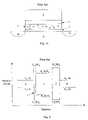
- FIG. 2is an energy band diagram of the SONOS cell of FIGS. 1 a , 1 b , and 1 c.
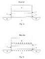
- FIGS. 3 a and 3 bare cross-sectional views illustrating formation of a SONOS-type device according to the present invention.
- Tunneling oxide 3is typically a high quality oxide, but is very thin, while blocking oxide 7 , though thicker, is normally a lower quality oxide and will have flaws.
- a traditional SONOS deviceis of course a SONOS-type device, but the term as used here is intended to be broader.
- the gate electrodeneed not be silicon; it can be either semiconductor or metal, for example, it may comprise tungsten.
- any appropriate materialcan be used for the channel region.
- a SONOS-type devicehas layers having the same functions as the silicon channel region, gate oxide, nitride charge storage layer, blocking oxide, and silicon gate electrode of a traditional SONOS device, but one or more materials can be substituted for the material traditionally used for any of these layers.
- the devicecan be formed on a monocrystalline semiconductor substrate, or on a polysilicon substrate, as a thin film transistor (TFT) array.
- TFTthin film transistor
- this oxidation processcan be followed by an annealing process.
- Any suitable annealing process known in the art that maintains the quality of the oxide layercan be employed in the invention.
- the annealing processis performed in a nitrogen and oxygen atmosphere, such as nitric oxide (NO), to form an oxynitride and improve the quality and reliability of the oxide layer.
- NOnitric oxide
- a SONOS-type device according to the present inventionmay have, for example, a charge storage layer comprising, in order and in contact with each other: a silicon nitride film, an aluminum oxide film, and another silicon nitride film.
Landscapes
- Engineering & Computer Science (AREA)
- Condensed Matter Physics & Semiconductors (AREA)
- Crystallography & Structural Chemistry (AREA)
- General Chemical & Material Sciences (AREA)
- Physics & Mathematics (AREA)
- Chemical Kinetics & Catalysis (AREA)
- Chemical & Material Sciences (AREA)
- General Physics & Mathematics (AREA)
- Manufacturing & Machinery (AREA)
- Computer Hardware Design (AREA)
- Microelectronics & Electronic Packaging (AREA)
- Power Engineering (AREA)
- Non-Volatile Memory (AREA)
- Semiconductor Memories (AREA)
Abstract
Description
Claims (43)
Priority Applications (1)
| Application Number | Priority Date | Filing Date | Title |
|---|---|---|---|
| US10/668,693US7012299B2 (en) | 2003-09-23 | 2003-09-23 | Storage layer optimization of a nonvolatile memory device |
Applications Claiming Priority (1)
| Application Number | Priority Date | Filing Date | Title |
|---|---|---|---|
| US10/668,693US7012299B2 (en) | 2003-09-23 | 2003-09-23 | Storage layer optimization of a nonvolatile memory device |
Publications (2)
| Publication Number | Publication Date |
|---|---|
| US20050062098A1 US20050062098A1 (en) | 2005-03-24 |
| US7012299B2true US7012299B2 (en) | 2006-03-14 |
Family
ID=34313542
Family Applications (1)
| Application Number | Title | Priority Date | Filing Date |
|---|---|---|---|
| US10/668,693Expired - LifetimeUS7012299B2 (en) | 2003-09-23 | 2003-09-23 | Storage layer optimization of a nonvolatile memory device |
Country Status (1)
| Country | Link |
|---|---|
| US (1) | US7012299B2 (en) |
Cited By (39)
| Publication number | Priority date | Publication date | Assignee | Title |
|---|---|---|---|---|
| US20050247970A1 (en)* | 2004-04-23 | 2005-11-10 | Samsung Electronics Co., Ltd., | Memory device including a dielectric multilayer structure and method of fabricating the same |
| US20050285184A1 (en)* | 2004-06-09 | 2005-12-29 | Jung Jin H | Flash memory device and method for programming/erasing the same |
| US20060108610A1 (en)* | 2003-11-14 | 2006-05-25 | Samsung Electronics, Co., Ltd. | Method of manufacturing a thin dielectric layer using a heat treatment and a semiconductor device formed using the method |
| US20060146608A1 (en)* | 2004-12-30 | 2006-07-06 | Matrix Semiconductor, Inc. | Integrated circuit including memory array incorporating multiple types of NAND string structures |
| US20060160303A1 (en)* | 2005-01-20 | 2006-07-20 | Chartered Semiconductor Manufacturing Ltd | Method for forming high-K charge storage device |
| US20060198189A1 (en)* | 2005-01-03 | 2006-09-07 | Macronix International Co., Ltd. | Non-volatile memory cells, memory arrays including the same and methods of operating cells and arrays |
| US20060202252A1 (en)* | 2005-01-03 | 2006-09-14 | Macronix International Co., Ltd. | Non-volatile memory cells, memory arrays including the same and methods of operating cells and arrays |
| US20060273404A1 (en)* | 2005-06-01 | 2006-12-07 | Matrix Semiconductor, Inc. | TFT charge storage memory cell having high-mobility corrugated channel |
| US20060289948A1 (en)* | 2005-06-22 | 2006-12-28 | International Business Machines Corporation | Method to control flatband/threshold voltage in high-k metal gated stacks and structures thereof |
| US20080013355A1 (en)* | 2003-12-18 | 2008-01-17 | Herner S B | Selective oxidation of silicon in diode, tft and monolithic three dimensional memory arrays |
| US20080012065A1 (en)* | 2006-07-11 | 2008-01-17 | Sandisk Corporation | Bandgap engineered charge storage layer for 3D TFT |
| US20080315206A1 (en)* | 2007-06-19 | 2008-12-25 | Herner S Brad | Highly Scalable Thin Film Transistor |
| US20090059676A1 (en)* | 2007-08-27 | 2009-03-05 | Macronix International Co., Ltd. | HIGH-k CAPPED BLOCKING DIELECTRIC BANDGAP ENGINEERED SONOS AND MONOS |
| US20090057752A1 (en)* | 2007-08-28 | 2009-03-05 | Macronix International Co., Ltd. | Non-volatile memory and method for manufacturing the same |
| US20090141555A1 (en)* | 2006-05-05 | 2009-06-04 | Macronix International Co., Ltd. | Method of programming and erasing a p-channel be-sonos nand flash memory |
| US20090152617A1 (en)* | 2007-12-17 | 2009-06-18 | Spansion Llc | Hetero-structure variable silicon richness nitride for mlc flash memory device |
| US20090243001A1 (en)* | 2008-03-31 | 2009-10-01 | Krishnaswamy Ramkumar | Sequential deposition and anneal of a dielectic layer in a charge trapping memory device |
| US20100072539A1 (en)* | 2008-09-22 | 2010-03-25 | Naoki Yasuda | Memory cell of nonvolatile semiconductor memory device |
| US20100123181A1 (en)* | 2008-11-18 | 2010-05-20 | Samsung Electronics Co., Ltd. | Nonvolatile memory devices including multiple charge trapping layers |
| US20100193859A1 (en)* | 2007-08-09 | 2010-08-05 | Macronix International Co., Ltd. | Blocking dielectric engineered charge trapping memory cell with high speed erase |
| US7863128B1 (en)* | 2005-02-04 | 2011-01-04 | Spansion Llc | Non-volatile memory device with improved erase speed |
| US20110101442A1 (en)* | 2009-11-02 | 2011-05-05 | Applied Materials, Inc. | Multi-Layer Charge Trap Silicon Nitride/Oxynitride Layer Engineering with Interface Region Control |
| US20110147825A1 (en)* | 2008-11-18 | 2011-06-23 | Samsung Electronics Co., Ltd. | Nonvolatile memory devices including deep and high density trapping layers |
| US20130163340A1 (en)* | 2011-12-24 | 2013-06-27 | Sandisk Technologies Inc. | Non-volatile storage system with three layer floating gate |
| US8643124B2 (en) | 2007-05-25 | 2014-02-04 | Cypress Semiconductor Corporation | Oxide-nitride-oxide stack having multiple oxynitride layers |
| US8685813B2 (en) | 2012-02-15 | 2014-04-01 | Cypress Semiconductor Corporation | Method of integrating a charge-trapping gate stack into a CMOS flow |
| US8686490B2 (en) | 2006-12-20 | 2014-04-01 | Sandisk Corporation | Electron blocking layers for electronic devices |
| US8940645B2 (en) | 2007-05-25 | 2015-01-27 | Cypress Semiconductor Corporation | Radical oxidation process for fabricating a nonvolatile charge trap memory device |
| US9355849B1 (en) | 2007-05-25 | 2016-05-31 | Cypress Semiconductor Corporation | Oxide-nitride-oxide stack having multiple oxynitride layers |
| US9449980B2 (en) | 2014-10-31 | 2016-09-20 | Sandisk Technologies Llc | Band gap tailoring for a tunneling dielectric for a three-dimensional memory structure |
| US9780108B2 (en) | 2015-10-19 | 2017-10-03 | Sandisk Technologies Llc | Ultrathin semiconductor channel three-dimensional memory devices |
| US9876025B2 (en) | 2015-10-19 | 2018-01-23 | Sandisk Technologies Llc | Methods for manufacturing ultrathin semiconductor channel three-dimensional memory devices |
| US9929240B2 (en) | 2007-05-25 | 2018-03-27 | Cypress Semiconductor Corporation | Memory transistor with multiple charge storing layers and a high work function gate electrode |
| US10374067B2 (en) | 2007-05-25 | 2019-08-06 | Longitude Flash Memory Solutions Ltd. | Oxide-nitride-oxide stack having multiple oxynitride layers |
| US10797060B2 (en) | 2018-12-17 | 2020-10-06 | Sandisk Technologies Llc | Three-dimensional memory device having stressed vertical semiconductor channels and method of making the same |
| US10797061B2 (en) | 2018-12-17 | 2020-10-06 | Sandisk Technologies Llc | Three-dimensional memory device having stressed vertical semiconductor channels and method of making the same |
| US10985172B2 (en) | 2019-01-18 | 2021-04-20 | Sandisk Technologies Llc | Three-dimensional memory device with mobility-enhanced vertical channels and methods of forming the same |
| US11322509B2 (en) | 2018-12-17 | 2022-05-03 | Sandisk Technologies Llc | Three-dimensional memory device including a silicon-germanium source contact layer and method of making the same |
| US11721727B2 (en) | 2018-12-17 | 2023-08-08 | Sandisk Technologies Llc | Three-dimensional memory device including a silicon-germanium source contact layer and method of making the same |
Families Citing this family (37)
| Publication number | Priority date | Publication date | Assignee | Title |
|---|---|---|---|---|
| US7183143B2 (en)* | 2003-10-27 | 2007-02-27 | Macronix International Co., Ltd. | Method for forming nitrided tunnel oxide layer |
| US8482052B2 (en)* | 2005-01-03 | 2013-07-09 | Macronix International Co., Ltd. | Silicon on insulator and thin film transistor bandgap engineered split gate memory |
| US8264028B2 (en)* | 2005-01-03 | 2012-09-11 | Macronix International Co., Ltd. | Non-volatile memory cells, memory arrays including the same and methods of operating cells and arrays |
| US7709334B2 (en)* | 2005-12-09 | 2010-05-04 | Macronix International Co., Ltd. | Stacked non-volatile memory device and methods for fabricating the same |
| US7262095B1 (en)* | 2005-06-07 | 2007-08-28 | Spansion Llc | System and method for reducing process-induced charging |
| US7763927B2 (en) | 2005-12-15 | 2010-07-27 | Macronix International Co., Ltd. | Non-volatile memory device having a nitride-oxide dielectric layer |
| US20070063252A1 (en)* | 2005-09-16 | 2007-03-22 | Yuan Diana D | Non-volatile memory and SRAM based on resonant tunneling devices |
| US7824991B2 (en)* | 2006-01-18 | 2010-11-02 | Macronix International Co., Ltd. | Method for nitridation of the interface between a dielectric and a substrate in a MOS device |
| JP2007194511A (en)* | 2006-01-23 | 2007-08-02 | Renesas Technology Corp | Nonvolatile semiconductor memory device and manufacturing method thereof |
| US7521317B2 (en)* | 2006-03-15 | 2009-04-21 | Freescale Semiconductor, Inc. | Method of forming a semiconductor device and structure thereof |
| KR100717770B1 (en)* | 2006-04-24 | 2007-05-11 | 주식회사 하이닉스반도체 | Flash memory device having a dielectric film having a laminated structure including a zirconium oxide film and a manufacturing method thereof |
| US7746694B2 (en)* | 2006-07-10 | 2010-06-29 | Macronix International Co., Ltd. | Nonvolatile memory array having modified channel region interface |
| US8816422B2 (en)* | 2006-09-15 | 2014-08-26 | Taiwan Semiconductor Manufacturing Company, Ltd. | Multi-trapping layer flash memory cell |
| US8294197B2 (en)* | 2006-09-22 | 2012-10-23 | Taiwan Semiconductor Manufacturing Company, Ltd. | Program/erase schemes for floating gate memory cells |
| US8772858B2 (en)* | 2006-10-11 | 2014-07-08 | Macronix International Co., Ltd. | Vertical channel memory and manufacturing method thereof and operating method using the same |
| US7811890B2 (en) | 2006-10-11 | 2010-10-12 | Macronix International Co., Ltd. | Vertical channel transistor structure and manufacturing method thereof |
| US20080237694A1 (en)* | 2007-03-27 | 2008-10-02 | Michael Specht | Integrated circuit, cell, cell arrangement, method for manufacturing an integrated circuit, method for manufacturing a cell, memory module |
| US9716153B2 (en) | 2007-05-25 | 2017-07-25 | Cypress Semiconductor Corporation | Nonvolatile charge trap memory device having a deuterated layer in a multi-layer charge-trapping region |
| US8680601B2 (en)* | 2007-05-25 | 2014-03-25 | Cypress Semiconductor Corporation | Nonvolatile charge trap memory device having a deuterated layer in a multi-layer charge-trapping region |
| US9299568B2 (en)* | 2007-05-25 | 2016-03-29 | Cypress Semiconductor Corporation | SONOS ONO stack scaling |
| CN101330013B (en)* | 2007-06-21 | 2010-08-11 | 中芯国际集成电路制造(上海)有限公司 | Method for preparing tunneling oxide layer and flash memory |
| US7838923B2 (en)* | 2007-08-09 | 2010-11-23 | Macronix International Co., Ltd. | Lateral pocket implant charge trapping devices |
| US7643349B2 (en)* | 2007-10-18 | 2010-01-05 | Macronix International Co., Ltd. | Efficient erase algorithm for SONOS-type NAND flash |
| US7848148B2 (en)* | 2007-10-18 | 2010-12-07 | Macronix International Co., Ltd. | One-transistor cell semiconductor on insulator random access memory |
| US9431549B2 (en)* | 2007-12-12 | 2016-08-30 | Cypress Semiconductor Corporation | Nonvolatile charge trap memory device having a high dielectric constant blocking region |
| US8068370B2 (en)* | 2008-04-18 | 2011-11-29 | Macronix International Co., Ltd. | Floating gate memory device with interpoly charge trapping structure |
| JP2009272348A (en)* | 2008-04-30 | 2009-11-19 | Toshiba Corp | Semiconductor device and method for manufacturing the same |
| US8735963B2 (en)* | 2008-07-07 | 2014-05-27 | Taiwan Semiconductor Manufacturing Company, Ltd. | Flash memory cells having leakage-inhibition layers |
| US7615439B1 (en)* | 2008-09-29 | 2009-11-10 | Sandisk Corporation | Damascene process for carbon memory element with MIIM diode |
| US7969011B2 (en)* | 2008-09-29 | 2011-06-28 | Sandisk 3D Llc | MIIM diodes having stacked structure |
| US20100078758A1 (en)* | 2008-09-29 | 2010-04-01 | Sekar Deepak C | Miim diodes |
| US8081516B2 (en)* | 2009-01-02 | 2011-12-20 | Macronix International Co., Ltd. | Method and apparatus to suppress fringing field interference of charge trapping NAND memory |
| US8861273B2 (en)* | 2009-04-21 | 2014-10-14 | Macronix International Co., Ltd. | Bandgap engineered charge trapping memory in two-transistor nor architecture |
| US8222688B1 (en) | 2009-04-24 | 2012-07-17 | Cypress Semiconductor Corporation | SONOS stack with split nitride memory layer |
| US9240405B2 (en) | 2011-04-19 | 2016-01-19 | Macronix International Co., Ltd. | Memory with off-chip controller |
| US9559113B2 (en) | 2014-05-01 | 2017-01-31 | Macronix International Co., Ltd. | SSL/GSL gate oxide in 3D vertical channel NAND |
| US9793289B2 (en)* | 2015-06-08 | 2017-10-17 | Toshiba Memory Corporation | Non-volatile memory device |
Citations (6)
| Publication number | Priority date | Publication date | Assignee | Title |
|---|---|---|---|---|
| US20020028541A1 (en)* | 2000-08-14 | 2002-03-07 | Lee Thomas H. | Dense arrays and charge storage devices, and methods for making same |
| US6469343B1 (en)* | 1998-04-02 | 2002-10-22 | Nippon Steel Corporation | Multi-level type nonvolatile semiconductor memory device |
| US6674138B1 (en)* | 2001-12-31 | 2004-01-06 | Advanced Micro Devices, Inc. | Use of high-k dielectric materials in modified ONO structure for semiconductor devices |
| US6677640B1 (en)* | 2000-03-01 | 2004-01-13 | Micron Technology, Inc. | Memory cell with tight coupling |
| US6682973B1 (en)* | 2002-05-16 | 2004-01-27 | Advanced Micro Devices, Inc. | Formation of well-controlled thin SiO, SiN, SiON layer for multilayer high-K dielectric applications |
| US6797604B2 (en)* | 2000-05-08 | 2004-09-28 | International Business Machines Corporation | Method for manufacturing device substrate with metal back-gate and structure formed thereby |
- 2003
- 2003-09-23USUS10/668,693patent/US7012299B2/ennot_activeExpired - Lifetime
Patent Citations (7)
| Publication number | Priority date | Publication date | Assignee | Title |
|---|---|---|---|---|
| US6605839B2 (en)* | 1997-04-25 | 2003-08-12 | Nippon Steel Corporation | Multi-level type nonvolatile semiconductor memory device |
| US6469343B1 (en)* | 1998-04-02 | 2002-10-22 | Nippon Steel Corporation | Multi-level type nonvolatile semiconductor memory device |
| US6677640B1 (en)* | 2000-03-01 | 2004-01-13 | Micron Technology, Inc. | Memory cell with tight coupling |
| US6797604B2 (en)* | 2000-05-08 | 2004-09-28 | International Business Machines Corporation | Method for manufacturing device substrate with metal back-gate and structure formed thereby |
| US20020028541A1 (en)* | 2000-08-14 | 2002-03-07 | Lee Thomas H. | Dense arrays and charge storage devices, and methods for making same |
| US6674138B1 (en)* | 2001-12-31 | 2004-01-06 | Advanced Micro Devices, Inc. | Use of high-k dielectric materials in modified ONO structure for semiconductor devices |
| US6682973B1 (en)* | 2002-05-16 | 2004-01-27 | Advanced Micro Devices, Inc. | Formation of well-controlled thin SiO, SiN, SiON layer for multilayer high-K dielectric applications |
Non-Patent Citations (3)
| Title |
|---|
| Evtukh, A. A. ,et al. , "The Multilayer Silicon Nitride Films as a Media for Charge Storage in MNOS Structures", 1996 Int'l Nonvolatile Memory Technology Conference, (Apr. 1996),pp. 91-93. |
| Govoreanu, B. ,et al. ,"VARIOT: A Novel Multilayer Tunnel Barrier Concept for Low-Voltage Nonvolatile Memory Devices", IEEE Electron Device Letters, 2003, (2003),pp. 1-3. |
| U.S. Appl. No. 10/270,127, filed Oct. 15, 2002, Mahajani et al. |
Cited By (78)
| Publication number | Priority date | Publication date | Assignee | Title |
|---|---|---|---|---|
| US20060108610A1 (en)* | 2003-11-14 | 2006-05-25 | Samsung Electronics, Co., Ltd. | Method of manufacturing a thin dielectric layer using a heat treatment and a semiconductor device formed using the method |
| US7190024B2 (en)* | 2003-11-14 | 2007-03-13 | Samsung Electronics, Co., Ltd. | Method of manufacturing a thin dielectric layer using a heat treatment and a semiconductor device formed using the method |
| US7414274B2 (en) | 2003-12-18 | 2008-08-19 | Sandisk 3D Llp | Selective oxidation of silicon in diode, TFT and monolithic three dimensional memory arrays |
| US20080013355A1 (en)* | 2003-12-18 | 2008-01-17 | Herner S B | Selective oxidation of silicon in diode, tft and monolithic three dimensional memory arrays |
| US20050247970A1 (en)* | 2004-04-23 | 2005-11-10 | Samsung Electronics Co., Ltd., | Memory device including a dielectric multilayer structure and method of fabricating the same |
| US20050285184A1 (en)* | 2004-06-09 | 2005-12-29 | Jung Jin H | Flash memory device and method for programming/erasing the same |
| US7177191B2 (en) | 2004-12-30 | 2007-02-13 | Sandisk 3D Llc | Integrated circuit including memory array incorporating multiple types of NAND string structures |
| US20060146608A1 (en)* | 2004-12-30 | 2006-07-06 | Matrix Semiconductor, Inc. | Integrated circuit including memory array incorporating multiple types of NAND string structures |
| US20060198189A1 (en)* | 2005-01-03 | 2006-09-07 | Macronix International Co., Ltd. | Non-volatile memory cells, memory arrays including the same and methods of operating cells and arrays |
| US20060202252A1 (en)* | 2005-01-03 | 2006-09-14 | Macronix International Co., Ltd. | Non-volatile memory cells, memory arrays including the same and methods of operating cells and arrays |
| US7642585B2 (en) | 2005-01-03 | 2010-01-05 | Macronix International Co., Ltd. | Non-volatile memory cells, memory arrays including the same and methods of operating cells and arrays |
| US7479425B2 (en)* | 2005-01-20 | 2009-01-20 | Chartered Semiconductor Manufacturing, Ltd | Method for forming high-K charge storage device |
| US20060160303A1 (en)* | 2005-01-20 | 2006-07-20 | Chartered Semiconductor Manufacturing Ltd | Method for forming high-K charge storage device |
| US7863128B1 (en)* | 2005-02-04 | 2011-01-04 | Spansion Llc | Non-volatile memory device with improved erase speed |
| US20060273404A1 (en)* | 2005-06-01 | 2006-12-07 | Matrix Semiconductor, Inc. | TFT charge storage memory cell having high-mobility corrugated channel |
| US8946017B2 (en) | 2005-06-01 | 2015-02-03 | Sandisk 3D Llc | Method of making a TFT charge storage memory cell having high-mobility corrugated channel |
| US8110863B2 (en) | 2005-06-01 | 2012-02-07 | Sandisk 3D Llc | TFT charge storage memory cell having high-mobility corrugated channel |
| US20060289948A1 (en)* | 2005-06-22 | 2006-12-28 | International Business Machines Corporation | Method to control flatband/threshold voltage in high-k metal gated stacks and structures thereof |
| US20090141555A1 (en)* | 2006-05-05 | 2009-06-04 | Macronix International Co., Ltd. | Method of programming and erasing a p-channel be-sonos nand flash memory |
| US7839696B2 (en) | 2006-05-05 | 2010-11-23 | Macronix International Co., Ltd. | Method of programming and erasing a p-channel BE-SONOS NAND flash memory |
| US20080012065A1 (en)* | 2006-07-11 | 2008-01-17 | Sandisk Corporation | Bandgap engineered charge storage layer for 3D TFT |
| US9214525B2 (en) | 2006-12-20 | 2015-12-15 | Sandisk Corporation | Gate stack having electron blocking layers on charge storage layers for electronic devices |
| US8686490B2 (en) | 2006-12-20 | 2014-04-01 | Sandisk Corporation | Electron blocking layers for electronic devices |
| US11056565B2 (en) | 2007-05-25 | 2021-07-06 | Longitude Flash Memory Solutions Ltd. | Flash memory device and method |
| US10312336B2 (en) | 2007-05-25 | 2019-06-04 | Cypress Semiconductor Corporation | Memory transistor with multiple charge storing layers and a high work function gate electrode |
| US12266521B2 (en) | 2007-05-25 | 2025-04-01 | Longitude Flash Memory Solutions Ltd. | Oxide-nitride-oxide stack having multiple oxynitride layers |
| US20150187960A1 (en) | 2007-05-25 | 2015-07-02 | Cypress Semiconductor Corporation | Radical Oxidation Process For Fabricating A Nonvolatile Charge Trap Memory Device |
| US10903342B2 (en) | 2007-05-25 | 2021-01-26 | Longitude Flash Memory Solutions Ltd. | Oxide-nitride-oxide stack having multiple oxynitride layers |
| US10903068B2 (en) | 2007-05-25 | 2021-01-26 | Longitude Flash Memory Solutions Ltd. | Oxide-nitride-oxide stack having multiple oxynitride layers |
| US11222965B2 (en) | 2007-05-25 | 2022-01-11 | Longitude Flash Memory Solutions Ltd | Oxide-nitride-oxide stack having multiple oxynitride layers |
| US11456365B2 (en) | 2007-05-25 | 2022-09-27 | Longitude Flash Memory Solutions Ltd. | Memory transistor with multiple charge storing layers and a high work function gate electrode |
| US10896973B2 (en) | 2007-05-25 | 2021-01-19 | Longitude Flash Memory Solutions Ltd. | Oxide-nitride-oxide stack having multiple oxynitride layers |
| US8643124B2 (en) | 2007-05-25 | 2014-02-04 | Cypress Semiconductor Corporation | Oxide-nitride-oxide stack having multiple oxynitride layers |
| US10593812B2 (en) | 2007-05-25 | 2020-03-17 | Longitude Flash Memory Solutions Ltd. | Radical oxidation process for fabricating a nonvolatile charge trap memory device |
| US10446656B2 (en) | 2007-05-25 | 2019-10-15 | Longitude Flash Memory Solutions Ltd. | Memory transistor with multiple charge storing layers and a high work function gate electrode |
| US10374067B2 (en) | 2007-05-25 | 2019-08-06 | Longitude Flash Memory Solutions Ltd. | Oxide-nitride-oxide stack having multiple oxynitride layers |
| US8940645B2 (en) | 2007-05-25 | 2015-01-27 | Cypress Semiconductor Corporation | Radical oxidation process for fabricating a nonvolatile charge trap memory device |
| US11721733B2 (en) | 2007-05-25 | 2023-08-08 | Longitude Flash Memory Solutions Ltd. | Memory transistor with multiple charge storing layers and a high work function gate electrode |
| US11784243B2 (en) | 2007-05-25 | 2023-10-10 | Longitude Flash Memory Solutions Ltd | Oxide-nitride-oxide stack having multiple oxynitride layers |
| US10304968B2 (en) | 2007-05-25 | 2019-05-28 | Cypress Semiconductor Corporation | Radical oxidation process for fabricating a nonvolatile charge trap memory device |
| US12009401B2 (en) | 2007-05-25 | 2024-06-11 | Longitude Flash Memory Solutions Ltd. | Memory transistor with multiple charge storing layers and a high work function gate electrode |
| US9929240B2 (en) | 2007-05-25 | 2018-03-27 | Cypress Semiconductor Corporation | Memory transistor with multiple charge storing layers and a high work function gate electrode |
| US9355849B1 (en) | 2007-05-25 | 2016-05-31 | Cypress Semiconductor Corporation | Oxide-nitride-oxide stack having multiple oxynitride layers |
| US7888205B2 (en) | 2007-06-19 | 2011-02-15 | Sandisk 3D Llc | Highly scalable thin film transistor |
| US20100173457A1 (en)* | 2007-06-19 | 2010-07-08 | Sandisk 3D Llc | Highly scalable thin film transistor |
| US20080315206A1 (en)* | 2007-06-19 | 2008-12-25 | Herner S Brad | Highly Scalable Thin Film Transistor |
| US8343840B2 (en) | 2007-08-09 | 2013-01-01 | Macronix International Co., Ltd. | Blocking dielectric engineered charge trapping memory cell with high speed erase |
| US20100193859A1 (en)* | 2007-08-09 | 2010-08-05 | Macronix International Co., Ltd. | Blocking dielectric engineered charge trapping memory cell with high speed erase |
| US8119481B2 (en) | 2007-08-27 | 2012-02-21 | Macronix International Co., Ltd. | High-κ capped blocking dielectric bandgap engineered SONOS and MONOS |
| US8330210B2 (en) | 2007-08-27 | 2012-12-11 | Macronix International Co., Ltd. | High-κ capped blocking dielectric bandgap engineered SONOS and MONOS |
| US7816727B2 (en)* | 2007-08-27 | 2010-10-19 | Macronix International Co., Ltd. | High-κ capped blocking dielectric bandgap engineered SONOS and MONOS |
| US20110003452A1 (en)* | 2007-08-27 | 2011-01-06 | Macronix International Co., Ltd. | HIGH-k CAPPED BLOCKING DIELECTRIC BANDGAP ENGINEERED SONOS AND MONOS |
| US20090059676A1 (en)* | 2007-08-27 | 2009-03-05 | Macronix International Co., Ltd. | HIGH-k CAPPED BLOCKING DIELECTRIC BANDGAP ENGINEERED SONOS AND MONOS |
| US7772072B2 (en)* | 2007-08-28 | 2010-08-10 | Macronix International Co., Ltd. | Method for manufacturing non-volatile memory |
| US20090057752A1 (en)* | 2007-08-28 | 2009-03-05 | Macronix International Co., Ltd. | Non-volatile memory and method for manufacturing the same |
| US20090152617A1 (en)* | 2007-12-17 | 2009-06-18 | Spansion Llc | Hetero-structure variable silicon richness nitride for mlc flash memory device |
| US7602067B2 (en)* | 2007-12-17 | 2009-10-13 | Spansion Llc | Hetero-structure variable silicon rich nitride for multiple level memory flash memory device |
| US8088683B2 (en) | 2008-03-31 | 2012-01-03 | Cypress Semiconductor Corporation | Sequential deposition and anneal of a dielectic layer in a charge trapping memory device |
| US20090243001A1 (en)* | 2008-03-31 | 2009-10-01 | Krishnaswamy Ramkumar | Sequential deposition and anneal of a dielectic layer in a charge trapping memory device |
| US8030701B2 (en)* | 2008-09-22 | 2011-10-04 | Kabushiki Kaisha Toshiba | Memory cell of nonvolatile semiconductor memory device |
| US20100072539A1 (en)* | 2008-09-22 | 2010-03-25 | Naoki Yasuda | Memory cell of nonvolatile semiconductor memory device |
| US20100123181A1 (en)* | 2008-11-18 | 2010-05-20 | Samsung Electronics Co., Ltd. | Nonvolatile memory devices including multiple charge trapping layers |
| US20110147825A1 (en)* | 2008-11-18 | 2011-06-23 | Samsung Electronics Co., Ltd. | Nonvolatile memory devices including deep and high density trapping layers |
| US8431984B2 (en) | 2008-11-18 | 2013-04-30 | Samsung Electronics Co., Ltd. | Nonvolatile memory devices including deep and high density trapping layers |
| US8426907B2 (en) | 2008-11-18 | 2013-04-23 | Samsung Electronics Co., Ltd. | Nonvolatile memory devices including multiple charge trapping layers |
| US20110101442A1 (en)* | 2009-11-02 | 2011-05-05 | Applied Materials, Inc. | Multi-Layer Charge Trap Silicon Nitride/Oxynitride Layer Engineering with Interface Region Control |
| US9502521B2 (en) | 2009-11-02 | 2016-11-22 | Applied Materials, Inc. | Multi-layer charge trap silicon nitride/oxynitride layer engineering with interface region control |
| US8885404B2 (en)* | 2011-12-24 | 2014-11-11 | Sandisk Technologies Inc. | Non-volatile storage system with three layer floating gate |
| US20130163340A1 (en)* | 2011-12-24 | 2013-06-27 | Sandisk Technologies Inc. | Non-volatile storage system with three layer floating gate |
| US8685813B2 (en) | 2012-02-15 | 2014-04-01 | Cypress Semiconductor Corporation | Method of integrating a charge-trapping gate stack into a CMOS flow |
| US9449980B2 (en) | 2014-10-31 | 2016-09-20 | Sandisk Technologies Llc | Band gap tailoring for a tunneling dielectric for a three-dimensional memory structure |
| US9876025B2 (en) | 2015-10-19 | 2018-01-23 | Sandisk Technologies Llc | Methods for manufacturing ultrathin semiconductor channel three-dimensional memory devices |
| US9780108B2 (en) | 2015-10-19 | 2017-10-03 | Sandisk Technologies Llc | Ultrathin semiconductor channel three-dimensional memory devices |
| US11322509B2 (en) | 2018-12-17 | 2022-05-03 | Sandisk Technologies Llc | Three-dimensional memory device including a silicon-germanium source contact layer and method of making the same |
| US11721727B2 (en) | 2018-12-17 | 2023-08-08 | Sandisk Technologies Llc | Three-dimensional memory device including a silicon-germanium source contact layer and method of making the same |
| US10797061B2 (en) | 2018-12-17 | 2020-10-06 | Sandisk Technologies Llc | Three-dimensional memory device having stressed vertical semiconductor channels and method of making the same |
| US10797060B2 (en) | 2018-12-17 | 2020-10-06 | Sandisk Technologies Llc | Three-dimensional memory device having stressed vertical semiconductor channels and method of making the same |
| US10985172B2 (en) | 2019-01-18 | 2021-04-20 | Sandisk Technologies Llc | Three-dimensional memory device with mobility-enhanced vertical channels and methods of forming the same |
Also Published As
| Publication number | Publication date |
|---|---|
| US20050062098A1 (en) | 2005-03-24 |
Similar Documents
| Publication | Publication Date | Title |
|---|---|---|
| US7012299B2 (en) | Storage layer optimization of a nonvolatile memory device | |
| US20080012065A1 (en) | Bandgap engineered charge storage layer for 3D TFT | |
| US7579646B2 (en) | Flash memory with deep quantum well and high-K dielectric | |
| KR100890040B1 (en) | Nonvolatile memory device having a charge trap layer and method of manufacturing same | |
| US7365389B1 (en) | Memory cell having enhanced high-K dielectric | |
| US8816422B2 (en) | Multi-trapping layer flash memory cell | |
| KR100843229B1 (en) | Flash memory device comprising a charge trap film of a hybrid structure and a manufacturing method thereof | |
| JP4014431B2 (en) | Semiconductor memory device and manufacturing method of semiconductor memory device | |
| TWI584450B (en) | Oxide-nitride-oxide stack with multiple oxynitride layers | |
| US8294200B2 (en) | Non-volatile memory device | |
| TW201724527A (en) | SONOS stacked memory components with separate nitride memory layers and associated fabrication processes | |
| KR100819003B1 (en) | Nonvolatile Memory Device Manufacturing Method | |
| US20080246077A1 (en) | Method of fabricating semiconductor memory device and semiconductor memory device fabricated by the method | |
| JP2002261175A (en) | Nonvolatile semiconductor memory and its manufacturing method | |
| US20050205923A1 (en) | Non-volatile memory device having an asymmetrical gate dielectric layer and method of manufacturing the same | |
| US20090014777A1 (en) | Flash Memory Devices and Methods of Manufacturing the Same | |
| US20090114977A1 (en) | Nonvolatile memory device having charge trapping layer and method for fabricating the same | |
| US20080296743A1 (en) | Semiconductor device and method for fabricating the same | |
| US7294547B1 (en) | SONOS memory cell having a graded high-K dielectric | |
| US7202128B1 (en) | Method of forming a memory device having improved erase speed | |
| JPH06350093A (en) | Method of manufacturing nonvolatile semiconductor memory device | |
| JP2009049409A (en) | Nonvolatile memory device and manufacturing method thereof | |
| US7553720B2 (en) | Non-volatile memory device and fabrication method thereof | |
| KR20080041478A (en) | Nonvolatile memory device having a charge trap layer and method of manufacturing same | |
| US10026745B1 (en) | Semiconductor memory cell structure |
Legal Events
| Date | Code | Title | Description |
|---|---|---|---|
| AS | Assignment | Owner name:MATRIX SEMICONDUCTOR, CALIFORNIA Free format text:ASSIGNMENT OF ASSIGNORS INTEREST;ASSIGNORS:WALKER, ANDREW J.;MAHAJANI, MAITREYEE;CHEN, EN-HSING;REEL/FRAME:014307/0408;SIGNING DATES FROM 20040121 TO 20040204 | |
| STCF | Information on status: patent grant | Free format text:PATENTED CASE | |
| AS | Assignment | Owner name:SANDISK 3D LLC,CALIFORNIA Free format text:MERGER;ASSIGNOR:MATRIX SEMICONDUCTOR, INC.;REEL/FRAME:017544/0769 Effective date:20051020 Owner name:SANDISK 3D LLC, CALIFORNIA Free format text:MERGER;ASSIGNOR:MATRIX SEMICONDUCTOR, INC.;REEL/FRAME:017544/0769 Effective date:20051020 | |
| AS | Assignment | Owner name:SANDISK 3D LLC, CALIFORNIA Free format text:CORRECTIVE ASSIGNMENT TO CORRECT THE CORRECTIVE MERGER TO ADD PAGES TO THE MERGER DOCUMENT PREVIOUSLY RECORDED PREVIOUSLY RECORDED ON REEL 017544 FRAME 0769;ASSIGNOR:MATRIX SEMICONDUCTOR, INC.;REEL/FRAME:018950/0686 Effective date:20051020 Owner name:SANDISK 3D LLC,CALIFORNIA Free format text:CORRECTIVE ASSIGNMENT TO CORRECT THE CORRECTIVE MERGER TO ADD PAGES TO THE MERGER DOCUMENT PREVIOUSLY RECORDED PREVIOUSLY RECORDED ON REEL 017544 FRAME 0769. ASSIGNOR(S) HEREBY CONFIRMS THE MERGER;ASSIGNOR:MATRIX SEMICONDUCTOR, INC.;REEL/FRAME:018950/0686 Effective date:20051020 Owner name:SANDISK 3D LLC, CALIFORNIA Free format text:CORRECTIVE ASSIGNMENT TO CORRECT THE CORRECTIVE MERGER TO ADD PAGES TO THE MERGER DOCUMENT PREVIOUSLY RECORDED PREVIOUSLY RECORDED ON REEL 017544 FRAME 0769. ASSIGNOR(S) HEREBY CONFIRMS THE MERGER;ASSIGNOR:MATRIX SEMICONDUCTOR, INC.;REEL/FRAME:018950/0686 Effective date:20051020 | |
| FPAY | Fee payment | Year of fee payment:4 | |
| FPAY | Fee payment | Year of fee payment:8 | |
| AS | Assignment | Owner name:SANDISK TECHNOLOGIES INC., TEXAS Free format text:ASSIGNMENT OF ASSIGNORS INTEREST;ASSIGNOR:SANDISK 3D LLC.;REEL/FRAME:038300/0665 Effective date:20160324 | |
| AS | Assignment | Owner name:SANDISK TECHNOLOGIES INC., TEXAS Free format text:CORRECTIVE ASSIGNMENT TO CORRECT THE INCORRECT LISTED PATENT NUMBER 8853569 TO THE CORRECT PATENT NUMBER 8883569 PREVIOUSLY RECORDED ON REEL 038300 FRAME 0665. ASSIGNOR(S) HEREBY CONFIRMS THE ASSIGNMENT;ASSIGNOR:SANDISK 3D LLC;REEL/FRAME:038520/0552 Effective date:20160324 | |
| AS | Assignment | Owner name:SANDISK TECHNOLOGIES LLC, TEXAS Free format text:CHANGE OF NAME;ASSIGNOR:SANDISK TECHNOLOGIES INC;REEL/FRAME:038813/0004 Effective date:20160516 | |
| MAFP | Maintenance fee payment | Free format text:PAYMENT OF MAINTENANCE FEE, 12TH YEAR, LARGE ENTITY (ORIGINAL EVENT CODE: M1553) Year of fee payment:12 |