US7011614B2 - Infrared thermopile detector system for semiconductor process monitoring and control - Google Patents
Infrared thermopile detector system for semiconductor process monitoring and controlDownload PDFInfo
- Publication number
- US7011614B2 US7011614B2US10/623,244US62324403AUS7011614B2US 7011614 B2US7011614 B2US 7011614B2US 62324403 AUS62324403 AUS 62324403AUS 7011614 B2US7011614 B2US 7011614B2
- Authority
- US
- United States
- Prior art keywords
- gas
- thermopile detector
- semiconductor process
- output
- thermopile
- Prior art date
- Legal status (The legal status is an assumption and is not a legal conclusion. Google has not performed a legal analysis and makes no representation as to the accuracy of the status listed.)
- Expired - Lifetime, expires
Links
- 238000000034methodMethods0.000titleclaimsabstractdescription129
- 230000008569processEffects0.000titleclaimsabstractdescription98
- 239000004065semiconductorSubstances0.000titleclaimsabstractdescription73
- 238000012544monitoring processMethods0.000titleabstractdescription25
- 238000012545processingMethods0.000claimsdescription21
- 230000005855radiationEffects0.000claimsdescription21
- 239000000463materialSubstances0.000claimsdescription19
- 239000003153chemical reaction reagentSubstances0.000claimsdescription16
- 230000004044responseEffects0.000claimsdescription15
- 238000005201scrubbingMethods0.000claimsdescription13
- 238000002835absorbanceMethods0.000claimsdescription4
- 239000012530fluidSubstances0.000claimsdescription3
- 239000007788liquidSubstances0.000claimsdescription3
- 239000007787solidSubstances0.000claims1
- 239000007789gasSubstances0.000description57
- 230000008054signal transmissionEffects0.000description15
- 238000004519manufacturing processMethods0.000description11
- 238000004140cleaningMethods0.000description8
- 238000010926purgeMethods0.000description8
- 239000006096absorbing agentSubstances0.000description7
- RBFQJDQYXXHULB-UHFFFAOYSA-NarsaneChemical compound[AsH3]RBFQJDQYXXHULB-UHFFFAOYSA-N0.000description7
- 238000001514detection methodMethods0.000description7
- PQDJYEQOELDLCP-UHFFFAOYSA-NtrimethylsilaneChemical compoundC[SiH](C)CPQDJYEQOELDLCP-UHFFFAOYSA-N0.000description6
- 229940094989trimethylsilaneDrugs0.000description6
- 230000003595spectral effectEffects0.000description5
- 238000011144upstream manufacturingMethods0.000description5
- 238000011088calibration curveMethods0.000description4
- 230000009977dual effectEffects0.000description4
- 238000005259measurementMethods0.000description4
- BLRPTPMANUNPDV-UHFFFAOYSA-NSilaneChemical compound[SiH4]BLRPTPMANUNPDV-UHFFFAOYSA-N0.000description3
- 238000010521absorption reactionMethods0.000description3
- 239000000203mixtureSubstances0.000description3
- 230000003647oxidationEffects0.000description3
- 238000007254oxidation reactionMethods0.000description3
- 239000002243precursorSubstances0.000description3
- 238000004886process controlMethods0.000description3
- 238000005070samplingMethods0.000description3
- 229910000077silaneInorganic materials0.000description3
- 231100000331toxicToxicity0.000description3
- 230000002588toxic effectEffects0.000description3
- 238000005200wet scrubbingMethods0.000description3
- XYFCBTPGUUZFHI-UHFFFAOYSA-NPhosphineChemical compoundPXYFCBTPGUUZFHI-UHFFFAOYSA-N0.000description2
- 239000007864aqueous solutionSubstances0.000description2
- 230000005540biological transmissionEffects0.000description2
- 238000005229chemical vapour depositionMethods0.000description2
- 238000000151depositionMethods0.000description2
- 230000008021depositionEffects0.000description2
- 230000000694effectsEffects0.000description2
- 231100001261hazardousToxicity0.000description2
- 238000012806monitoring deviceMethods0.000description2
- 125000002524organometallic groupChemical class0.000description2
- 239000000047productSubstances0.000description2
- 238000001228spectrumMethods0.000description2
- 238000012360testing methodMethods0.000description2
- 231100000627threshold limit valueToxicity0.000description2
- XLYOFNOQVPJJNP-UHFFFAOYSA-NwaterSubstancesOXLYOFNOQVPJJNP-UHFFFAOYSA-N0.000description2
- JBRZTFJDHDCESZ-UHFFFAOYSA-NAsGaChemical compound[As]#[Ga]JBRZTFJDHDCESZ-UHFFFAOYSA-N0.000description1
- WKBOTKDWSSQWDR-UHFFFAOYSA-NBromine atomChemical class[Br]WKBOTKDWSSQWDR-UHFFFAOYSA-N0.000description1
- ZAMOUSCENKQFHK-UHFFFAOYSA-NChlorine atomChemical class[Cl]ZAMOUSCENKQFHK-UHFFFAOYSA-N0.000description1
- 229910001218Gallium arsenideInorganic materials0.000description1
- 238000012369In process controlMethods0.000description1
- 229910004014SiF4Inorganic materials0.000description1
- 230000002378acidificating effectEffects0.000description1
- 238000004458analytical methodMethods0.000description1
- 229910000074antimony hydrideInorganic materials0.000description1
- 238000003491arrayMethods0.000description1
- 229910052785arsenicInorganic materials0.000description1
- RQNWIZPPADIBDY-UHFFFAOYSA-Narsenic atomChemical compound[As]RQNWIZPPADIBDY-UHFFFAOYSA-N0.000description1
- GDTBXPJZTBHREO-UHFFFAOYSA-NbromineChemical classBrBrGDTBXPJZTBHREO-UHFFFAOYSA-N0.000description1
- 229910052794bromiumInorganic materials0.000description1
- 239000006227byproductSubstances0.000description1
- 230000003197catalytic effectEffects0.000description1
- 229910052801chlorineInorganic materials0.000description1
- 239000000460chlorineChemical class0.000description1
- 238000004891communicationMethods0.000description1
- 230000003750conditioning effectEffects0.000description1
- 239000000470constituentSubstances0.000description1
- 238000000354decomposition reactionMethods0.000description1
- 238000005137deposition processMethods0.000description1
- 238000013461designMethods0.000description1
- 238000010586diagramMethods0.000description1
- 238000006073displacement reactionMethods0.000description1
- -1distibineChemical compound0.000description1
- 230000004907fluxEffects0.000description1
- 230000007274generation of a signal involved in cell-cell signalingEffects0.000description1
- 229910000078germaneInorganic materials0.000description1
- 239000000383hazardous chemicalSubstances0.000description1
- 238000010965in-process controlMethods0.000description1
- 238000010978in-process monitoringMethods0.000description1
- 230000003993interactionEffects0.000description1
- 125000002496methyl groupChemical group[H]C([H])([H])*0.000description1
- 238000012986modificationMethods0.000description1
- 230000004048modificationEffects0.000description1
- 230000005693optoelectronicsEffects0.000description1
- 229910000073phosphorus hydrideInorganic materials0.000description1
- 238000012805post-processingMethods0.000description1
- 238000002360preparation methodMethods0.000description1
- 150000004756silanesChemical class0.000description1
- ABTOQLMXBSRXSM-UHFFFAOYSA-Nsilicon tetrafluorideChemical compoundF[Si](F)(F)FABTOQLMXBSRXSM-UHFFFAOYSA-N0.000description1
- 239000008247solid mixtureSubstances0.000description1
- 238000001179sorption measurementMethods0.000description1
- OUULRIDHGPHMNQ-UHFFFAOYSA-NstibaneChemical compound[SbH3]OUULRIDHGPHMNQ-UHFFFAOYSA-N0.000description1
- 239000000126substanceSubstances0.000description1
- 238000010977unit operationMethods0.000description1
- 238000007740vapor depositionMethods0.000description1
Images


Classifications
- H—ELECTRICITY
- H01—ELECTRIC ELEMENTS
- H01L—SEMICONDUCTOR DEVICES NOT COVERED BY CLASS H10
- H01L22/00—Testing or measuring during manufacture or treatment; Reliability measurements, i.e. testing of parts without further processing to modify the parts as such; Structural arrangements therefor
- G—PHYSICS
- G01—MEASURING; TESTING
- G01N—INVESTIGATING OR ANALYSING MATERIALS BY DETERMINING THEIR CHEMICAL OR PHYSICAL PROPERTIES
- G01N21/00—Investigating or analysing materials by the use of optical means, i.e. using sub-millimetre waves, infrared, visible or ultraviolet light
- G01N21/17—Systems in which incident light is modified in accordance with the properties of the material investigated
- G01N21/25—Colour; Spectral properties, i.e. comparison of effect of material on the light at two or more different wavelengths or wavelength bands
- G01N21/31—Investigating relative effect of material at wavelengths characteristic of specific elements or molecules, e.g. atomic absorption spectrometry
- G01N21/35—Investigating relative effect of material at wavelengths characteristic of specific elements or molecules, e.g. atomic absorption spectrometry using infrared light
- G01N21/3504—Investigating relative effect of material at wavelengths characteristic of specific elements or molecules, e.g. atomic absorption spectrometry using infrared light for analysing gases, e.g. multi-gas analysis
- G—PHYSICS
- G01—MEASURING; TESTING
- G01J—MEASUREMENT OF INTENSITY, VELOCITY, SPECTRAL CONTENT, POLARISATION, PHASE OR PULSE CHARACTERISTICS OF INFRARED, VISIBLE OR ULTRAVIOLET LIGHT; COLORIMETRY; RADIATION PYROMETRY
- G01J5/00—Radiation pyrometry, e.g. infrared or optical thermometry
- G01J5/0014—Radiation pyrometry, e.g. infrared or optical thermometry for sensing the radiation from gases, flames
- G—PHYSICS
- G01—MEASURING; TESTING
- G01J—MEASUREMENT OF INTENSITY, VELOCITY, SPECTRAL CONTENT, POLARISATION, PHASE OR PULSE CHARACTERISTICS OF INFRARED, VISIBLE OR ULTRAVIOLET LIGHT; COLORIMETRY; RADIATION PYROMETRY
- G01J5/00—Radiation pyrometry, e.g. infrared or optical thermometry
- G01J5/10—Radiation pyrometry, e.g. infrared or optical thermometry using electric radiation detectors
- G01J5/12—Radiation pyrometry, e.g. infrared or optical thermometry using electric radiation detectors using thermoelectric elements, e.g. thermocouples
- H—ELECTRICITY
- H01—ELECTRIC ELEMENTS
- H01L—SEMICONDUCTOR DEVICES NOT COVERED BY CLASS H10
- H01L21/00—Processes or apparatus adapted for the manufacture or treatment of semiconductor or solid state devices or of parts thereof
- H01L21/67—Apparatus specially adapted for handling semiconductor or electric solid state devices during manufacture or treatment thereof; Apparatus specially adapted for handling wafers during manufacture or treatment of semiconductor or electric solid state devices or components ; Apparatus not specifically provided for elsewhere
- H01L21/67005—Apparatus not specifically provided for elsewhere
- H01L21/67242—Apparatus for monitoring, sorting or marking
- H01L21/67253—Process monitoring, e.g. flow or thickness monitoring
- G—PHYSICS
- G01—MEASURING; TESTING
- G01J—MEASUREMENT OF INTENSITY, VELOCITY, SPECTRAL CONTENT, POLARISATION, PHASE OR PULSE CHARACTERISTICS OF INFRARED, VISIBLE OR ULTRAVIOLET LIGHT; COLORIMETRY; RADIATION PYROMETRY
- G01J5/00—Radiation pyrometry, e.g. infrared or optical thermometry
- G01J5/0003—Radiation pyrometry, e.g. infrared or optical thermometry for sensing the radiant heat transfer of samples, e.g. emittance meter
- G01J5/0007—Radiation pyrometry, e.g. infrared or optical thermometry for sensing the radiant heat transfer of samples, e.g. emittance meter of wafers or semiconductor substrates, e.g. using Rapid Thermal Processing
- G—PHYSICS
- G01—MEASURING; TESTING
- G01J—MEASUREMENT OF INTENSITY, VELOCITY, SPECTRAL CONTENT, POLARISATION, PHASE OR PULSE CHARACTERISTICS OF INFRARED, VISIBLE OR ULTRAVIOLET LIGHT; COLORIMETRY; RADIATION PYROMETRY
- G01J5/00—Radiation pyrometry, e.g. infrared or optical thermometry
- G01J5/02—Constructional details
- G01J5/025—Interfacing a pyrometer to an external device or network; User interface
- Y—GENERAL TAGGING OF NEW TECHNOLOGICAL DEVELOPMENTS; GENERAL TAGGING OF CROSS-SECTIONAL TECHNOLOGIES SPANNING OVER SEVERAL SECTIONS OF THE IPC; TECHNICAL SUBJECTS COVERED BY FORMER USPC CROSS-REFERENCE ART COLLECTIONS [XRACs] AND DIGESTS
- Y10—TECHNICAL SUBJECTS COVERED BY FORMER USPC
- Y10T—TECHNICAL SUBJECTS COVERED BY FORMER US CLASSIFICATION
- Y10T483/00—Tool changing
- Y10T483/16—Tool changing with means to transfer work
Definitions
- This inventionrelates to infrared thermopile systems for semiconductor process monitoring and control, and to a method of monitoring and controlling semiconductor processes using infrared thermopile sensing of conditions in and/or affecting such processes.
- Sensors and monitoring devices used in the semiconductor industrygenerally have two purposes.
- One type of such deviceis used as a safety sensor to warn persons (e.g., personnel operating the semiconductor process equipment or otherwise in proximity to such equipment) of the presence of toxic or otherwise hazardous materials associated with the process in the ambient environment of the process system.
- These safety sensorssometimes termed “life safety sensors,” have lower detection limits consistent with the threshold limit values (TLVs) of the gases and vapors to be detected.
- TLVsthreshold limit values
- an arsine gas safety sensormay have a lower detection limit of 50 parts per billion by volume (ppbv), so that any concentration of arsine that is 50 ppbv or higher will be sensed by the safety sensor device.
- sensors and monitoring deviceshave been used in the semiconductor industry.
- Examplesinclude SiF 4 ultraviolet (UV) emission detectors that are used to provide a signal indicative of the completion of chamber cleaning operations.
- UVultraviolet
- the semiconductor manufacturing fieldcontinues to seek improvements in process monitoring and control.
- the present inventionrelates to infrared thermopile systems for semiconductor process monitoring and control, and to a method of monitoring and controlling semiconductor processes using infrared thermopile sensing of conditions in and/or affecting such processes.
- the present inventionrelates to a semiconductor process system including flow circuitry for flow of a process gas.
- the systemcomprises:
- the inventionin another aspect, relates to a method of operating a semiconductor process including processing of or with a gas, said method comprising sensing concentration of a desired component of said gas with a thermopile detector, generating an output from said thermopile detector indicative of concentration of said selected component of said gas, and controlling one or more conditions in and/or affecting the semiconductor process, in response to said output.
- FIG. 1is a schematic representation of a thermopile detector system.
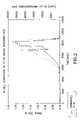
- FIG. 2is a graph of IR cell signal (curve A) and arsine concentration, FT-IR (ppm) (curve B) as a function of time, in seconds, for a thermopile detector in side-by-side service with an FT-IR spectrometer, monitoring arsine breakthrough in the exhaust of a dry scrubber test column.
- FIG. 3is a schematic diagram of a semiconductor process facility, utilizing thermopile detectors for gas phase monitoring and control of process streams associated with a semiconductor process tool and abatement unit.
- FIG. 4is a graph showing the response of a thermopile detector system as a function of different trimethyl silane concentrations.
- FIG. 5is a graph showing a calibration curve for trimethyl silane based on the information depicted in FIG. 4 .
- the present inventionprovides an infrared thermopile detector system useful for semiconductor process monitoring and control, and a method of monitoring and/or controlling semiconductor processes using infrared thermopile sensing of conditions in and/or affecting such processes.
- semiconductor processis intended to be broadly construed to include any and all processing and unit operations involved in the manufacture of semiconductor products, as well as all operations involving treatment or processing of materials used in or produced by a semiconductor manufacturing facility, as well as all operations carried out in connection with the semiconductor manufacturing facility not involving active manufacturing (examples include conditioning of process equipment, purging of chemical delivery lines in preparation for operation, etch cleaning of process tool chambers, abatement of toxic or hazardous gases from effluents produced by the semiconductor manufacturing facility, etc.).
- the operation of the infrared detection system of the inventionis based on the fact that most infrared energy-absorbing molecules absorb infrared radiation at discrete energy levels, so that when a gas, liquid or solid composition is exposed to a broad wavelength infrared radiation, the infrared energy-absorbing component(s) of that composition will absorb a portion of the IR light at very specific wavelengths.
- This phenomenonin turn enables the comparison of the energy spectrum with and without the IR-absorbing component(s), to obtain an absorption profile with patterns that can be used to identify the materials in composition.
- the concentration of a material in the compositionis directly measured by the amount of light that is absorbed by the material.
- IR analyzerswere spectrometers that used grating techniques or prisms to break IR radiation into its individual wavelengths. The individual energies would then be introduced into a gas cell by means of a moveable slit aperture and the radiation of the selected wavelength passing through the gas cell would be detected.
- Such dispersive IR analyzersused electronic processing means to correlate the slit aperture position with the IR energy level and the signal from the detector, and produce energy versus absorbance relations.
- the principal drawbacks of dispersive spectrometersare the use of movable parts that are prone to failure, the cost of the spectrometer apparatus due to the number of components, and the slow collection rates that are characteristic of dispersive spectrometer operation.
- FT-IRFourier transform IR
- dispersive spectrometerslike dispersive spectrometers, also use broad energy IR sources.
- the originally generated IR beamis split into two beams and an interference pattern is created by sending one of the two beams in and out-of-phase, using a movable mirror.
- a laser beamis used to monitor the location of the movable mirror at all times.
- a sensor component of the spectrometer devicereceives the convoluted infrared wave pattern together with the laser-positioning beam. That information is then sent to a computer and deconvoluted using a Fourier transform algorithm.
- the energy versus mirror displacement datais thereby converted into energy versus absorbance relationships.
- the drawbacks of FT-IR spectrometersinclude their complexity and substantial cost.
- thermopile detectorsare employed in the practice of the present invention, and have the major advantages over dispersive and FT-IR spectrometers of (i) low cost, (ii) simplicity of design (no movable parts), (iii) fast response.
- the thermopile-based infrared monitoring system of the inventioncomprises an infrared (IR) light source, a gas cell and a thermopile detector.
- the gas cellis a gas sample monitoring region, which in the broad practice of the invention may comprise any suitable compartment, passageway or chamber in which the gas to be monitored is subjected to passage of IR light through the gas for the purpose of using its IR absorbance-determined output to generate control signal(s) for process monitoring and control.
- the monitoring systemin preferred practice utilizes mirror(s) and/or lenses to collimate and direct the IR light.
- the thermopile detectorgenerates small voltages when exposed to IR light (or heat in the IR spectral regime). The output signal of the thermopile detector is proportional to the incident radiation on the detector.
- Thermopile detectors employed in the preferred practice of the present inventionhave a multiple array of elements in each detector unit.
- one of the thermopile detector elementsis used as a reference, sensing IR light in a range in which substantially no absorption occurs (e.g., wavelength of 4.00 ⁇ 0.02 ⁇ m).
- the second thermopile detector elementis coated with a filter that senses IR energy in the spectral range of interest (such spectral range depending on the particular material to be monitored). Comparison of the differences in the voltages generated by the reference thermopile detector element and those generated by the thermopile detector active element(s) provides a concentration measurement.
- Detectors with up to 4 thermopile detector element arraysare commercially available. For example, in a 4-element detector unit, one detector element is employed as a reference and the remaining 3 detector elements are utilized for measurements in different spectral regions.
- thermopile-based detector systemA schematic representation of a thermopile-based detector system illustrating its operation is shown in FIG. 1 , wherein IR source 10 , such as an IR lamp, generates a broad (extended spectral range of IR wavelengths) infrared beam 12 .
- the IR beam 12is impinged on the gas cell 14 having an interior volume 16 in which the gas to be monitored is present for analysis.
- the gas cellmay be a compartment, cross-sectional region or portion of a gas flow conduit in the semiconductor process system.
- a slip-stream (side stream) of a gas flowmay be extracted from a flow conduit or process tool piping for the gas monitoring operation.
- thermopile detector 20After passage through and interaction with the gas in the interior volume 16 of the gas cell 14 , IR radiation 18 emitting from the gas cell 14 after traversing same then impinges on thermopile detector 20 .
- the thermopile detector unitmay utilize embedded IR filter(s) allowing the radiation of specific IR wavelengths to pass through the (respective) filter(s), in consequence of which the thermopile detector determines the radiation intensity and produces an output voltage signal for each element of the detector.
- central processing unit 24e.g., a personal computer, microprocessor device, or other computational means, wherein voltage signal(s) generated by the detector element(s) are algorithmically manipulated to produce an output concentration value for each of the gas component(s) of interest.
- thermopile-based analyzer systemillustratively shown in FIG. 1 includes mirrors 26 and 28 for focusing the IR radiation. Mirrors can also be used to multipass the infrared beam more than one time across the interior volume 16 in order to enhance the detection limit.
- the infrared light source 10 in the FIG. 1 systemmay be of any suitable type, as for example a PerkinElmer IRL 715 infrared lamp providing IR radiation in a spectrum of from about 2 to about 4.6 ⁇ m wavelength.
- thermopile detector 20likewise may be of any suitable type, as for example a PerkinElmer TPS 3xx single detector, a PerkinElmer TPS 5xx single detector, a PerkinElmer 2534 dual detector, or a PerkinElmer 4339 quad detector, as necessary or desirable in a given end use application of the invention.
- a PerkinElmer TPS 3xx single detectora PerkinElmer TPS 5xx single detector
- a PerkinElmer 2534 dual detectora PerkinElmer 4339 quad detector
- Thermopile detector elements in one preferred embodiment of the inventionhave a response time in the 10–40 millisecond (ms) range.
- Thermopile detector units employed in the practice of the inventionare advantageously configured with detector absorber areas for collecting the infrared light to be measured, with thermal elements positioned below the absorber area, so that infrared light incident on the absorber area heats the absorber area and generates a voltage at the output leads, as a DC voltage providing a direct measure of the incident radiation power.
- Such thermopile detector unitadvantageously employs a gas-specific infrared radiation band pass filter in front of the thermopile detector element, so that the decrease in output voltage generated by such thermopile is directly related to the amount of infrared absorption by the corresponding gas.
- thermopile detector unitmay include a multiplicity of absorber areas, including reference (unfiltered) absorber and gas-filtered absorber regions, with the latter filters being gas-specific for sensing of the semiconductor gases or gas components of interest (e.g., arsine, phosphine, germane, stibine, distibine, silane, substituted silanes, chlorine, bromine, organometallic precursor vapor, etc.).
- reference (unfiltered) absorbere.g., arsine, phosphine, germane, stibine, distibine, silane, substituted silanes, chlorine, bromine, organometallic precursor vapor, etc.
- thermopile IR detector unitsare usefully employed for process control in semiconductor process applications, as described more fully below.
- the thermopile IR detector unitis employed as a gas delivery monitoring unit, e.g., as an in-line monitor installed in the gas delivery line of a semiconductor tool, to ensure delivery of an appropriate concentration of material into the tool chamber and/or flow circuitry.
- a gas delivery monitoring unite.g., as an in-line monitor installed in the gas delivery line of a semiconductor tool
- the inherent stability of the thermopile detector unitfacilitates accurate concentration measurements.
- Use of the thermopile detector unit for such gas delivery sensing and controlin turn minimizes the need to calibrate mass flow controllers used for metered delivery of the feed gas to the tool.
- thermopile detector unitenables feedback control arrangements to be implemented in the semiconductor process, e.g., involving feedback from the thermopile detector unit to the mass flow controller to responsively increase or decrease delivery rates so as to maintain constant concentration, volumetric flow rate, reagent flux, etc.
- thermopile detector unitis utilized as an abatement tool controller for an abatement system for treating effluent produced in a semiconductor manufacturing operation, or other industrial process.
- the thermopile detector unitadvantageously is installed at the inlet of an abatement apparatus, where the abatement apparatus receives the effluent to be treated.
- the thermopile detector unitis used to sense whether or not an upstream tool that generates the effluent in active on-stream operation, is in an active operating mode, or alternatively whether or not the upstream tool is in a non-effluent-producing state, e.g., undergoing purging or cleaning.
- thermopile detector unitby way of specific example, is usefully employed as an abatement tool controller for an effluent scrubber, such as a wet scrubber or a dry scrubber, whereby the presence of the thermopile detector unit transforms the scrubber into a “smart” scrubber and enhances the efficiency of the scrubber, allowing conservation of resources (lower consumables) to be achieved.
- an effluent scrubbersuch as a wet scrubber or a dry scrubber
- thermopile detector unitis useful in an effluent abatement application for facilitating the switching of abatement equipment and/or abatement treatment methods, depending on the type of effluent being discharged from an upstream semiconductor process tool to an effluent abatement scrubber.
- a deposition materiale.g., silane, low-k material
- the effluent gas streamcould be sent by the monitoring and control system to an abatement tool most appropriate for abatement of the effluent from the deposition process (such as a thermal oxidation unit).
- thermopile detector unitWhen the thermopile detector unit does not sense the deposition material, it implies that the tool (e.g., an upstream vapor deposition chamber) is undergoing a cleaning step, and the gas stream then is sent to a different “best available tool” for abatement of the cleaning step effluent (e.g., a water scrubber).
- the toole.g., an upstream vapor deposition chamber
- the gas streamthen is sent to a different “best available tool” for abatement of the cleaning step effluent (e.g., a water scrubber).
- thermopile detector unitis usefully employed as an end point detector, which is installed downstream from a semiconductor process chamber.
- the analyzerserves as an in-line monitor to sense the concentration of species discharged from the process chamber as a function of time. Changes in the sensed concentration of the discharged effluent from the process chamber can be used to generate endpoint signals that can be sent to an tool operator, and/or to automatic process control equipment that responsively shuts down the apparatus or initiates post-processing steps such as purge, cleaning, etc.
- FIG. 2shows measurements collected using a thermopile detector unit in side-by-side service with an FT-IR spectrometer, to monitor arsine breakthrough at the exhaust of a dry scrubber test column.
- the arsine streamwas simulative of the As-containing effluent produced by a semiconductor device structure arsenic doping process, or alternatively by a gallium arsenide epitaxial growth process.
- the thermopile detector unit response(curve A) was faster than the FT-IR spectrometer signal (curve B), and the thermopile detector unit was capable of capturing the concentration changing trends.
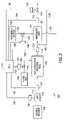
- FIG. 3is schematic representation of an exemplary semiconductor process system 100 , including an illustrative semiconductor process tool 102 coupled with abatement unit 104 for abating effluent components that are of a toxic or hazardous character.
- the systemincludes a central processing unit (CPU) 110 for process monitoring and control utilizing various thermopile detector units, as hereinafter described in greater detail.
- CPUcentral processing unit
- the semiconductor process tool 102is arranged to receive a source reagent from source reagent supply 108 .
- the semiconductor process tool 102may illustratively comprise an epitaxial growth chamber, with the source reagent being a silane gas, or the semiconductor process tool 102 may illustratively comprise a chemical vapor deposition (CVD) chamber receiving an organometallic precursor from the source reagent supply 108 , or the process tool 102 may illustratively comprise any other processing unit in a semiconductor manufacturing facility.
- CVDchemical vapor deposition
- Source reagent from source reagent supply 108flows in feed line 114 to the semiconductor process tool 102 .
- Feed line 114contains a mass flow controller 112 equipped with a mass flow controller set point adjusting unit 138 , coupled to the mass flow controller in operative relationship thereto.
- a thermopile detector unit 116is mounted in an in-line manner in feed line 114 , and arranged for detection of the gaseous reagent flowed to the semiconductor process tool in such feed line 114 .
- the gas concentration signal generated by the thermopile device 116is transmitted in signal transmission line 142 to the CPU 110 .
- the CPU 110may in turn be arranged in controlling relationship, by means of control signal line 140 to the mass flow controller set point adjusting unit 138 , which in turn controls the set point of mass flow controller 112 .
- the set point of the mass flow controllermay be modulated in respect to the concentration sensed by the thermopile detector 116 , to responsively adjust the set point of the mass flow controller by adjusting unit 138 , so that mass flow controller 112 provides a precision set point flow of the source reagent to the semiconductor process tool.
- the semiconductor process tool 102produces an effluent that is flowed in effluent discharge line 118 to the abatement unit 104 for treatment to produce a treated effluent of appropriate character, which is discharged from the abatement unit 104 in abatement unit discharge line 124 .
- the semiconductor process tool effluent discharge line 118 as showncontains a thermopile detector unit 120 mounted therein, for sensing concentration of desired effluent gas component(s).
- the thermopile detector unit 120responsively generates a concentration sensing signal that is transmitted in signal transmission line 154 to CPU 110 .
- the CPU 110can correlatively adjust the set point of mass flow controller 112 , by a modulation of set point adjusting unit 138 .
- the CPU 110in response to the sensed concentration in the effluent discharge stream, as sensed by thermopile detector unit 120 , may terminate flow of source reagent to the semiconductor process tool 102 , such as by closure of a flow control valve (not shown) in feed line 114 , and/or effect other operations that modulate or terminate processing steps involving the semiconductor process tool 102 .
- the effluent gas sensing by thermopile detector unit 120may be employed to effect changeover of the semiconductor process tool 102 from an active processing mode to a cleaning mode, or from a first active processing step to a subsequent processing step.
- the concentration sensed by thermopile detector unit 120 for the component of interest in the effluent stream in discharge line 118may be employed to generate a corresponding concentration signal transmitted in signal transmission line 154 to CPU 110 .
- the concentration signalmay indicate that the active processing step is satisfactory completed.
- the CPU 110then terminates the active flow of source reagent from source reagent supply 108 to the tool, as previously described. Concurrently, the CPU may send a control signal in control signal transmission line 152 to the valve controller 150 .
- the valve controller 150is coupled in controlling relationship to flow control valve 148 in the purge gas feed line 146 connected to purge gas supply 144 .
- the control signal from the CPU 110thereby actuates the valve controller 150 , which in turn causes valve 148 to open, and purge gas to flow through the semiconductor process tool 102 .
- the process toolis efficiently purged of source reagent gases, and readied for subsequent active processing, or alternatively readied for cleaning steps preceding subsequent active (on-stream) processing.
- the purge gashas been flowed through the process tool to sufficient extent to remove the source reagent residues, decomposition by-products, etc., as indicated by corresponding concentration sensing by the thermopile detector unit 120 and transmission of the associated concentration signal in signal transmission line 154 to CPU 110 , the CPU actuates the valve controller 150 to shut valve 148 and terminate purge gas flow to the process tool.
- thermopile detector unit 116in gas feed line 114 to the semiconductor process tool 102
- the systemmay utilize the thermopile detector unit 120 in the effluent discharge line 118 for monitoring and control of the semiconductor process tool 102 .
- thermopile detector unit 120 upstream of abatement unit 104may be constructed and arranged to monitor and responsively control the abatement unit 104 .
- the abatement unit 104 illustratively shown in FIG. 3can be of any of various types, and can include multiple abatement treatment steps and constituent process units, e.g., wet scrubbers, dry scrubbers, thermal oxidation units, catalytic oxidation units, chemisorption units, physical adsorption systems, etc.
- the abatement unit 104is shown in FIG. 3 as comprising a wet scrubbing unit, by means of which the effluent discharged from the semiconductor process tool 102 in discharge line 118 is subjected to wet scrubbing.
- the wet scrubbingis carried out in scrubber abatement unit 104 with a suitable liquid scrubbing medium, e.g., water, acidic aqueous solution, basic aqueous solution, etc., supplied from scrubbing medium source 106 and flowed in scrubbing medium feed line 162 to the abatement unit 104 .
- a suitable liquid scrubbing mediume.g., water, acidic aqueous solution, basic aqueous solution, etc.
- the flow rate of scrubbing medium in line 162is controlled by flow control valve 160 , operatively coupled with valve controller 158 , which in turn is actuated by means of a control signal transmitted via signal transmission line 156 from CPU 110 .
- thermopile detector unit 120therefore is usefully arranged to sense concentration of a component to be abated in the abatement unit 104 , and to responsively transmit a signal correlative of such concentration to CPU 110 in signal transmission line 154 .
- the CPU 110programmatically transmits a control signal in control signal transmission line 156 to valve controller 158 , which modulates the setting of flow control valve 160 to flow a desired amount of scrubbing medium to the abatement unit 104 for contacting with the effluent, to thereby abate the scrubbable component of interest in the effluent stream.
- thermopile detector unit 120will cause the CPU 110 to actuate the valve controller 158 to reduce the flow of scrubbing medium to the abatement unit 104 , so that the scrubbing medium is provided in an amount and at a rate that is appropriate to the amount of scrubbable component to be removed.
- the scrubbing medium containing the scrubbed componentthen is discharged from the abatement unit 104 in scrubbing medium discharge line 130 .
- the treated effluent discharged from abatement unit 104 in effluent discharge line 124may be monitored by thermopile detector unit 126 , which transmits a corresponding concentration signal in signal transmission line 164 to CPU 110 .
- the CPU 110thereupon programmatically responds to the sensed concentration value by modulating the flow control valve 160 via valve controller 158 , as previously described, to increase, maintain or decrease the scrubbing medium flow rate, as necessary to achieve a predetermined low level of scrubbable component in the final effluent discharged from the scrubber abatement unit 104 in discharge line 124 .
- Such predetermined low level of the scrubbable componentmay for example be a concentration that is below the lower detection limit of the thermopile detector unit 126 .
- thermopile detector unit 126may be transmitted to CPU 110 in signal transmission line 164 , to responsively actuate recirculation of effluent from discharge line 124 to the inlet of the abatement unit 104 , in line 128 .
- Line 128is coupled to 3-way valve 132 disposed in discharge line 124 .
- Valve controller 134is operatively coupled with 3-way valve 132 .
- Valve controller 134is joined by control signal transmission line 136 to CPU 110 .
- the CPU 110responsively sends a control signal in signal transmission line 136 to the valve controller 134 coupled with 3-way valve 132 , whereby the valve 132 is adjusted so that treated effluent from discharge line 124 is recirculated in line 128 to line 118 , for reintroduction to abatement unit 104 .
- the recycle rate, as well as the scrubbing medium flow rate,are controllable to maximize removal efficiency of scrubbable components in the abatement unit 104 .
- thermopile detector unitsmay be variously employed in a semiconductor manufacturing facility to monitor gas concentrations and responsively control fluid flow rates and/or other process conditions and/or operational aspects of the semiconductor process, so that process efficiency is maximized, process reagent requirements are minimized, and product consistency is more effectively achieved, relative to a corresponding semiconductor manufacturing facility lacking such thermopile detector monitoring and control means.
- thermopile detectorsmay be advantageously employed, which function to sense the concentrations of multiple gas components in multicomponent process streams.
- thermopile detector unitsmay be utilized concurrently with a multiplicity of detector units in various locations of the semiconductor process, e.g., in specific chambers or regions of the process system flow circuitry, and that the IR thermopile detector units may be integrated with control circuitry involving one or multiple computers, processors, cycle-time program controllers, etc.
- thermopile detectors in producing voltage output signalsmay be utilized with other signal generation and transmission/control devices and interfaces, to effectuate the process monitoring and control functions needed in a specific operation.
- thermopile detector output signalmay be converted to a radio frequency signal transmitted by a radio frequency transponder that is transmitted to a radio frequency receiver in an integrated wireless network for monitoring and control purposes.
- thermopile detectormay be converted to other signal forms, or even reconverted to an infrared control signal for wireless communication to a central processing unit or other computational or control means.
- FIG. 4demonstrates the response of a thermopile detector system as a function of different trimethyl silane concentrations.
- Trimethyl silaneis a candidate material for thermopile-based process monitoring applications as it is used as low-k precursor in semiconductor processes.
- This specific systemincludes a dual sensor thermopile detector.
- the active elementfilters all IR light with the exception of the methyl group (around 3000 cm ⁇ 1).
- the second filtermeasures a narrow band around 2500 cm ⁇ 1 and is used as a reference.
- the curve labeled “TP ratio”depicts the response of the active element divided by the signal generated by the reference element.
- the curve labeled “active”corresponds to the voltage generated by only the active detector element.
- FIG. 4also demonstrates the stability and repeatability of the monitoring system.
- FIG. 5shows a graph of a calibration curve for trimethyl silane, based on the information depicted in FIG. 4 . Similar to FIG. 4 , one calibration curve corresponds to the ratio between the active and reference signals, while the other curve corresponds to the signal generated by the active detector element. The curves were fitted to a second order polynomial with a greater than 0.999 correlation coefficient. Based on such calibration curve, a detection limit of 500 parts per million (ppm) was estimated.
- ppmparts per million
Landscapes
- Physics & Mathematics (AREA)
- General Physics & Mathematics (AREA)
- Spectroscopy & Molecular Physics (AREA)
- Engineering & Computer Science (AREA)
- Power Engineering (AREA)
- Microelectronics & Electronic Packaging (AREA)
- Computer Hardware Design (AREA)
- Manufacturing & Machinery (AREA)
- Chemical & Material Sciences (AREA)
- Life Sciences & Earth Sciences (AREA)
- Pathology (AREA)
- General Health & Medical Sciences (AREA)
- Condensed Matter Physics & Semiconductors (AREA)
- Biochemistry (AREA)
- Analytical Chemistry (AREA)
- Immunology (AREA)
- Health & Medical Sciences (AREA)
- Investigating Or Analysing Materials By Optical Means (AREA)
- Chemical Vapour Deposition (AREA)
- Photometry And Measurement Of Optical Pulse Characteristics (AREA)
- Radiation Pyrometers (AREA)
- Measuring Temperature Or Quantity Of Heat (AREA)
Abstract
Description
- a gas sampling region for the process gas;
- an infrared radiation source constructed and arranged to transmit infrared radiation through the gas sampling region;
- a thermopile detector constructed and arranged to receive infrared radiation after the transmission thereof through the gas sampling region and to responsively generate an output signal correlative of concentration of at least one selected component of the process gas; and
- process control means arranged to receive the output of the thermopile detector and to responsively control one or more process conditions in and/or affecting the semiconductor process system.
Claims (16)
Priority Applications (7)
| Application Number | Priority Date | Filing Date | Title |
|---|---|---|---|
| US10/623,244US7011614B2 (en) | 2002-05-08 | 2003-07-18 | Infrared thermopile detector system for semiconductor process monitoring and control |
| US10/668,489US7129519B2 (en) | 2002-05-08 | 2003-09-23 | Monitoring system comprising infrared thermopile detector |
| US10/731,763US6821795B2 (en) | 2002-05-08 | 2003-12-09 | Infrared thermopile detector system for semiconductor process monitoring and control |
| US10/731,355US7172918B2 (en) | 2002-05-08 | 2003-12-09 | Infrared thermopile detector system for semiconductor process monitoring and control |
| US11/494,193US20060263916A1 (en) | 2002-05-08 | 2006-07-27 | Infrared thermopile detector system for semiconductor process monitoring and control |
| US11/555,094US7351976B2 (en) | 2002-05-08 | 2006-10-31 | Monitoring system comprising infrared thermopile detector |
| US12/060,686US7723685B2 (en) | 2002-05-08 | 2008-04-01 | Monitoring system comprising infrared thermopile detector |
Applications Claiming Priority (2)
| Application Number | Priority Date | Filing Date | Title |
|---|---|---|---|
| US10/140,848US6617175B1 (en) | 2002-05-08 | 2002-05-08 | Infrared thermopile detector system for semiconductor process monitoring and control |
| US10/623,244US7011614B2 (en) | 2002-05-08 | 2003-07-18 | Infrared thermopile detector system for semiconductor process monitoring and control |
Related Parent Applications (1)
| Application Number | Title | Priority Date | Filing Date |
|---|---|---|---|
| US10/140,848DivisionUS6617175B1 (en) | 2002-05-08 | 2002-05-08 | Infrared thermopile detector system for semiconductor process monitoring and control |
Related Child Applications (3)
| Application Number | Title | Priority Date | Filing Date |
|---|---|---|---|
| US10/668,489Continuation-In-PartUS7129519B2 (en) | 2002-05-08 | 2003-09-23 | Monitoring system comprising infrared thermopile detector |
| US10/731,355ContinuationUS7172918B2 (en) | 2002-05-08 | 2003-12-09 | Infrared thermopile detector system for semiconductor process monitoring and control |
| US10/731,763ContinuationUS6821795B2 (en) | 2002-05-08 | 2003-12-09 | Infrared thermopile detector system for semiconductor process monitoring and control |
Publications (2)
| Publication Number | Publication Date |
|---|---|
| US20040018746A1 US20040018746A1 (en) | 2004-01-29 |
| US7011614B2true US7011614B2 (en) | 2006-03-14 |
Family
ID=27788466
Family Applications (6)
| Application Number | Title | Priority Date | Filing Date |
|---|---|---|---|
| US10/140,848Expired - LifetimeUS6617175B1 (en) | 2002-05-08 | 2002-05-08 | Infrared thermopile detector system for semiconductor process monitoring and control |
| US10/623,244Expired - LifetimeUS7011614B2 (en) | 2002-05-08 | 2003-07-18 | Infrared thermopile detector system for semiconductor process monitoring and control |
| US10/731,355Expired - LifetimeUS7172918B2 (en) | 2002-05-08 | 2003-12-09 | Infrared thermopile detector system for semiconductor process monitoring and control |
| US10/731,763Expired - LifetimeUS6821795B2 (en) | 2002-05-08 | 2003-12-09 | Infrared thermopile detector system for semiconductor process monitoring and control |
| US11/494,193AbandonedUS20060263916A1 (en) | 2002-05-08 | 2006-07-27 | Infrared thermopile detector system for semiconductor process monitoring and control |
| US12/060,686Expired - Fee RelatedUS7723685B2 (en) | 2002-05-08 | 2008-04-01 | Monitoring system comprising infrared thermopile detector |
Family Applications Before (1)
| Application Number | Title | Priority Date | Filing Date |
|---|---|---|---|
| US10/140,848Expired - LifetimeUS6617175B1 (en) | 2002-05-08 | 2002-05-08 | Infrared thermopile detector system for semiconductor process monitoring and control |
Family Applications After (4)
| Application Number | Title | Priority Date | Filing Date |
|---|---|---|---|
| US10/731,355Expired - LifetimeUS7172918B2 (en) | 2002-05-08 | 2003-12-09 | Infrared thermopile detector system for semiconductor process monitoring and control |
| US10/731,763Expired - LifetimeUS6821795B2 (en) | 2002-05-08 | 2003-12-09 | Infrared thermopile detector system for semiconductor process monitoring and control |
| US11/494,193AbandonedUS20060263916A1 (en) | 2002-05-08 | 2006-07-27 | Infrared thermopile detector system for semiconductor process monitoring and control |
| US12/060,686Expired - Fee RelatedUS7723685B2 (en) | 2002-05-08 | 2008-04-01 | Monitoring system comprising infrared thermopile detector |
Country Status (8)
| Country | Link |
|---|---|
| US (6) | US6617175B1 (en) |
| EP (1) | EP1502289A4 (en) |
| JP (1) | JP2005526406A (en) |
| KR (1) | KR100958464B1 (en) |
| CN (1) | CN1653588A (en) |
| AU (1) | AU2003276827A1 (en) |
| TW (1) | TWI296141B (en) |
| WO (1) | WO2004010462A2 (en) |
Cited By (10)
| Publication number | Priority date | Publication date | Assignee | Title |
|---|---|---|---|---|
| US20040113080A1 (en)* | 2002-05-08 | 2004-06-17 | Jose Arno | Infrared thermopile detector system for semiconductor process monitoring and control |
| US20060217896A1 (en)* | 2003-03-28 | 2006-09-28 | Advanced Technology Materials, Inc. | Photometrically modulated delivery of reagents |
| US20070200065A1 (en)* | 2002-05-08 | 2007-08-30 | Arno Jose I | Monitoring system comprising infrared thermopile detector |
| US20080006775A1 (en)* | 2006-06-22 | 2008-01-10 | Arno Jose I | Infrared gas detection systems and methods |
| US20080213925A1 (en)* | 2003-03-28 | 2008-09-04 | Advanced Technology Materials, Inc. | Photometrically modulated delivery of reagents |
| US7726876B2 (en) | 2007-03-14 | 2010-06-01 | Entegris, Inc. | System and method for non-intrusive thermal monitor |
| US20100224264A1 (en)* | 2005-06-22 | 2010-09-09 | Advanced Technology Materials, Inc. | Apparatus and process for integrated gas blending |
| DE102013111790A1 (en)* | 2013-10-25 | 2015-04-30 | Aixtron Se | Energy and material consumption optimized CVD reactor |
| US9340878B2 (en) | 2009-05-29 | 2016-05-17 | Entegris, Inc. | TPIR apparatus for monitoring tungsten hexafluoride processing to detect gas phase nucleation, and method and system utilizing same |
| US10895010B2 (en) | 2006-08-31 | 2021-01-19 | Entegris, Inc. | Solid precursor-based delivery of fluid utilizing controlled solids morphology |
Families Citing this family (44)
| Publication number | Priority date | Publication date | Assignee | Title |
|---|---|---|---|---|
| US7080545B2 (en)* | 2002-10-17 | 2006-07-25 | Advanced Technology Materials, Inc. | Apparatus and process for sensing fluoro species in semiconductor processing systems |
| US6927393B2 (en)* | 2002-12-16 | 2005-08-09 | International Business Machines Corporation | Method of in situ monitoring of supercritical fluid process conditions |
| JP3705270B2 (en)* | 2003-01-20 | 2005-10-12 | セイコーエプソン株式会社 | Infrared absorption measurement method, infrared absorption measurement device, and semiconductor device manufacturing method |
| GB0412623D0 (en)* | 2004-06-07 | 2004-07-07 | Boc Group Plc | Method controlling operation of a semiconductor processing system |
| US20060211253A1 (en)* | 2005-03-16 | 2006-09-21 | Ing-Shin Chen | Method and apparatus for monitoring plasma conditions in an etching plasma processing facility |
| DE102005015627A1 (en)* | 2005-04-06 | 2006-10-12 | Carl Zeiss Smt Ag | Optical imaging device |
| US7735452B2 (en) | 2005-07-08 | 2010-06-15 | Mks Instruments, Inc. | Sensor for pulsed deposition monitoring and control |
| US7943204B2 (en) | 2005-08-30 | 2011-05-17 | Advanced Technology Materials, Inc. | Boron ion implantation using alternative fluorinated boron precursors, and formation of large boron hydrides for implantation |
| US7846131B2 (en) | 2005-09-30 | 2010-12-07 | Covidien Ag | Administration feeding set and flow control apparatus with secure loading features |
| US8021336B2 (en) | 2007-01-05 | 2011-09-20 | Tyco Healthcare Group Lp | Pump set for administering fluid with secure loading features and manufacture of component therefor |
| US7722573B2 (en)* | 2006-03-02 | 2010-05-25 | Covidien Ag | Pumping apparatus with secure loading features |
| US7758551B2 (en)* | 2006-03-02 | 2010-07-20 | Covidien Ag | Pump set with secure loading features |
| US7763005B2 (en) | 2006-03-02 | 2010-07-27 | Covidien Ag | Method for using a pump set having secure loading features |
| US7722562B2 (en) | 2006-03-02 | 2010-05-25 | Tyco Healthcare Group Lp | Pump set with safety interlock |
| US7927304B2 (en)* | 2006-03-02 | 2011-04-19 | Tyco Healthcare Group Lp | Enteral feeding pump and feeding set therefor |
| US20090175771A1 (en)* | 2006-03-16 | 2009-07-09 | Applied Materials, Inc. | Abatement of effluent gas |
| WO2007109082A2 (en)* | 2006-03-16 | 2007-09-27 | Applied Materials, Inc. | Methods and apparatus for improving operation of an electronic device manufacturing system |
| CN101400875B (en)* | 2006-03-16 | 2012-11-07 | 应用材料公司 | Method and apparatus for improved operation of an abatement system |
| US7560686B2 (en)* | 2006-12-11 | 2009-07-14 | Tyco Healthcare Group Lp | Pump set and pump with electromagnetic radiation operated interlock |
| CN101678407A (en)* | 2007-05-25 | 2010-03-24 | 应用材料股份有限公司 | Method and apparatus for efficient operation of an abatement system |
| WO2008156687A1 (en)* | 2007-06-15 | 2008-12-24 | Applied Materials, Inc. | Methods and systems for designing and validating operation of abatement systems |
| WO2009055750A1 (en) | 2007-10-26 | 2009-04-30 | Applied Materials, Inc. | Methods and apparatus for smart abatement using an improved fuel circuit |
| KR101755970B1 (en) | 2008-02-11 | 2017-07-07 | 엔테그리스, 아이엔씨. | Method of improving performance and extending lifetime of ion implant system including ion source chamber |
| US8401604B2 (en)* | 2008-04-11 | 2013-03-19 | Glucovista, Llc | Apparatus and methods for non-invasive measurement of a substance within a body |
| US8795225B2 (en)* | 2008-09-29 | 2014-08-05 | Covidien Lp | Fluid detection in an enteral feeding set |
| CN102177576B (en)* | 2008-10-08 | 2013-12-18 | 应用材料公司 | Method and device for detecting idle mode of processing equipment |
| US20110021011A1 (en) | 2009-07-23 | 2011-01-27 | Advanced Technology Materials, Inc. | Carbon materials for carbon implantation |
| US8598022B2 (en) | 2009-10-27 | 2013-12-03 | Advanced Technology Materials, Inc. | Isotopically-enriched boron-containing compounds, and methods of making and using same |
| JP5938350B2 (en)* | 2009-12-09 | 2016-06-22 | コーニンクレッカ フィリップス エヌ ヴェKoninklijke Philips N.V. | Gas measurement module |
| US20110220342A1 (en)* | 2010-03-12 | 2011-09-15 | Applied Materials, Inc. | Methods and apparatus for selectively reducing flow of coolant in a processing system |
| US8154274B2 (en) | 2010-05-11 | 2012-04-10 | Tyco Healthcare Group Lp | Safety interlock |
| US9506804B2 (en) | 2013-01-17 | 2016-11-29 | Detector Electronics Corporation | Open path gas detector |
| DE102013202895A1 (en)* | 2013-02-22 | 2014-08-28 | Zf Friedrichshafen Ag | Multi-speed transmission in planetary construction |
| US20150187562A1 (en)* | 2013-12-27 | 2015-07-02 | Taiwan Semiconductor Manufacturing Company Ltd. | Abatement water flow control system and operation method thereof |
| US10066981B2 (en)* | 2015-04-29 | 2018-09-04 | Kpr U.S., Llc | Detection of malfunction of flow monitoring system of flow control apparatus |
| US9735069B2 (en)* | 2015-09-23 | 2017-08-15 | Lam Research Corporation | Method and apparatus for determining process rate |
| JP2017090351A (en)* | 2015-11-13 | 2017-05-25 | 株式会社堀場製作所 | Radiation thermometer |
| US10586744B2 (en)* | 2017-03-24 | 2020-03-10 | Applied Materials, Inc. | Method for optimizing dry absorber efficiency and lifetime in epitaxial applications |
| SG11202002893PA (en)* | 2017-10-12 | 2020-04-29 | Agency Science Tech & Res | Chemical sensor and method of forming the same |
| US10784174B2 (en) | 2017-10-13 | 2020-09-22 | Lam Research Corporation | Method and apparatus for determining etch process parameters |
| JP7175782B2 (en)* | 2019-01-25 | 2022-11-21 | 株式会社東芝 | Silicon-containing material forming device |
| JP7156605B2 (en)* | 2019-01-25 | 2022-10-19 | 株式会社東芝 | Processing equipment and processing method |
| US12368024B2 (en) | 2021-04-09 | 2025-07-22 | Applied Materials, Inc. | Methods and apparatus for processing a substrate |
| WO2025072547A1 (en)* | 2023-09-29 | 2025-04-03 | Lam Research Corporation | Chemical sensor for automatic flow compensation of mass flow controller |
Citations (11)
| Publication number | Priority date | Publication date | Assignee | Title |
|---|---|---|---|---|
| US4935345A (en) | 1987-04-07 | 1990-06-19 | Arizona Board Of Regents | Implantable microelectronic biochemical sensor incorporating thin film thermopile |
| US5047352A (en) | 1985-05-20 | 1991-09-10 | Arch Development Corporation | Selective chemical detection by energy modulation of sensors |
| US5282473A (en)* | 1992-11-10 | 1994-02-01 | Critikon, Inc. | Sidestream infrared gas analyzer requiring small sample volumes |
| US5464983A (en)* | 1994-04-05 | 1995-11-07 | Industrial Scientific Corporation | Method and apparatus for determining the concentration of a gas |
| US5589689A (en) | 1994-07-07 | 1996-12-31 | Vaisala Oy | Infrared detector with Fabry-Perot interferometer |
| US5650624A (en) | 1995-04-13 | 1997-07-22 | Engelhard Sensor Technologies, Inc. | Passive infrared analysis gas sensor |
| US5721430A (en) | 1995-04-13 | 1998-02-24 | Engelhard Sensor Technologies Inc. | Passive and active infrared analysis gas sensors and applicable multichannel detector assembles |
| US5834777A (en) | 1994-02-14 | 1998-11-10 | Telaire Systems, Inc. | NDIR gas sensor |
| US6348650B1 (en) | 1999-03-24 | 2002-02-19 | Ishizuka Electronics Corporation | Thermopile infrared sensor and process for producing the same |
| US6370950B1 (en)* | 1998-03-20 | 2002-04-16 | Berkin B.V. | Medium flow meter |
| US6469303B1 (en) | 2000-05-17 | 2002-10-22 | Rae Systems, Inc. | Non-dispersive infrared gas sensor |
Family Cites Families (48)
| Publication number | Priority date | Publication date | Assignee | Title |
|---|---|---|---|---|
| US4647777A (en)* | 1985-05-31 | 1987-03-03 | Ametrek, Inc. | Selective gas detector |
| US4859859A (en)* | 1986-12-04 | 1989-08-22 | Cascadia Technology Corporation | Gas analyzers |
| US4816294A (en)* | 1987-05-04 | 1989-03-28 | Midwest Research Institute | Method and apparatus for removing and preventing window deposition during photochemical vapor deposition (photo-CVD) processes |
| US5341214A (en)* | 1989-09-06 | 1994-08-23 | Gaztech International Corporation | NDIR gas analysis using spectral ratioing technique |
| JPH0412525A (en)* | 1990-05-02 | 1992-01-17 | Babcock Hitachi Kk | Chemical vapor growth device for organic metal |
| US5100479A (en)* | 1990-09-21 | 1992-03-31 | The Board Of Regents Acting For And On Behalf Of The University Of Michigan | Thermopile infrared detector with semiconductor supporting rim |
| JPH06317475A (en)* | 1991-07-19 | 1994-11-15 | Terumo Corp | Infrared sensor and manufacturing method thereof |
| US5262645A (en)* | 1991-09-03 | 1993-11-16 | General Motors Corporation | Sensor for measuring alcohol content of alcohol gasoline fuel mixtures |
| US5288649A (en)* | 1991-09-30 | 1994-02-22 | Texas Instruments Incorporated | Method for forming uncooled infrared detector |
| JPH0767151B2 (en)* | 1993-02-25 | 1995-07-19 | 日本電気株式会社 | Infrared imaging device |
| US5646983A (en)* | 1993-03-25 | 1997-07-08 | U.S. Robotics Access Corp. | Host computer digital signal processing system for communicating over voice-grade telephone channels |
| US5436457A (en)* | 1993-06-10 | 1995-07-25 | Horiba, Ltd. | Infrared gas analyzer |
| US5549756A (en)* | 1994-02-02 | 1996-08-27 | Applied Materials, Inc. | Optical pyrometer for a thin film deposition system |
| DE69425817D1 (en)* | 1994-06-04 | 2000-10-12 | Orbisphere Lab | Device and method for luminance analysis |
| JPH08153685A (en)* | 1994-11-25 | 1996-06-11 | Mitsubishi Corp | Special material gas supply device for semiconductors |
| US5649985A (en)* | 1995-11-29 | 1997-07-22 | Kanken Techno Co., Ltd. | Apparatus for removing harmful substances of exhaust gas discharged from semiconductor manufacturing process |
| US5962854A (en) | 1996-06-12 | 1999-10-05 | Ishizuka Electronics Corporation | Infrared sensor and infrared detector |
| US6544193B2 (en)* | 1996-09-04 | 2003-04-08 | Marcio Marc Abreu | Noninvasive measurement of chemical substances |
| US5874736A (en)* | 1996-10-25 | 1999-02-23 | Exergen Corporation | Axillary infrared thermometer and method of use |
| US6122042A (en)* | 1997-02-07 | 2000-09-19 | Wunderman; Irwin | Devices and methods for optically identifying characteristics of material objects |
| JP3233059B2 (en)* | 1997-03-07 | 2001-11-26 | 株式会社村田製作所 | Ultrasonic sensor |
| US5932877A (en)* | 1997-04-17 | 1999-08-03 | Square One Technology, Inc. | High performance side stream infrared gas analyzer |
| US6067840A (en)* | 1997-08-04 | 2000-05-30 | Texas Instruments Incorporated | Method and apparatus for infrared sensing of gas |
| US6444474B1 (en)* | 1998-04-22 | 2002-09-03 | Eltron Research, Inc. | Microfluidic system for measurement of total organic carbon |
| US5967992A (en)* | 1998-06-03 | 1999-10-19 | Trutex, Inc. | Radiometric temperature measurement based on empirical measurements and linear functions |
| JP3699593B2 (en) | 1998-07-07 | 2005-09-28 | 弘昭 杉山 | Cleaning device |
| JP4245714B2 (en) | 1998-12-25 | 2009-04-02 | シーケーディ株式会社 | Exhaust switching device |
| US6396056B1 (en)* | 1999-07-08 | 2002-05-28 | Air Instruments And Measurements, Inc. | Gas detectors and gas analyzers utilizing spectral absorption |
| CA2316059A1 (en)* | 1999-08-24 | 2001-02-24 | Virgilio C. Go Boncan | Methods and compositions for use in cementing in cold environments |
| US7179653B2 (en)* | 2000-03-31 | 2007-02-20 | Showa Denko K.K. | Measuring method for concentration of halogen and fluorine compound, measuring equipment thereof and manufacturing method of halogen compound |
| US6576972B1 (en)* | 2000-08-24 | 2003-06-10 | Heetronix | High temperature circuit structures with expansion matched SiC, AlN and/or AlxGa1-xN(x>0.69) circuit device |
| US6442736B1 (en)* | 2000-10-03 | 2002-08-27 | L'air Liquide Societe Anonyme A Directoire Et Conseil De Surveillance Pour L'etude Et L'expolitation Des Procedes Georges Claude | Semiconductor processing system and method for controlling moisture level therein |
| CN1457423A (en)* | 2001-03-16 | 2003-11-19 | 精工爱普生株式会社 | Infrared detection element and method for fabricating the same and equipment for measuring temperature |
| ATE285256T1 (en)* | 2001-05-11 | 2005-01-15 | Steris Inc | NON-DISPERSIVE INFRARED VAPORIZED HYDROGEN PEROXIDE SENSOR |
| US6616753B2 (en)* | 2001-12-11 | 2003-09-09 | Halliburton Energy Services, Inc. | Methods and compositions for sealing subterranean zones |
| US6828172B2 (en)* | 2002-02-04 | 2004-12-07 | Delphi Technologies, Inc. | Process for a monolithically-integrated micromachined sensor and circuit |
| US7033542B2 (en)* | 2002-02-14 | 2006-04-25 | Archibald William B | High throughput screening with parallel vibrational spectroscopy |
| US20050211555A1 (en)* | 2002-02-14 | 2005-09-29 | Solus Biosystems, Inc. | Method for multiple sample screening using IR spectroscopy |
| DE60221346T2 (en)* | 2002-03-22 | 2008-04-17 | Instrumentarium Corp. | Gas analyzer using thermal sensors |
| US6617175B1 (en)* | 2002-05-08 | 2003-09-09 | Advanced Technology Materials, Inc. | Infrared thermopile detector system for semiconductor process monitoring and control |
| US7129519B2 (en)* | 2002-05-08 | 2006-10-31 | Advanced Technology Materials, Inc. | Monitoring system comprising infrared thermopile detector |
| US20040038442A1 (en)* | 2002-08-26 | 2004-02-26 | Kinsman Larry D. | Optically interactive device packages and methods of assembly |
| TW200407995A (en)* | 2002-11-08 | 2004-05-16 | Nanya Technology Corp | Mark and method for multiple alignment |
| US6989057B2 (en)* | 2002-12-10 | 2006-01-24 | Halliburton Energy Services, Inc. | Zeolite-containing cement composition |
| US6964302B2 (en)* | 2002-12-10 | 2005-11-15 | Halliburton Energy Services, Inc. | Zeolite-containing cement composition |
| US7544640B2 (en)* | 2002-12-10 | 2009-06-09 | Halliburton Energy Services, Inc. | Zeolite-containing treating fluid |
| JP3991018B2 (en)* | 2003-09-01 | 2007-10-17 | シャープ株式会社 | Semiconductor device |
| JP2006275980A (en)* | 2005-03-30 | 2006-10-12 | Denso Corp | Infrared-type gas detector |
- 2002
- 2002-05-08USUS10/140,848patent/US6617175B1/ennot_activeExpired - Lifetime
- 2003
- 2003-04-28TWTW092109889Apatent/TWI296141B/ennot_activeIP Right Cessation
- 2003-05-05JPJP2004522955Apatent/JP2005526406A/enactivePending
- 2003-05-05CNCNA038104504Apatent/CN1653588A/enactivePending
- 2003-05-05WOPCT/US2003/013937patent/WO2004010462A2/enactiveSearch and Examination
- 2003-05-05EPEP03765426Apatent/EP1502289A4/ennot_activeWithdrawn
- 2003-05-05AUAU2003276827Apatent/AU2003276827A1/ennot_activeAbandoned
- 2003-05-05KRKR1020047017524Apatent/KR100958464B1/ennot_activeExpired - Fee Related
- 2003-07-18USUS10/623,244patent/US7011614B2/ennot_activeExpired - Lifetime
- 2003-12-09USUS10/731,355patent/US7172918B2/ennot_activeExpired - Lifetime
- 2003-12-09USUS10/731,763patent/US6821795B2/ennot_activeExpired - Lifetime
- 2006
- 2006-07-27USUS11/494,193patent/US20060263916A1/ennot_activeAbandoned
- 2008
- 2008-04-01USUS12/060,686patent/US7723685B2/ennot_activeExpired - Fee Related
Patent Citations (11)
| Publication number | Priority date | Publication date | Assignee | Title |
|---|---|---|---|---|
| US5047352A (en) | 1985-05-20 | 1991-09-10 | Arch Development Corporation | Selective chemical detection by energy modulation of sensors |
| US4935345A (en) | 1987-04-07 | 1990-06-19 | Arizona Board Of Regents | Implantable microelectronic biochemical sensor incorporating thin film thermopile |
| US5282473A (en)* | 1992-11-10 | 1994-02-01 | Critikon, Inc. | Sidestream infrared gas analyzer requiring small sample volumes |
| US5834777A (en) | 1994-02-14 | 1998-11-10 | Telaire Systems, Inc. | NDIR gas sensor |
| US5464983A (en)* | 1994-04-05 | 1995-11-07 | Industrial Scientific Corporation | Method and apparatus for determining the concentration of a gas |
| US5589689A (en) | 1994-07-07 | 1996-12-31 | Vaisala Oy | Infrared detector with Fabry-Perot interferometer |
| US5650624A (en) | 1995-04-13 | 1997-07-22 | Engelhard Sensor Technologies, Inc. | Passive infrared analysis gas sensor |
| US5721430A (en) | 1995-04-13 | 1998-02-24 | Engelhard Sensor Technologies Inc. | Passive and active infrared analysis gas sensors and applicable multichannel detector assembles |
| US6370950B1 (en)* | 1998-03-20 | 2002-04-16 | Berkin B.V. | Medium flow meter |
| US6348650B1 (en) | 1999-03-24 | 2002-02-19 | Ishizuka Electronics Corporation | Thermopile infrared sensor and process for producing the same |
| US6469303B1 (en) | 2000-05-17 | 2002-10-22 | Rae Systems, Inc. | Non-dispersive infrared gas sensor |
Non-Patent Citations (5)
| Title |
|---|
| Application Note of Thermopile IR Sensors, (Rev.02), Thermometrics Global Business, pp. 1-9, and attachment pages, Sep. 1999. |
| IEEE 100, "The Authoritative Dictionary of IEEE Standards Terms", Seventh Edition ISBN 0-7381-2601-2, page#1174.* |
| Jurgen Schilz, Perkin Elmer Optoelectronics, Applications of Thermoelectric Infrared Sensors (Thermopiles): Gas Detection by Infrared Absorption; NDIR, pp. 1-11. |
| Paul A. Wilks, Wilks Enterprise, "The Birth of Infrared Filometry", Spectroscopy SHOWCASE, Guest Editorial, p. 14, Mar. 2002. |
| Peter Adrian, Sensor Business Digest, Vital Information Publication, Sensor Business Digest Sensor Industry Developments and Trends, Oct. 2001. |
Cited By (21)
| Publication number | Priority date | Publication date | Assignee | Title |
|---|---|---|---|---|
| US20090039266A1 (en)* | 2002-05-08 | 2009-02-12 | Advanced Technology Materials, Inc. | Monitoring system comprising infrared thermopile detector |
| US20040113080A1 (en)* | 2002-05-08 | 2004-06-17 | Jose Arno | Infrared thermopile detector system for semiconductor process monitoring and control |
| US20060263916A1 (en)* | 2002-05-08 | 2006-11-23 | Jose Arno | Infrared thermopile detector system for semiconductor process monitoring and control |
| US7172918B2 (en) | 2002-05-08 | 2007-02-06 | Advanced Technology Materials, Inc. | Infrared thermopile detector system for semiconductor process monitoring and control |
| US20070200065A1 (en)* | 2002-05-08 | 2007-08-30 | Arno Jose I | Monitoring system comprising infrared thermopile detector |
| US7723685B2 (en) | 2002-05-08 | 2010-05-25 | Advanced Technology Materials, Inc. | Monitoring system comprising infrared thermopile detector |
| US7351976B2 (en) | 2002-05-08 | 2008-04-01 | Advanced Technology Materials, Inc. | Monitoring system comprising infrared thermopile detector |
| US7925450B2 (en) | 2003-03-28 | 2011-04-12 | Advanced Technology Materials, Inc. | Photometrically modulated delivery of reagents |
| US8244482B2 (en) | 2003-03-28 | 2012-08-14 | Advanced Technology Materials, Inc. | Photometrically modulated delivery of reagents |
| US7373257B2 (en) | 2003-03-28 | 2008-05-13 | Advanced Technology Materials, Inc. | Photometrically modulated delivery of reagents |
| US7711496B2 (en) | 2003-03-28 | 2010-05-04 | Advanced Technology Materials, Inc. | Photometrically modulated delivery of reagents |
| US20080213925A1 (en)* | 2003-03-28 | 2008-09-04 | Advanced Technology Materials, Inc. | Photometrically modulated delivery of reagents |
| US20100217415A1 (en)* | 2003-03-28 | 2010-08-26 | Advanced Technology Materials, Inc. | Photometrically modulated delivery of reagents |
| US20060217896A1 (en)* | 2003-03-28 | 2006-09-28 | Advanced Technology Materials, Inc. | Photometrically modulated delivery of reagents |
| US9666435B2 (en) | 2005-06-22 | 2017-05-30 | Entegris, Inc. | Apparatus and process for integrated gas blending |
| US20100224264A1 (en)* | 2005-06-22 | 2010-09-09 | Advanced Technology Materials, Inc. | Apparatus and process for integrated gas blending |
| US20080006775A1 (en)* | 2006-06-22 | 2008-01-10 | Arno Jose I | Infrared gas detection systems and methods |
| US10895010B2 (en) | 2006-08-31 | 2021-01-19 | Entegris, Inc. | Solid precursor-based delivery of fluid utilizing controlled solids morphology |
| US7726876B2 (en) | 2007-03-14 | 2010-06-01 | Entegris, Inc. | System and method for non-intrusive thermal monitor |
| US9340878B2 (en) | 2009-05-29 | 2016-05-17 | Entegris, Inc. | TPIR apparatus for monitoring tungsten hexafluoride processing to detect gas phase nucleation, and method and system utilizing same |
| DE102013111790A1 (en)* | 2013-10-25 | 2015-04-30 | Aixtron Se | Energy and material consumption optimized CVD reactor |
Also Published As
| Publication number | Publication date |
|---|---|
| US20040018746A1 (en) | 2004-01-29 |
| WO2004010462A3 (en) | 2004-11-25 |
| US7172918B2 (en) | 2007-02-06 |
| US20090039266A1 (en) | 2009-02-12 |
| EP1502289A2 (en) | 2005-02-02 |
| KR20040108767A (en) | 2004-12-24 |
| US20060263916A1 (en) | 2006-11-23 |
| US20040121494A1 (en) | 2004-06-24 |
| TWI296141B (en) | 2008-04-21 |
| TW200401384A (en) | 2004-01-16 |
| US6617175B1 (en) | 2003-09-09 |
| AU2003276827A1 (en) | 2004-02-09 |
| EP1502289A4 (en) | 2010-01-20 |
| JP2005526406A (en) | 2005-09-02 |
| US7723685B2 (en) | 2010-05-25 |
| KR100958464B1 (en) | 2010-05-17 |
| WO2004010462A2 (en) | 2004-01-29 |
| AU2003276827A8 (en) | 2004-02-09 |
| US20040113080A1 (en) | 2004-06-17 |
| US6821795B2 (en) | 2004-11-23 |
| CN1653588A (en) | 2005-08-10 |
Similar Documents
| Publication | Publication Date | Title |
|---|---|---|
| US7011614B2 (en) | Infrared thermopile detector system for semiconductor process monitoring and control | |
| US7351976B2 (en) | Monitoring system comprising infrared thermopile detector | |
| US9983126B2 (en) | Quantum cascade laser (QCL) based gas sensing system and method | |
| US6442736B1 (en) | Semiconductor processing system and method for controlling moisture level therein | |
| EP2343530B1 (en) | Apparatus for the monitoring and/or controlling of selective catalytic reduction processes | |
| US20070182965A1 (en) | Linked extendable gas observation system for infrared absorption spectroscopy | |
| CN113439202A (en) | Spectroscopic apparatus, system and method for optical sensing of molecular species | |
| US20080006775A1 (en) | Infrared gas detection systems and methods | |
| US20040056196A1 (en) | Method and apparatus for monitoring environment and apparatus for producing semiconductor | |
| US5936250A (en) | Ultraviolet toxic gas point detector | |
| KR102114557B1 (en) | A NDIR analyzer using Two Functional Channels | |
| Mhanna et al. | A cavity-enhanced sensor for benzene detection | |
| JP2001159605A (en) | Laser spectrometer and analysis method | |
| JP4176535B2 (en) | Infrared analyzer | |
| US6917430B2 (en) | Method to improve the control of source chemicals delivery by a carrier gas | |
| WO2018222942A1 (en) | Quantum cascade laser trace-gas detection for in-situ monitoring, process control, and automating end-point determination of chamber clean in semiconductor manufacturing |
Legal Events
| Date | Code | Title | Description |
|---|---|---|---|
| STCF | Information on status: patent grant | Free format text:PATENTED CASE | |
| FEPP | Fee payment procedure | Free format text:PAYOR NUMBER ASSIGNED (ORIGINAL EVENT CODE: ASPN); ENTITY STATUS OF PATENT OWNER: LARGE ENTITY | |
| FPAY | Fee payment | Year of fee payment:4 | |
| FPAY | Fee payment | Year of fee payment:8 | |
| AS | Assignment | Owner name:GOLDMAN SACHS BANK USA, AS COLLATERAL AGENT, NEW YORK Free format text:SECURITY INTEREST;ASSIGNORS:ENTEGRIS, INC.;POCO GRAPHITE, INC.;ATMI, INC.;AND OTHERS;REEL/FRAME:032815/0852 Effective date:20140430 Owner name:GOLDMAN SACHS BANK USA, AS COLLATERAL AGENT, NEW Y Free format text:SECURITY INTEREST;ASSIGNORS:ENTEGRIS, INC.;POCO GRAPHITE, INC.;ATMI, INC.;AND OTHERS;REEL/FRAME:032815/0852 Effective date:20140430 | |
| AS | Assignment | Owner name:GOLDMAN SACHS BANK USA, AS COLLATERAL AGENT, NEW YORK Free format text:SECURITY INTEREST;ASSIGNORS:ENTEGRIS, INC.;POCO GRAPHITE, INC.;ATMI, INC.;AND OTHERS;REEL/FRAME:032812/0192 Effective date:20140430 Owner name:GOLDMAN SACHS BANK USA, AS COLLATERAL AGENT, NEW Y Free format text:SECURITY INTEREST;ASSIGNORS:ENTEGRIS, INC.;POCO GRAPHITE, INC.;ATMI, INC.;AND OTHERS;REEL/FRAME:032812/0192 Effective date:20140430 | |
| AS | Assignment | Owner name:ENTEGRIS, INC., MASSACHUSETTS Free format text:ASSIGNMENT OF ASSIGNORS INTEREST;ASSIGNOR:ADVANCED TECHNOLOGY MATERIALS, INC.;REEL/FRAME:034894/0025 Effective date:20150204 | |
| MAFP | Maintenance fee payment | Free format text:PAYMENT OF MAINTENANCE FEE, 12TH YEAR, LARGE ENTITY (ORIGINAL EVENT CODE: M1553) Year of fee payment:12 | |
| AS | Assignment | Owner name:POCO GRAPHITE, INC., MASSACHUSETTS Free format text:RELEASE BY SECURED PARTY;ASSIGNOR:GOLDMAN SACHS BANK USA, AS COLLATERAL AGENT;REEL/FRAME:047477/0032 Effective date:20181106 Owner name:ATMI PACKAGING, INC., CONNECTICUT Free format text:RELEASE BY SECURED PARTY;ASSIGNOR:GOLDMAN SACHS BANK USA, AS COLLATERAL AGENT;REEL/FRAME:047477/0032 Effective date:20181106 Owner name:ADVANCED TECHNOLOGY MATERIALS, INC., CONNECTICUT Free format text:RELEASE BY SECURED PARTY;ASSIGNOR:GOLDMAN SACHS BANK USA, AS COLLATERAL AGENT;REEL/FRAME:047477/0032 Effective date:20181106 Owner name:ENTEGRIS, INC., MASSACHUSETTS Free format text:RELEASE BY SECURED PARTY;ASSIGNOR:GOLDMAN SACHS BANK USA, AS COLLATERAL AGENT;REEL/FRAME:047477/0032 Effective date:20181106 Owner name:ATMI, INC., CONNECTICUT Free format text:RELEASE BY SECURED PARTY;ASSIGNOR:GOLDMAN SACHS BANK USA, AS COLLATERAL AGENT;REEL/FRAME:047477/0032 Effective date:20181106 Owner name:ATMI, INC., CONNECTICUT Free format text:RELEASE BY SECURED PARTY;ASSIGNOR:GOLDMAN SACHS BANK USA, AS COLLATERAL AGENT;REEL/FRAME:047477/0151 Effective date:20181106 Owner name:ADVANCED TECHNOLOGY MATERIALS, INC., CONNECTICUT Free format text:RELEASE BY SECURED PARTY;ASSIGNOR:GOLDMAN SACHS BANK USA, AS COLLATERAL AGENT;REEL/FRAME:047477/0151 Effective date:20181106 Owner name:ATMI PACKAGING, INC., CONNECTICUT Free format text:RELEASE BY SECURED PARTY;ASSIGNOR:GOLDMAN SACHS BANK USA, AS COLLATERAL AGENT;REEL/FRAME:047477/0151 Effective date:20181106 Owner name:ENTEGRIS, INC., MASSACHUSETTS Free format text:RELEASE BY SECURED PARTY;ASSIGNOR:GOLDMAN SACHS BANK USA, AS COLLATERAL AGENT;REEL/FRAME:047477/0151 Effective date:20181106 Owner name:POCO GRAPHITE, INC., MASSACHUSETTS Free format text:RELEASE BY SECURED PARTY;ASSIGNOR:GOLDMAN SACHS BANK USA, AS COLLATERAL AGENT;REEL/FRAME:047477/0151 Effective date:20181106 | |
| AS | Assignment | Owner name:GOLDMAN SACHS BANK USA, NEW YORK Free format text:SECURITY INTEREST;ASSIGNORS:ENTEGRIS, INC.;SAES PURE GAS, INC.;REEL/FRAME:048811/0679 Effective date:20181106 | |
| AS | Assignment | Owner name:MORGAN STANLEY SENIOR FUNDING, INC., MARYLAND Free format text:ASSIGNMENT OF PATENT SECURITY INTEREST RECORDED AT REEL/FRAME 048811/0679;ASSIGNOR:GOLDMAN SACHS BANK USA;REEL/FRAME:050965/0035 Effective date:20191031 | |
| AS | Assignment | Owner name:TRUIST BANK, AS NOTES COLLATERAL AGENT, NORTH CAROLINA Free format text:SECURITY INTEREST;ASSIGNORS:ENTEGRIS, INC.;ENTEGRIS GP, INC.;POCO GRAPHITE, INC.;AND OTHERS;REEL/FRAME:060613/0072 Effective date:20220706 |