US7009444B1 - Temperature stable voltage reference circuit using a metal-silicon Schottky diode for low voltage circuit applications - Google Patents
Temperature stable voltage reference circuit using a metal-silicon Schottky diode for low voltage circuit applicationsDownload PDFInfo
- Publication number
- US7009444B1 US7009444B1US10/770,233US77023304AUS7009444B1US 7009444 B1US7009444 B1US 7009444B1US 77023304 AUS77023304 AUS 77023304AUS 7009444 B1US7009444 B1US 7009444B1
- Authority
- US
- United States
- Prior art keywords
- voltage
- silicon
- schottky diode
- metal
- current
- Prior art date
- Legal status (The legal status is an assumption and is not a legal conclusion. Google has not performed a legal analysis and makes no representation as to the accuracy of the status listed.)
- Expired - Lifetime, expires
Links
- 229910052710siliconInorganic materials0.000titleclaimsabstractdescription117
- 239000010703siliconSubstances0.000titleclaimsabstractdescription117
- XUIMIQQOPSSXEZ-UHFFFAOYSA-NSiliconChemical compound[Si]XUIMIQQOPSSXEZ-UHFFFAOYSA-N0.000claimsabstractdescription42
- 229910052751metalInorganic materials0.000claimsabstractdescription9
- 239000002184metalSubstances0.000claimsabstractdescription9
- 239000003990capacitorSubstances0.000claimsdescription26
- 229910008479TiSi2Inorganic materials0.000claimsdescription3
- DFJQEGUNXWZVAH-UHFFFAOYSA-Nbis($l^{2}-silanylidene)titaniumChemical compound[Si]=[Ti]=[Si]DFJQEGUNXWZVAH-UHFFFAOYSA-N0.000claimsdescription3
- 230000004888barrier functionEffects0.000abstractdescription8
- 230000000295complement effectEffects0.000description7
- 239000004065semiconductorSubstances0.000description7
- 238000000034methodMethods0.000description4
- 230000008569processEffects0.000description3
- 230000007423decreaseEffects0.000description1
- 230000001419dependent effectEffects0.000description1
- 238000010586diagramMethods0.000description1
- 230000007246mechanismEffects0.000description1
- 150000002739metalsChemical class0.000description1
- 230000003071parasitic effectEffects0.000description1
- 229910021332silicideInorganic materials0.000description1
- FVBUAEGBCNSCDD-UHFFFAOYSA-Nsilicide(4-)Chemical compound[Si-4]FVBUAEGBCNSCDD-UHFFFAOYSA-N0.000description1
- 239000000758substrateSubstances0.000description1
- 229910021350transition metal silicideInorganic materials0.000description1
Images


Classifications
- G—PHYSICS
- G05—CONTROLLING; REGULATING
- G05F—SYSTEMS FOR REGULATING ELECTRIC OR MAGNETIC VARIABLES
- G05F3/00—Non-retroactive systems for regulating electric variables by using an uncontrolled element, or an uncontrolled combination of elements, such element or such combination having self-regulating properties
- G05F3/02—Regulating voltage or current
- G05F3/08—Regulating voltage or current wherein the variable is DC
- G05F3/10—Regulating voltage or current wherein the variable is DC using uncontrolled devices with non-linear characteristics
- G05F3/16—Regulating voltage or current wherein the variable is DC using uncontrolled devices with non-linear characteristics being semiconductor devices
- G05F3/20—Regulating voltage or current wherein the variable is DC using uncontrolled devices with non-linear characteristics being semiconductor devices using diode- transistor combinations
- G05F3/30—Regulators using the difference between the base-emitter voltages of two bipolar transistors operating at different current densities
Definitions
- the present inventionrelates to the field of voltage reference circuits.
- the present inventionrelates to circuits and methods for providing a voltage reference that uses a metal-silicon Schottky diode for the Complementary proportional To Absolute Temperature (CTAT) voltage source that is added to a properly amplified PTAT voltage source to form a temperature stable voltage reference for low voltage applications.
- CTATComplementary proportional To Absolute Temperature
- a bandgap voltage referenceis a voltage reference approximately equal to the bandgap potential (VG 0 ) of the semiconductor at zero degrees Kelvin.
- the bandgap voltage reference circuitis often configured by adding two voltages together: one that is inversely or Complementary proportional To Absolute Temperature (CTAT), and one that is Proportional To Absolute Temperature (PTAT).
- CTATComplementary proportional To Absolute Temperature
- PTATProportional To Absolute Temperature
- the CTAT voltage sourceis typically the base-emitter voltage (VBE) of a diode-connected bipolar transistor.
- FIG. 5illustrates a plot of the base-emitter voltage (VBE) represented on the vertical axis as a function of absolute temperature in degrees Kelvin represented on the horizontal axis.
- the slope of the base-emitter voltage VBE versus temperatureis dependent on the current density through the bipolar transistor. For example, approximate line 501 represents the VBE versus temperature function when the current density is relatively low; approximate line 502 represents the VBE versus temperature function when the current density is moderate; and approximate line 503 represents the VBE versus temperature function when the current density is relatively high.
- the base-emitter voltage (VBE) at zero degrees Kelvini.e., the Y-intercept of FIG. 5
- VBEbase-emitter voltage
- VG 0the bandgap of the semiconductor at zero degrees Kelvin
- VBEVGO - V T ⁇ L ⁇ ⁇ N ⁇ ( I O I D ) ( 1 )
- VBEbase-emitter voltage
- the PTAT voltage(VPTAT, in this case ⁇ VBE) is multiplied by a constant G.
- the resultis added to the CTAT voltage (VCTAT, in this case VBE) to obtain the output voltage VOUT.
- the constant Gis chosen to make the slope of G•VPTAT versus temperature equal in magnitude but opposite in sign to the slope of VCTAT versus temperature. This yields a voltage VOUT which is substantially independent of temperature as depicted in FIG. 7 , and is approximately equal to the bandgap potential of the semiconductor.
- FIG. 8schematically illustrates a conventional circuit 800 that produces the relationship described by Equation 4.
- This conventional circuit 800is especially employed in Silicon CMOS processes in which parasitic PNP bipolar transistors are available having a substrate that serves as the collector.
- the conventional circuit 800includes two bipolar transistors 801 and 802 .
- the current density J 1 passing through bipolar transistor 801is equal to the current I 1 divided by its emitter area A 1 .
- the current density J 2 passing through bipolar transistor 802is equal to the current I 2 divided by its emitter area A 2 .
- the voltage at the emitter terminal of bipolar transistor 801i.e., VBE(J 1 )
- the voltage at the emitter terminal of bipolar transistor 802i.e., VBE(J 2 )
- the amplifier 803has gain G. Accordingly, a voltage of G•(VBE(J 1 ) ⁇ VBE(J 2 )) is applied at the output terminal of the amplifier 803 .
- the output voltage VOUTis obtained by summing 807 the output voltage of the amplifier 803 with the base-emitter voltage of the bipolar transistor 801 .
- the currents I 1 and I 2 , and the emitter areas A 1 and A 2are chosen such that the voltage VBE(J 1 ) at the emitter terminal of bipolar transistor 801 is larger than the emitter voltage VBE(J 2 ) at the emitter terminal of bipolar transistor 802 and such that the difference in base emitter voltages (i.e., VBE(J 1 ) minus VBE(J 2 )) is significantly larger than the offset voltage of the amplifier 803 .
- the current sources 805 and 806 used to bias the respective bipolar transistors 801 and 802are typically generated using the output voltage VOUT of the bandgap reference circuit 800 . If the supply voltage does not affect the currents through either bipolar transistor, the output voltage is independent of the supply voltage as well as temperature for higher supply voltages.
- the bipolar transistors 801 and 802should be carefully matched. Matching of devices is quite difficult. Minor and yet inevitable spatial process variations often cause some mismatch between common devices.
- FIG. 9schematically illustrates an alternative bandgap voltage reference circuit 900 along with an associated timing diagram 910 .
- the bandgap voltage reference circuit 900only uses one bipolar transistor 901 . Accordingly, there is no matching issue between two bipolar transistors as there is with the bandgap voltage reference circuit 800 of FIG. 8 . Furthermore, power consumption is reduced since there is only one bipolar transistor drawing current.
- the bandgap voltage reference 900requires a low frequency clock signal ⁇ 1 , and a non-overlapping complement, ⁇ 2 .
- a higher current I 1is passed through the bipolar transistor 901 creating a higher base-emitter voltage VBE(J 1 ) which is sampled and stored on capacitor C 1 .
- J 1is the current density through the bipolar transistor 901 when the total current is I 1 .
- a lower current I 2is placed through the bipolar transistor 902 generating a lower base-emitter voltage VBE(J 2 ) which is sampled and stored on capacitor C 2 .
- the difference between these two voltagesis multiplied by a specific gain G using an amplifier 903 .
- the amplified voltageis then added to the higher VBE voltage.
- the amplifier gain Gis chosen such that the resulting output voltage VOUT is a constant with respect to temperature.
- Each of these conventional bandgap voltage reference circuits 800 and 900are effective in generating a bandgap voltage reference that is approximately equal to the bandgap potential of the underlying semiconductor as long as the high supply voltage is sufficiently high for the amplifiers 803 and 903 to generate voltages below and approaching the bandgap potential (1.2 volts in the case of silicon). Accordingly, as supply voltages drop to and below 1.2 volts, the performance of circuits 800 and 900 will degrade. With lower voltage applications becoming more prevalent, voltage references that are lower than the bandgap potential of the semiconductor may be useful.
- silicon-based voltage reference circuitsthat provide voltage references that are relatively independent of temperature and below the bandgap potential of silicon. It would especially be advantageous if such reference circuits may operate with lower supply voltages.
- the principles of the present inventionare directed towards silicon-based voltage reference circuits that, contrary to conventional silicon-based bandgap voltage reference circuits, generate a relatively temperature and power supply independent voltage references that are less than even the bandgap potential of silicon.
- the silicon-based voltage reference circuitincludes a metal-silicon Schottky diode.
- a current sourcesupplies a current through the metal-silicon Schottky diode.
- the anode terminal of the Schottky diodeis a Complementary proportional To Absolute Temperature (CTAT) voltage source.
- CTATComplementary proportional To Absolute Temperature
- the anode terminalhas a voltage at zero degrees Kelvin of approximately the barrier height of the metal-silicon Schottky diode, which is less than the bandgap potential for silicon for most selections of metal.
- the voltage reference circuitalso includes a Proportional To Absolute Temperature (PTAT) voltage source that generates a PTAT voltage that has a slope with temperature that is approximately equal to, but opposite in sign, to the CTAT voltage.
- PTATProportional To Absolute Temperature
- This PTAT voltagemay be generated in a variety of ways, conventional or otherwise.
- a summeradds the CTAT voltage to the PTAT voltage to generate the temperature stable reference voltage that is less than the bandgap voltage of silicon.
- FIG. 1schematically illustrates a silicon-based voltage reference that uses a biased metal-silicon Schottky diode to generate a Complementary proportional To Absolute Temperature (CTAT) voltage in accordance with the principles of the present invention
- FIG. 2Aillustrates an embodiment of the Proportional To Absolute Temperature (PTAT) voltage source of FIG. 1 in which a voltage differential across two metal-silicon Schottky diodes including the metal-silicon Schottky diode of FIG. 1 is used as the PTAT voltage;
- PTATProportional To Absolute Temperature
- FIG. 2Billustrates an alternative embodiment of the PTAT voltage source of FIG. 1 in which different base-emitter voltages of two bipolar transistors are used as the PTAT voltage;
- FIG. 2Cillustrates an alternative embodiment of the PTAT voltage source of FIG. 1 in which a single bipolar transistor provides the differential base-emitter voltage for use as the PTAT voltage;
- FIG. 3illustrates an embodiment of the silicon-based voltage reference circuit of FIG. 1 in which the anode voltage of the Schottky diode is sampled at different times to provide the CTAT and PTAT voltages;
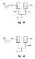
- FIG. 4Aillustrates a first embodiment of the current source of FIG. 3 ;
- FIG. 4Billustrates a second embodiment of the current source of FIG. 3 ;
- FIG. 5illustrates the known physical relationships between a base-emitter voltage, temperature, and current density
- FIG. 6illustrates the known physical relationships between the difference in base-emitter voltages due to different current densities at different temperatures
- FIG. 7illustrates the addition of a CTAT voltage to a PTAT voltage to generate a voltage that is relatively stable with temperature
- FIG. 8illustrates a conventional bandgap voltage reference in which two bipolar transistors with different current densities are used to generate both the CTAT and PTAT voltages.
- FIG. 9illustrates a conventional bandgap voltage reference in which a single bipolar transistor with different current densities sampled at different times is used to generate both the CTAT and PTAT voltages.
- the principles of the present inventionare directed towards silicon-based voltage reference circuits that, contrary to conventional silicon-based bandgap voltage reference circuits, generate temperature stable voltage references that are less than the bandgap potential of silicon, and that may operate with supply voltages that are less than the silicon bandgap potential.
- FIG. 1schematically illustrates a silicon-based voltage reference 100 that uses a biased metal-silicon Schottky diode 101 to generate a Complementary proportional To Absolute Temperature (CTAT) voltage in accordance with the principles of the present invention.
- a current source 102supplies a current I through the metal-silicon Schottky diode 101 .
- the anode terminal 103 of the metal-silicon Schottky diode 101is a Complementary proportional To Absolute Temperature (CTAT) voltage source.
- CTATComplementary proportional To Absolute Temperature
- the anode terminal 103has a voltage at zero degrees Kelvin at the barrier height of the metal-silicon Schottky diode. The barrier height depends on the metal chosen.
- the “metal” in a metal-silicon Schottky diodemay include any metal or even metal silicide.
- TiSi2is a transition metal silicide that may be used to obtain a barrier height of approximately 0.6V.
- the choice of metalis not limited to TiSi2 as there are many metals having a barrier height that is below the bandgap potential of silicon.
- the voltage reference circuitalso includes a Proportional To Absolute Temperature (PTAT) voltage source 104 that generates a PTAT voltage that has a positive slope with temperature that is approximately equal to the negative slope with temperature of the CTAT voltage at the node terminal 103 .
- the PTAT voltage 103may be generated in a variety of ways. The principles of the present invention are not restricted to the manner in which the PTAT voltage is generated.
- a summer 105adds the CTAT voltage to the PTAT voltage to generate the temperature stable reference voltage VOUT that is less than the bandgap voltage of silicon.
- the PTAT voltage source 104may be any mechanism for generating a PTAT voltage. However, for illustrative purposes, three examples of PTAT voltage sources will be described with respect to FIGS. 2A through 2C .
- FIG. 2Aillustrates an embodiment 204 A of the PTAT voltage source 104 of FIG. 1 .
- the PTAT voltage source 204 Auses a voltage differential across the anode voltage of two metal-silicon Schottky diodes (including the metal-silicon Schottky diode 101 ) of FIG. 1 .
- the PTAT voltage source 204 Aincludes a second metal-silicon Schottky diode 201 A.
- a second current source 202 Ais configured during operation to supply a current through the second metal-silicon Schottky diode 201 A to a low voltage supply (such as ground) such that the second metal-silicon Schottky diode 201 A has a current density that is different than the current density passing through the first metal-silicon Schottky diode 101 .
- An amplifier 206 Ahas a negative input terminal that is coupled to the anode terminal 203 A of the second metal-silicon Schottky diode, and a positive input terminal that is coupled to the anode terminal 103 of the first metal-silicon Schottky diode 101 .
- the voltage differential between two metal-silicon Schottky diodesis a PTAT voltage.
- the amplifier 206 Aamplifies this voltage as appropriate to generate another PTAT voltage that has a positive slope with temperature that is equal in magnitude to the slope with temperature of the CTAT voltage present at the anode terminal 103 of the first metal-silicon Schottky diode.
- FIG. 2Billustrates a second embodiment 204 B of the PTAT voltage source 104 of FIG. 1 .
- the PTAT voltage source 204 Buses a voltage differential between base-emitter voltages of two bipolar transistors as a PTAT voltage.
- the PTAT voltage source 204 Bincludes two bipolar transistors 201 B and 202 B.
- a current source 203 Bis configured during operation to provide a current I 2 through the base-emitter interface of the bipolar transistor 201 B such that the base-emitter terminal of the bipolar transistor 201 B has a certain current density.
- a current source 208 Bis configured during operation to provide a current I 3 through the base-emitter interface of the bipolar transistor 202 B such that the base-emitter terminal of the bipolar transistor 202 B has a current density that is different than the current density of the first bipolar transistor 201 B.
- An amplifier 207 Bhas a negative input terminal that is coupled to the emitter terminal 205 B of the bipolar transistor 201 B, and a positive input terminal that is coupled to the emitter terminal 206 B of the second bipolar transistor 202 B.
- the voltage differential between the emitter voltages of the two bipolar transistorsis a PTAT voltage.
- the amplifier 207 Bamplifies this voltage as appropriate to generate another PTAT voltage that has a positive slope with temperature that is equal in magnitude to the slope with temperature of the CTAT voltage present at the anode terminal 103 of the first metal-silicon Schottky diode.
- FIG. 2Cillustrates a third embodiment 204 C of the PTAT voltage source of FIG. 1 .
- the PTAT voltage source 204 Cuses a single bipolar transistor 201 C to provide the differential base-emitter voltage for use as the PTAT voltage.
- the PTAT voltage source 204 Cincludes a single a bipolar transistor 201 C.
- An alternating current source 202 Cis configured to supply a current through the base-emitter interface of the bipolar transistor during a first time period such that the base-emitter terminal of the bipolar transistor 201 C has a certain current density during that time period.
- the alternating current source 202 Cis also configured to supply a current through the bipolar transistor during a second time period that is non-overlapping with the first time period such that the base-emitter terminal of the bipolar transistor 201 C has a different current density during the second time period.
- a capacitor 205 Cis configured to sample a voltage at the base-emitter terminal 203 C of the bipolar transistor 201 C during the first time period through switch 208 C.
- a second capacitor 206 Cis configured to sample a voltage at the base-emitter terminal of the bipolar transistor 201 C during the second time period through switch 209 C.
- An amplifier 207 Chas a negative input terminal coupled to the second capacitor 206 C so as to receive the voltage sampled by the second capacitor 206 C, and a positive input terminal coupled to the first capacitor 205 C so as to receive the voltage sampled by the first capacitor 205 C.
- the voltage differential between the emitter voltages of the bipolar transistors sampled while experiencing different current densitiesis a PTAT voltage.
- the amplifier 207 Camplifies this voltage as appropriate to generate another PTAT voltage that has a positive slope with temperature that is equal in magnitude to the slope with temperature of the CTAT voltage present at the anode terminal 103 of the first metal-silicon Schottky diode.
- FIG. 3illustrates an embodiment 300 of the silicon-based voltage reference circuit 100 of FIG. 1 in which the anode voltage of the Schottky diode is sampled at different times to provide the CTAT and PTAT voltages.
- the metal-silicon Schottky diode 301 and the summer 305may be similar as described above for the metal-silicon Schottky diode 101 and the summer 105 of FIG. 1 .
- the current source 302is specially configured as an alternating current source to supply a current through the metal-silicon Schottky diode 301 during a first time period (e.g., when clock signal ⁇ 1 is high) such that the anode/cathode interface of the metal-silicon Schottky diode 301 has a first current density during that time period.
- the alternating current source 302also supplies a different current through the metal-silicon Schottky diode during a second time period that is non-overlapping with the first time period (e.g., when clock signal ( 12 is high) such that the metal-silicon interface of the metal-silicon Schottky diode 301 has a different current density during that second time period.
- a first capacitor 306is configured to sample a voltage at the anode terminal 303 of the metal-silicon Schottky diode 301 during the first time period through the switch 309 .
- a second capacitor 307is configured to sample a voltage at the anode terminal 303 of the metal-silicon Schottky diode 301 during the second time period through the switch 310 .
- An amplifier 308has a negative input terminal coupled to the second capacitor 307 so as to receive the voltage sampled by the second capacitor, and a positive input terminal coupled to the first capacitor 306 so as to receive the voltage sampled by the first capacitor.
- the summer 305sums the voltage at the output terminal of the amplifier 308 (which is a PTAT voltage), with the voltage at the positive input terminal of the amplifier (which is a CTAT voltage) to generate the output voltage.
- FIGS. 4A and 4BTwo examples are illustrated in FIGS. 4A and 4B .
- FIG. 4Aillustrates an alternating current source 402 A that includes a first switch 403 A that is configured to be closed during the first time period (when signal ⁇ 1 is high), and a second switch 404 A that is configured to be closed during the second time period (when signal ⁇ 2 is high).
- a current source 405 Asupplies a current through the metal-silicon Schottky diode such that the metal-silicon Schottky diode has the first current density.
- a current source 406 Asupplies a current through the metal-silicon Schottky diode such that the metal-silicon Schottky diode a different current density.
- FIG. 4Billustrates an alternating current source 402 B that includes a current source 405 B configured to supply a current through the metal-silicon Schottky diode such that the metal-silicon Schottky diode has a first current density.
- a second current source 406 Bis configured when the switch 404 B is closed to supply additional current through the metal-silicon Schottky diode such that the metal-silicon Schottky diode has a third current density, wherein the first current density added to the third current density is equal to the second current density.
- All of the embodiments described hereinuse the node voltage of the metal-silicon Schottky diode as the CTAT voltage source.
- the value of this voltage at zero degrees Kelvinis just the barrier height of the metal-silicon barrier, which is most often below the bandgap potential of silicon.
- the resultis a temperature stable voltage reference that may be below the bandgap potential of silicon. Accordingly, the principles of the present invention are suitable for low voltage application in which low, but yet temperature stable, reference voltages are useful, and in which supply voltages may be low as well. Furthermore, this may be done using silicon, arguably one of the most well understood semiconductors.
- the silicon-based voltage reference 300 of FIG. 3is particular useful in that a single silicon-metal Schottky diode 301 is used. This is particularly advantageous as device matching can be even more difficult for Schottky diodes than for bipolar transistors. Furthermore, since only one Schottky diode draws current, and since lower supply voltages may be used, power requirements are reduced.
Landscapes
- Engineering & Computer Science (AREA)
- Microelectronics & Electronic Packaging (AREA)
- Physics & Mathematics (AREA)
- Power Engineering (AREA)
- Nonlinear Science (AREA)
- Electromagnetism (AREA)
- General Physics & Mathematics (AREA)
- Radar, Positioning & Navigation (AREA)
- Automation & Control Theory (AREA)
- Electrodes Of Semiconductors (AREA)
Abstract
Description
- IDis the diode current;
- IOis a process and geometry specific current approximately twenty orders of magnitude higher than the diode reverse saturation current, IS, for the semiconductor (IOis usually significantly higher than the diode current ID);
- VTis the thermal voltage which is equal to kT/q, where k is the well-known Boltzmann constant, T is absolute temperature, and q is the well-known charge of an electron.
- where J1 and J2are the respective current densities flowing through the emitters of the transistors, and is equal to the current flowing through the emitter IEdivided by the emitter area AE.
VOUT=VCTAT+G·VPTAT (3)
and also by the following Equation 4:
VOUT=VBE(J1)+G·[VBE(J1)−VBE(J2)] (4)
Claims (11)
Priority Applications (1)
| Application Number | Priority Date | Filing Date | Title |
|---|---|---|---|
| US10/770,233US7009444B1 (en) | 2004-02-02 | 2004-02-02 | Temperature stable voltage reference circuit using a metal-silicon Schottky diode for low voltage circuit applications |
Applications Claiming Priority (1)
| Application Number | Priority Date | Filing Date | Title |
|---|---|---|---|
| US10/770,233US7009444B1 (en) | 2004-02-02 | 2004-02-02 | Temperature stable voltage reference circuit using a metal-silicon Schottky diode for low voltage circuit applications |
Publications (1)
| Publication Number | Publication Date |
|---|---|
| US7009444B1true US7009444B1 (en) | 2006-03-07 |
Family
ID=35966257
Family Applications (1)
| Application Number | Title | Priority Date | Filing Date |
|---|---|---|---|
| US10/770,233Expired - LifetimeUS7009444B1 (en) | 2004-02-02 | 2004-02-02 | Temperature stable voltage reference circuit using a metal-silicon Schottky diode for low voltage circuit applications |
Country Status (1)
| Country | Link |
|---|---|
| US (1) | US7009444B1 (en) |
Cited By (41)
| Publication number | Priority date | Publication date | Assignee | Title |
|---|---|---|---|---|
| US20080136470A1 (en)* | 2004-03-25 | 2008-06-12 | Nathan Moyal | Method and circuit for rapid alignment of signals |
| US20080258759A1 (en)* | 2007-04-17 | 2008-10-23 | Cypress Semiconductor Corporation | Universal digital block interconnection and channel routing |
| US20090039949A1 (en)* | 2007-08-09 | 2009-02-12 | Giovanni Pietrobon | Method and apparatus for producing a low-noise, temperature-compensated bandgap voltage reference |
| US20100093291A1 (en)* | 2006-04-24 | 2010-04-15 | Embabi Sherif H K | Current controlled biasing for current-steering based rf variable gain amplifiers |
| US7761845B1 (en) | 2002-09-09 | 2010-07-20 | Cypress Semiconductor Corporation | Method for parameterizing a user module |
| US7765095B1 (en) | 2000-10-26 | 2010-07-27 | Cypress Semiconductor Corporation | Conditional branching in an in-circuit emulation system |
| US7770113B1 (en) | 2001-11-19 | 2010-08-03 | Cypress Semiconductor Corporation | System and method for dynamically generating a configuration datasheet |
| US7774190B1 (en) | 2001-11-19 | 2010-08-10 | Cypress Semiconductor Corporation | Sleep and stall in an in-circuit emulation system |
| US7825688B1 (en) | 2000-10-26 | 2010-11-02 | Cypress Semiconductor Corporation | Programmable microcontroller architecture(mixed analog/digital) |
| US7844437B1 (en) | 2001-11-19 | 2010-11-30 | Cypress Semiconductor Corporation | System and method for performing next placements and pruning of disallowed placements for programming an integrated circuit |
| US8026739B2 (en) | 2007-04-17 | 2011-09-27 | Cypress Semiconductor Corporation | System level interconnect with programmable switching |
| US8040266B2 (en) | 2007-04-17 | 2011-10-18 | Cypress Semiconductor Corporation | Programmable sigma-delta analog-to-digital converter |
| US8049569B1 (en) | 2007-09-05 | 2011-11-01 | Cypress Semiconductor Corporation | Circuit and method for improving the accuracy of a crystal-less oscillator having dual-frequency modes |
| US8067948B2 (en) | 2006-03-27 | 2011-11-29 | Cypress Semiconductor Corporation | Input/output multiplexer bus |
| US8069405B1 (en) | 2001-11-19 | 2011-11-29 | Cypress Semiconductor Corporation | User interface for efficiently browsing an electronic document using data-driven tabs |
| US8069428B1 (en) | 2001-10-24 | 2011-11-29 | Cypress Semiconductor Corporation | Techniques for generating microcontroller configuration information |
| US8078970B1 (en) | 2001-11-09 | 2011-12-13 | Cypress Semiconductor Corporation | Graphical user interface with user-selectable list-box |
| US8078894B1 (en) | 2007-04-25 | 2011-12-13 | Cypress Semiconductor Corporation | Power management architecture, method and configuration system |
| US8085067B1 (en) | 2005-12-21 | 2011-12-27 | Cypress Semiconductor Corporation | Differential-to-single ended signal converter circuit and method |
| US8085100B2 (en) | 2005-02-04 | 2011-12-27 | Cypress Semiconductor Corporation | Poly-phase frequency synthesis oscillator |
| US8089461B2 (en) | 2005-06-23 | 2012-01-03 | Cypress Semiconductor Corporation | Touch wake for electronic devices |
| US8092083B2 (en) | 2007-04-17 | 2012-01-10 | Cypress Semiconductor Corporation | Temperature sensor with digital bandgap |
| US8103497B1 (en) | 2002-03-28 | 2012-01-24 | Cypress Semiconductor Corporation | External interface for event architecture |
| US8103496B1 (en) | 2000-10-26 | 2012-01-24 | Cypress Semicondutor Corporation | Breakpoint control in an in-circuit emulation system |
| US8120408B1 (en) | 2005-05-05 | 2012-02-21 | Cypress Semiconductor Corporation | Voltage controlled oscillator delay cell and method |
| US8130025B2 (en)* | 2007-04-17 | 2012-03-06 | Cypress Semiconductor Corporation | Numerical band gap |
| US8149048B1 (en) | 2000-10-26 | 2012-04-03 | Cypress Semiconductor Corporation | Apparatus and method for programmable power management in a programmable analog circuit block |
| US8176296B2 (en) | 2000-10-26 | 2012-05-08 | Cypress Semiconductor Corporation | Programmable microcontroller architecture |
| US8264214B1 (en) | 2011-03-18 | 2012-09-11 | Altera Corporation | Very low voltage reference circuit |
| US8402313B1 (en) | 2002-05-01 | 2013-03-19 | Cypress Semiconductor Corporation | Reconfigurable testing system and method |
| US8499270B1 (en) | 2007-04-25 | 2013-07-30 | Cypress Semiconductor Corporation | Configuration of programmable IC design elements |
| US8516025B2 (en) | 2007-04-17 | 2013-08-20 | Cypress Semiconductor Corporation | Clock driven dynamic datapath chaining |
| US8533677B1 (en) | 2001-11-19 | 2013-09-10 | Cypress Semiconductor Corporation | Graphical user interface for dynamically reconfiguring a programmable device |
| CN105099439A (en)* | 2014-05-12 | 2015-11-25 | 瑞昱半导体股份有限公司 | Clock pulse generation circuit and method |
| US9448964B2 (en) | 2009-05-04 | 2016-09-20 | Cypress Semiconductor Corporation | Autonomous control in a programmable system |
| TWI558095B (en)* | 2014-05-05 | 2016-11-11 | 瑞昱半導體股份有限公司 | Clock generation circuit and method thereof |
| US9564902B2 (en) | 2007-04-17 | 2017-02-07 | Cypress Semiconductor Corporation | Dynamically configurable and re-configurable data path |
| US9720805B1 (en) | 2007-04-25 | 2017-08-01 | Cypress Semiconductor Corporation | System and method for controlling a target device |
| US10013013B1 (en) | 2017-09-26 | 2018-07-03 | Nxp B.V. | Bandgap voltage reference |
| US10698662B2 (en) | 2001-11-15 | 2020-06-30 | Cypress Semiconductor Corporation | System providing automatic source code generation for personalization and parameterization of user modules |
| US11530954B2 (en)* | 2018-08-01 | 2022-12-20 | Skyworks Solutions, Inc. | On-chip temperature sensor circuits |
Citations (9)
| Publication number | Priority date | Publication date | Assignee | Title |
|---|---|---|---|---|
| US4956567A (en)* | 1989-02-13 | 1990-09-11 | Texas Instruments Incorporated | Temperature compensated bias circuit |
| US5955793A (en)* | 1998-02-11 | 1999-09-21 | Therm-O-Disc, Incorporated | High sensitivity diode temperature sensor with adjustable current source |
| US6052020A (en) | 1997-09-10 | 2000-04-18 | Intel Corporation | Low supply voltage sub-bandgap reference |
| US6184743B1 (en) | 1998-11-12 | 2001-02-06 | International Business Machines Corporation | Bandgap voltage reference circuit without bipolar transistors |
| US6489835B1 (en) | 2001-08-28 | 2002-12-03 | Lattice Semiconductor Corporation | Low voltage bandgap reference circuit |
| US6529066B1 (en) | 2000-02-28 | 2003-03-04 | National Semiconductor Corporation | Low voltage band gap circuit and method |
| US6531857B2 (en) | 2000-11-09 | 2003-03-11 | Agere Systems, Inc. | Low voltage bandgap reference circuit |
| US6642778B2 (en) | 2001-03-13 | 2003-11-04 | Ion E. Opris | Low-voltage bandgap reference circuit |
| US6737848B2 (en)* | 2001-11-15 | 2004-05-18 | Texas Instruments Incorporated | Reference voltage source |
- 2004
- 2004-02-02USUS10/770,233patent/US7009444B1/ennot_activeExpired - Lifetime
Patent Citations (9)
| Publication number | Priority date | Publication date | Assignee | Title |
|---|---|---|---|---|
| US4956567A (en)* | 1989-02-13 | 1990-09-11 | Texas Instruments Incorporated | Temperature compensated bias circuit |
| US6052020A (en) | 1997-09-10 | 2000-04-18 | Intel Corporation | Low supply voltage sub-bandgap reference |
| US5955793A (en)* | 1998-02-11 | 1999-09-21 | Therm-O-Disc, Incorporated | High sensitivity diode temperature sensor with adjustable current source |
| US6184743B1 (en) | 1998-11-12 | 2001-02-06 | International Business Machines Corporation | Bandgap voltage reference circuit without bipolar transistors |
| US6529066B1 (en) | 2000-02-28 | 2003-03-04 | National Semiconductor Corporation | Low voltage band gap circuit and method |
| US6531857B2 (en) | 2000-11-09 | 2003-03-11 | Agere Systems, Inc. | Low voltage bandgap reference circuit |
| US6642778B2 (en) | 2001-03-13 | 2003-11-04 | Ion E. Opris | Low-voltage bandgap reference circuit |
| US6489835B1 (en) | 2001-08-28 | 2002-12-03 | Lattice Semiconductor Corporation | Low voltage bandgap reference circuit |
| US6737848B2 (en)* | 2001-11-15 | 2004-05-18 | Texas Instruments Incorporated | Reference voltage source |
Cited By (62)
| Publication number | Priority date | Publication date | Assignee | Title |
|---|---|---|---|---|
| US8736303B2 (en) | 2000-10-26 | 2014-05-27 | Cypress Semiconductor Corporation | PSOC architecture |
| US7825688B1 (en) | 2000-10-26 | 2010-11-02 | Cypress Semiconductor Corporation | Programmable microcontroller architecture(mixed analog/digital) |
| US9843327B1 (en) | 2000-10-26 | 2017-12-12 | Cypress Semiconductor Corporation | PSOC architecture |
| US8176296B2 (en) | 2000-10-26 | 2012-05-08 | Cypress Semiconductor Corporation | Programmable microcontroller architecture |
| US8555032B2 (en) | 2000-10-26 | 2013-10-08 | Cypress Semiconductor Corporation | Microcontroller programmable system on a chip with programmable interconnect |
| US10261932B2 (en) | 2000-10-26 | 2019-04-16 | Cypress Semiconductor Corporation | Microcontroller programmable system on a chip |
| US8358150B1 (en) | 2000-10-26 | 2013-01-22 | Cypress Semiconductor Corporation | Programmable microcontroller architecture(mixed analog/digital) |
| US7765095B1 (en) | 2000-10-26 | 2010-07-27 | Cypress Semiconductor Corporation | Conditional branching in an in-circuit emulation system |
| US10725954B2 (en) | 2000-10-26 | 2020-07-28 | Monterey Research, Llc | Microcontroller programmable system on a chip |
| US9766650B2 (en) | 2000-10-26 | 2017-09-19 | Cypress Semiconductor Corporation | Microcontroller programmable system on a chip with programmable interconnect |
| US10020810B2 (en) | 2000-10-26 | 2018-07-10 | Cypress Semiconductor Corporation | PSoC architecture |
| US8149048B1 (en) | 2000-10-26 | 2012-04-03 | Cypress Semiconductor Corporation | Apparatus and method for programmable power management in a programmable analog circuit block |
| US8103496B1 (en) | 2000-10-26 | 2012-01-24 | Cypress Semicondutor Corporation | Breakpoint control in an in-circuit emulation system |
| US10248604B2 (en) | 2000-10-26 | 2019-04-02 | Cypress Semiconductor Corporation | Microcontroller programmable system on a chip |
| US8793635B1 (en) | 2001-10-24 | 2014-07-29 | Cypress Semiconductor Corporation | Techniques for generating microcontroller configuration information |
| US10466980B2 (en) | 2001-10-24 | 2019-11-05 | Cypress Semiconductor Corporation | Techniques for generating microcontroller configuration information |
| US8069428B1 (en) | 2001-10-24 | 2011-11-29 | Cypress Semiconductor Corporation | Techniques for generating microcontroller configuration information |
| US8078970B1 (en) | 2001-11-09 | 2011-12-13 | Cypress Semiconductor Corporation | Graphical user interface with user-selectable list-box |
| US10698662B2 (en) | 2001-11-15 | 2020-06-30 | Cypress Semiconductor Corporation | System providing automatic source code generation for personalization and parameterization of user modules |
| US7774190B1 (en) | 2001-11-19 | 2010-08-10 | Cypress Semiconductor Corporation | Sleep and stall in an in-circuit emulation system |
| US7844437B1 (en) | 2001-11-19 | 2010-11-30 | Cypress Semiconductor Corporation | System and method for performing next placements and pruning of disallowed placements for programming an integrated circuit |
| US7770113B1 (en) | 2001-11-19 | 2010-08-03 | Cypress Semiconductor Corporation | System and method for dynamically generating a configuration datasheet |
| US8069405B1 (en) | 2001-11-19 | 2011-11-29 | Cypress Semiconductor Corporation | User interface for efficiently browsing an electronic document using data-driven tabs |
| US8370791B2 (en) | 2001-11-19 | 2013-02-05 | Cypress Semiconductor Corporation | System and method for performing next placements and pruning of disallowed placements for programming an integrated circuit |
| US8533677B1 (en) | 2001-11-19 | 2013-09-10 | Cypress Semiconductor Corporation | Graphical user interface for dynamically reconfiguring a programmable device |
| US8103497B1 (en) | 2002-03-28 | 2012-01-24 | Cypress Semiconductor Corporation | External interface for event architecture |
| US8402313B1 (en) | 2002-05-01 | 2013-03-19 | Cypress Semiconductor Corporation | Reconfigurable testing system and method |
| US7761845B1 (en) | 2002-09-09 | 2010-07-20 | Cypress Semiconductor Corporation | Method for parameterizing a user module |
| US20080136470A1 (en)* | 2004-03-25 | 2008-06-12 | Nathan Moyal | Method and circuit for rapid alignment of signals |
| US7893724B2 (en) | 2004-03-25 | 2011-02-22 | Cypress Semiconductor Corporation | Method and circuit for rapid alignment of signals |
| US8085100B2 (en) | 2005-02-04 | 2011-12-27 | Cypress Semiconductor Corporation | Poly-phase frequency synthesis oscillator |
| US8120408B1 (en) | 2005-05-05 | 2012-02-21 | Cypress Semiconductor Corporation | Voltage controlled oscillator delay cell and method |
| US8089461B2 (en) | 2005-06-23 | 2012-01-03 | Cypress Semiconductor Corporation | Touch wake for electronic devices |
| US8085067B1 (en) | 2005-12-21 | 2011-12-27 | Cypress Semiconductor Corporation | Differential-to-single ended signal converter circuit and method |
| US8067948B2 (en) | 2006-03-27 | 2011-11-29 | Cypress Semiconductor Corporation | Input/output multiplexer bus |
| US8717042B1 (en) | 2006-03-27 | 2014-05-06 | Cypress Semiconductor Corporation | Input/output multiplexer bus |
| US8270917B2 (en)* | 2006-04-24 | 2012-09-18 | Icera Canada ULC | Current controlled biasing for current-steering based RF variable gain amplifiers |
| US20100093291A1 (en)* | 2006-04-24 | 2010-04-15 | Embabi Sherif H K | Current controlled biasing for current-steering based rf variable gain amplifiers |
| US8040266B2 (en) | 2007-04-17 | 2011-10-18 | Cypress Semiconductor Corporation | Programmable sigma-delta analog-to-digital converter |
| US8092083B2 (en) | 2007-04-17 | 2012-01-10 | Cypress Semiconductor Corporation | Temperature sensor with digital bandgap |
| US7737724B2 (en) | 2007-04-17 | 2010-06-15 | Cypress Semiconductor Corporation | Universal digital block interconnection and channel routing |
| US8476928B1 (en) | 2007-04-17 | 2013-07-02 | Cypress Semiconductor Corporation | System level interconnect with programmable switching |
| US8026739B2 (en) | 2007-04-17 | 2011-09-27 | Cypress Semiconductor Corporation | System level interconnect with programmable switching |
| US8130025B2 (en)* | 2007-04-17 | 2012-03-06 | Cypress Semiconductor Corporation | Numerical band gap |
| US8516025B2 (en) | 2007-04-17 | 2013-08-20 | Cypress Semiconductor Corporation | Clock driven dynamic datapath chaining |
| US20080258759A1 (en)* | 2007-04-17 | 2008-10-23 | Cypress Semiconductor Corporation | Universal digital block interconnection and channel routing |
| US9564902B2 (en) | 2007-04-17 | 2017-02-07 | Cypress Semiconductor Corporation | Dynamically configurable and re-configurable data path |
| US8909960B1 (en) | 2007-04-25 | 2014-12-09 | Cypress Semiconductor Corporation | Power management architecture, method and configuration system |
| US9720805B1 (en) | 2007-04-25 | 2017-08-01 | Cypress Semiconductor Corporation | System and method for controlling a target device |
| US8078894B1 (en) | 2007-04-25 | 2011-12-13 | Cypress Semiconductor Corporation | Power management architecture, method and configuration system |
| US8499270B1 (en) | 2007-04-25 | 2013-07-30 | Cypress Semiconductor Corporation | Configuration of programmable IC design elements |
| US20090039949A1 (en)* | 2007-08-09 | 2009-02-12 | Giovanni Pietrobon | Method and apparatus for producing a low-noise, temperature-compensated bandgap voltage reference |
| WO2009021043A1 (en)* | 2007-08-09 | 2009-02-12 | Semtech Corporation | Method and apparatus for producing a low-noise, temperature-compensated band gap voltage reference |
| US8049569B1 (en) | 2007-09-05 | 2011-11-01 | Cypress Semiconductor Corporation | Circuit and method for improving the accuracy of a crystal-less oscillator having dual-frequency modes |
| US9448964B2 (en) | 2009-05-04 | 2016-09-20 | Cypress Semiconductor Corporation | Autonomous control in a programmable system |
| US8264214B1 (en) | 2011-03-18 | 2012-09-11 | Altera Corporation | Very low voltage reference circuit |
| US9564910B2 (en) | 2014-05-05 | 2017-02-07 | Realtek Semiconductor Corporation | Clock generation circuit and method thereof |
| TWI558095B (en)* | 2014-05-05 | 2016-11-11 | 瑞昱半導體股份有限公司 | Clock generation circuit and method thereof |
| CN105099439B (en)* | 2014-05-12 | 2018-05-25 | 瑞昱半导体股份有限公司 | clock generating circuit and method |
| CN105099439A (en)* | 2014-05-12 | 2015-11-25 | 瑞昱半导体股份有限公司 | Clock pulse generation circuit and method |
| US10013013B1 (en) | 2017-09-26 | 2018-07-03 | Nxp B.V. | Bandgap voltage reference |
| US11530954B2 (en)* | 2018-08-01 | 2022-12-20 | Skyworks Solutions, Inc. | On-chip temperature sensor circuits |
Similar Documents
| Publication | Publication Date | Title |
|---|---|---|
| US7009444B1 (en) | Temperature stable voltage reference circuit using a metal-silicon Schottky diode for low voltage circuit applications | |
| US10599176B1 (en) | Bandgap reference circuit and high-order temperature compensation method | |
| US4839535A (en) | MOS bandgap voltage reference circuit | |
| US7777558B2 (en) | Bandgap reference circuit | |
| US6531857B2 (en) | Low voltage bandgap reference circuit | |
| US7088085B2 (en) | CMOS bandgap current and voltage generator | |
| US8629712B2 (en) | Operational amplifier | |
| US6087820A (en) | Current source | |
| US6987416B2 (en) | Low-voltage curvature-compensated bandgap reference | |
| US5796244A (en) | Bandgap reference circuit | |
| KR101829416B1 (en) | Compensated bandgap | |
| US6900689B2 (en) | CMOS reference voltage circuit | |
| US7514987B2 (en) | Bandgap reference circuits | |
| US7170336B2 (en) | Low voltage bandgap reference (BGR) circuit | |
| US7812663B2 (en) | Bandgap voltage reference circuit | |
| JPH0342709A (en) | Reference voltage generation circuit | |
| US20070046363A1 (en) | Method and apparatus for generating a variable output voltage from a bandgap reference | |
| US20100214013A1 (en) | Reference signal generating circuit | |
| US6242897B1 (en) | Current stacked bandgap reference voltage source | |
| US20200326742A1 (en) | Bandgap reference circuit | |
| JPWO2009014042A1 (en) | Reference voltage generation circuit | |
| US7009374B2 (en) | Low resistance bandgap reference circuit with resistive T-network | |
| US20070080741A1 (en) | Bandgap reference voltage circuit | |
| US6288525B1 (en) | Merged NPN and PNP transistor stack for low noise and low supply voltage bandgap | |
| US6507238B1 (en) | Temperature-dependent reference generator |
Legal Events
| Date | Code | Title | Description |
|---|---|---|---|
| AS | Assignment | Owner name:AMI SEMICONDUCTOR, INC., IDAHO Free format text:ASSIGNMENT OF ASSIGNORS INTEREST;ASSIGNOR:SCOTT, GREG;REEL/FRAME:014958/0734 Effective date:20040127 | |
| STCF | Information on status: patent grant | Free format text:PATENTED CASE | |
| CC | Certificate of correction | ||
| AS | Assignment | Owner name:JPMORGAN CHASE BANK, N.A., NEW YORK Free format text:SECURITY AGREEMENT;ASSIGNORS:SEMICONDUCTOR COMPONENTS INDUSTRIES, LLC;AMIS HOLDINGS, INC.;AMI SEMICONDUCTOR, INC.;AND OTHERS;REEL/FRAME:021138/0070 Effective date:20080325 Owner name:JPMORGAN CHASE BANK, N.A.,NEW YORK Free format text:SECURITY AGREEMENT;ASSIGNORS:SEMICONDUCTOR COMPONENTS INDUSTRIES, LLC;AMIS HOLDINGS, INC.;AMI SEMICONDUCTOR, INC.;AND OTHERS;REEL/FRAME:021138/0070 Effective date:20080325 | |
| FEPP | Fee payment procedure | Free format text:PAYOR NUMBER ASSIGNED (ORIGINAL EVENT CODE: ASPN); ENTITY STATUS OF PATENT OWNER: LARGE ENTITY | |
| FPAY | Fee payment | Year of fee payment:4 | |
| AS | Assignment | Owner name:SEMICONDUCTOR COMPONENTS INDUSTRIES, LLC, ARIZONA Free format text:PURCHASE AGREEMENT DATED 28 FEBRUARY 2009;ASSIGNOR:AMI SEMICONDUCTOR, INC.;REEL/FRAME:023282/0465 Effective date:20090228 Owner name:SEMICONDUCTOR COMPONENTS INDUSTRIES, LLC,ARIZONA Free format text:PURCHASE AGREEMENT DATED 28 FEBRUARY 2009;ASSIGNOR:AMI SEMICONDUCTOR, INC.;REEL/FRAME:023282/0465 Effective date:20090228 | |
| FPAY | Fee payment | Year of fee payment:8 | |
| AS | Assignment | Owner name:DEUTSCHE BANK AG NEW YORK BRANCH, NEW YORK Free format text:SECURITY INTEREST;ASSIGNOR:SEMICONDUCTOR COMPONENTS INDUSTRIES, LLC;REEL/FRAME:038620/0087 Effective date:20160415 | |
| AS | Assignment | Owner name:SEMICONDUCTOR COMPONENTS INDUSTRIES, LLC, ARIZONA Free format text:RELEASE BY SECURED PARTY;ASSIGNOR:JPMORGAN CHASE BANK, N.A. (ON ITS BEHALF AND ON BEHALF OF ITS PREDECESSOR IN INTEREST, CHASE MANHATTAN BANK);REEL/FRAME:038632/0074 Effective date:20160415 Owner name:SEMICONDUCTOR COMPONENTS INDUSTRIES, LLC, ARIZONA Free format text:RELEASE BY SECURED PARTY;ASSIGNOR:JPMORGAN CHASE BANK, N.A., AS ADMINISTRATIVE AGENT AND COLLATERAL AGENT;REEL/FRAME:038631/0345 Effective date:20100511 | |
| AS | Assignment | Owner name:DEUTSCHE BANK AG NEW YORK BRANCH, AS COLLATERAL AGENT, NEW YORK Free format text:CORRECTIVE ASSIGNMENT TO CORRECT THE INCORRECT PATENT NUMBER 5859768 AND TO RECITE COLLATERAL AGENT ROLE OF RECEIVING PARTY IN THE SECURITY INTEREST PREVIOUSLY RECORDED ON REEL 038620 FRAME 0087. ASSIGNOR(S) HEREBY CONFIRMS THE SECURITY INTEREST;ASSIGNOR:SEMICONDUCTOR COMPONENTS INDUSTRIES, LLC;REEL/FRAME:039853/0001 Effective date:20160415 Owner name:DEUTSCHE BANK AG NEW YORK BRANCH, AS COLLATERAL AG Free format text:CORRECTIVE ASSIGNMENT TO CORRECT THE INCORRECT PATENT NUMBER 5859768 AND TO RECITE COLLATERAL AGENT ROLE OF RECEIVING PARTY IN THE SECURITY INTEREST PREVIOUSLY RECORDED ON REEL 038620 FRAME 0087. ASSIGNOR(S) HEREBY CONFIRMS THE SECURITY INTEREST;ASSIGNOR:SEMICONDUCTOR COMPONENTS INDUSTRIES, LLC;REEL/FRAME:039853/0001 Effective date:20160415 | |
| MAFP | Maintenance fee payment | Free format text:PAYMENT OF MAINTENANCE FEE, 12TH YEAR, LARGE ENTITY (ORIGINAL EVENT CODE: M1553) Year of fee payment:12 | |
| AS | Assignment | Owner name:FAIRCHILD SEMICONDUCTOR CORPORATION, ARIZONA Free format text:RELEASE OF SECURITY INTEREST IN PATENTS RECORDED AT REEL 038620, FRAME 0087;ASSIGNOR:DEUTSCHE BANK AG NEW YORK BRANCH, AS COLLATERAL AGENT;REEL/FRAME:064070/0001 Effective date:20230622 Owner name:SEMICONDUCTOR COMPONENTS INDUSTRIES, LLC, ARIZONA Free format text:RELEASE OF SECURITY INTEREST IN PATENTS RECORDED AT REEL 038620, FRAME 0087;ASSIGNOR:DEUTSCHE BANK AG NEW YORK BRANCH, AS COLLATERAL AGENT;REEL/FRAME:064070/0001 Effective date:20230622 |