US7008120B2 - High frequency emmitter and detector packaging scheme for 10GB/S transceiver - Google Patents
High frequency emmitter and detector packaging scheme for 10GB/S transceiverDownload PDFInfo
- Publication number
- US7008120B2 US7008120B2US10/638,005US63800503AUS7008120B2US 7008120 B2US7008120 B2US 7008120B2US 63800503 AUS63800503 AUS 63800503AUS 7008120 B2US7008120 B2US 7008120B2
- Authority
- US
- United States
- Prior art keywords
- light
- optical
- optical module
- coupling means
- detector
- Prior art date
- Legal status (The legal status is an assumption and is not a legal conclusion. Google has not performed a legal analysis and makes no representation as to the accuracy of the status listed.)
- Expired - Fee Related, expires
Links
Images


Classifications
- G—PHYSICS
- G02—OPTICS
- G02B—OPTICAL ELEMENTS, SYSTEMS OR APPARATUS
- G02B6/00—Light guides; Structural details of arrangements comprising light guides and other optical elements, e.g. couplings
- G02B6/24—Coupling light guides
- G02B6/42—Coupling light guides with opto-electronic elements
- G02B6/4201—Packages, e.g. shape, construction, internal or external details
- G02B6/4204—Packages, e.g. shape, construction, internal or external details the coupling comprising intermediate optical elements, e.g. lenses, holograms
- G02B6/4214—Packages, e.g. shape, construction, internal or external details the coupling comprising intermediate optical elements, e.g. lenses, holograms the intermediate optical element having redirecting reflective means, e.g. mirrors, prisms for deflecting the radiation from horizontal to down- or upward direction toward a device
- G—PHYSICS
- G02—OPTICS
- G02B—OPTICAL ELEMENTS, SYSTEMS OR APPARATUS
- G02B6/00—Light guides; Structural details of arrangements comprising light guides and other optical elements, e.g. couplings
- G02B6/24—Coupling light guides
- G02B6/42—Coupling light guides with opto-electronic elements
- G02B6/4201—Packages, e.g. shape, construction, internal or external details
- G02B6/4219—Mechanical fixtures for holding or positioning the elements relative to each other in the couplings; Alignment methods for the elements, e.g. measuring or observing methods especially used therefor
- G02B6/422—Active alignment, i.e. moving the elements in response to the detected degree of coupling or position of the elements
- G02B6/4225—Active alignment, i.e. moving the elements in response to the detected degree of coupling or position of the elements by a direct measurement of the degree of coupling, e.g. the amount of light power coupled to the fibre or the opto-electronic element
- G—PHYSICS
- G02—OPTICS
- G02B—OPTICAL ELEMENTS, SYSTEMS OR APPARATUS
- G02B6/00—Light guides; Structural details of arrangements comprising light guides and other optical elements, e.g. couplings
- G02B6/24—Coupling light guides
- G02B6/42—Coupling light guides with opto-electronic elements
- G02B6/4201—Packages, e.g. shape, construction, internal or external details
- G02B6/4246—Bidirectionally operating package structures
- G—PHYSICS
- G02—OPTICS
- G02B—OPTICAL ELEMENTS, SYSTEMS OR APPARATUS
- G02B6/00—Light guides; Structural details of arrangements comprising light guides and other optical elements, e.g. couplings
- G02B6/24—Coupling light guides
- G02B6/42—Coupling light guides with opto-electronic elements
- G02B6/4201—Packages, e.g. shape, construction, internal or external details
- G02B6/4274—Electrical aspects
- G02B6/4277—Protection against electromagnetic interference [EMI], e.g. shielding means
- G—PHYSICS
- G02—OPTICS
- G02B—OPTICAL ELEMENTS, SYSTEMS OR APPARATUS
- G02B6/00—Light guides; Structural details of arrangements comprising light guides and other optical elements, e.g. couplings
- G02B6/24—Coupling light guides
- G02B6/42—Coupling light guides with opto-electronic elements
- G02B6/4201—Packages, e.g. shape, construction, internal or external details
- G02B6/4274—Electrical aspects
- G02B6/4279—Radio frequency signal propagation aspects of the electrical connection, high frequency adaptations
- G—PHYSICS
- G02—OPTICS
- G02B—OPTICAL ELEMENTS, SYSTEMS OR APPARATUS
- G02B6/00—Light guides; Structural details of arrangements comprising light guides and other optical elements, e.g. couplings
- G02B6/24—Coupling light guides
- G02B6/42—Coupling light guides with opto-electronic elements
- G02B6/4201—Packages, e.g. shape, construction, internal or external details
- G02B6/4219—Mechanical fixtures for holding or positioning the elements relative to each other in the couplings; Alignment methods for the elements, e.g. measuring or observing methods especially used therefor
- G02B6/422—Active alignment, i.e. moving the elements in response to the detected degree of coupling or position of the elements
- G02B6/4226—Positioning means for moving the elements into alignment, e.g. alignment screws, deformation of the mount
- G—PHYSICS
- G02—OPTICS
- G02B—OPTICAL ELEMENTS, SYSTEMS OR APPARATUS
- G02B6/00—Light guides; Structural details of arrangements comprising light guides and other optical elements, e.g. couplings
- G02B6/24—Coupling light guides
- G02B6/42—Coupling light guides with opto-electronic elements
- G02B6/4201—Packages, e.g. shape, construction, internal or external details
- G02B6/4219—Mechanical fixtures for holding or positioning the elements relative to each other in the couplings; Alignment methods for the elements, e.g. measuring or observing methods especially used therefor
- G02B6/4228—Passive alignment, i.e. without a detection of the degree of coupling or the position of the elements
- G02B6/423—Passive alignment, i.e. without a detection of the degree of coupling or the position of the elements using guiding surfaces for the alignment
Definitions
- the present inventiongenerally concerns very high bandwidth transceivers, and in more particular concerns a packaging scheme for very high bandwidth transceivers in which an emitter and detector are packaged in a monolithic unit.
- Ethernet network communicationshave dramatically increased access to data, enabling larger and larger volumes of data to be transmitted.
- communications systemshave progressively increased their bandwidth.
- the developers of Ethernet network technologyprovide standards for transfer rates of 10 megabits/second, 100 megabits/second, and 1 gigabit/second. Recently, standards are being formulated for 10 gigabit/second Ethernet networks.
- Network communicationsinvolve a transfer of data between two endpoint devices (e.g., computers) that are generally coupled by one or more intermediate devices.
- the intermediate devices for the datapathi.e., the network routing over which the data is transmitted
- the datapathmay comprise one or more gateways and various routers and switches.
- the datapathtypically comprises one or more hubs and/or routers. Each device in the datapath must provide appropriate connections that enable signals provided via network cabling to be received and transmitted by those devices.
- a fiber optic connectionprovides two functions: it couples a transmitter light signal produced by an emitter to the fiber optic cabling, and it provides a means for coupling a received light signal on the fiber optic cable to a receiving component, typically comprising a detector.
- a receiving componenttypically comprising a detector.
- TO can packagesOne conventional packaging scheme that is designed for high-bandwidth applications is known in the industry as a “TO can” package.
- Connectors that employ TO can packagesinclude separate packages for coupling the transmitted signal and the received signal. The outputs of these packages are generally coupled to a circuit board that enables further routing and/or processing of the transmitted or received signals.
- TO can packagesgenerally support bandwidths of approximately 2.5 Gigabits/second.
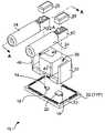
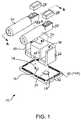
- FIG. 1is an exploded view illustrating the primary components of an optical sub-assembly having a packaging scheme in accordance with the present invention
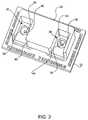
- FIG. 2is a detailed isometric view of the standoff and substrate of the optical sub-assembly of FIG. 1 ;
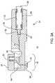
- FIGS. 3A and 3Brespectively show detailed elevation and isometric views of the polymer optical module used in the optical sub-assembly
- FIG. 4is a cross-sectional view of a polymer optical module, standoff, and substrate taken along section cut AA in FIG. 1 ;
- FIG. 5is a flowchart illustrating the alignment process used during assembly of the optical sub-assembly.
- FIG. 6is an isometric view of the optical sub-assembly that is used for illustrating an alignment of a polymer optical module.
- the present inventionprovides an optical sub-assembly that may be used in high-bandwidth transceivers having a packaging scheme that ensures that alignment between signal sending and detecting components is optimized and maintained over the lifetime of the device.
- the packaging schemeincludes a pair of polymer optical modules, which are used to couple light transmitted to and received from respective fiber optic cables. During a pre-alignment process, head portions of the polymer optical modules are inserted into respective slots defined in a standoff that is mounted on an optical sub-assembly substrate to which an emitter and detector are mounted. During a subsequent active alignment process, each polymer optical module is positioned relative to its respective emitter or detector until a maximum signal is detected, whereupon the position of the components is quick-set using a UV-sensitive adhesive. Optionally, additional adhesive may be used to further secure the components.
- the resulting packaging schemeprovides a single unit that supports both transmitter and receiver connection functions, while supporting bandwidths corresponding to 10 gigabit/second signals.
- FIG. 1An exploded view illustrating the primary components of an optical sub assembly (OSA) 10 that implements the packing scheme of the invention is shown in FIG. 1 .
- These componentsinclude an optical sub assembly (OSA) substrate 12 on which a vertical cavity surface emitting laser (VCSEL) 14 , a power monitor 16 , a detector 18 , and an amplifier 20 are mounted.
- the optical sub assemblyalso includes a standoff 22 , a pair of polymer optical modules 24 , and a pair of caps 28 .
- VCSEL 14is used to generate light signals that are used for high-bandwidth communication (e.g., 10 GHz/sec).
- the wavelength of the lightis approximately 800–900 nanometers(nm) (nominally 850 nm).
- VCSEL 14is configured to produce light with wavelengths of approximately 1300 nm and 1550 nm, respectively.
- other wavelengths suitable for high-bandwidth communication signal environmentsmay also be used.
- Suitable components that may be used for VCSEL 14include an Emcore (Albuquerque, N.Mex.) 8585–8050 GaAs VCSEL, or a GaAs VCSEL with similar characteristics manufactured by the Honeywell Corporation.
- the optical power emitted by VCSEL 14is monitored by power monitor 16 , which preferably comprises a low frequency power monitor photodiode that provides active control of the power emitted from VCSEL 14 .
- a portion of the optical power emitted from VCSEL 14is reflected from a lens 56 disposed above the VCSEL such that the reflected light is incident upon the aperture of power monitor 16 , wherein the incident light is calibrated to represent the actual optical power output by VCSEL 14 .
- Detector 18is used to detect high bandwidth (e.g., 10 GHz/sec) light signals having characteristics that are similar to the light signals produced by VCSEL 14 .
- Suitable components for detector 18include various GaAs detectors manufactured by the Microsemi Corporation of Santa Ana, Calif.
- Amplifier 20receives low current signals from detector 18 and provides gain to the signal while also injecting as little noise as possible into the data stream. This component generally will comprise a trans-impedance (TIA)-type amplifier, or a pre-amplifier. Nortel manufactures SiGe TIA amplifiers that may be implemented to perform the functions of amplifier 20 .
- TIAtrans-impedance
- power monitor 16is wire-bonded to OSA substrate 12 , which preferably comprises silicon, ceramic, or FR4.
- Amplifier 20may also be wire-bonded to OSA substrate 12 , or it may be electrically coupled to the OSA substrate using other techniques commonly used during electronic manufacturing, such as wave soldering. These components receive power and electrical signals via internal or surface traces in OSA substrate 12 (not shown), which are routed to a plurality of C4 solder bumps 32 disposed about the periphery of the OSA substrate.
- Standoff 22includes a pair of substantially cube-shaped recesses 38 and 40 configured to receive a block-shaped head portion 42 of polymer optical module 24 , whereby the head portions and sidewalls of the recesses slidedly engage (i.e., slide against one another) upon assembly, further details of which are described below.
- a pair of chamfers 44 and 46are also defined in the openings of recesses 38 and 40 , as well as a pair of countersunk holes 34 and 36 .
- standoff 22preferably should include EMI shielding to reduce and/or prevent cross-talk between received and transmitted signals. Accordingly, in one embodiment, gold or another suitable metal is deposited one the surfaces of recesses 38 and 40 , using, e.g., vapor deposition. In another embodiment, metal shielding is molded into the sidewall of recesses 38 and 40 .
- polymer optical module 24is used to redirect light being produced by VCSEL 14 so that it may be received by a fiber optic cable, and redirect light received from a fiber optic cable so that it may be received at detector 18 .
- polymer optical module 24is made of a material that enables passage of light having a wavelength corresponding to the light signals used for the high-bandwidth environments the apparatus is to be used in.
- the wavelength of the lightis approximately 800–900 nm.
- 1300 nm and 1550 nm light signalsmay also be used, as well as other wavelengths.
- Polymer optical module 24also includes a cylindrical bore 50 defined in one end that is configured to receive an end portion 52 of a fiber optic cable 54 , as shown in FIGS.
- Bore 50also includes a stepped down portion 55 for receiving a fiber end or area 57 of fiber optic cable 54 .
- Materials suitable for polymer optical module 24include Ultem 1000, a polymer manufactured by General Electric, which has a coefficient of refraction of approximately 3.
- Polymer optical module 24includes a pair of lenses 56 and 58 that are used to collimate incoming and outgoing light signals, as depicted by a light pathway 60 .
- lenses 56 and 58are formed directly into polymer optical module 24 .
- lenses 56 and/or 58may comprise separate components that are mounted within the module.
- Polymer optical module 24preferably has a cylindrical shape over most of its length with a chamfer 66 defined toward the head end that mates with chamfer 44 or 46 .
- Polymer optical module 24also includes a recess 64 , which is preferably filled with air. As light travels along light pathway 60 , it impinges upon a surface 62 defined in recess 64 , whereupon the light is redirected approximately 90 degrees. This “mirroring” effect is produced by the different coefficients of refraction on the two sides of surface 62 (3 for Ultem 1000, 1 for air). Cap 28 is used to ensure that the air in recess 64 remains free of dust and other impurities
- VCSEL 14 and detector 18In order to maximize performance, the alignment of VCSEL 14 and detector 18 relative to lenses 56 in polymer optical modules 24 need to be precisely controlled. Accurate alignment of these components is enabled through a two-phase pre-alignment and active alignment process.
- the pre-alignment phaseensures that minimal positional adjustment needs to be performed during the active-alignment phase. This is a result of minimizing the tolerance stack up of the assembly.
- VCSEL 14 and detector 18are positioned relative to a known datum or registration point on OSA substrate 12 so as to have a position error of approximately +/ ⁇ 20 ⁇ m.
- countersunk holes 34 and 36are positioned relative to a known datum or reference point on OSA substrate 12 to have a position error of +/ ⁇ 20 ⁇ m upon assembly.
- the OSA substrate and standoffpreferably are assembled using an epoxy or a similar adhesive.
- the depth of recesses 38 and 40are precisely Controlled such that the focal point of lens 56 falls upon emitter 14 or detector 18 , as
- standoff 22 and polymer optical modules 24In order to obtain the foregoing alignment results, various surfaces and features on standoff 22 and polymer optical modules 24 must be very accurate. Accordingly, standoff 22 and polymer optical modules 24 will require a precision manufacturing process, such as precision injection molding. In alternate embodiments, these precision surfaces and features may be obtained using post-molding machining operations.
- the pre-alignment phasebegins in a block 100 in which an adhesive 70 is applied to the sides of head 42 and/or the sides and/or bottom of recess 40 .
- adhesive 70may be inserted into the gap between the sides of head 42 and recess 40 , as shown in FIG. 6 , after the step performed in block 102 discussed below.
- adhesive 70will comprise a cyanoacrylate or epoxy that is sensitive to ultra-violet (UV) light, such that the adhesive rapidly cures when exposed to UV light.
- UVultra-violet
- adhesive 70may comprise two or more adhesives, wherein one of the adhesives is sensitive to UV light, while the other adhesive(s) provides additional rigidity to the assembly upon being cured, such as various well-known high-strength epoxies.
- a head portion 42 of a polymer optical module 24is inserted into a recess 38 (or 40 ) and frustro-conical boss 59 is inserted into countersunk hole 36 (or 34 ).
- the size and configuration of the various features on the mating partsis such that there is a slight gap defined between the sides of head 42 and respective sides of the recess, and there is approximately 100 ⁇ m of play between the angled surfaces of the countersink and cone of frustro-conical boss 59 .
- the pre-alignment phase of the alignment processis complete.
- the next part of the alignment processcomprises an active alignment of each polymer optical module 24 relative to standoff 22 (and thus VCSEL 14 and detector 18 ). As provided by a block 104 , this is accomplished by adjusting the position of each polymer optical module 24 while measuring either an output signal strength of the light produced by VCSEL 14 or the strength of an input signal as measured by detector 18 (as appropriate for that polymer optical module), wherein positioning continues until a maximum signal is detected.
- the signal strength measurementis depicted as blocks 72 and 74 in FIG. 6 .
- UV lightis applied to adhesive 70 in a block 106 to quick-set the position. If it hasn't been previously added above, additional adhesive, such as a high-strength epoxy, may then be applied in the gap between the sides of head 42 and recess 36 to secure the position, as provided by a block 108 .
- additional adhesivesuch as a high-strength epoxy
- a similar alignment processis then performed on the polymer optical module for the other side.
- active alignment of both polymer optical modules 24may be performed substantially simultaneously.
- the resulting assemblycomprises a monolithic high-density SFF (Small Form Factor) connector suitable for use in Gigabit transceivers, allowing for horizontal fiber coupling. Due to the active alignment process, the signal strength of the transceiver is maximized.
- SFFSmall Form Factor
Landscapes
- Physics & Mathematics (AREA)
- General Physics & Mathematics (AREA)
- Optics & Photonics (AREA)
- Electromagnetism (AREA)
- Optical Couplings Of Light Guides (AREA)
Abstract
Description
The present application is a continuation of application Ser. No. 09/823,294, filed Mar. 29, 2001, now U.S. Pat. No. 6,692,161, the benefit of the priority date of which is claimed under 35 U.S.C. § 120.
1. Field of the Invention
The present invention generally concerns very high bandwidth transceivers, and in more particular concerns a packaging scheme for very high bandwidth transceivers in which an emitter and detector are packaged in a monolithic unit.
2. Background Information
Network communications have dramatically increased access to data, enabling larger and larger volumes of data to be transmitted. In order to facilitate the ever-increasing request for data transfers, communications systems have progressively increased their bandwidth. For example, the developers of Ethernet network technology provide standards for transfer rates of 10 megabits/second, 100 megabits/second, and 1 gigabit/second. Recently, standards are being formulated for 10 gigabit/second Ethernet networks.
Network communications involve a transfer of data between two endpoint devices (e.g., computers) that are generally coupled by one or more intermediate devices. For example, when accessing data via the Internet, the intermediate devices for the datapath (i.e., the network routing over which the data is transmitted) may comprise one or more gateways and various routers and switches. When using a local area network (LAN), the datapath typically comprises one or more hubs and/or routers. Each device in the datapath must provide appropriate connections that enable signals provided via network cabling to be received and transmitted by those devices.
To support the higher bandwidth signals, gigabit/second networks generally require optical fiber cabling, which provides several advantages over copper cabling. A fiber optic connection provides two functions: it couples a transmitter light signal produced by an emitter to the fiber optic cabling, and it provides a means for coupling a received light signal on the fiber optic cable to a receiving component, typically comprising a detector. As the bandwidth of network signals increase, their signal-to-noise ratio decreases, making the higher bandwidth signals, even when carried over fiber optic cabling, more sensitive to disturbances such as EMI radiation and the like. This requires the alignment of the components in a connector to be very precise. Additionally, increased measures must be taken to prevent external disturbances.
One conventional packaging scheme that is designed for high-bandwidth applications is known in the industry as a “TO can” package. Connectors that employ TO can packages include separate packages for coupling the transmitted signal and the received signal. The outputs of these packages are generally coupled to a circuit board that enables further routing and/or processing of the transmitted or received signals. At present, TO can packages generally support bandwidths of approximately 2.5 Gigabits/second.
The foregoing aspects and many of the attendant advantages of this invention will become more readily appreciated as the same becomes better understood by reference to the following detailed description, when taken in conjunction with the accompanying drawings, wherein:
The present invention provides an optical sub-assembly that may be used in high-bandwidth transceivers having a packaging scheme that ensures that alignment between signal sending and detecting components is optimized and maintained over the lifetime of the device. The packaging scheme includes a pair of polymer optical modules, which are used to couple light transmitted to and received from respective fiber optic cables. During a pre-alignment process, head portions of the polymer optical modules are inserted into respective slots defined in a standoff that is mounted on an optical sub-assembly substrate to which an emitter and detector are mounted. During a subsequent active alignment process, each polymer optical module is positioned relative to its respective emitter or detector until a maximum signal is detected, whereupon the position of the components is quick-set using a UV-sensitive adhesive. Optionally, additional adhesive may be used to further secure the components. The resulting packaging scheme provides a single unit that supports both transmitter and receiver connection functions, while supporting bandwidths corresponding to 10 gigabit/second signals.
An exploded view illustrating the primary components of an optical sub assembly (OSA)10 that implements the packing scheme of the invention is shown inFIG. 1 . These components include an optical sub assembly (OSA)substrate 12 on which a vertical cavity surface emitting laser (VCSEL)14, apower monitor 16, adetector 18, and anamplifier 20 are mounted. The optical sub assembly also includes astandoff 22, a pair of polymeroptical modules 24, and a pair ofcaps 28.
VCSEL14 is used to generate light signals that are used for high-bandwidth communication (e.g., 10 GHz/sec). In one embodiment, the wavelength of the light is approximately 800–900 nanometers(nm) (nominally 850 nm). In other embodiments, VCSEL14 is configured to produce light with wavelengths of approximately 1300 nm and 1550 nm, respectively. In addition, other wavelengths suitable for high-bandwidth communication signal environments may also be used. Suitable components that may be used for VCSEL14 include an Emcore (Albuquerque, N.Mex.) 8585–8050 GaAs VCSEL, or a GaAs VCSEL with similar characteristics manufactured by the Honeywell Corporation. The optical power emitted by VCSEL14 is monitored bypower monitor 16, which preferably comprises a low frequency power monitor photodiode that provides active control of the power emitted from VCSEL14. A portion of the optical power emitted from VCSEL14 is reflected from alens 56 disposed above the VCSEL such that the reflected light is incident upon the aperture ofpower monitor 16, wherein the incident light is calibrated to represent the actual optical power output by VCSEL14.
Preferably,power monitor 16 is wire-bonded toOSA substrate 12, which preferably comprises silicon, ceramic, or FR4.Amplifier 20 may also be wire-bonded toOSA substrate 12, or it may be electrically coupled to the OSA substrate using other techniques commonly used during electronic manufacturing, such as wave soldering. These components receive power and electrical signals via internal or surface traces in OSA substrate12 (not shown), which are routed to a plurality ofC4 solder bumps 32 disposed about the periphery of the OSA substrate.
A detailed view ofOSA substrate 12 andstandoff 22 upon assembly is shown inFIG. 2 .Standoff 22 includes a pair of substantially cube-shaped recesses shaped head portion 42 of polymeroptical module 24, whereby the head portions and sidewalls of the recesses slidedly engage (i.e., slide against one another) upon assembly, further details of which are described below. A pair ofchamfers recesses countersunk holes standoff 22 preferably should include EMI shielding to reduce and/or prevent cross-talk between received and transmitted signals. Accordingly, in one embodiment, gold or another suitable metal is deposited one the surfaces ofrecesses recesses
The polymer optical modules are used to redirect light being produced byVCSEL 14 so that it may be received by a fiber optic cable, and redirect light received from a fiber optic cable so that it may be received atdetector 18. Accordingly, polymeroptical module 24 is made of a material that enables passage of light having a wavelength corresponding to the light signals used for the high-bandwidth environments the apparatus is to be used in. For example, in one embodiment the wavelength of the light is approximately 800–900 nm. As discussed above, 1300 nm and 1550 nm light signals may also be used, as well as other wavelengths. Polymeroptical module 24 also includes acylindrical bore 50 defined in one end that is configured to receive anend portion 52 of afiber optic cable 54, as shown inFIGS. 3A ,3B and4.Bore 50 also includes a stepped downportion 55 for receiving a fiber end orarea 57 offiber optic cable 54. Materials suitable for polymeroptical module 24 include Ultem 1000, a polymer manufactured by General Electric, which has a coefficient of refraction of approximately 3.
Polymeroptical module 24 includes a pair oflenses light pathway 60. Preferably,lenses optical module 24. Optionally,lenses 56 and/or58 may comprise separate components that are mounted within the module. Polymeroptical module 24 preferably has a cylindrical shape over most of its length with achamfer 66 defined toward the head end that mates withchamfer
Polymeroptical module 24 also includes arecess 64, which is preferably filled with air. As light travels alonglight pathway 60, it impinges upon asurface 62 defined inrecess 64, whereupon the light is redirected approximately 90 degrees. This “mirroring” effect is produced by the different coefficients of refraction on the two sides of surface62 (3 for Ultem 1000, 1 for air).Cap 28 is used to ensure that the air inrecess 64 remains free of dust and other impurities
In order to maximize performance, the alignment ofVCSEL 14 anddetector 18 relative tolenses 56 in polymeroptical modules 24 need to be precisely controlled. Accurate alignment of these components is enabled through a two-phase pre-alignment and active alignment process. The pre-alignment phase ensures that minimal positional adjustment needs to be performed during the active-alignment phase. This is a result of minimizing the tolerance stack up of the assembly. Accordingly,VCSEL 14 anddetector 18 are positioned relative to a known datum or registration point onOSA substrate 12 so as to have a position error of approximately +/−20 μm. Furthermore, countersunkholes OSA substrate 12 to have a position error of +/−20 μm upon assembly. The OSA substrate and standoff preferably are assembled using an epoxy or a similar adhesive. Finally, the depth ofrecesses lens 56 falls uponemitter 14 ordetector 18, as appropriate.
In order to obtain the foregoing alignment results, various surfaces and features onstandoff 22 and polymeroptical modules 24 must be very accurate. Accordingly,standoff 22 and polymeroptical modules 24 will require a precision manufacturing process, such as precision injection molding. In alternate embodiments, these precision surfaces and features may be obtained using post-molding machining operations.
With reference to the flowchart ofFIG. 5 , the pre-alignment phase begins in ablock 100 in which an adhesive70 is applied to the sides ofhead 42 and/or the sides and/or bottom ofrecess 40. Optionally, adhesive70 may be inserted into the gap between the sides ofhead 42 andrecess 40, as shown inFIG. 6 , after the step performed inblock 102 discussed below. Preferably, adhesive70 will comprise a cyanoacrylate or epoxy that is sensitive to ultra-violet (UV) light, such that the adhesive rapidly cures when exposed to UV light. Optionally, adhesive70 may comprise two or more adhesives, wherein one of the adhesives is sensitive to UV light, while the other adhesive(s) provides additional rigidity to the assembly upon being cured, such as various well-known high-strength epoxies.
Next, in ablock 102, ahead portion 42 of a polymeroptical module 24 is inserted into a recess38 (or40) and frustro-conical boss 59 is inserted into countersunk hole36 (or34). The size and configuration of the various features on the mating parts is such that there is a slight gap defined between the sides ofhead 42 and respective sides of the recess, and there is approximately 100 μm of play between the angled surfaces of the countersink and cone of frustro-conical boss 59. At this point, the pre-alignment phase of the alignment process is complete.
The next part of the alignment process comprises an active alignment of each polymeroptical module 24 relative to standoff22 (and thusVCSEL 14 and detector18). As provided by ablock 104, this is accomplished by adjusting the position of each polymeroptical module 24 while measuring either an output signal strength of the light produced byVCSEL 14 or the strength of an input signal as measured by detector18 (as appropriate for that polymer optical module), wherein positioning continues until a maximum signal is detected. The signal strength measurement is depicted asblocks FIG. 6 .
Upon detection of a maximum signal, UV light is applied to adhesive70 in ablock 106 to quick-set the position. If it hasn't been previously added above, additional adhesive, such as a high-strength epoxy, may then be applied in the gap between the sides ofhead 42 andrecess 36 to secure the position, as provided by ablock 108.
A similar alignment process is then performed on the polymer optical module for the other side. Optionally, active alignment of both polymeroptical modules 24 may be performed substantially simultaneously.
After the adhesive(s) have cured, the resulting assembly comprises a monolithic high-density SFF (Small Form Factor) connector suitable for use in Gigabit transceivers, allowing for horizontal fiber coupling. Due to the active alignment process, the signal strength of the transceiver is maximized.
The above description of illustrated embodiments of the invention is not intended to be exhaustive or to limit the invention to the precise forms disclosed. While specific embodiments of, and examples for, the invention are described herein for illustrative purposes, various equivalent modifications are possible within the scope of the invention, as those skilled in the relevant art will recognize. Accordingly, it is not intended that the scope of the invention in any way be limited by the above description, but instead be determined entirely by reference to the claims that follow.
Claims (23)
1. An apparatus comprising:
a substrate on which a light emitter and a light detector are mounted;
a first optical module adapted to optically couple light received from a first optical cable to the light detector, said first optical module including a first lens to collimate light received from the first optical cable and a second lens optically coupled to the first lens to focus received collimated light onto the light detector, said first optical module including a head portion;
a second optical module adapted to optically couple light produced by the light emitter to a second optical cable, said second optical module including a first lens to collimate light received from the light emitter and a second lens optically coupled to the first lens to direct light into the second optical cable, said second optical module including a head portion;
wherein each of the first and second optical modules comprise a single piece polymer structure;
a standoff fixedly mounted to the substrate, said standoff including two recesses defined therein, each said recess to engage the head portion of a respective optical module wherein at least one gap is formed between the head portion of each optical module and the respective recess, said gap to allow active alignment of an optical module wherein the optical module is positioned within the respective recess such that a maximum amount of light is optically coupled; and
epoxy disposed in said gap for fixedly securing the head portion of an optical module to a respective recess upon completion of said active alignment.
2. The apparatus ofclaim 1 , wherein the recesses are adapted to slidedly engage a head portion of a respective optical module during an assembly operation, each of said head portions being fixedly secured within a respective recess upon completion of the assembly operation.
3. The apparatus ofclaim 2 , wherein each of the first and second optical modules includes a boss extending outward from the head portion of that optical module and wherein a respective hole is defined in a base portion of each of the recesses that is adapted to substantially mate with a respective boss during the assembly operation.
4. The apparatus ofclaim 3 , wherein the boss comprises a frustro-conical shape defining a cone angle, and each hole includes a countersink having an angle substantially matching the cone angle.
5. The apparatus ofclaim 1 , wherein each of the first and second optical modules include a bore adapted to couple to an end portion of the first and second optical cables, respectively.
6. The apparatus ofclaim 1 , wherein the first and second lenses of each of the first and second optical modules are disposed approximately 90 degrees from one another, and each optical module further includes a recess filled with a material having a coefficient of refraction different than a coefficient of refraction of a material from which the optical modules are made and defining a reflection surface such that light received by one of the first and second lenses is redirected toward the other lens.
7. The apparatus ofclaim 6 , wherein each of the first and second optical modules further includes a respective cap that covers the recess to prevent impurities from entering the recess.
8. The apparatus ofclaim 1 , wherein the light emitter comprises a vertical cavity surface emitting laser (VCSEL).
9. The apparatus ofclaim 1 , wherein the first optical module is positioned relative to the light detector such that a maximum amount of light received from the first optical cable is directed toward the light detector.
10. The apparatus ofclaim 9 , wherein the first optical module is positioned relative to the light detector using an active alignment process wherein an alignment between the first optical module and the light detector is adjusted until a maximum signal is detected at the light detector, whereupon the alignment is fixedly secured.
11. The apparatus ofclaim 1 , wherein the second optical module is positioned relative to the light emitter such that a maximum amount of light produced by the light emitter is received by the second optical cable.
12. The apparatus ofclaim 11 , wherein the second optical module is positioned relative to the light emitter using an active alignment process wherein an alignment between the second optical module and the light emitter is adjusted until a maximum signal is detected at the second optical cable, whereupon the alignment is fixedly secured.
13. The apparatus ofclaim 1 , wherein the substrate further includes a plurality of solder bumps to connect to an external component, a portion of which are electrically coupled to the light emitter and light detector.
14. The apparatus ofclaim 1 , wherein the standoff further includes shielding disposed along sidewalls of its two recesses to prevent cross-talk between light signals passing through the head portions of the first and second optical modules.
15. The apparatus ofclaim 1 , further including an amplifier mounted to the substrate that receives a light detection signal output by the light detector, and a power monitor mounted to the substrate that actively controls a power level supplied to the light emitter.
16. The apparatus ofclaim 1 , wherein said epoxy is an ultra-violet (“UV”) sensitive adhesive, wherein said UV-sensitive adhesive cures when exposed to ultra-violet light.
17. An apparatus comprising:
a first light coupling means for optically coupling light received from a first optical cable to a light detector having an optical axis oriented approximately 90 degrees relative to an optical axis of the first optical cable, said first light coupling means including a head portion;
a second light coupling means for optically coupling light produced by a light emitter to a second optical cable having an optical axis that is approximately 90 degrees relative to an optical axis of the light emitter, said second light coupling means including a head portion;
wherein each of the first and second light coupling means comprice a single piece polymer structure;
a substrate on which the light emitter and the light detector are mounted;
means for fixedly coupling the first and second light coupling means to the substrate, wherein said means for fixedly coupling the first and second light coupling means includes a pair of recesses to engage the head portions of each respective light coupling means, wherein at least one gap is formed between the head portion of each light coupling means and the respective recess, said gap to allow active alignment of a light coupling means wherein the light coupling means is positioned within the respective recess such that a maximum amount of light is coupled; and
epoxy disposed in said gap for fixedly securing the head portion of a light coupling means to a respective recess upon completion of said active alignment.
18. The apparatus ofclaim 17 , wherein the means for fixedly coupling the first and second light coupling means includes means to substantially align optical features in the first light coupling means to the light detector and substantially align optical features in the second light coupling means to the light emitter.
19. The apparatus ofclaim 17 , wherein the recesses are adapted to slidedly engage the head portions of respective light coupling means.
20. The apparatus ofclaim 17 , wherein each of the first and second light coupling means includes means for coupling to a fiber optic cable.
21. The apparatus ofclaim 17 , wherein the second optical coupling means is positioned relative to the light emitter such that a maximum amount of light produced by the light emitter is received by the second optical cable.
22. The apparatus ofclaim 17 , wherein the second optical coupling means is positioned relative to the light emitter such that a maximum amount of light produced by the light emitter is received by the second optical cable.
23. The apparatus ofclaim 17 , wherein said epoxy is an ultra-violet (“UV”) sensitive adhesive, wherein said UV-sensitive adhesive cures when exposed to ultra-violet light.
Priority Applications (1)
| Application Number | Priority Date | Filing Date | Title |
|---|---|---|---|
| US10/638,005US7008120B2 (en) | 2001-03-29 | 2003-08-08 | High frequency emmitter and detector packaging scheme for 10GB/S transceiver |
Applications Claiming Priority (2)
| Application Number | Priority Date | Filing Date | Title |
|---|---|---|---|
| US09/823,294US6692161B2 (en) | 2001-03-29 | 2001-03-29 | High frequency emitter and detector packaging scheme for 10GB/S transceiver |
| US10/638,005US7008120B2 (en) | 2001-03-29 | 2003-08-08 | High frequency emmitter and detector packaging scheme for 10GB/S transceiver |
Related Parent Applications (1)
| Application Number | Title | Priority Date | Filing Date |
|---|---|---|---|
| US09/823,294ContinuationUS6692161B2 (en) | 2001-03-29 | 2001-03-29 | High frequency emitter and detector packaging scheme for 10GB/S transceiver |
Publications (2)
| Publication Number | Publication Date |
|---|---|
| US20040033031A1 US20040033031A1 (en) | 2004-02-19 |
| US7008120B2true US7008120B2 (en) | 2006-03-07 |
Family
ID=25238341
Family Applications (2)
| Application Number | Title | Priority Date | Filing Date |
|---|---|---|---|
| US09/823,294Expired - LifetimeUS6692161B2 (en) | 2001-03-29 | 2001-03-29 | High frequency emitter and detector packaging scheme for 10GB/S transceiver |
| US10/638,005Expired - Fee RelatedUS7008120B2 (en) | 2001-03-29 | 2003-08-08 | High frequency emmitter and detector packaging scheme for 10GB/S transceiver |
Family Applications Before (1)
| Application Number | Title | Priority Date | Filing Date |
|---|---|---|---|
| US09/823,294Expired - LifetimeUS6692161B2 (en) | 2001-03-29 | 2001-03-29 | High frequency emitter and detector packaging scheme for 10GB/S transceiver |
Country Status (5)
| Country | Link |
|---|---|
| US (2) | US6692161B2 (en) |
| CN (1) | CN1272646C (en) |
| AU (1) | AU2002252231A1 (en) |
| TW (1) | TW554619B (en) |
| WO (1) | WO2002079824A2 (en) |
Cited By (165)
| Publication number | Priority date | Publication date | Assignee | Title |
|---|---|---|---|---|
| US9119127B1 (en) | 2012-12-05 | 2015-08-25 | At&T Intellectual Property I, Lp | Backhaul link for distributed antenna system |
| US20150247984A1 (en)* | 2014-02-28 | 2015-09-03 | Murata Manufacturing Co., Ltd. | Optical transmission module and method of manufacturing optical transmission module |
| US9154966B2 (en) | 2013-11-06 | 2015-10-06 | At&T Intellectual Property I, Lp | Surface-wave communications and methods thereof |
| US20150331212A1 (en)* | 2013-01-31 | 2015-11-19 | Ccs Technology, Inc. | Method for forming optoelectronic modules connectable to optical fibers and optoelectronic module connectable to at least one optical fiber |
| US9209902B2 (en) | 2013-12-10 | 2015-12-08 | At&T Intellectual Property I, L.P. | Quasi-optical coupler |
| US9312919B1 (en) | 2014-10-21 | 2016-04-12 | At&T Intellectual Property I, Lp | Transmission device with impairment compensation and methods for use therewith |
| US9461706B1 (en) | 2015-07-31 | 2016-10-04 | At&T Intellectual Property I, Lp | Method and apparatus for exchanging communication signals |
| US9490869B1 (en) | 2015-05-14 | 2016-11-08 | At&T Intellectual Property I, L.P. | Transmission medium having multiple cores and methods for use therewith |
| US9503189B2 (en) | 2014-10-10 | 2016-11-22 | At&T Intellectual Property I, L.P. | Method and apparatus for arranging communication sessions in a communication system |
| US9509415B1 (en) | 2015-06-25 | 2016-11-29 | At&T Intellectual Property I, L.P. | Methods and apparatus for inducing a fundamental wave mode on a transmission medium |
| US9520945B2 (en) | 2014-10-21 | 2016-12-13 | At&T Intellectual Property I, L.P. | Apparatus for providing communication services and methods thereof |
| US9525210B2 (en) | 2014-10-21 | 2016-12-20 | At&T Intellectual Property I, L.P. | Guided-wave transmission device with non-fundamental mode propagation and methods for use therewith |
| US9525524B2 (en) | 2013-05-31 | 2016-12-20 | At&T Intellectual Property I, L.P. | Remote distributed antenna system |
| US9531427B2 (en) | 2014-11-20 | 2016-12-27 | At&T Intellectual Property I, L.P. | Transmission device with mode division multiplexing and methods for use therewith |
| US9564947B2 (en) | 2014-10-21 | 2017-02-07 | At&T Intellectual Property I, L.P. | Guided-wave transmission device with diversity and methods for use therewith |
| US9577307B2 (en) | 2014-10-21 | 2017-02-21 | At&T Intellectual Property I, L.P. | Guided-wave transmission device and methods for use therewith |
| US9608740B2 (en) | 2015-07-15 | 2017-03-28 | At&T Intellectual Property I, L.P. | Method and apparatus for launching a wave mode that mitigates interference |
| US9608692B2 (en) | 2015-06-11 | 2017-03-28 | At&T Intellectual Property I, L.P. | Repeater and methods for use therewith |
| US9615269B2 (en) | 2014-10-02 | 2017-04-04 | At&T Intellectual Property I, L.P. | Method and apparatus that provides fault tolerance in a communication network |
| US9628854B2 (en) | 2014-09-29 | 2017-04-18 | At&T Intellectual Property I, L.P. | Method and apparatus for distributing content in a communication network |
| US9628116B2 (en) | 2015-07-14 | 2017-04-18 | At&T Intellectual Property I, L.P. | Apparatus and methods for transmitting wireless signals |
| US9640850B2 (en) | 2015-06-25 | 2017-05-02 | At&T Intellectual Property I, L.P. | Methods and apparatus for inducing a non-fundamental wave mode on a transmission medium |
| US9654173B2 (en) | 2014-11-20 | 2017-05-16 | At&T Intellectual Property I, L.P. | Apparatus for powering a communication device and methods thereof |
| US9653770B2 (en) | 2014-10-21 | 2017-05-16 | At&T Intellectual Property I, L.P. | Guided wave coupler, coupling module and methods for use therewith |
| US9667317B2 (en) | 2015-06-15 | 2017-05-30 | At&T Intellectual Property I, L.P. | Method and apparatus for providing security using network traffic adjustments |
| US9680670B2 (en) | 2014-11-20 | 2017-06-13 | At&T Intellectual Property I, L.P. | Transmission device with channel equalization and control and methods for use therewith |
| US9685992B2 (en) | 2014-10-03 | 2017-06-20 | At&T Intellectual Property I, L.P. | Circuit panel network and methods thereof |
| US9692101B2 (en) | 2014-08-26 | 2017-06-27 | At&T Intellectual Property I, L.P. | Guided wave couplers for coupling electromagnetic waves between a waveguide surface and a surface of a wire |
| US9705571B2 (en) | 2015-09-16 | 2017-07-11 | At&T Intellectual Property I, L.P. | Method and apparatus for use with a radio distributed antenna system |
| US9705561B2 (en) | 2015-04-24 | 2017-07-11 | At&T Intellectual Property I, L.P. | Directional coupling device and methods for use therewith |
| US9722318B2 (en) | 2015-07-14 | 2017-08-01 | At&T Intellectual Property I, L.P. | Method and apparatus for coupling an antenna to a device |
| US9729197B2 (en) | 2015-10-01 | 2017-08-08 | At&T Intellectual Property I, L.P. | Method and apparatus for communicating network management traffic over a network |
| US9735833B2 (en) | 2015-07-31 | 2017-08-15 | At&T Intellectual Property I, L.P. | Method and apparatus for communications management in a neighborhood network |
| US9742462B2 (en) | 2014-12-04 | 2017-08-22 | At&T Intellectual Property I, L.P. | Transmission medium and communication interfaces and methods for use therewith |
| US9748626B2 (en) | 2015-05-14 | 2017-08-29 | At&T Intellectual Property I, L.P. | Plurality of cables having different cross-sectional shapes which are bundled together to form a transmission medium |
| US9749053B2 (en) | 2015-07-23 | 2017-08-29 | At&T Intellectual Property I, L.P. | Node device, repeater and methods for use therewith |
| US9749013B2 (en) | 2015-03-17 | 2017-08-29 | At&T Intellectual Property I, L.P. | Method and apparatus for reducing attenuation of electromagnetic waves guided by a transmission medium |
| US9755697B2 (en) | 2014-09-15 | 2017-09-05 | At&T Intellectual Property I, L.P. | Method and apparatus for sensing a condition in a transmission medium of electromagnetic waves |
| US9762289B2 (en) | 2014-10-14 | 2017-09-12 | At&T Intellectual Property I, L.P. | Method and apparatus for transmitting or receiving signals in a transportation system |
| US9769128B2 (en) | 2015-09-28 | 2017-09-19 | At&T Intellectual Property I, L.P. | Method and apparatus for encryption of communications over a network |
| US9769020B2 (en) | 2014-10-21 | 2017-09-19 | At&T Intellectual Property I, L.P. | Method and apparatus for responding to events affecting communications in a communication network |
| US9780834B2 (en) | 2014-10-21 | 2017-10-03 | At&T Intellectual Property I, L.P. | Method and apparatus for transmitting electromagnetic waves |
| US9793954B2 (en) | 2015-04-28 | 2017-10-17 | At&T Intellectual Property I, L.P. | Magnetic coupling device and methods for use therewith |
| US9793951B2 (en) | 2015-07-15 | 2017-10-17 | At&T Intellectual Property I, L.P. | Method and apparatus for launching a wave mode that mitigates interference |
| US9793955B2 (en) | 2015-04-24 | 2017-10-17 | At&T Intellectual Property I, Lp | Passive electrical coupling device and methods for use therewith |
| US9800327B2 (en) | 2014-11-20 | 2017-10-24 | At&T Intellectual Property I, L.P. | Apparatus for controlling operations of a communication device and methods thereof |
| US9820146B2 (en) | 2015-06-12 | 2017-11-14 | At&T Intellectual Property I, L.P. | Method and apparatus for authentication and identity management of communicating devices |
| US9838896B1 (en) | 2016-12-09 | 2017-12-05 | At&T Intellectual Property I, L.P. | Method and apparatus for assessing network coverage |
| US9836957B2 (en) | 2015-07-14 | 2017-12-05 | At&T Intellectual Property I, L.P. | Method and apparatus for communicating with premises equipment |
| US9847566B2 (en) | 2015-07-14 | 2017-12-19 | At&T Intellectual Property I, L.P. | Method and apparatus for adjusting a field of a signal to mitigate interference |
| US9847850B2 (en) | 2014-10-14 | 2017-12-19 | At&T Intellectual Property I, L.P. | Method and apparatus for adjusting a mode of communication in a communication network |
| US9853342B2 (en) | 2015-07-14 | 2017-12-26 | At&T Intellectual Property I, L.P. | Dielectric transmission medium connector and methods for use therewith |
| US9860075B1 (en) | 2016-08-26 | 2018-01-02 | At&T Intellectual Property I, L.P. | Method and communication node for broadband distribution |
| US9865911B2 (en) | 2015-06-25 | 2018-01-09 | At&T Intellectual Property I, L.P. | Waveguide system for slot radiating first electromagnetic waves that are combined into a non-fundamental wave mode second electromagnetic wave on a transmission medium |
| US9866309B2 (en) | 2015-06-03 | 2018-01-09 | At&T Intellectual Property I, Lp | Host node device and methods for use therewith |
| US9871282B2 (en) | 2015-05-14 | 2018-01-16 | At&T Intellectual Property I, L.P. | At least one transmission medium having a dielectric surface that is covered at least in part by a second dielectric |
| US9871283B2 (en) | 2015-07-23 | 2018-01-16 | At&T Intellectual Property I, Lp | Transmission medium having a dielectric core comprised of plural members connected by a ball and socket configuration |
| US9876605B1 (en) | 2016-10-21 | 2018-01-23 | At&T Intellectual Property I, L.P. | Launcher and coupling system to support desired guided wave mode |
| US9876570B2 (en) | 2015-02-20 | 2018-01-23 | At&T Intellectual Property I, Lp | Guided-wave transmission device with non-fundamental mode propagation and methods for use therewith |
| US9876264B2 (en) | 2015-10-02 | 2018-01-23 | At&T Intellectual Property I, Lp | Communication system, guided wave switch and methods for use therewith |
| US9882277B2 (en) | 2015-10-02 | 2018-01-30 | At&T Intellectual Property I, Lp | Communication device and antenna assembly with actuated gimbal mount |
| US9882257B2 (en) | 2015-07-14 | 2018-01-30 | At&T Intellectual Property I, L.P. | Method and apparatus for launching a wave mode that mitigates interference |
| US9893795B1 (en) | 2016-12-07 | 2018-02-13 | At&T Intellectual Property I, Lp | Method and repeater for broadband distribution |
| US9906269B2 (en) | 2014-09-17 | 2018-02-27 | At&T Intellectual Property I, L.P. | Monitoring and mitigating conditions in a communication network |
| US9904535B2 (en) | 2015-09-14 | 2018-02-27 | At&T Intellectual Property I, L.P. | Method and apparatus for distributing software |
| US9912382B2 (en) | 2015-06-03 | 2018-03-06 | At&T Intellectual Property I, Lp | Network termination and methods for use therewith |
| US9911020B1 (en) | 2016-12-08 | 2018-03-06 | At&T Intellectual Property I, L.P. | Method and apparatus for tracking via a radio frequency identification device |
| US9912419B1 (en) | 2016-08-24 | 2018-03-06 | At&T Intellectual Property I, L.P. | Method and apparatus for managing a fault in a distributed antenna system |
| US9912027B2 (en) | 2015-07-23 | 2018-03-06 | At&T Intellectual Property I, L.P. | Method and apparatus for exchanging communication signals |
| US9913139B2 (en) | 2015-06-09 | 2018-03-06 | At&T Intellectual Property I, L.P. | Signal fingerprinting for authentication of communicating devices |
| US9917341B2 (en) | 2015-05-27 | 2018-03-13 | At&T Intellectual Property I, L.P. | Apparatus and method for launching electromagnetic waves and for modifying radial dimensions of the propagating electromagnetic waves |
| US9927517B1 (en) | 2016-12-06 | 2018-03-27 | At&T Intellectual Property I, L.P. | Apparatus and methods for sensing rainfall |
| US9948354B2 (en) | 2015-04-28 | 2018-04-17 | At&T Intellectual Property I, L.P. | Magnetic coupling device with reflective plate and methods for use therewith |
| US9948333B2 (en) | 2015-07-23 | 2018-04-17 | At&T Intellectual Property I, L.P. | Method and apparatus for wireless communications to mitigate interference |
| US9954287B2 (en) | 2014-11-20 | 2018-04-24 | At&T Intellectual Property I, L.P. | Apparatus for converting wireless signals and electromagnetic waves and methods thereof |
| US9967173B2 (en) | 2015-07-31 | 2018-05-08 | At&T Intellectual Property I, L.P. | Method and apparatus for authentication and identity management of communicating devices |
| US9973940B1 (en) | 2017-02-27 | 2018-05-15 | At&T Intellectual Property I, L.P. | Apparatus and methods for dynamic impedance matching of a guided wave launcher |
| US9991580B2 (en) | 2016-10-21 | 2018-06-05 | At&T Intellectual Property I, L.P. | Launcher and coupling system for guided wave mode cancellation |
| US9998870B1 (en) | 2016-12-08 | 2018-06-12 | At&T Intellectual Property I, L.P. | Method and apparatus for proximity sensing |
| US9997819B2 (en) | 2015-06-09 | 2018-06-12 | At&T Intellectual Property I, L.P. | Transmission medium and method for facilitating propagation of electromagnetic waves via a core |
| US9999038B2 (en) | 2013-05-31 | 2018-06-12 | At&T Intellectual Property I, L.P. | Remote distributed antenna system |
| US10009065B2 (en) | 2012-12-05 | 2018-06-26 | At&T Intellectual Property I, L.P. | Backhaul link for distributed antenna system |
| US10009067B2 (en) | 2014-12-04 | 2018-06-26 | At&T Intellectual Property I, L.P. | Method and apparatus for configuring a communication interface |
| US10009901B2 (en) | 2015-09-16 | 2018-06-26 | At&T Intellectual Property I, L.P. | Method, apparatus, and computer-readable storage medium for managing utilization of wireless resources between base stations |
| US10009063B2 (en) | 2015-09-16 | 2018-06-26 | At&T Intellectual Property I, L.P. | Method and apparatus for use with a radio distributed antenna system having an out-of-band reference signal |
| US10020844B2 (en) | 2016-12-06 | 2018-07-10 | T&T Intellectual Property I, L.P. | Method and apparatus for broadcast communication via guided waves |
| US10020587B2 (en) | 2015-07-31 | 2018-07-10 | At&T Intellectual Property I, L.P. | Radial antenna and methods for use therewith |
| US10027397B2 (en) | 2016-12-07 | 2018-07-17 | At&T Intellectual Property I, L.P. | Distributed antenna system and methods for use therewith |
| US10033108B2 (en) | 2015-07-14 | 2018-07-24 | At&T Intellectual Property I, L.P. | Apparatus and methods for generating an electromagnetic wave having a wave mode that mitigates interference |
| US10033107B2 (en) | 2015-07-14 | 2018-07-24 | At&T Intellectual Property I, L.P. | Method and apparatus for coupling an antenna to a device |
| US10044409B2 (en) | 2015-07-14 | 2018-08-07 | At&T Intellectual Property I, L.P. | Transmission medium and methods for use therewith |
| US10051629B2 (en) | 2015-09-16 | 2018-08-14 | At&T Intellectual Property I, L.P. | Method and apparatus for use with a radio distributed antenna system having an in-band reference signal |
| US10051483B2 (en) | 2015-10-16 | 2018-08-14 | At&T Intellectual Property I, L.P. | Method and apparatus for directing wireless signals |
| US10069535B2 (en) | 2016-12-08 | 2018-09-04 | At&T Intellectual Property I, L.P. | Apparatus and methods for launching electromagnetic waves having a certain electric field structure |
| US10074890B2 (en) | 2015-10-02 | 2018-09-11 | At&T Intellectual Property I, L.P. | Communication device and antenna with integrated light assembly |
| US10079661B2 (en) | 2015-09-16 | 2018-09-18 | At&T Intellectual Property I, L.P. | Method and apparatus for use with a radio distributed antenna system having a clock reference |
| US10090594B2 (en) | 2016-11-23 | 2018-10-02 | At&T Intellectual Property I, L.P. | Antenna system having structural configurations for assembly |
| US10090606B2 (en) | 2015-07-15 | 2018-10-02 | At&T Intellectual Property I, L.P. | Antenna system with dielectric array and methods for use therewith |
| US10103801B2 (en) | 2015-06-03 | 2018-10-16 | At&T Intellectual Property I, L.P. | Host node device and methods for use therewith |
| US10103422B2 (en) | 2016-12-08 | 2018-10-16 | At&T Intellectual Property I, L.P. | Method and apparatus for mounting network devices |
| US10135146B2 (en) | 2016-10-18 | 2018-11-20 | At&T Intellectual Property I, L.P. | Apparatus and methods for launching guided waves via circuits |
| US10136434B2 (en) | 2015-09-16 | 2018-11-20 | At&T Intellectual Property I, L.P. | Method and apparatus for use with a radio distributed antenna system having an ultra-wideband control channel |
| US10135145B2 (en) | 2016-12-06 | 2018-11-20 | At&T Intellectual Property I, L.P. | Apparatus and methods for generating an electromagnetic wave along a transmission medium |
| US10135147B2 (en) | 2016-10-18 | 2018-11-20 | At&T Intellectual Property I, L.P. | Apparatus and methods for launching guided waves via an antenna |
| US10142086B2 (en) | 2015-06-11 | 2018-11-27 | At&T Intellectual Property I, L.P. | Repeater and methods for use therewith |
| US10139820B2 (en) | 2016-12-07 | 2018-11-27 | At&T Intellectual Property I, L.P. | Method and apparatus for deploying equipment of a communication system |
| US10148016B2 (en) | 2015-07-14 | 2018-12-04 | At&T Intellectual Property I, L.P. | Apparatus and methods for communicating utilizing an antenna array |
| US10144036B2 (en) | 2015-01-30 | 2018-12-04 | At&T Intellectual Property I, L.P. | Method and apparatus for mitigating interference affecting a propagation of electromagnetic waves guided by a transmission medium |
| US10154493B2 (en) | 2015-06-03 | 2018-12-11 | At&T Intellectual Property I, L.P. | Network termination and methods for use therewith |
| US10168695B2 (en) | 2016-12-07 | 2019-01-01 | At&T Intellectual Property I, L.P. | Method and apparatus for controlling an unmanned aircraft |
| US10170840B2 (en) | 2015-07-14 | 2019-01-01 | At&T Intellectual Property I, L.P. | Apparatus and methods for sending or receiving electromagnetic signals |
| US10178445B2 (en) | 2016-11-23 | 2019-01-08 | At&T Intellectual Property I, L.P. | Methods, devices, and systems for load balancing between a plurality of waveguides |
| US10205655B2 (en) | 2015-07-14 | 2019-02-12 | At&T Intellectual Property I, L.P. | Apparatus and methods for communicating utilizing an antenna array and multiple communication paths |
| US10225025B2 (en) | 2016-11-03 | 2019-03-05 | At&T Intellectual Property I, L.P. | Method and apparatus for detecting a fault in a communication system |
| US10224634B2 (en) | 2016-11-03 | 2019-03-05 | At&T Intellectual Property I, L.P. | Methods and apparatus for adjusting an operational characteristic of an antenna |
| US10243784B2 (en) | 2014-11-20 | 2019-03-26 | At&T Intellectual Property I, L.P. | System for generating topology information and methods thereof |
| US10243270B2 (en) | 2016-12-07 | 2019-03-26 | At&T Intellectual Property I, L.P. | Beam adaptive multi-feed dielectric antenna system and methods for use therewith |
| US10264586B2 (en) | 2016-12-09 | 2019-04-16 | At&T Mobility Ii Llc | Cloud-based packet controller and methods for use therewith |
| US10276907B2 (en) | 2015-05-14 | 2019-04-30 | At&T Intellectual Property I, L.P. | Transmission medium and methods for use therewith |
| US10291334B2 (en) | 2016-11-03 | 2019-05-14 | At&T Intellectual Property I, L.P. | System for detecting a fault in a communication system |
| US10291311B2 (en) | 2016-09-09 | 2019-05-14 | At&T Intellectual Property I, L.P. | Method and apparatus for mitigating a fault in a distributed antenna system |
| US10298293B2 (en) | 2017-03-13 | 2019-05-21 | At&T Intellectual Property I, L.P. | Apparatus of communication utilizing wireless network devices |
| US10305190B2 (en) | 2016-12-01 | 2019-05-28 | At&T Intellectual Property I, L.P. | Reflecting dielectric antenna system and methods for use therewith |
| US10312567B2 (en) | 2016-10-26 | 2019-06-04 | At&T Intellectual Property I, L.P. | Launcher with planar strip antenna and methods for use therewith |
| US10320586B2 (en) | 2015-07-14 | 2019-06-11 | At&T Intellectual Property I, L.P. | Apparatus and methods for generating non-interfering electromagnetic waves on an insulated transmission medium |
| US10326689B2 (en) | 2016-12-08 | 2019-06-18 | At&T Intellectual Property I, L.P. | Method and system for providing alternative communication paths |
| US10326494B2 (en) | 2016-12-06 | 2019-06-18 | At&T Intellectual Property I, L.P. | Apparatus for measurement de-embedding and methods for use therewith |
| US10340600B2 (en) | 2016-10-18 | 2019-07-02 | At&T Intellectual Property I, L.P. | Apparatus and methods for launching guided waves via plural waveguide systems |
| US10341142B2 (en) | 2015-07-14 | 2019-07-02 | At&T Intellectual Property I, L.P. | Apparatus and methods for generating non-interfering electromagnetic waves on an uninsulated conductor |
| US10340603B2 (en) | 2016-11-23 | 2019-07-02 | At&T Intellectual Property I, L.P. | Antenna system having shielded structural configurations for assembly |
| US10340983B2 (en) | 2016-12-09 | 2019-07-02 | At&T Intellectual Property I, L.P. | Method and apparatus for surveying remote sites via guided wave communications |
| US10340573B2 (en) | 2016-10-26 | 2019-07-02 | At&T Intellectual Property I, L.P. | Launcher with cylindrical coupling device and methods for use therewith |
| US10340601B2 (en) | 2016-11-23 | 2019-07-02 | At&T Intellectual Property I, L.P. | Multi-antenna system and methods for use therewith |
| US10348391B2 (en) | 2015-06-03 | 2019-07-09 | At&T Intellectual Property I, L.P. | Client node device with frequency conversion and methods for use therewith |
| US10355367B2 (en) | 2015-10-16 | 2019-07-16 | At&T Intellectual Property I, L.P. | Antenna structure for exchanging wireless signals |
| US10359749B2 (en) | 2016-12-07 | 2019-07-23 | At&T Intellectual Property I, L.P. | Method and apparatus for utilities management via guided wave communication |
| US10361489B2 (en) | 2016-12-01 | 2019-07-23 | At&T Intellectual Property I, L.P. | Dielectric dish antenna system and methods for use therewith |
| US10374316B2 (en) | 2016-10-21 | 2019-08-06 | At&T Intellectual Property I, L.P. | System and dielectric antenna with non-uniform dielectric |
| US10382976B2 (en) | 2016-12-06 | 2019-08-13 | At&T Intellectual Property I, L.P. | Method and apparatus for managing wireless communications based on communication paths and network device positions |
| US10389037B2 (en) | 2016-12-08 | 2019-08-20 | At&T Intellectual Property I, L.P. | Apparatus and methods for selecting sections of an antenna array and use therewith |
| US10389029B2 (en) | 2016-12-07 | 2019-08-20 | At&T Intellectual Property I, L.P. | Multi-feed dielectric antenna system with core selection and methods for use therewith |
| US10396887B2 (en) | 2015-06-03 | 2019-08-27 | At&T Intellectual Property I, L.P. | Client node device and methods for use therewith |
| US10411356B2 (en) | 2016-12-08 | 2019-09-10 | At&T Intellectual Property I, L.P. | Apparatus and methods for selectively targeting communication devices with an antenna array |
| US10439675B2 (en) | 2016-12-06 | 2019-10-08 | At&T Intellectual Property I, L.P. | Method and apparatus for repeating guided wave communication signals |
| US10446936B2 (en) | 2016-12-07 | 2019-10-15 | At&T Intellectual Property I, L.P. | Multi-feed dielectric antenna system and methods for use therewith |
| US10498044B2 (en) | 2016-11-03 | 2019-12-03 | At&T Intellectual Property I, L.P. | Apparatus for configuring a surface of an antenna |
| US10530505B2 (en) | 2016-12-08 | 2020-01-07 | At&T Intellectual Property I, L.P. | Apparatus and methods for launching electromagnetic waves along a transmission medium |
| US10535928B2 (en) | 2016-11-23 | 2020-01-14 | At&T Intellectual Property I, L.P. | Antenna system and methods for use therewith |
| US10547348B2 (en) | 2016-12-07 | 2020-01-28 | At&T Intellectual Property I, L.P. | Method and apparatus for switching transmission mediums in a communication system |
| US10601494B2 (en) | 2016-12-08 | 2020-03-24 | At&T Intellectual Property I, L.P. | Dual-band communication device and method for use therewith |
| US10637149B2 (en) | 2016-12-06 | 2020-04-28 | At&T Intellectual Property I, L.P. | Injection molded dielectric antenna and methods for use therewith |
| US10650940B2 (en) | 2015-05-15 | 2020-05-12 | At&T Intellectual Property I, L.P. | Transmission medium having a conductive material and methods for use therewith |
| US10665942B2 (en) | 2015-10-16 | 2020-05-26 | At&T Intellectual Property I, L.P. | Method and apparatus for adjusting wireless communications |
| US10679767B2 (en) | 2015-05-15 | 2020-06-09 | At&T Intellectual Property I, L.P. | Transmission medium having a conductive material and methods for use therewith |
| US10694379B2 (en) | 2016-12-06 | 2020-06-23 | At&T Intellectual Property I, L.P. | Waveguide system with device-based authentication and methods for use therewith |
| US10714803B2 (en) | 2015-05-14 | 2020-07-14 | At&T Intellectual Property I, L.P. | Transmission medium and methods for use therewith |
| US10727599B2 (en) | 2016-12-06 | 2020-07-28 | At&T Intellectual Property I, L.P. | Launcher with slot antenna and methods for use therewith |
| US10755542B2 (en) | 2016-12-06 | 2020-08-25 | At&T Intellectual Property I, L.P. | Method and apparatus for surveillance via guided wave communication |
| US10777873B2 (en) | 2016-12-08 | 2020-09-15 | At&T Intellectual Property I, L.P. | Method and apparatus for mounting network devices |
| US10784670B2 (en) | 2015-07-23 | 2020-09-22 | At&T Intellectual Property I, L.P. | Antenna support for aligning an antenna |
| US10811767B2 (en) | 2016-10-21 | 2020-10-20 | At&T Intellectual Property I, L.P. | System and dielectric antenna with convex dielectric radome |
| US10819035B2 (en) | 2016-12-06 | 2020-10-27 | At&T Intellectual Property I, L.P. | Launcher with helical antenna and methods for use therewith |
| US10916969B2 (en) | 2016-12-08 | 2021-02-09 | At&T Intellectual Property I, L.P. | Method and apparatus for providing power using an inductive coupling |
| US10938108B2 (en) | 2016-12-08 | 2021-03-02 | At&T Intellectual Property I, L.P. | Frequency selective multi-feed dielectric antenna system and methods for use therewith |
| US11032819B2 (en) | 2016-09-15 | 2021-06-08 | At&T Intellectual Property I, L.P. | Method and apparatus for use with a radio distributed antenna system having a control channel reference signal |
Families Citing this family (15)
| Publication number | Priority date | Publication date | Assignee | Title |
|---|---|---|---|---|
| US6692161B2 (en) | 2001-03-29 | 2004-02-17 | Intel Corporation | High frequency emitter and detector packaging scheme for 10GB/S transceiver |
| US6975515B2 (en)* | 2001-08-15 | 2005-12-13 | Agilent Technologies, Inc. | Electrical module |
| EP1298473A1 (en)* | 2001-09-27 | 2003-04-02 | Agilent Technologies, Inc. (a Delaware corporation) | A package for opto-electrical components |
| ES2190893B1 (en)* | 2002-01-24 | 2004-06-01 | Melchor Daumal Castellon | CONNECTION DEVICE FOR DIRECT ANTI-PINCHING SYSTEMS. |
| US20030210873A1 (en)* | 2002-05-09 | 2003-11-13 | Moretti Anthony L. | Passive alignment connection for fiber optics incorporating VCSEL emitters |
| JP2004246279A (en)* | 2003-02-17 | 2004-09-02 | Seiko Epson Corp | Optical module and manufacturing method thereof, optical communication device, opto-electric hybrid integrated circuit, circuit board, electronic equipment |
| KR101181501B1 (en)* | 2004-09-13 | 2012-09-11 | 타이완 세미콘덕터 매뉴팩쳐링 컴퍼니 리미티드 | Optical module hermetically packaged in micro-machined structures |
| US7373031B2 (en)* | 2004-09-30 | 2008-05-13 | Intel Corporation | Apparatus for an electro-optical device connection |
| US7660128B2 (en)* | 2004-09-30 | 2010-02-09 | Emcore Corporation | Apparatus for electrical and optical interconnection |
| US7703993B1 (en)* | 2008-12-17 | 2010-04-27 | National Semiconductor Corporation | Wafer level optoelectronic package with fiber side insertion |
| WO2016028226A1 (en)* | 2014-08-19 | 2016-02-25 | Heptagon Micro Optics Pte. Ltd. | Transceiver module including optical sensor at a rotationally symmetric position |
| CN108490572B (en)* | 2018-03-12 | 2021-04-23 | Oppo广东移动通信有限公司 | Laser projection modules, depth cameras and electronic devices |
| JP2019181583A (en)* | 2018-04-03 | 2019-10-24 | セイコーエプソン株式会社 | Robot, printer, and optical signal transmission device |
| JP2020085949A (en)* | 2018-11-16 | 2020-06-04 | 株式会社フジクラ | Method for manufacturing optical connection structural body and optical connector part |
| US20230369528A1 (en)* | 2022-05-14 | 2023-11-16 | Xintec Inc. | Chip package and manufacturing method thereof |
Citations (6)
| Publication number | Priority date | Publication date | Assignee | Title |
|---|---|---|---|---|
| US5295214A (en) | 1992-11-16 | 1994-03-15 | International Business Machines Corporation | Optical module with tolerant wave soldered joints |
| US5475783A (en) | 1993-09-30 | 1995-12-12 | Sumitomo Electric Industries, Ltd. | Optical module, method of manufacturing the same, and sleeve |
| US5515468A (en)* | 1993-02-23 | 1996-05-07 | The Whitaker Corporation | Light bending devices |
| US6409397B1 (en)* | 1999-09-30 | 2002-06-25 | Infineon Technologies Ag | Surface-mounted, fiber-optic transmitting or receiving component having a deflection receptacle which can be adjusted during assembly |
| US6454470B1 (en)* | 2000-08-31 | 2002-09-24 | Stratos Lightwave, Inc. | Optoelectronic interconnect module |
| WO2002079824A2 (en) | 2001-03-29 | 2002-10-10 | Intel Corporation | High frequency emmiter and detector packaging scheme for 10gb/s transceiver |
- 2001
- 2001-03-29USUS09/823,294patent/US6692161B2/ennot_activeExpired - Lifetime
- 2001-12-28TWTW090132764Apatent/TW554619B/ennot_activeIP Right Cessation
- 2002
- 2002-03-07WOPCT/US2002/007012patent/WO2002079824A2/ennot_activeApplication Discontinuation
- 2002-03-07AUAU2002252231Apatent/AU2002252231A1/ennot_activeAbandoned
- 2002-03-07CNCNB028075978Apatent/CN1272646C/ennot_activeExpired - Fee Related
- 2003
- 2003-08-08USUS10/638,005patent/US7008120B2/ennot_activeExpired - Fee Related
Patent Citations (7)
| Publication number | Priority date | Publication date | Assignee | Title |
|---|---|---|---|---|
| US5295214A (en) | 1992-11-16 | 1994-03-15 | International Business Machines Corporation | Optical module with tolerant wave soldered joints |
| US5515468A (en)* | 1993-02-23 | 1996-05-07 | The Whitaker Corporation | Light bending devices |
| US5475783A (en) | 1993-09-30 | 1995-12-12 | Sumitomo Electric Industries, Ltd. | Optical module, method of manufacturing the same, and sleeve |
| US6409397B1 (en)* | 1999-09-30 | 2002-06-25 | Infineon Technologies Ag | Surface-mounted, fiber-optic transmitting or receiving component having a deflection receptacle which can be adjusted during assembly |
| US6454470B1 (en)* | 2000-08-31 | 2002-09-24 | Stratos Lightwave, Inc. | Optoelectronic interconnect module |
| WO2002079824A2 (en) | 2001-03-29 | 2002-10-10 | Intel Corporation | High frequency emmiter and detector packaging scheme for 10gb/s transceiver |
| US6692161B2 (en)* | 2001-03-29 | 2004-02-17 | Intel Corporation | High frequency emitter and detector packaging scheme for 10GB/S transceiver |
Non-Patent Citations (1)
| Title |
|---|
| "Alignment Fixture for Radio Frequency Shield to Deck Reflow"; IBM Technical Disclosure Bulletin; IBM Corp. New York, US; vol. 34; No. 10B, Mar. 1, 1992, pp. 124-125. |
Cited By (226)
| Publication number | Priority date | Publication date | Assignee | Title |
|---|---|---|---|---|
| US10194437B2 (en) | 2012-12-05 | 2019-01-29 | At&T Intellectual Property I, L.P. | Backhaul link for distributed antenna system |
| US9788326B2 (en) | 2012-12-05 | 2017-10-10 | At&T Intellectual Property I, L.P. | Backhaul link for distributed antenna system |
| US9119127B1 (en) | 2012-12-05 | 2015-08-25 | At&T Intellectual Property I, Lp | Backhaul link for distributed antenna system |
| US9699785B2 (en) | 2012-12-05 | 2017-07-04 | At&T Intellectual Property I, L.P. | Backhaul link for distributed antenna system |
| US10009065B2 (en) | 2012-12-05 | 2018-06-26 | At&T Intellectual Property I, L.P. | Backhaul link for distributed antenna system |
| US20150331212A1 (en)* | 2013-01-31 | 2015-11-19 | Ccs Technology, Inc. | Method for forming optoelectronic modules connectable to optical fibers and optoelectronic module connectable to at least one optical fiber |
| US9999038B2 (en) | 2013-05-31 | 2018-06-12 | At&T Intellectual Property I, L.P. | Remote distributed antenna system |
| US10091787B2 (en) | 2013-05-31 | 2018-10-02 | At&T Intellectual Property I, L.P. | Remote distributed antenna system |
| US9930668B2 (en) | 2013-05-31 | 2018-03-27 | At&T Intellectual Property I, L.P. | Remote distributed antenna system |
| US9525524B2 (en) | 2013-05-31 | 2016-12-20 | At&T Intellectual Property I, L.P. | Remote distributed antenna system |
| US10051630B2 (en) | 2013-05-31 | 2018-08-14 | At&T Intellectual Property I, L.P. | Remote distributed antenna system |
| US9154966B2 (en) | 2013-11-06 | 2015-10-06 | At&T Intellectual Property I, Lp | Surface-wave communications and methods thereof |
| US9674711B2 (en) | 2013-11-06 | 2017-06-06 | At&T Intellectual Property I, L.P. | Surface-wave communications and methods thereof |
| US9661505B2 (en) | 2013-11-06 | 2017-05-23 | At&T Intellectual Property I, L.P. | Surface-wave communications and methods thereof |
| US9467870B2 (en) | 2013-11-06 | 2016-10-11 | At&T Intellectual Property I, L.P. | Surface-wave communications and methods thereof |
| US9479266B2 (en) | 2013-12-10 | 2016-10-25 | At&T Intellectual Property I, L.P. | Quasi-optical coupler |
| US9209902B2 (en) | 2013-12-10 | 2015-12-08 | At&T Intellectual Property I, L.P. | Quasi-optical coupler |
| US9876584B2 (en) | 2013-12-10 | 2018-01-23 | At&T Intellectual Property I, L.P. | Quasi-optical coupler |
| US9794003B2 (en) | 2013-12-10 | 2017-10-17 | At&T Intellectual Property I, L.P. | Quasi-optical coupler |
| US9470853B2 (en)* | 2014-02-28 | 2016-10-18 | Murata Manufacturing Co., Ltd. | Optical transmission module and method of manufacturing optical transmission module |
| US20150247984A1 (en)* | 2014-02-28 | 2015-09-03 | Murata Manufacturing Co., Ltd. | Optical transmission module and method of manufacturing optical transmission module |
| US9692101B2 (en) | 2014-08-26 | 2017-06-27 | At&T Intellectual Property I, L.P. | Guided wave couplers for coupling electromagnetic waves between a waveguide surface and a surface of a wire |
| US10096881B2 (en) | 2014-08-26 | 2018-10-09 | At&T Intellectual Property I, L.P. | Guided wave couplers for coupling electromagnetic waves to an outer surface of a transmission medium |
| US9755697B2 (en) | 2014-09-15 | 2017-09-05 | At&T Intellectual Property I, L.P. | Method and apparatus for sensing a condition in a transmission medium of electromagnetic waves |
| US9768833B2 (en) | 2014-09-15 | 2017-09-19 | At&T Intellectual Property I, L.P. | Method and apparatus for sensing a condition in a transmission medium of electromagnetic waves |
| US10063280B2 (en) | 2014-09-17 | 2018-08-28 | At&T Intellectual Property I, L.P. | Monitoring and mitigating conditions in a communication network |
| US9906269B2 (en) | 2014-09-17 | 2018-02-27 | At&T Intellectual Property I, L.P. | Monitoring and mitigating conditions in a communication network |
| US9628854B2 (en) | 2014-09-29 | 2017-04-18 | At&T Intellectual Property I, L.P. | Method and apparatus for distributing content in a communication network |
| US9615269B2 (en) | 2014-10-02 | 2017-04-04 | At&T Intellectual Property I, L.P. | Method and apparatus that provides fault tolerance in a communication network |
| US9973416B2 (en) | 2014-10-02 | 2018-05-15 | At&T Intellectual Property I, L.P. | Method and apparatus that provides fault tolerance in a communication network |
| US9998932B2 (en) | 2014-10-02 | 2018-06-12 | At&T Intellectual Property I, L.P. | Method and apparatus that provides fault tolerance in a communication network |
| US9685992B2 (en) | 2014-10-03 | 2017-06-20 | At&T Intellectual Property I, L.P. | Circuit panel network and methods thereof |
| US9866276B2 (en) | 2014-10-10 | 2018-01-09 | At&T Intellectual Property I, L.P. | Method and apparatus for arranging communication sessions in a communication system |
| US9503189B2 (en) | 2014-10-10 | 2016-11-22 | At&T Intellectual Property I, L.P. | Method and apparatus for arranging communication sessions in a communication system |
| US9973299B2 (en) | 2014-10-14 | 2018-05-15 | At&T Intellectual Property I, L.P. | Method and apparatus for adjusting a mode of communication in a communication network |
| US9762289B2 (en) | 2014-10-14 | 2017-09-12 | At&T Intellectual Property I, L.P. | Method and apparatus for transmitting or receiving signals in a transportation system |
| US9847850B2 (en) | 2014-10-14 | 2017-12-19 | At&T Intellectual Property I, L.P. | Method and apparatus for adjusting a mode of communication in a communication network |
| US9960808B2 (en) | 2014-10-21 | 2018-05-01 | At&T Intellectual Property I, L.P. | Guided-wave transmission device and methods for use therewith |
| US9520945B2 (en) | 2014-10-21 | 2016-12-13 | At&T Intellectual Property I, L.P. | Apparatus for providing communication services and methods thereof |
| US9571209B2 (en) | 2014-10-21 | 2017-02-14 | At&T Intellectual Property I, L.P. | Transmission device with impairment compensation and methods for use therewith |
| US9577307B2 (en) | 2014-10-21 | 2017-02-21 | At&T Intellectual Property I, L.P. | Guided-wave transmission device and methods for use therewith |
| US9705610B2 (en) | 2014-10-21 | 2017-07-11 | At&T Intellectual Property I, L.P. | Transmission device with impairment compensation and methods for use therewith |
| US9577306B2 (en) | 2014-10-21 | 2017-02-21 | At&T Intellectual Property I, L.P. | Guided-wave transmission device and methods for use therewith |
| US9954286B2 (en) | 2014-10-21 | 2018-04-24 | At&T Intellectual Property I, L.P. | Guided-wave transmission device with non-fundamental mode propagation and methods for use therewith |
| US9948355B2 (en) | 2014-10-21 | 2018-04-17 | At&T Intellectual Property I, L.P. | Apparatus for providing communication services and methods thereof |
| US9596001B2 (en) | 2014-10-21 | 2017-03-14 | At&T Intellectual Property I, L.P. | Apparatus for providing communication services and methods thereof |
| US9525210B2 (en) | 2014-10-21 | 2016-12-20 | At&T Intellectual Property I, L.P. | Guided-wave transmission device with non-fundamental mode propagation and methods for use therewith |
| US9564947B2 (en) | 2014-10-21 | 2017-02-07 | At&T Intellectual Property I, L.P. | Guided-wave transmission device with diversity and methods for use therewith |
| US9912033B2 (en) | 2014-10-21 | 2018-03-06 | At&T Intellectual Property I, Lp | Guided wave coupler, coupling module and methods for use therewith |
| US9876587B2 (en) | 2014-10-21 | 2018-01-23 | At&T Intellectual Property I, L.P. | Transmission device with impairment compensation and methods for use therewith |
| US9871558B2 (en) | 2014-10-21 | 2018-01-16 | At&T Intellectual Property I, L.P. | Guided-wave transmission device and methods for use therewith |
| US9627768B2 (en) | 2014-10-21 | 2017-04-18 | At&T Intellectual Property I, L.P. | Guided-wave transmission device with non-fundamental mode propagation and methods for use therewith |
| US9312919B1 (en) | 2014-10-21 | 2016-04-12 | At&T Intellectual Property I, Lp | Transmission device with impairment compensation and methods for use therewith |
| US9780834B2 (en) | 2014-10-21 | 2017-10-03 | At&T Intellectual Property I, L.P. | Method and apparatus for transmitting electromagnetic waves |
| US9769020B2 (en) | 2014-10-21 | 2017-09-19 | At&T Intellectual Property I, L.P. | Method and apparatus for responding to events affecting communications in a communication network |
| US9653770B2 (en) | 2014-10-21 | 2017-05-16 | At&T Intellectual Property I, L.P. | Guided wave coupler, coupling module and methods for use therewith |
| US9531427B2 (en) | 2014-11-20 | 2016-12-27 | At&T Intellectual Property I, L.P. | Transmission device with mode division multiplexing and methods for use therewith |
| US9749083B2 (en) | 2014-11-20 | 2017-08-29 | At&T Intellectual Property I, L.P. | Transmission device with mode division multiplexing and methods for use therewith |
| US9712350B2 (en) | 2014-11-20 | 2017-07-18 | At&T Intellectual Property I, L.P. | Transmission device with channel equalization and control and methods for use therewith |
| US9654173B2 (en) | 2014-11-20 | 2017-05-16 | At&T Intellectual Property I, L.P. | Apparatus for powering a communication device and methods thereof |
| US9742521B2 (en) | 2014-11-20 | 2017-08-22 | At&T Intellectual Property I, L.P. | Transmission device with mode division multiplexing and methods for use therewith |
| US9954287B2 (en) | 2014-11-20 | 2018-04-24 | At&T Intellectual Property I, L.P. | Apparatus for converting wireless signals and electromagnetic waves and methods thereof |
| US10243784B2 (en) | 2014-11-20 | 2019-03-26 | At&T Intellectual Property I, L.P. | System for generating topology information and methods thereof |
| US9544006B2 (en) | 2014-11-20 | 2017-01-10 | At&T Intellectual Property I, L.P. | Transmission device with mode division multiplexing and methods for use therewith |
| US9800327B2 (en) | 2014-11-20 | 2017-10-24 | At&T Intellectual Property I, L.P. | Apparatus for controlling operations of a communication device and methods thereof |
| US9680670B2 (en) | 2014-11-20 | 2017-06-13 | At&T Intellectual Property I, L.P. | Transmission device with channel equalization and control and methods for use therewith |
| US10009067B2 (en) | 2014-12-04 | 2018-06-26 | At&T Intellectual Property I, L.P. | Method and apparatus for configuring a communication interface |
| US9742462B2 (en) | 2014-12-04 | 2017-08-22 | At&T Intellectual Property I, L.P. | Transmission medium and communication interfaces and methods for use therewith |
| US10144036B2 (en) | 2015-01-30 | 2018-12-04 | At&T Intellectual Property I, L.P. | Method and apparatus for mitigating interference affecting a propagation of electromagnetic waves guided by a transmission medium |
| US9876570B2 (en) | 2015-02-20 | 2018-01-23 | At&T Intellectual Property I, Lp | Guided-wave transmission device with non-fundamental mode propagation and methods for use therewith |
| US9876571B2 (en) | 2015-02-20 | 2018-01-23 | At&T Intellectual Property I, Lp | Guided-wave transmission device with non-fundamental mode propagation and methods for use therewith |
| US9749013B2 (en) | 2015-03-17 | 2017-08-29 | At&T Intellectual Property I, L.P. | Method and apparatus for reducing attenuation of electromagnetic waves guided by a transmission medium |
| US9793955B2 (en) | 2015-04-24 | 2017-10-17 | At&T Intellectual Property I, Lp | Passive electrical coupling device and methods for use therewith |
| US10224981B2 (en) | 2015-04-24 | 2019-03-05 | At&T Intellectual Property I, Lp | Passive electrical coupling device and methods for use therewith |
| US9831912B2 (en) | 2015-04-24 | 2017-11-28 | At&T Intellectual Property I, Lp | Directional coupling device and methods for use therewith |
| US9705561B2 (en) | 2015-04-24 | 2017-07-11 | At&T Intellectual Property I, L.P. | Directional coupling device and methods for use therewith |
| US9948354B2 (en) | 2015-04-28 | 2018-04-17 | At&T Intellectual Property I, L.P. | Magnetic coupling device with reflective plate and methods for use therewith |
| US9793954B2 (en) | 2015-04-28 | 2017-10-17 | At&T Intellectual Property I, L.P. | Magnetic coupling device and methods for use therewith |
| US10128553B2 (en) | 2015-05-14 | 2018-11-13 | At&T Intellectual Property I, L.P. | Transmission medium having multiple cores and methods for use therewith |
| US9887447B2 (en) | 2015-05-14 | 2018-02-06 | At&T Intellectual Property I, L.P. | Transmission medium having multiple cores and methods for use therewith |
| US10381703B2 (en) | 2015-05-14 | 2019-08-13 | At&T Intellectual Property I, L.P. | Transmission medium having multiple cores and including a material disposed between the multiple cores for reducing cross-talk |
| US9871282B2 (en) | 2015-05-14 | 2018-01-16 | At&T Intellectual Property I, L.P. | At least one transmission medium having a dielectric surface that is covered at least in part by a second dielectric |
| US10541458B2 (en) | 2015-05-14 | 2020-01-21 | At&T Intellectual Property I, L.P. | Transmission medium having multiple cores and methods for use therewith |
| US10276907B2 (en) | 2015-05-14 | 2019-04-30 | At&T Intellectual Property I, L.P. | Transmission medium and methods for use therewith |
| US9748626B2 (en) | 2015-05-14 | 2017-08-29 | At&T Intellectual Property I, L.P. | Plurality of cables having different cross-sectional shapes which are bundled together to form a transmission medium |
| US10714803B2 (en) | 2015-05-14 | 2020-07-14 | At&T Intellectual Property I, L.P. | Transmission medium and methods for use therewith |
| US9490869B1 (en) | 2015-05-14 | 2016-11-08 | At&T Intellectual Property I, L.P. | Transmission medium having multiple cores and methods for use therewith |
| US10650940B2 (en) | 2015-05-15 | 2020-05-12 | At&T Intellectual Property I, L.P. | Transmission medium having a conductive material and methods for use therewith |
| US10679767B2 (en) | 2015-05-15 | 2020-06-09 | At&T Intellectual Property I, L.P. | Transmission medium having a conductive material and methods for use therewith |
| US9917341B2 (en) | 2015-05-27 | 2018-03-13 | At&T Intellectual Property I, L.P. | Apparatus and method for launching electromagnetic waves and for modifying radial dimensions of the propagating electromagnetic waves |
| US10396887B2 (en) | 2015-06-03 | 2019-08-27 | At&T Intellectual Property I, L.P. | Client node device and methods for use therewith |
| US9866309B2 (en) | 2015-06-03 | 2018-01-09 | At&T Intellectual Property I, Lp | Host node device and methods for use therewith |
| US10797781B2 (en) | 2015-06-03 | 2020-10-06 | At&T Intellectual Property I, L.P. | Client node device and methods for use therewith |
| US9935703B2 (en) | 2015-06-03 | 2018-04-03 | At&T Intellectual Property I, L.P. | Host node device and methods for use therewith |
| US10103801B2 (en) | 2015-06-03 | 2018-10-16 | At&T Intellectual Property I, L.P. | Host node device and methods for use therewith |
| US9912382B2 (en) | 2015-06-03 | 2018-03-06 | At&T Intellectual Property I, Lp | Network termination and methods for use therewith |
| US10154493B2 (en) | 2015-06-03 | 2018-12-11 | At&T Intellectual Property I, L.P. | Network termination and methods for use therewith |
| US10050697B2 (en) | 2015-06-03 | 2018-08-14 | At&T Intellectual Property I, L.P. | Host node device and methods for use therewith |
| US10812174B2 (en) | 2015-06-03 | 2020-10-20 | At&T Intellectual Property I, L.P. | Client node device and methods for use therewith |
| US10348391B2 (en) | 2015-06-03 | 2019-07-09 | At&T Intellectual Property I, L.P. | Client node device with frequency conversion and methods for use therewith |
| US9912381B2 (en) | 2015-06-03 | 2018-03-06 | At&T Intellectual Property I, Lp | Network termination and methods for use therewith |
| US9967002B2 (en) | 2015-06-03 | 2018-05-08 | At&T Intellectual I, Lp | Network termination and methods for use therewith |
| US9913139B2 (en) | 2015-06-09 | 2018-03-06 | At&T Intellectual Property I, L.P. | Signal fingerprinting for authentication of communicating devices |
| US9997819B2 (en) | 2015-06-09 | 2018-06-12 | At&T Intellectual Property I, L.P. | Transmission medium and method for facilitating propagation of electromagnetic waves via a core |
| US10027398B2 (en) | 2015-06-11 | 2018-07-17 | At&T Intellectual Property I, Lp | Repeater and methods for use therewith |
| US9608692B2 (en) | 2015-06-11 | 2017-03-28 | At&T Intellectual Property I, L.P. | Repeater and methods for use therewith |
| US10142086B2 (en) | 2015-06-11 | 2018-11-27 | At&T Intellectual Property I, L.P. | Repeater and methods for use therewith |
| US10142010B2 (en) | 2015-06-11 | 2018-11-27 | At&T Intellectual Property I, L.P. | Repeater and methods for use therewith |
| US9820146B2 (en) | 2015-06-12 | 2017-11-14 | At&T Intellectual Property I, L.P. | Method and apparatus for authentication and identity management of communicating devices |
| US9667317B2 (en) | 2015-06-15 | 2017-05-30 | At&T Intellectual Property I, L.P. | Method and apparatus for providing security using network traffic adjustments |
| US9640850B2 (en) | 2015-06-25 | 2017-05-02 | At&T Intellectual Property I, L.P. | Methods and apparatus for inducing a non-fundamental wave mode on a transmission medium |
| US10069185B2 (en) | 2015-06-25 | 2018-09-04 | At&T Intellectual Property I, L.P. | Methods and apparatus for inducing a non-fundamental wave mode on a transmission medium |
| US9509415B1 (en) | 2015-06-25 | 2016-11-29 | At&T Intellectual Property I, L.P. | Methods and apparatus for inducing a fundamental wave mode on a transmission medium |
| US9787412B2 (en) | 2015-06-25 | 2017-10-10 | At&T Intellectual Property I, L.P. | Methods and apparatus for inducing a fundamental wave mode on a transmission medium |
| US10090601B2 (en) | 2015-06-25 | 2018-10-02 | At&T Intellectual Property I, L.P. | Waveguide system and methods for inducing a non-fundamental wave mode on a transmission medium |
| US9882657B2 (en) | 2015-06-25 | 2018-01-30 | At&T Intellectual Property I, L.P. | Methods and apparatus for inducing a fundamental wave mode on a transmission medium |
| US9865911B2 (en) | 2015-06-25 | 2018-01-09 | At&T Intellectual Property I, L.P. | Waveguide system for slot radiating first electromagnetic waves that are combined into a non-fundamental wave mode second electromagnetic wave on a transmission medium |
| US10033107B2 (en) | 2015-07-14 | 2018-07-24 | At&T Intellectual Property I, L.P. | Method and apparatus for coupling an antenna to a device |
| US9847566B2 (en) | 2015-07-14 | 2017-12-19 | At&T Intellectual Property I, L.P. | Method and apparatus for adjusting a field of a signal to mitigate interference |
| US10170840B2 (en) | 2015-07-14 | 2019-01-01 | At&T Intellectual Property I, L.P. | Apparatus and methods for sending or receiving electromagnetic signals |
| US9722318B2 (en) | 2015-07-14 | 2017-08-01 | At&T Intellectual Property I, L.P. | Method and apparatus for coupling an antenna to a device |
| US9882257B2 (en) | 2015-07-14 | 2018-01-30 | At&T Intellectual Property I, L.P. | Method and apparatus for launching a wave mode that mitigates interference |
| US9628116B2 (en) | 2015-07-14 | 2017-04-18 | At&T Intellectual Property I, L.P. | Apparatus and methods for transmitting wireless signals |
| US9947982B2 (en) | 2015-07-14 | 2018-04-17 | At&T Intellectual Property I, Lp | Dielectric transmission medium connector and methods for use therewith |
| US10205655B2 (en) | 2015-07-14 | 2019-02-12 | At&T Intellectual Property I, L.P. | Apparatus and methods for communicating utilizing an antenna array and multiple communication paths |
| US10341142B2 (en) | 2015-07-14 | 2019-07-02 | At&T Intellectual Property I, L.P. | Apparatus and methods for generating non-interfering electromagnetic waves on an uninsulated conductor |
| US10320586B2 (en) | 2015-07-14 | 2019-06-11 | At&T Intellectual Property I, L.P. | Apparatus and methods for generating non-interfering electromagnetic waves on an insulated transmission medium |
| US9853342B2 (en) | 2015-07-14 | 2017-12-26 | At&T Intellectual Property I, L.P. | Dielectric transmission medium connector and methods for use therewith |
| US10148016B2 (en) | 2015-07-14 | 2018-12-04 | At&T Intellectual Property I, L.P. | Apparatus and methods for communicating utilizing an antenna array |
| US9836957B2 (en) | 2015-07-14 | 2017-12-05 | At&T Intellectual Property I, L.P. | Method and apparatus for communicating with premises equipment |
| US9929755B2 (en) | 2015-07-14 | 2018-03-27 | At&T Intellectual Property I, L.P. | Method and apparatus for coupling an antenna to a device |
| US10033108B2 (en) | 2015-07-14 | 2018-07-24 | At&T Intellectual Property I, L.P. | Apparatus and methods for generating an electromagnetic wave having a wave mode that mitigates interference |
| US10044409B2 (en) | 2015-07-14 | 2018-08-07 | At&T Intellectual Property I, L.P. | Transmission medium and methods for use therewith |
| US10090606B2 (en) | 2015-07-15 | 2018-10-02 | At&T Intellectual Property I, L.P. | Antenna system with dielectric array and methods for use therewith |
| US9608740B2 (en) | 2015-07-15 | 2017-03-28 | At&T Intellectual Property I, L.P. | Method and apparatus for launching a wave mode that mitigates interference |
| US9793951B2 (en) | 2015-07-15 | 2017-10-17 | At&T Intellectual Property I, L.P. | Method and apparatus for launching a wave mode that mitigates interference |
| US9871283B2 (en) | 2015-07-23 | 2018-01-16 | At&T Intellectual Property I, Lp | Transmission medium having a dielectric core comprised of plural members connected by a ball and socket configuration |
| US10784670B2 (en) | 2015-07-23 | 2020-09-22 | At&T Intellectual Property I, L.P. | Antenna support for aligning an antenna |
| US9912027B2 (en) | 2015-07-23 | 2018-03-06 | At&T Intellectual Property I, L.P. | Method and apparatus for exchanging communication signals |
| US9749053B2 (en) | 2015-07-23 | 2017-08-29 | At&T Intellectual Property I, L.P. | Node device, repeater and methods for use therewith |
| US9948333B2 (en) | 2015-07-23 | 2018-04-17 | At&T Intellectual Property I, L.P. | Method and apparatus for wireless communications to mitigate interference |
| US9806818B2 (en) | 2015-07-23 | 2017-10-31 | At&T Intellectual Property I, Lp | Node device, repeater and methods for use therewith |
| US10074886B2 (en) | 2015-07-23 | 2018-09-11 | At&T Intellectual Property I, L.P. | Dielectric transmission medium comprising a plurality of rigid dielectric members coupled together in a ball and socket configuration |
| US9461706B1 (en) | 2015-07-31 | 2016-10-04 | At&T Intellectual Property I, Lp | Method and apparatus for exchanging communication signals |
| US9838078B2 (en) | 2015-07-31 | 2017-12-05 | At&T Intellectual Property I, L.P. | Method and apparatus for exchanging communication signals |
| US10020587B2 (en) | 2015-07-31 | 2018-07-10 | At&T Intellectual Property I, L.P. | Radial antenna and methods for use therewith |
| US9735833B2 (en) | 2015-07-31 | 2017-08-15 | At&T Intellectual Property I, L.P. | Method and apparatus for communications management in a neighborhood network |
| US9967173B2 (en) | 2015-07-31 | 2018-05-08 | At&T Intellectual Property I, L.P. | Method and apparatus for authentication and identity management of communicating devices |
| US9904535B2 (en) | 2015-09-14 | 2018-02-27 | At&T Intellectual Property I, L.P. | Method and apparatus for distributing software |
| US9705571B2 (en) | 2015-09-16 | 2017-07-11 | At&T Intellectual Property I, L.P. | Method and apparatus for use with a radio distributed antenna system |
| US10009063B2 (en) | 2015-09-16 | 2018-06-26 | At&T Intellectual Property I, L.P. | Method and apparatus for use with a radio distributed antenna system having an out-of-band reference signal |
| US10051629B2 (en) | 2015-09-16 | 2018-08-14 | At&T Intellectual Property I, L.P. | Method and apparatus for use with a radio distributed antenna system having an in-band reference signal |
| US10136434B2 (en) | 2015-09-16 | 2018-11-20 | At&T Intellectual Property I, L.P. | Method and apparatus for use with a radio distributed antenna system having an ultra-wideband control channel |
| US10009901B2 (en) | 2015-09-16 | 2018-06-26 | At&T Intellectual Property I, L.P. | Method, apparatus, and computer-readable storage medium for managing utilization of wireless resources between base stations |
| US10225842B2 (en) | 2015-09-16 | 2019-03-05 | At&T Intellectual Property I, L.P. | Method, device and storage medium for communications using a modulated signal and a reference signal |
| US10349418B2 (en) | 2015-09-16 | 2019-07-09 | At&T Intellectual Property I, L.P. | Method and apparatus for managing utilization of wireless resources via use of a reference signal to reduce distortion |
| US10079661B2 (en) | 2015-09-16 | 2018-09-18 | At&T Intellectual Property I, L.P. | Method and apparatus for use with a radio distributed antenna system having a clock reference |
| US9769128B2 (en) | 2015-09-28 | 2017-09-19 | At&T Intellectual Property I, L.P. | Method and apparatus for encryption of communications over a network |
| US9729197B2 (en) | 2015-10-01 | 2017-08-08 | At&T Intellectual Property I, L.P. | Method and apparatus for communicating network management traffic over a network |
| US9882277B2 (en) | 2015-10-02 | 2018-01-30 | At&T Intellectual Property I, Lp | Communication device and antenna assembly with actuated gimbal mount |
| US9876264B2 (en) | 2015-10-02 | 2018-01-23 | At&T Intellectual Property I, Lp | Communication system, guided wave switch and methods for use therewith |
| US10074890B2 (en) | 2015-10-02 | 2018-09-11 | At&T Intellectual Property I, L.P. | Communication device and antenna with integrated light assembly |
| US10355367B2 (en) | 2015-10-16 | 2019-07-16 | At&T Intellectual Property I, L.P. | Antenna structure for exchanging wireless signals |
| US10665942B2 (en) | 2015-10-16 | 2020-05-26 | At&T Intellectual Property I, L.P. | Method and apparatus for adjusting wireless communications |
| US10051483B2 (en) | 2015-10-16 | 2018-08-14 | At&T Intellectual Property I, L.P. | Method and apparatus for directing wireless signals |
| US9912419B1 (en) | 2016-08-24 | 2018-03-06 | At&T Intellectual Property I, L.P. | Method and apparatus for managing a fault in a distributed antenna system |
| US9860075B1 (en) | 2016-08-26 | 2018-01-02 | At&T Intellectual Property I, L.P. | Method and communication node for broadband distribution |
| US10291311B2 (en) | 2016-09-09 | 2019-05-14 | At&T Intellectual Property I, L.P. | Method and apparatus for mitigating a fault in a distributed antenna system |
| US11032819B2 (en) | 2016-09-15 | 2021-06-08 | At&T Intellectual Property I, L.P. | Method and apparatus for use with a radio distributed antenna system having a control channel reference signal |
| US10135147B2 (en) | 2016-10-18 | 2018-11-20 | At&T Intellectual Property I, L.P. | Apparatus and methods for launching guided waves via an antenna |
| US10340600B2 (en) | 2016-10-18 | 2019-07-02 | At&T Intellectual Property I, L.P. | Apparatus and methods for launching guided waves via plural waveguide systems |
| US10135146B2 (en) | 2016-10-18 | 2018-11-20 | At&T Intellectual Property I, L.P. | Apparatus and methods for launching guided waves via circuits |
| US9991580B2 (en) | 2016-10-21 | 2018-06-05 | At&T Intellectual Property I, L.P. | Launcher and coupling system for guided wave mode cancellation |
| US10811767B2 (en) | 2016-10-21 | 2020-10-20 | At&T Intellectual Property I, L.P. | System and dielectric antenna with convex dielectric radome |
| US9876605B1 (en) | 2016-10-21 | 2018-01-23 | At&T Intellectual Property I, L.P. | Launcher and coupling system to support desired guided wave mode |
| US10374316B2 (en) | 2016-10-21 | 2019-08-06 | At&T Intellectual Property I, L.P. | System and dielectric antenna with non-uniform dielectric |
| US10340573B2 (en) | 2016-10-26 | 2019-07-02 | At&T Intellectual Property I, L.P. | Launcher with cylindrical coupling device and methods for use therewith |
| US10312567B2 (en) | 2016-10-26 | 2019-06-04 | At&T Intellectual Property I, L.P. | Launcher with planar strip antenna and methods for use therewith |
| US10291334B2 (en) | 2016-11-03 | 2019-05-14 | At&T Intellectual Property I, L.P. | System for detecting a fault in a communication system |
| US10498044B2 (en) | 2016-11-03 | 2019-12-03 | At&T Intellectual Property I, L.P. | Apparatus for configuring a surface of an antenna |
| US10224634B2 (en) | 2016-11-03 | 2019-03-05 | At&T Intellectual Property I, L.P. | Methods and apparatus for adjusting an operational characteristic of an antenna |
| US10225025B2 (en) | 2016-11-03 | 2019-03-05 | At&T Intellectual Property I, L.P. | Method and apparatus for detecting a fault in a communication system |
| US10535928B2 (en) | 2016-11-23 | 2020-01-14 | At&T Intellectual Property I, L.P. | Antenna system and methods for use therewith |
| US10090594B2 (en) | 2016-11-23 | 2018-10-02 | At&T Intellectual Property I, L.P. | Antenna system having structural configurations for assembly |
| US10340603B2 (en) | 2016-11-23 | 2019-07-02 | At&T Intellectual Property I, L.P. | Antenna system having shielded structural configurations for assembly |
| US10178445B2 (en) | 2016-11-23 | 2019-01-08 | At&T Intellectual Property I, L.P. | Methods, devices, and systems for load balancing between a plurality of waveguides |
| US10340601B2 (en) | 2016-11-23 | 2019-07-02 | At&T Intellectual Property I, L.P. | Multi-antenna system and methods for use therewith |
| US10305190B2 (en) | 2016-12-01 | 2019-05-28 | At&T Intellectual Property I, L.P. | Reflecting dielectric antenna system and methods for use therewith |
| US10361489B2 (en) | 2016-12-01 | 2019-07-23 | At&T Intellectual Property I, L.P. | Dielectric dish antenna system and methods for use therewith |
| US10439675B2 (en) | 2016-12-06 | 2019-10-08 | At&T Intellectual Property I, L.P. | Method and apparatus for repeating guided wave communication signals |
| US10637149B2 (en) | 2016-12-06 | 2020-04-28 | At&T Intellectual Property I, L.P. | Injection molded dielectric antenna and methods for use therewith |
| US9927517B1 (en) | 2016-12-06 | 2018-03-27 | At&T Intellectual Property I, L.P. | Apparatus and methods for sensing rainfall |
| US10694379B2 (en) | 2016-12-06 | 2020-06-23 | At&T Intellectual Property I, L.P. | Waveguide system with device-based authentication and methods for use therewith |
| US10326494B2 (en) | 2016-12-06 | 2019-06-18 | At&T Intellectual Property I, L.P. | Apparatus for measurement de-embedding and methods for use therewith |
| US10727599B2 (en) | 2016-12-06 | 2020-07-28 | At&T Intellectual Property I, L.P. | Launcher with slot antenna and methods for use therewith |
| US10382976B2 (en) | 2016-12-06 | 2019-08-13 | At&T Intellectual Property I, L.P. | Method and apparatus for managing wireless communications based on communication paths and network device positions |
| US10819035B2 (en) | 2016-12-06 | 2020-10-27 | At&T Intellectual Property I, L.P. | Launcher with helical antenna and methods for use therewith |
| US10755542B2 (en) | 2016-12-06 | 2020-08-25 | At&T Intellectual Property I, L.P. | Method and apparatus for surveillance via guided wave communication |
| US10020844B2 (en) | 2016-12-06 | 2018-07-10 | T&T Intellectual Property I, L.P. | Method and apparatus for broadcast communication via guided waves |
| US10135145B2 (en) | 2016-12-06 | 2018-11-20 | At&T Intellectual Property I, L.P. | Apparatus and methods for generating an electromagnetic wave along a transmission medium |
| US10243270B2 (en) | 2016-12-07 | 2019-03-26 | At&T Intellectual Property I, L.P. | Beam adaptive multi-feed dielectric antenna system and methods for use therewith |
| US10168695B2 (en) | 2016-12-07 | 2019-01-01 | At&T Intellectual Property I, L.P. | Method and apparatus for controlling an unmanned aircraft |
| US10446936B2 (en) | 2016-12-07 | 2019-10-15 | At&T Intellectual Property I, L.P. | Multi-feed dielectric antenna system and methods for use therewith |
| US10389029B2 (en) | 2016-12-07 | 2019-08-20 | At&T Intellectual Property I, L.P. | Multi-feed dielectric antenna system with core selection and methods for use therewith |
| US10027397B2 (en) | 2016-12-07 | 2018-07-17 | At&T Intellectual Property I, L.P. | Distributed antenna system and methods for use therewith |
| US9893795B1 (en) | 2016-12-07 | 2018-02-13 | At&T Intellectual Property I, Lp | Method and repeater for broadband distribution |
| US10359749B2 (en) | 2016-12-07 | 2019-07-23 | At&T Intellectual Property I, L.P. | Method and apparatus for utilities management via guided wave communication |
| US10547348B2 (en) | 2016-12-07 | 2020-01-28 | At&T Intellectual Property I, L.P. | Method and apparatus for switching transmission mediums in a communication system |
| US10139820B2 (en) | 2016-12-07 | 2018-11-27 | At&T Intellectual Property I, L.P. | Method and apparatus for deploying equipment of a communication system |
| US10069535B2 (en) | 2016-12-08 | 2018-09-04 | At&T Intellectual Property I, L.P. | Apparatus and methods for launching electromagnetic waves having a certain electric field structure |
| US10530505B2 (en) | 2016-12-08 | 2020-01-07 | At&T Intellectual Property I, L.P. | Apparatus and methods for launching electromagnetic waves along a transmission medium |
| US10326689B2 (en) | 2016-12-08 | 2019-06-18 | At&T Intellectual Property I, L.P. | Method and system for providing alternative communication paths |
| US9998870B1 (en) | 2016-12-08 | 2018-06-12 | At&T Intellectual Property I, L.P. | Method and apparatus for proximity sensing |
| US10938108B2 (en) | 2016-12-08 | 2021-03-02 | At&T Intellectual Property I, L.P. | Frequency selective multi-feed dielectric antenna system and methods for use therewith |
| US10916969B2 (en) | 2016-12-08 | 2021-02-09 | At&T Intellectual Property I, L.P. | Method and apparatus for providing power using an inductive coupling |
| US10601494B2 (en) | 2016-12-08 | 2020-03-24 | At&T Intellectual Property I, L.P. | Dual-band communication device and method for use therewith |
| US10103422B2 (en) | 2016-12-08 | 2018-10-16 | At&T Intellectual Property I, L.P. | Method and apparatus for mounting network devices |
| US10777873B2 (en) | 2016-12-08 | 2020-09-15 | At&T Intellectual Property I, L.P. | Method and apparatus for mounting network devices |
| US10389037B2 (en) | 2016-12-08 | 2019-08-20 | At&T Intellectual Property I, L.P. | Apparatus and methods for selecting sections of an antenna array and use therewith |
| US10411356B2 (en) | 2016-12-08 | 2019-09-10 | At&T Intellectual Property I, L.P. | Apparatus and methods for selectively targeting communication devices with an antenna array |
| US9911020B1 (en) | 2016-12-08 | 2018-03-06 | At&T Intellectual Property I, L.P. | Method and apparatus for tracking via a radio frequency identification device |
| US9838896B1 (en) | 2016-12-09 | 2017-12-05 | At&T Intellectual Property I, L.P. | Method and apparatus for assessing network coverage |
| US10340983B2 (en) | 2016-12-09 | 2019-07-02 | At&T Intellectual Property I, L.P. | Method and apparatus for surveying remote sites via guided wave communications |
| US10264586B2 (en) | 2016-12-09 | 2019-04-16 | At&T Mobility Ii Llc | Cloud-based packet controller and methods for use therewith |
| US9973940B1 (en) | 2017-02-27 | 2018-05-15 | At&T Intellectual Property I, L.P. | Apparatus and methods for dynamic impedance matching of a guided wave launcher |
| US10298293B2 (en) | 2017-03-13 | 2019-05-21 | At&T Intellectual Property I, L.P. | Apparatus of communication utilizing wireless network devices |
Also Published As
| Publication number | Publication date |
|---|---|
| US20020150354A1 (en) | 2002-10-17 |
| US20040033031A1 (en) | 2004-02-19 |
| WO2002079824A2 (en) | 2002-10-10 |
| AU2002252231A1 (en) | 2002-10-15 |
| CN1526082A (en) | 2004-09-01 |
| CN1272646C (en) | 2006-08-30 |
| WO2002079824A3 (en) | 2003-09-18 |
| TW554619B (en) | 2003-09-21 |
| US6692161B2 (en) | 2004-02-17 |
Similar Documents
| Publication | Publication Date | Title |
|---|---|---|
| US7008120B2 (en) | High frequency emmitter and detector packaging scheme for 10GB/S transceiver | |
| US6841733B2 (en) | Laser monitoring and control in a transmitter optical subassembly having a ceramic feedthrough header assembly | |
| US10128954B2 (en) | Integrated transceiver with lightpipe coupler | |
| US7045824B2 (en) | High speed optical subassembly with ceramic carrier | |
| US6913400B2 (en) | Optoelectric module for multi-fiber arrays | |
| US20050117853A1 (en) | Optical subassembly | |
| US20230021871A1 (en) | Planar bidirectional optical coupler for wavelength division multiplexing | |
| US20160334592A1 (en) | Bidirectional optical transceiver module | |
| US10418777B2 (en) | Coaxial transmitter optical subassembly (TOSA) including side-by-side laser diode and monitor photodiode arrangement | |
| US20120121272A1 (en) | Opto-electronic assembly for high speed transmission | |
| US20240427096A1 (en) | Fiber optic cable coupling assembly | |
| CA2359002C (en) | Optoelectric module for multi-fiber arrays | |
| Bernabé et al. | Highly integrated VCSEL-based 10Gb/s miniature optical sub-assembly | |
| WO2021003664A1 (en) | Optical transceiver and methods of making and using the same | |
| US20020130249A1 (en) | Optical subassembly |
Legal Events
| Date | Code | Title | Description |
|---|---|---|---|
| CC | Certificate of correction | ||
| REMI | Maintenance fee reminder mailed | ||
| LAPS | Lapse for failure to pay maintenance fees | ||
| STCH | Information on status: patent discontinuation | Free format text:PATENT EXPIRED DUE TO NONPAYMENT OF MAINTENANCE FEES UNDER 37 CFR 1.362 | |
| FP | Lapsed due to failure to pay maintenance fee | Effective date:20100307 |