US7005793B2 - Socket for use with a micro-component in a light-emitting panel - Google Patents
Socket for use with a micro-component in a light-emitting panelDownload PDFInfo
- Publication number
- US7005793B2 US7005793B2US11/135,538US13553805AUS7005793B2US 7005793 B2US7005793 B2US 7005793B2US 13553805 AUS13553805 AUS 13553805AUS 7005793 B2US7005793 B2US 7005793B2
- Authority
- US
- United States
- Prior art keywords
- micro
- light
- substrate
- socket
- emitting panel
- Prior art date
- Legal status (The legal status is an assumption and is not a legal conclusion. Google has not performed a legal analysis and makes no representation as to the accuracy of the status listed.)
- Expired - Lifetime
Links
- 239000000758substrateSubstances0.000claimsabstractdescription82
- 230000005855radiationEffects0.000claimsdescription18
- 238000001228spectrumMethods0.000claims2
- 239000000203mixtureSubstances0.000abstractdescription7
- 239000000463materialSubstances0.000description98
- 239000010410layerSubstances0.000description76
- 239000007789gasSubstances0.000description38
- 239000004020conductorSubstances0.000description34
- 238000000576coating methodMethods0.000description24
- 238000000034methodMethods0.000description21
- 238000004519manufacturing processMethods0.000description12
- 238000000151depositionMethods0.000description8
- 230000008021depositionEffects0.000description8
- 230000008569processEffects0.000description7
- 238000000059patterningMethods0.000description6
- 239000000853adhesiveSubstances0.000description5
- 230000001070adhesive effectEffects0.000description5
- 239000003990capacitorSubstances0.000description5
- OAICVXFJPJFONN-UHFFFAOYSA-NPhosphorusChemical compound[P]OAICVXFJPJFONN-UHFFFAOYSA-N0.000description4
- 238000005234chemical depositionMethods0.000description4
- 238000005229chemical vapour depositionMethods0.000description4
- 239000003989dielectric materialSubstances0.000description4
- 238000005516engineering processMethods0.000description4
- 238000000206photolithographyMethods0.000description4
- 239000011253protective coatingSubstances0.000description4
- 239000004065semiconductorSubstances0.000description4
- 238000004544sputter depositionMethods0.000description4
- 239000007767bonding agentSubstances0.000description3
- 239000011248coating agentSubstances0.000description3
- 239000003086colorantSubstances0.000description3
- 230000005574cross-species transmissionEffects0.000description3
- 238000001514detection methodMethods0.000description3
- 230000000694effectsEffects0.000description3
- 239000003574free electronSubstances0.000description3
- 239000011521glassSubstances0.000description3
- 150000002500ionsChemical class0.000description3
- 238000004020luminiscence typeMethods0.000description3
- 239000002184metalSubstances0.000description3
- 229910052751metalInorganic materials0.000description3
- 150000002739metalsChemical class0.000description3
- 239000000047productSubstances0.000description3
- 238000012546transferMethods0.000description3
- 239000004743PolypropyleneSubstances0.000description2
- 238000013459approachMethods0.000description2
- 230000008859changeEffects0.000description2
- 230000007547defectEffects0.000description2
- 238000002955isolationMethods0.000description2
- 239000002245particleSubstances0.000description2
- -1polypropylenePolymers0.000description2
- 229920001155polypropylenePolymers0.000description2
- 239000010453quartzSubstances0.000description2
- 150000004760silicatesChemical class0.000description2
- VYPSYNLAJGMNEJ-UHFFFAOYSA-Nsilicon dioxideInorganic materialsO=[Si]=OVYPSYNLAJGMNEJ-UHFFFAOYSA-N0.000description2
- 238000012360testing methodMethods0.000description2
- 230000004913activationEffects0.000description1
- 238000010923batch productionMethods0.000description1
- 239000011230binding agentSubstances0.000description1
- 230000005540biological transmissionEffects0.000description1
- 210000004027cellAnatomy0.000description1
- 210000002421cell wallAnatomy0.000description1
- 239000007795chemical reaction productSubstances0.000description1
- 238000012937correctionMethods0.000description1
- 238000001723curingMethods0.000description1
- 230000007423decreaseEffects0.000description1
- 230000002950deficientEffects0.000description1
- 238000013461designMethods0.000description1
- 238000005553drillingMethods0.000description1
- 238000001312dry etchingMethods0.000description1
- 238000005323electroformingMethods0.000description1
- 238000004049embossingMethods0.000description1
- 238000010438heat treatmentMethods0.000description1
- 238000005286illuminationMethods0.000description1
- AMGQUBHHOARCQH-UHFFFAOYSA-Nindium;oxotinChemical compound[In].[Sn]=OAMGQUBHHOARCQH-UHFFFAOYSA-N0.000description1
- 239000011159matrix materialSubstances0.000description1
- 238000012986modificationMethods0.000description1
- 230000004048modificationEffects0.000description1
- 239000012811non-conductive materialSubstances0.000description1
- 230000003287optical effectEffects0.000description1
- 238000010422paintingMethods0.000description1
- 230000010363phase shiftEffects0.000description1
- 238000012545processingMethods0.000description1
- 238000007789sealingMethods0.000description1
- 239000002356single layerSubstances0.000description1
- 230000001954sterilising effectEffects0.000description1
- 238000004659sterilization and disinfectionMethods0.000description1
- 238000001039wet etchingMethods0.000description1
Images


Classifications
- H—ELECTRICITY
- H05—ELECTRIC TECHNIQUES NOT OTHERWISE PROVIDED FOR
- H05B—ELECTRIC HEATING; ELECTRIC LIGHT SOURCES NOT OTHERWISE PROVIDED FOR; CIRCUIT ARRANGEMENTS FOR ELECTRIC LIGHT SOURCES, IN GENERAL
- H05B33/00—Electroluminescent light sources
- H—ELECTRICITY
- H01—ELECTRIC ELEMENTS
- H01J—ELECTRIC DISCHARGE TUBES OR DISCHARGE LAMPS
- H01J11/00—Gas-filled discharge tubes with alternating current induction of the discharge, e.g. alternating current plasma display panels [AC-PDP]; Gas-filled discharge tubes without any main electrode inside the vessel; Gas-filled discharge tubes with at least one main electrode outside the vessel
- H01J11/10—AC-PDPs with at least one main electrode being out of contact with the plasma
- H01J11/18—AC-PDPs with at least one main electrode being out of contact with the plasma containing a plurality of independent closed structures for containing the gas, e.g. plasma tube array [PTA] display panels
- G—PHYSICS
- G09—EDUCATION; CRYPTOGRAPHY; DISPLAY; ADVERTISING; SEALS
- G09G—ARRANGEMENTS OR CIRCUITS FOR CONTROL OF INDICATING DEVICES USING STATIC MEANS TO PRESENT VARIABLE INFORMATION
- G09G3/00—Control arrangements or circuits, of interest only in connection with visual indicators other than cathode-ray tubes
- G09G3/20—Control arrangements or circuits, of interest only in connection with visual indicators other than cathode-ray tubes for presentation of an assembly of a number of characters, e.g. a page, by composing the assembly by combination of individual elements arranged in a matrix no fixed position being assigned to or needed to be assigned to the individual characters or partial characters
- G09G3/22—Control arrangements or circuits, of interest only in connection with visual indicators other than cathode-ray tubes for presentation of an assembly of a number of characters, e.g. a page, by composing the assembly by combination of individual elements arranged in a matrix no fixed position being assigned to or needed to be assigned to the individual characters or partial characters using controlled light sources
- G09G3/28—Control arrangements or circuits, of interest only in connection with visual indicators other than cathode-ray tubes for presentation of an assembly of a number of characters, e.g. a page, by composing the assembly by combination of individual elements arranged in a matrix no fixed position being assigned to or needed to be assigned to the individual characters or partial characters using controlled light sources using luminous gas-discharge panels, e.g. plasma panels
- G09G3/288—Control arrangements or circuits, of interest only in connection with visual indicators other than cathode-ray tubes for presentation of an assembly of a number of characters, e.g. a page, by composing the assembly by combination of individual elements arranged in a matrix no fixed position being assigned to or needed to be assigned to the individual characters or partial characters using controlled light sources using luminous gas-discharge panels, e.g. plasma panels using AC panels
- H—ELECTRICITY
- H01—ELECTRIC ELEMENTS
- H01J—ELECTRIC DISCHARGE TUBES OR DISCHARGE LAMPS
- H01J17/00—Gas-filled discharge tubes with solid cathode
- H01J17/38—Cold-cathode tubes
- H01J17/48—Cold-cathode tubes with more than one cathode or anode, e.g. sequence-discharge tube, counting tube, dekatron
- H01J17/49—Display panels, e.g. with crossed electrodes, e.g. making use of direct current
- H—ELECTRICITY
- H01—ELECTRIC ELEMENTS
- H01J—ELECTRIC DISCHARGE TUBES OR DISCHARGE LAMPS
- H01J61/00—Gas-discharge or vapour-discharge lamps
- H01J61/02—Details
- H01J61/30—Vessels; Containers
- H—ELECTRICITY
- H01—ELECTRIC ELEMENTS
- H01J—ELECTRIC DISCHARGE TUBES OR DISCHARGE LAMPS
- H01J61/00—Gas-discharge or vapour-discharge lamps
- H01J61/02—Details
- H01J61/30—Vessels; Containers
- H01J61/305—Flat vessels or containers
- G—PHYSICS
- G01—MEASURING; TESTING
- G01J—MEASUREMENT OF INTENSITY, VELOCITY, SPECTRAL CONTENT, POLARISATION, PHASE OR PULSE CHARACTERISTICS OF INFRARED, VISIBLE OR ULTRAVIOLET LIGHT; COLORIMETRY; RADIATION PYROMETRY
- G01J1/00—Photometry, e.g. photographic exposure meter
- G01J1/42—Photometry, e.g. photographic exposure meter using electric radiation detectors
- G01J1/4257—Photometry, e.g. photographic exposure meter using electric radiation detectors applied to monitoring the characteristics of a beam, e.g. laser beam, headlamp beam
- G—PHYSICS
- G01—MEASURING; TESTING
- G01J—MEASUREMENT OF INTENSITY, VELOCITY, SPECTRAL CONTENT, POLARISATION, PHASE OR PULSE CHARACTERISTICS OF INFRARED, VISIBLE OR ULTRAVIOLET LIGHT; COLORIMETRY; RADIATION PYROMETRY
- G01J3/00—Spectrometry; Spectrophotometry; Monochromators; Measuring colours
- G01J3/28—Investigating the spectrum
- G01J3/443—Emission spectrometry
- G—PHYSICS
- G09—EDUCATION; CRYPTOGRAPHY; DISPLAY; ADVERTISING; SEALS
- G09G—ARRANGEMENTS OR CIRCUITS FOR CONTROL OF INDICATING DEVICES USING STATIC MEANS TO PRESENT VARIABLE INFORMATION
- G09G2300/00—Aspects of the constitution of display devices
- G09G2300/04—Structural and physical details of display devices
- G09G2300/0421—Structural details of the set of electrodes
- G09G2300/0426—Layout of electrodes and connections
- G—PHYSICS
- G09—EDUCATION; CRYPTOGRAPHY; DISPLAY; ADVERTISING; SEALS
- G09G—ARRANGEMENTS OR CIRCUITS FOR CONTROL OF INDICATING DEVICES USING STATIC MEANS TO PRESENT VARIABLE INFORMATION
- G09G2300/00—Aspects of the constitution of display devices
- G09G2300/04—Structural and physical details of display devices
- G09G2300/0439—Pixel structures
- G—PHYSICS
- G09—EDUCATION; CRYPTOGRAPHY; DISPLAY; ADVERTISING; SEALS
- G09G—ARRANGEMENTS OR CIRCUITS FOR CONTROL OF INDICATING DEVICES USING STATIC MEANS TO PRESENT VARIABLE INFORMATION
- G09G2300/00—Aspects of the constitution of display devices
- G09G2300/08—Active matrix structure, i.e. with use of active elements, inclusive of non-linear two terminal elements, in the pixels together with light emitting or modulating elements
Definitions
- the present inventionrelates to a light-emitting panel and methods of fabricating the same.
- the present inventionfurther relates to a socket, for use in a light-emitting panel, in which a micro-component is at least partially disposed.
- a gas or mixture of gasesis enclosed between orthogonally crossed and spaced conductors.
- the crossed conductorsdefine a matrix of cross over points, arranged as an array of miniature picture elements (pixels), which provide light.
- the orthogonally crossed and spaced conductorsfunction as opposed plates of a capacitor, with the enclosed gas serving as a dielectric.
- the gas at the pixelbreaks down creating free electrons that drawn to the positive conductor and; positively charged gas ions that are drawn to the negatively charged conductor.
- These free electrons and positively charged gas ionscollide with other gas atoms causing an avalanche effect creating still more free electrons and positively charged ions, thereby creating plasma.
- the voltage level at which this ionization occursis called the write voltage.
- the gas at the pixelionizes and emits light only briefly as free charges formed by the ionization migrate to the insulating dielectric walls of the cell where these charges produce an opposing voltage to the applied voltage and thereby extinguish the ionization.
- a continuous sequence of light emissionscan be produced by an alternating sustain voltage.
- the amplitude of the sustain waveformcan be less than the amplitude of the write voltage, because the wall charges that remain from the preceding write or sustain operation produce a voltage that adds to the voltage of the succeeding sustain waveform applied in the reverse polarity to produce the ionizing voltage.
- V sV w ⁇ V wall
- V sthe sustain voltage
- V wthe write voltage
- V wallthe wall voltage
- ITOindium tin oxide
- the first arrangementuses two orthogonally crossed conductors, one addressing conductor and one sustaining conductor.
- the sustain waveformis applied across all the addressing conductors, and sustain conductors so that the gas panel maintains a previously written pattern of light emitting pixels.
- a suitable write voltage pulseis added to the sustain voltage waveform so that the combination of the write pulse and the sustain pulse produces ionization.
- each of the addressing and sustain conductorshas an individual selection circuit.
- the second arrangementuses three conductors.
- panels of this typecalled coplanar sustaining panels
- each pixelis formed at the intersection of three conductors, one addressing conductor and two parallel sustaining conductors.
- the addressing conductororthogonally crosses the two parallel sustaining conductors.
- the sustain functionis performed between the two parallel sustaining conductors and the addressing is done by the generation of discharges between the addressing conductor and one of the two parallel sustaining conductors.
- the sustaining conductorsare of two types, addressing-sustaining conductors and solely sustaining conductors.
- the function of the addressing-sustaining conductorsis twofold: to achieve a sustaining discharge in cooperation with the solely sustaining conductors; and to fulfill an addressing role. Consequently, the addressing-sustaining conductors are individually selectable so that an addressing waveform may be applied to any one or more addressing-sustaining conductors.
- the solely sustaining conductorsare typically connected in such a way that a sustaining waveform can be simultaneously applied to all of the solely sustaining conductors so that they can be carried to the same potential in the same instant.
- Numerous types of plasma panel display deviceshave been constructed with a variety of methods for enclosing a plasma forming gas between sets of electrodes.
- parallel plates of glass with wire electrodes on the surfaces thereofare spaced uniformly apart and sealed together at the outer edges with the plasma forming gas filling the cavity formed between the parallel plates.
- this type of open display structurehas various disadvantages.
- the sealing of the outer edges of the parallel plates and the introduction of the plasma forming gasare both expensive and time-consuming processes, resulting in a costly end product.
- Another disadvantageis that individual pixels are not segregated within the parallel plates. As a result, gas ionization activity in a selected pixel during a write operation may spill over to adjacent pixels, thereby raising the undesirable prospect of possibly igniting adjacent pixels. Even if adjacent pixels are not ignited, the ionization activity can change the turn-on and turn-off characteristics of the nearby pixels.
- the plasma forming gasis contained in transparent spheres formed of a closed transparent shell.
- Various methodshave been used to contain the gas filled spheres between the parallel plates. In one method, spheres of varying sizes are tightly bunched and randomly distributed throughout a single layer, and sandwiched between the parallel plates. In a second method, spheres are embedded in a sheet of transparent dielectric material and that material is then sandwiched between the parallel plates. In a third method, a perforated sheet of electrically nonconductive material is sandwiched between the parallel plates with the gas filled spheres distributed in the perforations.
- Preferred embodiments of the present inventionprovide a light-emitting panel that may be used as a large-area radiation source, for energy modulation, for particle detection and as a flat-panel display. Gas-plasma panels are preferred for these applications due to their unique characteristics.
- the light-emitting panelmay be used as a large area radiation source.
- the panelBy configuring the light-emitting panel to emit ultraviolet (UV) light; the panel has application for curing, painting, and sterilization.
- UVultraviolet
- the panelWith the addition of a white phosphor coating to convert the UV light to visible white light, the panel also has application as an illumination source.
- the light-emitting panelmay be used as a plasma-switched phase army by configuring the panel in at least one embodiment in a microwave transmission mode.
- the panelis configured in such a way that during ionization the plasma-forming gas creates a localized index of refraction change for the microwaves (although other wavelengths of light would work).
- the microwave beam from the panelcan then be steered or directed in any desirable pattern by introducing at a localized area a phase shift and/or directing the microwaves out of a specific aperture in the panel
- the light-emitting panelmay be used for particle/photon detection.
- the light-emitting panelis subjected to a potential that is just slightly below the write voltage required for ionization.
- that additional energycauses the plasma forming gas in the specific area to ionize, thereby providing a means of detecting outside energy.
- the light-emitting panelmay be used in flat-panel displays.
- These displayscan be manufactured very thin and lightweight, when compared to similar sized cathode ray tube (CRTs), making them ideally suited for home, office, theaters and billboards.
- CTRscathode ray tube
- these displayscan be manufactured in large sizes and with sufficient resolution to accommodate high-definition television (HDTV).
- Gas-plasma panelsdo not suffer from electromagnetic distortions and are, therefore, suitable for applications strongly affected by magnetic fields, such as military applications, radar systems, railway stations and other underground systems.
- a light-emitting panelis made from two substrates, wherein one of the substrates includes a plurality of sockets and wherein at least two electrodes are disposed. At least partially disposed in each socket is a micro-component, although more than one micro-component may be disposed therein. Each micro-component includes a shell at least partially filled with a gas or gas mixture capable of ionization. When a large enough voltage is applied across the micro-component the gas or gas mixture ionizes forming plasma and emitting radiation.
- Various embodiments of the present inventionare drawn to different socket structures.
- a cavityis patterned on a substrate such that it is formed in the substrate.
- a plurality of material layersform a substrate and a portion of the material layers is selectively removed to form a cavity.
- a cavityis patterned on a substrate so that the cavity is formed in the substrate and a plurality of material layers are disposed on the substrate such that the material layers conform to the shape of the cavity.
- a plurality of material layers, each including an apertureare disposed on a substrate. In this embodiment, the material layers are disposed so that the apertures are aligned, thereby forming a cavity.
- Other embodimentsare directed to methods for forming the sockets described above.
- Each socketincludes at least two electrodes that are arranged so voltage applied to the two electrodes causes one or more micro-components to emit radiation.
- the at least two electrodesare adhered to only the first substrate, only the second substrate, or at least one electrode is adhered to the first substrate and at least one electrode is adhered to the second substrate.
- the at least two electrodesare arranged so that the radiation emitted from the micro-component when energized is emitted throughout the field of view of the light-emitting panel such that the radiation does not cross the two electrodes.
- at least one electrodeis disposed within the material layers.
- a cavitycan be any shape or size.
- the shape of the cavityis selected from a group consisting of a cube, a cone, a conical frustum, a paraboloid, spherical, cylindrical, a pyramid, a pyramidal frustum, a parallelepiped, and a prism.
- a socket and a micro-componentare described with a male-female connector type configuration.
- the micro-component and the cavityhave complimentary shapes, wherein the opening of the cavity is smaller than the diameter of the micro-component so that when the micro-component is disposed in the cavity the micro-component is held in place by the cavity.
- the size and shape of the socketinfluences the performance and characteristics of the display and may be chosen, for example, to optimize the panel's efficiency of operation.
- the size and shape of the socketmay be chosen to optimize photon generation and provide increased luminosity and radiation transport efficiency.
- socket geometrymay be selected based on the shape and size of the micro-component to optimize the surface contact between the micro-component and the socket and/or to ensure connectivity of the micro-component and any electrodes disposed within the socket.
- the inside of a socketis coated with a reflective material, which provides an increase in luminosity.
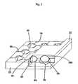
- FIG. 1depicts a portion of a light-emitting panel showing the basic socket structure of a socket formed from patterning a substrate, as disclosed in an embodiment of the present invention.
- FIG. 2depicts a portion of a light-emitting panel showing the basic socket structure of a socket formed from patterning a substrate, as disclosed in another embodiment of the present invention.
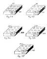
- FIG. 3Ashows an example of a cavity that has a cube shape.
- FIG. 3Bshows an example of a cavity that has a cone shape.
- FIG. 3Cshows an example of a cavity that has a conical frustum shape.
- FIG. 3Dshows an example of a cavity that has a paraboloid shape.
- FIG. 3Eshows an example of a cavity that has a spherical shape.
- FIG. 3Fshows an example of a cavity that has a cylindrical shape.
- FIG. 3Gshows an example of a cavity that has a pyramid shape.
- FIG. 3Hshows an example of a cavity that has a pyramidal frustum shape.
- FIG. 3Ishows an example of a cavity that has a parallelepiped shape.
- FIG. 3Jshows an example of a cavity that has a prism shape.
- FIG. 4shows the socket structure from a light-emitting panel of an embodiment of the present invention with a narrower field of view.
- FIG. 5shows the socket structure from a light-emitting panel of an embodiment of the present invention with a wider field of view.
- FIG. 6Adepicts a portion of a light-emitting panel showing the basic socket structure of a socket formed from disposing a plurality of material layers and then selectively removing a portion of the material layers with the electrodes having a co-planar configuration.
- FIG. 6Bis a cut-away of FIG. 6A showing in more detail the co-planar sustaining electrodes.
- FIG. 7Adepicts a portion of a light-emitting panel showing the basic socket structure of a socket formed from disposing a plurality of material layers and then selectively removing a portion of the material layers with the electrodes having a mid-plane configuration.
- FIG. 7Bis a cut-away of FIG. 7A showing in more detail the uppermost sustain electrode.
- FIG. 8depicts a portion of a light-emitting panel showing the basic socket structure of a socket formed from disposing a plurality of material layers and then selectively removing a portion of the material layers with the electrodes having an configuration with two sustain and two address electrodes, where the address electrodes are between the two, sustain electrodes.
- FIG. 9depicts a portion of a light-emitting panel showing the basic socket structure of a socket formed from patterning a substrate and then disposing a plurality of material layers on the substrate so that the material layers conform to the shape of the cavity with the electrodes having a co-planar configuration.
- FIG. 10depicts a portion of a light-emitting panel showing the basic socket structure of a socket formed from patterning a substrate and then disposing a plurality of material layers on the substrate so that the material layers conform to the shape of the cavity with the electrodes having a mid-plane configuration.
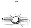
- FIG. 11depicts a portion of a light-emitting panel showing the basic socket structure of a socket formed from patterning a substrate and then disposing a plurality of material layers on the substrate so that the material layers conform to the shape of the cavity with the electrodes having a configuration with two sustain and two address electrodes, where the address electrodes are between the two sustain electrodes.
- FIG. 12shows a portion of a socket of an embodiment of the present invention where the micro-component and the cavity are formed as a type of male-female connector.
- FIG. 13shows an exploded view of a portion of a light-emitting panel showing the basic socket structure of a socket formed by disposing a plurality of material layers with aligned apertures on a substrate with the electrodes having a co-planar configuration.
- FIG. 14shows an exploded view of a portion of a light-emitting panel showing the basic socket structure of a socket formed by disposing a plurality of material layers with aligned apertures on a substrate with the electrodes having a mid-plane configuration.
- FIG. 15shows an exploded view of a portion of a light-emitting panel showing the basic socket structure of a socket formed by disposing a plurality of material layers with aligned apertures on a substrate with electrodes having a configuration with two sustain and two address electrodes, where the address electrodes are between the two sustain electrodes.
- the preferred embodiments of the present inventionare directed to a novel light-emitting panel.
- the preferred embodimentsare directed to a socket capable of being used in the light-emitting panel and supporting at least one micro-component.
- FIGS. 1 and 2show two embodiments of the present invention wherein a light-emitting panel includes a first substrate 10 and a second substrate 20 .
- the first substrate 10may be made from silicates, polypropylene, quartz, glass, any polymeric-based material or any material or combination of materials known to one skilled in the art.
- second substrate 20may be made from silicates, polypropylene, quartz, glass, any polymeric-based material or any material or combination of materials known to one skilled in the art.
- First substrate 10 and second substrate 20may both be made from the same material or each of a different material.
- the first and second substratemay be made of a material that dissipates heat from the light-emitting panel.
- each substrateis made from a material that is mechanically flexible.
- the first substrate 10includes a plurality of sockets 30 .
- the sockets 30may be disposed in any pattern, having uniform or non-uniform spacing between adjacent sockets. Patterns may include, but are not limited to, alphanumeric characters, symbols, icons, or pictures.
- the sockets 30are disposed in the first substrate 10 so that the distance between adjacent sockets 30 is approximately equal.
- Sockets 30may also be disposed in groups such that the distance between one group of sockets and another group of sockets is approximately equal. This latter approach may be particularly relevant in color light-emitting panels, where each socket in each group of sockets may represent red, green and blue, respectively.
- each socket 30At least partially disposed in each socket 30 is at least one micro-component 40 .
- Multiple micro-components 40may be disposed in a socket to provide increased luminosity and enhanced radiation transport efficiency.
- a single socketsupports three micro-components configured to emit red, green, and blue light, respectively.
- the micro-components 40may be of any shape, including, but not limited to, spherical, cylindrical, and aspherical.
- a micro-component 40includes a micro-component placed or formed inside another structure, such as placing a spherical micro-component inside a cylindrical-shaped structure.
- each cylindrical-shaped structuremay hold micro-components configured to emit a single color of visible light or multiple colors arranged red, green, blue, or in some other suitable color arrangement.
- each micro-component 40includes a shell 50 filled with a plasma-forming gas or gas mixture 45 .
- a plasma-forming gas or gas mixture 45is used in a preferred embodiment, any other material capable of providing luminescence is also contemplated, such as an electro-luminescent material, organic light-emitting diodes (OLEDs), or an electro-phoretic material.
- the shell 50may have a diameter ranging from micrometers to centimeters as measured across its minor axis, with virtually no limitation as to its size as measured across its major axis.
- a cylindrical-shaped micro-componentmay be only 100 microns in diameter across its minor axis, but may be hundreds of meters long across its major axis.
- the outside diameter of the shellis from 100 microns to 300 microns.
- the gas or gas mixtureionizes forming plasma and emitting radiation.
- a cavity 55 formed within and/or on a substrateprovides the basic socket 30 structure.
- the cavity 55may be any shape and size.
- the shape of the cavity 55may include, but is not limited to, a cube 100 , a cone 110 , a conical frustum 120 , a paraboloid 130 , spherical 140 , cylindrical 150 , a pyramid 160 , a pyramidal frustum 170 , a parallelepiped 180 , or a prism 190 .
- the socket 30may be formed as a type of male-female connector with a male micro-component 40 and a female cavity 55 .
- the male micro-component 40 and female cavity 55are formed to have complimentary shapes. As shown in FIG. 12 , as an example, both the cavity and micro-component have complimentary cylindrical shapes.
- the opening 35 of the female cavityis formed such that the opening is smaller than the diameter d of the male micro-component.
- the larger diameter male micro-componentcan be forced through the smaller opening of the female cavity 55 so that the male micro-component 40 is lockedlheld in the cavity and automatically aligned in the socket with respect to at least one electrode 500 disposed therein. This arrangement provides an added degree of flexibility for micro-component placement.
- this socket structureprovides a means by which cylindrical micro-components may be fed through the sockets on a row-by-row basis or in the case of a single long cylindrical micro-component (although other shapes would work equally well) fed/woven throughout the entire light-emitting panel.
- the size and shape of the socket 30influences the performance and characteristics of the light-emitting panel and are selected to optimize the panel's efficiency of operation.
- socket geometrymay be selected based on the shape and size of the micro-component to optimize the surface contact between the micro-component and the socket and/or to ensure connectivity of the micro-component and the electrodes disposed on or within the socket.
- the size and shape of the sockets 30may be chosen to optimize photon generation and provide increased luminosity and radiation transport efficiency.
- the size and shapemay be chosen to provide a field of view 400 with a specific angle ⁇ , such that a micro-component 40 disposed in a deep socket 30 may provide more collimated light and hence a narrower viewing angle ⁇ ( FIG. 4 ), while a micro-component 40 disposed in a shallow socket 30 may provide a wider viewing angle ⁇ ( FIG. 5 ).
- the cavitymay be sized, for example, so that its depth subsumes a micro-component that is deposited within a socket, or it may be made shallow so that a micro-component is only partially disposed within a socket.
- coatings 350that may be at least partially added to a socket that also influence the performance and characteristics of the light-emitting panel.
- Types of coatings 350include, but are not limited to, adhesives, bonding agents, coatings used to convert UV light to visible light, coatings used as reflecting filters, and coatings used as band-gap filters.
- the coatings 350may be applied to the inside of the socket 30 by differential stripping, lithographic process sputtering, laser deposition, chemical deposition, vapor deposition, or deposition using ink jet technology.
- differential strippinglithographic process sputtering, laser deposition, chemical deposition, vapor deposition, or deposition using ink jet technology.
- a micro-component 40may also be coated with a variety of coatings 300 .
- These micro-component coatings 300include, but are not limited to, coatings used to convert UV light to visible light, coatings used as reflecting filters, and coatings used as band-gap filters.
- a socket 30may contain a bonding agent or an adhesive.
- the bonding agent or adhesivemay readily hold a micro-component or plurality of micro-components in a socket or may require additional activation energy to secure the micro-components or plurality of micro-components in a socket.
- the inside of each of the sockets 30is at least partially coated with phosphor in order to convert the UV light to visible light.
- red, green, and blue phosphorsare used to create alternating red, green, and blue, pixels/subpixels, respectively. By combining these colors at varying intensities all colors can be formed.
- the phosphor coatingmay be combined with an adhesive so that the adhesive acts as a binder for the phosphor and also binds the micro-component 40 to the socket 30 when it is cured.
- the socket 30may be coated with a reflective material, including, but not limited to, optical dielectric stacks, to provide an increase in luminosity, by directing radiation traveling in the direction of the substrate in which the sockets are formed out through the field of view 400 of the light-emitting panel.
- a cavity 55is formed, or patterned, in a substrate 10 to create a basic socket shape.
- the cavitymay be formed in any suitable shape and size by any combination of physically, mechanically, thermally, electrically, optically, or chemically deforming the substrate.
- Disposed proximate to, and/or in, each socketmay be a variety of enhancement materials 325 .
- the enhancement materials 325include, but are not limited to, anti-glare coatings, touch sensitive surfaces, contrast enhancement coatings, protective coatings, transistors, integrated-circuits, semiconductor devices, inductors, capacitors, resistors, diodes, control electronics, drive electronics, pulse-forming networks, pulse compressors, pulse transformers, and tuned-circuits.
- a socket 30is formed by disposing a plurality of material layers 60 to form a first substrate 10 , disposing at least one electrode either directly on the first substrate 10 , within the material layers or any combination thereof, and selectively removing a portion of the material layers 60 to create a cavity.
- the material layers 60include any combination, in whole or in part, of dielectric materials, metals, and enhancement materials 325 .
- the enhancement materials 325include, but are not limited to, anti-glare coatings, touch sensitive surfaces, contrast enhancement coatings, protective coatings, transistors, integrated-circuits, semiconductor devices, inductors, capacitors, resistors, diodes, control electronics, drive electronics, pulse-forming networks, pulse compressors, pulse transformers, and tuned-circuits.
- the placement of the material layers 60may be accomplished by any transfer process, photolithography, sputtering, laser deposition, chemical deposition, vapor deposition, or deposition using ink jet technology.
- One of general skill in the artwill recognize other appropriate methods of disposing a plurality of material layers on a substrate.
- the cavity 55may be formed in the material layers 60 by a variety of methods including, but not limited to, wet or dry etching, photolithography, laser heat treatment, thermal form, mechanical punch, embossing, stamping-out, drilling, electroforming or by dimpling.
- a socket 30is formed by patterning a cavity 55 in a first substrate 10 , disposing a plurality of material layers 65 on the first substrate 10 so that the material layers 65 conform to the cavity 55 , and disposing at least one electrode on the first substrate 10 , within the material layers 65 , or any combination thereof.
- the cavitymay be formed in any suitable shape and size by any combination of physically, mechanically, thermally, electrically, optically, or chemically deforming the substrate.
- the material layers 65include any combination, in whole or in part, of dielectric materials, metals, and enhancement materials 325 .
- the enhancement materials 325include, but are not limited to, anti-glare coatings, touch sensitive surfaces, contrast enhancement coatings, protective coatings, transistors, integrated-circuits, semiconductor devices, inductors, capacitors, resistors, diodes, control electronics, drive electronics, pulse-forming networks, pulse compressors, pulse transformers, and tuned-circuits.
- the placement of the material layers 65may be accomplished by any transfer process, photolithography, sputtering, laser deposition, chemical deposition, vapor deposition, or deposition using ink jet technology.
- One of general skill in the artwill recognize other appropriate methods of disposing a plurality of material layers on a substrate.
- a socket 30is formed by disposing a plurality of material layers 66 on a first substrate 10 and disposing at least one electrode on the first substrate 10 , within the material layers 66 , or any combination thereof.
- Each of the material layersincludes a preformed aperture 56 that extends through the entire material layer.
- the aperturesmay be of the same size or may be of different sizes.
- the plurality of material layers 66are disposed on the first substrate with the apertures in alignment thereby forming a cavity 55 .
- the material layers 66include any combination, in whole or in part, of dielectric materials, metals, and enhancement materials 325 .
- the enhancement materials 325include, but are not limited to, anti-glare coatings, touch sensitive surfaces, contrast enhancement coatings, protective coatings, transistors, integrated-circuits, semiconductor devices, inductors, capacitors, resistors, diodes, control electronics, drive electronics, pulse-forming networks, pulse compressors, pulse transformers, and tuned-circuits.
- the placement of the material layers 66may be accomplished by any transfer process, photolithography, sputtering, laser deposition, chemical deposition, vapor deposition, or deposition using ink jet technology.
- One of general skill in the artwill recognize other appropriate methods of disposing a plurality of material layers on a substrate.
- a light-emitting panelincludes a plurality of electrodes, wherein at least two electrodes are adhered to only the first substrate, only the second substrate or at least one electrode is adhered to each of the first substrate and the second substrate and wherein the electrodes are arranged so that voltage applied to the electrodes causes one or more micro-components to emit radiation.
- a light-emitting panelincludes a plurality of electrodes, wherein at least two electrodes are arranged so that voltage supplied to the electrodes cause one or more micro-components to emit radiation throughout the field of view of the light-emitting panel without crossing either of the electrodes.
- At least two electrodesmay be disposed on the first substrate 10 , the second substrate 20 , or any combination thereof.
- a sustain electrode 70is adhered on the second substrate 20 and an address electrode 80 is adhered on the first substrate 10 .
- at least one electrode adhered to the first substrate 10is at least partly disposed within the socket ( FIGS. 1 and 2 ).
- the first substrate 10includes a plurality of material layers 60 and the cavities 55 are formed by selectively removing a portion of the material layers
- at least two electrodesmay be disposed on the first substrate 10 , disposed within the material layers 60 , disposed on the second substrate 20 , or any combination thereof.
- a first address electrode 80is disposed within the material layers 60
- a first sustain electrode 70is disposed within the material layers 60
- a second sustain electrode 75is disposed within the material layers 60 , such that the first sustain electrode and the second sustain electrode are in a co-planar configuration.
- FIG. 6Bis a cut-away of FIG. 6A showing the arrangement of the co-planar sustain electrodes 70 and 75 .
- a first sustain electrode 70is disposed on the first substrate 10
- a first address electrode 80is disposed within the material layers 60
- a second sustain electrode 75is disposed within the material layers 60 , such that the first address electrode is located between the first sustain electrode and the second sustain electrode in a mid-plane configuration.
- FIG. 7Bis a cut-away of FIG. 7A showing the first sustain electrode 70 . As seen in FIG.
- a first sustain electrode 70is disposed within the material layers 60
- a first address electrode 80is disposed within the material layers 60
- a second address electrode 85is disposed within the material layers 60
- a second sustain electrode 75is disposed within the material layers 60 , such that the first address electrode and the second address electrode are located between the first sustain electrode and the second sustain electrode.
- At least two electrodesmay be disposed on the first substrate 10 , at least partially disposed within the material layers 65 , disposed on the second substrate 20 , or any combination thereof.
- a first address electrode 80is disposed on the first substrate 10
- a first sustain electrode 70is disposed within the material layers 65
- a second sustain electrode 75is disposed within the material layers 65 , such that the first sustain electrode and the second sustain electrode are in a co-planar configuration.
- FIG. 9shows that the first sustain electrode and the second sustain electrode are in a co-planar configuration.
- a first sustain electrode 70is disposed on the first substrate 10
- a first address electrode 80is disposed within the material layers 65
- a second sustain electrode 75is disposed within the material layers 65 , such that the first address electrode is located between the first sustain electrode and the second sustain electrode in a mid-plane configuration.
- a first sustain electrode 70is disposed on the first substrate 10
- a first address electrode 80is disposed within the material layers 65
- a second address electrode 85is disposed within the material layers 65
- a second sustain electrode 75is disposed within the material layers 65 , such that the first address electrode and the second address electrode are located between the first sustain electrode and the second sustain electrode.
- At least two electrodesmay be disposed on the first substrate 10 , at least partially disposed within the material layers 65 , disposed on the second substrate 20 , or any combination thereof.
- a first address electrode 80is disposed on the first substrate 10
- a first sustain electrode 70is disposed within the material layers 66
- a second sustain electrode 75is disposed within the material layers 66 , such that the first sustain electrode and the second sustain electrode are in a co-planar configuration.
- FIG. 13shows that the first sustain electrode and the second sustain electrode are in a co-planar configuration.
- a first sustain electrode 70is disposed on the first substrate 10
- a first address electrode 80is disposed within the material layers 66
- a second sustain electrode 75is disposed within the material layers 66 , such that the first address electrode is located between the first sustain electrode and the second sustain electrode in a mid-plane configuration.
- a first sustain electrode 70is disposed on the first substrate 10
- a first address electrode 80is disposed within the material layers 66
- a second address electrode 85is disposed within the material layers 66
- a second sustain electrode 75is disposed within the material layers 66 , such that the first address electrode and the second address electrode are located between the first sustain electrode and the second sustain electrode.
Landscapes
- Engineering & Computer Science (AREA)
- Physics & Mathematics (AREA)
- Plasma & Fusion (AREA)
- Power Engineering (AREA)
- Computer Hardware Design (AREA)
- General Physics & Mathematics (AREA)
- Theoretical Computer Science (AREA)
- Devices For Indicating Variable Information By Combining Individual Elements (AREA)
- Gas-Filled Discharge Tubes (AREA)
- Vessels And Coating Films For Discharge Lamps (AREA)
- Electroluminescent Light Sources (AREA)
Abstract
Description
Claims (6)
Priority Applications (2)
| Application Number | Priority Date | Filing Date | Title |
|---|---|---|---|
| US11/135,538US7005793B2 (en) | 2000-10-27 | 2005-05-24 | Socket for use with a micro-component in a light-emitting panel |
| US11/313,745US20060097620A1 (en) | 2000-10-27 | 2005-12-22 | Socket for use with a micro-component in a light-emitting panel |
Applications Claiming Priority (4)
| Application Number | Priority Date | Filing Date | Title |
|---|---|---|---|
| US09/697,346US6545422B1 (en) | 2000-10-27 | 2000-10-27 | Socket for use with a micro-component in a light-emitting panel |
| US10/318,150US6646388B2 (en) | 2000-10-27 | 2002-12-13 | Socket for use with a micro-component in a light-emitting panel |
| US10/643,608US6902456B2 (en) | 2000-10-27 | 2003-08-20 | Socket for use with a micro-component in a light-emitting panel |
| US11/135,538US7005793B2 (en) | 2000-10-27 | 2005-05-24 | Socket for use with a micro-component in a light-emitting panel |
Related Parent Applications (1)
| Application Number | Title | Priority Date | Filing Date |
|---|---|---|---|
| US10/643,608DivisionUS6902456B2 (en) | 2000-10-27 | 2003-08-20 | Socket for use with a micro-component in a light-emitting panel |
Related Child Applications (1)
| Application Number | Title | Priority Date | Filing Date |
|---|---|---|---|
| US11/313,745ContinuationUS20060097620A1 (en) | 2000-10-27 | 2005-12-22 | Socket for use with a micro-component in a light-emitting panel |
Publications (2)
| Publication Number | Publication Date |
|---|---|
| US20050206317A1 US20050206317A1 (en) | 2005-09-22 |
| US7005793B2true US7005793B2 (en) | 2006-02-28 |
Family
ID=24800774
Family Applications (5)
| Application Number | Title | Priority Date | Filing Date |
|---|---|---|---|
| US09/697,346Expired - LifetimeUS6545422B1 (en) | 2000-10-27 | 2000-10-27 | Socket for use with a micro-component in a light-emitting panel |
| US10/318,150Expired - LifetimeUS6646388B2 (en) | 2000-10-27 | 2002-12-13 | Socket for use with a micro-component in a light-emitting panel |
| US10/643,608Expired - LifetimeUS6902456B2 (en) | 2000-10-27 | 2003-08-20 | Socket for use with a micro-component in a light-emitting panel |
| US11/135,538Expired - LifetimeUS7005793B2 (en) | 2000-10-27 | 2005-05-24 | Socket for use with a micro-component in a light-emitting panel |
| US11/313,745AbandonedUS20060097620A1 (en) | 2000-10-27 | 2005-12-22 | Socket for use with a micro-component in a light-emitting panel |
Family Applications Before (3)
| Application Number | Title | Priority Date | Filing Date |
|---|---|---|---|
| US09/697,346Expired - LifetimeUS6545422B1 (en) | 2000-10-27 | 2000-10-27 | Socket for use with a micro-component in a light-emitting panel |
| US10/318,150Expired - LifetimeUS6646388B2 (en) | 2000-10-27 | 2002-12-13 | Socket for use with a micro-component in a light-emitting panel |
| US10/643,608Expired - LifetimeUS6902456B2 (en) | 2000-10-27 | 2003-08-20 | Socket for use with a micro-component in a light-emitting panel |
Family Applications After (1)
| Application Number | Title | Priority Date | Filing Date |
|---|---|---|---|
| US11/313,745AbandonedUS20060097620A1 (en) | 2000-10-27 | 2005-12-22 | Socket for use with a micro-component in a light-emitting panel |
Country Status (7)
| Country | Link |
|---|---|
| US (5) | US6545422B1 (en) |
| EP (1) | EP1350238A4 (en) |
| JP (1) | JP2004531853A (en) |
| KR (1) | KR100881154B1 (en) |
| CN (2) | CN100365678C (en) |
| AU (1) | AU2001297560A1 (en) |
| WO (1) | WO2002075706A2 (en) |
Cited By (39)
| Publication number | Priority date | Publication date | Assignee | Title |
|---|---|---|---|---|
| US20050095944A1 (en)* | 2000-10-27 | 2005-05-05 | Science Applications International Corporation | Design, fabrication, testing, and conditioning of micro-components for use in a light-emitting panel |
| US7122961B1 (en) | 2002-05-21 | 2006-10-17 | Imaging Systems Technology | Positive column tubular PDP |
| US7157854B1 (en) | 2002-05-21 | 2007-01-02 | Imaging Systems Technology | Tubular PDP |
| US7288014B1 (en)* | 2000-10-27 | 2007-10-30 | Science Applications International Corporation | Design, fabrication, testing, and conditioning of micro-components for use in a light-emitting panel |
| US7405516B1 (en) | 2004-04-26 | 2008-07-29 | Imaging Systems Technology | Plasma-shell PDP with organic luminescent substance |
| US7535175B1 (en) | 2006-02-16 | 2009-05-19 | Imaging Systems Technology | Electrode configurations for plasma-dome PDP |
| US7604523B1 (en) | 2004-06-21 | 2009-10-20 | Imaging Systems Technology | Plasma-shell PDP |
| US7622866B1 (en) | 2005-02-22 | 2009-11-24 | Imaging Systems Technology | Plasma-dome PDP |
| US7628666B1 (en) | 2002-05-21 | 2009-12-08 | Imaging Systems Technology | Process for manufacturing plasma-dome PDP |
| US7638943B1 (en) | 2002-05-21 | 2009-12-29 | Imaging Systems Technology | Plasma-disc article of manufacture |
| US7679286B1 (en) | 2002-05-21 | 2010-03-16 | Imaging Systems Technology | Positive column tubular PDP |
| US7727040B1 (en) | 2002-05-21 | 2010-06-01 | Imaging Systems Technology | Process for manufacturing plasma-disc PDP |
| US7730746B1 (en) | 2005-07-14 | 2010-06-08 | Imaging Systems Technology | Apparatus to prepare discrete hollow microsphere droplets |
| US7772774B1 (en) | 2002-05-21 | 2010-08-10 | Imaging Systems Technology | Positive column plasma display tubular device |
| US7772773B1 (en) | 2003-11-13 | 2010-08-10 | Imaging Systems Technology | Electrode configurations for plasma-dome PDP |
| US7791037B1 (en) | 2006-03-16 | 2010-09-07 | Imaging Systems Technology | Plasma-tube radiation detector |
| US7863815B1 (en) | 2006-01-26 | 2011-01-04 | Imaging Systems Technology | Electrode configurations for plasma-disc PDP |
| US7923930B1 (en) | 2000-01-12 | 2011-04-12 | Imaging Systems Technology | Plasma-shell device |
| US7932674B1 (en) | 2002-05-21 | 2011-04-26 | Imaging Systems Technology | Plasma-dome article of manufacture |
| US7969092B1 (en) | 2000-01-12 | 2011-06-28 | Imaging Systems Technology, Inc. | Gas discharge display |
| US8035303B1 (en) | 2006-02-16 | 2011-10-11 | Imaging Systems Technology | Electrode configurations for gas discharge device |
| US8106586B1 (en) | 2004-04-26 | 2012-01-31 | Imaging Systems Technology, Inc. | Plasma discharge display with fluorescent conversion material |
| US8110987B1 (en) | 2002-05-21 | 2012-02-07 | Imaging Systems Technology, Inc. | Microshell plasma display |
| US8113898B1 (en) | 2004-06-21 | 2012-02-14 | Imaging Systems Technology, Inc. | Gas discharge device with electrical conductive bonding material |
| US8129906B1 (en) | 2004-04-26 | 2012-03-06 | Imaging Systems Technology, Inc. | Lumino-shells |
| US8138673B1 (en) | 2002-05-21 | 2012-03-20 | Imaging Systems Technology | Radiation shielding |
| US8198811B1 (en) | 2002-05-21 | 2012-06-12 | Imaging Systems Technology | Plasma-Disc PDP |
| US8198812B1 (en) | 2002-05-21 | 2012-06-12 | Imaging Systems Technology | Gas filled detector shell with dipole antenna |
| US8232725B1 (en) | 2002-05-21 | 2012-07-31 | Imaging Systems Technology | Plasma-tube gas discharge device |
| US8278824B1 (en) | 2006-02-16 | 2012-10-02 | Imaging Systems Technology, Inc. | Gas discharge electrode configurations |
| US8299696B1 (en) | 2005-02-22 | 2012-10-30 | Imaging Systems Technology | Plasma-shell gas discharge device |
| US8339041B1 (en) | 2004-04-26 | 2012-12-25 | Imaging Systems Technology, Inc. | Plasma-shell gas discharge device with combined organic and inorganic luminescent substances |
| US8368303B1 (en) | 2004-06-21 | 2013-02-05 | Imaging Systems Technology, Inc. | Gas discharge device with electrical conductive bonding material |
| US8410695B1 (en) | 2006-02-16 | 2013-04-02 | Imaging Systems Technology | Gas discharge device incorporating gas-filled plasma-shell and method of manufacturing thereof |
| US8513887B1 (en) | 2002-05-21 | 2013-08-20 | Imaging Systems Technology, Inc. | Plasma-dome article of manufacture |
| US8618733B1 (en) | 2006-01-26 | 2013-12-31 | Imaging Systems Technology, Inc. | Electrode configurations for plasma-shell gas discharge device |
| US8951608B1 (en) | 2004-10-22 | 2015-02-10 | Imaging Systems Technology, Inc. | Aqueous manufacturing process and article |
| US9013102B1 (en) | 2009-05-23 | 2015-04-21 | Imaging Systems Technology, Inc. | Radiation detector with tiled substrates |
| US9229937B2 (en) | 2006-04-06 | 2016-01-05 | Samsung Electronics Co., Ltd. | Apparatus and method for managing digital contents distributed over network |
Families Citing this family (39)
| Publication number | Priority date | Publication date | Assignee | Title |
|---|---|---|---|---|
| US7619591B1 (en)* | 1999-04-26 | 2009-11-17 | Imaging Systems Technology | Addressing and sustaining of plasma display with plasma-shells |
| US7595774B1 (en)* | 1999-04-26 | 2009-09-29 | Imaging Systems Technology | Simultaneous address and sustain of plasma-shell display |
| US6864631B1 (en)* | 2000-01-12 | 2005-03-08 | Imaging Systems Technology | Gas discharge display device |
| US6762566B1 (en)* | 2000-10-27 | 2004-07-13 | Science Applications International Corporation | Micro-component for use in a light-emitting panel |
| US6612889B1 (en)* | 2000-10-27 | 2003-09-02 | Science Applications International Corporation | Method for making a light-emitting panel |
| US6764367B2 (en) | 2000-10-27 | 2004-07-20 | Science Applications International Corporation | Liquid manufacturing processes for panel layer fabrication |
| WO2002082253A2 (en)* | 2001-04-04 | 2002-10-17 | Elo Touchsystems, Inc. | A touch input system |
| US6739932B2 (en)* | 2001-06-07 | 2004-05-25 | Si Diamond Technology, Inc. | Field emission display using carbon nanotubes and methods of making the same |
| JP4506070B2 (en)* | 2002-11-01 | 2010-07-21 | コニカミノルタホールディングス株式会社 | Method for forming antiglare layer, method for producing antiglare film, and ink jet device for forming antiglare layer |
| US7298078B2 (en)* | 2004-01-14 | 2007-11-20 | E-Lite Technologies, Inc. | Flat, flexible fluorescent lamp |
| US20050189164A1 (en)* | 2004-02-26 | 2005-09-01 | Chang Chi L. | Speaker enclosure having outer flared tube |
| TWI367686B (en)* | 2004-04-07 | 2012-07-01 | Semiconductor Energy Lab | Light emitting device, electronic device, and television device |
| US8981645B1 (en)* | 2004-06-21 | 2015-03-17 | Imaging Systems Technology, Inc. | Gas discharge device with electrical conductive bonding material |
| US20080012461A1 (en)* | 2004-11-09 | 2008-01-17 | Nano-Proprietary, Inc. | Carbon nanotube cold cathode |
| US9153163B2 (en)* | 2005-03-11 | 2015-10-06 | The Invention Science Fund I, Llc | Self assembly of elements for displays |
| US20060202944A1 (en)* | 2005-03-11 | 2006-09-14 | Searete Llc, A Limited Liability Corporation Of The State Of Delaware | Elements for self assembling displays |
| US7977130B2 (en)* | 2006-08-03 | 2011-07-12 | The Invention Science Fund I, Llc | Method of assembling displays on substrates |
| US7990349B2 (en)* | 2005-04-22 | 2011-08-02 | The Invention Science Fund I, Llc | Superimposed displays |
| US8300007B2 (en)* | 2005-03-11 | 2012-10-30 | The Invention Science Fund I, Llc | Self assembling display with substrate |
| US8390537B2 (en)* | 2005-03-11 | 2013-03-05 | The Invention Science Fund I, Llc | Method of assembling displays on substrates |
| US8860635B2 (en)* | 2005-04-04 | 2014-10-14 | The Invention Science Fund I, Llc | Self assembling display with substrate |
| US8711063B2 (en) | 2005-03-11 | 2014-04-29 | The Invention Science Fund I, Llc | Self assembly of elements for displays |
| US7662008B2 (en)* | 2005-04-04 | 2010-02-16 | Searete Llc | Method of assembling displays on substrates |
| US8334819B2 (en)* | 2005-03-11 | 2012-12-18 | The Invention Science Fund I, Llc | Superimposed displays |
| US7375342B1 (en)* | 2005-03-22 | 2008-05-20 | Imaging Systems Technology | Plasma-shell radiation detector |
| US7476867B2 (en)* | 2005-05-27 | 2009-01-13 | Iba | Device and method for quality assurance and online verification of radiation therapy |
| JPWO2006134660A1 (en)* | 2005-06-17 | 2009-01-08 | 篠田プラズマ株式会社 | Discharge tube array and display device using the same |
| US20070040503A1 (en)* | 2005-08-18 | 2007-02-22 | Charles Chase | Microstructure non-thermal visible light source |
| KR100738226B1 (en)* | 2005-09-27 | 2007-07-12 | 엘지전자 주식회사 | Electroluminescent display |
| KR20070046613A (en)* | 2005-10-31 | 2007-05-03 | 삼성에스디아이 주식회사 | Plasma display panel |
| US20080029775A1 (en)* | 2006-08-02 | 2008-02-07 | Lustrous Technology Ltd. | Light emitting diode package with positioning groove |
| WO2008064712A1 (en)* | 2006-11-27 | 2008-06-05 | Osram Gesellschaft mit beschränkter Haftung | Discharge lamp system |
| US20080315108A1 (en)* | 2007-06-19 | 2008-12-25 | Stephan Andrew C | Neutron detector |
| US7923698B2 (en)* | 2007-06-19 | 2011-04-12 | Material Innovations, Inc. | Neutron detector |
| US7514694B2 (en)* | 2007-06-19 | 2009-04-07 | Material Innovations, Inc. | Neutron detector |
| US7919758B2 (en)* | 2007-06-19 | 2011-04-05 | Material Innovations, Inc. | Neutron detector |
| TWI522563B (en)* | 2012-02-16 | 2016-02-21 | 陞泰科技股份有限公司 | Variable light beam led and method thereof |
| US11391437B2 (en) | 2018-01-30 | 2022-07-19 | Brightview Technologies, Inc. | Microstructures for transforming light having Lambertian distribution into batwing distributions |
| CN221079143U (en) | 2023-05-22 | 2024-06-04 | 亮视技术公司 | Backlight unit |
Citations (146)
| Publication number | Priority date | Publication date | Assignee | Title |
|---|---|---|---|---|
| US3559190A (en) | 1966-01-18 | 1971-01-26 | Univ Illinois | Gaseous display and memory apparatus |
| US3646384A (en) | 1970-06-09 | 1972-02-29 | Ibm | One-sided plasma display panel |
| US3704052A (en) | 1971-05-03 | 1972-11-28 | Ncr Co | Method of making a plasma display panel |
| US3755027A (en) | 1970-11-19 | 1973-08-28 | Philips Corp | Method of manufacturing a gas discharge panel and panel manufactured by said method |
| US3848248A (en) | 1972-02-10 | 1974-11-12 | Sanders Associates Inc | Gaseous discharge device |
| US3969651A (en) | 1974-12-30 | 1976-07-13 | Ibm Corporation | Display system |
| US3990068A (en) | 1976-01-26 | 1976-11-02 | Control Data Corporation | Plasma display panel drive system |
| US3998618A (en) | 1975-11-17 | 1976-12-21 | Sanders Associates, Inc. | Method for making small gas-filled beads |
| US4027246A (en) | 1976-03-26 | 1977-05-31 | International Business Machines Corporation | Automated integrated circuit manufacturing system |
| US4035690A (en) | 1974-10-25 | 1977-07-12 | Raytheon Company | Plasma panel display device including spheroidal glass shells |
| US4303433A (en) | 1978-08-28 | 1981-12-01 | Torobin Leonard B | Centrifuge apparatus and method for producing hollow microspheres |
| US4379301A (en) | 1981-09-22 | 1983-04-05 | Xerox Corporation | Method for ink jet printing |
| US4386358A (en) | 1981-09-22 | 1983-05-31 | Xerox Corporation | Ink jet printing using electrostatic deflection |
| US4393326A (en) | 1980-02-22 | 1983-07-12 | Okaya Electric Industries Co., Ltd. | DC Plasma display panel |
| US4429303A (en) | 1980-12-22 | 1984-01-31 | International Business Machines Corporation | Color plasma display device |
| US4534743A (en) | 1983-08-31 | 1985-08-13 | Timex Corporation | Process for making an electroluminescent lamp |
| US4554537A (en) | 1982-10-27 | 1985-11-19 | At&T Bell Laboratories | Gas plasma display |
| US4563617A (en) | 1983-01-10 | 1986-01-07 | Davidson Allen S | Flat panel television/display |
| US4591847A (en) | 1969-12-15 | 1986-05-27 | International Business Machines Corporation | Method and apparatus for gas display panel |
| US4654561A (en) | 1985-10-07 | 1987-03-31 | Shelton Jay D | Plasma containment device |
| US4658269A (en) | 1986-06-02 | 1987-04-14 | Xerox Corporation | Ink jet printer with integral electrohydrodynamic electrodes and nozzle plate |
| US4697123A (en) | 1980-11-19 | 1987-09-29 | Fujitsu Limited | Gas discharge panel |
| US4728864A (en) | 1986-03-03 | 1988-03-01 | American Telephone And Telegraph Company, At&T Bell Laboratories | AC plasma display |
| US4833463A (en) | 1986-09-26 | 1989-05-23 | American Telephone And Telegraph Company, At&T Bell Laboratories | Gas plasma display |
| US4843281A (en) | 1986-10-17 | 1989-06-27 | United Technologies Corporation | Gas plasma panel |
| US4887003A (en) | 1988-05-10 | 1989-12-12 | Parker William P | Screen printable luminous panel display device |
| US4912364A (en) | 1987-07-16 | 1990-03-27 | Tungsram Reszvenytarsasag | Three-phase high-pressure gas discharge lamp filled with a gas containing sodium or a metal-halide |
| US5019807A (en) | 1984-07-25 | 1991-05-28 | Staplevision, Inc. | Display screen |
| US5030888A (en) | 1988-08-26 | 1991-07-09 | Thomson-Csf | Very fast method of control by semi-selective and selective addressing of a coplanar sustaining AC type of plasma panel |
| US5062916A (en) | 1990-08-01 | 1991-11-05 | W. H. Brady Co. | Method for the manufacture of electrical membrane panels having circuits on flexible plastic films |
| US5068916A (en) | 1990-10-29 | 1991-11-26 | International Business Machines Corporation | Coordination of wireless medium among a plurality of base stations |
| US5075597A (en) | 1988-08-26 | 1991-12-24 | Thomson-Csf | Method for the row-by-row control of a coplanar sustaining ac type of plasma panel |
| US5126632A (en) | 1988-05-10 | 1992-06-30 | Parker William P | Luminous panel display device |
| US5150007A (en) | 1990-05-11 | 1992-09-22 | Bell Communications Research, Inc. | Non-phosphor full-color plasma display device |
| JPH04287397A (en) | 1991-03-18 | 1992-10-12 | Nec Corp | Mounting structure for outer lead connecting substrate of display element |
| US5315129A (en) | 1990-08-20 | 1994-05-24 | University Of Southern California | Organic optoelectronic devices and methods |
| US5396149A (en) | 1991-09-28 | 1995-03-07 | Samsung Electron Devices Co., Ltd. | Color plasma display panel |
| US5500287A (en) | 1992-10-30 | 1996-03-19 | Innovation Associates, Inc. | Thermal insulating material and method of manufacturing same |
| US5510678A (en) | 1991-07-18 | 1996-04-23 | Nippon Hoso Kyokai | DC type gas-discharge display panel and gas-discharge display apparatus with employment of the same |
| US5514934A (en) | 1991-05-31 | 1996-05-07 | Mitsubishi Denki Kabushiki Kaisha | Discharge lamp, image display device using the same and discharge lamp producing method |
| US5674351A (en) | 1992-04-10 | 1997-10-07 | Candescent Technologies Corporation | Self supporting flat video display |
| US5675212A (en) | 1992-04-10 | 1997-10-07 | Candescent Technologies Corporation | Spacer structures for use in flat panel displays and methods for forming same |
| US5686790A (en) | 1993-06-22 | 1997-11-11 | Candescent Technologies Corporation | Flat panel device with ceramic backplate |
| US5703436A (en) | 1994-12-13 | 1997-12-30 | The Trustees Of Princeton University | Transparent contacts for organic devices |
| JPH103869A (en) | 1997-03-26 | 1998-01-06 | Canon Inc | Light emitting device and image display device |
| US5707745A (en) | 1994-12-13 | 1998-01-13 | The Trustees Of Princeton University | Multicolor organic light emitting devices |
| US5725787A (en) | 1992-04-10 | 1998-03-10 | Candescent Technologies Corporation | Fabrication of light-emitting device with raised black matrix for use in optical devices such as flat-panel cathode-ray tubes |
| US5747931A (en) | 1996-05-24 | 1998-05-05 | David Sarnoff Research Center, Inc. | Plasma display and method of making same |
| US5746635A (en) | 1992-04-10 | 1998-05-05 | Candescent Technologies Corporation | Methods for fabricating a flat panel display having high voltage supports |
| US5757131A (en) | 1995-08-11 | 1998-05-26 | Nec Corporation | Color plasma display panel and fabricating method |
| US5757139A (en) | 1997-02-03 | 1998-05-26 | The Trustees Of Princeton University | Driving circuit for stacked organic light emitting devices |
| US5755944A (en) | 1996-06-07 | 1998-05-26 | Candescent Technologies Corporation | Formation of layer having openings produced by utilizing particles deposited under influence of electric field |
| US5777782A (en) | 1996-12-24 | 1998-07-07 | Xerox Corporation | Auxiliary optics for a twisting ball display |
| US5788814A (en) | 1996-04-09 | 1998-08-04 | David Sarnoff Research Center | Chucks and methods for positioning multiple objects on a substrate |
| US5793158A (en) | 1992-08-21 | 1998-08-11 | Wedding, Sr.; Donald K. | Gas discharge (plasma) displays |
| US5808403A (en) | 1994-08-05 | 1998-09-15 | Pixel International S.A. | Microtip cathode with auxiliary insulating layer |
| US5811833A (en) | 1996-12-23 | 1998-09-22 | University Of So. Ca | Electron transporting and light emitting layers based on organic free radicals |
| US5815306A (en) | 1996-12-24 | 1998-09-29 | Xerox Corporation | "Eggcrate" substrate for a twisting ball display |
| US5825451A (en) | 1997-10-17 | 1998-10-20 | Advanced Display Systems, Inc. | Methods of manufacturing multi-color liquid crystal displays using in situ mixing techniques |
| US5837221A (en) | 1996-07-29 | 1998-11-17 | Acusphere, Inc. | Polymer-lipid microencapsulated gases for use as imaging agents |
| US5844363A (en) | 1997-01-23 | 1998-12-01 | The Trustees Of Princeton Univ. | Vacuum deposited, non-polymeric flexible organic light emitting devices |
| US5853446A (en) | 1996-04-16 | 1998-12-29 | Corning Incorporated | Method for forming glass rib structures |
| US5862054A (en) | 1997-02-20 | 1999-01-19 | Taiwan Semiconductor Manufacturing Company, Ltd. | Process monitoring system for real time statistical process control |
| US5865657A (en) | 1996-06-07 | 1999-02-02 | Candescent Technologies Corporation | Fabrication of gated electron-emitting device utilizing distributed particles to form gate openings typically beveled and/or combined with lift-off or electrochemical removal of excess emitter material |
| US5897414A (en) | 1995-10-24 | 1999-04-27 | Candescent Technologies Corporation | Technique for increasing manufacturing yield of matrix-addressable device |
| US5898266A (en) | 1996-07-18 | 1999-04-27 | Candescent Technologies Corporation | Method for displaying frame of pixel information on flat panel display |
| US5913704A (en) | 1993-09-08 | 1999-06-22 | Candescent Technologies Corporation | Fabrication of electronic devices by method that involves ion tracking |
| US5914150A (en) | 1997-02-28 | 1999-06-22 | Candescent Technologies Corporation | Formation of polycarbonate film with apertures determined by etching charged-particle tracks |
| US5917646A (en) | 1996-12-24 | 1999-06-29 | Xerox Corporation | Rotatable lens transmissive twisting ball display |
| US5920080A (en) | 1997-06-23 | 1999-07-06 | Fed Corporation | Emissive display using organic light emitting diodes |
| US5945174A (en) | 1995-04-06 | 1999-08-31 | Delta V Technologies, Inc. | Acrylate polymer release coated sheet materials and method of production thereof |
| US5953587A (en) | 1997-11-24 | 1999-09-14 | The Trustees Of Princeton University | Method for deposition and patterning of organic thin film |
| US5964630A (en) | 1996-12-23 | 1999-10-12 | Candescent Technologies Corporation | Method of increasing resistance of flat-panel device to bending, and associated getter-containing flat-panel device |
| US5965109A (en) | 1994-08-02 | 1999-10-12 | Molecular Biosystems, Inc. | Process for making insoluble gas-filled microspheres containing a liquid hydrophobic barrier |
| US5967871A (en) | 1997-07-24 | 1999-10-19 | Photonics Systems, Inc. | Method for making back glass substrate for plasma display panel |
| US5969472A (en) | 1997-12-03 | 1999-10-19 | Lockheed Martin Energy Research Corporation | Lighting system of encapsulated luminous material |
| US5975683A (en) | 1995-06-07 | 1999-11-02 | Xerox Corporation | Electric-field manipulation of ejected ink drops in printing |
| US5984747A (en) | 1996-03-28 | 1999-11-16 | Corning Incorporated | Glass structures for information displays |
| US5986409A (en) | 1998-03-30 | 1999-11-16 | Micron Technology, Inc. | Flat panel display and method of its manufacture |
| US5985460A (en) | 1994-12-05 | 1999-11-16 | E. I. Du Pont De Nemours And Company | Insulator composition, green tape, and method for forming plasma display apparatus barrier-rib |
| US5990620A (en) | 1997-09-30 | 1999-11-23 | Lepselter; Martin P. | Pressurized plasma display |
| US5990614A (en) | 1998-02-27 | 1999-11-23 | Candescent Technologies Corporation | Flat-panel display having temperature-difference accommodating spacer system |
| US6013538A (en) | 1997-11-24 | 2000-01-11 | The Trustees Of Princeton University | Method of fabricating and patterning OLEDs |
| US6017584A (en) | 1995-07-20 | 2000-01-25 | E Ink Corporation | Multi-color electrophoretic displays and materials for making the same |
| US6019657A (en) | 1997-09-17 | 2000-02-01 | Candescent Technologies Corporation | Dual-layer metal for flat panel display |
| US6023259A (en) | 1997-07-11 | 2000-02-08 | Fed Corporation | OLED active matrix using a single transistor current mode pixel design |
| US6022652A (en) | 1994-11-21 | 2000-02-08 | Candescent Technologies Corporation | High resolution flat panel phosphor screen with tall barriers |
| US6025097A (en) | 1997-02-28 | 2000-02-15 | Candescent Technologies Corporation | Method for creating a color filter layer on a field emission display screen structure |
| US6030715A (en) | 1997-10-09 | 2000-02-29 | The University Of Southern California | Azlactone-related dopants in the emissive layer of an OLED |
| US6030269A (en) | 1997-03-31 | 2000-02-29 | Candescent Technologies Corporation | Method for forming a multi-level conductive black matrix for a flat panel display |
| US6033547A (en) | 1996-11-26 | 2000-03-07 | The Trustees Of Princeton University | Apparatus for electrohydrodynamically assembling patterned colloidal structures |
| US6037918A (en) | 1998-03-30 | 2000-03-14 | Candescent Technologies, Inc. | Error compensator circuits used in color balancing with time multiplexed voltage signals for a flat panel display unit |
| US6038002A (en) | 1996-07-13 | 2000-03-14 | Lg Electronics Inc. | Thin film transistor liquid crystal display and method for fabricating the same |
| US6037710A (en) | 1998-04-29 | 2000-03-14 | Candescent Technologies, Inc. | Microwave sealing of flat panel displays |
| US6039619A (en) | 1997-05-22 | 2000-03-21 | Samsung Display Devices Co., Ltd. | Method and apparatus for manufacturing partition wall of plasma display device |
| US6046543A (en) | 1996-12-23 | 2000-04-04 | The Trustees Of Princeton University | High reliability, high efficiency, integratable organic light emitting devices and methods of producing same |
| US6045930A (en) | 1996-12-23 | 2000-04-04 | The Trustees Of Princeton University | Materials for multicolor light emitting diodes |
| US6049366A (en) | 1995-06-09 | 2000-04-11 | Sniaricerche S.C.P.A. | Polymer stabilized liquid crystals and flexible devices thereof |
| US6048630A (en) | 1996-07-02 | 2000-04-11 | The Trustees Of Princeton University | Red-emitting organic light emitting devices (OLED's) |
| US6048469A (en) | 1997-02-26 | 2000-04-11 | The Regents Of The University Of California | Advanced phosphors |
| US6069443A (en) | 1997-06-23 | 2000-05-30 | Fed Corporation | Passive matrix OLED display |
| US6072276A (en) | 1996-06-21 | 2000-06-06 | Nec Corporation | Color plasma display panel and method of manufacturing the same |
| WO2000036465A1 (en) | 1998-12-15 | 2000-06-22 | E Ink Corporation | Assembly of microencapsulated electronic display |
| US6079814A (en) | 1997-06-27 | 2000-06-27 | Xerox Corporation | Ink jet printer having improved ink droplet placement |
| US6080606A (en) | 1996-03-26 | 2000-06-27 | The Trustees Of Princeton University | Electrophotographic patterning of thin film circuits |
| US6087196A (en) | 1998-01-30 | 2000-07-11 | The Trustees Of Princeton University | Fabrication of organic semiconductor devices using ink jet printing |
| US6091380A (en) | 1996-06-18 | 2000-07-18 | Mitsubishi Denki Kabushiki Kaisha | Plasma display |
| US6091874A (en) | 1997-07-14 | 2000-07-18 | Tomoegawa Paper Co., Ltd. | Flexible optical waveguide device and process for the production thereof |
| US6091195A (en) | 1997-02-03 | 2000-07-18 | The Trustees Of Princeton University | Displays having mesa pixel configuration |
| US6097147A (en) | 1998-09-14 | 2000-08-01 | The Trustees Of Princeton University | Structure for high efficiency electroluminescent device |
| US6130655A (en) | 1996-03-18 | 2000-10-10 | U.S. Philips Corporation | Plasma-addressed display |
| US6137553A (en) | 1997-10-08 | 2000-10-24 | Sharp Kabushiki Kaisha | Display device and manufacturing method thereof |
| US6201518B1 (en) | 1997-09-26 | 2001-03-13 | Sarnoff Corporation | Continuous drive AC plasma display device |
| US6255777B1 (en) | 1998-07-01 | 2001-07-03 | Plasmion Corporation | Capillary electrode discharge plasma display panel device and method of fabricating the same |
| US6262706B1 (en) | 1995-07-20 | 2001-07-17 | E Ink Corporation | Retroreflective electrophoretic displays and materials for making the same |
| US20010008825A1 (en) | 1996-08-11 | 2001-07-19 | Osamu Toyoda | Method of manufacturing panel assembly used to assemble display panel and transfer material sheet |
| US6265826B1 (en) | 1998-09-11 | 2001-07-24 | Sony Corporation | Plasma addressing display device |
| US6281863B1 (en) | 1995-11-15 | 2001-08-28 | Hitachi, Ltd. | Plasma display panel driving system and method |
| US6285434B1 (en) | 1998-02-20 | 2001-09-04 | Advanced Display Systems, Inc. | Substrate for colored cholesteric liquid crystal display allowing cholesteric liquid crystal material to be filled by surface tension without vacuum |
| US6285129B1 (en) | 1997-05-12 | 2001-09-04 | Samsung Display Devices Co., Ltd. | Helium plasma display device |
| US6288693B1 (en) | 1996-11-30 | 2001-09-11 | Lg Electronics Inc. | Plasma display panel driving method |
| US6288488B1 (en) | 1997-11-13 | 2001-09-11 | Pioneer Electronic Corporation | Plasma display panel having particular structure of electrodes |
| US6292159B1 (en) | 1997-05-08 | 2001-09-18 | Mitsubishi Denki Kabushiki Kaisha | Method for driving plasma display panel |
| US6291925B1 (en) | 1998-01-12 | 2001-09-18 | Massachusetts Institute Of Technology | Apparatus and methods for reversible imaging of nonemissive display systems |
| US6292160B1 (en) | 1997-05-20 | 2001-09-18 | Samsung Display Devices, Ltd. | Plasma display panel and driving method thereof |
| US6295040B1 (en) | 1995-10-16 | 2001-09-25 | Fujitsu Limited | AC-type plasma display panel and its driving method |
| US6296539B1 (en) | 1997-02-24 | 2001-10-02 | Fujitsu Limited | Method of making plasma display panel with dielectric layer suppressing reduced electrode conductivity |
| US6297590B1 (en) | 1995-08-25 | 2001-10-02 | Fujitsu Limited | Surface discharge plasma display panel |
| US6300932B1 (en) | 1997-08-28 | 2001-10-09 | E Ink Corporation | Electrophoretic displays with luminescent particles and materials for making the same |
| US6300152B1 (en) | 1999-06-30 | 2001-10-09 | Samsung Electronics Co., Ltd. | Method for manufacturing a panel for a liquid crystal display with a plasma-treated organic insulating layer |
| US6304032B1 (en) | 1998-06-24 | 2001-10-16 | Nec Corporation | Plasma display panel and method of producing the same |
| US6304031B1 (en) | 1997-08-01 | 2001-10-16 | Matsushita Electric Industrial Co., Ltd. | Plasma display panel |
| US6304238B1 (en) | 1998-08-25 | 2001-10-16 | Sony Corporation | Driving apparatus for plasma addressed liquid crystal display apparatus |
| US6307319B1 (en) | 1999-12-28 | 2001-10-23 | Samsung Sdi Co., Ltd. | Plasma display panel and method for manufacturing the same |
| US20010033256A1 (en) | 2000-03-01 | 2001-10-25 | Moore Chad Byron | Medium and large pixel multiple strand array structure plasma display |
| US6312971B1 (en) | 1999-08-31 | 2001-11-06 | E Ink Corporation | Solvent annealing process for forming a thin semiconductor film with advantageous properties |
| US6319325B1 (en) | 1999-02-26 | 2001-11-20 | Sony Corporation | Apparatus for producing thin film, process for producing thin film and guide roller |
| US6322010B1 (en) | 1998-12-25 | 2001-11-27 | Sony Corporation | Paint coating apparatus and magnetic recording medium |
| US20010053570A1 (en) | 2000-06-12 | 2001-12-20 | Nec Corporation | Pattern formation method and method of manufacturing display using it |
| US20020008470A1 (en) | 2000-05-23 | 2002-01-24 | Hiroko Uegaki | Paste, display member, and process for production of display member |
| US20020009536A1 (en) | 1996-12-17 | 2002-01-24 | Yuichiro Iguchi | Method and apparatus for producing a plasma display |
| US20020016075A1 (en) | 2000-08-04 | 2002-02-07 | Hannstar Display Corp. | Method of patterning an ITO layer |
| US20020017864A1 (en) | 1999-02-12 | 2002-02-14 | Toppan Printing Co., Ltd. | Plasma display panel, manufacturing method and manufacturing apparatus of the same |
| US20020022565A1 (en) | 2000-05-02 | 2002-02-21 | Sreeram Attiganal Narayanaswamy | Materials to fabricate a high resolution plasma display back panel |
| US20020024295A1 (en) | 2000-04-04 | 2002-02-28 | Kanako Miyashita | Highly productive method of producing plasma display panel |
| US6459201B1 (en)* | 1999-08-17 | 2002-10-01 | Lg Electronics Inc. | Flat-panel display with controlled sustaining electrodes |
Family Cites Families (17)
| Publication number | Priority date | Publication date | Assignee | Title |
|---|---|---|---|---|
| US1961735A (en)* | 1928-08-17 | 1934-06-05 | Gen Electric Vapor Lamp Co | Electric sign |
| US1923148A (en)* | 1929-10-05 | 1933-08-22 | Hotchner Fred | Method and means of fabricating tubing of vitreous material |
| US2036616A (en)* | 1935-02-13 | 1936-04-07 | Joseph C Asch | Lighting device |
| US3453478A (en)* | 1966-05-31 | 1969-07-01 | Stanford Research Inst | Needle-type electron source |
| US3684468A (en)* | 1969-04-28 | 1972-08-15 | Owens Illinois Inc | Fabrication of planar capillary tube structure for gas discharge panel |
| US3755704A (en)* | 1970-02-06 | 1973-08-28 | Stanford Research Inst | Field emission cathode structures and devices utilizing such structures |
| US3896327A (en)* | 1972-03-29 | 1975-07-22 | Owens Illinois Inc | Monolithic gas discharge display device |
| US4459145A (en)* | 1982-09-30 | 1984-07-10 | The United States Of America As Represented By The United States Department Of Energy | Fabrication of glass microspheres with conducting surfaces |
| US4890383A (en)* | 1988-01-15 | 1990-01-02 | Simens Corporate Research & Support, Inc. | Method for producing displays and modular components |
| FR2707795B1 (en)* | 1993-07-12 | 1995-08-11 | Commissariat Energie Atomique | Improvement to a manufacturing process of a microtip electron source. |
| JPH11162358A (en)* | 1997-11-28 | 1999-06-18 | Matsushita Electric Ind Co Ltd | Image display device and method of manufacturing the same |
| FR2773907B1 (en)* | 1998-01-20 | 2000-04-07 | Thomson Tubes Electroniques | BI-SUBSTRATE PLASMA PANEL WITH IMPROVED LIGHT OUTPUT |
| US7247989B1 (en)* | 2000-01-12 | 2007-07-24 | Imaging Systems Technology, Inc | Gas discharge display |
| US6864631B1 (en)* | 2000-01-12 | 2005-03-08 | Imaging Systems Technology | Gas discharge display device |
| US6762566B1 (en)* | 2000-10-27 | 2004-07-13 | Science Applications International Corporation | Micro-component for use in a light-emitting panel |
| US6612889B1 (en)* | 2000-10-27 | 2003-09-02 | Science Applications International Corporation | Method for making a light-emitting panel |
| US6822626B2 (en)* | 2000-10-27 | 2004-11-23 | Science Applications International Corporation | Design, fabrication, testing, and conditioning of micro-components for use in a light-emitting panel |
- 2000
- 2000-10-27USUS09/697,346patent/US6545422B1/ennot_activeExpired - Lifetime
- 2001
- 2001-10-26CNCNB018179770Apatent/CN100365678C/ennot_activeExpired - Fee Related
- 2001-10-26JPJP2002574639Apatent/JP2004531853A/enactivePending
- 2001-10-26CNCNA2007101964324Apatent/CN101165841A/enactivePending
- 2001-10-26EPEP01273425Apatent/EP1350238A4/ennot_activeWithdrawn
- 2001-10-26AUAU2001297560Apatent/AU2001297560A1/ennot_activeAbandoned
- 2001-10-26WOPCT/US2001/051439patent/WO2002075706A2/enactiveSearch and Examination
- 2001-10-26KRKR1020037005731Apatent/KR100881154B1/ennot_activeExpired - Fee Related
- 2002
- 2002-12-13USUS10/318,150patent/US6646388B2/ennot_activeExpired - Lifetime
- 2003
- 2003-08-20USUS10/643,608patent/US6902456B2/ennot_activeExpired - Lifetime
- 2005
- 2005-05-24USUS11/135,538patent/US7005793B2/ennot_activeExpired - Lifetime
- 2005-12-22USUS11/313,745patent/US20060097620A1/ennot_activeAbandoned
Patent Citations (153)
| Publication number | Priority date | Publication date | Assignee | Title |
|---|---|---|---|---|
| US3559190A (en) | 1966-01-18 | 1971-01-26 | Univ Illinois | Gaseous display and memory apparatus |
| US4591847A (en) | 1969-12-15 | 1986-05-27 | International Business Machines Corporation | Method and apparatus for gas display panel |
| US3646384A (en) | 1970-06-09 | 1972-02-29 | Ibm | One-sided plasma display panel |
| US3755027A (en) | 1970-11-19 | 1973-08-28 | Philips Corp | Method of manufacturing a gas discharge panel and panel manufactured by said method |
| US3704052A (en) | 1971-05-03 | 1972-11-28 | Ncr Co | Method of making a plasma display panel |
| US3848248A (en) | 1972-02-10 | 1974-11-12 | Sanders Associates Inc | Gaseous discharge device |
| US4035690A (en) | 1974-10-25 | 1977-07-12 | Raytheon Company | Plasma panel display device including spheroidal glass shells |
| US3969651A (en) | 1974-12-30 | 1976-07-13 | Ibm Corporation | Display system |
| US3998618A (en) | 1975-11-17 | 1976-12-21 | Sanders Associates, Inc. | Method for making small gas-filled beads |
| US3990068A (en) | 1976-01-26 | 1976-11-02 | Control Data Corporation | Plasma display panel drive system |
| US4027246A (en) | 1976-03-26 | 1977-05-31 | International Business Machines Corporation | Automated integrated circuit manufacturing system |
| US4303433A (en) | 1978-08-28 | 1981-12-01 | Torobin Leonard B | Centrifuge apparatus and method for producing hollow microspheres |
| US4393326A (en) | 1980-02-22 | 1983-07-12 | Okaya Electric Industries Co., Ltd. | DC Plasma display panel |
| US4697123A (en) | 1980-11-19 | 1987-09-29 | Fujitsu Limited | Gas discharge panel |
| US4429303A (en) | 1980-12-22 | 1984-01-31 | International Business Machines Corporation | Color plasma display device |
| US4379301A (en) | 1981-09-22 | 1983-04-05 | Xerox Corporation | Method for ink jet printing |
| US4386358A (en) | 1981-09-22 | 1983-05-31 | Xerox Corporation | Ink jet printing using electrostatic deflection |
| US4554537A (en) | 1982-10-27 | 1985-11-19 | At&T Bell Laboratories | Gas plasma display |
| US4563617A (en) | 1983-01-10 | 1986-01-07 | Davidson Allen S | Flat panel television/display |
| US4534743A (en) | 1983-08-31 | 1985-08-13 | Timex Corporation | Process for making an electroluminescent lamp |
| US5019807A (en) | 1984-07-25 | 1991-05-28 | Staplevision, Inc. | Display screen |
| US4654561A (en) | 1985-10-07 | 1987-03-31 | Shelton Jay D | Plasma containment device |
| US4728864A (en) | 1986-03-03 | 1988-03-01 | American Telephone And Telegraph Company, At&T Bell Laboratories | AC plasma display |
| US4658269A (en) | 1986-06-02 | 1987-04-14 | Xerox Corporation | Ink jet printer with integral electrohydrodynamic electrodes and nozzle plate |
| US4833463A (en) | 1986-09-26 | 1989-05-23 | American Telephone And Telegraph Company, At&T Bell Laboratories | Gas plasma display |
| US4843281A (en) | 1986-10-17 | 1989-06-27 | United Technologies Corporation | Gas plasma panel |
| US4912364A (en) | 1987-07-16 | 1990-03-27 | Tungsram Reszvenytarsasag | Three-phase high-pressure gas discharge lamp filled with a gas containing sodium or a metal-halide |
| US4887003A (en) | 1988-05-10 | 1989-12-12 | Parker William P | Screen printable luminous panel display device |
| US5126632A (en) | 1988-05-10 | 1992-06-30 | Parker William P | Luminous panel display device |
| US5030888A (en) | 1988-08-26 | 1991-07-09 | Thomson-Csf | Very fast method of control by semi-selective and selective addressing of a coplanar sustaining AC type of plasma panel |
| US5075597A (en) | 1988-08-26 | 1991-12-24 | Thomson-Csf | Method for the row-by-row control of a coplanar sustaining ac type of plasma panel |
| US5150007A (en) | 1990-05-11 | 1992-09-22 | Bell Communications Research, Inc. | Non-phosphor full-color plasma display device |
| US5062916A (en) | 1990-08-01 | 1991-11-05 | W. H. Brady Co. | Method for the manufacture of electrical membrane panels having circuits on flexible plastic films |
| US5315129A (en) | 1990-08-20 | 1994-05-24 | University Of Southern California | Organic optoelectronic devices and methods |
| US5068916A (en) | 1990-10-29 | 1991-11-26 | International Business Machines Corporation | Coordination of wireless medium among a plurality of base stations |
| JPH04287397A (en) | 1991-03-18 | 1992-10-12 | Nec Corp | Mounting structure for outer lead connecting substrate of display element |
| US5514934A (en) | 1991-05-31 | 1996-05-07 | Mitsubishi Denki Kabushiki Kaisha | Discharge lamp, image display device using the same and discharge lamp producing method |
| US5510678A (en) | 1991-07-18 | 1996-04-23 | Nippon Hoso Kyokai | DC type gas-discharge display panel and gas-discharge display apparatus with employment of the same |
| US5396149A (en) | 1991-09-28 | 1995-03-07 | Samsung Electron Devices Co., Ltd. | Color plasma display panel |
| US5746635A (en) | 1992-04-10 | 1998-05-05 | Candescent Technologies Corporation | Methods for fabricating a flat panel display having high voltage supports |
| US5725787A (en) | 1992-04-10 | 1998-03-10 | Candescent Technologies Corporation | Fabrication of light-emitting device with raised black matrix for use in optical devices such as flat-panel cathode-ray tubes |
| US5674351A (en) | 1992-04-10 | 1997-10-07 | Candescent Technologies Corporation | Self supporting flat video display |
| US5675212A (en) | 1992-04-10 | 1997-10-07 | Candescent Technologies Corporation | Spacer structures for use in flat panel displays and methods for forming same |
| US5798604A (en) | 1992-04-10 | 1998-08-25 | Candescent Technologies Corporation | Flat panel display with gate layer in contact with thicker patterned further conductive layer |
| US5793158A (en) | 1992-08-21 | 1998-08-11 | Wedding, Sr.; Donald K. | Gas discharge (plasma) displays |
| US5500287A (en) | 1992-10-30 | 1996-03-19 | Innovation Associates, Inc. | Thermal insulating material and method of manufacturing same |
| US5501871A (en) | 1992-10-30 | 1996-03-26 | Innovation Associates, Inc. | Thermal insulating material and method of manufacturing same |
| US5686790A (en) | 1993-06-22 | 1997-11-11 | Candescent Technologies Corporation | Flat panel device with ceramic backplate |
| US5913704A (en) | 1993-09-08 | 1999-06-22 | Candescent Technologies Corporation | Fabrication of electronic devices by method that involves ion tracking |
| US5965109A (en) | 1994-08-02 | 1999-10-12 | Molecular Biosystems, Inc. | Process for making insoluble gas-filled microspheres containing a liquid hydrophobic barrier |
| US5808403A (en) | 1994-08-05 | 1998-09-15 | Pixel International S.A. | Microtip cathode with auxiliary insulating layer |
| US6022652A (en) | 1994-11-21 | 2000-02-08 | Candescent Technologies Corporation | High resolution flat panel phosphor screen with tall barriers |
| US5985460A (en) | 1994-12-05 | 1999-11-16 | E. I. Du Pont De Nemours And Company | Insulator composition, green tape, and method for forming plasma display apparatus barrier-rib |
| US5707745A (en) | 1994-12-13 | 1998-01-13 | The Trustees Of Princeton University | Multicolor organic light emitting devices |
| US5757026A (en) | 1994-12-13 | 1998-05-26 | The Trustees Of Princeton University | Multicolor organic light emitting devices |
| US5721160A (en) | 1994-12-13 | 1998-02-24 | The Trustees Of Princeton University | Multicolor organic light emitting devices |
| US5703436A (en) | 1994-12-13 | 1997-12-30 | The Trustees Of Princeton University | Transparent contacts for organic devices |
| US5945174A (en) | 1995-04-06 | 1999-08-31 | Delta V Technologies, Inc. | Acrylate polymer release coated sheet materials and method of production thereof |
| US5975683A (en) | 1995-06-07 | 1999-11-02 | Xerox Corporation | Electric-field manipulation of ejected ink drops in printing |
| US6049366A (en) | 1995-06-09 | 2000-04-11 | Sniaricerche S.C.P.A. | Polymer stabilized liquid crystals and flexible devices thereof |
| US6262706B1 (en) | 1995-07-20 | 2001-07-17 | E Ink Corporation | Retroreflective electrophoretic displays and materials for making the same |
| US6017584A (en) | 1995-07-20 | 2000-01-25 | E Ink Corporation | Multi-color electrophoretic displays and materials for making the same |
| US5757131A (en) | 1995-08-11 | 1998-05-26 | Nec Corporation | Color plasma display panel and fabricating method |
| US6297590B1 (en) | 1995-08-25 | 2001-10-02 | Fujitsu Limited | Surface discharge plasma display panel |
| US6295040B1 (en) | 1995-10-16 | 2001-09-25 | Fujitsu Limited | AC-type plasma display panel and its driving method |
| US5897414A (en) | 1995-10-24 | 1999-04-27 | Candescent Technologies Corporation | Technique for increasing manufacturing yield of matrix-addressable device |
| US6281863B1 (en) | 1995-11-15 | 2001-08-28 | Hitachi, Ltd. | Plasma display panel driving system and method |
| US6130655A (en) | 1996-03-18 | 2000-10-10 | U.S. Philips Corporation | Plasma-addressed display |
| US6080606A (en) | 1996-03-26 | 2000-06-27 | The Trustees Of Princeton University | Electrophotographic patterning of thin film circuits |
| US5984747A (en) | 1996-03-28 | 1999-11-16 | Corning Incorporated | Glass structures for information displays |
| US5788814A (en) | 1996-04-09 | 1998-08-04 | David Sarnoff Research Center | Chucks and methods for positioning multiple objects on a substrate |
| US5853446A (en) | 1996-04-16 | 1998-12-29 | Corning Incorporated | Method for forming glass rib structures |
| US5747931A (en) | 1996-05-24 | 1998-05-05 | David Sarnoff Research Center, Inc. | Plasma display and method of making same |
| US5755944A (en) | 1996-06-07 | 1998-05-26 | Candescent Technologies Corporation | Formation of layer having openings produced by utilizing particles deposited under influence of electric field |
| US5865657A (en) | 1996-06-07 | 1999-02-02 | Candescent Technologies Corporation | Fabrication of gated electron-emitting device utilizing distributed particles to form gate openings typically beveled and/or combined with lift-off or electrochemical removal of excess emitter material |
| US6091380A (en) | 1996-06-18 | 2000-07-18 | Mitsubishi Denki Kabushiki Kaisha | Plasma display |
| US6072276A (en) | 1996-06-21 | 2000-06-06 | Nec Corporation | Color plasma display panel and method of manufacturing the same |
| US6048630A (en) | 1996-07-02 | 2000-04-11 | The Trustees Of Princeton University | Red-emitting organic light emitting devices (OLED's) |
| US6038002A (en) | 1996-07-13 | 2000-03-14 | Lg Electronics Inc. | Thin film transistor liquid crystal display and method for fabricating the same |
| US5898266A (en) | 1996-07-18 | 1999-04-27 | Candescent Technologies Corporation | Method for displaying frame of pixel information on flat panel display |
| US6002198A (en) | 1996-07-18 | 1999-12-14 | Candescent Technologies Corporation | Flat panel display with spacer of high dielectric constant |
| US5837221A (en) | 1996-07-29 | 1998-11-17 | Acusphere, Inc. | Polymer-lipid microencapsulated gases for use as imaging agents |
| US20010008825A1 (en) | 1996-08-11 | 2001-07-19 | Osamu Toyoda | Method of manufacturing panel assembly used to assemble display panel and transfer material sheet |
| US6033547A (en) | 1996-11-26 | 2000-03-07 | The Trustees Of Princeton University | Apparatus for electrohydrodynamically assembling patterned colloidal structures |
| US6288693B1 (en) | 1996-11-30 | 2001-09-11 | Lg Electronics Inc. | Plasma display panel driving method |
| US20020009536A1 (en) | 1996-12-17 | 2002-01-24 | Yuichiro Iguchi | Method and apparatus for producing a plasma display |
| US5964630A (en) | 1996-12-23 | 1999-10-12 | Candescent Technologies Corporation | Method of increasing resistance of flat-panel device to bending, and associated getter-containing flat-panel device |
| US6046543A (en) | 1996-12-23 | 2000-04-04 | The Trustees Of Princeton University | High reliability, high efficiency, integratable organic light emitting devices and methods of producing same |
| US6045930A (en) | 1996-12-23 | 2000-04-04 | The Trustees Of Princeton University | Materials for multicolor light emitting diodes |
| US5811833A (en) | 1996-12-23 | 1998-09-22 | University Of So. Ca | Electron transporting and light emitting layers based on organic free radicals |
| US5777782A (en) | 1996-12-24 | 1998-07-07 | Xerox Corporation | Auxiliary optics for a twisting ball display |
| US5917646A (en) | 1996-12-24 | 1999-06-29 | Xerox Corporation | Rotatable lens transmissive twisting ball display |
| US5815306A (en) | 1996-12-24 | 1998-09-29 | Xerox Corporation | "Eggcrate" substrate for a twisting ball display |
| US5844363A (en) | 1997-01-23 | 1998-12-01 | The Trustees Of Princeton Univ. | Vacuum deposited, non-polymeric flexible organic light emitting devices |
| US5757139A (en) | 1997-02-03 | 1998-05-26 | The Trustees Of Princeton University | Driving circuit for stacked organic light emitting devices |
| US6091195A (en) | 1997-02-03 | 2000-07-18 | The Trustees Of Princeton University | Displays having mesa pixel configuration |
| US5862054A (en) | 1997-02-20 | 1999-01-19 | Taiwan Semiconductor Manufacturing Company, Ltd. | Process monitoring system for real time statistical process control |
| US6296539B1 (en) | 1997-02-24 | 2001-10-02 | Fujitsu Limited | Method of making plasma display panel with dielectric layer suppressing reduced electrode conductivity |
| US6048469A (en) | 1997-02-26 | 2000-04-11 | The Regents Of The University Of California | Advanced phosphors |
| US6025097A (en) | 1997-02-28 | 2000-02-15 | Candescent Technologies Corporation | Method for creating a color filter layer on a field emission display screen structure |
| US5914150A (en) | 1997-02-28 | 1999-06-22 | Candescent Technologies Corporation | Formation of polycarbonate film with apertures determined by etching charged-particle tracks |
| JPH103869A (en) | 1997-03-26 | 1998-01-06 | Canon Inc | Light emitting device and image display device |
| US6030269A (en) | 1997-03-31 | 2000-02-29 | Candescent Technologies Corporation | Method for forming a multi-level conductive black matrix for a flat panel display |
| US6292159B1 (en) | 1997-05-08 | 2001-09-18 | Mitsubishi Denki Kabushiki Kaisha | Method for driving plasma display panel |
| US6285129B1 (en) | 1997-05-12 | 2001-09-04 | Samsung Display Devices Co., Ltd. | Helium plasma display device |
| US6292160B1 (en) | 1997-05-20 | 2001-09-18 | Samsung Display Devices, Ltd. | Plasma display panel and driving method thereof |
| US6039619A (en) | 1997-05-22 | 2000-03-21 | Samsung Display Devices Co., Ltd. | Method and apparatus for manufacturing partition wall of plasma display device |
| US6069443A (en) | 1997-06-23 | 2000-05-30 | Fed Corporation | Passive matrix OLED display |
| US5920080A (en) | 1997-06-23 | 1999-07-06 | Fed Corporation | Emissive display using organic light emitting diodes |
| US6079814A (en) | 1997-06-27 | 2000-06-27 | Xerox Corporation | Ink jet printer having improved ink droplet placement |
| US6023259A (en) | 1997-07-11 | 2000-02-08 | Fed Corporation | OLED active matrix using a single transistor current mode pixel design |
| US6091874A (en) | 1997-07-14 | 2000-07-18 | Tomoegawa Paper Co., Ltd. | Flexible optical waveguide device and process for the production thereof |
| US5967871A (en) | 1997-07-24 | 1999-10-19 | Photonics Systems, Inc. | Method for making back glass substrate for plasma display panel |
| US6304031B1 (en) | 1997-08-01 | 2001-10-16 | Matsushita Electric Industrial Co., Ltd. | Plasma display panel |
| US6300932B1 (en) | 1997-08-28 | 2001-10-09 | E Ink Corporation | Electrophoretic displays with luminescent particles and materials for making the same |
| US6019657A (en) | 1997-09-17 | 2000-02-01 | Candescent Technologies Corporation | Dual-layer metal for flat panel display |
| US6201518B1 (en) | 1997-09-26 | 2001-03-13 | Sarnoff Corporation | Continuous drive AC plasma display device |
| US5990620A (en) | 1997-09-30 | 1999-11-23 | Lepselter; Martin P. | Pressurized plasma display |
| US6137553A (en) | 1997-10-08 | 2000-10-24 | Sharp Kabushiki Kaisha | Display device and manufacturing method thereof |
| US6030715A (en) | 1997-10-09 | 2000-02-29 | The University Of Southern California | Azlactone-related dopants in the emissive layer of an OLED |
| US5949513A (en) | 1997-10-17 | 1999-09-07 | Advanced Display System, Inc. | Methods of manufacturing multi-color liquid crystal displays using in situ mixing techniques |
| US5825451A (en) | 1997-10-17 | 1998-10-20 | Advanced Display Systems, Inc. | Methods of manufacturing multi-color liquid crystal displays using in situ mixing techniques |
| US6288488B1 (en) | 1997-11-13 | 2001-09-11 | Pioneer Electronic Corporation | Plasma display panel having particular structure of electrodes |
| US5953587A (en) | 1997-11-24 | 1999-09-14 | The Trustees Of Princeton University | Method for deposition and patterning of organic thin film |
| US6013538A (en) | 1997-11-24 | 2000-01-11 | The Trustees Of Princeton University | Method of fabricating and patterning OLEDs |
| US5969472A (en) | 1997-12-03 | 1999-10-19 | Lockheed Martin Energy Research Corporation | Lighting system of encapsulated luminous material |
| US6291925B1 (en) | 1998-01-12 | 2001-09-18 | Massachusetts Institute Of Technology | Apparatus and methods for reversible imaging of nonemissive display systems |
| US6087196A (en) | 1998-01-30 | 2000-07-11 | The Trustees Of Princeton University | Fabrication of organic semiconductor devices using ink jet printing |
| US6285434B1 (en) | 1998-02-20 | 2001-09-04 | Advanced Display Systems, Inc. | Substrate for colored cholesteric liquid crystal display allowing cholesteric liquid crystal material to be filled by surface tension without vacuum |
| US5990614A (en) | 1998-02-27 | 1999-11-23 | Candescent Technologies Corporation | Flat-panel display having temperature-difference accommodating spacer system |
| US5986409A (en) | 1998-03-30 | 1999-11-16 | Micron Technology, Inc. | Flat panel display and method of its manufacture |
| US6037918A (en) | 1998-03-30 | 2000-03-14 | Candescent Technologies, Inc. | Error compensator circuits used in color balancing with time multiplexed voltage signals for a flat panel display unit |
| US6037710A (en) | 1998-04-29 | 2000-03-14 | Candescent Technologies, Inc. | Microwave sealing of flat panel displays |
| US6304032B1 (en) | 1998-06-24 | 2001-10-16 | Nec Corporation | Plasma display panel and method of producing the same |
| US6255777B1 (en) | 1998-07-01 | 2001-07-03 | Plasmion Corporation | Capillary electrode discharge plasma display panel device and method of fabricating the same |
| US6304238B1 (en) | 1998-08-25 | 2001-10-16 | Sony Corporation | Driving apparatus for plasma addressed liquid crystal display apparatus |
| US6265826B1 (en) | 1998-09-11 | 2001-07-24 | Sony Corporation | Plasma addressing display device |
| US6097147A (en) | 1998-09-14 | 2000-08-01 | The Trustees Of Princeton University | Structure for high efficiency electroluminescent device |
| US6312304B1 (en) | 1998-12-15 | 2001-11-06 | E Ink Corporation | Assembly of microencapsulated electronic displays |
| WO2000036465A1 (en) | 1998-12-15 | 2000-06-22 | E Ink Corporation | Assembly of microencapsulated electronic display |
| US6322010B1 (en) | 1998-12-25 | 2001-11-27 | Sony Corporation | Paint coating apparatus and magnetic recording medium |
| US20020017864A1 (en) | 1999-02-12 | 2002-02-14 | Toppan Printing Co., Ltd. | Plasma display panel, manufacturing method and manufacturing apparatus of the same |
| US6319325B1 (en) | 1999-02-26 | 2001-11-20 | Sony Corporation | Apparatus for producing thin film, process for producing thin film and guide roller |
| US6300152B1 (en) | 1999-06-30 | 2001-10-09 | Samsung Electronics Co., Ltd. | Method for manufacturing a panel for a liquid crystal display with a plasma-treated organic insulating layer |
| US6459201B1 (en)* | 1999-08-17 | 2002-10-01 | Lg Electronics Inc. | Flat-panel display with controlled sustaining electrodes |
| US6312971B1 (en) | 1999-08-31 | 2001-11-06 | E Ink Corporation | Solvent annealing process for forming a thin semiconductor film with advantageous properties |
| US6307319B1 (en) | 1999-12-28 | 2001-10-23 | Samsung Sdi Co., Ltd. | Plasma display panel and method for manufacturing the same |
| US20010033256A1 (en) | 2000-03-01 | 2001-10-25 | Moore Chad Byron | Medium and large pixel multiple strand array structure plasma display |
| US20020024295A1 (en) | 2000-04-04 | 2002-02-28 | Kanako Miyashita | Highly productive method of producing plasma display panel |
| US20020022565A1 (en) | 2000-05-02 | 2002-02-21 | Sreeram Attiganal Narayanaswamy | Materials to fabricate a high resolution plasma display back panel |
| US20020008470A1 (en) | 2000-05-23 | 2002-01-24 | Hiroko Uegaki | Paste, display member, and process for production of display member |
| US20010053570A1 (en) | 2000-06-12 | 2001-12-20 | Nec Corporation | Pattern formation method and method of manufacturing display using it |
| US20020016075A1 (en) | 2000-08-04 | 2002-02-07 | Hannstar Display Corp. | Method of patterning an ITO layer |
Non-Patent Citations (53)
| Title |
|---|
| "Electronics & Telecommunications" [online], LG Electronics, Copyright 2001 [retrieved on Nov. 7, 2001], 1 p., Retrieved from the Internet: http://www.lg.co.kr/English/company/electronic/index.jsp?code=A3. |
| "Flat Panel Displays in Perspective" , 44 pp., Sep., 1995. |
| "LG Electronics Becomes First in Korea to Export PDP Module" [online], LG Electronics, Copyright 2001 [retrieved on Nov. 7, 2001], 2 pp., Retrieved from the Internet: http://www.pdpdisplay.com/eng/news/e<SUB>-</SUB>read.asp?nSeqNo=19&type=&word=. |
| "LG Electronics Becomes the First in Korea to Export PDP" [online], LG Electronics, Copyright 2001 [retrieved on Nov. 7, 2001], 2 pp., Retrieved from the Internet: http://www.pdpdisplay.com/eng/news/e<SUB>-</SUB>read.asp?nSeqNo=14&type=&word=. |
| "LG Electronics Held the Ceremony for the Completion of the PDP Factory" [online], LG Electronics, Copyright 2001 [retrieved on Nov. 7, 2001], 2 pp., Retrieved from the Internet: http://www.pdpdisplay.com/eng/news/e<SUB>-</SUB>read.asp?nSeqNo=13&type=&word. |
| "LG Electronics Introduces 42-Inch Digital PDP TV" [online], LG Electronics, Copyright 2001 [retrieved on Nov. 7, 2001], 2 pp., Retrieved from the Internet: http://www.pdpdisplay.com/eng/news/e<SUB>-</SUB>read.as?nSeqno=22. |
| "LG Electronics -To the Top in PDP Business" [online], LG Electronics, Copyright 2001 [retrieved on Nov. 7, 2001], 2 pp., Retrieved from the Internet: http://www.pdpdisplay.com/eng/news/e<SUB>-</SUB>read.asp?nSeqNo=16&type=&word=. |
| "LG PDP Now Available at World Renowned Harrods Department Store"[online], LG Electronics, Copyright 2001 [retrieved on Nov. 7, 2001], 2 pp., Retrieved from the Internet: http://www.pdpdisplay.com/eng/news/e<SUB>-</SUB>read.asp?nSeqno21. |
| "Monitor" [online], LG Electronics, Copyright 2001 [retrieved on Nov. 7, 2001], 2 pp., Retrieved from the Internet: http://www.lgeus.com/Product/Monitor/newmonitors.asp. |
| "New Product" [online], LG Electronics, Copyright 2001 [retrieved on Nov. 7, 2001], 1 p., Retrieved from the Internet: http://www.lge.com. |
| "Rolltronics" [online], Feb. 20, 2000 [retrieved on Mar. 12, 2000], 13 pp., Retrieved from the Internet: http://www.rolltronics.com. |
| "Runco PlasmaWall PL-42cx" [online], Copyright 2001 [retrieved on Jan. 17, 2002], 2 pp., Retrieved from the Internet: http://www.runco.com/Products/Plasma/PL42cx.htm. |
| "Runco PlasmaWall Pl-50c" [online], Copyright 2001 [retrieved on Jan. 17, 2002], 2 pp., Retrieved from the Internet: http://www.runco.com/Products/Plasma/PL50c.htm. |
| "Runco PlasmaWall Systems with Vivex Processing" [online], Copyright 2001 [retrieved on Jan. 17, 2002], 2 pp., Retrieved from the Internet: http://www.runco.com/Products/Plasma/Default.htm. |
| "Runco PlasmaWall(TM) PL-61cx" [online], Copyright 2001 [retrieved on Jan. 17, 2002], 2 pp., Retrieved from the Internet: http://www.runco.com/Products/Plasma/PL61.htm. |
| "Transparent Conductive Coatings" , Copyright 1998, 4 pp. |
| "LG Electronics Becomes First in Korea to Export PDP Module" [online], LG Electronics, Copyright 2001 [retrieved on Nov. 7, 2001], 2 pp., Retrieved from the Internet: http://www.pdpdisplay.com/eng/news/e—read.asp?nSeqNo=19&type=&word=. |
| "LG Electronics Becomes the First in Korea to Export PDP" [online], LG Electronics, Copyright 2001 [retrieved on Nov. 7, 2001], 2 pp., Retrieved from the Internet: http://www.pdpdisplay.com/eng/news/e—read.asp?nSeqNo=14&type=&word=. |
| "LG Electronics Held the Ceremony for the Completion of the PDP Factory" [online], LG Electronics, Copyright 2001 [retrieved on Nov. 7, 2001], 2 pp., Retrieved from the Internet: http://www.pdpdisplay.com/eng/news/e—read.asp?nSeqNo=13&type=&word. |
| "LG Electronics Introduces 42-Inch Digital PDP TV" [online], LG Electronics, Copyright 2001 [retrieved on Nov. 7, 2001], 2 pp., Retrieved from the Internet: http://www.pdpdisplay.com/eng/news/e—read.as?nSeqno=22. |
| "LG Electronics —To the Top in PDP Business" [online], LG Electronics, Copyright 2001 [retrieved on Nov. 7, 2001], 2 pp., Retrieved from the Internet: http://www.pdpdisplay.com/eng/news/e—read.asp?nSeqNo=16&type=&word=. |
| "LG PDP Now Available at World Renowned Harrods Department Store"[online], LG Electronics, Copyright 2001 [retrieved on Nov. 7, 2001], 2 pp., Retrieved from the Internet: http://www.pdpdisplay.com/eng/news/e—read.asp?nSeqno21. |
| "Runco PlasmaWall™ PL-61cx" [online], Copyright 2001 [retrieved on Jan. 17, 2002], 2 pp., Retrieved from the Internet: http://www.runco.com/Products/Plasma/PL61.htm. |
| Alien Technology Corporation's Technology Overview; copyright(C) 2000, Alien Technology(TM); http://www.alientechnology.com/d/technology/overview.html. |
| Alien Technology Corporation's Technology Overview; copyright© 2000, Alien Technology™; http://www.alientechnology.com/d/technology/overview.html. |
| Anonymous, Alien Technology Corporation White Paper-Fluidic Self Assembly,Alien Technology Corp., Oct. 1999, pp. 1-7. |
| Chutinan, Alongkarn and Noda, Susumu, "Waveguides and Waveguide Bends in Two-Dimensional Photonic Crystal Slabs," The American Physical Society,vol. 62, No. 7, 5 pp., Aug. 15, 2000. |
| Franjione, et al., "The Art and Science of Microencapsulation" [online]Technology Today, Summer, 1995 [retrieved on Dec. 4, 2002], 10 pp., Retrieved from the Internet: http://www.swri.edu/3pubs/ttoday/summer95/microeng.htm. |
| International Search Report for Application No. PCT/US01/42782, dated Apr. 11, 2002 (mailing date). |
| International Search Report for Application No. PCT/US01/42803, dated Dec. 9, 2002 (mailing date). |
| International Search Report for Application No. PCT/US01/42805, dated Apr. 3, 2003 (mailing date). |
| International Search Report for Application No. PCT/US01/42807, dated May 20, 2002 (mailing date). |
| International Search Report for Application No. PCT/US01/51439, dated Sep. 23, 2002 (mailing date). |
| Jacobson, et al., "The Last Book" [online], IBM Systems Journal, vol. 36, No. 3, 1997 [retrieved on Dec. 4, 2002], 6 pp., Retrieved from the Internet: http://www.research.ibm.com/journal/sj/363/Jacobson.html. |
| Kurihara, M., Makabe, T., "Two-Dimensional Modeling of a Micro-Cell Plasma in Xe Driven by High Frequency" , IEEE Transactions on Plasma Science, vol. 27, No. 5, Oct. 1999, pp. 1372-1378. |
| Lin, Yi-Zhen, et al., "A New Method of Analyzing the Light Transmission in Leaky and Absorbing Planar Waveguides" , IEEE Photonics Technology Letters, vol. 9, No. 9, Sep. 1997, pp. 1241. |
| Peterson, "Rethinking Ink" [online], Science News, vol. 153, No. 25, Jun. 20, 1998 [retrieved on Dec. 4, 2002], 7 pp., Retrieved from the Internet: http://www.sciencenews.org/sn<SUB>-</SUB>arc98/6<SUB>-</SUB>20<SUB>-</SUB>98/bob2.htm. |
| Peterson, "Rethinking Ink" [online], Science News, vol. 153, No. 25, Jun. 20, 1998 [retrieved on Dec. 4, 2002], 7 pp., Retrieved from the Internet: http://www.sciencenews.org/sn—arc98/6—20—98/bob2.htm. |
| Preliminary Examination Report for Application No. PCT/US01/42782, dated Jun. 4, 2003 (mailing date). |
| Preliminary Examination Report for Application No. PCT/US01/42803, dated Sep. 22, 2003 (mailing date). |
| Preliminary Examination Report for Application No. PCT/US01/42807, dated Dec. 8, 2002 (mailing date). |
| Raulf, S., Kushner, M. J., "Operation of a Coplanar-Electrode Plasma Display Panel Cell" , IEEE Transactions on Plasma Science, vol. 27, No. 1, Feb. 1999, pp. 10-11. |
| Sauvante, Michael, "Roll-to-Roll Manufacturing" [online], [retrieved on May, 9, 2002], 4 pp., Retrieved from the Internet: http://www.rolltronics.com/roll2roll.htm. |
| Sheats, James, "Introduction to Organic Light Emitting Diodes (OLEDs)" [online], [retrieved on May 9, 2002], 8 pp., Retrieved from the Internet: http://www.rolltronics.com/intro<SUB>-</SUB>oled.htm. |
| Sheats, James, "Introduction to Organic Light Emitting Diodes (OLEDs)" [online], [retrieved on May 9, 2002], 8 pp., Retrieved from the Internet: http://www.rolltronics.com/intro—oled.htm. |
| Shin, Y.K., Lee, J. K., Shon, C. H., "Two-Dimensional Breakdown Characteristics of PDP Cells for Varying Geometry" , IEEE Transactions on Plasma Science, vol. 27, No. 1, Feb., 1999, pp. 14-15. |
| Smilgys, Russell, et al., "Progress Toward Roll Processing of Solar Reflective Material," Proceedings of Solar Forum 2001 Solar Energy: The Power to Choose,Washington DC, 8 pp., Apr. 21-25, 2001. |
| Srinivasan, Uthara, et al., "Microstructure to Substrate Self-Assembly Using Capillary Forces," Nournal of Microelectromechanical Systems,vol. 10, No. 1, Mar., 2001, pp. 17-17-24. |
| Stearns, Thomas H., "Flexible Printed Circuitry" , 6 pp., 1996. |
| Veronis, Georgios and Inan, Umran S., "Optimization of the Luminous Efficiency of Plasma Display Panels Using Numerical Modeling" [online], [retrieved on Mar. 13, 2002], 8 pp., Retrieved from the Internet: http://www.star.stanford.edu/~vlf/plasma <SUB>-</SUB>display/index.htm. |
| Veronis, Georgios and Inan, Umran S., "Optimization of the Luminous Efficiency of Plasma Display Panels Using Numerical Modeling" [online], [retrieved on Mar. 13, 2002], 8 pp., Retrieved from the Internet: http://www.star.stanford.edu/˜vlf/plasma —display/index.htm. |
| Written Opinion for Application No. PCT/US01/42782, dated Dec. 31, 2002 (mailing date). |
| Written Opinion for Application No. PCT/US01/42807, dated Sep. 17, 2002 (mailing date). |
Cited By (45)
| Publication number | Priority date | Publication date | Assignee | Title |
|---|---|---|---|---|
| US7969092B1 (en) | 2000-01-12 | 2011-06-28 | Imaging Systems Technology, Inc. | Gas discharge display |
| US7923930B1 (en) | 2000-01-12 | 2011-04-12 | Imaging Systems Technology | Plasma-shell device |
| US7789725B1 (en) | 2000-10-27 | 2010-09-07 | Science Applications International Corporation | Manufacture of light-emitting panels provided with texturized micro-components |
| US20050095944A1 (en)* | 2000-10-27 | 2005-05-05 | Science Applications International Corporation | Design, fabrication, testing, and conditioning of micro-components for use in a light-emitting panel |
| US7288014B1 (en)* | 2000-10-27 | 2007-10-30 | Science Applications International Corporation | Design, fabrication, testing, and conditioning of micro-components for use in a light-emitting panel |
| US7932674B1 (en) | 2002-05-21 | 2011-04-26 | Imaging Systems Technology | Plasma-dome article of manufacture |
| US7176628B1 (en) | 2002-05-21 | 2007-02-13 | Imaging Systems Technology | Positive column tubular PDP |
| US8513887B1 (en) | 2002-05-21 | 2013-08-20 | Imaging Systems Technology, Inc. | Plasma-dome article of manufacture |
| US8232725B1 (en) | 2002-05-21 | 2012-07-31 | Imaging Systems Technology | Plasma-tube gas discharge device |
| US7628666B1 (en) | 2002-05-21 | 2009-12-08 | Imaging Systems Technology | Process for manufacturing plasma-dome PDP |
| US7638943B1 (en) | 2002-05-21 | 2009-12-29 | Imaging Systems Technology | Plasma-disc article of manufacture |
| US7679286B1 (en) | 2002-05-21 | 2010-03-16 | Imaging Systems Technology | Positive column tubular PDP |
| US7727040B1 (en) | 2002-05-21 | 2010-06-01 | Imaging Systems Technology | Process for manufacturing plasma-disc PDP |
| US8198812B1 (en) | 2002-05-21 | 2012-06-12 | Imaging Systems Technology | Gas filled detector shell with dipole antenna |
| US7772774B1 (en) | 2002-05-21 | 2010-08-10 | Imaging Systems Technology | Positive column plasma display tubular device |
| US8198811B1 (en) | 2002-05-21 | 2012-06-12 | Imaging Systems Technology | Plasma-Disc PDP |
| US8138673B1 (en) | 2002-05-21 | 2012-03-20 | Imaging Systems Technology | Radiation shielding |
| US8110987B1 (en) | 2002-05-21 | 2012-02-07 | Imaging Systems Technology, Inc. | Microshell plasma display |
| US7122961B1 (en) | 2002-05-21 | 2006-10-17 | Imaging Systems Technology | Positive column tubular PDP |
| US7157854B1 (en) | 2002-05-21 | 2007-01-02 | Imaging Systems Technology | Tubular PDP |
| US7772773B1 (en) | 2003-11-13 | 2010-08-10 | Imaging Systems Technology | Electrode configurations for plasma-dome PDP |
| US7405516B1 (en) | 2004-04-26 | 2008-07-29 | Imaging Systems Technology | Plasma-shell PDP with organic luminescent substance |
| US7833076B1 (en) | 2004-04-26 | 2010-11-16 | Imaging Systems Technology, Inc. | Method of fabricating a plasma-shell PDP with combined organic and inorganic luminescent substances |
| US8106586B1 (en) | 2004-04-26 | 2012-01-31 | Imaging Systems Technology, Inc. | Plasma discharge display with fluorescent conversion material |
| US8339041B1 (en) | 2004-04-26 | 2012-12-25 | Imaging Systems Technology, Inc. | Plasma-shell gas discharge device with combined organic and inorganic luminescent substances |
| US8129906B1 (en) | 2004-04-26 | 2012-03-06 | Imaging Systems Technology, Inc. | Lumino-shells |
| US7604523B1 (en) | 2004-06-21 | 2009-10-20 | Imaging Systems Technology | Plasma-shell PDP |
| US8368303B1 (en) | 2004-06-21 | 2013-02-05 | Imaging Systems Technology, Inc. | Gas discharge device with electrical conductive bonding material |
| US8113898B1 (en) | 2004-06-21 | 2012-02-14 | Imaging Systems Technology, Inc. | Gas discharge device with electrical conductive bonding material |
| US8951608B1 (en) | 2004-10-22 | 2015-02-10 | Imaging Systems Technology, Inc. | Aqueous manufacturing process and article |
| US7622866B1 (en) | 2005-02-22 | 2009-11-24 | Imaging Systems Technology | Plasma-dome PDP |
| US8299696B1 (en) | 2005-02-22 | 2012-10-30 | Imaging Systems Technology | Plasma-shell gas discharge device |
| US7730746B1 (en) | 2005-07-14 | 2010-06-08 | Imaging Systems Technology | Apparatus to prepare discrete hollow microsphere droplets |
| US8618733B1 (en) | 2006-01-26 | 2013-12-31 | Imaging Systems Technology, Inc. | Electrode configurations for plasma-shell gas discharge device |
| US7863815B1 (en) | 2006-01-26 | 2011-01-04 | Imaging Systems Technology | Electrode configurations for plasma-disc PDP |
| US8823260B1 (en) | 2006-01-26 | 2014-09-02 | Imaging Systems Technology | Plasma-disc PDP |
| US8278824B1 (en) | 2006-02-16 | 2012-10-02 | Imaging Systems Technology, Inc. | Gas discharge electrode configurations |
| US8035303B1 (en) | 2006-02-16 | 2011-10-11 | Imaging Systems Technology | Electrode configurations for gas discharge device |
| US8410695B1 (en) | 2006-02-16 | 2013-04-02 | Imaging Systems Technology | Gas discharge device incorporating gas-filled plasma-shell and method of manufacturing thereof |
| US7978154B1 (en) | 2006-02-16 | 2011-07-12 | Imaging Systems Technology, Inc. | Plasma-shell for pixels of a plasma display |
| US7535175B1 (en) | 2006-02-16 | 2009-05-19 | Imaging Systems Technology | Electrode configurations for plasma-dome PDP |
| US7808178B1 (en) | 2006-02-16 | 2010-10-05 | Imaging Systems Technology | Method of manufacture and operation |
| US7791037B1 (en) | 2006-03-16 | 2010-09-07 | Imaging Systems Technology | Plasma-tube radiation detector |
| US9229937B2 (en) | 2006-04-06 | 2016-01-05 | Samsung Electronics Co., Ltd. | Apparatus and method for managing digital contents distributed over network |
| US9013102B1 (en) | 2009-05-23 | 2015-04-21 | Imaging Systems Technology, Inc. | Radiation detector with tiled substrates |
Also Published As
| Publication number | Publication date |
|---|---|
| KR100881154B1 (en) | 2009-02-02 |
| WO2002075706A3 (en) | 2003-03-06 |
| EP1350238A2 (en) | 2003-10-08 |
| KR20040025658A (en) | 2004-03-24 |
| CN1502096A (en) | 2004-06-02 |
| US6902456B2 (en) | 2005-06-07 |
| JP2004531853A (en) | 2004-10-14 |
| US20050206317A1 (en) | 2005-09-22 |
| US6545422B1 (en) | 2003-04-08 |
| AU2001297560A1 (en) | 2002-10-03 |
| US20030090213A1 (en) | 2003-05-15 |
| US20040051450A1 (en) | 2004-03-18 |
| CN100365678C (en) | 2008-01-30 |
| US6646388B2 (en) | 2003-11-11 |
| EP1350238A4 (en) | 2008-08-27 |
| WO2002075706A2 (en) | 2002-09-26 |
| US20060097620A1 (en) | 2006-05-11 |
| CN101165841A (en) | 2008-04-23 |
Similar Documents
| Publication | Publication Date | Title |
|---|---|---|
| US7005793B2 (en) | Socket for use with a micro-component in a light-emitting panel | |
| US8246409B2 (en) | Light-emitting panel and a method for making | |
| US6570335B1 (en) | Method and system for energizing a micro-component in a light-emitting panel | |
| US6620012B1 (en) | Method for testing a light-emitting panel and the components therein | |
| US6762566B1 (en) | Micro-component for use in a light-emitting panel | |
| US6796867B2 (en) | Use of printing and other technology for micro-component placement | |
| US6801001B2 (en) | Method and apparatus for addressing micro-components in a plasma display panel |
Legal Events
| Date | Code | Title | Description |
|---|---|---|---|
| AS | Assignment | Owner name:SCIENCE APLLICATIONS INTERNATIONAL CORP., GEORGIA Free format text:ASSIGNMENT OF ASSIGNORS INTEREST;ASSIGNORS:GEORGE, EDWARD VICTOR;JOHNSON, ROGER LAVERNE;GREEN, ALBERT MYRON;AND OTHERS;REEL/FRAME:016594/0229;SIGNING DATES FROM 20001020 TO 20001025 | |
| STCF | Information on status: patent grant | Free format text:PATENTED CASE | |
| FPAY | Fee payment | Year of fee payment:4 | |
| FPAY | Fee payment | Year of fee payment:8 | |
| AS | Assignment | Owner name:LEIDOS, INC., VIRGINIA Free format text:CHANGE OF NAME;ASSIGNOR:SCIENCE APPLICATIONS INTERNATIONAL CORPORATION;REEL/FRAME:032661/0421 Effective date:20130927 | |
| AS | Assignment | Owner name:CITIBANK, N.A., DELAWARE Free format text:SECURITY INTEREST;ASSIGNOR:LEIDOS, INC.;REEL/FRAME:039809/0801 Effective date:20160816 Owner name:CITIBANK, N.A., DELAWARE Free format text:SECURITY INTEREST;ASSIGNOR:LEIDOS, INC.;REEL/FRAME:039818/0272 Effective date:20160816 | |
| MAFP | Maintenance fee payment | Free format text:PAYMENT OF MAINTENANCE FEE, 12TH YEAR, LARGE ENTITY (ORIGINAL EVENT CODE: M1553) Year of fee payment:12 | |
| AS | Assignment | Owner name:LEIDOS, INC., VIRGINIA Free format text:RELEASE BY SECURED PARTY;ASSIGNOR:CITIBANK, N.A., AS COLLATERAL AGENT;REEL/FRAME:051632/0742 Effective date:20200117 Owner name:LEIDOS, INC., VIRGINIA Free format text:RELEASE BY SECURED PARTY;ASSIGNOR:CITIBANK, N.A., AS COLLATERAL AGENT;REEL/FRAME:051632/0819 Effective date:20200117 |