US7005733B2 - Anti tamper encapsulation for an integrated circuit - Google Patents
Anti tamper encapsulation for an integrated circuitDownload PDFInfo
- Publication number
- US7005733B2 US7005733B2US09/745,811US74581100AUS7005733B2US 7005733 B2US7005733 B2US 7005733B2US 74581100 AUS74581100 AUS 74581100AUS 7005733 B2US7005733 B2US 7005733B2
- Authority
- US
- United States
- Prior art keywords
- circuit
- encryption
- data
- key
- memory
- Prior art date
- Legal status (The legal status is an assumption and is not a legal conclusion. Google has not performed a legal analysis and makes no representation as to the accuracy of the status listed.)
- Expired - Lifetime
Links
Images


Classifications
- G—PHYSICS
- G06—COMPUTING OR CALCULATING; COUNTING
- G06F—ELECTRIC DIGITAL DATA PROCESSING
- G06F21/00—Security arrangements for protecting computers, components thereof, programs or data against unauthorised activity
- G06F21/70—Protecting specific internal or peripheral components, in which the protection of a component leads to protection of the entire computer
- G06F21/86—Secure or tamper-resistant housings
- H—ELECTRICITY
- H01—ELECTRIC ELEMENTS
- H01L—SEMICONDUCTOR DEVICES NOT COVERED BY CLASS H10
- H01L23/00—Details of semiconductor or other solid state devices
- H01L23/58—Structural electrical arrangements for semiconductor devices not otherwise provided for, e.g. in combination with batteries
- G—PHYSICS
- G06—COMPUTING OR CALCULATING; COUNTING
- G06F—ELECTRIC DIGITAL DATA PROCESSING
- G06F21/00—Security arrangements for protecting computers, components thereof, programs or data against unauthorised activity
- G06F21/70—Protecting specific internal or peripheral components, in which the protection of a component leads to protection of the entire computer
- G06F21/86—Secure or tamper-resistant housings
- G06F21/87—Secure or tamper-resistant housings by means of encapsulation, e.g. for integrated circuits
- G—PHYSICS
- G06—COMPUTING OR CALCULATING; COUNTING
- G06K—GRAPHICAL DATA READING; PRESENTATION OF DATA; RECORD CARRIERS; HANDLING RECORD CARRIERS
- G06K19/00—Record carriers for use with machines and with at least a part designed to carry digital markings
- G06K19/06—Record carriers for use with machines and with at least a part designed to carry digital markings characterised by the kind of the digital marking, e.g. shape, nature, code
- G06K19/067—Record carriers with conductive marks, printed circuits or semiconductor circuit elements, e.g. credit or identity cards also with resonating or responding marks without active components
- G06K19/07—Record carriers with conductive marks, printed circuits or semiconductor circuit elements, e.g. credit or identity cards also with resonating or responding marks without active components with integrated circuit chips
- G06K19/073—Special arrangements for circuits, e.g. for protecting identification code in memory
- G06K19/07309—Means for preventing undesired reading or writing from or onto record carriers
- G06K19/07372—Means for preventing undesired reading or writing from or onto record carriers by detecting tampering with the circuit
- G—PHYSICS
- G09—EDUCATION; CRYPTOGRAPHY; DISPLAY; ADVERTISING; SEALS
- G09C—CIPHERING OR DECIPHERING APPARATUS FOR CRYPTOGRAPHIC OR OTHER PURPOSES INVOLVING THE NEED FOR SECRECY
- G09C1/00—Apparatus or methods whereby a given sequence of signs, e.g. an intelligible text, is transformed into an unintelligible sequence of signs by transposing the signs or groups of signs or by replacing them by others according to a predetermined system
- H—ELECTRICITY
- H01—ELECTRIC ELEMENTS
- H01L—SEMICONDUCTOR DEVICES NOT COVERED BY CLASS H10
- H01L23/00—Details of semiconductor or other solid state devices
- H01L23/57—Protection from inspection, reverse engineering or tampering
- H—ELECTRICITY
- H01—ELECTRIC ELEMENTS
- H01L—SEMICONDUCTOR DEVICES NOT COVERED BY CLASS H10
- H01L23/00—Details of semiconductor or other solid state devices
- H01L23/57—Protection from inspection, reverse engineering or tampering
- H01L23/573—Protection from inspection, reverse engineering or tampering using passive means
- H—ELECTRICITY
- H01—ELECTRIC ELEMENTS
- H01L—SEMICONDUCTOR DEVICES NOT COVERED BY CLASS H10
- H01L23/00—Details of semiconductor or other solid state devices
- H01L23/57—Protection from inspection, reverse engineering or tampering
- H01L23/576—Protection from inspection, reverse engineering or tampering using active circuits
- H—ELECTRICITY
- H04—ELECTRIC COMMUNICATION TECHNIQUE
- H04L—TRANSMISSION OF DIGITAL INFORMATION, e.g. TELEGRAPHIC COMMUNICATION
- H04L9/00—Cryptographic mechanisms or cryptographic arrangements for secret or secure communications; Network security protocols
- H04L9/002—Countermeasures against attacks on cryptographic mechanisms
- H—ELECTRICITY
- H04—ELECTRIC COMMUNICATION TECHNIQUE
- H04L—TRANSMISSION OF DIGITAL INFORMATION, e.g. TELEGRAPHIC COMMUNICATION
- H04L9/00—Cryptographic mechanisms or cryptographic arrangements for secret or secure communications; Network security protocols
- H04L9/06—Cryptographic mechanisms or cryptographic arrangements for secret or secure communications; Network security protocols the encryption apparatus using shift registers or memories for block-wise or stream coding, e.g. DES systems or RC4; Hash functions; Pseudorandom sequence generators
- H—ELECTRICITY
- H04—ELECTRIC COMMUNICATION TECHNIQUE
- H04L—TRANSMISSION OF DIGITAL INFORMATION, e.g. TELEGRAPHIC COMMUNICATION
- H04L9/00—Cryptographic mechanisms or cryptographic arrangements for secret or secure communications; Network security protocols
- H04L9/08—Key distribution or management, e.g. generation, sharing or updating, of cryptographic keys or passwords
- H04L9/0861—Generation of secret information including derivation or calculation of cryptographic keys or passwords
- H04L9/0866—Generation of secret information including derivation or calculation of cryptographic keys or passwords involving user or device identifiers, e.g. serial number, physical or biometrical information, DNA, hand-signature or measurable physical characteristics
- H—ELECTRICITY
- H01—ELECTRIC ELEMENTS
- H01L—SEMICONDUCTOR DEVICES NOT COVERED BY CLASS H10
- H01L2924/00—Indexing scheme for arrangements or methods for connecting or disconnecting semiconductor or solid-state bodies as covered by H01L24/00
- H01L2924/0001—Technical content checked by a classifier
- H01L2924/0002—Not covered by any one of groups H01L24/00, H01L24/00 and H01L2224/00
- H—ELECTRICITY
- H01—ELECTRIC ELEMENTS
- H01L—SEMICONDUCTOR DEVICES NOT COVERED BY CLASS H10
- H01L2924/00—Indexing scheme for arrangements or methods for connecting or disconnecting semiconductor or solid-state bodies as covered by H01L24/00
- H01L2924/15—Details of package parts other than the semiconductor or other solid state devices to be connected
- H01L2924/181—Encapsulation
- H—ELECTRICITY
- H04—ELECTRIC COMMUNICATION TECHNIQUE
- H04L—TRANSMISSION OF DIGITAL INFORMATION, e.g. TELEGRAPHIC COMMUNICATION
- H04L2209/00—Additional information or applications relating to cryptographic mechanisms or cryptographic arrangements for secret or secure communication H04L9/00
- H04L2209/12—Details relating to cryptographic hardware or logic circuitry
- Y—GENERAL TAGGING OF NEW TECHNOLOGICAL DEVELOPMENTS; GENERAL TAGGING OF CROSS-SECTIONAL TECHNOLOGIES SPANNING OVER SEVERAL SECTIONS OF THE IPC; TECHNICAL SUBJECTS COVERED BY FORMER USPC CROSS-REFERENCE ART COLLECTIONS [XRACs] AND DIGESTS
- Y10—TECHNICAL SUBJECTS COVERED BY FORMER USPC
- Y10S—TECHNICAL SUBJECTS COVERED BY FORMER USPC CROSS-REFERENCE ART COLLECTIONS [XRACs] AND DIGESTS
- Y10S257/00—Active solid-state devices, e.g. transistors, solid-state diodes
- Y10S257/922—Active solid-state devices, e.g. transistors, solid-state diodes with means to prevent inspection of or tampering with an integrated circuit, e.g. "smart card", anti-tamper
Definitions
- the present inventionrelates to apparatus and methods for the protection of security sensitive content (e.g. data, program or cryptographic information) stored in memory within an integrated circuit assembly (such as an electrical integrated circuit or computer chip), from tampering.
- security sensitive contente.g. data, program or cryptographic information
- integrated circuit assemblysuch as an electrical integrated circuit or computer chip
- integrated circuitsare smart cards, microcontrollers, microprocessors or ASICs, as used for example in electronic banking, cash machines, subscription TV, mobile phones or the like.
- Another approachis to attempt to detect tampering with a chip using sensors. Once tampering is detected by the sensor, some protective action may be taken. However, whilst such approaches may protect a chip in the active state, they cannot protect a chip which is without power. In such a state, the sensors and control circuit are ineffective, and the encapsulation may be removed and any stored data may be read.
- SGS-Thompsonare believed to provide a protective mesh layer on the surface of their chips. Any crude attempt to penetrate the mesh results in a short circuit or break. Once such a short circuit is detected, the chip function is switched off. However, as noted, the protection is ineffective when the chip is without power.
- U.S. Pat. No. 5,861,662discloses a similar technique.
- the Philips Visa card and the Siemens SLE66C160S bank cardprovide internal content scrambling (encryption) of their stored data, using an encryption/decryption unit on-board the chip.
- the present inventionseeks to provide an improved apparatus and method for protecting the content of memories in circuit assemblies (such as integrated circuits, e.g. semiconductor chips) from tampering.
- circuit assembliessuch as integrated circuits, e.g. semiconductor chips
- the inventionprovides an integrated circuit device using a decryptor to access data stored in encrypted form; and a protective member (e.g. encapsulation or packaging) which reduces access to the circuit; characterised in that the encryption used by the circuit is responsive to at least one physical parameter of the protective member, and the protective memory is arranged so that tampering therewith to gain access to the circuit will alter the physical parameter so as to cause the encryption to function differently.
- a protective membere.g. encapsulation or packaging
- the inventionprovides a method of accessing data held in encrypted form in an integrated circuit device, including a step of deriving encryption data (such as a key) from a protective member which physically blocks access to the circuit.
- encryption datasuch as a key
- the protective memberis a layer over and/or around the circuit, such as an encapsulation layer.
- the present inventioncomprises a circuit, with packaging substantially enclosing the circuit and designed in such a way that it participates in cryptographic protection of the circuit such that if the packaging is disturbed, normal function of the circuit cannot take place.
- any attempt to strip away the protective layer to reach the circuit beneathhas the effect of destroying the data (e.g. a key to a cryptographic algorithm) needed to decrypt the content held within the circuit.
- the keyis derived from a physical parameter of the member (e.g. coating), rather than (for example) being held within a register within it, it is not possible for the value of the key to be read part way through stripping the coating.
- a physical parameter of the membere.g. coating
- the physical parameter or physical parametersare sensed, and result, from areas of the protective member which are dispersed across or around the integrated circuit.
- the physical parametermay be a bulk or surface parameter, or it may result from a number of inhomogeneities discontinuities such as dispersed particles.
- the physical parameter(s)is chaotic or random from one device to another, which may be as a result of the manufacturing process being chaotic or random (e.g. such as not to determine the position of inhomogeneities).
- the encryption datae.g. key
- the encryption datawill be unique to each device and known only to that device, so that it is not possible to steal encryption data from a central source and use it on all devices, or to defeat the protection of one device and then use the encryption data on another.
- the circuithas an initialisation mode, in which the parameter is read, and the data to be held on the device is initially encrypted in dependence upon the value of the parameter.
- the contentis held in an electrically alterable memory, so as to permit it to be rewritten in encrypted form.
- the data on all devicesis stored in a first encrypted form in a memory (which may be non alterable such as mask programmed ROM).
- the first encrypted formis predetermined and does not depend upon the protective memory.
- the key to the first encryptionis held in an alterable memory (for example an electrically alterable memory) and during the initialisation process, this key is encrypted in second encrypted form, the second encryption being derived responsive to the physical parameter, and stored in that form in the alterable memory. Subsequently, to read data from the ROM, the first key is decrypted using the second key, and then the first key is used to decrypt the data.
- the sensor or sensors for the different devicesare selected from a batch having a wide tolerance (i.e. in this context low specified accuracy in manufacturing the sensors), so that the sensor readings for a given parameter value will vary from device to device (although those for a given device are to be stable over time).
- the material making up the bulk or the surface of the protective membere.g. encapsulation
- the material making up the bulk or the surface of the protective memberis inhomogeneous, and preferably the distribution of the inhomogeneity is chaotic or random within each device, so that it is not possible to predict the physical parameter(s) by studying only the portion of the protective memory.
- the above described embodimentsare effective in protecting the chip against attack when no power is supplied to the chip.
- additional measuresmay be desirable. For instance, the physical parameter may be scanned from the protective member at relatively frequent intervals (more frequent than the minimum time which would be taken to pierce or remove the protective member). On noting a change in the value, action could be taken to erase the secure content (i.e. encrypted data) held on the chip or otherwise disable the chip, as in the prior art.
- the encryption data derived from the physical parameteris held in fluctuating form (e.g. toggled or circulated) so as to prevent attacks based on “freezing” the store in which it is buffered.
- a random keyis provided stored within the circuit and a second key is read from the protective member as described above.
- the decryption key used to encrypt or decrypt datais produced as a joint function of these two keys (for example a logical combination such as an XOR combination).
- the circuiterases the random key stored within it. Thus, even if the remainder of the key derived from the protective member is reconstructed by the hacker, the actual key necessary to decrypt the stored content (which is a result of a joint function of the now erased random key and the key derived from the protective member) cannot be reconstructed.
- the scanis in a randomly permutated order from scan to scan, and the encryption key is generated as an order-dependent function of the scanned values.
- the scanned sequence from the sensorswill not be in an order which corresponds to that in which the sensor values contribute to the encryption key.
- the attackercannot trace where the lost bits lie within the sequence used to generate the decryption key. This greatly increases the difficulty of mounting a brute force attack on the key, since although the remaining bits of the sequence are known, their order is not.
- the physical parameter(used in a broad sense to indicate any property which can be sensed) may be optical, electrical, magnetic or selected from a wide range of other possibilities as will be disclosed in greater detail below.
- FIG. 1Ais a block diagram of an electrical circuit assembly constructed and operative in accordance with a first embodiment of the present invention
- FIG. 1Bis a block diagram of a preferred implementation of a portion of the apparatus of FIG. 1A ;
- FIG. 2is a block diagram of a preferred implementation of an encryption portion of the apparatus of FIG. 1B ;
- FIG. 3is a block diagram of a preferred implementation of a sensor circuitry portion of the apparatus of FIG. 1B ;
- FIG. 4is a pictorial illustration of a preferred implementation of the sensor layout of the apparatus of FIG. 1B ;
- FIG. 5Ais a simplified pictorial illustration of a magnetic sensor embodiment
- FIG. 5Bis a cross-sectional illustration of the apparatus of FIG. 5A , taken at line VB—VB;
- FIG. 6is a pictorial illustration of a first electrical sensor embodiment
- FIG. 7is a pictorial illustration of a second electrical sensor embodiment
- FIG. 8Ais a pictorial illustration of a capacitative sensor embodiment
- FIG. 8Bis a cross-sectional illustration of the apparatus of FIG. 8A , taken at line VIIIB—VIIIB;
- FIG. 9is a block diagram of the elements of a key toggling register of a preferred embodiment.
- FIG. 10is a block diagram illustration of an electrical circuit assembly constructed and operative in accordance with an alternative embodiment
- FIG. 11is a cutaway view of one possible implementation of the apparatus of FIG. 10 ;
- FIG. 12Ais a pictorial illustration of a packaged electrical circuit assembly constructed and operative in accordance with an alternative embodiment
- FIGS. 12B and 12Care pictorial illustrations of an act of intrusively opening the apparatus of FIG. 12A and of the effects thereof, respectively;
- FIG. 13Ais a pictorial illustration of another embodiment
- FIG. 13Bis a cross-sectional illustration of a portion the apparatus of FIG. 13A , illustrating an act of intrusively opening the apparatus of FIG. 13A and the effects thereof;
- FIG. 14is a flow diagram indicating the initialisation process performed by the first embodiment
- FIG. 15Ais a flow diagram indicating the operating process of the device.
- FIG. 15Bis a flow diagram indicating in greater detail a portion of that process
- FIG. 16is a block diagram illustrating a further embodiment of the invention using two memories
- FIG. 17is a block diagram illustrating a further embodiment of the invention using a pairing key
- FIG. 18is a block diagram illustrating in greater detail a portion of that embodiment.
- FIG. 19is a block diagram illustrating in greater detail another portion of that embodiment.
- FIG. 1Ashows a simplified block diagram illustration of a first embodiment.
- the apparatus of FIG. 1Acomprises a central processing unit (CPU) 100 , which might be a standard CPU core such as the Motorola 6805/8051/6811 or Intel 8051.
- CPUcentral processing unit
- the apparatusfurther comprises a non-volatile (NV) memory 110 which, in this embodiment, is alterable (it is for example FLASH or EEPROM or ferro electric random access memory (FERAM)).
- NVnon-volatile
- the memory 110comprises a region storing secret content data, the content of which is to be kept secret from hackers, which may comprise for example passwords, cryptographic key data, encryption or decryption programs, digital signing programs or digital signature verification programs.
- an encryption/decryption unit120 .
- the CPU 100accesses the memory 110 by sending read and write requests through the EDU 120 .
- the EDUuses, for example, DES, 3DES, IDEA or TEA encryption algorithms, well known in the art, or any other convenient ciphering algorithm.
- the encryption/decryption unit 120operates to encrypt and decrypt using an encryption key 160 provided from a cryptographic input unit 130 .
- the cryptographic input unit 130is operative to form the key 160 from a plurality of detected property outputs 140 of a corresponding plurality of sensors 150 which are responsive to the encapsulation properties 170 of an encapsulation 50 surrounding the circuit.
- the sensors 150sense respective values of the parameter 170 , and generate corresponding detected property output signals 140 which are combined in the cryptographic input unit 130 to provide the cryptographic input (key) 160 .
- Thisis supplied to the encryption/decryption unit 120 .
- the operation of scanning the sensors and supplying the cryptographic input 160takes place at least every time power is supplied to the chip, and (in this embodiment) at regular intervals during power-on operation.
- the CPU core 100requests successive program instructions and data from the memory 110 . Rather than being directed to the memory 110 , each request is directed to the encryption/decryption unit 120 .
- the address lines of the memory 110having been selected, a word of content (program or data) in encrypted form ( 190 ) is supplied from the memory 110 to the encryption/decryption unit 120 .
- the encryption/decryption unit 120decrypts the word of encrypted content 190 and supplies a corresponding decrypted or clear text word to the CPU core 100 for processing.
- the encryption/decryption unit 120thus acts essentially transparently between the CPU 100 and memory 110 .
- the encapsulation properties 170are altered, leading to alterations in the detected properties 140 and hence the cryptographic input (key) 160 .
- encryption/decryption unit 120no longer correctly decrypts programs and/or data from the memory 110 and the CPU core no longer operates normally.
- an integrated circuit or microchip 195is manufactured, comprising the CPU core 100 , memory 110 , encryption/decryption unit 120 , cryptographic input unit 130 , and sensors 150 .
- An acquisition logic circuit 197(not shown in FIG. 1A ) acquires the detected property signals 140 from the sensors 150 .
- an input/output circuit 210connected to contact pads (not shown) which enable the circuit 195 to connect to external apparatus.
- the contact padsenable connection in use of the encapsulated device to other apparatus such as a card reader. In this embodiment, they also allow connection after fabrication of the device to test apparatus such as, for example, probe pads.
- an initialisation circuit 200is provided.
- the initialisation circuitcomprises a Read Only Memory (ROM) storing a loader program comprising a first part for loading an initial key, and a second part encrypted in a first encrypted form under the initial key.
- ROMRead Only Memory
- the first part of the loader programis performed and an initial key is supplied via the I/O circuit 210 .
- the second part of the loader programis executed.
- the loader programsreads the detected property signals 140 from the sensors 150 .
- the acquisition logic 197 and cryptographic input unit 130form a key from the detected property signals 140 .
- the loader programperforms a loop in which, until all the secure data in the secure data storage region in the memory 110 is stored (step 1012 ), a word of data is read from the I/O circuit in step 1006 ; encrypted “on the fly” by the encryption/decryption unit 120 in step 1008 ; and written to the memory 110 in step 1010 .
- the loader programcauses the initial key to be erased, leaving the second part of the loader program in encrypted form in the initialisation circuit, to prevent reinitialisation of the circuit. Since only the manufacturer knows the initial key, no one else can use the second part of the loader program, and the first part is valueless unless the initial key is known, since loading any other key will not decrypt the second part of the loader program.
- this process of disabling the loader programcould also be used in known encrypted circuit devices, not utilising the principle of encryption derived from the encapsulation as in this embodiment.
- the secret content data stored in the memory 110can only be accessed by decrypting through the encryption/decryption unit 120 using the key 160 .
- the circuitis arranged to read the detected property data 140 in step 1102 and to form a key as before in step 1104 (corresponding to step 1002 and 1004 discussed above).
- step 1106the device performs its operating cycle, which will be described with reference to FIG. 15B .
- step 1108the registers in the encryption/decryption unit 120 and cryptographic input unit 130 are flushed to erase the key. Operation then ceases.
- the CPU 100performs its operating program, in accordance with signals received from the input/output circuit (e.g. instructing reading or writing of data).
- the encryption/decryption unit 120detects when a read or write instruction to the secure storage region of the memory 110 is to be performed by the CPU 100 in step 1202 . If the instruction is a read instruction, then in step 1204 , the corresponding word is received from the memory 110 and decrypted in step 1206 and supplied to the CPU in step 1208 .
- step 1214the EDU circuit 120 accepts a word of data from the CPU 100 , encrypts it (step 1216 ) and writes it to the memory (step 1218 ).
- step 1220an assessment is made as to whether a power down condition is occurring (e.g. by running an interrupt service routine on the CPU 100 ) and, if so, the operating cycle 1106 ceases.
- the CPU 100may be arranged to accept a new program through the input/output circuit.
- the deviceis arranged to execute a hardwired reset, to erase all data in the memory 110 prior to running the new program.
- a hardwired resetto erase all data in the memory 110 prior to running the new program.
- the memory 110is addressed by a conventional column decoder circuit 210 and row decoder circuit 220 , driven from the address bus (not shown) of the CPU core 100 .
- the encryption/decryption circuit 120 of the previous diagramsis relabelled 260
- a key retaining register of the crypto input unit 130is labelled 270 .
- a first (word-wide) bi-directional latch 240is positioned between the data bus of the CPU core 100 and the encryption/decryption circuit 260
- a second (word-wide) bi-directional latch 230is positioned between the data bus of the memory 210 and the encryption/decryption circuit 260 .
- wordsare 8 bytes (64 bits) long.
- a mixer circuit 250comprises a bidirectional register coupled to the input port of the encryption/decryption circuit 260 , and the two inputs of the mixer 250 are connected to the output ports of the latches 230 , 240 , so as to be able selectively to route data from one or the other to the encryption/decryption circuit 260 .
- a splitter circuit 280(i.e. a bidirectional register) is connected to the output port of the encryption/decryption circuit 260 and to the input ports of the latches 230 , 240 .
- the mixer and splitter circuits 250 , 280 and the latches 230 , 240are all coupled to the read/write control pin of the CPU 100 ; however, the signal is inverted by inverters (not shown) on the latch 230 and splitter 280 .
- the latch 230is enabled in one direction
- the latch 240is enabled in the other and vice versa
- the mixer 250is controlled to route from the latch 230
- the splitter 280is controlled to route to the latch 240 , and vice versa.
- the latch 230is arranged to receive data from the memory 110 and the latch 240 is arranged to receive data from the splitter 280 ;
- the mixer 250is arranged to receive data from the latch 230 and supply it to the encryption/decryption circuit 260 which is arranged to decrypt it;
- the splitter 280is arranged to route it to the latch 240 which is arranged to supply it to the CPU 100 .
- the latch 240is switched to receive data from the (data bus, not shown, of the) CPU 100 and the mixer 250 is switched to route the data from the latch 240 to the encryption circuit 260 for encryption, and the splitter 280 to route the encrypted data from the latch 230 which is arranged to supply it to the memory 110 .
- the CPUplaces the row and column addresses on the data bus of the memory 110 , which forwards the desired word to the latch 230 .
- the mixer 250forwards the word to the encryption/decryption circuit 260 , which decrypts it.
- the splitter circuit(under the control of the row decoder 220 ), forwards the decrypted word to the latch 240 from which it is routed to the CPU 100 .
- the bidirectional latch 240receives the word to be written from the (data bus of the) CPU 100 , and supplies it via the mixer 250 to the encryption/decryption circuit 260 at which it is encrypted. It is then routed, via the splitter 280 , to the latch 230 and then to the (data bus of the) memory 110 .
- the encryption unit 120 shown in FIG. 2also includes additional control logic (not shown) for executing the functionality described above.
- the encryption/decryption circuit 120is supplied in self timed logic, rather than being driven from the CPU clock, so as to be able to operate faster than the CPU and hence to make the encryption/decryption process as fast as the available clock speed on the integrated circuit.
- the inventionis to be performed using a processor 100 having a word length less than 64 bits (for example an 8 bit/1 byte data bus processor), then the above described embodiment is altered slightly, so that a block of at least 64 bits is always read and decrypted, or encrypted and written, together.
- an entire column (64 bits) of datais read at a time from the memory, and decrypted together as a single block, and then the desired byte of the decrypted data is selected from it using the row address, and forwarded to the data bus of the CPU 100 .
- the sensors in this embodimentcan be any of the types described in the following description.
- eachgives an analogue output.
- the analogue sensors outputsare coupled to respective input ports of a bilateral analogue multiplexer 290 which is controlled from an address counter 295 .
- the analogue multiplexermay, for example, be a one to n selector where n is the number of sensors.
- the analogue values 140 from the sensorsare then supplied one at a time, under the control of the address counter 295 , through the analogue multiplexer 290 to the input of a sense amplifier 300 , the output of which is supplied to an analogue to digital converter (ADC) 310 .
- the ADC outputis then corrected by a tolerance compensation circuit 320 , responsive for example to a thermistor or other temperature sensor (not shown), to correct each digital sensor reading for the effect of temperature (or other environment factors) in accordance with some predetermined correction scale. (It would, of course, be possible to effect analogue compensation prior to digital to analogue conversion if required.).
- LFSRlinear feedback shift register
- One wayis to add up the readings, or to add up readings from specific groups of sensors (such as all sensors in a column of an array). The result is a sum, which is independent of the order of scanning of the sensors making it up, but which is altered if the value of any sensor output changes.
- FIG. 4illustrates schematically the physical layout of the sensors, on the top of the integrated circuit chip 195 (here the chip substrate is labelled 350 ). Bonding pads 355 allow the chip to communicate with external components (for example through pins bonded thereto).
- the sensors 150are disposed covering all circuit-containing areas (or, at least, all areas containing sensitive data, or circuits allowing access thereto). They may be disposed, as in this embodiment, in a regular array. Some sensors 150 are also provided on the other side (not shown) of the integrated circuit, to prevent unauthorised access through the circuit. Conveniently, the sensors may be addressed though row and column lines, by applying to the desired row and column line a current or voltage insufficient on it's own, but sufficient in combination, to exceed the threshold voltage of a diode at the sensor and thus to activate only the sensor addressed by the (row, column) address.
- the deviceis then encapsulated in an encapsulation material, which may be epoxy resin-based, and contains inhomogeneities, a parameter of which is sensed by the sensors 150 in the manners discussed below.
- the areas of the encapsulation 50 sensed by each sensor 150may overlap or abut each other; the key criterion in order to prevent holes being drilled through the encapsulation to the circuit below, is that the areas sensed by the sensors leave no separation larger than the width of the smallest hole which can be drilled (for example using focussed ion beam technology).
- the sensorsmay each sense an area of a few microns.
- sensorsare shown disposed in a regular array, they could be irregularly disposed. Groups of sensors may be provided overlying only those sensitive areas of the circuit below.
- Sensorsmay be spaced on the order of one micron (10 ⁇ 9 m) apart. Thus, to cover 1 square millimetre, 10 6 sensors are provided.
- the circuit and sensorsare fabricated and then the appropriate encapsulation and other packaging, and contacts to the contact pads 355 are placed around.
- the sensorsare fabricated in a batch with loose tolerance control, so that the sensors of one device give a different response to the same signal than those of another device (typically a different offset or gain). Thus, the sensor outputs cannot directly be predicted from the parameter values they measure, even if these could directly be measured by a hacker. Nor can measurements of sensor response from one device be used to predict the response of sensors of another.
- the encapsulation applieddiffers from one device to the next; specifically, the discontinuities or inhomogeneities present within the encapsulation are distributed randomly or chaotically within each device (so that examining one part of the device cannot be used to predict properties of another), and from one device to another (so that examination of a one device will not enable prediction of the parameter values of another).
- careis taken to apply loose process control.
- the sensors 150are magnetic field sensors such as Hall effect sensors, which may comprise a thin film of Indium Arsenide in an opening in the upper layer of the chip.
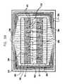
- the encapsulation 50surrounds the device substrate 350 on both sides, and comprises an epoxy resin matrix 363 .
- a plurality of particles 360are provided, of various sizes, shapes and/or magnetic permeabilities. These particles may be made out of Ni—Co—Fe alloy (i.e. a Ferrite alloy).
- a pair of plate-shaped permanent magnets 365 a , 365 bare provided above and below the encapsulation layers 50 , and bonded thereto by the epoxy resin 363 .
- the magnets 365 a , 365 bare arranged with their poles aligned in the same direction, which in this embodiment is conveniently perpendicular to the plates 365 .
- an outer casing 370 of soft magnetic core materialSurrounding the plates 365 and encapsulation 50 is an outer casing 370 of soft magnetic core material.
- the effect of the casing 370is to confine the magnetic field substantially within the casing, and to isolate it from external magnetic fields. It has a suitably high magnetic permeability (10 3 to 10 6 may be found suitable).
- the effect of the particles 360is to distort the magnetic field lines. Due to the non-uniformity of the distribution of the particles 360 , the field lines are irregular in shape.
- magnetic properties measured by the sensors 150will generally be different at each of the sensors, as described above.
- any attempt to remove the outer shield 370will itself change the distribution of the magnetic field and therefore make it impossible to read the key.
- the local variations in the (high) permeability of randomly distributed Ferromagnetic particlesis used to change the inductivity of crossing wires comprising the sensors 150 .
- FIG. 6shows structure of an embodiment in which local variations in the resistivity of the encapsulation are used to generate the key.
- the sensors 150comprise conductive openings in contact with the encapsulation 50 , and are individually connectable to a voltage supply line and to a ground line.
- one of the sensors 381is connected to a voltage supply line and another 383 to the earth line. The current passing through either of the sensors (provided through a current sensing resistor) provides the sensor output.
- the encapsulation 50surrounds the semiconductor substrate 350 of the device.
- a conductive powder having a relatively high electrical resistancesuch as graphite is intermixed.
- semiconductive materialssuch as Gallium, Copper Oxide or Selenium may be used.
- an outer conductive metal casing 390may be provided, bonded to the epoxy resin matrix 363 .
- the sensor output reading for each point in this casemay conveniently be calculated as the sum of the currents measured as flowing into each of it's neighbours from the sensor, so that a point on the substrate (and the encapsulation above it) will lie within the areas to which several sensors are responsive (i.e. the areas of the encapsulation sensed by neighbouring sensors overlap).
- temperature variationsmay cause resistivity fluctuations, so the difference between pairs of resistance measurements (each one being between a pair of the sensors) are taken at a subtract node, prior to digitisation. This reduces the temperature effect.
- the ratio, or any other differential measurementcould be used.
- This embodimenthas substantially the same structure as the last embodiment, except where differences are mentioned.
- an inner conductive layer 391 of, for example, aluminiumis provided, in electrical contact with the encapsulation 50 , and connected to the earth pin of the integrated circuit.
- each of the sensors 150is selectively connectable to a supply line, via a current sensing resistor.
- each one in turnis connected to the supply line, and the current through each flowing through the sensor and the encapsulation to the grounded metal layer 391 is measured through the current sensing resistor.
- resistances R 1 –R 5 from the sensors 392 , 394 , 396 , 398 , 400are successively measured in a scan. Again, differential measurements are preferred.
- FIGS. 8 a and 8 bshow an embodiment using capacitative sensors.
- each sensormerely comprises a contact pad below a layer 410 of insulating material, to block the passage of direct current, and a circuit for applying an alternating voltage and for measuring the current passing through the pad.
- a layer 405is grounded, as before.
- the layer 390may be an outer protective casing in this embodiment.
- a plurality of particles 411are provided within the resin 363 . The particles are such as to change the dielectric constants of the encapsulation 50 locally.
- a signal with a rapidly changing componenti.e. an alternating component
- a signal with a rapidly changing componentis applied through each sensor 150 by the analogue multiplexer.
- a signalmay be obtained by rapidly alternating the sensor 150 between 0 volts and supply voltage level, so as to produce a signal with an alternating component between the sensors 150 and the upper layer 390 (the direct current component will be blocked by the insulating layer 410 ).
- the current passing through the sensor(and hence a measure of the capacitance of the material above the sensor) is measured, for example using a current sensing resistor as described above.
- FIG. 9a structure of the key holding register will be described which is suitable to prevent attacks by freezing the key register using radiation or cooling.
- An input array of two to one multiplexers 602 a , 602 b , . . . 602 eeach receive one bit of the key at a first input port. In this case, there are 64 such two bit multiplexers.
- each of the multiplexers 602goes to the data input of a respective one of a bank of D type flip flops 604 a , 604 b , . . . 604 e .
- the normal (i.e. uninverted) output of each flip flop 604goes to a respective first input of one of a second bank of two to one multiplexers 606 a , 606 b , . . . 606 e.
- each bit of the keycan be clocked through the first multiplexer, the D type flip flop and the second multiplexer.
- each of the flip flops 604is connected to an OR gate 608 , which receives the reset line from the CPU 100 , and an input from a security fault detector (not shown).
- a security fault detectornot shown
- each flip flopis fed forward to the second input of the respective second multiplexer 606 and to the second input of the respective first multiplexer 602 .
- each of the D type flop flopsis fed from a further two way multiplexer 610 , a first port of which receives the CPU clock signal and a second port of which receives a random clock signal.
- a load/run linewhich changes states depending on whether the chip is arranged to load data or to execute the CPU program, selects which of the two input ports of each of the first multiplexer 602 is routed to its output port.
- a further flip flop 612has its reset line connected to the output of the OR gate 608 , its input connected to the output of the multiplexer 610 , and its output connected to the control input of the multiplexers 606 so as to select which of the two input ports is routed to the output thereof.
- the flip flop 612alternates between the genuine and inverted outputs of the bank of D type flip flops 604 each clock cycle.
- the effectis to toggle each bit of the key in the register of flip flops every (random) clock cycle, whilst maintaining the key on the output ports of the bank of second multiplexers for use in en/decryption.
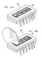
- FIG. 10shows an embodiment which permits the present invention to be used with separate integrated circuits.
- a separate CPU or microprocessor unit chip 470is provided, together with a separate non-volatile memory chip 460 .
- the memoryshould be writable, such as FLASH or EEPROM, as disclosed above.
- an integrated circuit 450connected to the address and data buses of the CPU 470 and the memory 460 , containing the security features of the present invention. All three are provided on a common printed circuit board 485 (shown in FIG. 11 ).
- the sensors 150 in this embodimentare distributed over the print circuit board 485 and connected via conductors to the integrated circuit 450 . They are provided on both sides of the printed circuit board 485 and also on the integrated circuit 450 .
- encapsulation 50Surrounding the PCB 485 at either side is encapsulation 50 containing features 385 which may be of any of the above types, suitable to be sensed by the sensors 150 .
- the encapsulation 50is provided around and pins are added to provide electrical contact. Finally, a protective shell 480 is added to protect the encapsulation 50 from accidental damage.
- the deviceperforms an initialisation operation in which the data is supplied to the device via the I/O interface, then encrypted in the key derived from the encapsulation 50 , and then stored into the memory 460 .
- circuit 450contains all of the components other than the memory 460 and CPU 470 described in the earlier embodiments.
- this embodimentenables the invention to be used with conventional or third party memory and CPU chip products without major modification thereof.
- FIGS. 12A to 12Cillustrate an embodiment in which the encapsulation 50 contains, in addition to a plurality of randomly distributed property-modifying particles as described in the above embodiments, a plurality of microcapsules containing one or more encapsulated substances (i.e. in liquid form).
- a plurality of microcapsules containing one or more encapsulated substancesi.e. in liquid form.
- capsules of first and second different substances 500 , 510may be provided, which will react together on contact to produce a chain reaction that will rupture further microcapsules.
- FIG. 12Bshows an attempt to mechanically open the chip encapsulation
- FIG. 12Cshows that, as a result, capsules 500 and 510 are ruptured and come into contact with each other, setting off a two part exothermic reaction which then ruptures further encapsulations and thus propagates through the encapsulation 50 . This produces a substantial alternation in the parameters measured by the sensors 150 , destroying the encryption key.
- the encapsulationshould be such that the encapsulated regions will not rupture due to normal handling but will rupture readily on attempts to piece or penetrate the packaging 50 . It is only necessary that the encapsulation should be substantially changed; it is not necessary that the underlying chip should also be destroyed.
- the encapsulation or packaging material 50is made of a light transmissive matrix 515 such as a polymer (e.g. epoxy, polyacryl), or alkali silicate (such as NaSi 4 ). It might alternatively comprise a crystalline light transmissive solid (e.g. a crystallised polymer).
- a light transmissive matrix 515such as a polymer (e.g. epoxy, polyacryl), or alkali silicate (such as NaSi 4 ). It might alternatively comprise a crystalline light transmissive solid (e.g. a crystallised polymer).
- At least one light source 520(shown in FIG. 13A as a plurality of light sources), positioned on the surface of the integrated circuit 350 .
- the light sourcesmay conveniently be light emitting diodes (LEDs).
- the array of sensors 150 in this embodimentare photosensors.
- the polymer encapsulation 515includes a plurality of randomly dispersed particles 530 which interact with the light emitted from the light sources 520 .
- the particlesmay refract, reflect, diffract or absorb light.
- the light from the sourcesthus produces on the array of sensors 150 an interference pattern which is characteristic of the distribution of the particles and is used to produce a cryptographic key as disclosed above.
- the particlesmay be for example may be small crystal grains.
- the matrixmay include a plurality of decrystallised areas to fulfil the role of the particles 530 .
- the decrystallised areasmay be produced in a known fashion using a focused laser beam.
- the encapsulation 50 of this embodimentis surrounded, preferably completely, by a bonded-on, hard outer covering 540 which is light reflective on the inside and does not allow the entry of light from the outside. Thus, the light sensed by the sensors 150 is unaffected by external light conditions.
- a multiplicity of light raysare emitted by the light sources 520 .
- Rays such as the ray 560 which reach an external surface of the encapsulation 50 and an internal surface of the outer covering 540are reflected back inwards, and will eventually reach one of the sensors (labelled 565 ).
- FIG. 13Bshows the effects of intrusively opening the apparatus. This creates an opening 570 , causing rays such as the ray 560 to pass out through the opening 570 rather than be internally reflected. Thus, the environment sensed by the sensor 565 has now changed, changing the key and thus rendering decryption impossible.
- each photosensoris paired with a light emitting diode, and the pairs are positioned around the periphery of the chip. Light from the diode of one pair is then sensed by the photosensors of the others.
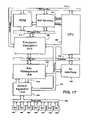
- the memory 110has been of an electrically alterable kind, to allow each integrated circuit after fabrication to sense the parameters of its encapsulation and thus derive its unique encryption key, and then to store data in the memory 110 using that key.
- This embodimentenables a read only memory (ROM), in which data has been stored prior to this initialisation operation, to be used.
- ROMread only memory
- this embodimentis the same as that of FIG. 1B , except for the presence of an additional memory 111 , and a difference in the operation of the encryption/decryption unit 120 .
- memory 110is a read only memory (ROM). Data is provided within the read only memory 110 in encrypted form, encrypted using a first predetermined encryption key. The first encryption key is then stored, in the clear, in the second memory 111 which is writeable, non-volatile, memory (e.g. Flash or EEPROM).
- ROMread only memory
- steps 1002 and 1004 of FIG. 14are performed on initialisation. Then, the value of the predetermined encryption key (i.e. the key needed to decrypt the contents of the memory 110 ) is read from the second memory, and encrypted using the second key, which was formed in step 1004 (i.e. that derived from the parameters of the encapsulation). The first key encrypted under the second is then written back into the second memory 111 in encrypted form.
- the predetermined encryption keyi.e. the key needed to decrypt the contents of the memory 110
- the second keywhich was formed in step 1004 (i.e. that derived from the parameters of the encapsulation).
- the first key encrypted under the secondis then written back into the second memory 111 in encrypted form.
- the first stepis to read the second memory 111 and decrypt the first key therefrom. After that, the operations of reading and writing data are substantially as described in the embodiments above.
- the clear text value of the first keyis erased from the register in which it is held, which is also toggled as in FIG. 9 to defeat a freeze attack.
- the key used to encrypt or decrypt the data held in the first (ROM) memory 110is not permanently latched or held in clear text form, so that it cannot be reading by stripping away the encapsulation.
- the first keymay be the same for a batch of ROMs, which may therefore be mask-programmed, leading to a cost saving. Only the key-encrypting key derived from the encapsulation need be stored in the second memory.
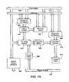
- FIGS. 17 and 18which broadly correspond to FIGS. 1B and 2 of the first embodiment, and to FIG. 19 .
- a ROM 110is used as storage. Additionally, in this embodiment, a processor having a byte-wide (i.e. 8 bit wide) data bus is used, with 64 bit block encryption as discussed above.
- the scanned values from the encapsulationare not directly used to form the key to decrypt the key for the ROM data; instead, they are combined with a second digital string, which will hereafter be referred to as the “pairing key”, whilst the string of scanned values will be referred to as the “shell key”.
- the pairing key nor the shell keyare keys in a strict sense, since they are not actually used to encrypt or decrypt data themselves, but the pairing key should be generated as if it were a key).
- the key used to decrypt datacannot be derived without the pairing key.
- FIG. 17there are provided a sensor acquisition (or scanning) unit 704 which scans the signals from the sensors 150 received via sensor bus 708 , and submits the digitally acquired signals 718 to a key management unit 702 , which forms the keys used for encryption or decryption.
- a sensor acquisition (or scanning) unit 704which scans the signals from the sensors 150 received via sensor bus 708 , and submits the digitally acquired signals 718 to a key management unit 702 , which forms the keys used for encryption or decryption.
- the KSU 704provides a standard interface to the KMU; that is to say, it includes all the necessary components for whichever types of sensors it is to be used with and converts their outputs to a standard digital form.
- any customisation of the apparatus of this embodiment for different sensor systemsis concentrated only in the sensors 150 and KSU 704 .
- Interconnecting the componentsare an address bus 712 ; a data bus 710 ; a control bus 706 ; a key management unit bus 716 ; an encrypted bus 714 ; and a key bus 720 .
- the control bus 706allows the CPU 100 to signal requests to the various other functional blocks (the KSU 704 , KMU 702 and the EDU 120 ).
- FIG. 18illustrates a portion of the apparatus of FIG. 17 comprising the EDU 120 . It shows in particular the relationship between the EDU 120 , the CPU 100 , the memory 110 and key holding registers.
- the EDU 120comprises a symmetric block encryption/decryption device (operable for example to perform a DES encryption and decryption operation); a pair of key holding registers 722 , 724 ; a column width (64 bit) dual port plaintext register 728 ; and a memory access control (MAC) circuit 726 (responsive to the address bus) which selects the appropriate one of the two keys held in the two key holding registers 722 , 724 and causes it to be supplied to the block encryption/decryption unit 260 .
- MACmemory access control
- each byte of the 64 bit register 728is a respective byte wide register 730 a – 730 h .
- the memory access control circuit 726is operable to select one of the byte registers 730 .
- the key management unit 702comprises a sensor address generator 801 , a shell key register 804 , a fingerprint register 808 , and a pairing key register 824 . It also comprises logic circuits performing a pairing function 822 and a fingerprint function 806 , and a comparison circuit 812 .
- the KMU 702stores a random number as the pairing key, in an erasable register (i.e. non-volatile memory) 824 .
- the random numberis unique to each device of a batch and is supplied through the I/O circuit on initialisation and stored in the register by the loader program.
- the second key register 724Within the second key register 724 is the key which was used to encrypt the data held in the ROM 110 , which is supplied through the I/O circuit on initialisation and stored initially in clear form in the register 724 .
- the CPUraises a signal on the control bus 706 to cause the KSU 704 to scan the encapsulation properties.
- the KSUthen receives measurement values 802 from the sensor units 150 over the sensor bus 708 , and transmits these to the key management unit (KMU) 702 . where they are stored in the (non-volatile, erasable) Shell Key Register 804 which, as in preceding embodiments, alternates the data to prevent a “freezing” attack.
- KMUkey management unit
- a “fingerprint” characterising the measurement valuesis calculated from the contents of the Shell Key Register 804 , by the fingerprint function circuit 806 ;
- the fingerprint functionis a function which combines the measurements in a manner which does not depend on their order and may conveniently be the sum of the measurements.
- the calculated fingerprintis stored in the (non-volatile, erasable) Fingerprint register 808 , where it will remain throughout use of the device (unless tampering is detected).
- the final key to be usedis calculated from the contents of the Shell Key Register 804 and the pairing key register 824 using, for example, an XOR combination operation and stored in the final key register 722 where it will remain until power is removed from the device, at which point it will be erased.
- this registeralternates the data to prevent a “freezing” attack. Where necessary, it will be accessed by the EDU over the KMU bus 716 .
- the key to the ROMwhich was initially stored in the clear in register 724 , is retrieved and encrypted under the final key from register 722 , and stored back in the register 724 in that encrypted form, where it will remain until power is removed from the device, at which point it will be erased.
- This registeralso alternates the data to prevent a “freezing” attack.
- the CPU 100causes the re-acquisition of the sensor values, performs a fingerprint check, recalculates the final key, and re-encrypts the ROM key.
- the acquisition unit 704scans the sensors 150 relatively frequently (at intervals shorter than the time taken to penetrate the encapsulation, for example every second).
- the sensor address generator 801calculates a different sequence of sensor readings before each new scan, so that the order of scanning is frequently varied. However, the scanned values themselves should be the same from in each scan, albeit presented in a different order.
- the KMU 704is arranged, after each scan of the sensor bus 708 , to compare the measured encapsulation properties with the fingerprint, by applying the fingerprint function 806 to the contents of the shell key register 804 and comparing the results with the contents of the fingerprint register 808 .
- the tamper detection circuit 812sends a signal to the CPU indicating an alarm condition, and the CPU sends an alarm signal on the control bus 706 to cause the KSU, KMU and EDU to erase the pairing key from the pairing key register 824 .
- the contents of the shell key register 804 , fingerprint register 808 and encryption key registers 722 , 724are also erased.
- the 64 bit column which includes the byte requested by the CPUis supplied in the (64 bit wide) encrypted bus 714 to the encryption/decryption circuit 260 . If the memory access control circuit 726 detects that the address lies within the address space of the writeable memory 111 , the first key register 722 is selected and used for data decryption; otherwise, if it lies within the address space of the read only memory 110 , the first key register 722 is selected and then the second key register 724 is selected and the final key is used to decrypt the ROM key which is then used for data decryption.
- the decrypted 64 bit wordis written by the block encryption unit 260 to the plaintext register 728 .
- the memory access control circuit 726selects the appropriate one of the registers 730 a–h which contains the byte requested by the CPU 100 and causes the selected register to load that byte onto the data bus 710 for reading by the CPU 100 .
- performing a write operationrequires a read operation first, as data is encrypted in larger blocks than those used by the CPU 100 . Accordingly, after the plain text of a column is available in the plaintext register 728 (following the read step as discussed above), the memory access control circuit 726 places the byte to be written by the CPU 100 from the data bus 710 into the appropriate one of the byte wide registers 730 a – 730 h and thence it is overwritten over the corresponding 8 bits within the plaintext register 728 .
- the block encryption circuit 260then encrypts the contents of the plaintext register 728 using the current key, and the column is written back to the non-volatile memory 111 on the encrypted bus 714 .
- this embodimentis best understood by comparison with the first embodiment. If, in the first embodiment, it were possible for a hacker to cut a small hole down to the CPU 100 , it might in principle then be possible to read out the sensor values. The drilling should have caused some change in properties locally, so that readings from a few sensors will have changed, but readings from many of the others may not have done so. It might then be possible for a hacker to mount a “brute force” attack by trying all values of the few changed bits.
- the permutation of the scan ordermeans that he will not know where, in the sequence of measurement readings which go to make up the key, the corrupted bits (which are to be subject to a “brute force” attack) should go, so that the task of mounting such an attack is increased by the permutation of scanning order.
- radiationis used as the sensed property.
- the epoxy resin of the encapsulation 50is mixed with a small amount of particles which transmit beta rays (e.g. particles of radioactive isotopes such as uranium).
- the beta rayswill arrive from all sides of the chip.
- the sensorsare beta detectors (which may be x-ray detectors) placed at many locations. The detectors will receive a complex pattern of beta rays generated by the chip case. As before, any attempt at penetration will change the key produced from the sensors radiation levels.
- the amount of radiation generatedwill be less than naturally occurring cosmic rays.
- the chipmay be surrounded with some radiation absorbing substance, such as a thin layer of lead, or a layer of epoxy mixed with Barium Sulphate.
- varying particles of ferroelectric materialsmay be provided in the matrix of the layer 50 , and an electric field applied across the layer 50 by plate electrodes.
- the fieldis modified locally by the particles, and this can be sensed by sensors similar to those used in the capacitative embodiment above.
- varying particles of magnetised ferromagnetic materialsmay be used to generate a set of local magnetic fields sensed by Hall effect sensors.
- spin valve transistors(which can be made on a very small scale) could be used.
- the keyis derived from the sum (or several sums) of sensor readings
- an attempt to remove the encapsulationwill definitely change the key value. If the effect of, for example, reducing the thickness of the encapsulation were to increase some readings and decrease others then the key might in principle remain unchanged, which would be undesirable.
- circuits shownare capable of both encryption and decryption, it would be possible in some applications merely to provide decryption within the device if data is only to be read from memory.
- circuits employedcould be based on Silicon, or on III–V materials such as Gallium Arsenide. Whilst electronic circuits are described above, application of the invention to optoelectronic circuits or optical circuits or other circuits (for example molecular computing circuits) is not excluded.
Landscapes
- Engineering & Computer Science (AREA)
- Computer Hardware Design (AREA)
- General Physics & Mathematics (AREA)
- Physics & Mathematics (AREA)
- Computer Security & Cryptography (AREA)
- Theoretical Computer Science (AREA)
- Microelectronics & Electronic Packaging (AREA)
- General Engineering & Computer Science (AREA)
- Power Engineering (AREA)
- Condensed Matter Physics & Semiconductors (AREA)
- Computer Networks & Wireless Communication (AREA)
- Signal Processing (AREA)
- Software Systems (AREA)
- Storage Device Security (AREA)
- Semiconductor Integrated Circuits (AREA)
Abstract
Description
Claims (36)
Priority Applications (1)
| Application Number | Priority Date | Filing Date | Title |
|---|---|---|---|
| US09/745,811US7005733B2 (en) | 1999-12-30 | 2000-12-26 | Anti tamper encapsulation for an integrated circuit |
Applications Claiming Priority (2)
| Application Number | Priority Date | Filing Date | Title |
|---|---|---|---|
| US17399499P | 1999-12-30 | 1999-12-30 | |
| US09/745,811US7005733B2 (en) | 1999-12-30 | 2000-12-26 | Anti tamper encapsulation for an integrated circuit |
Publications (2)
| Publication Number | Publication Date |
|---|---|
| US20010033012A1 US20010033012A1 (en) | 2001-10-25 |
| US7005733B2true US7005733B2 (en) | 2006-02-28 |
Family
ID=22634377
Family Applications (1)
| Application Number | Title | Priority Date | Filing Date |
|---|---|---|---|
| US09/745,811Expired - LifetimeUS7005733B2 (en) | 1999-12-30 | 2000-12-26 | Anti tamper encapsulation for an integrated circuit |
Country Status (8)
| Country | Link |
|---|---|
| US (1) | US7005733B2 (en) |
| EP (1) | EP1243027A1 (en) |
| JP (1) | JP2003519852A (en) |
| KR (1) | KR100687071B1 (en) |
| CN (1) | CN1433576A (en) |
| AU (1) | AU783858B2 (en) |
| CA (1) | CA2395656A1 (en) |
| WO (1) | WO2001050530A1 (en) |
Cited By (129)
| Publication number | Priority date | Publication date | Assignee | Title |
|---|---|---|---|---|
| US20020029345A1 (en)* | 2000-07-13 | 2002-03-07 | Yusuke Kawasaki | Processing apparatus and integrated circuit |
| US20020188857A1 (en)* | 2001-06-11 | 2002-12-12 | William Orlando | Protected storage of a datum in an integrated circuit |
| US20030023846A1 (en)* | 1999-07-08 | 2003-01-30 | Broadcom Corporation | Classification engine in a cryptography acceleration chip |
| US20030188187A1 (en)* | 2002-03-25 | 2003-10-02 | Nec Corporation | Obfuscated source program, source program conversion method and apparatus, and source conversion program |
| US20030204743A1 (en)* | 2002-04-16 | 2003-10-30 | Srinivas Devadas | Authentication of integrated circuits |
| US20040025040A1 (en)* | 2002-08-02 | 2004-02-05 | Fujitsu Limited | Memory device and encryption/decryption method |
| US20040114765A1 (en)* | 2001-04-04 | 2004-06-17 | Pierre-Yvan Liardet | Extraction of a private datum to authenticate an integrated circuit |
| US20040123120A1 (en)* | 2002-12-18 | 2004-06-24 | Broadcom Corporation | Cryptography accelerator input interface data handling |
| US20040123123A1 (en)* | 2002-12-18 | 2004-06-24 | Buer Mark L. | Methods and apparatus for accessing security association information in a cryptography accelerator |
| US20040128458A1 (en)* | 2001-05-17 | 2004-07-01 | Wolfgang Buhr | Method and device for protecting data transmission between a central processor and a memory |
| US20040146163A1 (en)* | 2002-10-28 | 2004-07-29 | Nokia Corporation | Device keys |
| US20040252575A1 (en)* | 2001-02-15 | 2004-12-16 | Tero Karkkainen | Method and arrangement for protecting information |
| US20050051351A1 (en)* | 2001-11-28 | 2005-03-10 | De Jongh Petra Elisabeth | Semiconductor device, card, system, and methods of initializing and checking the authenticity and the identify of the semiconductor device |
| US20050104161A1 (en)* | 2003-11-18 | 2005-05-19 | Matsushita Electric Industrial Co., Ltd. | Semiconductor wafer |
| US20060049941A1 (en)* | 2004-09-03 | 2006-03-09 | Hunter Steve B | Reusable tamper respondent enclosure |
| US20060059345A1 (en)* | 2004-09-10 | 2006-03-16 | International Business Machines Corporation | System and method for providing dynamically authorized access to functionality present on an integrated circuit chip |
| US20060081497A1 (en)* | 2002-12-18 | 2006-04-20 | Koninklijke Philips Electronics N.V. | Tamper-resistant packaging and approach |
| US20060133604A1 (en)* | 2004-12-21 | 2006-06-22 | Mark Buer | System and method for securing data from a remote input device |
| US20060209584A1 (en)* | 2004-11-12 | 2006-09-21 | Srinivas Devadas | Securely field configurable device |
| US20060230440A1 (en)* | 2005-04-08 | 2006-10-12 | Victor Chuan-Chen Wu | Encryption removable storage system |
| US20070053515A1 (en)* | 2005-08-18 | 2007-03-08 | Samsung Electronics Co., Ltd. | Semiconductor device using a read-only memory (ROM) scrambling/descrambling method, and a method of operating the same |
| US20070139989A1 (en)* | 2003-01-14 | 2007-06-21 | Koninklijke Philips Electronics N.V. | Tamper-resistant packaging and approach using magnetically-set data |
| US20070152840A1 (en)* | 2006-01-05 | 2007-07-05 | Honeywell International Inc. | Method and system to detect tampering using light detector |
| US20070152839A1 (en)* | 2006-01-05 | 2007-07-05 | Honeywell International Inc. | Method and system to detect tampering using light detector |
| US20070157682A1 (en)* | 2006-01-11 | 2007-07-12 | Honeywell International Inc. | Clamshell protective encasement |
| US20070186117A1 (en)* | 2003-09-25 | 2007-08-09 | Klein Dean A | Secure processor-based system and method |
| US20070221117A1 (en)* | 2006-03-23 | 2007-09-27 | Honeywell International Inc. | Active protection for closed systems |
| US20070250938A1 (en)* | 2006-01-24 | 2007-10-25 | Suh Gookwon E | Signal Generator Based Device Security |
| US20070279969A1 (en)* | 2006-06-02 | 2007-12-06 | Raytheon Company | Intrusion detection apparatus and method |
| US20080073491A1 (en)* | 2006-09-27 | 2008-03-27 | Honeywell International Inc. | Anti-tamper enclosure system |
| US20080117046A1 (en)* | 2005-11-02 | 2008-05-22 | Honeywell International Inc. | Intrusion detection using pseudo-random binary sequences |
| US20080134349A1 (en)* | 2006-11-30 | 2008-06-05 | Honeywell International Inc. | Card slot anti-tamper protection system |
| US20080132118A1 (en)* | 2006-11-30 | 2008-06-05 | Honeywell International Inc. | Secure connector with integrated tamper sensors |
| US20080129501A1 (en)* | 2006-11-30 | 2008-06-05 | Honeywell International Inc. | Secure chassis with integrated tamper detection sensor |
| US20080170698A1 (en)* | 2003-08-25 | 2008-07-17 | Brant Candelore | Apparatus and method for an iterative cryptographic block |
| US20080183787A1 (en)* | 2007-01-26 | 2008-07-31 | Zou Zhengxian | Method for manufacturing serial numbers for integrated circuits |
| US20080192240A1 (en)* | 2007-02-08 | 2008-08-14 | Honeywell International Inc. | Methods and systems for recognizing tamper events |
| US20080219441A1 (en)* | 2004-03-24 | 2008-09-11 | Karl Asperger | Arrangement Comprising an Integrated Circuit |
| US7434043B2 (en) | 2002-12-18 | 2008-10-07 | Broadcom Corporation | Cryptography accelerator data routing unit |
| US20080288785A1 (en)* | 2003-08-07 | 2008-11-20 | Rao G R Mohan | Data Security and Digital Rights Management System |
| US20080286944A1 (en)* | 2005-02-11 | 2008-11-20 | Michel Thill | Method to Manufacture a Silicon Wafer Electronic Component Protected Against the Attacks and Such a Component |
| US20090060182A1 (en)* | 2007-09-04 | 2009-03-05 | Thomas Killian | Apparatus and method for enhancing the protection of media content |
| US20090065591A1 (en)* | 2007-09-12 | 2009-03-12 | Seiko Epson Corporation | Smart-card chip arrangement |
| US20090083833A1 (en)* | 2007-09-19 | 2009-03-26 | Verayo, Inc. | Authentication with physical unclonable functions |
| US7568110B2 (en) | 2002-12-18 | 2009-07-28 | Broadcom Corporation | Cryptography accelerator interface decoupling from cryptography processing cores |
| US20090321734A1 (en)* | 2008-06-30 | 2009-12-31 | Texas Instruments Incorporated | Capacitor-based method for determining and characterizing scribe seal integrity and integrity loss |
| US20100031375A1 (en)* | 2008-07-29 | 2010-02-04 | International Business Machines Corporation | Signal Quality Monitoring to Defeat Microchip Exploitation |
| US20100031376A1 (en)* | 2008-07-29 | 2010-02-04 | International Business Machines Corporation | Continuity Check Monitoring for Microchip Exploitation Detection |
| US20100026337A1 (en)* | 2008-07-29 | 2010-02-04 | International Business Machines Corporation | Interdependent Microchip Functionality for Defeating Exploitation Attempts |
| US20100026313A1 (en)* | 2008-07-29 | 2010-02-04 | International Business Machines Corporation | Capacitance Structures for Defeating Microchip Tampering |
| US20100026336A1 (en)* | 2008-07-29 | 2010-02-04 | International Business Machines Corporation | False connection for defeating microchip exploitation |
| US20100026326A1 (en)* | 2008-07-29 | 2010-02-04 | International Business Machines Corporation | Resistance Sensing for Defeating Microchip Exploitation |
| US20100026506A1 (en)* | 2008-07-29 | 2010-02-04 | International Business Machines Corporation | Capacitance-Based Microchip Exploitation Detection |
| US20100025479A1 (en)* | 2008-07-29 | 2010-02-04 | International Business Machines Corporation | Doped Implant Monitoring for Microchip Tamper Detection |
| US20100078636A1 (en)* | 2007-02-20 | 2010-04-01 | Nxp, B.V. | Semiconductor device with backside tamper protection |
| US20100119062A1 (en)* | 2006-08-03 | 2010-05-13 | Wivenhoe Technology Limited | Device to generate a machine specific identification key |
| US20100146641A1 (en)* | 2003-02-20 | 2010-06-10 | Nxp B.V. | Method and device for protection of an mram device against tampering |
| US20100181999A1 (en)* | 2007-10-09 | 2010-07-22 | Nds Limited | Tamper-detecting electronic system |
| US20100213590A1 (en)* | 2009-02-25 | 2010-08-26 | Conexant Systems, Inc. | Systems and Methods of Tamper Proof Packaging of a Semiconductor Device |
| WO2010104543A3 (en)* | 2008-12-31 | 2010-12-02 | Arizona Board Of Regents, For And On Behalf Of Arizona State University | Integrated circuits secure from invasion and methods of manufacturing the same |
| US20110099117A1 (en)* | 2008-06-27 | 2011-04-28 | Koninklijke Philips Electronics N.V. | Device, system and method for verifying the authenticity integrity and/or physical condition of an item |
| US20110113256A1 (en)* | 2009-11-12 | 2011-05-12 | Stmicroelectronics (Rousset) Sas | Secure Method for Processing a Content Stored Within a Component, and Corresponding Component |
| US8213207B2 (en) | 2010-08-25 | 2012-07-03 | Honeywell International Inc. | Printed board assembly movement detection |
| US8275996B1 (en) | 2010-04-12 | 2012-09-25 | Stephen Waller Melvin | Incremental encryption of stored information |
| US8429420B1 (en) | 2010-04-12 | 2013-04-23 | Stephen Waller Melvin | Time-based key management for encrypted information |
| US8675868B1 (en)* | 2008-07-01 | 2014-03-18 | Maxim Integrated Products, Inc. | Encrypting an address-dependent value along with code to prevent execution or use of moved code |
| US8752210B2 (en) | 2012-01-10 | 2014-06-10 | International Business Machines Corporation | Implementing data theft prevention |
| US8797059B2 (en) | 2012-03-01 | 2014-08-05 | International Business Machines Corporation | Implementing carbon nanotube based sensors for cryptographic applications |
| US8812875B1 (en) | 2010-04-12 | 2014-08-19 | Stephen Melvin | Virtual self-destruction of stored information |
| US8811072B2 (en) | 2012-03-13 | 2014-08-19 | Honeywell International Inc. | Magnetoresistive random access memory (MRAM) package including a multilayer magnetic security structure |
| US8819842B2 (en)* | 2012-11-20 | 2014-08-26 | International Business Machines Corporation | Implementing conductive microcapsule rupture to generate a tamper event for data theft prevention |
| WO2014132114A1 (en)* | 2013-03-01 | 2014-09-04 | Marvell World Trade Ltd. | Anti-tamper system based on dual random bits generators for integrated circuits |
| US8854870B2 (en) | 2012-03-13 | 2014-10-07 | Honeywell International Inc. | Magnetoresistive random access memory (MRAM) die including an integrated magnetic security structure |
| US9245202B2 (en) | 2013-06-06 | 2016-01-26 | International Business Machines Corporation | Tamper detection with microcaspule rupture |
| US9264426B2 (en) | 2004-12-20 | 2016-02-16 | Broadcom Corporation | System and method for authentication via a proximate device |
| US9342710B2 (en) | 2013-11-21 | 2016-05-17 | Nxp B.V. | Electronic tamper detection |
| US20160174388A1 (en)* | 2014-12-15 | 2016-06-16 | International Business Machines Corporation | Printed circuit board security using embedded photodetector circuit |
| US20160255058A1 (en)* | 2012-07-13 | 2016-09-01 | Angel Secure Networks, Inc. | System and method for policy driven protection of remote computing environments |
| US9554477B1 (en) | 2015-12-18 | 2017-01-24 | International Business Machines Corporation | Tamper-respondent assemblies with enclosure-to-board protection |
| US9555606B1 (en) | 2015-12-09 | 2017-01-31 | International Business Machines Corporation | Applying pressure to adhesive using CTE mismatch between components |
| US9560737B2 (en) | 2015-03-04 | 2017-01-31 | International Business Machines Corporation | Electronic package with heat transfer element(s) |
| US9565021B1 (en) | 2015-11-16 | 2017-02-07 | International Business Machines Corporation | Shape actuation encapsulant of a cryptographic module |
| US9578764B1 (en) | 2015-09-25 | 2017-02-21 | International Business Machines Corporation | Enclosure with inner tamper-respondent sensor(s) and physical security element(s) |
| US9591776B1 (en) | 2015-09-25 | 2017-03-07 | International Business Machines Corporation | Enclosure with inner tamper-respondent sensor(s) |
| US9818871B1 (en) | 2016-10-20 | 2017-11-14 | Cisco Technology, Inc. | Defense layer against semiconductor device thinning |
| US9858776B1 (en) | 2016-06-28 | 2018-01-02 | International Business Machines Corporation | Tamper-respondent assembly with nonlinearity monitoring |
| US9859226B1 (en) | 2016-12-13 | 2018-01-02 | International Business Machines Corporation | Core-shell particles for anti-tampering applications |
| US9881880B2 (en) | 2016-05-13 | 2018-01-30 | International Business Machines Corporation | Tamper-proof electronic packages with stressed glass component substrate(s) |
| US9894749B2 (en) | 2015-09-25 | 2018-02-13 | International Business Machines Corporation | Tamper-respondent assemblies with bond protection |
| US9904811B2 (en) | 2016-04-27 | 2018-02-27 | International Business Machines Corporation | Tamper-proof electronic packages with two-phase dielectric fluid |
| US9913370B2 (en) | 2016-05-13 | 2018-03-06 | International Business Machines Corporation | Tamper-proof electronic packages formed with stressed glass |
| US9913389B2 (en) | 2015-12-01 | 2018-03-06 | International Business Corporation Corporation | Tamper-respondent assembly with vent structure |
| US9911012B2 (en) | 2015-09-25 | 2018-03-06 | International Business Machines Corporation | Overlapping, discrete tamper-respondent sensors |
| US9916744B2 (en) | 2016-02-25 | 2018-03-13 | International Business Machines Corporation | Multi-layer stack with embedded tamper-detect protection |
| US9924591B2 (en) | 2015-09-25 | 2018-03-20 | International Business Machines Corporation | Tamper-respondent assemblies |
| US9978231B2 (en) | 2015-10-21 | 2018-05-22 | International Business Machines Corporation | Tamper-respondent assembly with protective wrap(s) over tamper-respondent sensor(s) |
| US9999124B2 (en) | 2016-11-02 | 2018-06-12 | International Business Machines Corporation | Tamper-respondent assemblies with trace regions of increased susceptibility to breaking |
| US20180165558A1 (en)* | 2016-12-09 | 2018-06-14 | Lexmark International, Inc. | Magnetic Keys Having a Plurality of Magnet Layers with Holes |
| US10007811B2 (en) | 2015-02-25 | 2018-06-26 | Private Machines Inc. | Anti-tamper system |
| US10098235B2 (en) | 2015-09-25 | 2018-10-09 | International Business Machines Corporation | Tamper-respondent assemblies with region(s) of increased susceptibility to damage |
| US10136519B2 (en) | 2015-10-19 | 2018-11-20 | International Business Machines Corporation | Circuit layouts of tamper-respondent sensors |
| US20180340850A1 (en)* | 2017-05-24 | 2018-11-29 | International Business Machines Corporation | Chemiluminescence for tamper event detection |
| US10168185B2 (en) | 2015-09-25 | 2019-01-01 | International Business Machines Corporation | Circuit boards and electronic packages with embedded tamper-respondent sensor |
| US10172239B2 (en) | 2015-09-25 | 2019-01-01 | International Business Machines Corporation | Tamper-respondent sensors with formed flexible layer(s) |
| US10171498B2 (en) | 2016-02-19 | 2019-01-01 | International Business Machines Corporation | Secure crypto module including electrical shorting security layers |
| WO2019006090A1 (en) | 2017-06-28 | 2019-01-03 | Tetramer Technologies, Llc | Frangible security device |
| US10212300B2 (en) | 2016-12-09 | 2019-02-19 | Lexmark International, Inc. | Magnetic keys having a plurality of magnetic plates |
| US10229352B2 (en) | 2013-11-22 | 2019-03-12 | Infineon Technologies Ag | Chip arrangement and method for checking whether a chip is arranged in an intended chip carrier |
| US10271424B2 (en) | 2016-09-26 | 2019-04-23 | International Business Machines Corporation | Tamper-respondent assemblies with in situ vent structure(s) |
| US10299372B2 (en) | 2016-09-26 | 2019-05-21 | International Business Machines Corporation | Vented tamper-respondent assemblies |
| US10306753B1 (en) | 2018-02-22 | 2019-05-28 | International Business Machines Corporation | Enclosure-to-board interface with tamper-detect circuit(s) |
| US10321589B2 (en) | 2016-09-19 | 2019-06-11 | International Business Machines Corporation | Tamper-respondent assembly with sensor connection adapter |
| US10327343B2 (en) | 2015-12-09 | 2019-06-18 | International Business Machines Corporation | Applying pressure to adhesive using CTE mismatch between components |
| US10327329B2 (en) | 2017-02-13 | 2019-06-18 | International Business Machines Corporation | Tamper-respondent assembly with flexible tamper-detect sensor(s) overlying in-situ-formed tamper-detect sensor |
| US10426037B2 (en) | 2015-07-15 | 2019-09-24 | International Business Machines Corporation | Circuitized structure with 3-dimensional configuration |
| US10566296B2 (en) | 2017-11-09 | 2020-02-18 | Lexmark International, Inc. | Physical unclonable functions in bank cards or identification cards for security |
| US10621351B2 (en) | 2016-11-01 | 2020-04-14 | Raptor Engineering, LLC. | Systems and methods for tamper-resistant verification of firmware with a trusted platform module |
| US10696899B2 (en) | 2017-05-09 | 2020-06-30 | International Business Machines Corporation | Light emitting shell in multi-compartment microcapsules |
| US10696761B2 (en) | 2017-06-23 | 2020-06-30 | International Business Machines Corporation | Light generating microcapsules for self-healing polymer applications |
| US10877398B2 (en) | 2016-08-03 | 2020-12-29 | Lexmark International, Inc. | Toner cartridge for image forming device including flight with magnetic particles to generate a magnetic field |
| US10926485B2 (en) | 2017-05-24 | 2021-02-23 | International Business Machines Corporation | Light generating microcapsules for photo-curing |
| US11122682B2 (en) | 2018-04-04 | 2021-09-14 | International Business Machines Corporation | Tamper-respondent sensors with liquid crystal polymer layers |
| US11139256B2 (en) | 2019-08-21 | 2021-10-05 | Micron Technology, Inc. | Tamper-resistant integrated circuits, and related methods |
| US11301593B2 (en)* | 2018-04-06 | 2022-04-12 | Fraunhofer-Gesellschaft Zur Foerderung Der Angewandten Forschung E.V. | PUF-film and method for producing the same |
| US11356287B2 (en) | 2015-10-09 | 2022-06-07 | Lexmark International, Inc. | Injection-molded physical unclonable function |
| US11411748B2 (en) | 2018-04-06 | 2022-08-09 | Fraunhofer-Gesellschaft Zur Foerderung Der Angewandten Forschung E.V. | PUF-film and method for producing the same |
| EP4086950A1 (en) | 2021-05-06 | 2022-11-09 | IHP GmbH - Innovations for High Performance Microelectronics / Leibniz-Institut für innovative Mikroelektronik | Semiconductor device with back side protection mechanism |
| WO2022233720A1 (en) | 2021-05-06 | 2022-11-10 | Ihp Gmbh - Innovations For High Performance Microelectronics / Leibniz-Institut Für Innovative Mikroelektronik | Semiconductor device with back side protection mechanism |
| US11586780B2 (en) | 2018-04-06 | 2023-02-21 | Fraunhofer-Gesellschaft Zur Foerderung Der Angewandten Forschung E.V. | PUF-film and method for producing the same |
Families Citing this family (122)
| Publication number | Priority date | Publication date | Assignee | Title |
|---|---|---|---|---|
| WO2001059544A2 (en)* | 2000-02-14 | 2001-08-16 | Rainbow Technologies B.V., Netherlands | Security module system, apparatus and process |
| DE10040188A1 (en)* | 2000-08-17 | 2002-02-28 | Infineon Technologies Ag | Seal for the authentication of sealed objects and methods for producing and testing the seal |
| US6901343B2 (en)* | 2001-01-10 | 2005-05-31 | Matsushita Electric Industrial Co., Ltd. | Multilayer board in which wiring of signal line that requires tamper-resistance is covered by component or foil, design apparatus, method, and program for the multilayer board, and medium recording the program |
| US7266703B2 (en)* | 2001-06-13 | 2007-09-04 | Itt Manufacturing Enterprises, Inc. | Single-pass cryptographic processor and method |
| JP2003051819A (en)* | 2001-08-08 | 2003-02-21 | Toshiba Corp | Microprocessor |
| WO2003046802A2 (en)* | 2001-11-28 | 2003-06-05 | Koninklijke Philips Electronics N.V. | Semiconductor device, card, methods of initializing, checking the authenticity and the identity thereof |
| EP1391853A1 (en)* | 2001-11-30 | 2004-02-25 | STMicroelectronics S.A. | Diversification of the unique identifier of an integrated circuit |
| KR100445406B1 (en)* | 2001-11-30 | 2004-08-25 | 주식회사 하이닉스반도체 | Apparatus for encrypting the data and method therefor |
| DE10162307A1 (en)* | 2001-12-19 | 2003-07-03 | Philips Intellectual Property | Production of mask-programmed ROMs, using a mask containing several systems, whereby encryption using the mask is carried out so that the produced systems have different keys |
| GB0202431D0 (en)* | 2002-02-02 | 2002-03-20 | F Secure Oyj | Method and apparatus for encrypting data |
| DE60331427D1 (en)* | 2002-04-09 | 2010-04-08 | Nxp Bv | METHOD AND ARRANGEMENT FOR PROTECTING A CHIIP AND VERIFYING ITS AUTHENTICITY |
| DE10223176B3 (en)* | 2002-05-24 | 2004-01-22 | Infineon Technologies Ag | Integrated circuit with safety-critical circuit components |
| JP4282951B2 (en)* | 2002-05-31 | 2009-06-24 | パイオニア株式会社 | SEMICONDUCTOR STORAGE ELEMENT, LIFE OPERATION STARTING DEVICE, AND INFORMATION RECORDING MEDIUM HAVING THE SEMICONDUCTOR STORAGE ELEMENT |
| IL165468A0 (en) | 2002-06-04 | 2006-01-15 | Nds Ltd | Prevention of tampering in electronic devices |
| JP2004023351A (en)* | 2002-06-14 | 2004-01-22 | Oki Electric Ind Co Ltd | Method for securing program of microcomputer |
| US7853788B2 (en)* | 2002-10-08 | 2010-12-14 | Koolspan, Inc. | Localized network authentication and security using tamper-resistant keys |
| US7200758B2 (en)* | 2002-10-09 | 2007-04-03 | Intel Corporation | Encapsulation of a TCPA trusted platform module functionality within a server management coprocessor subsystem |
| DE10247485A1 (en)* | 2002-10-11 | 2004-04-22 | Infineon Technologies Ag | Chip with attack protection, e.g. for chip card, has device for monitoring protective layer structure to detect external attacks, inhibit/interrupt data extraction, feed or handling if attack occurs |
| US7712147B2 (en)* | 2002-12-18 | 2010-05-04 | Nxp B.V. | Method and device for protection of an mram device against tampering |
| EP1576615B1 (en)* | 2002-12-18 | 2011-07-06 | Nxp B.V. | Hardware security device for magnetic memory cells |
| CN1729541A (en) | 2002-12-18 | 2006-02-01 | 皇家飞利浦电子股份有限公司 | Tamper-resistant packaging and approach |
| US8210120B2 (en)* | 2003-01-10 | 2012-07-03 | Microsemi Corporation | Systems and methods for building tamper resistant coatings |
| US7758911B2 (en)* | 2003-05-08 | 2010-07-20 | Honeywell International Inc. | Microelectronic security coatings |
| FR2859805B1 (en) | 2003-09-12 | 2006-06-02 | Arjo Wiggins Secutity Sas | SECURE PAPER COMPRISING A FIBROUS LAYER AND AN ELECTRONIC CHIP INTEGRATED WITH THIS FIBROUS LAYER |
| GB0410975D0 (en) | 2004-05-17 | 2004-06-16 | Nds Ltd | Chip shielding system and method |
| JP2008500601A (en)* | 2004-05-25 | 2008-01-10 | 松下電器産業株式会社 | Semiconductor memory card |
| EP1617472A1 (en)* | 2004-07-16 | 2006-01-18 | Axalto SA | An active protection device for protecting a circuit against mechanical and electromagnetic attack |
| US7202782B2 (en)* | 2004-08-04 | 2007-04-10 | Agere Systems Inc. | Method and apparatus for disabling an integrated circuit (IC) when an attempt is made to bypass security on the IC |
| US7343496B1 (en) | 2004-08-13 | 2008-03-11 | Zilog, Inc. | Secure transaction microcontroller with secure boot loader |
| US8074082B2 (en)* | 2004-10-08 | 2011-12-06 | Aprolase Development Co., Llc | Anti-tamper module |
| EP1817746A1 (en)* | 2004-10-18 | 2007-08-15 | Koninklijke Philips Electronics N.V. | Secure sensor chip |
| DE102005024379A1 (en)* | 2005-05-27 | 2006-11-30 | Universität Mannheim | A method for generating and / or embossing a recoverable cryptographic key in the production of a topographical structure |
| WO2006129738A1 (en)* | 2005-05-30 | 2006-12-07 | Semiconductor Energy Laboratory Co., Ltd. | Semiconductor device and method for operating the same |
| US11011396B2 (en) | 2013-01-05 | 2021-05-18 | Frederick A. Flitsch | Customized smart devices and touchscreen devices and cleanspace manufacturing methods to make them |
| US11024527B2 (en) | 2005-06-18 | 2021-06-01 | Frederick A. Flitsch | Methods and apparatus for novel fabricators with Cleanspace |
| FR2893436B1 (en)* | 2005-11-15 | 2008-02-15 | Oberthur Card Syst Sa | SECURING BETWEEN ELECTRONIC COMPONENTS OF A PORTABLE SECURE ELECTRONIC ENTITY |
| KR101194838B1 (en)* | 2006-01-20 | 2012-10-25 | 삼성전자주식회사 | High security mask ROM and data scramble/descramble method thereof |
| WO2007086046A2 (en)* | 2006-01-24 | 2007-08-02 | Nds Limited | Chip attack protection |
| US20070247182A1 (en)* | 2006-03-31 | 2007-10-25 | Beatty Timothy S | Protection of security key information |
| WO2007116355A2 (en)* | 2006-04-11 | 2007-10-18 | Koninklijke Philips Electronics N.V. | Challenge-response authentication of token by means physical uncloneable function |
| US7468664B2 (en)* | 2006-04-20 | 2008-12-23 | Nve Corporation | Enclosure tamper detection and protection |
| US8617913B2 (en) | 2006-08-23 | 2013-12-31 | Rockwell Collins, Inc. | Alkali silicate glass based coating and method for applying |
| US8581108B1 (en) | 2006-08-23 | 2013-11-12 | Rockwell Collins, Inc. | Method for providing near-hermetically coated integrated circuit assemblies |
| US8076185B1 (en)* | 2006-08-23 | 2011-12-13 | Rockwell Collins, Inc. | Integrated circuit protection and ruggedization coatings and methods |
| US7915527B1 (en) | 2006-08-23 | 2011-03-29 | Rockwell Collins, Inc. | Hermetic seal and hermetic connector reinforcement and repair with low temperature glass coatings |
| US8769275B2 (en)* | 2006-10-17 | 2014-07-01 | Verifone, Inc. | Batch settlement transactions system and method |
| JP4993143B2 (en)* | 2006-11-24 | 2012-08-08 | 日本電気株式会社 | MRAM |
| US8117445B2 (en)* | 2006-12-20 | 2012-02-14 | Spansion Llc | Near field communication, security and non-volatile memory integrated sub-system for embedded portable applications |
| WO2008099348A2 (en)* | 2007-02-16 | 2008-08-21 | Nxp B.V. | Semiconductor device identifier generation |
| EP2135254B1 (en) | 2007-03-09 | 2016-05-25 | NVE Corporation | Stressed magnetoresistive tamper detection devices |
| US7710286B1 (en) | 2007-03-30 | 2010-05-04 | Maxim Integrated Products, Inc. | Intrusion detection using a conductive material |
| US7868441B2 (en)* | 2007-04-13 | 2011-01-11 | Maxim Integrated Products, Inc. | Package on-package secure module having BGA mesh cap |
| US7923830B2 (en)* | 2007-04-13 | 2011-04-12 | Maxim Integrated Products, Inc. | Package-on-package secure module having anti-tamper mesh in the substrate of the upper package |
| US8681996B2 (en)* | 2007-07-31 | 2014-03-25 | Lsi Corporation | Asymmetric key wrapping using a symmetric cipher |
| EP2232412B1 (en)* | 2007-08-02 | 2019-03-06 | Nxp B.V. | Tamper-resistant semiconductor device and methods of manufacturing thereof |
| US7615416B1 (en) | 2007-08-31 | 2009-11-10 | Maxim Integrated Products, Inc. | Secure package with anti-tamper peripheral guard ring |
| US7898090B1 (en) | 2007-09-28 | 2011-03-01 | Ixys Ch Gmbh | General purpose ball grid array security cap |
| US8657191B2 (en) | 2007-10-18 | 2014-02-25 | Nxp B.V. | Magnetic detection of back-side layer |
| DE102007051788A1 (en) | 2007-10-30 | 2009-05-14 | Giesecke & Devrient Gmbh | Semiconductor chip with a protective layer and method for operating a semiconductor chip |
| US8443458B2 (en) | 2008-01-16 | 2013-05-14 | Telefonaktiebolaget Lm Ericsson (Publ) | Method and device for detecting the opening of a cover enclosing the device |
| US8552566B1 (en) | 2008-05-30 | 2013-10-08 | Maxim Integrated Products, Inc. | Integrated circuit package having surface-mount blocking elements |
| US20100123469A1 (en)* | 2008-11-19 | 2010-05-20 | Edward Craig Hyatt | System and method for protecting circuit boards |
| TWI498827B (en)* | 2008-11-21 | 2015-09-01 | Verayo Inc | Non-networked rfid-puf authentication |
| FR2940485B1 (en)* | 2008-12-24 | 2011-03-25 | Oberthur Technologies | METHOD FOR STORING DATA IN AN ELECTRONIC ENTITY AND ELECTRONIC ENTITY THEREFOR |
| US8811615B2 (en)* | 2009-08-05 | 2014-08-19 | Verayo, Inc. | Index-based coding with a pseudo-random source |
| US8468186B2 (en)* | 2009-08-05 | 2013-06-18 | Verayo, Inc. | Combination of values from a pseudo-random source |
| WO2012122994A1 (en)* | 2011-03-11 | 2012-09-20 | Kreft Heinz | Off-line transfer of electronic tokens between peer-devices |
| EP2512061A1 (en)* | 2011-04-15 | 2012-10-17 | Hanscan IP B.V. | System for conducting remote biometric operations |
| US9417894B1 (en) | 2011-06-15 | 2016-08-16 | Ryft Systems, Inc. | Methods and apparatus for a tablet computer system incorporating a reprogrammable circuit module |
| US10678951B2 (en)* | 2011-10-24 | 2020-06-09 | Maxim Integrated Products, Inc. | Tamper detection countermeasures to deter physical attack on a security ASIC |
| CN102521532A (en)* | 2011-11-30 | 2012-06-27 | 深圳市同方多媒体科技有限公司 | Protection method for digital copyright based on encryption chip |
| KR20140129207A (en)* | 2012-02-21 | 2014-11-06 | 마이크로칩 테크놀로지 인코포레이티드 | Cryptographic transmission system using key encryption key |
| US8909942B1 (en)* | 2012-03-30 | 2014-12-09 | Western Digital Technologies, Inc. | MRAM-based security for data storage systems |
| EP2665094A1 (en)* | 2012-05-15 | 2013-11-20 | Nxp B.V. | Tamper resistant IC |
| US9436940B2 (en)* | 2012-07-09 | 2016-09-06 | Maxim Integrated Products, Inc. | Embedded secure element for authentication, storage and transaction within a mobile terminal |
| GB2507954B (en)* | 2012-10-13 | 2018-07-04 | Korala Associates Ltd | A user terminal system and method |
| CN103605933A (en)* | 2012-12-13 | 2014-02-26 | 深圳市证通电子股份有限公司 | Key information storing method and device based on standard unit technology |
| US11462437B2 (en) | 2013-01-05 | 2022-10-04 | Frederick A. Flitsch | Customized smart devices and touchscreen devices and cleanspace manufacturing methods to make them |
| US12189828B2 (en) | 2013-01-05 | 2025-01-07 | Frederick A. Flitsch | Customized smart devices and touchscreen devices and cleanspace manufacturing methods to make them |
| US9507968B2 (en) | 2013-03-15 | 2016-11-29 | Cirque Corporation | Flying sense electrodes for creating a secure cage for integrated circuits and pathways |
| JP6126425B2 (en)* | 2013-03-27 | 2017-05-10 | 株式会社日立ハイテクサイエンス | Focused ion beam apparatus and control method thereof |
| DE102013205729A1 (en) | 2013-03-28 | 2014-10-02 | Fraunhofer-Gesellschaft zur Förderung der angewandten Forschung e.V. | Device and method with a carrier with circuit structures |
| DE102013014587B4 (en)* | 2013-08-29 | 2017-10-19 | Fachhochschule Schmalkalden | Method for IT protection of security-relevant data and its processing |
| WO2015061673A1 (en)* | 2013-10-25 | 2015-04-30 | Roximity, Inc. | Beacon security |
| DE202013011130U1 (en) | 2013-12-11 | 2014-01-10 | Giesecke & Devrient Gmbh | chip system |
| US9729320B2 (en)* | 2014-02-25 | 2017-08-08 | Cavium, Inc. | Apparatus and method for software enabled access to protected hardware resources |
| US9747967B2 (en) | 2014-09-26 | 2017-08-29 | Intel Corporation | Magnetic field-assisted memory operation |
| CN107077569B (en)* | 2014-10-20 | 2021-05-07 | 基岩自动化平台公司 | Tamper-resistant module for industrial control systems |
| DE102014016644A1 (en)* | 2014-11-11 | 2016-05-12 | Giesecke & Devrient Gmbh | Method for protection against unauthorized access |
| WO2016099644A1 (en)* | 2014-12-19 | 2016-06-23 | Private Machines Inc. | Systems and methods for using extended hardware security modules |
| US20160188495A1 (en)* | 2014-12-26 | 2016-06-30 | Intel Corporation | Event triggered erasure for data security |
| US10325131B2 (en)* | 2015-06-30 | 2019-06-18 | Synaptics Incorporated | Active matrix capacitive fingerprint sensor for display integration based on charge sensing by a 2-TFT pixel architecture |
| EP3147830B1 (en) | 2015-09-23 | 2020-11-18 | Nxp B.V. | Protecting an integrated circuit |
| US10410779B2 (en) | 2015-10-09 | 2019-09-10 | Lexmark International, Inc. | Methods of making physical unclonable functions having magnetic and non-magnetic particles |
| JP6690238B2 (en) | 2015-12-28 | 2020-04-28 | 富士通株式会社 | Electronic circuit and latch circuit for external action detection |
| DE102016109960A1 (en)* | 2016-05-31 | 2017-11-30 | Infineon Technologies Ag | Semiconductor package, smart card and method of manufacturing a semiconductor package |
| IT201600072154A1 (en)* | 2016-07-11 | 2018-01-11 | Ibm | ELECTRONIC DEVICES WITH INDIVIDUAL SAFETY CIRCUITS |
| US10395064B2 (en)* | 2016-09-02 | 2019-08-27 | Frederick A. Flitsch | Customized smart devices and touchscreen devices and clean space manufacturing methods to make them |
| GB2560716B (en)* | 2017-03-20 | 2022-05-25 | Blueskytec Ltd | Electronic anti-tamper device |
| EP3682471B1 (en)* | 2017-09-15 | 2023-11-08 | Cryptography Research, Inc. | Packaging techniques for backside mesh connectivity |
| DE102017009315B4 (en) | 2017-10-06 | 2019-11-21 | Sergej Gertje | Protection of automation programs against reverse development |
| US10381315B2 (en) | 2017-11-16 | 2019-08-13 | Samsung Electronics Co., Ltd. | Method and system for providing a reverse-engineering resistant hardware embedded security module |
| WO2019110998A1 (en) | 2017-12-07 | 2019-06-13 | Bae Systems Plc | Integrity monitor |
| DE102018209579B9 (en) | 2018-06-14 | 2024-03-14 | Infineon Technologies Ag | ELECTRONIC DEVICE AND METHOD FOR MAKING THE SAME |
| GB2577280B (en) | 2018-09-19 | 2022-11-09 | Blueskytec Ltd | Electronic anti-tamper device |
| CN112005249A (en)* | 2019-03-05 | 2020-11-27 | 华为技术有限公司 | Circuit for bare chip protection, bare chip and integrated circuit |
| CN111783171A (en)* | 2019-04-04 | 2020-10-16 | 利盟国际有限公司 | Physically Unclonable Functions for Security in Integrated Circuit Chip Packages |
| EP3761556A1 (en)* | 2019-07-04 | 2021-01-06 | Basf Se | New method for pseudo-random number generation for information encryption |
| CN110289244B (en)* | 2019-07-23 | 2024-07-30 | 南方电网科学研究院有限责任公司 | A cryptographic chip for preventing intrusive attacks on sensitive information |
| US11797718B2 (en) | 2019-08-23 | 2023-10-24 | Cryptography Research, Inc. | Anti-tamper shield based on strings of series resistors |
| FR3111737B1 (en)* | 2020-06-19 | 2022-07-08 | Commissariat Energie Atomique | CHIP OR BOX-SYSTEM PROTECTION USING THE GMI EFFECT |
| EP3941168A1 (en)* | 2020-07-14 | 2022-01-19 | ZKW Group GmbH | Vehicle module with a manipulation-detecting electronic control unit |
| US11437329B2 (en) | 2020-10-14 | 2022-09-06 | Globalfoundries U.S. Inc. | Anti-tamper x-ray blocking package |
| DE102021200770A1 (en)* | 2021-01-28 | 2022-07-28 | Continental Automotive Gmbh | ARRANGEMENT HAVING A MULTI-LAYER CIRCUIT BOARD AND METHODS OF OPERATING A MULTI-LAYER CIRCUIT BOARD |
| DE102021110607A1 (en)* | 2021-04-26 | 2022-10-27 | Semikron Elektronik Gmbh & Co. Kg | Device with functional component and plastic housing element and method for verifying the authenticity of such a device |
| US12204144B2 (en) | 2021-11-12 | 2025-01-21 | Globalfoundries U.S. Inc. | Bragg reflector for photonic chip security structure |
| US11815717B2 (en) | 2021-11-12 | 2023-11-14 | Globalfoundries U.S. Inc. | Photonic chip security structure |
| US20230214493A1 (en)* | 2021-12-30 | 2023-07-06 | Moxa Inc. | Computer System for Failing a Secure Boot in a Case Tampering Event |
| CN115393911B (en)* | 2022-08-19 | 2025-08-22 | 北京集创北方科技股份有限公司 | Fingerprint information encryption circuit, display device, electronic device and driver chip |
| DE102023102691A1 (en)* | 2023-02-03 | 2024-08-08 | btv technologies gmbh | Method for writing data to an IC and system for carrying out the method |
| EP4439365A1 (en)* | 2023-03-31 | 2024-10-02 | nCipher Security Limited | A cryptographic device |
| DE102023108678A1 (en)* | 2023-04-05 | 2024-10-10 | Trustnxt Gmbh | Method for signing or decrypting data with a cryptographic key and computer program product and device therefor |
Citations (18)
| Publication number | Priority date | Publication date | Assignee | Title |
|---|---|---|---|---|
| US4593384A (en)* | 1984-12-21 | 1986-06-03 | Ncr Corporation | Security device for the secure storage of sensitive data |
| US4783801A (en)* | 1983-12-29 | 1988-11-08 | Gao Gesellschaft Fur Automation Und Organisation Mbh | Apparatus for protecting secret information |
| US4860351A (en) | 1986-11-05 | 1989-08-22 | Ibm Corporation | Tamper-resistant packaging for protection of information stored in electronic circuitry |
| US4933898A (en)* | 1989-01-12 | 1990-06-12 | General Instrument Corporation | Secure integrated circuit chip with conductive shield |
| US5053992A (en)* | 1990-10-04 | 1991-10-01 | General Instrument Corporation | Prevention of inspection of secret data stored in encapsulated integrated circuit chip |
| US5060261A (en)* | 1989-07-13 | 1991-10-22 | Gemplus Card International | Microcircuit card protected against intrusion |
| US5117457A (en)* | 1986-11-05 | 1992-05-26 | International Business Machines Corp. | Tamper resistant packaging for information protection in electronic circuitry |
| US5159629A (en)* | 1989-09-12 | 1992-10-27 | International Business Machines Corp. | Data protection by detection of intrusion into electronic assemblies |
| US5177352A (en) | 1991-06-06 | 1993-01-05 | The United States Of America As Represented By The United States Department Of Energy | Integrated optical tamper sensor with planar waveguide |
| US5353350A (en)* | 1989-10-03 | 1994-10-04 | University Of Technology | Electro-active cradle circuits for the detection of access or penetration |
| US5539828A (en) | 1994-05-31 | 1996-07-23 | Intel Corporation | Apparatus and method for providing secured communications |
| EP0743602A1 (en) | 1995-05-18 | 1996-11-20 | Hewlett-Packard Company | Integrated circuit device with function usage control |
| US5790670A (en)* | 1996-07-18 | 1998-08-04 | Citicorp Development Center, Inc. | Apparatus and method for securing electronic circuitry |
| US6233339B1 (en)* | 1996-10-25 | 2001-05-15 | Fuji Xerox Co., Ltd. | Physical property based cryptographics |
| US6264108B1 (en)* | 1998-06-08 | 2001-07-24 | International Business Machines Corporation | Protection of sensitive information contained in integrated circuit cards |
| US6276609B1 (en)* | 1998-07-07 | 2001-08-21 | U.S. Philips Corporation | Data carrier provided data processing means and current peak pattern suppression means |
| US6396400B1 (en)* | 1999-07-26 | 2002-05-28 | Epstein, Iii Edwin A. | Security system and enclosure to protect data contained therein |
| US6501390B1 (en)* | 1999-01-11 | 2002-12-31 | International Business Machines Corporation | Method and apparatus for securely determining aspects of the history of a good |
- 2000
- 2000-12-26USUS09/745,811patent/US7005733B2/ennot_activeExpired - Lifetime
- 2000-12-27CACA002395656Apatent/CA2395656A1/ennot_activeAbandoned
- 2000-12-27CNCN00818715Apatent/CN1433576A/enactivePending
- 2000-12-27KRKR1020027008558Apatent/KR100687071B1/ennot_activeExpired - Fee Related
- 2000-12-27EPEP00987594Apatent/EP1243027A1/ennot_activeWithdrawn
- 2000-12-27JPJP2001550810Apatent/JP2003519852A/enactivePending
- 2000-12-27WOPCT/IB2000/002021patent/WO2001050530A1/enactiveIP Right Grant
- 2000-12-27AUAU23895/01Apatent/AU783858B2/ennot_activeCeased
Patent Citations (18)
| Publication number | Priority date | Publication date | Assignee | Title |
|---|---|---|---|---|
| US4783801A (en)* | 1983-12-29 | 1988-11-08 | Gao Gesellschaft Fur Automation Und Organisation Mbh | Apparatus for protecting secret information |
| US4593384A (en)* | 1984-12-21 | 1986-06-03 | Ncr Corporation | Security device for the secure storage of sensitive data |
| US4860351A (en) | 1986-11-05 | 1989-08-22 | Ibm Corporation | Tamper-resistant packaging for protection of information stored in electronic circuitry |
| US5117457A (en)* | 1986-11-05 | 1992-05-26 | International Business Machines Corp. | Tamper resistant packaging for information protection in electronic circuitry |
| US4933898A (en)* | 1989-01-12 | 1990-06-12 | General Instrument Corporation | Secure integrated circuit chip with conductive shield |
| US5060261A (en)* | 1989-07-13 | 1991-10-22 | Gemplus Card International | Microcircuit card protected against intrusion |
| US5159629A (en)* | 1989-09-12 | 1992-10-27 | International Business Machines Corp. | Data protection by detection of intrusion into electronic assemblies |
| US5353350A (en)* | 1989-10-03 | 1994-10-04 | University Of Technology | Electro-active cradle circuits for the detection of access or penetration |
| US5053992A (en)* | 1990-10-04 | 1991-10-01 | General Instrument Corporation | Prevention of inspection of secret data stored in encapsulated integrated circuit chip |
| US5177352A (en) | 1991-06-06 | 1993-01-05 | The United States Of America As Represented By The United States Department Of Energy | Integrated optical tamper sensor with planar waveguide |
| US5539828A (en) | 1994-05-31 | 1996-07-23 | Intel Corporation | Apparatus and method for providing secured communications |
| EP0743602A1 (en) | 1995-05-18 | 1996-11-20 | Hewlett-Packard Company | Integrated circuit device with function usage control |
| US5790670A (en)* | 1996-07-18 | 1998-08-04 | Citicorp Development Center, Inc. | Apparatus and method for securing electronic circuitry |
| US6233339B1 (en)* | 1996-10-25 | 2001-05-15 | Fuji Xerox Co., Ltd. | Physical property based cryptographics |
| US6264108B1 (en)* | 1998-06-08 | 2001-07-24 | International Business Machines Corporation | Protection of sensitive information contained in integrated circuit cards |
| US6276609B1 (en)* | 1998-07-07 | 2001-08-21 | U.S. Philips Corporation | Data carrier provided data processing means and current peak pattern suppression means |
| US6501390B1 (en)* | 1999-01-11 | 2002-12-31 | International Business Machines Corporation | Method and apparatus for securely determining aspects of the history of a good |
| US6396400B1 (en)* | 1999-07-26 | 2002-05-28 | Epstein, Iii Edwin A. | Security system and enclosure to protect data contained therein |
Cited By (251)
| Publication number | Priority date | Publication date | Assignee | Title |
|---|---|---|---|---|
| US20030023846A1 (en)* | 1999-07-08 | 2003-01-30 | Broadcom Corporation | Classification engine in a cryptography acceleration chip |
| US7600131B1 (en) | 1999-07-08 | 2009-10-06 | Broadcom Corporation | Distributed processing in a cryptography acceleration chip |
| US7996670B1 (en) | 1999-07-08 | 2011-08-09 | Broadcom Corporation | Classification engine in a cryptography acceleration chip |
| US7657758B2 (en)* | 2000-07-13 | 2010-02-02 | Fujitsu Limited | Processing apparatus and integrated circuit to prevent illicit access and reverse engineering |
| US20020029345A1 (en)* | 2000-07-13 | 2002-03-07 | Yusuke Kawasaki | Processing apparatus and integrated circuit |
| US20040252575A1 (en)* | 2001-02-15 | 2004-12-16 | Tero Karkkainen | Method and arrangement for protecting information |
| US7254717B2 (en)* | 2001-02-15 | 2007-08-07 | Nokia Corporation | Method and arrangement for protecting information |
| US7827413B2 (en)* | 2001-04-04 | 2010-11-02 | Stmicroelectronics S.A. | Extraction of a private datum to authenticate an integrated circuit |
| US20040114765A1 (en)* | 2001-04-04 | 2004-06-17 | Pierre-Yvan Liardet | Extraction of a private datum to authenticate an integrated circuit |
| US20040128458A1 (en)* | 2001-05-17 | 2004-07-01 | Wolfgang Buhr | Method and device for protecting data transmission between a central processor and a memory |
| US7334131B2 (en)* | 2001-06-11 | 2008-02-19 | Stmicroelectronics S.A. | Protected storage of a datum in an integrated circuit |
| US7945791B2 (en) | 2001-06-11 | 2011-05-17 | Stmicroelectronics S.A. | Protected storage of a datum in an integrated circuit |
| US20080104420A1 (en)* | 2001-06-11 | 2008-05-01 | Stmicroelectronics S.A. | Protected storage of a datum in an integrated circuit |
| US20020188857A1 (en)* | 2001-06-11 | 2002-12-12 | William Orlando | Protected storage of a datum in an integrated circuit |
| US20050051351A1 (en)* | 2001-11-28 | 2005-03-10 | De Jongh Petra Elisabeth | Semiconductor device, card, system, and methods of initializing and checking the authenticity and the identify of the semiconductor device |
| US7525330B2 (en)* | 2001-11-28 | 2009-04-28 | Nxp, B.V. | Semiconductor device, card, system, and methods of initializing and checking the authenticity and the identity of the semiconductor device |
| US20030188187A1 (en)* | 2002-03-25 | 2003-10-02 | Nec Corporation | Obfuscated source program, source program conversion method and apparatus, and source conversion program |
| US7840803B2 (en) | 2002-04-16 | 2010-11-23 | Massachusetts Institute Of Technology | Authentication of integrated circuits |
| US20090222672A1 (en)* | 2002-04-16 | 2009-09-03 | Massachusetts Institute Of Technology | Integrated Circuit That Uses A Dynamic Characteristic Of The Circuit |
| US20060221686A1 (en)* | 2002-04-16 | 2006-10-05 | Srinivas Devadas | Integrated circuit that uses a dynamic characteristic of the circuit |
| US7904731B2 (en) | 2002-04-16 | 2011-03-08 | Massachusetts Institute Of Technology | Integrated circuit that uses a dynamic characteristic of the circuit |
| US20060271793A1 (en)* | 2002-04-16 | 2006-11-30 | Srinivas Devadas | Reliable generation of a device-specific value |
| US20060271792A1 (en)* | 2002-04-16 | 2006-11-30 | Srinivas Devadas | Data protection and cryptographic functions using a device-specific value |
| US7818569B2 (en) | 2002-04-16 | 2010-10-19 | Massachusetts Institute Of Technology | Data protection and cryptographic functions using a device-specific value |
| US7757083B2 (en) | 2002-04-16 | 2010-07-13 | Massachusetts Institute Of Technology | Integrated circuit that uses a dynamic characteristic of the circuit |
| US8386801B2 (en) | 2002-04-16 | 2013-02-26 | Massachusetts Institute Of Technology | Authentication of integrated circuits |
| US7681103B2 (en) | 2002-04-16 | 2010-03-16 | Massachusetts Institute Of Technology | Reliable generation of a device-specific value |
| US20030204743A1 (en)* | 2002-04-16 | 2003-10-30 | Srinivas Devadas | Authentication of integrated circuits |
| US20040025040A1 (en)* | 2002-08-02 | 2004-02-05 | Fujitsu Limited | Memory device and encryption/decryption method |
| US7920706B2 (en)* | 2002-10-28 | 2011-04-05 | Nokia Corporation | Method and system for managing cryptographic keys |
| US20040146163A1 (en)* | 2002-10-28 | 2004-07-29 | Nokia Corporation | Device keys |
| US7434043B2 (en) | 2002-12-18 | 2008-10-07 | Broadcom Corporation | Cryptography accelerator data routing unit |
| US20060081497A1 (en)* | 2002-12-18 | 2006-04-20 | Koninklijke Philips Electronics N.V. | Tamper-resistant packaging and approach |
| US7568110B2 (en) | 2002-12-18 | 2009-07-28 | Broadcom Corporation | Cryptography accelerator interface decoupling from cryptography processing cores |
| US20040123123A1 (en)* | 2002-12-18 | 2004-06-24 | Buer Mark L. | Methods and apparatus for accessing security association information in a cryptography accelerator |
| US20040123120A1 (en)* | 2002-12-18 | 2004-06-24 | Broadcom Corporation | Cryptography accelerator input interface data handling |
| US20070139989A1 (en)* | 2003-01-14 | 2007-06-21 | Koninklijke Philips Electronics N.V. | Tamper-resistant packaging and approach using magnetically-set data |
| US7685438B2 (en)* | 2003-01-14 | 2010-03-23 | Nxp B.V. | Tamper-resistant packaging and approach using magnetically-set data |
| US8261367B2 (en)* | 2003-02-20 | 2012-09-04 | Crocus Technology, Inc. | Method and device for protection of an MRAM device against tampering |
| US20100146641A1 (en)* | 2003-02-20 | 2010-06-10 | Nxp B.V. | Method and device for protection of an mram device against tampering |
| US20080288785A1 (en)* | 2003-08-07 | 2008-11-20 | Rao G R Mohan | Data Security and Digital Rights Management System |
| US8060756B2 (en)* | 2003-08-07 | 2011-11-15 | Rao G R Mohan | Data security and digital rights management system |
| US20080170698A1 (en)* | 2003-08-25 | 2008-07-17 | Brant Candelore | Apparatus and method for an iterative cryptographic block |
| US8712057B2 (en)* | 2003-08-25 | 2014-04-29 | Sony Corporation | Apparatus and method for an iterative cryptographic block |
| US20070186117A1 (en)* | 2003-09-25 | 2007-08-09 | Klein Dean A | Secure processor-based system and method |
| US20050104161A1 (en)* | 2003-11-18 | 2005-05-19 | Matsushita Electric Industrial Co., Ltd. | Semiconductor wafer |
| US7242080B2 (en)* | 2003-11-18 | 2007-07-10 | Matsushita Electric Industrial Co., Ltd. | Semiconductor wafer with information protection function |
| US8577031B2 (en)* | 2004-03-24 | 2013-11-05 | Continental Automotive Gmbh | Arrangement comprising an integrated circuit |
| US20080219441A1 (en)* | 2004-03-24 | 2008-09-11 | Karl Asperger | Arrangement Comprising an Integrated Circuit |
| US7323986B2 (en)* | 2004-09-03 | 2008-01-29 | Gore Enterprise Holdings, Inc. | Reusable tamper respondent enclosure |
| US20060049941A1 (en)* | 2004-09-03 | 2006-03-09 | Hunter Steve B | Reusable tamper respondent enclosure |
| US7818574B2 (en)* | 2004-09-10 | 2010-10-19 | International Business Machines Corporation | System and method for providing dynamically authorized access to functionality present on an integrated circuit chip |
| US20060059345A1 (en)* | 2004-09-10 | 2006-03-16 | International Business Machines Corporation | System and method for providing dynamically authorized access to functionality present on an integrated circuit chip |
| US8756438B2 (en) | 2004-11-12 | 2014-06-17 | Verayo, Inc. | Securely field configurable device |
| US20100272255A1 (en)* | 2004-11-12 | 2010-10-28 | Verayo, Inc. | Securely field configurable device |
| US7702927B2 (en) | 2004-11-12 | 2010-04-20 | Verayo, Inc. | Securely field configurable device |
| US7839278B2 (en) | 2004-11-12 | 2010-11-23 | Verayo, Inc. | Volatile device keys and applications thereof |
| US7564345B2 (en) | 2004-11-12 | 2009-07-21 | Verayo, Inc. | Volatile device keys and applications thereof |
| US20060209584A1 (en)* | 2004-11-12 | 2006-09-21 | Srinivas Devadas | Securely field configurable device |
| US20090254981A1 (en)* | 2004-11-12 | 2009-10-08 | Verayo, Inc. | Volatile Device Keys And Applications Thereof |
| US9264426B2 (en) | 2004-12-20 | 2016-02-16 | Broadcom Corporation | System and method for authentication via a proximate device |
| US9288192B2 (en) | 2004-12-21 | 2016-03-15 | Broadcom Corporation | System and method for securing data from a remote input device |
| US8295484B2 (en) | 2004-12-21 | 2012-10-23 | Broadcom Corporation | System and method for securing data from a remote input device |
| US20060133604A1 (en)* | 2004-12-21 | 2006-06-22 | Mark Buer | System and method for securing data from a remote input device |
| US8330261B2 (en)* | 2005-02-11 | 2012-12-11 | Gemalto Sa | Method to manufacture a silicon wafer electronic component protected against the attacks and such a component |
| US20080286944A1 (en)* | 2005-02-11 | 2008-11-20 | Michel Thill | Method to Manufacture a Silicon Wafer Electronic Component Protected Against the Attacks and Such a Component |
| US7546634B2 (en)* | 2005-04-08 | 2009-06-09 | Victor Chuan-Chen Wu | Encryption removable storage system |
| US20060230440A1 (en)* | 2005-04-08 | 2006-10-12 | Victor Chuan-Chen Wu | Encryption removable storage system |
| US20070053515A1 (en)* | 2005-08-18 | 2007-03-08 | Samsung Electronics Co., Ltd. | Semiconductor device using a read-only memory (ROM) scrambling/descrambling method, and a method of operating the same |
| US20080117046A1 (en)* | 2005-11-02 | 2008-05-22 | Honeywell International Inc. | Intrusion detection using pseudo-random binary sequences |
| US7719419B2 (en) | 2005-11-02 | 2010-05-18 | Honeywell International Inc. | Intrusion detection using pseudo-random binary sequences |
| US20070152840A1 (en)* | 2006-01-05 | 2007-07-05 | Honeywell International Inc. | Method and system to detect tampering using light detector |
| US7436316B2 (en) | 2006-01-05 | 2008-10-14 | Honeywell International Inc. | Method and system to detect tampering using light detector |
| US7388486B2 (en) | 2006-01-05 | 2008-06-17 | Honeywell International Inc. | Method and system to detect tampering using light detector |
| US20070152839A1 (en)* | 2006-01-05 | 2007-07-05 | Honeywell International Inc. | Method and system to detect tampering using light detector |
| US7495554B2 (en) | 2006-01-11 | 2009-02-24 | Honeywell International Inc. | Clamshell protective encasement |
| US20070157682A1 (en)* | 2006-01-11 | 2007-07-12 | Honeywell International Inc. | Clamshell protective encasement |
| US8630410B2 (en) | 2006-01-24 | 2014-01-14 | Verayo, Inc. | Signal generator based device security |
| US20070250938A1 (en)* | 2006-01-24 | 2007-10-25 | Suh Gookwon E | Signal Generator Based Device Security |
| US20070221117A1 (en)* | 2006-03-23 | 2007-09-27 | Honeywell International Inc. | Active protection for closed systems |
| US20070279969A1 (en)* | 2006-06-02 | 2007-12-06 | Raytheon Company | Intrusion detection apparatus and method |
| US8167057B2 (en) | 2006-06-02 | 2012-05-01 | Raytheon Company | Intrusion resistant apparatus and method |
| US20080273376A1 (en)* | 2006-06-02 | 2008-11-06 | Gabelich Stephen A | Intrusion Resistant Apparatus and Method |
| US20100119062A1 (en)* | 2006-08-03 | 2010-05-13 | Wivenhoe Technology Limited | Device to generate a machine specific identification key |
| US8401184B2 (en)* | 2006-08-03 | 2013-03-19 | University Of Essex Enterprises Limited | Device to generate a machine specific identification key |
| US7671324B2 (en) | 2006-09-27 | 2010-03-02 | Honeywell International Inc. | Anti-tamper enclosure system comprising a photosensitive sensor and optical medium |
| US20080073491A1 (en)* | 2006-09-27 | 2008-03-27 | Honeywell International Inc. | Anti-tamper enclosure system |
| US8279075B2 (en) | 2006-11-30 | 2012-10-02 | Honeywell International Inc. | Card slot anti-tamper protection system |
| US7796036B2 (en) | 2006-11-30 | 2010-09-14 | Honeywell International Inc. | Secure connector with integrated tamper sensors |
| US20080129501A1 (en)* | 2006-11-30 | 2008-06-05 | Honeywell International Inc. | Secure chassis with integrated tamper detection sensor |
| US20080134349A1 (en)* | 2006-11-30 | 2008-06-05 | Honeywell International Inc. | Card slot anti-tamper protection system |
| US20080132118A1 (en)* | 2006-11-30 | 2008-06-05 | Honeywell International Inc. | Secure connector with integrated tamper sensors |
| US20080183787A1 (en)* | 2007-01-26 | 2008-07-31 | Zou Zhengxian | Method for manufacturing serial numbers for integrated circuits |
| US8284387B2 (en) | 2007-02-08 | 2012-10-09 | Honeywell International Inc. | Methods and systems for recognizing tamper events |
| US20080192240A1 (en)* | 2007-02-08 | 2008-08-14 | Honeywell International Inc. | Methods and systems for recognizing tamper events |
| US8198641B2 (en)* | 2007-02-20 | 2012-06-12 | Nxp B.V. | Semiconductor device with backside tamper protection |
| US20100078636A1 (en)* | 2007-02-20 | 2010-04-01 | Nxp, B.V. | Semiconductor device with backside tamper protection |
| US20090060182A1 (en)* | 2007-09-04 | 2009-03-05 | Thomas Killian | Apparatus and method for enhancing the protection of media content |
| US8511567B2 (en) | 2007-09-12 | 2013-08-20 | Seiko Epson Corporation | Smart card chip arrangement |
| US20090065592A1 (en)* | 2007-09-12 | 2009-03-12 | Seiko Epson Corporation | Smart card chip arrangement |
| US20090065591A1 (en)* | 2007-09-12 | 2009-03-12 | Seiko Epson Corporation | Smart-card chip arrangement |
| US20090083833A1 (en)* | 2007-09-19 | 2009-03-26 | Verayo, Inc. | Authentication with physical unclonable functions |
| US8782396B2 (en) | 2007-09-19 | 2014-07-15 | Verayo, Inc. | Authentication with physical unclonable functions |
| US20100181999A1 (en)* | 2007-10-09 | 2010-07-22 | Nds Limited | Tamper-detecting electronic system |
| US8242775B2 (en) | 2007-10-09 | 2012-08-14 | Nds Limited | Tamper-detecting electronic system |
| US20110099117A1 (en)* | 2008-06-27 | 2011-04-28 | Koninklijke Philips Electronics N.V. | Device, system and method for verifying the authenticity integrity and/or physical condition of an item |
| US10374812B2 (en) | 2008-06-27 | 2019-08-06 | Koninklijke Philips Electronics N.V. | Device, system and method for verifying the authenticity integrity and/or physical condition of an item |
| US20090321734A1 (en)* | 2008-06-30 | 2009-12-31 | Texas Instruments Incorporated | Capacitor-based method for determining and characterizing scribe seal integrity and integrity loss |
| US7888776B2 (en)* | 2008-06-30 | 2011-02-15 | Texas Instruments Incorporated | Capacitor-based method for determining and characterizing scribe seal integrity and integrity loss |
| US8675868B1 (en)* | 2008-07-01 | 2014-03-18 | Maxim Integrated Products, Inc. | Encrypting an address-dependent value along with code to prevent execution or use of moved code |
| US20100026313A1 (en)* | 2008-07-29 | 2010-02-04 | International Business Machines Corporation | Capacitance Structures for Defeating Microchip Tampering |
| US20100026337A1 (en)* | 2008-07-29 | 2010-02-04 | International Business Machines Corporation | Interdependent Microchip Functionality for Defeating Exploitation Attempts |
| US20100026506A1 (en)* | 2008-07-29 | 2010-02-04 | International Business Machines Corporation | Capacitance-Based Microchip Exploitation Detection |
| US7701244B2 (en) | 2008-07-29 | 2010-04-20 | International Business Machines Corporation | False connection for defeating microchip exploitation |
| US7952478B2 (en) | 2008-07-29 | 2011-05-31 | International Business Machines Corporation | Capacitance-based microchip exploitation detection |
| US8214657B2 (en) | 2008-07-29 | 2012-07-03 | International Business Machines Corporation | Resistance sensing for defeating microchip exploitation |
| US8332659B2 (en) | 2008-07-29 | 2012-12-11 | International Business Machines Corporation | Signal quality monitoring to defeat microchip exploitation |
| US7884625B2 (en) | 2008-07-29 | 2011-02-08 | International Business Machines Corporation | Capacitance structures for defeating microchip tampering |
| US8172140B2 (en) | 2008-07-29 | 2012-05-08 | International Business Machines Corporation | Doped implant monitoring for microchip tamper detection |
| US20100031375A1 (en)* | 2008-07-29 | 2010-02-04 | International Business Machines Corporation | Signal Quality Monitoring to Defeat Microchip Exploitation |
| US20100026326A1 (en)* | 2008-07-29 | 2010-02-04 | International Business Machines Corporation | Resistance Sensing for Defeating Microchip Exploitation |
| US20100026336A1 (en)* | 2008-07-29 | 2010-02-04 | International Business Machines Corporation | False connection for defeating microchip exploitation |
| US20100031376A1 (en)* | 2008-07-29 | 2010-02-04 | International Business Machines Corporation | Continuity Check Monitoring for Microchip Exploitation Detection |
| US9003559B2 (en) | 2008-07-29 | 2015-04-07 | International Business Machines Corporation | Continuity check monitoring for microchip exploitation detection |
| US20100025479A1 (en)* | 2008-07-29 | 2010-02-04 | International Business Machines Corporation | Doped Implant Monitoring for Microchip Tamper Detection |
| US8860197B2 (en)* | 2008-12-31 | 2014-10-14 | Arizona Board Of Regents, A Body Corporate Of The State Of Arizona Acting For And On Behalf Of Arizona State University | Integrated circuits secure from invasion and methods of manufacturing the same |
| US20120140929A1 (en)* | 2008-12-31 | 2012-06-07 | Arizona Board Of Regents, For And On Behalf Of Arizona State University | Integrated circuits secure from invasion and methods of manufacturing the same |
| WO2010104543A3 (en)* | 2008-12-31 | 2010-12-02 | Arizona Board Of Regents, For And On Behalf Of Arizona State University | Integrated circuits secure from invasion and methods of manufacturing the same |
| US8455990B2 (en) | 2009-02-25 | 2013-06-04 | Conexant Systems, Inc. | Systems and methods of tamper proof packaging of a semiconductor device |
| US20100213590A1 (en)* | 2009-02-25 | 2010-08-26 | Conexant Systems, Inc. | Systems and Methods of Tamper Proof Packaging of a Semiconductor Device |
| US10389530B2 (en) | 2009-11-12 | 2019-08-20 | Stmicroelectronics (Rousset) Sas | Secure method for processing content stored within a component, and corresponding component |
| US20160182225A1 (en)* | 2009-11-12 | 2016-06-23 | Stmicroelectronics (Rousset) Sas | Secure Method for Processing Content Stored Within a Component, and Corresponding Component |
| US9323941B2 (en)* | 2009-11-12 | 2016-04-26 | Stmicroelectronics (Rousset) Sas | Secure method for processing a content stored within a component, and corresponding component |
| US20110113256A1 (en)* | 2009-11-12 | 2011-05-12 | Stmicroelectronics (Rousset) Sas | Secure Method for Processing a Content Stored Within a Component, and Corresponding Component |
| US9900151B2 (en)* | 2009-11-12 | 2018-02-20 | Stmicroelectronics (Rousset) Sas | Secure method for processing content stored within a component, and corresponding component |
| US8812875B1 (en) | 2010-04-12 | 2014-08-19 | Stephen Melvin | Virtual self-destruction of stored information |
| US8732482B1 (en) | 2010-04-12 | 2014-05-20 | Stephen W. Melvin | Incremental encryption of stored information |
| US9245155B1 (en) | 2010-04-12 | 2016-01-26 | Stephen Waller Melvin | Virtual self-destruction of stored information |
| US8429420B1 (en) | 2010-04-12 | 2013-04-23 | Stephen Waller Melvin | Time-based key management for encrypted information |
| US8275996B1 (en) | 2010-04-12 | 2012-09-25 | Stephen Waller Melvin | Incremental encryption of stored information |
| US8213207B2 (en) | 2010-08-25 | 2012-07-03 | Honeywell International Inc. | Printed board assembly movement detection |
| US8752210B2 (en) | 2012-01-10 | 2014-06-10 | International Business Machines Corporation | Implementing data theft prevention |
| US8797059B2 (en) | 2012-03-01 | 2014-08-05 | International Business Machines Corporation | Implementing carbon nanotube based sensors for cryptographic applications |
| US8854870B2 (en) | 2012-03-13 | 2014-10-07 | Honeywell International Inc. | Magnetoresistive random access memory (MRAM) die including an integrated magnetic security structure |
| US8811072B2 (en) | 2012-03-13 | 2014-08-19 | Honeywell International Inc. | Magnetoresistive random access memory (MRAM) package including a multilayer magnetic security structure |
| US20160255058A1 (en)* | 2012-07-13 | 2016-09-01 | Angel Secure Networks, Inc. | System and method for policy driven protection of remote computing environments |
| US8819842B2 (en)* | 2012-11-20 | 2014-08-26 | International Business Machines Corporation | Implementing conductive microcapsule rupture to generate a tamper event for data theft prevention |
| US9323957B2 (en) | 2013-03-01 | 2016-04-26 | Marvell World Trade Ltd. | Anti-tamper system based on dual random bits generators for integrated circuits |
| WO2014132114A1 (en)* | 2013-03-01 | 2014-09-04 | Marvell World Trade Ltd. | Anti-tamper system based on dual random bits generators for integrated circuits |
| US9245202B2 (en) | 2013-06-06 | 2016-01-26 | International Business Machines Corporation | Tamper detection with microcaspule rupture |
| US9342710B2 (en) | 2013-11-21 | 2016-05-17 | Nxp B.V. | Electronic tamper detection |
| US10229352B2 (en) | 2013-11-22 | 2019-03-12 | Infineon Technologies Ag | Chip arrangement and method for checking whether a chip is arranged in an intended chip carrier |
| US20160174388A1 (en)* | 2014-12-15 | 2016-06-16 | International Business Machines Corporation | Printed circuit board security using embedded photodetector circuit |
| US9680477B2 (en) | 2014-12-15 | 2017-06-13 | International Business Machines Corporation | Printed circuit board security using embedded photodetector circuit |
| US10572696B2 (en) | 2015-02-25 | 2020-02-25 | Private Machines Inc. | Anti-tamper system |
| US10007811B2 (en) | 2015-02-25 | 2018-06-26 | Private Machines Inc. | Anti-tamper system |
| US9560737B2 (en) | 2015-03-04 | 2017-01-31 | International Business Machines Corporation | Electronic package with heat transfer element(s) |
| US10237964B2 (en) | 2015-03-04 | 2019-03-19 | International Business Machines Corporation | Manufacturing electronic package with heat transfer element(s) |
| US10426037B2 (en) | 2015-07-15 | 2019-09-24 | International Business Machines Corporation | Circuitized structure with 3-dimensional configuration |
| US10524362B2 (en) | 2015-07-15 | 2019-12-31 | International Business Machines Corporation | Circuitized structure with 3-dimensional configuration |
| US9894749B2 (en) | 2015-09-25 | 2018-02-13 | International Business Machines Corporation | Tamper-respondent assemblies with bond protection |
| US9924591B2 (en) | 2015-09-25 | 2018-03-20 | International Business Machines Corporation | Tamper-respondent assemblies |
| US10172239B2 (en) | 2015-09-25 | 2019-01-01 | International Business Machines Corporation | Tamper-respondent sensors with formed flexible layer(s) |
| US10685146B2 (en) | 2015-09-25 | 2020-06-16 | International Business Machines Corporation | Overlapping, discrete tamper-respondent sensors |
| US10624202B2 (en) | 2015-09-25 | 2020-04-14 | International Business Machines Corporation | Tamper-respondent assemblies with bond protection |
| US10395067B2 (en) | 2015-09-25 | 2019-08-27 | International Business Machines Corporation | Method of fabricating a tamper-respondent sensor assembly |
| US9578764B1 (en) | 2015-09-25 | 2017-02-21 | International Business Machines Corporation | Enclosure with inner tamper-respondent sensor(s) and physical security element(s) |
| US10378924B2 (en) | 2015-09-25 | 2019-08-13 | International Business Machines Corporation | Circuit boards and electronic packages with embedded tamper-respondent sensor |
| US9913416B2 (en) | 2015-09-25 | 2018-03-06 | International Business Machines Corporation | Enclosure with inner tamper-respondent sensor(s) and physical security element(s) |
| US9913362B2 (en) | 2015-09-25 | 2018-03-06 | International Business Machines Corporation | Tamper-respondent assemblies with bond protection |
| US10378925B2 (en) | 2015-09-25 | 2019-08-13 | International Business Machines Corporation | Circuit boards and electronic packages with embedded tamper-respondent sensor |
| US9911012B2 (en) | 2015-09-25 | 2018-03-06 | International Business Machines Corporation | Overlapping, discrete tamper-respondent sensors |
| US9591776B1 (en) | 2015-09-25 | 2017-03-07 | International Business Machines Corporation | Enclosure with inner tamper-respondent sensor(s) |
| US10168185B2 (en) | 2015-09-25 | 2019-01-01 | International Business Machines Corporation | Circuit boards and electronic packages with embedded tamper-respondent sensor |
| US9936573B2 (en) | 2015-09-25 | 2018-04-03 | International Business Machines Corporation | Tamper-respondent assemblies |
| US10334722B2 (en) | 2015-09-25 | 2019-06-25 | International Business Machines Corporation | Tamper-respondent assemblies |
| US10331915B2 (en) | 2015-09-25 | 2019-06-25 | International Business Machines Corporation | Overlapping, discrete tamper-respondent sensors |
| US10271434B2 (en) | 2015-09-25 | 2019-04-23 | International Business Machines Corporation | Method of fabricating a tamper-respondent assembly with region(s) of increased susceptibility to damage |
| US10264665B2 (en) | 2015-09-25 | 2019-04-16 | International Business Machines Corporation | Tamper-respondent assemblies with bond protection |
| US10098235B2 (en) | 2015-09-25 | 2018-10-09 | International Business Machines Corporation | Tamper-respondent assemblies with region(s) of increased susceptibility to damage |
| US10257939B2 (en) | 2015-09-25 | 2019-04-09 | International Business Machines Corporation | Method of fabricating tamper-respondent sensor |
| US9717154B2 (en) | 2015-09-25 | 2017-07-25 | International Business Machines Corporation | Enclosure with inner tamper-respondent sensor(s) |
| US10178818B2 (en) | 2015-09-25 | 2019-01-08 | International Business Machines Corporation | Enclosure with inner tamper-respondent sensor(s) and physical security element(s) |
| US10175064B2 (en) | 2015-09-25 | 2019-01-08 | International Business Machines Corporation | Circuit boards and electronic packages with embedded tamper-respondent sensor |
| US11356287B2 (en) | 2015-10-09 | 2022-06-07 | Lexmark International, Inc. | Injection-molded physical unclonable function |
| US10143090B2 (en) | 2015-10-19 | 2018-11-27 | International Business Machines Corporation | Circuit layouts of tamper-respondent sensors |
| US10136519B2 (en) | 2015-10-19 | 2018-11-20 | International Business Machines Corporation | Circuit layouts of tamper-respondent sensors |
| US9978231B2 (en) | 2015-10-21 | 2018-05-22 | International Business Machines Corporation | Tamper-respondent assembly with protective wrap(s) over tamper-respondent sensor(s) |
| US9892286B2 (en) | 2015-11-16 | 2018-02-13 | International Business Machines Corporation | Shape actuation encapsulant of a cryptographic module |
| US10325121B2 (en) | 2015-11-16 | 2019-06-18 | International Business Machines Corporation | Shape actuation encapsulant of a cryptographic module |
| US9565021B1 (en) | 2015-11-16 | 2017-02-07 | International Business Machines Corporation | Shape actuation encapsulant of a cryptographic module |
| US9913389B2 (en) | 2015-12-01 | 2018-03-06 | International Business Corporation Corporation | Tamper-respondent assembly with vent structure |
| US10251288B2 (en) | 2015-12-01 | 2019-04-02 | International Business Machines Corporation | Tamper-respondent assembly with vent structure |
| US10327343B2 (en) | 2015-12-09 | 2019-06-18 | International Business Machines Corporation | Applying pressure to adhesive using CTE mismatch between components |
| US9555606B1 (en) | 2015-12-09 | 2017-01-31 | International Business Machines Corporation | Applying pressure to adhesive using CTE mismatch between components |
| US10172232B2 (en) | 2015-12-18 | 2019-01-01 | International Business Machines Corporation | Tamper-respondent assemblies with enclosure-to-board protection |
| US9661747B1 (en) | 2015-12-18 | 2017-05-23 | International Business Machines Corporation | Tamper-respondent assemblies with enclosure-to-board protection |
| US9554477B1 (en) | 2015-12-18 | 2017-01-24 | International Business Machines Corporation | Tamper-respondent assemblies with enclosure-to-board protection |
| US9877383B2 (en) | 2015-12-18 | 2018-01-23 | International Business Machines Corporation | Tamper-respondent assemblies with enclosure-to-board protection |
| US10171498B2 (en) | 2016-02-19 | 2019-01-01 | International Business Machines Corporation | Secure crypto module including electrical shorting security layers |
| US10547640B1 (en) | 2016-02-19 | 2020-01-28 | International Business Machines Corporation | Secure crypto module including electrical shorting security layers |
| US11061846B2 (en) | 2016-02-19 | 2021-07-13 | International Business Machines Corporation | Secure crypto module including electrical shorting security layers |
| US10115275B2 (en) | 2016-02-25 | 2018-10-30 | International Business Machines Corporation | Multi-layer stack with embedded tamper-detect protection |
| US10217336B2 (en) | 2016-02-25 | 2019-02-26 | International Business Machines Corporation | Multi-layer stack with embedded tamper-detect protection |
| US10169967B1 (en) | 2016-02-25 | 2019-01-01 | International Business Machines Corporation | Multi-layer stack with embedded tamper-detect protection |
| US9916744B2 (en) | 2016-02-25 | 2018-03-13 | International Business Machines Corporation | Multi-layer stack with embedded tamper-detect protection |
| US10169968B1 (en) | 2016-02-25 | 2019-01-01 | International Business Machines Corporation | Multi-layer stack with embedded tamper-detect protection |
| US9904811B2 (en) | 2016-04-27 | 2018-02-27 | International Business Machines Corporation | Tamper-proof electronic packages with two-phase dielectric fluid |
| US10169624B2 (en) | 2016-04-27 | 2019-01-01 | International Business Machines Corporation | Tamper-proof electronic packages with two-phase dielectric fluid |
| US10257924B2 (en) | 2016-05-13 | 2019-04-09 | International Business Machines Corporation | Tamper-proof electronic packages formed with stressed glass |
| US9913370B2 (en) | 2016-05-13 | 2018-03-06 | International Business Machines Corporation | Tamper-proof electronic packages formed with stressed glass |
| US9881880B2 (en) | 2016-05-13 | 2018-01-30 | International Business Machines Corporation | Tamper-proof electronic packages with stressed glass component substrate(s) |
| US10177102B2 (en) | 2016-05-13 | 2019-01-08 | International Business Machines Corporation | Tamper-proof electronic packages with stressed glass component substrate(s) |
| US10535619B2 (en) | 2016-05-13 | 2020-01-14 | International Business Machines Corporation | Tamper-proof electronic packages with stressed glass component substrate(s) |
| US10535618B2 (en) | 2016-05-13 | 2020-01-14 | International Business Machines Corporation | Tamper-proof electronic packages with stressed glass component substrate(s) |
| US10242543B2 (en) | 2016-06-28 | 2019-03-26 | International Business Machines Corporation | Tamper-respondent assembly with nonlinearity monitoring |
| US9858776B1 (en) | 2016-06-28 | 2018-01-02 | International Business Machines Corporation | Tamper-respondent assembly with nonlinearity monitoring |
| US10877398B2 (en) | 2016-08-03 | 2020-12-29 | Lexmark International, Inc. | Toner cartridge for image forming device including flight with magnetic particles to generate a magnetic field |
| US10321589B2 (en) | 2016-09-19 | 2019-06-11 | International Business Machines Corporation | Tamper-respondent assembly with sensor connection adapter |
| US10299372B2 (en) | 2016-09-26 | 2019-05-21 | International Business Machines Corporation | Vented tamper-respondent assemblies |
| US10271424B2 (en) | 2016-09-26 | 2019-04-23 | International Business Machines Corporation | Tamper-respondent assemblies with in situ vent structure(s) |
| US10667389B2 (en) | 2016-09-26 | 2020-05-26 | International Business Machines Corporation | Vented tamper-respondent assemblies |
| US9818871B1 (en) | 2016-10-20 | 2017-11-14 | Cisco Technology, Inc. | Defense layer against semiconductor device thinning |
| US10621351B2 (en) | 2016-11-01 | 2020-04-14 | Raptor Engineering, LLC. | Systems and methods for tamper-resistant verification of firmware with a trusted platform module |
| US9999124B2 (en) | 2016-11-02 | 2018-06-12 | International Business Machines Corporation | Tamper-respondent assemblies with trace regions of increased susceptibility to breaking |
| US10212300B2 (en) | 2016-12-09 | 2019-02-19 | Lexmark International, Inc. | Magnetic keys having a plurality of magnetic plates |
| US20180165558A1 (en)* | 2016-12-09 | 2018-06-14 | Lexmark International, Inc. | Magnetic Keys Having a Plurality of Magnet Layers with Holes |
| US10102466B2 (en)* | 2016-12-09 | 2018-10-16 | Lexmark International, Inc. | Magnetic keys having a plurality of magnet layers with holes |
| US10249578B2 (en) | 2016-12-13 | 2019-04-02 | International Business Machines Corporation | Core-shell particles for anti-tampering applications |
| US9859226B1 (en) | 2016-12-13 | 2018-01-02 | International Business Machines Corporation | Core-shell particles for anti-tampering applications |
| US10327329B2 (en) | 2017-02-13 | 2019-06-18 | International Business Machines Corporation | Tamper-respondent assembly with flexible tamper-detect sensor(s) overlying in-situ-formed tamper-detect sensor |
| US10696899B2 (en) | 2017-05-09 | 2020-06-30 | International Business Machines Corporation | Light emitting shell in multi-compartment microcapsules |
| US10926485B2 (en) | 2017-05-24 | 2021-02-23 | International Business Machines Corporation | Light generating microcapsules for photo-curing |
| US20180340850A1 (en)* | 2017-05-24 | 2018-11-29 | International Business Machines Corporation | Chemiluminescence for tamper event detection |
| US10900908B2 (en)* | 2017-05-24 | 2021-01-26 | International Business Machines Corporation | Chemiluminescence for tamper event detection |
| US10696761B2 (en) | 2017-06-23 | 2020-06-30 | International Business Machines Corporation | Light generating microcapsules for self-healing polymer applications |
| US10703834B2 (en) | 2017-06-23 | 2020-07-07 | International Business Machines Corporation | Light generating microcapsules for self-healing polymer applications |
| WO2019006090A1 (en) | 2017-06-28 | 2019-01-03 | Tetramer Technologies, Llc | Frangible security device |
| US11347901B2 (en) | 2017-06-28 | 2022-05-31 | Tetramer Technologies, Llc | Frangible security device |
| US10566296B2 (en) | 2017-11-09 | 2020-02-18 | Lexmark International, Inc. | Physical unclonable functions in bank cards or identification cards for security |
| US10531561B2 (en) | 2018-02-22 | 2020-01-07 | International Business Machines Corporation | Enclosure-to-board interface with tamper-detect circuit(s) |
| US11083082B2 (en) | 2018-02-22 | 2021-08-03 | International Business Machines Corporation | Enclosure-to-board interface with tamper-detect circuit(s) |
| US10306753B1 (en) | 2018-02-22 | 2019-05-28 | International Business Machines Corporation | Enclosure-to-board interface with tamper-detect circuit(s) |
| US11122682B2 (en) | 2018-04-04 | 2021-09-14 | International Business Machines Corporation | Tamper-respondent sensors with liquid crystal polymer layers |
| US11301593B2 (en)* | 2018-04-06 | 2022-04-12 | Fraunhofer-Gesellschaft Zur Foerderung Der Angewandten Forschung E.V. | PUF-film and method for producing the same |
| US11411748B2 (en) | 2018-04-06 | 2022-08-09 | Fraunhofer-Gesellschaft Zur Foerderung Der Angewandten Forschung E.V. | PUF-film and method for producing the same |
| US11586780B2 (en) | 2018-04-06 | 2023-02-21 | Fraunhofer-Gesellschaft Zur Foerderung Der Angewandten Forschung E.V. | PUF-film and method for producing the same |
| US11889004B2 (en) | 2018-04-06 | 2024-01-30 | Fraunhofer-Gesellschaft Zur Foerderung Der Angewandten Forschung E.V. | PUF-film and method for producing the same |
| US11139256B2 (en) | 2019-08-21 | 2021-10-05 | Micron Technology, Inc. | Tamper-resistant integrated circuits, and related methods |
| EP4086950A1 (en) | 2021-05-06 | 2022-11-09 | IHP GmbH - Innovations for High Performance Microelectronics / Leibniz-Institut für innovative Mikroelektronik | Semiconductor device with back side protection mechanism |
| WO2022233720A1 (en) | 2021-05-06 | 2022-11-10 | Ihp Gmbh - Innovations For High Performance Microelectronics / Leibniz-Institut Für Innovative Mikroelektronik | Semiconductor device with back side protection mechanism |
Also Published As
| Publication number | Publication date |
|---|---|
| CN1433576A (en) | 2003-07-30 |
| EP1243027A1 (en) | 2002-09-25 |
| AU2389501A (en) | 2001-07-16 |
| WO2001050530A1 (en) | 2001-07-12 |
| US20010033012A1 (en) | 2001-10-25 |
| KR20020086882A (en) | 2002-11-20 |
| CA2395656A1 (en) | 2001-07-12 |
| AU783858B2 (en) | 2005-12-15 |
| JP2003519852A (en) | 2003-06-24 |
| KR100687071B1 (en) | 2007-02-27 |
Similar Documents
| Publication | Publication Date | Title |
|---|---|---|
| US7005733B2 (en) | Anti tamper encapsulation for an integrated circuit | |
| US4593384A (en) | Security device for the secure storage of sensitive data | |
| US20200349295A1 (en) | Tamper detection countermeasures to deter physical attack on a security asic | |
| US5708715A (en) | Integrated circuit device with function usage control | |
| KR100341665B1 (en) | Confidential data processor with password and change detection | |
| US7791898B2 (en) | Security apparatus | |
| US5998858A (en) | Microcircuit with memory that is protected by both hardware and software | |
| CN100390700C (en) | Tamper-resistant packaging and approach using magnetically-set data | |
| JPH03105538A (en) | Defence barrier for infiltration into electronic assembly | |
| US20080059741A1 (en) | Detecting radiation-based attacks | |
| JPH0787237B2 (en) | Integrated circuit chip | |
| JPH1012820A (en) | Security device for semiconductor chip | |
| US10296738B2 (en) | Secure integrated-circuit state management | |
| JP2001244414A (en) | Semiconductor integrated circuit | |
| WO2007018761A2 (en) | Security method for data protection | |
| US20030133241A1 (en) | Method and arrangement for protecting digital parts of circuits | |
| US9069988B2 (en) | Detecting key corruption | |
| Zamiri Azar et al. | Multilayer Approach to Logic Locking | |
| Dubrova | Hardware Security | |
| Auer | Tamper Resistant Smart Cards-Attacks and Counter Measures | |
| Feller | Design Security and Cyber-Physical Threats |
Legal Events
| Date | Code | Title | Description |
|---|---|---|---|
| REMI | Maintenance fee reminder mailed | ||
| LAPS | Lapse for failure to pay maintenance fees | ||
| REIN | Reinstatement after maintenance fee payment confirmed | ||
| FP | Lapsed due to failure to pay maintenance fee | Effective date:20100228 | |
| FEPP | Fee payment procedure | Free format text:PETITION RELATED TO MAINTENANCE FEES FILED (ORIGINAL EVENT CODE: PMFP); ENTITY STATUS OF PATENT OWNER: SMALL ENTITY | |
| AS | Assignment | Owner name:INMARSAT TWO COMPANY, ENGLAND Free format text:CHANGE OF NAME;ASSIGNOR:INMARSAT LTD;REEL/FRAME:033647/0535 Effective date:19990426 | |
| FEPP | Fee payment procedure | Free format text:PETITION RELATED TO MAINTENANCE FEES GRANTED (ORIGINAL EVENT CODE: PMFG); ENTITY STATUS OF PATENT OWNER: SMALL ENTITY | |
| AS | Assignment | Owner name:AMERICAN IMAGING CARTRIDGE, LLC, FLORIDA Free format text:ASSIGNMENT OF ASSIGNORS INTEREST;ASSIGNOR:KOEMMERLING, OLIVER;REEL/FRAME:034167/0865 Effective date:20141113 | |
| FPAY | Fee payment | Year of fee payment:4 Year of fee payment:8 | |
| SULP | Surcharge for late payment | ||
| FEPP | Fee payment procedure | Free format text:PETITION RELATED TO MAINTENANCE FEES FILED (ORIGINAL EVENT CODE: PMFP); ENTITY STATUS OF PATENT OWNER: SMALL ENTITY | |
| AS | Assignment | Owner name:AMERICAN IMAGING CARTRIDGE, LLC, FLORIDA Free format text:ASSIGNMENT OF ASSIGNORS INTEREST;ASSIGNOR:KOEMMERLING, FRITZ;REEL/FRAME:034569/0287 Effective date:20141204 | |
| PRDP | Patent reinstated due to the acceptance of a late maintenance fee | Effective date:20151214 | |
| STCF | Information on status: patent grant | Free format text:PATENTED CASE | |
| FPAY | Fee payment | Year of fee payment:12 | |
| AS | Assignment | Owner name:UNIVERSAL IMAGING INDUSTRIES, LLC, FLORIDA Free format text:ASSIGNMENT OF ASSIGNORS INTEREST;ASSIGNOR:AMERICAN IMAGING CARTRIDGE, LLC;REEL/FRAME:047944/0777 Effective date:20190109 |