US7004645B2 - VCSEL array configuration for a parallel WDM transmitter - Google Patents
VCSEL array configuration for a parallel WDM transmitterDownload PDFInfo
- Publication number
- US7004645B2 US7004645B2US10/427,671US42767103AUS7004645B2US 7004645 B2US7004645 B2US 7004645B2US 42767103 AUS42767103 AUS 42767103AUS 7004645 B2US7004645 B2US 7004645B2
- Authority
- US
- United States
- Prior art keywords
- vcsel
- die
- apertures
- wavelength
- lens
- Prior art date
- Legal status (The legal status is an assumption and is not a legal conclusion. Google has not performed a legal analysis and makes no representation as to the accuracy of the status listed.)
- Expired - Lifetime, expires
Links
- 238000003491arrayMethods0.000claimsabstractdescription31
- 239000013307optical fiberSubstances0.000claimsdescription53
- 229910000679solderInorganic materials0.000claimsdescription15
- 238000000034methodMethods0.000claimsdescription7
- 230000003287optical effectEffects0.000abstractdescription13
- 238000004519manufacturing processMethods0.000abstractdescription6
- 238000013461designMethods0.000description6
- 239000000835fiberSubstances0.000description4
- 230000007547defectEffects0.000description2
- 238000013507mappingMethods0.000description2
- 239000000463materialSubstances0.000description2
- 238000012986modificationMethods0.000description2
- 230000004048modificationEffects0.000description2
- 239000000758substrateSubstances0.000description2
- 230000004075alterationEffects0.000description1
- 238000013459approachMethods0.000description1
- 238000005452bendingMethods0.000description1
- 230000003247decreasing effectEffects0.000description1
- 230000002950deficientEffects0.000description1
- 239000004065semiconductorSubstances0.000description1
Images


Classifications
- G—PHYSICS
- G02—OPTICS
- G02B—OPTICAL ELEMENTS, SYSTEMS OR APPARATUS
- G02B6/00—Light guides; Structural details of arrangements comprising light guides and other optical elements, e.g. couplings
- G02B6/24—Coupling light guides
- G02B6/42—Coupling light guides with opto-electronic elements
- G02B6/4201—Packages, e.g. shape, construction, internal or external details
- G02B6/4249—Packages, e.g. shape, construction, internal or external details comprising arrays of active devices and fibres
- G02B6/425—Optical features
- G—PHYSICS
- G02—OPTICS
- G02B—OPTICAL ELEMENTS, SYSTEMS OR APPARATUS
- G02B6/00—Light guides; Structural details of arrangements comprising light guides and other optical elements, e.g. couplings
- G02B6/24—Coupling light guides
- G02B6/42—Coupling light guides with opto-electronic elements
- G02B6/4201—Packages, e.g. shape, construction, internal or external details
- G02B6/4204—Packages, e.g. shape, construction, internal or external details the coupling comprising intermediate optical elements, e.g. lenses, holograms
- G02B6/4206—Optical features
- H—ELECTRICITY
- H01—ELECTRIC ELEMENTS
- H01S—DEVICES USING THE PROCESS OF LIGHT AMPLIFICATION BY STIMULATED EMISSION OF RADIATION [LASER] TO AMPLIFY OR GENERATE LIGHT; DEVICES USING STIMULATED EMISSION OF ELECTROMAGNETIC RADIATION IN WAVE RANGES OTHER THAN OPTICAL
- H01S5/00—Semiconductor lasers
- H01S5/40—Arrangement of two or more semiconductor lasers, not provided for in groups H01S5/02 - H01S5/30
- H01S5/4012—Beam combining, e.g. by the use of fibres, gratings, polarisers, prisms
- H—ELECTRICITY
- H01—ELECTRIC ELEMENTS
- H01S—DEVICES USING THE PROCESS OF LIGHT AMPLIFICATION BY STIMULATED EMISSION OF RADIATION [LASER] TO AMPLIFY OR GENERATE LIGHT; DEVICES USING STIMULATED EMISSION OF ELECTROMAGNETIC RADIATION IN WAVE RANGES OTHER THAN OPTICAL
- H01S5/00—Semiconductor lasers
- H01S5/40—Arrangement of two or more semiconductor lasers, not provided for in groups H01S5/02 - H01S5/30
- H01S5/4025—Array arrangements, e.g. constituted by discrete laser diodes or laser bar
- H01S5/4087—Array arrangements, e.g. constituted by discrete laser diodes or laser bar emitting more than one wavelength
- H—ELECTRICITY
- H01—ELECTRIC ELEMENTS
- H01S—DEVICES USING THE PROCESS OF LIGHT AMPLIFICATION BY STIMULATED EMISSION OF RADIATION [LASER] TO AMPLIFY OR GENERATE LIGHT; DEVICES USING STIMULATED EMISSION OF ELECTROMAGNETIC RADIATION IN WAVE RANGES OTHER THAN OPTICAL
- H01S5/00—Semiconductor lasers
- H01S5/40—Arrangement of two or more semiconductor lasers, not provided for in groups H01S5/02 - H01S5/30
- H01S5/42—Arrays of surface emitting lasers
- H01S5/423—Arrays of surface emitting lasers having a vertical cavity
Definitions
- WDMwavelength division multiplexing
- Parallel WDMcombines the two communications techniques by transmitting multiple optical wavelengths through each fiber of the multi-fiber ribbon.
- Parallel optical transmittersare typically constructed from monolithic arrays of vertical cavity surface emitting lasers (VCSELs) operating at single wavelength. Because it is typically difficult to manufacture monolithic arrays of VCSELs operating at different wavelengths, a parallel WDM transmitter that operates VCSELs at several wavelengths is typically built out of multiple dies. It is typically advantageous for VCSELs of different wavelengths to be close together because the light from several different wavelength VCSELs typically must be combined into a single optical fiber using an optical multiplexer.
- VCSELsvertical cavity surface emitting lasers
- VCSEL array configurations of VCSEL dieare described that are consistent with compact filterless optical multiplexers and low-cost manufacturing for realizing parallel WDM transmitters.
- VCSELs of different wavelengths whose light is destined for the same waveguideare configured to be close together.
- FIG. 1shows a simplified conceptual view of an element of a parallel WDM transmitter in accordance with the invention.
- FIG. 2 ashows an embodiment in accordance with the invention.
- FIG. 2 bshows a simplified view of solder bumps on two embodiments in accordance with the invention.
- FIG. 3 ashows a group of VCSEL die in accordance with the invention.
- FIG. 3 bshows a first plane of lenses forming part of an optical multiplexer in accordance with an embodiment of the invention.
- FIG. 3 cshows a second plane of lenses forming part of an optical multiplexer in accordance with an embodiment of the invention.
- FIG. 4shows a simplified view of a parallel WDM transmitter in accordance with an embodiment of the invention.
- FIG. 5shows an embodiment in accordance with the invention.
- FIG. 6shows an embodiment in accordance with the invention.
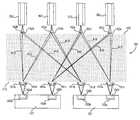
- FIG. 1shows a conceptual view of an embodiment in accordance with the invention.
- Filterless parallel WDM multiplexer element 75is used to direct light from VCSEL configuration 70 , comprising VCSELs 10 , 20 , 30 , 40 to optical fiber 50 .
- the number of VCSELs and lensesmay be increased along with the number of optical fibers.
- Lenses in plane 1such as lenses 11 , 21 , 31 , 41 are typically made just large enough to collect most of the light emitted by VCSELs 10 , 20 , 30 , 40 such as beams 60 , 61 , 62 , 63 , respectively.
- the general design considerationsare as follows. Because a VCSEL typically emits a vertical cone of light, the center of the lens aperture in plane 1 should be aligned with the VCSEL aperture to capture the VCSEL light. In order to direct light from a first lens in a first plane to the appropriate lens in the a second plane, the vertex of the first lens must lie on the line connecting the VCSEL aperture to the center of the appropriate lens aperture in the second plane.
- the first lensis an off-axis section of a lens.
- the appropriate lens in the second planeneeds to be large enough to capture most of the light incident on it and focus this light into the optical fiber.
- the lens in the second planefocuses the incident light into the optical fiber which is positioned to minimize the overall range of angles of the incident light going into the optical fiber.
- the line connecting the optical fiber center with the lens vertexneeds to be parallel to the incident light which by design is parallel to the line connecting the VCSEL aperture to the center of the lens in second plane. This requires that there be an offset between the center of the lens aperture in the second plane and the lens vertex.
- the lens in second planeis also off-axis.
- the other lenses of the multiplexer and any additional optical fibersare similarly positioned.
- the design implementation of WDM multiplexercorrects for these factors and the implementation typically will differ from the above description that, however, results in a baseline design that is qualitatively similar to the actual implementation.
- the qualitative descriptionprovides a starting configuration that may be iteratively modified using ray tracing software packages such as ZEMAX® or CODE V® until the amount of VCSEL light reaching the optical fiber has been optimized.
- VCSEL 10is lined up with the center of lens 11 and lens 11 needs to be large enough to capture most of the light from VCSEL 10 .
- the vertex of lens 11lies in plane 1 on the line defined by VCSEL 10 and the center of lens 12 .
- the vertex of lens 11 and the center of the aperture of lens 10are offset from each other and lens 11 is an off-axis lens.
- Lens 12 in plane 2needs to be sufficiently large to collect most of the light incident on it and focus that light into optical fiber 50 .
- Lens 12focuses most of the incident light into optical fiber 50 which is positioned to minimize the overall range of angles of the incident light that is entering optical fiber 50 .
- lens 12Because lens 12 focuses the light into optical fiber 50 , the line connecting the center of optical fiber 50 needs to be parallel to the incident light. By design, the incident light is parallel to the line connecting the aperture of VCSEL 10 to the center of lens 12 in plane 2 . This requires that the vertex of lens 12 and the center of the aperture of lens 12 are offset from each other. Hence, lens 12 is also an off-axis lens. Similar considerations apply for lenses 21 , 31 , 41 in plane 1 and lenses 22 , 32 , 42 in plane 2 .
- each of VCSELs 10 , 20 , 30 , 40operates at a separate wavelength to generate light beams 60 , 61 , 62 , 63 , each light beam being at a particular wavelength.
- VCSELs 10 , 20 , 30 , 40typically reside on separate die.
- Light beams 60 , 61 , 62 , 63enter filterless parallel WDM multiplexer 75 having two planes of lenses.
- VCSELs 10 , 20 , 30 , 40transmit light beams 60 , 61 , 62 , 63 to lenses 11 , 21 , 31 , 41 residing in first lens plane 1 .
- Lenses 11 , 21 , 31 , 41function to redirect beams 60 , 61 , 62 , 63 into lenses 12 , 22 , 32 , 42 , respectively.
- Lenses 12 , 22 , 32 , 42 residing in second lens plane 2function to direct light beams 60 , 61 , 62 , 63 , respectively, into optical fiber 50 .
- light of four different wavelengthsis multiplexed into optical fiber 50 .
- FIG. 2 ashows an embodiment of a VCSEL array configuration for a parallel WDM transmitter in accordance with the invention.
- Configuration 100 shown in FIG. 2 ais a four wavelength, twelve optical fiber or waveguide configuration constructed from two-dimensional single wavelength monolithic VCSEL arrays.
- the number of die and groups in the configurationmay be increased in accordance with the invention to allow for both more wavelengths and optical fibers or waveguides.
- VCSEL arrays 150 , 160 , 170 , 180each operate at a different wavelength.
- Dies 121 , 122 , 123 , 124are arranged such that each group of square die 101 , 102 , 103 contain VCSEL arrays for each of the four wavelengths. This arrangement ensures that devices of different wavelengths are sufficiently close together to avoid the need for large angle deflections within multiplexer element 75 (i.e. between planes 1 and 2 ) to direct the light beams into optical fiber 50 .
- the need for large angle deflections using refractive lensespresents a cost issue and using diffractive lenses results in higher light losses.
- the substantially square aspect ratio of dies 121 , 122 , 123 , 124improves handleability in the manufacturing environment and reduces handling breakage.
- VCSEL materialis typically brittle and VCSEL structures with a high aspect ratio are inherently more susceptible to damage than VCSEL structures with a low aspect ratio.
- Long VCSEL arrays (high aspect ratio)have proportionally more surface area than square VCSEL arrays (low aspect ratio). For example, a three by three VCSEL array on a 250 ⁇ m pitch has nine devices with a perimeter of 3000 ⁇ m whereas a one by nine VCSEL array also has nine devices but for the same pitch has a 5000 ⁇ m perimeter. Because cracks usually start on the die perimeter, reducing the die perimeter typically increases the VCSEL array yield. Additionally, long VCSEL arrays are typically subject to more stress due to thermally induced stresses resulting from attachment to the substrate material.
- Conventional production toolingis typically designed to handle parts that have a low aspect ratio.
- the majority of semiconductor deviceshave a relatively low aspect ratio (typically an approximately square shape when viewed from the top or bottom) and as a result the conventional production tooling is typically designed to accommodate such low aspect ratio shapes.
- FIG. 2 bshows a simplified view of solder bumps 199 and 599 on the bottom of die 121 and die 515 , respectively (see FIG. 5 ). Solder bumps 199 and 599 act to self align die 121 and die 515 , respectively, during reflow.
- the self-alignment mechanismis due to minimization of the surface tension at each of the individual solder attachment sites so that at each solder attachment site the surface tension is minimized.
- Each solder bumphas a somewhat different volume and wets the bonding pads somewhat differently. The differences are relatively small but cause each solder bump to pull dies 121 and 515 in a different direction. A vector summing of the various forces occurs resulting in the final positioning of die 121 and 515 . Because a two by two VCSEL array has a higher degree of symmetry than a one by twelve VCSEL array, better alignment typically results for a two by two VCSEL array or other VCSEL arrays having a higher degree of symmetry than a one by twelve array VCSEL array.
- the size of two by two VCSEL arrays 150 , 160 , 170 180can be reduced in size to the minimum size needed for solder bumps to attach VCSEL arrays 150 , 160 , 170 , 190 to the substrate. For example, if sufficiently small solder bumps are used to attach two by two VCSEL arrays 150 , 160 , 170 , 180 that are 150 ⁇ m on a side, the VCSEL array size will work with filterless parallel WDM multiplexer 201 (see FIG. 4 ) even if the pitch of the optical fiber array is 250 ⁇ m. In contrast, for one by twelve VCSEL arrays 511 , 521 , 531 , 541 (see FIG.
- the pitch of the VCSEL arrayis constrained by and must match the pitch of the optical fiber array. Because the cost of VCSEL die is proportional to their area cost may be reduced by reducing area. In addition, having a relatively small number of devices per die increases the yield per die. For example, if 5% of the VCSELs in a one by twelve VCSEL arrays 511 , 521 , 531 , 541 are defective, the array yield will be about 54% if the defects are random. For two by two VCSEL arrays 150 , 160 , 170 , 180 with the same defect rate of 5%, the array yield will be 81%. Because yield per die is proportional to cost, smaller arrays are much cheaper.
- FIG. 3 ashows group 101 of FIG. 2 with VCSEL apertures 150 a - 150 d , 160 a - 160 d , 170 a - 170 d , 180 a - 180 d of VCSEL arrays 150 , 160 , 170 , 180 , respectively, labeled to illustrate how light is optically directed from the individual VCSELs into the optical fibers.
- FIG. 3 bshows the portion of first lens plane 210 , corresponding to group 101 , used to multiplex the light from VCSEL arrays 150 , 160 , 170 , 180 into optical fibers for the embodiment in FIG. 1 .
- Each of lenses 151 a-d , 161 a-d , 171 a-d , 181 a-d in first lens plane 210is offset in the horizontal plane with respect to VCSEL apertures 150 a-d , 160 a-d , 170 a-d , 180 a-d , respectively.
- FIG. 3 cshows how light from first lens plane 210 is mapped into lenses 152 a-d , 162 a-d , 172 a-d , 182 a-d in second lens plane 220 as viewed from the optical fiber side.
- Lenses 152 a-d , 162 a-d , 172 a-d , 182 a-d in second lens plane 220are positioned so that light from lens groups 301 , 302 , 303 , 304 is focused into optical fibers 352 , 362 , 372 , 382 , respectively.
- lens group 301has lenses 152 a , 162 c , 182 a , 172 c ;
- lens group 302has lenses 152 c , 162 a , 182 c , 172 c ,
- lens group 303has lenses 152 b , 162 d , 182 b , 172 d ;
- lens group 304has lenses 152 d , 162 b , 182 d , 172 b .
- the axis of each optical fiber 352 , 362 , 372 , 382is aligned with the center of lens groups 304 , 303 , 302 , 301 , respectively.
- Lenses in each lens group 304 , 303 , 302 , 301are positioned such that the four lenses in each group focus the light into optical fibers 352 , 362 , 372 , 382 , respectively.
- Light from lens 151 ais directed to lens 152 a ;
- light from lens 151 bis directed to lens 152 b ;
- light from lens 151 cis directed to lens 152 c ;
- light from lens 151 dis directed to 152 d ;
- light from lens 161 ais directed to lens 162 a ;
- light from lens 161 bis directed to lens 162 b ;
- light from lens 161 cis directed to lens 162 c ;
- light from lens 161 dis directed to lens 162 d ;
- light from lens 171 ais directed to lens 172 a ;
- light from lens 171 bis directed to lens 172 b ;
- FIG. 4shows a side view of the configuration shown in top view in FIGS. 3 a - 3 c showing VCSEL arrays 150 and 160 and the position of optical fibers 352 , 362 , 372 , 382 .
- VCSEL arrays 170 and 180are not shown to aid clarity. Dashed lines in FIG. 4 relate to the hidden VCSEL apertures 160 d , 160 c , 150 d , 150 c and corresponding hidden lenses 161 d , 161 c , 151 d , 151 c.
- FIG. 4shows the mapping by optical multiplexer 201 of light beams 410 , 411 , 412 , 413 , 414 , 415 , 416 , 417 from lens plane 210 to lens plane 220 and into optical fibers 352 , 362 , 372 , 382 .
- Light beam 410originates from VCSEL aperture 160 b passing through lens 161 b to lens 162 b and into optical fiber 352 .
- Light beam 411originates from VCSEL aperture 160 d passing through lens 161 d to lens 162 d and into optical fiber 362 .
- Light beam 414originates from VCSEL aperture 160 a passing through lens 161 a to lens 162 a and into optical fiber 372 .
- Light beam 416originates from VCSEL aperture 160 c passing through lens 161 c to lens 162 c and into optical fiber 382 .
- Light beam 412originates from VCSEL aperture 150 d passing through lens 151 d to lens 152 d and into optical fiber 352 .
- Light beam 413originates from VCSEL aperture 150 b passing through lens 151 b to lens 152 b and into optical fiber 362 .
- Light beam 415originates from VCSEL aperture 150 c passing through lens 151 c to lens 152 c and into optical fiber 372 .
- Light beam 417originates from VCSEL aperture 150 a passing through lens 151 a to lens 152 a and into optical fiber 382 .
- FIG. 5shows an embodiment of VCSEL array configuration 501 in accordance with the invention, each VCSEL array being a one by twelve array.
- Each of die 510 , 520 , 530 , 540contains the same number of VCSELs 515 , 525 , 535 , 545 , respectively, as the number of optical fibers (not shown).
- the embodiment shownis for use with 12 optical fibers and four wavelengths.
- each die 510 , 520 , 530 , 540to be a one by twelve linear array where the width is minimized.
- VCSEL arrays 511 , 521 , 531 , 541might be about 3000 ⁇ m long and only about 200 ⁇ m wide.
- This embodimentminimizes the number of single-wavelength die that need to be used and is amenable to use with a number of multiplexing schemes such as the interference-filter-based zigzag geometry described in U.S. Pat. No. 6,198,864 used in the reverse direction as a multiplexer.
- the high aspect ratio of die 510 , 520 , 530 , 540has the disadvantage that the die are difficult to manipulate, susceptible to breakage and the relatively large number of VCSELs per die reduces the overall yield per die.
- FIG. 6shows an embodiment of VCSEL configuration 601 in accordance with the invention.
- the embodiment shownis for use with 12 optical fibers (not shown) and four wavelengths and uses one die for each VCSEL resulting in 48 die.
- Configuration 601provides the tightest possible spacing of VCSELs of different wavelengths subject to the constraint of one VCSEL per die. Device yield is maximized because there is only one device per die. However, due to the maximization of the number of die, time and cost for assembly are increased.
- VCSEL apertures 615 , 625 , 635 , 645one aperture for each VCSEL, reside on die 620 , 630 , 640 , 650 , respectively.
- the group of four VCSEL apertures 615 , 625 , 635 , 645each typically emitting at a different wavelength, is repeated 12 times to provide a total of 48 VCSEL apertures.
- die 620 , 630 , 640 , 645are arranged into closely spaced two by two groups 661 , 662 , 663 , 664 , 665 , 666 , 667 , 668 , 669 , 670 , 671 , 672 .
- VCSEL apertures 615 , 625 , 635 , 645are positioned so that they are at the inner corners of die 620 , 630 , 640 , 650 .
- configuration 601is merely exemplary and may be modified to accommodate a different number of optical fibers and wavelengths. For example, if more than four wavelengths are to be used, non-rectangular die such as those described in U.S. patent application Ser. No. 10/370,853 filed Feb. 21, 2003 and incorporated by reference may be used in accordance with the invention.
Landscapes
- Physics & Mathematics (AREA)
- General Physics & Mathematics (AREA)
- Optics & Photonics (AREA)
- Optical Couplings Of Light Guides (AREA)
Abstract
Description
Claims (16)
Priority Applications (3)
| Application Number | Priority Date | Filing Date | Title |
|---|---|---|---|
| US10/427,671US7004645B2 (en) | 2003-04-30 | 2003-04-30 | VCSEL array configuration for a parallel WDM transmitter |
| DE60333164TDE60333164D1 (en) | 2003-04-30 | 2003-12-18 | Arrangement of a VCSEL field for a parallel WDM transmitter |
| EP03029344AEP1473579B1 (en) | 2003-04-30 | 2003-12-18 | VCSEL array configuration for a parallel WDM transmitter |
Applications Claiming Priority (1)
| Application Number | Priority Date | Filing Date | Title |
|---|---|---|---|
| US10/427,671US7004645B2 (en) | 2003-04-30 | 2003-04-30 | VCSEL array configuration for a parallel WDM transmitter |
Publications (2)
| Publication Number | Publication Date |
|---|---|
| US20040218875A1 US20040218875A1 (en) | 2004-11-04 |
| US7004645B2true US7004645B2 (en) | 2006-02-28 |
Family
ID=32990452
Family Applications (1)
| Application Number | Title | Priority Date | Filing Date |
|---|---|---|---|
| US10/427,671Expired - LifetimeUS7004645B2 (en) | 2003-04-30 | 2003-04-30 | VCSEL array configuration for a parallel WDM transmitter |
Country Status (3)
| Country | Link |
|---|---|
| US (1) | US7004645B2 (en) |
| EP (1) | EP1473579B1 (en) |
| DE (1) | DE60333164D1 (en) |
Cited By (21)
| Publication number | Priority date | Publication date | Assignee | Title |
|---|---|---|---|---|
| US20050175345A1 (en)* | 2004-01-26 | 2005-08-11 | Mikihiro Shimada | Wavelength multiplexing device and optical transmission module provided with the same |
| US20080068719A1 (en)* | 2004-06-23 | 2008-03-20 | Masatoshi Hayashi | Optical Element, Optical System, and Waveguide |
| US20080077198A1 (en)* | 2006-09-21 | 2008-03-27 | Aculight Corporation | Miniature apparatus and method for optical stimulation of nerves and other animal tissue |
| US7736382B2 (en) | 2005-09-09 | 2010-06-15 | Lockheed Martin Corporation | Apparatus for optical stimulation of nerves and other animal tissue |
| US20100292758A1 (en)* | 2009-01-23 | 2010-11-18 | Lockheed Martin Corporation | Optical stimulation of the brainstem and/or midbrain, including auditory areas |
| US7883536B1 (en) | 2007-01-19 | 2011-02-08 | Lockheed Martin Corporation | Hybrid optical-electrical probes |
| US8012189B1 (en) | 2007-01-11 | 2011-09-06 | Lockheed Martin Corporation | Method and vestibular implant using optical stimulation of nerves |
| US8160696B2 (en) | 2008-10-03 | 2012-04-17 | Lockheed Martin Corporation | Nerve stimulator and method using simultaneous electrical and optical signals |
| US20130051726A1 (en)* | 2011-08-24 | 2013-02-28 | Nistica, Inc. | Asymmetric lenslet array |
| US8475506B1 (en) | 2007-08-13 | 2013-07-02 | Lockheed Martin Corporation | VCSEL array stimulator apparatus and method for light stimulation of bodily tissues |
| US8498699B2 (en) | 2008-10-03 | 2013-07-30 | Lockheed Martin Company | Method and nerve stimulator using simultaneous electrical and optical signals |
| US8652187B2 (en) | 2010-05-28 | 2014-02-18 | Lockheed Martin Corporation | Cuff apparatus and method for optical and/or electrical nerve stimulation of peripheral nerves |
| US8709078B1 (en) | 2011-08-03 | 2014-04-29 | Lockheed Martin Corporation | Ocular implant with substantially constant retinal spacing for transmission of nerve-stimulation light |
| US8747447B2 (en) | 2011-07-22 | 2014-06-10 | Lockheed Martin Corporation | Cochlear implant and method enabling enhanced music perception |
| US8843217B1 (en) | 2013-09-13 | 2014-09-23 | Lockheed Martin Corporation | Combined vestibular and cochlear implant and method |
| US8929973B1 (en) | 2005-10-24 | 2015-01-06 | Lockheed Martin Corporation | Apparatus and method for characterizing optical sources used with human and animal tissues |
| US8945197B1 (en) | 2005-10-24 | 2015-02-03 | Lockheed Martin Corporation | Sight-restoring visual prosthetic and method using infrared nerve-stimulation light |
| US8956396B1 (en) | 2005-10-24 | 2015-02-17 | Lockheed Martin Corporation | Eye-tracking visual prosthetic and method |
| US8996131B1 (en) | 2006-09-28 | 2015-03-31 | Lockheed Martin Corporation | Apparatus and method for managing chronic pain with infrared light sources and heat |
| US9798087B1 (en) | 2016-11-01 | 2017-10-24 | Hewlett Packard Enterprise Development Lp | Optoelectronic devices and wavelength-division multiplexing optical connectors |
| US9846286B2 (en) | 2014-11-27 | 2017-12-19 | Electronics And Telecommunications Research Institute | Wavelength division multi-channel optical module and manufacturing method thereof |
Families Citing this family (9)
| Publication number | Priority date | Publication date | Assignee | Title |
|---|---|---|---|---|
| US7004645B2 (en)* | 2003-04-30 | 2006-02-28 | Agilent Technologies, Inc. | VCSEL array configuration for a parallel WDM transmitter |
| KR101076603B1 (en)* | 2008-07-16 | 2011-10-26 | 옵티시스 주식회사 | Optical communication module for optical wavelength division multipexing |
| US8989530B2 (en) | 2010-07-22 | 2015-03-24 | Avago Technologies General Ip (Singapore) Pte. Ltd. | Optoelectronic modules and submount for same and a method for manufacturing an array of optical devices |
| KR101144665B1 (en)* | 2010-09-20 | 2012-05-24 | 옵티시스 주식회사 | Wavelengh Division Multiplexer and Demultiplexer |
| US9038883B2 (en)* | 2013-09-11 | 2015-05-26 | Princeton Optronics Inc. | VCSEL packaging |
| WO2015065459A1 (en)* | 2013-10-31 | 2015-05-07 | Hewlett-Packard Development Company, L.P. | Multiplexed optoelectronic engines |
| US10924638B2 (en)* | 2016-06-27 | 2021-02-16 | Intel Corporation | Compact, low cost VCSEL projector for high performance stereodepth camera |
| US10527810B2 (en)* | 2017-11-27 | 2020-01-07 | Auxora (Shenzhen) Inc. | Optical interconnect apparatus and system |
| US10564359B2 (en) | 2018-01-04 | 2020-02-18 | Auxora (Shenzhen) Inc. | Optical interconnect apparatus |
Citations (14)
| Publication number | Priority date | Publication date | Assignee | Title |
|---|---|---|---|---|
| US6015998A (en) | 1997-12-17 | 2000-01-18 | Lucent Technolgies, Inc. | Flexibility control in optical materials |
| US6088376A (en) | 1998-03-16 | 2000-07-11 | California Institute Of Technology | Vertical-cavity-surface-emitting semiconductor devices with fiber-coupled optical cavity |
| WO2001075495A2 (en) | 2000-04-04 | 2001-10-11 | Waveguide Solutions, Inc. | Integrated optical circuits |
| US20020009258A1 (en) | 1998-10-26 | 2002-01-24 | Coldren Larry A. | Direct-coupled multimode WDM optical data links with monolithically-integrated multiple-channel VCSEL and photodetector arrays |
| US6353502B1 (en) | 2000-06-13 | 2002-03-05 | Eastman Kodak Company | VCSEL field correction |
| US20020031313A1 (en) | 2000-04-21 | 2002-03-14 | Williams Richard J. | Fiber optic connector |
| US20020041741A1 (en) | 2000-10-06 | 2002-04-11 | Ciemiewicz Jon T. | Optical fiber utilization for VCSEL driven communications |
| US20020067882A1 (en)* | 2000-05-26 | 2002-06-06 | Guilfoyle Peter S. | Virtual optoelectronic crossbar switch |
| US6419404B1 (en)* | 1999-07-01 | 2002-07-16 | The Regents Of The University Of California | Compact multiwavelength transmitter module for multimode fiber optic ribbon cable |
| US20030030910A1 (en)* | 2001-08-08 | 2003-02-13 | Yueh-Ming Teng | Multi-layer antistatic/antireflective coating for video display screen with adjustable light transmission |
| US20040061346A1 (en)* | 2002-09-30 | 2004-04-01 | Intel Corporation | System and method for performing simultaneous precision die bond of photonic components onto a single substrate |
| US6731665B2 (en)* | 2001-06-29 | 2004-05-04 | Xanoptix Inc. | Laser arrays for high power fiber amplifier pumps |
| US20040101247A1 (en)* | 2001-03-13 | 2004-05-27 | Yeou-Yen Chen | Filter based multiplexer/demultiplexer component |
| US20040218875A1 (en)* | 2003-04-30 | 2004-11-04 | Lemoff Brian E. | VCSEL array configuration for a parallel WDM transmitter |
- 2003
- 2003-04-30USUS10/427,671patent/US7004645B2/ennot_activeExpired - Lifetime
- 2003-12-18DEDE60333164Tpatent/DE60333164D1/ennot_activeExpired - Lifetime
- 2003-12-18EPEP03029344Apatent/EP1473579B1/ennot_activeExpired - Lifetime
Patent Citations (14)
| Publication number | Priority date | Publication date | Assignee | Title |
|---|---|---|---|---|
| US6015998A (en) | 1997-12-17 | 2000-01-18 | Lucent Technolgies, Inc. | Flexibility control in optical materials |
| US6088376A (en) | 1998-03-16 | 2000-07-11 | California Institute Of Technology | Vertical-cavity-surface-emitting semiconductor devices with fiber-coupled optical cavity |
| US20020009258A1 (en) | 1998-10-26 | 2002-01-24 | Coldren Larry A. | Direct-coupled multimode WDM optical data links with monolithically-integrated multiple-channel VCSEL and photodetector arrays |
| US6419404B1 (en)* | 1999-07-01 | 2002-07-16 | The Regents Of The University Of California | Compact multiwavelength transmitter module for multimode fiber optic ribbon cable |
| WO2001075495A2 (en) | 2000-04-04 | 2001-10-11 | Waveguide Solutions, Inc. | Integrated optical circuits |
| US20020031313A1 (en) | 2000-04-21 | 2002-03-14 | Williams Richard J. | Fiber optic connector |
| US20020067882A1 (en)* | 2000-05-26 | 2002-06-06 | Guilfoyle Peter S. | Virtual optoelectronic crossbar switch |
| US6353502B1 (en) | 2000-06-13 | 2002-03-05 | Eastman Kodak Company | VCSEL field correction |
| US20020041741A1 (en) | 2000-10-06 | 2002-04-11 | Ciemiewicz Jon T. | Optical fiber utilization for VCSEL driven communications |
| US20040101247A1 (en)* | 2001-03-13 | 2004-05-27 | Yeou-Yen Chen | Filter based multiplexer/demultiplexer component |
| US6731665B2 (en)* | 2001-06-29 | 2004-05-04 | Xanoptix Inc. | Laser arrays for high power fiber amplifier pumps |
| US20030030910A1 (en)* | 2001-08-08 | 2003-02-13 | Yueh-Ming Teng | Multi-layer antistatic/antireflective coating for video display screen with adjustable light transmission |
| US20040061346A1 (en)* | 2002-09-30 | 2004-04-01 | Intel Corporation | System and method for performing simultaneous precision die bond of photonic components onto a single substrate |
| US20040218875A1 (en)* | 2003-04-30 | 2004-11-04 | Lemoff Brian E. | VCSEL array configuration for a parallel WDM transmitter |
Cited By (43)
| Publication number | Priority date | Publication date | Assignee | Title |
|---|---|---|---|---|
| US20050175345A1 (en)* | 2004-01-26 | 2005-08-11 | Mikihiro Shimada | Wavelength multiplexing device and optical transmission module provided with the same |
| US20080068719A1 (en)* | 2004-06-23 | 2008-03-20 | Masatoshi Hayashi | Optical Element, Optical System, and Waveguide |
| US7764428B2 (en)* | 2004-06-23 | 2010-07-27 | Nikon Corporation | Optical element, optical system, and waveguide |
| US8985119B1 (en) | 2005-09-09 | 2015-03-24 | Lockheed Martin Corporation | Method and apparatus for optical stimulation of nerves and other animal tissue |
| US7736382B2 (en) | 2005-09-09 | 2010-06-15 | Lockheed Martin Corporation | Apparatus for optical stimulation of nerves and other animal tissue |
| US8956396B1 (en) | 2005-10-24 | 2015-02-17 | Lockheed Martin Corporation | Eye-tracking visual prosthetic and method |
| US8945197B1 (en) | 2005-10-24 | 2015-02-03 | Lockheed Martin Corporation | Sight-restoring visual prosthetic and method using infrared nerve-stimulation light |
| US8929973B1 (en) | 2005-10-24 | 2015-01-06 | Lockheed Martin Corporation | Apparatus and method for characterizing optical sources used with human and animal tissues |
| US20110238141A1 (en)* | 2006-09-21 | 2011-09-29 | Lockheed Martin Corporation | Miniature method and apparatus for optical stimulation of nerves and other animal tissue |
| US8506613B2 (en) | 2006-09-21 | 2013-08-13 | Lockheed Martin Corporation | Miniature method and apparatus for optical stimulation of nerves and other animal tissue |
| US7988688B2 (en) | 2006-09-21 | 2011-08-02 | Lockheed Martin Corporation | Miniature apparatus and method for optical stimulation of nerves and other animal tissue |
| US20080077200A1 (en)* | 2006-09-21 | 2008-03-27 | Aculight Corporation | Apparatus and method for stimulation of nerves and automated control of surgical instruments |
| US20080077198A1 (en)* | 2006-09-21 | 2008-03-27 | Aculight Corporation | Miniature apparatus and method for optical stimulation of nerves and other animal tissue |
| US8996131B1 (en) | 2006-09-28 | 2015-03-31 | Lockheed Martin Corporation | Apparatus and method for managing chronic pain with infrared light sources and heat |
| US9061135B1 (en) | 2006-09-28 | 2015-06-23 | Lockheed Martin Corporation | Apparatus and method for managing chronic pain with infrared and low-level light sources |
| US8012189B1 (en) | 2007-01-11 | 2011-09-06 | Lockheed Martin Corporation | Method and vestibular implant using optical stimulation of nerves |
| US8551150B1 (en) | 2007-01-11 | 2013-10-08 | Lockheed Martin Corporation | Method and system for optical stimulation of nerves |
| US8317848B1 (en) | 2007-01-11 | 2012-11-27 | Lockheed Martin Corporation | Vestibular implant and method for optical stimulation of nerves |
| US7883536B1 (en) | 2007-01-19 | 2011-02-08 | Lockheed Martin Corporation | Hybrid optical-electrical probes |
| US8357187B1 (en) | 2007-01-19 | 2013-01-22 | Lockheed Martin Corporation | Hybrid optical-electrical probes for stimulation of nerve or other animal tissue |
| US8632577B1 (en) | 2007-01-19 | 2014-01-21 | Lockheed Martin Corporation | Hybrid optical-electrical probes for stimulation of nerve or other animal tissue |
| US8475506B1 (en) | 2007-08-13 | 2013-07-02 | Lockheed Martin Corporation | VCSEL array stimulator apparatus and method for light stimulation of bodily tissues |
| US9011509B2 (en) | 2007-11-30 | 2015-04-21 | Lockheed Martin Corporation | Individually optimized performance of optically stimulating cochlear implants |
| US8998914B2 (en) | 2007-11-30 | 2015-04-07 | Lockheed Martin Corporation | Optimized stimulation rate of an optically stimulating cochlear implant |
| US9011508B2 (en) | 2007-11-30 | 2015-04-21 | Lockheed Martin Corporation | Broad wavelength profile to homogenize the absorption profile in optical stimulation of nerves |
| US8498699B2 (en) | 2008-10-03 | 2013-07-30 | Lockheed Martin Company | Method and nerve stimulator using simultaneous electrical and optical signals |
| US8160696B2 (en) | 2008-10-03 | 2012-04-17 | Lockheed Martin Corporation | Nerve stimulator and method using simultaneous electrical and optical signals |
| US8744570B2 (en) | 2009-01-23 | 2014-06-03 | Lockheed Martin Corporation | Optical stimulation of the brainstem and/or midbrain, including auditory areas |
| US20100292758A1 (en)* | 2009-01-23 | 2010-11-18 | Lockheed Martin Corporation | Optical stimulation of the brainstem and/or midbrain, including auditory areas |
| US8968376B2 (en) | 2010-05-28 | 2015-03-03 | Lockheed Martin Corporation | Nerve-penetrating apparatus and method for optical and/or electrical nerve stimulation of peripheral nerves |
| US8792978B2 (en) | 2010-05-28 | 2014-07-29 | Lockheed Martin Corporation | Laser-based nerve stimulators for, E.G., hearing restoration in cochlear prostheses and method |
| US8864806B2 (en) | 2010-05-28 | 2014-10-21 | Lockheed Martin Corporation | Optical bundle apparatus and method for optical and/or electrical nerve stimulation of peripheral nerves |
| US8652187B2 (en) | 2010-05-28 | 2014-02-18 | Lockheed Martin Corporation | Cuff apparatus and method for optical and/or electrical nerve stimulation of peripheral nerves |
| US8747447B2 (en) | 2011-07-22 | 2014-06-10 | Lockheed Martin Corporation | Cochlear implant and method enabling enhanced music perception |
| US8834545B2 (en) | 2011-07-22 | 2014-09-16 | Lockheed Martin Corporation | Optical-stimulation cochlear implant with electrode(s) at the apical end for electrical stimulation of apical spiral ganglion cells of the cochlea |
| US8840654B2 (en) | 2011-07-22 | 2014-09-23 | Lockheed Martin Corporation | Cochlear implant using optical stimulation with encoded information designed to limit heating effects |
| US8894697B2 (en) | 2011-07-22 | 2014-11-25 | Lockheed Martin Corporation | Optical pulse-width modulation used in an optical-stimulation cochlear implant |
| US8709078B1 (en) | 2011-08-03 | 2014-04-29 | Lockheed Martin Corporation | Ocular implant with substantially constant retinal spacing for transmission of nerve-stimulation light |
| US20130051726A1 (en)* | 2011-08-24 | 2013-02-28 | Nistica, Inc. | Asymmetric lenslet array |
| US9091817B2 (en)* | 2011-08-24 | 2015-07-28 | Nistica, Inc. | Asymmetric lenslet array |
| US8843217B1 (en) | 2013-09-13 | 2014-09-23 | Lockheed Martin Corporation | Combined vestibular and cochlear implant and method |
| US9846286B2 (en) | 2014-11-27 | 2017-12-19 | Electronics And Telecommunications Research Institute | Wavelength division multi-channel optical module and manufacturing method thereof |
| US9798087B1 (en) | 2016-11-01 | 2017-10-24 | Hewlett Packard Enterprise Development Lp | Optoelectronic devices and wavelength-division multiplexing optical connectors |
Also Published As
| Publication number | Publication date |
|---|---|
| US20040218875A1 (en) | 2004-11-04 |
| EP1473579B1 (en) | 2010-06-30 |
| EP1473579A1 (en) | 2004-11-03 |
| DE60333164D1 (en) | 2010-08-12 |
Similar Documents
| Publication | Publication Date | Title |
|---|---|---|
| US7004645B2 (en) | VCSEL array configuration for a parallel WDM transmitter | |
| KR101520143B1 (en) | Optical engine for point-to-point communications | |
| US7817883B2 (en) | Optical assembly and method of making same | |
| US7184621B1 (en) | Multi-wavelength transmitter optical sub assembly with integrated multiplexer | |
| EP3687008B1 (en) | Light source unit | |
| US7444046B2 (en) | Diode laser array coupling optic and system | |
| US20070291373A1 (en) | Coupling devices and methods for laser emitters | |
| US7076129B2 (en) | Apparatus and method for a filterless parallel WDM multiplexer | |
| US6591042B2 (en) | Fiber based wavelength de-multiplexing system | |
| US9671576B1 (en) | CWDM transceiver module | |
| US7466502B2 (en) | Optical wavelength division coupler and associated methods | |
| US6870195B2 (en) | Array of discretely formed optical signal emitters for multi-channel communication | |
| US6768838B2 (en) | Optical module | |
| US20040114655A1 (en) | Transmitter array with pixel element that has primary semiconductor laser and at least one secondary semiconductor laser | |
| US6989945B2 (en) | Long-throw, tight focusing optical coupler | |
| US7061517B2 (en) | Exposure head | |
| JP2005241730A (en) | Optical multiplexer/demultiplexer and optical module | |
| JP5900043B2 (en) | Optical coupling structure and array optical amplification module | |
| KR102066971B1 (en) | Fiber array structure for fiber lase with improving chnnel and fiber array method for fiber lase | |
| KR101211790B1 (en) | Multi-channel transmitter for optic interface | |
| KR101090666B1 (en) | Multichannel Transmitters for Optical Interfaces | |
| EP3422615B1 (en) | Filter block for an n-channel multiplexing/demultiplexing device and optical wavelength division/demultiplexing device | |
| US20060215950A1 (en) | Integrated optical systems for generating an array of beam outputs | |
| GB2492349A (en) | Photonic assembly | |
| JPH02101406A (en) | Parallel transmission optical module |
Legal Events
| Date | Code | Title | Description |
|---|---|---|---|
| AS | Assignment | Owner name:AGILENT TECHNOLOGIES, INC., COLORADO Free format text:ASSIGNMENT OF ASSIGNORS INTEREST;ASSIGNORS:LEMOFF, BRIAN E.;WILSON, ROBERT E.;REEL/FRAME:013991/0782 Effective date:20030430 | |
| STCF | Information on status: patent grant | Free format text:PATENTED CASE | |
| AS | Assignment | Owner name:AVAGO TECHNOLOGIES GENERAL IP PTE. LTD.,SINGAPORE Free format text:ASSIGNMENT OF ASSIGNORS INTEREST;ASSIGNOR:AGILENT TECHNOLOGIES, INC.;REEL/FRAME:017206/0666 Effective date:20051201 Owner name:AVAGO TECHNOLOGIES GENERAL IP PTE. LTD., SINGAPORE Free format text:ASSIGNMENT OF ASSIGNORS INTEREST;ASSIGNOR:AGILENT TECHNOLOGIES, INC.;REEL/FRAME:017206/0666 Effective date:20051201 | |
| AS | Assignment | Owner name:AVAGO TECHNOLOGIES FIBER IP (SINGAPORE) PTE. LTD., Free format text:ASSIGNMENT OF ASSIGNORS INTEREST;ASSIGNOR:AVAGO TECHNOLOGIES GENERAL IP (SINGAPORE) PTE. LTD.;REEL/FRAME:017675/0199 Effective date:20060127 | |
| FPAY | Fee payment | Year of fee payment:4 | |
| FPAY | Fee payment | Year of fee payment:8 | |
| AS | Assignment | Owner name:AVAGO TECHNOLOGIES GENERAL IP (SINGAPORE) PTE. LTD Free format text:MERGER;ASSIGNOR:AVAGO TECHNOLOGIES FIBER IP (SINGAPORE) PTE. LTD.;REEL/FRAME:030369/0672 Effective date:20121030 | |
| AS | Assignment | Owner name:DEUTSCHE BANK AG NEW YORK BRANCH, AS COLLATERAL AGENT, NEW YORK Free format text:PATENT SECURITY AGREEMENT;ASSIGNOR:AVAGO TECHNOLOGIES GENERAL IP (SINGAPORE) PTE. LTD.;REEL/FRAME:032851/0001 Effective date:20140506 Owner name:DEUTSCHE BANK AG NEW YORK BRANCH, AS COLLATERAL AG Free format text:PATENT SECURITY AGREEMENT;ASSIGNOR:AVAGO TECHNOLOGIES GENERAL IP (SINGAPORE) PTE. LTD.;REEL/FRAME:032851/0001 Effective date:20140506 | |
| AS | Assignment | Owner name:AVAGO TECHNOLOGIES GENERAL IP (SINGAPORE) PTE. LTD., SINGAPORE Free format text:TERMINATION AND RELEASE OF SECURITY INTEREST IN PATENT RIGHTS (RELEASES RF 032851-0001);ASSIGNOR:DEUTSCHE BANK AG NEW YORK BRANCH, AS COLLATERAL AGENT;REEL/FRAME:037689/0001 Effective date:20160201 Owner name:AVAGO TECHNOLOGIES GENERAL IP (SINGAPORE) PTE. LTD Free format text:TERMINATION AND RELEASE OF SECURITY INTEREST IN PATENT RIGHTS (RELEASES RF 032851-0001);ASSIGNOR:DEUTSCHE BANK AG NEW YORK BRANCH, AS COLLATERAL AGENT;REEL/FRAME:037689/0001 Effective date:20160201 | |
| AS | Assignment | Owner name:BANK OF AMERICA, N.A., AS COLLATERAL AGENT, NORTH CAROLINA Free format text:PATENT SECURITY AGREEMENT;ASSIGNOR:AVAGO TECHNOLOGIES GENERAL IP (SINGAPORE) PTE. LTD.;REEL/FRAME:037808/0001 Effective date:20160201 Owner name:BANK OF AMERICA, N.A., AS COLLATERAL AGENT, NORTH Free format text:PATENT SECURITY AGREEMENT;ASSIGNOR:AVAGO TECHNOLOGIES GENERAL IP (SINGAPORE) PTE. LTD.;REEL/FRAME:037808/0001 Effective date:20160201 | |
| AS | Assignment | Owner name:AVAGO TECHNOLOGIES GENERAL IP (SINGAPORE) PTE. LTD Free format text:CORRECTIVE ASSIGNMENT TO CORRECT THE ASSIGNEE NAME PREVIOUSLY RECORDED AT REEL: 017206 FRAME: 0666. ASSIGNOR(S) HEREBY CONFIRMS THE ASSIGNMENT;ASSIGNOR:AGILENT TECHNOLOGIES, INC.;REEL/FRAME:038632/0662 Effective date:20051201 | |
| AS | Assignment | Owner name:AVAGO TECHNOLOGIES GENERAL IP (SINGAPORE) PTE. LTD., SINGAPORE Free format text:TERMINATION AND RELEASE OF SECURITY INTEREST IN PATENTS;ASSIGNOR:BANK OF AMERICA, N.A., AS COLLATERAL AGENT;REEL/FRAME:041710/0001 Effective date:20170119 Owner name:AVAGO TECHNOLOGIES GENERAL IP (SINGAPORE) PTE. LTD Free format text:TERMINATION AND RELEASE OF SECURITY INTEREST IN PATENTS;ASSIGNOR:BANK OF AMERICA, N.A., AS COLLATERAL AGENT;REEL/FRAME:041710/0001 Effective date:20170119 | |
| FPAY | Fee payment | Year of fee payment:12 | |
| AS | Assignment | Owner name:AVAGO TECHNOLOGIES INTERNATIONAL SALES PTE. LIMITE Free format text:MERGER;ASSIGNOR:AVAGO TECHNOLOGIES GENERAL IP (SINGAPORE) PTE. LTD.;REEL/FRAME:047196/0097 Effective date:20180509 | |
| AS | Assignment | Owner name:AVAGO TECHNOLOGIES INTERNATIONAL SALES PTE. LIMITE Free format text:CORRECTIVE ASSIGNMENT TO CORRECT THE EXECUTION DATE PREVIOUSLY RECORDED AT REEL: 047196 FRAME: 0097. ASSIGNOR(S) HEREBY CONFIRMS THE MERGER;ASSIGNOR:AVAGO TECHNOLOGIES GENERAL IP (SINGAPORE) PTE. LTD.;REEL/FRAME:048555/0510 Effective date:20180905 | |
| AS | Assignment | Owner name:BROADCOM INTERNATIONAL PTE. LTD., SINGAPORE Free format text:ASSIGNMENT OF ASSIGNORS INTEREST;ASSIGNOR:AVAGO TECHNOLOGIES INTERNATIONAL SALES PTE. LIMITED;REEL/FRAME:053771/0901 Effective date:20200826 | |
| AS | Assignment | Owner name:AVAGO TECHNOLOGIES INTERNATIONAL SALES PTE. LIMITED, SINGAPORE Free format text:MERGER;ASSIGNORS:AVAGO TECHNOLOGIES INTERNATIONAL SALES PTE. LIMITED;BROADCOM INTERNATIONAL PTE. LTD.;REEL/FRAME:062952/0850 Effective date:20230202 |