US7002825B2 - Word line arrangement having segmented word lines - Google Patents
Word line arrangement having segmented word linesDownload PDFInfo
- Publication number
- US7002825B2 US7002825B2US11/103,184US10318405AUS7002825B2US 7002825 B2US7002825 B2US 7002825B2US 10318405 AUS10318405 AUS 10318405AUS 7002825 B2US7002825 B2US 7002825B2
- Authority
- US
- United States
- Prior art keywords
- word line
- array
- integrated circuit
- word
- lines
- Prior art date
- Legal status (The legal status is an assumption and is not a legal conclusion. Google has not performed a legal analysis and makes no representation as to the accuracy of the status listed.)
- Expired - Lifetime
Links
- 230000008878couplingEffects0.000claimsdescription2
- 238000010168coupling processMethods0.000claimsdescription2
- 238000005859coupling reactionMethods0.000claimsdescription2
- 238000003491arrayMethods0.000description32
- 238000010586diagramMethods0.000description17
- 238000000034methodMethods0.000description14
- 238000005516engineering processMethods0.000description10
- 239000004065semiconductorSubstances0.000description8
- 238000004519manufacturing processMethods0.000description7
- 238000013461designMethods0.000description6
- 230000002829reductive effectEffects0.000description6
- 230000008901benefitEffects0.000description5
- 230000000694effectsEffects0.000description5
- 238000011161developmentMethods0.000description4
- 230000018109developmental processEffects0.000description4
- 230000008520organizationEffects0.000description4
- 238000012360testing methodMethods0.000description4
- 230000008569processEffects0.000description3
- 230000002441reversible effectEffects0.000description3
- 239000000758substrateSubstances0.000description3
- 230000003213activating effectEffects0.000description2
- 239000000463materialSubstances0.000description2
- 239000002184metalSubstances0.000description2
- 239000011368organic materialSubstances0.000description2
- 230000003071parasitic effectEffects0.000description2
- 239000000047productSubstances0.000description2
- 230000009467reductionEffects0.000description2
- 10171019098150S ribosomal protein L6Proteins0.000description1
- XUIMIQQOPSSXEZ-UHFFFAOYSA-NSiliconChemical compound[Si]XUIMIQQOPSSXEZ-UHFFFAOYSA-N0.000description1
- 230000003542behavioural effectEffects0.000description1
- 230000015572biosynthetic processEffects0.000description1
- 239000003990capacitorSubstances0.000description1
- 230000015556catabolic processEffects0.000description1
- 230000008859changeEffects0.000description1
- 238000004891communicationMethods0.000description1
- 230000002860competitive effectEffects0.000description1
- 230000003247decreasing effectEffects0.000description1
- 230000002939deleterious effectEffects0.000description1
- 230000001419dependent effectEffects0.000description1
- 230000001627detrimental effectEffects0.000description1
- 238000007599dischargingMethods0.000description1
- 230000009977dual effectEffects0.000description1
- 230000005684electric fieldEffects0.000description1
- 230000014509gene expressionEffects0.000description1
- 239000002784hot electronSubstances0.000description1
- 230000001788irregularEffects0.000description1
- 230000000670limiting effectEffects0.000description1
- 230000007774longtermEffects0.000description1
- 238000012986modificationMethods0.000description1
- 230000004048modificationEffects0.000description1
- 230000003287optical effectEffects0.000description1
- 239000012782phase change materialSubstances0.000description1
- 238000012545processingMethods0.000description1
- 229910052710siliconInorganic materials0.000description1
- 239000010703siliconSubstances0.000description1
- 238000004088simulationMethods0.000description1
- 239000007787solidSubstances0.000description1
- 230000003068static effectEffects0.000description1
- 239000013589supplementSubstances0.000description1
- 230000000007visual effectEffects0.000description1
Images


Classifications
- G—PHYSICS
- G11—INFORMATION STORAGE
- G11C—STATIC STORES
- G11C8/00—Arrangements for selecting an address in a digital store
- G11C8/08—Word line control circuits, e.g. drivers, boosters, pull-up circuits, pull-down circuits, precharging circuits, for word lines
- H—ELECTRICITY
- H10—SEMICONDUCTOR DEVICES; ELECTRIC SOLID-STATE DEVICES NOT OTHERWISE PROVIDED FOR
- H10B—ELECTRONIC MEMORY DEVICES
- H10B69/00—Erasable-and-programmable ROM [EPROM] devices not provided for in groups H10B41/00 - H10B63/00, e.g. ultraviolet erasable-and-programmable ROM [UVEPROM] devices
Definitions
- the present inventionrelates to semiconductor integrated circuits containing memory arrays, and in preferred embodiments the invention particularly relates to monolithic three-dimensional memory arrays.
- a three-dimensional (3D) memory arrayis most efficient when the number of cell on each bit line and word line is large. This number of cells is frequently called the fan-out (N) of the bit line and the word line.
- NThis number of cells is frequently called the fan-out (N) of the bit line and the word line.
- a large fan-outreduces the number of vertical connections between the array lines on each memory layer and the circuitry below. These vertical connections cannot lie beneath the individual memory cells on each layer, and thus may add significantly to the chip area. But a large fan-out frequently has certain electrical disadvantages depending on the memory cell technology being used. For example, the capacitance of array lines and the resistance of array lines may increase by the fan-out (N) factor, and leakage per cell may cause power dissipation to increase by a factor of N 2 .
- N 2Another deleterious effect proportional to N 2 is the reverse bias stress on unselected cells in a passive element memory array.
- unselected antifuse (AF) memory cellsfrequently have a large reverse bias during write conditions which can degrade the reliability of un-programmed cells if the voltage stress is maintained for a long period of time.
- the stress time on each cellis dependent upon the length of time that is necessary to write all the cells within a common group.
- the common group of cellsmay be as large in number as the fan-out of the word line (N) times the fan-out of the bit line, or N 2 .
- Nword line
- Flash EEPROM deviceswhich segment the bit lines
- DRAMsdynamic RAMs
- SRAMsstatic RAMs
- Such deviceshave the segment switches on one layer (e.g., within the silicon substrate), and have a different layer of memory cells with segmented lines, and one layer of long lines (e.g., global lines).
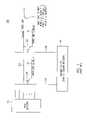
- FIG. 1such a traditional segmented word line arrangement 100 is shown.
- a row decoder 102generates a plurality of global word lines, such as global word line 103 , which traverse across all or a portion of a memory array or sub-array.
- a segment select block 104(which may be part of a column decoder circuit) generates a pair of segment select lines 105 , 108 for coupling a selected one of segments 107 , 110 through a respective device 106 , 109 to the global word line 103 .
- the global word lineswhich run parallel to the word line segments, serve as bias lines to which a select word line segment is coupled.
- the present inventionprovides, in certain embodiments, a three-dimensional high-density passive element memory cell array with short word lines while still maintaining a small support circuit area for efficiency.
- the word linesare preferably formed of short, low resistance word line segments on two or more word line layers which are connected together in parallel to form a given word line. No segment switch devices are employed between the word line segments.
- a shared vertical connectionpreferably connects the word line segments together and further connects the word line to a word line driver circuit disposed generally below the word line.
- the word line driver circuitcouples an associated word line to either a selected bias line or an unselected bias line associated with the driver circuit.
- An array with a lower fan-out in one directionreduces the total stress time on unselected cells. If the fan-out for the word line is n, and which is a much smaller number than the fan out of the bit line (N), the stress time on unselected cells is proportional to n times N. Thus, the stress time is greatly reduced by decreasing the fan-out of just the word line.
- AF memory arraysprogram only one bit at a time in the group so that the energy needed to program the AF is dedicated to one selected memory cell (e.g., one bit). As that one cell breaks down, high currents flow in the long bit lines and word lines. A second cell on either the bit line or the word line would typically be robbed of the needed energy to program successfully. However, if the word line is very short and driven by low resistance drivers, the energy of a first programmed cell on the word line would have little effect on other programmed cells on the word line.
- each simultaneously programmed cell on the word lineresides on a different bit line (to preserve the respective logic value for each bit), the current along any bit line is no higher than for programming a single memory cell. Consequently, interference due to currents in the array lines is avoided by reducing the word line fan-out, without requiring a reduction in the bit line fan-out.
- Thisallows the simultaneous programming of multiple bits on one word line, and directly reduces the stress time endured by the unselected cells in the group.
- the stress time of unselected bitsis greatly reduced.
- the programming of multiple bits at a time on one word linehas the additional benefit of increasing write bandwidth.
- a three-dimensional memory arrayit is preferable to select cells for programming on multiple layers, and more preferably on each of the layers, to reduce stress time. This is particularly valuable for mirrored 3D structures in which selecting a cell on a single memory layer produces stress to unselected cells on multiple layers.
- memory cellsmay be selected on two memory layers without producing stress on additional memory layers. Although selecting a cell on a layer stresses that layer, no additional layers are stressed (e.g., only one layer stressed per selected memory cell).
- the passive element memory arraymay incorporate write-once memory cells or memory cells that have a less extreme change in conductivity, and may be fuse-type cells or anti-fuse type cells.
- the memory cellspreferably include antifuse memory cells, and the memory array preferably is a half-mirrored memory array having respective word line layers shared by two respective bit line layers that are not shared with other word line layers. In other words, each memory plane preferably includes a unique bit line layer but a shared word line layer.
- the present inventionprovides a three-dimensional electrically programmable read-only memory (EPROM) array having word lines formed by multiple layers of word line segments which are connected by a shared vertical connection to an associated word line driver circuit.
- EPROMelectrically programmable read-only memory
- such memory arraysmay be realized with array blocks having a very large number of word lines and a relatively small number of bit lines.
- an exemplary array blockmay include around 8000 word lines on a word line layer, but only about 100 bit lines on a bit line layer. As a result, the length of each word line segment forming the word lines is kept very short, while the length of the bit lines is considerably larger.
- the inventionin several aspects is suitable for integrated circuits having a memory array, for memory cell and memory array structures, for methods for operating such integrated circuits and memory arrays, for methods for forming or fabricating such integrated circuits and memory arrays, and for computer readable media encodings of such integrated circuits or memory arrays, all as described herein in greater detail and as set forth in the appended claims.
- FIG. 1is a schematic diagram of a traditional segmented word line arrangement.
- FIG. 2is a schematic diagram representing a three-dimensional memory array having a segmented word line arrangement in accordance with certain embodiments of the present invention.
- FIG. 3is a cross-section view of a three-dimensional memory array having a segmented word line arrangement in accordance with certain embodiments of the present invention, which shows a half-mirrored memory array having word line layers shared by two bit line layers.
- FIG. 4is a cross-section view representing a three-dimensional memory array having a segmented word line arrangement in accordance with certain embodiments of the present invention, which shows two groups of word line layers, and which in this exemplary configuration shows a fully-mirrored memory array having bit line layers shared by two word line layers.
- FIG. 5is a top view representing a word line layer and a bit line layer of a three-dimensional memory array in accordance with certain embodiments of the present invention, which shows 2:1 interleaved word line segments, where vertical connections to half of the word line segments for a block are on the left side of the block, and vertical connections to the other half of the word line segments for the block are on the right side of the block.
- a word line segment from two adjacent blocksshares each vertical connection.
- FIG. 6is a top view representing a word line layer and associated vertical connections, in accordance with certain embodiments of the present invention, which shows non-interleaved word line segments, where vertical connections to the word line segments for a block are on one side of the block. The vertical connections are not shared by more than one block.
- FIG. 7is a top view representing a word line layer and associated vertical connections, in accordance with certain embodiments of the present invention, which shows 2:1 interleaved word line segments, where vertical connections to half of the word line segments for a block are on the left side of the block, and vertical connections to the other half of the word line segments for the block are on the right side of the block.
- the vertical connectionsare not shared by more than one block.
- FIG. 8is a top view representing a word line layer and associated vertical connections, in accordance with certain embodiments of the present invention, which shows non-interleaved word line segments, where vertical connections to the word line segments for a block are on one side of the block, and where a word line segment from two adjacent blocks shares each vertical connection.
- FIG. 9is a schematic diagram representing a multi-headed word line decoder having bias lines traversing perpendicular to the word line segments and having a row select line traversing parallel to the word line segments.
- FIG. 10is a schematic diagram representing a multi-headed word line decoder having multiple four-headed driver circuits, such as that depicted in FIG. 9 , spaced across at least a portion of the memory array.
- FIG. 11is a block diagram of an exemplary memory array and associated support circuitry, in accordance with certain embodiments of the present invention, having a single multi-headed row decoder supporting 76 memory array blocks of 130 cells each, and having interleaved bit lines, half of which are supported by column decoder and sense/programming circuitry at the top of the array, and the other half of which are supported by column decoder and sense/programming circuitry at the bottom of the array.
- FIG. 12is a top view representing a word line layer and a bit line layer of a three-dimensional memory array, which shows four blocks having 2:1 interleaved word line segments and shared vertical connections, as in FIG. 6 , and which illustrates activating a single array block for certain embodiments and activating a pair of adjacent array blocks for certain other embodiments.
- FIG. 13is a schematic diagram representing a bias control circuit for a multi-headed word line decoder, having a first circuit for discharging the bias line from an initial high voltage to a lower voltage, and having a second circuit which is distributed along the length of the bias line for providing a low impedance connection to a ground plane.
- FIG. 14is a block diagram of an exemplary memory array and certain associated support circuitry, in accordance with some embodiments of the present invention, having a row decoder on each of the left and right sides of the memory array, and having three column decoder and bit line circuits, respectively at the top, middle, and bottom of the array to support an upper and lower sub-array of 2:1 interleaved bit lines.
- An exemplary word line driver circuit bias lineis shown with a distributed grounding circuit depicted, such as that shown in FIG. 13 .
- Also depictedis a representation of a power grid for providing a robust local ground throughout the array to the respective distributed discharge circuits on the various word line driver circuit bias lines.
- FIG. 15is a cross-section diagram representing a half-mirrored memory array having two vertically-connected word line layers, each shared by two bit line layers, in accordance with certain embodiments of the present invention.
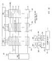
- FIG. 2a schematic diagram is shown representing a three-dimensional memory array having a segmented word line arrangement in accordance with certain embodiments of the present invention.
- Each word lineis formed by one or more word line segments on at least one, and advantageously more than one, word line layer of the memory array.
- a first word lineis formed by word line segment 130 disposed on one word line layer of the memory array and by word line segment 132 disposed on another word line layer.
- the word line segments 130 , 132are connected by a vertical connection 128 to form the first word line.
- the vertical connection 128also provides a connection path to a driver device 126 disposed in another layer (e.g., within the semiconductor substrate).
- a decoded output 122 from a row decodertraverses substantially parallel to the word line segments 130 , 132 and when selected, couples the word line segments 130 , 132 through device 126 to a decoded bias line 124 which traverses substantially perpendicular to the word line segments.
- word line segments 131 , 133which are connected by a vertical connection 129 to form a second word line and to provide a connection path to driver device 127 .
- Another decoded output 123 from the row decodercouples, when selected, these word line segments 131 , 133 through device 127 to the decoded bias line 124 . While this figure conceptually introduces the invention, many embodiments are described herebelow which include variations to the configuration shown, and moreover include details which may be appropriate for certain embodiments but not necessarily for all embodiments.
- FIG. 3is a cross-section view of a three-dimensional half-mirrored memory array having word line layers each respectively shared by two bit line layers.
- Three word line layersare depicted, labeled WL 2 , WL 5 , and WL 8 .
- the word line segments on layer WL 8are shared by bit lines on bit line layers BL 7 and BL 9 .
- the word line layer WL 5is shared by bit line layers BL 4 and BL 6
- the word line layer WL 2is shared by bit line layers BL 1 and BL 3 .
- Word line segments 132 , 130 , and 142are connected by vertical connection 128 to form a word line.
- a plurality of bit lines 144is shown on bit line layer BL 9 .
- a plurality of memory cells 146is formed between each bit line 144 and the word line segment 142 .
- a plurality of memory cells 148is formed between each bit line 150 (on layer BL 7 ) and the word line segment 142 .
- Other word line layersare similarly arranged, as shown.
- FIG. 4is a cross-section view representing a three-dimensional fully-mirrored memory array having a segmented word line arrangement in accordance with certain embodiments of the present invention, which shows two groups of word line layers.
- One or more word line segments on each of layers WL 1 , WL 5 , and WL 9are connected (e.g., by vertical connection 174 ) to form a word line, while one or more word line segments on each of layers WL 3 , WL 7 , and WL 11 are connected (e.g., by vertical connection 172 ) to form a word line.
- a plurality of bit lines 166is shown on bit line layer BL 10 .
- a plurality of memory cells 168is respectively formed between each bit line 166 and the word line segment 162 (on layer WL 11 ).
- a plurality of memory cells 170is respectively formed between each bit line 166 and the word line segment 164 (on layer WL 9 ).
- Other word line layersare similarly arranged, as shown, providing a total of ten memory planes for this exemplary structure. If an additional bit line layer were provided below the WL 1 layer, and an additional bit line layer were provided above the WL 11 layer, then a total of twelve memory planes would be provided.
- Selectivity of the memory arrayis accomplished by selecting one word line associated with a bit line layer but not the other.
- driver circuitrymay drive vertical connection 172 and its connected word line segments to an active level while keeping vertical connection 174 and its connected word line segments at an inactive level, to select one or more memory cells 168 (depending upon how many bit lines are selected) while keeping memory cells 170 unselected (or at least “half-selected” for those sharing a selected bit line 166 ).
- Each vertical connection in the figureis shared by two word line segments on an associated word line layer. For example, word line segments 176 and 178 share the vertical connection 174 .
- Other configurations of word line segments and associated vertical connectionsare described in greater detail below.
- the word line arrangement shown in FIG. 4may also be utilized with half-mirrored memory arrays having word line layers shared by two bit line layers, similarly to that shown in FIG. 3 .
- the memory arraywould include up to twelve memory planes since each word line layer would be associated with two memory planes.
- FIG. 5is a top view representing a word line layer and a bit line layer of a three-dimensional memory array in accordance with certain embodiments of the present invention.
- Memory blocks 182 , 184are shown respectively including a plurality of bit lines 183 , 185 , and having 2:1 interleaved word line segments.
- Vertical connections to half of the word line segments for a blockare on the left side of the block (e.g., word line segment 187 and vertical connection 189 ), and vertical connections to the other half of the word line segments for the block are on the right side of the block (e.g., word line segment 186 and vertical connection 190 ).
- each vertical connectionserves a word line segment in each of two adjacent blocks.
- vertical connection 190connects to word line segment 186 in array block 182 and connects to word line segment 188 in array block 184 .
- each vertical connection(such as vertical connection 190 ) is shared by a word line segment in each of two adjacent blocks.
- the respective “outside” vertical connections for the first and last array blocksmay serve only word line segments in the first and last array blocks.
- block 184is the last block of a plurality of blocks forming a memory array
- its outside vertical connectionse.g., vertical connection 194
- the pitch of the vertical connectionsis twice the pitch of the individual word line segments themselves. This is particularly advantageous since the word line pitch which is achievable for many passive element memory cell arrays is significantly smaller than achievable for many via structures which might be employed to form the vertical connections. Moreover, as described in greater detail below, this also may reduce the complexity of the word line driver circuitry to be implemented in the semiconductor substrate below the memory array.
- FIG. 6is a top view representing a word line layer and associated vertical connections, which shows non-interleaved word line segments, where vertical connections to the word line segments for a block are on one side of the block.
- the vertical connectionscould all be on the same side of its associated block (as shown here on the left side of each block), or could be alternated such that a double column of vertical connections occurs between every other array block.
- the vertical connectionsare not shared by more than one block.
- FIG. 7is a top view representing a word line layer and associated vertical connections, which shows 2:1 interleaved word line segments, where vertical connections to half of the word line segments for a block are on the left side of the block, and vertical connections to the other half of the word line segments for the block are on the right side of the block.
- the vertical connectionsare not shared by more than one block.
- the vertical connections between each blockmay be arranged in a single column, which reduces the lateral spacing between adjacent blocks but which requires a vertical connection pitch equal to the word line pitch, or may be staggered as shown to relax the required spacing between vertical connections at a small expense in block-to-block spacing.
- FIG. 8is a top view representing a word line layer and associated vertical connections, which shows non-interleaved word line segments, where vertical connections to the word line segments for a block are on one side (but not both sides) of the block, and where a word line segment from two adjacent blocks shares each vertical connection.
- FIG. 9is a schematic diagram representing a multi-headed word line decoder configuration 230 having bias lines traversing perpendicular to the word line segments and having decoded row select lines (sometimes referred to herein as a “select node”) traversing parallel to the word line segments.
- a row decoder 232generates a plurality of decoded row select lines, one of which is labeled 234 .
- An array block select circuit 235generates an unselected bias level BiasU on node 236 , and generates four decoded bias levels BiasA, BiasB, BiasC, and BiasD respectively on nodes 238 , 240 , 242 , and 244 .
- a quad word line driver circuit 233includes four separate word line driver circuits 254 , each for driving a respective word line to the unselected bias line BiasU (when the row select 234 is unselected) or to a respective one of the four “selected” bias lines BiasA, BiasB, BiasC, and BiasD (when the row select 234 is selected).
- a first transistor 256drives the word line 248 (by way of the vertical connection 260 ) to the unselected bias level BiasU when the row select 234 is low, as would be the case for all the unselected row select lines generated by the row decoder 232 .
- a second transistor 258drives the word line 248 (also labeled ROW B, which typically includes one or more word line segments on each of more than one word line layer) to the associated bias level BiasB when the row select 234 is high, as would be the case for the one “selected” row select line generated by the row decoder 232 .
- each of the word lines 246 , 248 , 250 , and 252is respectively driven to its associated bias line BiasA, BiasB, BiasC, and BiasD.
- One of the bias lines BiasA, BiasB, BiasC, and BiasDis driven to a selected level, while the remaining three of the bias lines are maintained at an unselect bias level, such as the BiasU level. Consequently, one of the four word lines 246 , 248 , 250 , and 252 is respectively driven to the selected bias level while the remaining three word lines remain at the unselected bias level.
- the row select 234is selected when it is high, and unselected when it is low, and the unselected bias level BiasU is higher than the selected one of the four bias levels BiasA, BiasB, BiasC, and BiasD. Consequently the transistor 256 is advantageously implemented as P-channel device and the transistor 258 as an N-channel device.
- Exemplary voltages for memory array incorporating antifuse memory cellsare a selected bias level of 0 volts and an unselected bias level BiasU of nominally 8 volts. In other embodiments the polarity of the voltages, and the polarity of the driver transistors 256 , 258 may be reversed.
- driver devicesmay be utilized, such as two N-channel transistors, depending on the particular memory cell technology and the desired unselected and selected word line voltages. While four such decoded selected bias lines are described above, in other embodiments two such lines may be provided, with each row select node consequently being coupled to two word line driver circuits within each group of drivers, or even just one selected bias line provided in other embodiments.
- FIG. 10is a schematic diagram representing a multi-headed word line decoder having multiple four-headed driver circuits, such as that depicted in FIG. 9 , spaced across at least a portion of the memory array.
- the row decoder 232generates a plurality of decoded row select lines, one of which is labeled 234 , as before.
- An array block select circuit 235generates an unselected bias level BiasU, and generates four decoded bias levels BiasA, BiasB, BiasC, and BiasD, here labeled as U, A, B, C, and D.
- Each of a vertical group 282 of quad word line driver circuits 233is responsive to a respective one of the row select lines generated by the row decoder 232 . All of the quad word line driver circuits 233 within the group 282 are associated with the U, A, B, C, and D bias lines, as suggested by the configuration shown in FIG. 9 .
- the array block select circuit 235also generates another respective set of bias lines for each of two additional groups 284 , 286 of quad word line driver circuits 233 .
- the second set of bias linesincludes an unselected bias level BiasU, and generates four decoded bias levels BiasE, BiasF, BiasG, and BiasH, here labeled as U, E, F, G, and H.
- the third set of bias linesincludes an unselected bias level BiasU, and generates four decoded bias levels Biasl, BiasJ, BiasK, and BiasL, here labeled as U, I, J, K, and L.
- one quad word line driver circuit 233 in each of the groups 282 , 284 , and 286is responsive to the row select 234 signal, and the array block select circuit 235 may be implemented to decode the bias lines A, B, C, . . . , K, L so that only one such bias line is selected (i.e., driven to the selected bias level). As a result, only one word line associated with row select 234 is selected, and the remaining eleven word lines that are associated with row select 234 remain unselected.
- Each word line driver 254may be assumed for this embodiment to be coupled to a word line segment in each of two adjacent array blocks (e.g., an array such as that shown in FIG. 5 ). Consequently, two bit line select circuits 288 , 290 are associated with the group 282 of word line driver circuits, one for each of the two adjacent array blocks having word lines driven by the group 282 .
- Each bit line select circuit 288 , 290may be configured to simultaneously select one or more bit lines 294 , 296 during the same memory operation (e.g., read or programming operation). Consequently, each is respectively driven with a column decoder output signal 298 , 299 from a column decoder 292 that is active whenever the selected word line is associated with the group 282 .
- the column decoder and column select circuitrymay take on a variety of implementations, but is preferably implemented as described in “Tree Decoder Structure Particularly Well Suited to Interfacing Array Lines Having Extremely Small Layout Pitch,” U.S. patent application Ser. No. 10/306,888, filed Nov. 27, 2002, which application is hereby incorporated by reference in its entirety.
- each array blockis assumed (for this embodiment) to have half of its word lines driven from one side and the other half of its word lines driven from the other side
- the right-most array block associated with the group 282may also be associated with group 284
- the bit line select circuit 290may also be activated when the selected word line is associated with the group 284 .
- two adjacent bit line select circuitsmay be enabled during any single cycle.
- only one such bit line select circuitmay be enabled during a memory operation.
- Other examplesare further described herebelow.
- the multi-headed row decoder configuration having segmented word lines vertically connected to their respective word line driver circuits, as described above,may be extended to a very large number of heads per row decoder row select output signal.
- FIG. 11a block diagram is shown of an exemplary memory array 300 and associated support circuitry having a single multi-headed row decoder supporting 76 memory array blocks, each 130 cells wide (i.e., 130 bit lines per block per bit line layer).
- the row decoderis thus a 304-headed decoder 302 placed to one side of the array, with the word line driver circuits (i.e., the decoder “head circuits”) distributed across the array generally beneath their associated memory array block.
- the array 300includes interleaved bit lines, half of which are supported by column decoder and sense/programming circuitry 304 at the top of the array, and the other half of which are supported by column decoder and sense/programming circuitry 306 at the bottom of the array.
- the arrayis a half-mirrored array having a word line layer shared by two associated bit line layers to form two vertically adjacent memory planes. Four word line layers and eight bit line layers thus collectively form the eight memory planes.
- the word linesare connected to the cathode end of the memory cell (i.e., the n-type side of the diode).
- the long bit lineshave an end-to-end resistance of 9 Kohms.
- the short word line segmentshave an end-to-end resistance of only 125 ohms, giving rise to a 72:1 ratio between the bit line and word line end-to-end resistance.
- the word line segments in a blockare interleaved, with half sharing a vertical connection on the right side of the block with word line segments in the adjacent block, and the other half sharing a vertical connection with word line segments to the left of the block.
- Each vertical connectionmay be formed by a 0.21 ⁇ 0.21 ⁇ “zia” on a pitch of 0.6 ⁇ and having a nominal resistance of 100 ohms.
- FIG. 12is a top view representing a word line layer and a bit line layer of a three-dimensional memory array configuration 330 , which shows four array blocks 331 , 332 , 333 , and 334 , each having 2:1 interleaved word line segments and shared vertical connections, as earlier depicted in FIG. 6 .
- one or more memory cells which are selected for an operationmay all be found within one array block. Assume briefly that the selected memory cells are found within block 332 . If the selected word line is driven by way of a vertical connection 335 , then a word line segment in block 331 is also selected. Alternatively, if the selected word line is driven by way of a vertical connection 336 , then a word line segment in block 333 is also selected.
- selected memory cellsmay be located within two adjacent memory array blocks. For example, if a selected word line is driven by way of the vertical connection 336 , then bit lines are selected within both block 332 and block 333 to address selected memory cells within both blocks 332 , 333 . Alternatively, if a selected word line is driven by way of the vertical connection 337 , then bit lines are selected to address selected memory cells within both block 333 and block 334 . In such cases, bias circuits are enabled within both adjacent blocks to provide suitable unselected and selected bias levels for the word line drivers in the two activated array blocks.
- FIG. 13is a schematic diagram representing an exemplary arrangement 350 for generating one of the decoded bias lines.
- a bias control circuit 364generates the BiasA control line 362 , which in this example is driven to the UXL level when inactive, and which is driven to ground when active (i.e., selected).
- the bias control circuit 364includes a safe discharge circuit 366 which is enabled to initially discharge the BiasA line 362 from the UXL voltage level at least to a voltage much closer to ground, if not virtually all the way to ground. Then, a second discharge circuit is enabled to provide a low impedance path from the BiasA line to ground.
- a BiasA control circuit 365 within the bias control circuit 364generates two control signals 371 , 372 to control the safe discharge circuit 366 .
- Transistor 367is turned on by a low voltage on signal 371 to drive the BiasA line 362 to the unselected UXL voltage.
- a high level on node 372turns on transistor 370 to discharge the BiasA line 362 through the series combination of transistors 368 , 369 , and 370 .
- the cascode-connected transistor 369limits the drain-to-source voltage across transistor 370 , while the diode-connected transistor 368 reduces the drain-to-source voltage across transistor 369 so that hot electron effects do not alter the threshold voltage or the long term reliability of transistors in the discharge path.
- the gate of transistor 369is biased at an intermediate voltage chosen to substantially equally divide the drain-to-source voltage between the devices in the series-connected stack.
- the BiasA control circuit 365also generates a second discharge control signal 363 , which is conveyed to the control terminal of each of a plurality of second discharge circuits 373 , 374 , 375 , and 376 which are spatially distributed along the BiasA control line 362 .
- each of the second discharge circuitsis a single N-channel transistor whose gate terminal is coupled to the discharge control signal 363 , although other arrangements may be employed.
- each of the discharge transistors 373 , 374 , 375 , and 376is coupled locally to a power grid 377 traversing the array, which is then coupled to the power pad 379 , as described herebelow in greater detail.
- the parasitic wiring resistance of the grounding path for the BiasA line, represented as parasitic resistance 378may thus be quite small.
- the word line 360is coupled by the N-channel transistor of word line driver circuit 359 to the BiasA line 362 , which is then coupled by a group of discharge transistor 373 , 374 , 375 , and 376 , but in particular by a nearby transistor 375 , to the ground power grid 377 .
- the word line 356is coupled by word line driver circuit 355 to the BiasA line 362 , which is locally coupled by nearby transistor 374 to the ground power grid 377 .
- word lineswhich are formed of short word line segments on each of several layers, architecting the memory cell polarity so that programming current is sourced into the word lines, and implementing a distributed discharge circuit such as the exemplary circuit shown, it is easier to program multiple memory cells along the same word line during the same memory operation. Any resistive voltage drops along the word line as a result of high programming current are reduced by the short word line segments, and the driven end of the word line is brought to a voltage very near the ground pad voltage. Since each selected bit line during such a multiple-bit programming operation is driven by a separate bit line driver, the end-to-end bit line resistance may be much higher than the end-to-end word line resistance without serious negative effects, and the bit lines may be implemented to be much longer than the word lines.
- the end-to-end bit line resistancemay be 10 ⁇ higher than the end-to-end word line resistance.
- the end-to-end word line resistanceis measured on a word line segment from the vertical connection (with its driver circuit) to the far end of the word line segment. In other words, it corresponds to the longest distance that current flow may traverse within the word line.
- bias linesnot shown
- FIG. 14is a block diagram of an exemplary memory array 400 .
- Two row decoders 402 , 404alternately generate row select lines for the array, which each traverse across the array 400 , half from the left row decoder 402 , and half from the right row decoder 404 .
- the word line driver circuitsare spatially distributed beneath the memory array and make connection to the word lines by way of vertical connections, as described above.
- the memory arrayis divided into two sub-arrays by three column decoder and bit line circuits 406 , 407 , 408 , respectively at the top, middle, and bottom of the array.
- the bit lines within each sub-arrayare also 2:1 interleaved to relax the pitch requirements of the column related circuitry.
- bit line 410is associated with (i.e., driven and sensed by) the upper column circuit block 406
- bit line 411is associated with the middle column circuits block 407
- An exemplary word line driver circuit bias line 413includes four distributed grounding or discharge circuits, represented by the ground connection labeled 414 , such as that described in relation to FIG. 13 . Also depicted is a representation of a power grid 415 for providing a robust local ground throughout the array to the respective distributed discharge circuits on the various word line driver circuit bias lines.
- the ground power grid 415may be implemented as a 0.4 micron wide metal line every 9.6 microns (both vertically and horizontally), and makes connection to larger ground busses on a top layer of metal (above the memory array) within each of several power connection areas 412 , which busses are then connected to one or more grounding pads to complete the path.
- FIG. 15is a cross-section diagram representing an exemplary half-mirrored memory array having two vertically-connected word line layers, each shared by two bit line layers, in accordance with certain embodiments of the present invention.
- Exemplary half-mirrored memory arraysare further described in “Three-Dimensional Memory” by Cleeves, U.S. patent application Ser. No. 10/185,508, filed on Jun. 27, 2002, which application is hereby incorporated by reference in its entirety.
- Suitable memory cellsmay be formed as distinct pillars, each disposed between an associated word line segment and an associated bit line. Exemplary memory arrays incorporating such memory cells are described in “An Improved Method for Making High-Density Nonvolatile Memory,” U.S. patent application Ser. No. 10/326,470, filed on Dec. 19, 2002, which application is hereby incorporated by reference in its entirety.
- many sub arraysmay be separately selected. Each selected sub array has at least one bit line at a selected bias level, and may have multiple selected bit lines associated with the same word line, but spread out on many of the word line segments of the selected word line. To limit the voltage drop along a given word line segment, preferably no more than one bit line is selected per word line segment. In various embodiments, there may be many unselected sub arrays as well, whose word line driver bias lines all remain at an unselected bias level.
- the word line segments of an array blockmay be interleaved, where only half the word lines are connected to vertical connections at each of the shared edges of the array block to relax the required pitch of the vertical connections. Because the vertical connections are shared between the two array blocks (to save connection area) there are extra leakage paths in the memory array block adjacent to the selected block. In other embodiments, the word lines are not interleaved, which is more difficult to layout the vertical connections on the tighter pitch, but saves leakage power in the adjacent array block.
- each word line segmentmay include at least one test cell for use in confirming that the word line segment (and the memory cells coupled thereto) is functional. Exemplary use of such test cells is described in U.S. Pat. No. 6,407,953 to Cleeves, which is incorporated herein by reference in its entirety.
- each word lineis preferably driven by a first device to a selected bias line and by a second device to an unselected bias line.
- the respective gate terminal of these first and second devicesis controlled by a row decoder that is preferably shared by many array blocks, including both selected and unselected blocks.
- the first and second devicesare preferably opposite conductivity type devices.
- the first deviceis an N-channel device to efficiently sink the current during programming of the selected word line segments. This is especially preferred when there are multiple bit lines selected during programming.
- the selected bias linespreferably have two pull down or discharge paths.
- a first pull down pathincludes series devices that pulls down slowly and snap-back free from high voltages during programming operations, and a second pull down path that is preferably a single device placed in multiple instances along the bias line for sinking the programming current.
- the polarity of the voltage levels and the device conductivity typesmay be reversed.
- the vertical connectionsmay connect to a single word line segment on a layer, or may be shared by more than one word line segment on a layer.
- a respective word line segment in each of two adjacent array blocksmay share the same vertical connection.
- Such sharingallows the word line pitch and vertical connection pitch to be at least twice the word line segment pitch, which is particularly advantageous for small memory cells such as passive element memory cells.
- a single vertical connectionmakes connection with at least one word line segment on every word line layer.
- each vertical connectionmay provide a connection to at least one word line segment on a subset of the word line layers, such as every other word line layer.
- memory layersmay be formed as a half-mirrored structure so that word lines (i.e., word line segments) are shared by more than one memory plane.
- a half-mirrored memory arraymay include word line segments within a word line layer which are shared by a first bit line layer disposed above the word line layer and by a second bit line layer disposed below the word line layer, with the first and second bit line layers not shared with other word line layers.
- another exemplary half-mirrored memory arraymay include bit line segments within a bit line layer which are shared by a first word line layer disposed above the bit line layer and by a second word line layer disposed below the bit line layer, with the first and second word line layers not shared with other bit line layers.
- the array blocksmay be grouped into multiple sub-arrays.
- a very large memory arraymay be implemented as many sub-arrays, each having segmented word lines, and arranged in a checkerboard fashion as described in U.S. patent application Ser. No. 09/896,814, filed Jun. 29, 2001, entitled “Memory Device With Row and Column Decoder Circuits Arranged in a Checkerboard Pattern Under a Plurality of Memory Arrays,” which application is hereby incorporated by reference in its entirety.
- Such a checkerboard arrangementplaces column-related circuitry beneath half of the sub-arrays, each supporting its own columns and those of a neighboring sub-array, and places row-related circuitry beneath the other half of the sub-arrays, each supporting its own rows and those of a neighboring sub-array.
- the connections between memory layersare advantageously formed as a vertical connection to reduce the overall area consumed by such connections.
- vertical connectionshould be interpreted to include any manner of making a connection between vertically displaced (e.g. adjacent) memory layers, whether using a separate via to connect each layer to its neighboring layer, whether such vias are stacked one atop another, whether each via is laterally displaced relative to the vias above and below it, or whether any other structure is used to fashion a connection between nodes on more than one memory layer.
- the inventionis not limited to any particular form of “vertical connection,” as different processes may result in more or less desirable choices for each process.
- Such a vertical connectionmay also be conveniently termed a “zia” to imply a via-type structure connecting more than one layer in the z-direction.
- zia structures and related methods for their formationare described in U.S. Pat. No. 6,534,403 to Cleeves, issued Mar. 18, 2003, the disclosure of which is hereby incorporated by reference in its entirety.
- a number of memory cells per bit line segmenthas been assumed for convenience of description. It should be understood that, as with any memory array design, a number of factors may influence design decisions as to the number of memory cells per word line segment as well as the number of memory cells per bit line. For example, the number of memory cells per word line segment may be heavily influenced by the total leakage current which may affect a selected or unselected bit line, by resistance of the word line segment, or by capacitance of the bit line. Similarly, the number of array blocks and the number of memory planes are also a matter of engineering decision, and the exemplary configurations described herein are only examples of selected cases and not required configurations.
- most memory arraysare designed having a relatively high degree of uniformity. For example, usually every bit line includes the same number of memory cells. As another example, the number of bit lines, word lines, array blocks, and even memory planes is frequently an integral power of two in number (i.e., 2 N ), for ease and efficiency of decode circuitry. But such regularity or consistency is certainly not required for any of the embodiments of the present invention.
- word line segments on different layersmay include different numbers of memory cells
- the memory arraymay include three memory planes
- word line segments within the first and last array blockmay be different in number of memory cells or bit line configuration, and any of many other irregular variations to the usual consistency of memory array design. Unless otherwise explicitly recited in the claims, such usual regularity, even as shown in the embodiments described herein, should not be imported into the meaning of any claim.
- top, left, bottom, and rightare merely convenient descriptive terms for the four sides of a memory array.
- the word line segments for a blockmay be implemented as two inter-digitated groups of word line segments oriented horizontally, and the bit lines for a block may be implemented as two inter-digitated groups of bit lines oriented vertically.
- Each respective group of word lines or bit linesmay be served by a respective decoder/driver circuit and a respective sense circuit on one of the four sides of the array.
- Suitable row and column circuitsare set forth in “Multi-Headed Decoder Structure Utilizing Memory Array Line Driver with Dual Purpose Driver Device,” U.S. patent application Ser. No. 10/306,887, filed Nov. 27, 2002 (now U.S. Pat. No.
- Word linesmay also be referred to as row lines or X-lines, and bit lines may also be referred to as column lines or Y-lines.
- word linesmay carry at least two different connotations to those skilled in the art.
- X-linesor word lines
- Y-linesor bit lines
- X-linesare usually contemplated as being connected to the gate terminal of memory cell transistors, or the switch terminal of the memory cell switch device, if present.
- the Y-lines (or bit lines)are usually contemplated as being connected to a switched terminal of the memory cell (e.g., source/drain terminal).
- the memory organizatione.g., data bus width, number of bits simultaneously read during an operation, etc.
- the memory organizationmay have some association with viewing one set of the two array lines more aligned with data “bits” rather than data “words.” Consequently, the designations herein of X-lines, word lines, and row lines, and of Y-lines, bit lines, and column lines are illustrative of the various embodiments but should not be viewed in a restrictive sense, but rather a more general sense.
- word linese.g., including word line segments
- bit linesusually represent orthogonal array lines, and generally follow a common assumption in the art that word lines are driven and bit lines are sensed, at least during a read operation.
- the bit lines of an arraymay also be referred to as sense lines of the array. No particular implication should be drawn as to word organization by use of such terms.
- a “global array line”is an array line that connects to array line segments in more than one memory block, but no particular inference should be drawn suggesting such a global array line must traverse across an entire memory array or substantially across an entire integrated circuit.
- a passive element memory arrayincludes a plurality of 2-terminal memory cells, each connected between an associated X-line and an associated Y-line.
- Such a memory arraymay be a two-dimensional (planar) array or may be a three-dimensional array having more than one plane of memory cells.
- Each such memory cellhas a non-linear conductivity in which the current in a reverse direction (i.e., from cathode to anode) is lower than the current in a forward direction.
- Application of a voltage from anode to cathode greater than a programming levelchanges the conductivity of the memory cell.
- the conductivitymay decrease when the memory cell incorporates a fuse technology, or may increase when the memory cell incorporates an antifuse technology.
- a passive element memory arrayis not necessarily a one-time programmable (i.e., write once) memory array.
- Such passive element memory cellsmay generally be viewed as having a current steering element directing current in a direction and another component which is capable of changing its state (e.g., a fuse, an antifuse, a capacitor, a resistive element, etc.).
- the programming state of the memory elementcan be read by sensing current flow or voltage drop when the memory element is selected.
- the memory cellsmay be comprised of semiconductor materials, as described in U.S. Pat. No. 6,034,882 to Johnson et al., U.S. Pat. No. 5,835,396 to Zhang, U.S. patent application Ser. No. 09/560,626 by Knall, and U.S. patent application Ser. No. 09/638,428 by Johnson, each of which are hereby incorporated by reference.
- an antifuse memory cellis preferred.
- Other types of memory arrayssuch as MRAM and organic passive element arrays, may also be used.
- MRAMmagnetoresistive random access memory
- MRAMmagnetic tunnel junction
- MRAM technologyis described in “A 256 kb 3.0V 1T1 MTJ Nonvolatile Magnetoresistive RAM” by Peter K. Naji et al., published in the Digest of Technical Papers of the 2001 IEEE Intemational Solid-State Circuits Conference, ISSCC 2001/Session 7/Technology Directions: Advanced Technologies/7.6, Feb. 6, 2001 and pages 94–95, 404–405 of ISSCC 2001 Visual Supplement, both of which are hereby incorporated by reference.
- Certain passive element memory cellsincorporate layers of organic materials including at least one layer that has a diode-like characteristic conduction and at least one organic material that changes conductivity with the application of an electric field.
- Suitable three-dimensional antifuse memory cell structures, configurations, and processesinclude, without limitation, those described in: U.S. Pat. No. 6,034,882 to Johnson, et al, entitled “Vertically Stacked Field Programmable Nonvolatile Memory and Method of Fabrication”; U.S. patent application Ser. No. 09/814,727 by Knall, et al, filed Mar. 21, 2001, entitled “Three-Dimensional Memory Array and Method of Fabrication”; U.S. patent application Ser. No. 09/928,536 by Johnson, filed Aug.
- an integrated circuit memory arrayis a monolithic integrated circuit structure, rather than more than one integrated circuit device packaged together or in close proximity.
- nodemay actually represent a pair of nodes for conveying a differential signal, or may represent multiple separate wires (e.g., a bus) for carrying several related signals or for carrying a plurality of signals forming a digital word or other multi-bit signal.
- circuits and physical structuresare generally presumed, it is well recognized that in modern semiconductor design and fabrication, physical structures and circuits may be embodied in computer readable descriptive form suitable for use in subsequent design, test or fabrication stages as well as in resultant fabricated semiconductor integrated circuits. Accordingly, claims directed to traditional circuits or structures may, consistent with particular language thereof, read upon computer readable encodings and representations of same, whether embodied in media or combined with suitable reader facilities to allow fabrication, test, or design refinement of the corresponding circuits and/or structures.
- the inventionis contemplated to include circuits, related methods or operation, related methods for making such circuits, and computer-readable medium encodings of such circuits and methods, all as described herein, and as defined in the appended claims.
- a computer-readable mediumincludes at least disk, tape, or other magnetic, optical, semiconductor (e.g., flash memory cards, ROM), or electronic medium and a network, wireline, wireless or other communications medium.
- An encoding of a circuitmay include circuit schematic information, physical layout information, behavioral simulation information, and/or may include any other encoding from which the circuit may be represented or communicated.
Landscapes
- Engineering & Computer Science (AREA)
- Microelectronics & Electronic Packaging (AREA)
- Semiconductor Memories (AREA)
Abstract
Description
| TABLE I | ||||
| Array Line | Write mode | Read mode | ||
| Bit Line - Selected | 9 volts | 2.4 volts | ||
| Word Line - Unselected | 8 volts | 2.4 volts | ||
| Bit Line - | 1 volt | Ground | ||
| Word Line - Selected | Ground | Ground | ||
Claims (21)
Priority Applications (1)
| Application Number | Priority Date | Filing Date | Title |
|---|---|---|---|
| US11/103,184US7002825B2 (en) | 2003-03-31 | 2005-04-11 | Word line arrangement having segmented word lines |
Applications Claiming Priority (2)
| Application Number | Priority Date | Filing Date | Title |
|---|---|---|---|
| US10/403,844US6879505B2 (en) | 2003-03-31 | 2003-03-31 | Word line arrangement having multi-layer word line segments for three-dimensional memory array |
| US11/103,184US7002825B2 (en) | 2003-03-31 | 2005-04-11 | Word line arrangement having segmented word lines |
Related Parent Applications (1)
| Application Number | Title | Priority Date | Filing Date |
|---|---|---|---|
| US10/403,844DivisionUS6879505B2 (en) | 2003-03-31 | 2003-03-31 | Word line arrangement having multi-layer word line segments for three-dimensional memory array |
Publications (2)
| Publication Number | Publication Date |
|---|---|
| US20050180244A1 US20050180244A1 (en) | 2005-08-18 |
| US7002825B2true US7002825B2 (en) | 2006-02-21 |
Family
ID=32990050
Family Applications (4)
| Application Number | Title | Priority Date | Filing Date |
|---|---|---|---|
| US10/403,844Expired - LifetimeUS6879505B2 (en) | 2003-03-31 | 2003-03-31 | Word line arrangement having multi-layer word line segments for three-dimensional memory array |
| US11/103,249Expired - LifetimeUS7106652B2 (en) | 2003-03-31 | 2005-04-11 | Word line arrangement having multi-layer word line segments for three-dimensional memory array |
| US11/103,185Expired - LifetimeUS7177169B2 (en) | 2003-03-31 | 2005-04-11 | Word line arrangement having multi-layer word line segments for three-dimensional memory array |
| US11/103,184Expired - LifetimeUS7002825B2 (en) | 2003-03-31 | 2005-04-11 | Word line arrangement having segmented word lines |
Family Applications Before (3)
| Application Number | Title | Priority Date | Filing Date |
|---|---|---|---|
| US10/403,844Expired - LifetimeUS6879505B2 (en) | 2003-03-31 | 2003-03-31 | Word line arrangement having multi-layer word line segments for three-dimensional memory array |
| US11/103,249Expired - LifetimeUS7106652B2 (en) | 2003-03-31 | 2005-04-11 | Word line arrangement having multi-layer word line segments for three-dimensional memory array |
| US11/103,185Expired - LifetimeUS7177169B2 (en) | 2003-03-31 | 2005-04-11 | Word line arrangement having multi-layer word line segments for three-dimensional memory array |
Country Status (1)
| Country | Link |
|---|---|
| US (4) | US6879505B2 (en) |
Cited By (23)
| Publication number | Priority date | Publication date | Assignee | Title |
|---|---|---|---|---|
| US20060278895A1 (en)* | 2005-06-14 | 2006-12-14 | International Business Machines Corporation | Reprogrammable fuse structure and method |
| US20070263423A1 (en)* | 2003-03-31 | 2007-11-15 | Scheuerlein Roy E | Three-dimensional memory device incorporating segmented array line memory array |
| US20080023747A1 (en)* | 2006-07-25 | 2008-01-31 | Samsung Electronics Co., Ltd. | Semiconductor memory device with memory cells on multiple layers |
| US20080084729A1 (en)* | 2006-10-09 | 2008-04-10 | Samsung Electronics Co., Ltd. | Semiconductor device with three-dimensional array structure |
| US20080101149A1 (en)* | 2004-12-30 | 2008-05-01 | Fasoli Luca G | Hierarchical decoding of dense memory arrays using multiple levels of multiple-headed decoders |
| US20090168534A1 (en)* | 2008-01-02 | 2009-07-02 | Samsung Electronics Co., Ltd. | Three-dimensional memory device with multi-plane architecture |
| US20090168482A1 (en)* | 2007-12-28 | 2009-07-02 | Samsung Electronics Co., Ltd. | Three-dimensional memory device |
| US20090180339A1 (en)* | 2008-01-15 | 2009-07-16 | Samsung Electronics Co., Ltd. | Semiconductor memory device with three-dimensional array and repair method thereof |
| US20110019495A1 (en)* | 2006-07-31 | 2011-01-27 | Scheuerlein Roy E | Decoder circuitry providing forward and reverse modes of memory array operation and method for biasing same |
| US20120063256A1 (en)* | 2010-05-05 | 2012-03-15 | Micron Technology, Inc. | Memory device word line drivers and methods |
| US8374051B2 (en) | 2011-03-03 | 2013-02-12 | Sandisk 3D Llc | Three dimensional memory system with column pipeline |
| US8553476B2 (en) | 2011-03-03 | 2013-10-08 | Sandisk 3D Llc | Three dimensional memory system with page of data across word lines |
| CN103985407A (en)* | 2013-02-07 | 2014-08-13 | 辉达公司 | DRAM with Segmented Page Configuration |
| US8891305B2 (en) | 2012-08-21 | 2014-11-18 | Micron Technology, Inc. | Apparatuses and methods involving accessing distributed sub-blocks of memory cells |
| US8929120B2 (en) | 2012-08-29 | 2015-01-06 | Micron Technology, Inc. | Diode segmentation in memory |
| US9053766B2 (en) | 2011-03-03 | 2015-06-09 | Sandisk 3D, Llc | Three dimensional memory system with intelligent select circuit |
| US9147473B2 (en) | 2013-08-01 | 2015-09-29 | Micron Technology, Inc. | Apparatuses and methods for driving a voltage of a wordline of a memory |
| US9356034B1 (en) | 2015-02-05 | 2016-05-31 | Sandisk Technologies Inc. | Multilevel interconnect structure and methods of manufacturing the same |
| TWI555022B (en)* | 2013-02-07 | 2016-10-21 | 輝達公司 | Dram with segmented page configuration |
| US9570192B1 (en) | 2016-03-04 | 2017-02-14 | Qualcomm Incorporated | System and method for reducing programming voltage stress on memory cell devices |
| US10726922B2 (en) | 2018-06-05 | 2020-07-28 | Sandisk Technologies Llc | Memory device with connected word lines for fast programming |
| US11024670B1 (en) | 2019-11-26 | 2021-06-01 | International Business Machines Corporation | Forming an MRAM device over a transistor |
| US11121174B2 (en) | 2019-11-21 | 2021-09-14 | International Business Machines Corporation | MRAM integration into the MOL for fast 1T1M cells |
Families Citing this family (201)
| Publication number | Priority date | Publication date | Assignee | Title |
|---|---|---|---|---|
| US6956757B2 (en) | 2000-06-22 | 2005-10-18 | Contour Semiconductor, Inc. | Low cost high density rectifier matrix memory |
| US7285464B2 (en)* | 2002-12-19 | 2007-10-23 | Sandisk 3D Llc | Nonvolatile memory cell comprising a reduced height vertical diode |
| WO2004061851A2 (en) | 2002-12-19 | 2004-07-22 | Matrix Semiconductor, Inc | An improved method for making high-density nonvolatile memory |
| US8637366B2 (en) | 2002-12-19 | 2014-01-28 | Sandisk 3D Llc | Nonvolatile memory cell without a dielectric antifuse having high- and low-impedance states |
| US20050226067A1 (en) | 2002-12-19 | 2005-10-13 | Matrix Semiconductor, Inc. | Nonvolatile memory cell operating by increasing order in polycrystalline semiconductor material |
| US7423304B2 (en)* | 2003-12-05 | 2008-09-09 | Sandisck 3D Llc | Optimization of critical dimensions and pitch of patterned features in and above a substrate |
| KR100521386B1 (en)* | 2004-01-12 | 2005-10-12 | 삼성전자주식회사 | Bit cell array for prevent coupling effect in read only memory |
| US6906940B1 (en)* | 2004-02-12 | 2005-06-14 | Macronix International Co., Ltd. | Plane decoding method and device for three dimensional memories |
| US7072215B2 (en)* | 2004-02-24 | 2006-07-04 | Taiwan Semiconductor Manufacturing Company | Array structure of two-transistor cells with merged floating gates for byte erase and re-write if disturbed algorithm |
| US7110319B2 (en)* | 2004-08-27 | 2006-09-19 | Micron Technology, Inc. | Memory devices having reduced coupling noise between wordlines |
| US20060067117A1 (en)* | 2004-09-29 | 2006-03-30 | Matrix Semiconductor, Inc. | Fuse memory cell comprising a diode, the diode serving as the fuse element |
| US7327598B2 (en)* | 2004-11-10 | 2008-02-05 | Texas Instruments Incorporated | High performance, low leakage SRAM device and a method of placing a portion of memory cells of an SRAM device in an active mode |
| US7173841B2 (en)* | 2004-12-03 | 2007-02-06 | Taiwan Semiconductor Manufacturing Company, Ltd. | Magnetic memory array |
| US7177191B2 (en)* | 2004-12-30 | 2007-02-13 | Sandisk 3D Llc | Integrated circuit including memory array incorporating multiple types of NAND string structures |
| US7298665B2 (en)* | 2004-12-30 | 2007-11-20 | Sandisk 3D Llc | Dual-mode decoder circuit, integrated circuit memory array incorporating same, and related methods of operation |
| US7307268B2 (en) | 2005-01-19 | 2007-12-11 | Sandisk Corporation | Structure and method for biasing phase change memory array for reliable writing |
| US7259038B2 (en)* | 2005-01-19 | 2007-08-21 | Sandisk Corporation | Forming nonvolatile phase change memory cell having a reduced thermal contact area |
| US20060181950A1 (en)* | 2005-02-11 | 2006-08-17 | International Business Machines Corporation | Apparatus and method for SRAM decoding with single signal synchronization |
| US7521353B2 (en) | 2005-03-25 | 2009-04-21 | Sandisk 3D Llc | Method for reducing dielectric overetch when making contact to conductive features |
| US7422985B2 (en)* | 2005-03-25 | 2008-09-09 | Sandisk 3D Llc | Method for reducing dielectric overetch using a dielectric etch stop at a planar surface |
| US7184302B2 (en) | 2005-03-30 | 2007-02-27 | Headway Technologies, Inc. | Highly efficient segmented word line MRAM array |
| US7359279B2 (en)* | 2005-03-31 | 2008-04-15 | Sandisk 3D Llc | Integrated circuit memory array configuration including decoding compatibility with partial implementation of multiple memory layers |
| US7054219B1 (en) | 2005-03-31 | 2006-05-30 | Matrix Semiconductor, Inc. | Transistor layout configuration for tight-pitched memory array lines |
| US7272052B2 (en)* | 2005-03-31 | 2007-09-18 | Sandisk 3D Llc | Decoding circuit for non-binary groups of memory line drivers |
| US7142471B2 (en)* | 2005-03-31 | 2006-11-28 | Sandisk 3D Llc | Method and apparatus for incorporating block redundancy in a memory array |
| US20070069241A1 (en)* | 2005-07-01 | 2007-03-29 | Matrix Semiconductor, Inc. | Memory with high dielectric constant antifuses and method for using at low voltage |
| US7453755B2 (en)* | 2005-07-01 | 2008-11-18 | Sandisk 3D Llc | Memory cell with high-K antifuse for reverse bias programming |
| US7345907B2 (en)* | 2005-07-11 | 2008-03-18 | Sandisk 3D Llc | Apparatus and method for reading an array of nonvolatile memory cells including switchable resistor memory elements |
| US7362604B2 (en)* | 2005-07-11 | 2008-04-22 | Sandisk 3D Llc | Apparatus and method for programming an array of nonvolatile memory cells including switchable resistor memory elements |
| US7426128B2 (en)* | 2005-07-11 | 2008-09-16 | Sandisk 3D Llc | Switchable resistive memory with opposite polarity write pulses |
| KR101501740B1 (en)* | 2008-06-03 | 2015-03-11 | 삼성전자주식회사 | Semiconductor memory device having transistors of stacked structure |
| US7486534B2 (en)* | 2005-12-08 | 2009-02-03 | Macronix International Co., Ltd. | Diode-less array for one-time programmable memory |
| US20070132049A1 (en)* | 2005-12-12 | 2007-06-14 | Stipe Barry C | Unipolar resistance random access memory (RRAM) device and vertically stacked architecture |
| US7480172B2 (en) | 2006-01-25 | 2009-01-20 | Magic Technologies, Inc. | Programming scheme for segmented word line MRAM array |
| US7829875B2 (en)* | 2006-03-31 | 2010-11-09 | Sandisk 3D Llc | Nonvolatile rewritable memory cell comprising a resistivity-switching oxide or nitride and an antifuse |
| US9680686B2 (en)* | 2006-05-08 | 2017-06-13 | Sandisk Technologies Llc | Media with pluggable codec methods |
| US20070260615A1 (en)* | 2006-05-08 | 2007-11-08 | Eran Shen | Media with Pluggable Codec |
| US7463546B2 (en)* | 2006-07-31 | 2008-12-09 | Sandisk 3D Llc | Method for using a passive element memory array incorporating reversible polarity word line and bit line decoders |
| US7486587B2 (en)* | 2006-07-31 | 2009-02-03 | Sandisk 3D Llc | Dual data-dependent busses for coupling read/write circuits to a memory array |
| US7499304B2 (en)* | 2006-07-31 | 2009-03-03 | Sandisk 3D Llc | Systems for high bandwidth one time field-programmable memory |
| US7499355B2 (en)* | 2006-07-31 | 2009-03-03 | Sandisk 3D Llc | High bandwidth one time field-programmable memory |
| US7522448B2 (en)* | 2006-07-31 | 2009-04-21 | Sandisk 3D Llc | Controlled pulse operations in non-volatile memory |
| US7492630B2 (en)* | 2006-07-31 | 2009-02-17 | Sandisk 3D Llc | Systems for reverse bias trim operations in non-volatile memory |
| US7596050B2 (en)* | 2006-07-31 | 2009-09-29 | Sandisk 3D Llc | Method for using a hierarchical bit line bias bus for block selectable memory array |
| US7463536B2 (en)* | 2006-07-31 | 2008-12-09 | Sandisk 3D Llc | Memory array incorporating two data busses for memory array block selection |
| US7554832B2 (en)* | 2006-07-31 | 2009-06-30 | Sandisk 3D Llc | Passive element memory array incorporating reversible polarity word line and bit line decoders |
| US7633828B2 (en)* | 2006-07-31 | 2009-12-15 | Sandisk 3D Llc | Hierarchical bit line bias bus for block selectable memory array |
| US7542337B2 (en)* | 2006-07-31 | 2009-06-02 | Sandisk 3D Llc | Apparatus for reading a multi-level passive element memory cell array |
| US7499366B2 (en)* | 2006-07-31 | 2009-03-03 | Sandisk 3D Llc | Method for using dual data-dependent busses for coupling read/write circuits to a memory array |
| US7570523B2 (en)* | 2006-07-31 | 2009-08-04 | Sandisk 3D Llc | Method for using two data busses for memory array block selection |
| US7542338B2 (en)* | 2006-07-31 | 2009-06-02 | Sandisk 3D Llc | Method for reading a multi-level passive element memory cell array |
| US7495947B2 (en)* | 2006-07-31 | 2009-02-24 | Sandisk 3D Llc | Reverse bias trim operations in non-volatile memory |
| US7719874B2 (en)* | 2006-07-31 | 2010-05-18 | Sandisk 3D Llc | Systems for controlled pulse operations in non-volatile memory |
| KR20080042548A (en)* | 2006-11-10 | 2008-05-15 | 삼성전자주식회사 | Hinge module and electronic device having the same |
| KR100827697B1 (en)* | 2006-11-10 | 2008-05-07 | 삼성전자주식회사 | Semiconductor memory device and cell array structure with three-dimensional structure |
| US7542370B2 (en)* | 2006-12-31 | 2009-06-02 | Sandisk 3D Llc | Reversible polarity decoder circuit |
| US7525869B2 (en)* | 2006-12-31 | 2009-04-28 | Sandisk 3D Llc | Method for using a reversible polarity decoder circuit |
| US7558140B2 (en)* | 2007-03-31 | 2009-07-07 | Sandisk 3D Llc | Method for using a spatially distributed amplifier circuit |
| US7554406B2 (en) | 2007-03-31 | 2009-06-30 | Sandisk 3D Llc | Spatially distributed amplifier circuit |
| US20080266925A1 (en)* | 2007-04-30 | 2008-10-30 | International Business Machines Corporation | Array Split Across Three-Dimensional Interconnected Chips |
| US7855119B2 (en)* | 2007-06-15 | 2010-12-21 | Sandisk 3D Llc | Method for forming polycrystalline thin film bipolar transistors |
| US8004013B2 (en)* | 2007-06-15 | 2011-08-23 | Sandisk 3D Llc | Polycrystalline thin film bipolar transistors |
| US7773446B2 (en) | 2007-06-29 | 2010-08-10 | Sandisk 3D Llc | Methods and apparatus for extending the effective thermal operating range of a memory |
| US20090086521A1 (en)* | 2007-09-28 | 2009-04-02 | Herner S Brad | Multiple antifuse memory cells and methods to form, program, and sense the same |
| US8298931B2 (en)* | 2007-09-28 | 2012-10-30 | Sandisk 3D Llc | Dual damascene with amorphous carbon for 3D deep via/trench application |
| US7684245B2 (en)* | 2007-10-30 | 2010-03-23 | Atmel Corporation | Non-volatile memory array architecture with joined word lines |
| US20090113116A1 (en)* | 2007-10-30 | 2009-04-30 | Thompson E Earle | Digital content kiosk and methods for use therewith |
| US7933133B2 (en)* | 2007-11-05 | 2011-04-26 | Contour Semiconductor, Inc. | Low cost, high-density rectifier matrix memory |
| JP5435857B2 (en)* | 2007-11-07 | 2014-03-05 | スパンション エルエルシー | Semiconductor device |
| KR20090055874A (en)* | 2007-11-29 | 2009-06-03 | 삼성전자주식회사 | Nonvolatile Memory Device and Manufacturing Method Thereof |
| US7759201B2 (en)* | 2007-12-17 | 2010-07-20 | Sandisk 3D Llc | Method for fabricating pitch-doubling pillar structures |
| JP5063337B2 (en) | 2007-12-27 | 2012-10-31 | 株式会社日立製作所 | Semiconductor device |
| US7887999B2 (en)* | 2007-12-27 | 2011-02-15 | Sandisk 3D Llc | Method of making a pillar pattern using triple or quadruple exposure |
| US7746680B2 (en) | 2007-12-27 | 2010-06-29 | Sandisk 3D, Llc | Three dimensional hexagonal matrix memory array |
| US8301912B2 (en) | 2007-12-31 | 2012-10-30 | Sandisk Technologies Inc. | System, method and memory device providing data scrambling compatible with on-chip copy operation |
| US7663900B2 (en)* | 2007-12-31 | 2010-02-16 | Hitachi Global Storage Technologies Netherlands B.V. | Tree-structure memory device |
| US7768812B2 (en) | 2008-01-15 | 2010-08-03 | Micron Technology, Inc. | Memory cells, memory cell programming methods, memory cell reading methods, memory cell operating methods, and memory devices |
| US7786015B2 (en)* | 2008-04-28 | 2010-08-31 | Sandisk 3D Llc | Method for fabricating self-aligned complementary pillar structures and wiring |
| US7781269B2 (en)* | 2008-06-30 | 2010-08-24 | Sandisk 3D Llc | Triangle two dimensional complementary patterning of pillars |
| US7733685B2 (en)* | 2008-07-09 | 2010-06-08 | Sandisk 3D Llc | Cross point memory cell with distributed diodes and method of making same |
| US8014185B2 (en)* | 2008-07-09 | 2011-09-06 | Sandisk 3D Llc | Multiple series passive element matrix cell for three-dimensional arrays |
| US7888668B2 (en)* | 2008-07-17 | 2011-02-15 | United Microelectronics Corp. | Phase change memory |
| US8130528B2 (en)* | 2008-08-25 | 2012-03-06 | Sandisk 3D Llc | Memory system with sectional data lines |
| US8072793B2 (en)* | 2008-09-04 | 2011-12-06 | Macronix International Co., Ltd. | High density resistance based semiconductor device |
| US8027209B2 (en) | 2008-10-06 | 2011-09-27 | Sandisk 3D, Llc | Continuous programming of non-volatile memory |
| KR101502584B1 (en)* | 2008-10-16 | 2015-03-17 | 삼성전자주식회사 | Nonvolatile memory device |
| US8203187B2 (en)* | 2009-03-03 | 2012-06-19 | Macronix International Co., Ltd. | 3D memory array arranged for FN tunneling program and erase |
| TWI433302B (en) | 2009-03-03 | 2014-04-01 | Macronix Int Co Ltd | Self-aligned three-dimensional spatial memory array of integrated circuit and manufacturing method thereof |
| US8270199B2 (en) | 2009-04-03 | 2012-09-18 | Sandisk 3D Llc | Cross point non-volatile memory cell |
| US7978498B2 (en)* | 2009-04-03 | 2011-07-12 | Sandisk 3D, Llc | Programming non-volatile storage element using current from other element |
| US8139391B2 (en) | 2009-04-03 | 2012-03-20 | Sandisk 3D Llc | Multi-bit resistance-switching memory cell |
| US8279650B2 (en) | 2009-04-20 | 2012-10-02 | Sandisk 3D Llc | Memory system with data line switching scheme |
| US8829646B2 (en)* | 2009-04-27 | 2014-09-09 | Macronix International Co., Ltd. | Integrated circuit 3D memory array and manufacturing method |
| US8173987B2 (en)* | 2009-04-27 | 2012-05-08 | Macronix International Co., Ltd. | Integrated circuit 3D phase change memory array and manufacturing method |
| JP2010263211A (en)* | 2009-05-04 | 2010-11-18 | Samsung Electronics Co Ltd | Multilayer memory device |
| US8050109B2 (en)* | 2009-08-10 | 2011-11-01 | Sandisk 3D Llc | Semiconductor memory with improved memory block switching |
| US8154128B2 (en)* | 2009-10-14 | 2012-04-10 | Macronix International Co., Ltd. | 3D integrated circuit layer interconnect |
| US8383512B2 (en) | 2011-01-19 | 2013-02-26 | Macronix International Co., Ltd. | Method for making multilayer connection structure |
| US8233309B2 (en)* | 2009-10-26 | 2012-07-31 | Sandisk 3D Llc | Non-volatile memory array architecture incorporating 1T-1R near 4F2 memory cell |
| US8213243B2 (en) | 2009-12-15 | 2012-07-03 | Sandisk 3D Llc | Program cycle skip |
| US8223525B2 (en) | 2009-12-15 | 2012-07-17 | Sandisk 3D Llc | Page register outside array and sense amplifier interface |
| US8437192B2 (en) | 2010-05-21 | 2013-05-07 | Macronix International Co., Ltd. | 3D two bit-per-cell NAND flash memory |
| US8355281B2 (en) | 2010-04-20 | 2013-01-15 | Micron Technology, Inc. | Flash memory having multi-level architecture |
| US8325528B1 (en)* | 2010-04-20 | 2012-12-04 | Micron Technology, Inc. | Multi-layer flash memory |
| KR20110128047A (en) | 2010-05-20 | 2011-11-28 | 삼성전자주식회사 | Semiconductor device and data deskewing method with three-dimensional stacked structure |
| US8289763B2 (en) | 2010-06-07 | 2012-10-16 | Micron Technology, Inc. | Memory arrays |
| US8890233B2 (en) | 2010-07-06 | 2014-11-18 | Macronix International Co., Ltd. | 3D memory array with improved SSL and BL contact layout |
| US8659944B2 (en) | 2010-09-01 | 2014-02-25 | Macronix International Co., Ltd. | Memory architecture of 3D array with diode in memory string |
| TWI670711B (en) | 2010-09-14 | 2019-09-01 | 日商半導體能源研究所股份有限公司 | Memory device and semiconductor device |
| KR101686590B1 (en) | 2010-09-20 | 2016-12-14 | 삼성전자주식회사 | Flash memory system and wl interleaving method thereof |
| US8759809B2 (en) | 2010-10-21 | 2014-06-24 | Micron Technology, Inc. | Integrated circuitry comprising nonvolatile memory cells having platelike electrode and ion conductive material layer |
| US8467229B2 (en) | 2010-11-24 | 2013-06-18 | Panasonic Corporation | Variable resistance nonvolatile memory device |
| US9030859B2 (en) | 2010-12-14 | 2015-05-12 | Sandisk 3D Llc | Three dimensional non-volatile storage with dual layers of select devices |
| US8503213B2 (en) | 2011-01-19 | 2013-08-06 | Macronix International Co., Ltd. | Memory architecture of 3D array with alternating memory string orientation and string select structures |
| US8486791B2 (en)* | 2011-01-19 | 2013-07-16 | Macronix International Co., Ltd. | Mufti-layer single crystal 3D stackable memory |
| US8630114B2 (en)* | 2011-01-19 | 2014-01-14 | Macronix International Co., Ltd. | Memory architecture of 3D NOR array |
| US8598032B2 (en) | 2011-01-19 | 2013-12-03 | Macronix International Co., Ltd | Reduced number of masks for IC device with stacked contact levels |
| US8791447B2 (en) | 2011-01-20 | 2014-07-29 | Micron Technology, Inc. | Arrays of nonvolatile memory cells and methods of forming arrays of nonvolatile memory cells |
| US8437215B2 (en)* | 2011-01-20 | 2013-05-07 | Taiwan Semiconductor Manufacturing Co., Ltd. | Memory with word-line segment access |
| US8836137B2 (en) | 2012-04-19 | 2014-09-16 | Macronix International Co., Ltd. | Method for creating a 3D stacked multichip module |
| US8699293B2 (en) | 2011-04-27 | 2014-04-15 | Sandisk 3D Llc | Non-volatile storage system with dual block programming |
| JP2012244180A (en) | 2011-05-24 | 2012-12-10 | Macronix Internatl Co Ltd | Multi-layer structure and manufacturing method for the same |
| TWI426590B (en)* | 2011-06-23 | 2014-02-11 | Winbond Electronics Corp | 3d memory array |
| US8866121B2 (en) | 2011-07-29 | 2014-10-21 | Sandisk 3D Llc | Current-limiting layer and a current-reducing layer in a memory device |
| US8699257B2 (en)* | 2011-09-01 | 2014-04-15 | HangZhou HaiCun Information Technology Co., Ltd. | Three-dimensional writable printed memory |
| US8659001B2 (en) | 2011-09-01 | 2014-02-25 | Sandisk 3D Llc | Defect gradient to boost nonvolatile memory performance |
| US8574992B2 (en)* | 2011-09-22 | 2013-11-05 | Macronix International Co., Ltd. | Contact architecture for 3D memory array |
| US8541882B2 (en) | 2011-09-22 | 2013-09-24 | Macronix International Co. Ltd. | Stacked IC device with recessed conductive layers adjacent to interlevel conductors |
| US9082656B2 (en) | 2011-11-11 | 2015-07-14 | Macronix International Co., Ltd. | NAND flash with non-trapping switch transistors |
| US8637413B2 (en) | 2011-12-02 | 2014-01-28 | Sandisk 3D Llc | Nonvolatile resistive memory element with a passivated switching layer |
| US8796778B2 (en) | 2011-12-09 | 2014-08-05 | Micron Technology, Inc. | Apparatuses and methods for transposing select gates |
| US8570806B2 (en) | 2011-12-13 | 2013-10-29 | Macronix International Co., Ltd. | Z-direction decoding for three dimensional memory array |
| US9035275B2 (en) | 2011-12-19 | 2015-05-19 | Macronix International Co., Ltd. | Three dimensional memory array adjacent to trench sidewalls |
| US8587998B2 (en) | 2012-01-06 | 2013-11-19 | Macronix International Co., Ltd. | 3D memory array with read bit line shielding |
| US8698119B2 (en) | 2012-01-19 | 2014-04-15 | Sandisk 3D Llc | Nonvolatile memory device using a tunnel oxide as a current limiter element |
| US8686386B2 (en) | 2012-02-17 | 2014-04-01 | Sandisk 3D Llc | Nonvolatile memory device using a varistor as a current limiter element |
| US9171584B2 (en) | 2012-05-15 | 2015-10-27 | Sandisk 3D Llc | Three dimensional non-volatile storage with interleaved vertical select devices above and below vertical bit lines |
| US8987098B2 (en) | 2012-06-19 | 2015-03-24 | Macronix International Co., Ltd. | Damascene word line |
| US8633099B1 (en) | 2012-07-19 | 2014-01-21 | Macronix International Co., Ltd. | Method for forming interlayer connectors in a three-dimensional stacked IC device |
| US8927957B2 (en) | 2012-08-09 | 2015-01-06 | Macronix International Co., Ltd. | Sidewall diode driving device and memory using same |
| US8736069B2 (en) | 2012-08-23 | 2014-05-27 | Macronix International Co., Ltd. | Multi-level vertical plug formation with stop layers of increasing thicknesses |
| US9196315B2 (en) | 2012-11-19 | 2015-11-24 | Macronix International Co., Ltd. | Three dimensional gate structures with horizontal extensions |
| US9224474B2 (en) | 2013-01-09 | 2015-12-29 | Macronix International Co., Ltd. | P-channel 3D memory array and methods to program and erase the same at bit level and block level utilizing band-to-band and fowler-nordheim tunneling principals |
| US8759899B1 (en) | 2013-01-11 | 2014-06-24 | Macronix International Co., Ltd. | Integration of 3D stacked IC device with peripheral circuits |
| US9171636B2 (en) | 2013-01-29 | 2015-10-27 | Macronix International Co. Ltd. | Hot carrier generation and programming in NAND flash |
| US8987914B2 (en) | 2013-02-07 | 2015-03-24 | Macronix International Co., Ltd. | Conductor structure and method |
| US20140241031A1 (en) | 2013-02-28 | 2014-08-28 | Sandisk 3D Llc | Dielectric-based memory cells having multi-level one-time programmable and bi-level rewriteable operating modes and methods of forming the same |
| WO2014138124A1 (en) | 2013-03-04 | 2014-09-12 | Sandisk 3D Llc | Vertical bit line non-volatile memory systems and methods of fabrication |
| US9165933B2 (en) | 2013-03-07 | 2015-10-20 | Sandisk 3D Llc | Vertical bit line TFT decoder for high voltage operation |
| US8993429B2 (en) | 2013-03-12 | 2015-03-31 | Macronix International Co., Ltd. | Interlayer conductor structure and method |
| US9214351B2 (en) | 2013-03-12 | 2015-12-15 | Macronix International Co., Ltd. | Memory architecture of thin film 3D array |
| US9379126B2 (en) | 2013-03-14 | 2016-06-28 | Macronix International Co., Ltd. | Damascene conductor for a 3D device |
| US8947944B2 (en) | 2013-03-15 | 2015-02-03 | Sandisk 3D Llc | Program cycle skip evaluation before write operations in non-volatile memory |
| US8947972B2 (en) | 2013-03-15 | 2015-02-03 | Sandisk 3D Llc | Dynamic address grouping for parallel programming in non-volatile memory |
| KR20150002002A (en)* | 2013-06-28 | 2015-01-07 | 에스케이하이닉스 주식회사 | Semiconductor memory apparatus |
| US9117526B2 (en) | 2013-07-08 | 2015-08-25 | Macronix International Co., Ltd. | Substrate connection of three dimensional NAND for improving erase performance |
| US9076535B2 (en)* | 2013-07-08 | 2015-07-07 | Macronix International Co., Ltd. | Array arrangement including carrier source |
| US9099538B2 (en) | 2013-09-17 | 2015-08-04 | Macronix International Co., Ltd. | Conductor with a plurality of vertical extensions for a 3D device |
| US9070447B2 (en) | 2013-09-26 | 2015-06-30 | Macronix International Co., Ltd. | Contact structure and forming method |
| US8970040B1 (en) | 2013-09-26 | 2015-03-03 | Macronix International Co., Ltd. | Contact structure and forming method |
| US9711225B2 (en) | 2013-10-16 | 2017-07-18 | Sandisk Technologies Llc | Regrouping and skipping cycles in non-volatile memory |
| US9343322B2 (en) | 2014-01-17 | 2016-05-17 | Macronix International Co., Ltd. | Three dimensional stacking memory film structure |
| US9362338B2 (en) | 2014-03-03 | 2016-06-07 | Sandisk Technologies Inc. | Vertical thin film transistors in non-volatile storage systems |
| US9379246B2 (en) | 2014-03-05 | 2016-06-28 | Sandisk Technologies Inc. | Vertical thin film transistor selection devices and methods of fabrication |
| US9559113B2 (en) | 2014-05-01 | 2017-01-31 | Macronix International Co., Ltd. | SSL/GSL gate oxide in 3D vertical channel NAND |
| US9196628B1 (en) | 2014-05-08 | 2015-11-24 | Macronix International Co., Ltd. | 3D stacked IC device with stepped substack interlayer connectors |
| US9721964B2 (en) | 2014-06-05 | 2017-08-01 | Macronix International Co., Ltd. | Low dielectric constant insulating material in 3D memory |
| US9330764B2 (en) | 2014-06-16 | 2016-05-03 | Macronix International Co., Ltd. | Array fanout pass transistor structure |
| US9373409B2 (en) | 2014-07-08 | 2016-06-21 | Macronix International Co., Ltd. | Systems and methods for reduced program disturb for 3D NAND flash |
| US9627009B2 (en) | 2014-07-25 | 2017-04-18 | Sandisk Technologies Llc | Interleaved grouped word lines for three dimensional non-volatile storage |
| US9466371B2 (en) | 2014-07-29 | 2016-10-11 | Macronix International Co., Ltd. | Transistor and circuit using same |
| US9455007B2 (en) | 2014-12-01 | 2016-09-27 | Macronix International Co., Ltd. | Word line driver circuitry and compact memory using same |
| US9564215B2 (en) | 2015-02-11 | 2017-02-07 | Sandisk Technologies Llc | Independent sense amplifier addressing and quota sharing in non-volatile memory |
| US9530503B2 (en) | 2015-02-19 | 2016-12-27 | Macronix International Co., Ltd. | And-type SGVC architecture for 3D NAND flash |
| US9450023B1 (en) | 2015-04-08 | 2016-09-20 | Sandisk Technologies Llc | Vertical bit line non-volatile memory with recessed word lines |
| US9379129B1 (en) | 2015-04-13 | 2016-06-28 | Macronix International Co., Ltd. | Assist gate structures for three-dimensional (3D) vertical gate array memory structure |
| JP6734263B2 (en)* | 2015-04-27 | 2020-08-05 | ソニーセミコンダクタソリューションズ株式会社 | Memory system |
| US9478259B1 (en) | 2015-05-05 | 2016-10-25 | Macronix International Co., Ltd. | 3D voltage switching transistors for 3D vertical gate memory array |
| US9542979B1 (en) | 2015-08-25 | 2017-01-10 | Macronix International Co., Ltd. | Memory structure |
| US10825516B2 (en) | 2018-02-27 | 2020-11-03 | Nantero, Inc. | Resistive change element cells sharing selection devices |
| US11295810B2 (en) | 2019-06-07 | 2022-04-05 | Nantero, Inc. | Combinational resistive change elements |
| US10818731B1 (en) | 2019-06-19 | 2020-10-27 | Avalanche Technology, Inc. | Three-dimensional nonvolatile memory |
| KR102789680B1 (en) | 2019-06-25 | 2025-04-01 | 에스케이하이닉스 주식회사 | Image Sensor |
| KR102668562B1 (en)* | 2019-07-24 | 2024-05-24 | 에스케이하이닉스 주식회사 | Memory system and operating method thereof |
| DE102020132602B4 (en)* | 2020-05-13 | 2023-06-29 | Taiwan Semiconductor Manufacturing Co., Ltd. | SEMICONDUCTOR DEVICE WITH BURIED CONDUCTIVE FINGERS AND ITS METHOD OF MANUFACTURE |
| US12219778B2 (en)* | 2020-06-29 | 2025-02-04 | Taiwan Semiconductor Manufacturing Company Limited | Multi-gate selector switches for memory cells and methods of forming the same |
| US11309034B2 (en)* | 2020-07-15 | 2022-04-19 | Ferroelectric Memory Gmbh | Memory cell arrangement and methods thereof |
| CN112271191A (en)* | 2020-10-14 | 2021-01-26 | 长江先进存储产业创新中心有限责任公司 | Three-dimensional memory with four-layer stack |
| CN112470225B (en)* | 2020-10-23 | 2022-12-09 | 长江先进存储产业创新中心有限责任公司 | Programming and read biasing and access schemes to improve data throughput of 2-stack 3D PCM memories |
| US11737274B2 (en) | 2021-02-08 | 2023-08-22 | Macronix International Co., Ltd. | Curved channel 3D memory device |
| US11916011B2 (en) | 2021-04-14 | 2024-02-27 | Macronix International Co., Ltd. | 3D virtual ground memory and manufacturing methods for same |
| US11710519B2 (en) | 2021-07-06 | 2023-07-25 | Macronix International Co., Ltd. | High density memory with reference memory using grouped cells and corresponding operations |
| US12299597B2 (en) | 2021-08-27 | 2025-05-13 | Macronix International Co., Ltd. | Reconfigurable AI system |
| US11862215B2 (en) | 2021-08-27 | 2024-01-02 | Micron Technology, Inc. | Access line having a resistive layer for memory cell access |
| US11798623B2 (en) | 2021-11-05 | 2023-10-24 | Nantero, Inc. | Three dimensional (3D) memories with multiple resistive change elements per cell and corresponding architectures |
| US20230172072A1 (en)* | 2021-11-30 | 2023-06-01 | Changxin Memory Technologies, Inc. | Layout and processing method thereof, storage medium, and program product |
| US20230309325A1 (en)* | 2022-03-22 | 2023-09-28 | Taiwan Semiconductor Manufacturing Company, Ltd. | Vertical 1t1r structure for embedded memory |
| US12200925B2 (en) | 2022-04-19 | 2025-01-14 | Macronix International Co., Ltd. | Capacitors in memory devices |
| US20240062818A1 (en)* | 2022-08-17 | 2024-02-22 | Taiwan Semiconductor Manufacturing Company, Ltd. | Memory device and operating method of the same |
| US12321603B2 (en) | 2023-02-22 | 2025-06-03 | Macronix International Co., Ltd. | High bandwidth non-volatile memory for AI inference system |
| US12417170B2 (en) | 2023-05-10 | 2025-09-16 | Macronix International Co., Ltd. | Computing system and method of operation thereof |
Citations (59)
| Publication number | Priority date | Publication date | Assignee | Title |
|---|---|---|---|---|
| EP0073486A2 (en) | 1981-08-31 | 1983-03-09 | Kabushiki Kaisha Toshiba | Stacked semiconductor memory |
| US4602354A (en) | 1983-01-10 | 1986-07-22 | Ncr Corporation | X-and-OR memory array |
| US4646266A (en) | 1984-09-28 | 1987-02-24 | Energy Conversion Devices, Inc. | Programmable semiconductor structures and methods for using the same |
| US4868616A (en) | 1986-12-11 | 1989-09-19 | Energy Conversion Devices, Inc. | Amorphous electronic matrix array for liquid crystal display |
| EP0395886A2 (en) | 1989-04-03 | 1990-11-07 | Olympus Optical Co., Ltd. | Memory cell and multidimensinal memory device constituted by arranging the memory cells |
| US5301144A (en) | 1990-07-16 | 1994-04-05 | Nec Corporation | Semiconductor memory device having a decoding circuit for reducing electric field stress applied to memory cells |
| US5315541A (en)* | 1992-07-24 | 1994-05-24 | Sundisk Corporation | Segmented column memory array |
| US5429968A (en) | 1991-07-12 | 1995-07-04 | Nec Corporation | Method of forming a mask programmable read only memory device with multi-level memory cell array |
| US5568421A (en) | 1994-03-14 | 1996-10-22 | Kabushiki Kaisha Toshiba | Semiconductor memory device on which selective transistors are connected to a plurality of respective memory cell units |
| US5621683A (en) | 1994-12-06 | 1997-04-15 | U.S. Philips Corporation | Semiconductor memory with non-volatile memory transistor |
| US5751012A (en) | 1995-06-07 | 1998-05-12 | Micron Technology, Inc. | Polysilicon pillar diode for use in a non-volatile memory cell |
| US5835396A (en) | 1996-10-17 | 1998-11-10 | Zhang; Guobiao | Three-dimensional read-only memory |
| EP0924709A2 (en) | 1997-12-18 | 1999-06-23 | Siemens Aktiengesellschaft | Semiconductor memory |
| US5926415A (en) | 1996-06-07 | 1999-07-20 | Lg Semicon Co., Ltd. | Semiconductor memory having NAND cell array and method of making thereof |
| US5991193A (en) | 1997-12-02 | 1999-11-23 | International Business Machines Corporation | Voltage biasing for magnetic ram with magnetic tunnel memory cells |
| US6004825A (en) | 1996-06-07 | 1999-12-21 | Micron Technology, Inc. | Method for making three dimensional ferroelectric memory |
| US6005270A (en) | 1997-11-10 | 1999-12-21 | Sony Corporation | Semiconductor nonvolatile memory device and method of production of same |
| US6034882A (en) | 1998-11-16 | 2000-03-07 | Matrix Semiconductor, Inc. | Vertically stacked field programmable nonvolatile memory and method of fabrication |
| US6055180A (en) | 1997-06-17 | 2000-04-25 | Thin Film Electronics Asa | Electrically addressable passive device, method for electrical addressing of the same and uses of the device and the method |
| US6128214A (en) | 1999-03-29 | 2000-10-03 | Hewlett-Packard | Molecular wire crossbar memory |
| US6130835A (en) | 1997-12-02 | 2000-10-10 | International Business Machines Corporation | Voltage biasing for magnetic RAM with magnetic tunnel memory cells |
| US6163048A (en) | 1995-10-25 | 2000-12-19 | Cypress Semiconductor Corporation | Semiconductor non-volatile memory device having a NAND cell structure |
| US6185121B1 (en) | 1998-02-26 | 2001-02-06 | Lucent Technologies Inc. | Access structure for high density read only memory |
| US6324093B1 (en) | 2000-09-15 | 2001-11-27 | Hewlett-Packard Company | Write-once thin-film memory |
| US6335890B1 (en) | 2000-11-01 | 2002-01-01 | International Business Machines Corporation | Segmented write line architecture for writing magnetic random access memories |
| US20020028541A1 (en) | 2000-08-14 | 2002-03-07 | Lee Thomas H. | Dense arrays and charge storage devices, and methods for making same |
| US6356477B1 (en) | 2001-01-29 | 2002-03-12 | Hewlett Packard Company | Cross point memory array including shared devices for blocking sneak path currents |
| US6363000B2 (en) | 2000-05-03 | 2002-03-26 | Hewlett-Packard Company | Write circuit for large MRAM arrays |
| US6420215B1 (en) | 2000-04-28 | 2002-07-16 | Matrix Semiconductor, Inc. | Three-dimensional memory array and method of fabrication |
| US6445613B1 (en) | 2000-06-16 | 2002-09-03 | Mitsubishi Denki Kabushiki Kaisha | Magnetic random access memory |
| US6452860B2 (en)* | 2000-06-06 | 2002-09-17 | Kabushiki Kaisha Toshiba | Semiconductor memory device having segment type word line structure |
| US6462979B2 (en) | 2000-03-03 | 2002-10-08 | Infineon Technologies Ag | Integrated memory having memory cells with magnetoresistive storage effect |
| US6473328B1 (en) | 2001-08-30 | 2002-10-29 | Micron Technology, Inc. | Three-dimensional magnetic memory array with a minimal number of access conductors therein |
| US6477077B2 (en) | 2000-07-28 | 2002-11-05 | Nec Corporation | Non-volatile memory device |
| US6490194B2 (en) | 2001-01-24 | 2002-12-03 | Infineon Technologies Ag | Serial MRAM device |
| US6498747B1 (en) | 2002-02-08 | 2002-12-24 | Infineon Technologies Ag | Magnetoresistive random access memory (MRAM) cross-point array with reduced parasitic effects |
| US6515888B2 (en) | 2000-08-14 | 2003-02-04 | Matrix Semiconductor, Inc. | Low cost three-dimensional memory array |
| US20030027378A1 (en) | 2000-04-28 | 2003-02-06 | Bendik Kleveland | Method for programming a threedimensional memory array incorporating serial chain diode stack |
| US6522594B1 (en) | 2001-03-21 | 2003-02-18 | Matrix Semiconductor, Inc. | Memory array incorporating noise detection line |
| US6525953B1 (en) | 2001-08-13 | 2003-02-25 | Matrix Semiconductor, Inc. | Vertically-stacked, field-programmable, nonvolatile memory and method of fabrication |
| US6545898B1 (en) | 2001-03-21 | 2003-04-08 | Silicon Valley Bank | Method and apparatus for writing memory arrays using external source of high programming voltage |
| US6567287B2 (en) | 2001-03-21 | 2003-05-20 | Matrix Semiconductor, Inc. | Memory device with row and column decoder circuits arranged in a checkerboard pattern under a plurality of memory arrays |
| US6584006B2 (en) | 2001-01-24 | 2003-06-24 | Infineon Technologies North America Corp. | MRAM bit line word line architecture |
| US20030128581A1 (en) | 2000-04-28 | 2003-07-10 | Scheuerlein Roy E. | Multi-headed decoder structure utilizing memory array line driver with dual purpose driver device |
| US6611453B2 (en) | 2001-01-24 | 2003-08-26 | Infineon Technologies Ag | Self-aligned cross-point MRAM device with aluminum metallization layers |
| US6618295B2 (en) | 2001-03-21 | 2003-09-09 | Matrix Semiconductor, Inc. | Method and apparatus for biasing selected and unselected array lines when writing a memory array |
| US6628564B1 (en)* | 1998-06-29 | 2003-09-30 | Fujitsu Limited | Semiconductor memory device capable of driving non-selected word lines to first and second potentials |
| US20030235063A1 (en)* | 2002-06-21 | 2003-12-25 | Van Brocklin Andrew L. | Memory storage device |
| US20040002184A1 (en) | 2002-06-27 | 2004-01-01 | Cleeves James M. | Three-dimensional memory |
| US6687147B2 (en) | 2002-04-02 | 2004-02-03 | Hewlett-Packard Development Company, L.P. | Cubic memory array with diagonal select lines |
| US20040100852A1 (en) | 2002-11-27 | 2004-05-27 | Scheuerlein Roy E. | Tree decoder structure particularly well-suited to interfacing array lines having extremely small layout pitch |
| US20040119122A1 (en) | 2002-12-23 | 2004-06-24 | Alper Ilkbahar | Semiconductor device with localized charge storage dielectric and method of making same |
| US20040124415A1 (en) | 2002-12-31 | 2004-07-01 | Walker Andrew J. | Formation of thin channels for TFT devices to ensure low variability of threshold voltages |
| US20040125629A1 (en) | 2002-12-31 | 2004-07-01 | Scheuerlein Roy E. | Programmable memory array structure incorporating series-connected transistor strings and methods for fabrication and operation of same |
| US6785157B2 (en)* | 2001-05-21 | 2004-08-31 | Renesas Technology Corp. | Semiconductor memory device having a memory cell structure of reduced occupying area |
| US20040190359A1 (en) | 2003-03-31 | 2004-09-30 | Scheuerlein Roy E. | Apparatus and method for disturb-free programming of passive element memory cells |
| US20040188714A1 (en) | 2003-03-31 | 2004-09-30 | Scheuerlein Roy E. | Three-dimensional memory device incorporating segmented bit line memory array |
| US6882557B2 (en)* | 2002-09-05 | 2005-04-19 | Elpida Memory, Inc. | Semiconductor memory device |
| US6912152B2 (en)* | 2002-02-22 | 2005-06-28 | Kabushiki Kaisha Toshiba | Magnetic random access memory |
Family Cites Families (19)
| Publication number | Priority date | Publication date | Assignee | Title |
|---|---|---|---|---|
| US5427870A (en)* | 1994-09-06 | 1995-06-27 | Ceramatec, Inc. | Gas releasing electrochemical cell for fluid dispensing applications |
| KR0170707B1 (en) | 1995-11-29 | 1999-03-30 | 김광호 | Non-volatile memory device and its driving method |
| US5726934A (en)* | 1996-04-09 | 1998-03-10 | Information Storage Devices, Inc. | Method and apparatus for analog reading values stored in floating gate structures |
| US5912489A (en) | 1996-06-18 | 1999-06-15 | Advanced Micro Devices, Inc. | Dual source side polysilicon select gate structure utilizing single tunnel oxide for NAND array flash memory |
| JP3890647B2 (en)* | 1997-01-31 | 2007-03-07 | ソニー株式会社 | Nonvolatile semiconductor memory device |
| JP3959165B2 (en) | 1997-11-27 | 2007-08-15 | 株式会社東芝 | Nonvolatile semiconductor memory device |
| US7157314B2 (en)* | 1998-11-16 | 2007-01-02 | Sandisk Corporation | Vertically stacked field programmable nonvolatile memory and method of fabrication |
| US7149110B2 (en) | 1999-01-14 | 2006-12-12 | Silicon Storage Technology, Inc. | Seek window verify program system and method for a multilevel non-volatile memory integrated circuit system |
| US6411548B1 (en)* | 1999-07-13 | 2002-06-25 | Kabushiki Kaisha Toshiba | Semiconductor memory having transistors connected in series |
| US6888750B2 (en)* | 2000-04-28 | 2005-05-03 | Matrix Semiconductor, Inc. | Nonvolatile memory on SOI and compound semiconductor substrates and method of fabrication |
| US6777773B2 (en)* | 2000-08-14 | 2004-08-17 | Matrix Semiconductor, Inc. | Memory cell with antifuse layer formed at diode junction |
| JP3829088B2 (en)* | 2001-03-29 | 2006-10-04 | 株式会社東芝 | Semiconductor memory device |
| US6925008B2 (en)* | 2001-09-29 | 2005-08-02 | Kabushiki Kaisha Toshiba | Non-volatile semiconductor memory device with a memory unit including not more than two memory cell transistors |
| US6925007B2 (en) | 2001-10-31 | 2005-08-02 | Sandisk Corporation | Multi-state non-volatile integrated circuit memory systems that employ dielectric storage elements |
| US6542407B1 (en) | 2002-01-18 | 2003-04-01 | Sandisk Corporation | Techniques of recovering data from memory cells affected by field coupling with adjacent memory cells |
| US6940748B2 (en) | 2002-05-16 | 2005-09-06 | Micron Technology, Inc. | Stacked 1T-nMTJ MRAM structure |
| US6754124B2 (en)* | 2002-06-11 | 2004-06-22 | Micron Technology, Inc. | Hybrid MRAM array structure and operation |
| US6882553B2 (en)* | 2002-08-08 | 2005-04-19 | Micron Technology Inc. | Stacked columnar resistive memory structure and its method of formation and operation |
| JP2004241558A (en) | 2003-02-05 | 2004-08-26 | Toshiba Corp | Nonvolatile semiconductor memory device and manufacturing method thereof, semiconductor integrated circuit, and nonvolatile semiconductor memory device system |
- 2003
- 2003-03-31USUS10/403,844patent/US6879505B2/ennot_activeExpired - Lifetime
- 2005
- 2005-04-11USUS11/103,249patent/US7106652B2/ennot_activeExpired - Lifetime
- 2005-04-11USUS11/103,185patent/US7177169B2/ennot_activeExpired - Lifetime
- 2005-04-11USUS11/103,184patent/US7002825B2/ennot_activeExpired - Lifetime
Patent Citations (61)
| Publication number | Priority date | Publication date | Assignee | Title |
|---|---|---|---|---|
| EP0073486A2 (en) | 1981-08-31 | 1983-03-09 | Kabushiki Kaisha Toshiba | Stacked semiconductor memory |
| US4602354A (en) | 1983-01-10 | 1986-07-22 | Ncr Corporation | X-and-OR memory array |
| US4646266A (en) | 1984-09-28 | 1987-02-24 | Energy Conversion Devices, Inc. | Programmable semiconductor structures and methods for using the same |
| US4868616A (en) | 1986-12-11 | 1989-09-19 | Energy Conversion Devices, Inc. | Amorphous electronic matrix array for liquid crystal display |
| EP0395886A2 (en) | 1989-04-03 | 1990-11-07 | Olympus Optical Co., Ltd. | Memory cell and multidimensinal memory device constituted by arranging the memory cells |
| US5301144A (en) | 1990-07-16 | 1994-04-05 | Nec Corporation | Semiconductor memory device having a decoding circuit for reducing electric field stress applied to memory cells |
| US5429968A (en) | 1991-07-12 | 1995-07-04 | Nec Corporation | Method of forming a mask programmable read only memory device with multi-level memory cell array |
| US5315541A (en)* | 1992-07-24 | 1994-05-24 | Sundisk Corporation | Segmented column memory array |
| US5568421A (en) | 1994-03-14 | 1996-10-22 | Kabushiki Kaisha Toshiba | Semiconductor memory device on which selective transistors are connected to a plurality of respective memory cell units |
| US5621683A (en) | 1994-12-06 | 1997-04-15 | U.S. Philips Corporation | Semiconductor memory with non-volatile memory transistor |
| US5751012A (en) | 1995-06-07 | 1998-05-12 | Micron Technology, Inc. | Polysilicon pillar diode for use in a non-volatile memory cell |
| US6163048A (en) | 1995-10-25 | 2000-12-19 | Cypress Semiconductor Corporation | Semiconductor non-volatile memory device having a NAND cell structure |
| US5926415A (en) | 1996-06-07 | 1999-07-20 | Lg Semicon Co., Ltd. | Semiconductor memory having NAND cell array and method of making thereof |
| US6004825A (en) | 1996-06-07 | 1999-12-21 | Micron Technology, Inc. | Method for making three dimensional ferroelectric memory |
| US5835396A (en) | 1996-10-17 | 1998-11-10 | Zhang; Guobiao | Three-dimensional read-only memory |
| US6055180A (en) | 1997-06-17 | 2000-04-25 | Thin Film Electronics Asa | Electrically addressable passive device, method for electrical addressing of the same and uses of the device and the method |
| US6005270A (en) | 1997-11-10 | 1999-12-21 | Sony Corporation | Semiconductor nonvolatile memory device and method of production of same |
| US6130835A (en) | 1997-12-02 | 2000-10-10 | International Business Machines Corporation | Voltage biasing for magnetic RAM with magnetic tunnel memory cells |
| US5991193A (en) | 1997-12-02 | 1999-11-23 | International Business Machines Corporation | Voltage biasing for magnetic ram with magnetic tunnel memory cells |
| EP0924709A2 (en) | 1997-12-18 | 1999-06-23 | Siemens Aktiengesellschaft | Semiconductor memory |
| US6185121B1 (en) | 1998-02-26 | 2001-02-06 | Lucent Technologies Inc. | Access structure for high density read only memory |
| US6628564B1 (en)* | 1998-06-29 | 2003-09-30 | Fujitsu Limited | Semiconductor memory device capable of driving non-selected word lines to first and second potentials |
| US6185122B1 (en) | 1998-11-16 | 2001-02-06 | Matrix Semiconductor, Inc. | Vertically stacked field programmable nonvolatile memory and method of fabrication |
| US6034882A (en) | 1998-11-16 | 2000-03-07 | Matrix Semiconductor, Inc. | Vertically stacked field programmable nonvolatile memory and method of fabrication |
| US6128214A (en) | 1999-03-29 | 2000-10-03 | Hewlett-Packard | Molecular wire crossbar memory |
| US6462979B2 (en) | 2000-03-03 | 2002-10-08 | Infineon Technologies Ag | Integrated memory having memory cells with magnetoresistive storage effect |
| US6631085B2 (en) | 2000-04-28 | 2003-10-07 | Matrix Semiconductor, Inc. | Three-dimensional memory array incorporating serial chain diode stack |
| US20030027378A1 (en) | 2000-04-28 | 2003-02-06 | Bendik Kleveland | Method for programming a threedimensional memory array incorporating serial chain diode stack |
| US6420215B1 (en) | 2000-04-28 | 2002-07-16 | Matrix Semiconductor, Inc. | Three-dimensional memory array and method of fabrication |
| US20030128581A1 (en) | 2000-04-28 | 2003-07-10 | Scheuerlein Roy E. | Multi-headed decoder structure utilizing memory array line driver with dual purpose driver device |
| US6363000B2 (en) | 2000-05-03 | 2002-03-26 | Hewlett-Packard Company | Write circuit for large MRAM arrays |
| US6452860B2 (en)* | 2000-06-06 | 2002-09-17 | Kabushiki Kaisha Toshiba | Semiconductor memory device having segment type word line structure |
| US6445613B1 (en) | 2000-06-16 | 2002-09-03 | Mitsubishi Denki Kabushiki Kaisha | Magnetic random access memory |
| US6477077B2 (en) | 2000-07-28 | 2002-11-05 | Nec Corporation | Non-volatile memory device |
| US6515888B2 (en) | 2000-08-14 | 2003-02-04 | Matrix Semiconductor, Inc. | Low cost three-dimensional memory array |
| US20020028541A1 (en) | 2000-08-14 | 2002-03-07 | Lee Thomas H. | Dense arrays and charge storage devices, and methods for making same |
| US6324093B1 (en) | 2000-09-15 | 2001-11-27 | Hewlett-Packard Company | Write-once thin-film memory |
| US6335890B1 (en) | 2000-11-01 | 2002-01-01 | International Business Machines Corporation | Segmented write line architecture for writing magnetic random access memories |
| US6584006B2 (en) | 2001-01-24 | 2003-06-24 | Infineon Technologies North America Corp. | MRAM bit line word line architecture |
| US6490194B2 (en) | 2001-01-24 | 2002-12-03 | Infineon Technologies Ag | Serial MRAM device |
| US6611453B2 (en) | 2001-01-24 | 2003-08-26 | Infineon Technologies Ag | Self-aligned cross-point MRAM device with aluminum metallization layers |
| US6356477B1 (en) | 2001-01-29 | 2002-03-12 | Hewlett Packard Company | Cross point memory array including shared devices for blocking sneak path currents |
| US6618295B2 (en) | 2001-03-21 | 2003-09-09 | Matrix Semiconductor, Inc. | Method and apparatus for biasing selected and unselected array lines when writing a memory array |
| US6567287B2 (en) | 2001-03-21 | 2003-05-20 | Matrix Semiconductor, Inc. | Memory device with row and column decoder circuits arranged in a checkerboard pattern under a plurality of memory arrays |
| US6545898B1 (en) | 2001-03-21 | 2003-04-08 | Silicon Valley Bank | Method and apparatus for writing memory arrays using external source of high programming voltage |
| US6522594B1 (en) | 2001-03-21 | 2003-02-18 | Matrix Semiconductor, Inc. | Memory array incorporating noise detection line |
| US6785157B2 (en)* | 2001-05-21 | 2004-08-31 | Renesas Technology Corp. | Semiconductor memory device having a memory cell structure of reduced occupying area |
| US6525953B1 (en) | 2001-08-13 | 2003-02-25 | Matrix Semiconductor, Inc. | Vertically-stacked, field-programmable, nonvolatile memory and method of fabrication |
| US6473328B1 (en) | 2001-08-30 | 2002-10-29 | Micron Technology, Inc. | Three-dimensional magnetic memory array with a minimal number of access conductors therein |
| US6498747B1 (en) | 2002-02-08 | 2002-12-24 | Infineon Technologies Ag | Magnetoresistive random access memory (MRAM) cross-point array with reduced parasitic effects |
| US6912152B2 (en)* | 2002-02-22 | 2005-06-28 | Kabushiki Kaisha Toshiba | Magnetic random access memory |
| US6687147B2 (en) | 2002-04-02 | 2004-02-03 | Hewlett-Packard Development Company, L.P. | Cubic memory array with diagonal select lines |
| US20030235063A1 (en)* | 2002-06-21 | 2003-12-25 | Van Brocklin Andrew L. | Memory storage device |
| US20040002184A1 (en) | 2002-06-27 | 2004-01-01 | Cleeves James M. | Three-dimensional memory |
| US6882557B2 (en)* | 2002-09-05 | 2005-04-19 | Elpida Memory, Inc. | Semiconductor memory device |
| US20040100852A1 (en) | 2002-11-27 | 2004-05-27 | Scheuerlein Roy E. | Tree decoder structure particularly well-suited to interfacing array lines having extremely small layout pitch |
| US20040119122A1 (en) | 2002-12-23 | 2004-06-24 | Alper Ilkbahar | Semiconductor device with localized charge storage dielectric and method of making same |
| US20040124415A1 (en) | 2002-12-31 | 2004-07-01 | Walker Andrew J. | Formation of thin channels for TFT devices to ensure low variability of threshold voltages |
| US20040125629A1 (en) | 2002-12-31 | 2004-07-01 | Scheuerlein Roy E. | Programmable memory array structure incorporating series-connected transistor strings and methods for fabrication and operation of same |
| US20040190359A1 (en) | 2003-03-31 | 2004-09-30 | Scheuerlein Roy E. | Apparatus and method for disturb-free programming of passive element memory cells |
| US20040188714A1 (en) | 2003-03-31 | 2004-09-30 | Scheuerlein Roy E. | Three-dimensional memory device incorporating segmented bit line memory array |
Non-Patent Citations (8)
| Title |
|---|
| Evans, Robert J., et al., "Energy Consumption Modeling and Optimization for SRAM's," IEEE Journal of Solid-State Circuits, vol. 30, No. 5, May, 1995, pp. 571-579. |
| Greene, Jonathan, et al., "Antifuse Field Programmable Gate Arrays," Proceedings of the IEEE, vol. 81, No. 7, New York, Jul. 1993, pp. 1042-1056. |
| M. Durlam et al., "Nonvolatile RAM Based on Magnetic Tunnel Junction Elements," 2000 IEEE International Solid State Circuits Conference, ISSCC2000/Session 7/TD: Emerging Memory & Device Technologies, Feb. 8, 2000, pp. 130-131. |
| Naji, Peter K., et al., "A 256kb 3.0V 1tIMTJ Nonvolatile Magnetoresistive RAM," 2001 IEEE ISSCC, Feb. 6, 2001, Paper 7.6, and associated slide handouts, 35 pages. |
| Nishihara, Toshiyuki, et al., "A Quasi-Matrix Ferroelectric Memory for Future Silicon Storage," IEEE Journal of Solid-State Circuits, vol. 37, No. 11, Nov., 2002, pp. 1479-1484. |
| Sugibayashi, Tadahiko, et al., "A 30-ns 256-Mb DRAM with a Multidivided Array Structure," IEEE Journal of Solid-State Circuits, vol. 28, No. 11, Nov., 1993, pp. 1092-1098. |
| Takeuchi, Ken, et al., "A Negative V<SUB>th </SUB>Cell Architecture for Highly Scalable, Excellently Noise-Immune, and Highly Reliable NAND Flash Memories," IEEE Journal of Solid-State Circuits, vol. 34, No. 5, May, 1999 pp. 675-684. |
| U.S. Appl. No. 10/326,470, filed on Dec. 19, 2002, entitled "An Improved Method for Making High-Density Nonvolatile Memory," naming inventors S. Brad Herner, Maitreyee and Michael A. Vyvoda. |
Cited By (46)
| Publication number | Priority date | Publication date | Assignee | Title |
|---|---|---|---|---|
| US20070263423A1 (en)* | 2003-03-31 | 2007-11-15 | Scheuerlein Roy E | Three-dimensional memory device incorporating segmented array line memory array |
| US8659028B2 (en) | 2003-03-31 | 2014-02-25 | Sandisk 3D Llc | Three-dimensional memory device incorporating segmented array line memory array |
| US8637870B2 (en) | 2003-03-31 | 2014-01-28 | Sandisk 3D Llc | Three-dimensional memory device incorporating segmented array line memory array |
| US7633829B2 (en)* | 2004-12-30 | 2009-12-15 | Sandisk 3D Llc | Hierarchical decoding of dense memory arrays using multiple levels of multiple-headed decoders |
| US20080101149A1 (en)* | 2004-12-30 | 2008-05-01 | Fasoli Luca G | Hierarchical decoding of dense memory arrays using multiple levels of multiple-headed decoders |
| US7388273B2 (en)* | 2005-06-14 | 2008-06-17 | International Business Machines Corporation | Reprogrammable fuse structure and method |
| US8278155B2 (en) | 2005-06-14 | 2012-10-02 | International Business Machines Corporation | Reprogrammable fuse structure and method |
| US7960808B2 (en) | 2005-06-14 | 2011-06-14 | International Business Machines Corporation | Reprogrammable fuse structure and method |
| US20060278895A1 (en)* | 2005-06-14 | 2006-12-14 | International Business Machines Corporation | Reprogrammable fuse structure and method |
| US7812390B2 (en) | 2006-07-25 | 2010-10-12 | Samsung Electronics Co., Ltd. | Semiconductor memory device with memory cells on multiple layers |
| US20080023747A1 (en)* | 2006-07-25 | 2008-01-31 | Samsung Electronics Co., Ltd. | Semiconductor memory device with memory cells on multiple layers |
| US8279704B2 (en)* | 2006-07-31 | 2012-10-02 | Sandisk 3D Llc | Decoder circuitry providing forward and reverse modes of memory array operation and method for biasing same |
| US20110019495A1 (en)* | 2006-07-31 | 2011-01-27 | Scheuerlein Roy E | Decoder circuitry providing forward and reverse modes of memory array operation and method for biasing same |
| US20080084729A1 (en)* | 2006-10-09 | 2008-04-10 | Samsung Electronics Co., Ltd. | Semiconductor device with three-dimensional array structure |
| US7646664B2 (en) | 2006-10-09 | 2010-01-12 | Samsung Electronics Co., Ltd. | Semiconductor device with three-dimensional array structure |
| US20090168482A1 (en)* | 2007-12-28 | 2009-07-02 | Samsung Electronics Co., Ltd. | Three-dimensional memory device |
| US7940564B2 (en) | 2008-01-02 | 2011-05-10 | Samsung Electronics Co., Ltd. | Three-dimensional memory device with multi-plane architecture |
| US20090168534A1 (en)* | 2008-01-02 | 2009-07-02 | Samsung Electronics Co., Ltd. | Three-dimensional memory device with multi-plane architecture |
| US8031544B2 (en) | 2008-01-15 | 2011-10-04 | Samsung Electronics Co., Ltd. | Semiconductor memory device with three-dimensional array and repair method thereof |
| US20090180339A1 (en)* | 2008-01-15 | 2009-07-16 | Samsung Electronics Co., Ltd. | Semiconductor memory device with three-dimensional array and repair method thereof |
| US20120063256A1 (en)* | 2010-05-05 | 2012-03-15 | Micron Technology, Inc. | Memory device word line drivers and methods |
| US9159392B2 (en) | 2010-05-05 | 2015-10-13 | Micron Technology, Inc. | Memory device word line drivers and methods |
| US8737157B2 (en)* | 2010-05-05 | 2014-05-27 | Micron Technology, Inc. | Memory device word line drivers and methods |
| US8553476B2 (en) | 2011-03-03 | 2013-10-08 | Sandisk 3D Llc | Three dimensional memory system with page of data across word lines |
| US9053766B2 (en) | 2011-03-03 | 2015-06-09 | Sandisk 3D, Llc | Three dimensional memory system with intelligent select circuit |
| US8374051B2 (en) | 2011-03-03 | 2013-02-12 | Sandisk 3D Llc | Three dimensional memory system with column pipeline |
| US11282556B2 (en) | 2012-08-21 | 2022-03-22 | Micron Technology, Inc. | Apparatuses and methods involving accessing distributed sub-blocks of memory cells |
| US8891305B2 (en) | 2012-08-21 | 2014-11-18 | Micron Technology, Inc. | Apparatuses and methods involving accessing distributed sub-blocks of memory cells |
| US10734049B2 (en) | 2012-08-21 | 2020-08-04 | Micron Technology, Inc. | Apparatuses and methods involving accessing distributed sub-blocks of memory cells |
| US10170169B2 (en) | 2012-08-21 | 2019-01-01 | Micron Technology, Inc. | Apparatuses and methods involving accessing distributed sub-blocks of memory cells |
| US9779791B2 (en) | 2012-08-21 | 2017-10-03 | Micron Technology, Inc. | Apparatuses and methods involving accessing distributed sub-blocks of memory cells |
| US10049705B2 (en) | 2012-08-29 | 2018-08-14 | Micron Technology, Inc. | Memories having select devices between access lines and in memory cells formed of a same type of circuit element |
| US10418072B2 (en) | 2012-08-29 | 2019-09-17 | Micron Technology, Inc. | Memories having select devices between access lines and in memory cells |
| US9721622B2 (en) | 2012-08-29 | 2017-08-01 | Micron Technology, Inc. | Systems with memory segmentation and systems with biasing lines to receive same voltages during accessing |
| US8929120B2 (en) | 2012-08-29 | 2015-01-06 | Micron Technology, Inc. | Diode segmentation in memory |
| US10249345B2 (en) | 2012-08-29 | 2019-04-02 | Micron Technology, Inc. | Memories having select devices between access lines and in memory cells |
| US20170154667A1 (en)* | 2013-02-07 | 2017-06-01 | Nvidia Corporation | Dram with segmented page configuration |
| TWI555022B (en)* | 2013-02-07 | 2016-10-21 | 輝達公司 | Dram with segmented page configuration |
| US10026468B2 (en)* | 2013-02-07 | 2018-07-17 | Nvidia Corporation | DRAM with segmented word line switching circuit for causing selection of portion of rows and circuitry for a variable page width control scheme |
| CN103985407A (en)* | 2013-02-07 | 2014-08-13 | 辉达公司 | DRAM with Segmented Page Configuration |
| US9147473B2 (en) | 2013-08-01 | 2015-09-29 | Micron Technology, Inc. | Apparatuses and methods for driving a voltage of a wordline of a memory |
| US9356034B1 (en) | 2015-02-05 | 2016-05-31 | Sandisk Technologies Inc. | Multilevel interconnect structure and methods of manufacturing the same |
| US9570192B1 (en) | 2016-03-04 | 2017-02-14 | Qualcomm Incorporated | System and method for reducing programming voltage stress on memory cell devices |
| US10726922B2 (en) | 2018-06-05 | 2020-07-28 | Sandisk Technologies Llc | Memory device with connected word lines for fast programming |
| US11121174B2 (en) | 2019-11-21 | 2021-09-14 | International Business Machines Corporation | MRAM integration into the MOL for fast 1T1M cells |
| US11024670B1 (en) | 2019-11-26 | 2021-06-01 | International Business Machines Corporation | Forming an MRAM device over a transistor |
Also Published As
| Publication number | Publication date |
|---|---|
| US20050180244A1 (en) | 2005-08-18 |
| US7106652B2 (en) | 2006-09-12 |
| US20040190360A1 (en) | 2004-09-30 |
| US7177169B2 (en) | 2007-02-13 |
| US6879505B2 (en) | 2005-04-12 |
| US20050180248A1 (en) | 2005-08-18 |
| US20050180247A1 (en) | 2005-08-18 |
Similar Documents
| Publication | Publication Date | Title |
|---|---|---|
| US7002825B2 (en) | Word line arrangement having segmented word lines | |
| US8637870B2 (en) | Three-dimensional memory device incorporating segmented array line memory array | |
| US7286439B2 (en) | Apparatus and method for hierarchical decoding of dense memory arrays using multiple levels of multiple-headed decoders | |
| US7177227B2 (en) | Transistor layout configuration for tight-pitched memory array lines | |
| KR101204021B1 (en) | Decoding Circuit for Non-Binary Groups of Memory Line Drivers | |
| US6856572B2 (en) | Multi-headed decoder structure utilizing memory array line driver with dual purpose driver device | |
| US7298665B2 (en) | Dual-mode decoder circuit, integrated circuit memory array incorporating same, and related methods of operation |
Legal Events
| Date | Code | Title | Description |
|---|---|---|---|
| STCF | Information on status: patent grant | Free format text:PATENTED CASE | |
| AS | Assignment | Owner name:SANDISK 3D LLC,CALIFORNIA Free format text:MERGER;ASSIGNOR:MATRIX SEMICONDUCTOR, INC.;REEL/FRAME:017544/0769 Effective date:20051020 Owner name:SANDISK 3D LLC, CALIFORNIA Free format text:MERGER;ASSIGNOR:MATRIX SEMICONDUCTOR, INC.;REEL/FRAME:017544/0769 Effective date:20051020 | |
| CC | Certificate of correction | ||
| AS | Assignment | Owner name:SANDISK 3D LLC, CALIFORNIA Free format text:CORRECTIVE ASSIGNMENT TO CORRECT THE CORRECTIVE MERGER TO ADD PAGES TO THE MERGER DOCUMENT PREVIOUSLY RECORDED PREVIOUSLY RECORDED ON REEL 017544 FRAME 0769;ASSIGNOR:MATRIX SEMICONDUCTOR, INC.;REEL/FRAME:018950/0686 Effective date:20051020 Owner name:SANDISK 3D LLC,CALIFORNIA Free format text:CORRECTIVE ASSIGNMENT TO CORRECT THE CORRECTIVE MERGER TO ADD PAGES TO THE MERGER DOCUMENT PREVIOUSLY RECORDED PREVIOUSLY RECORDED ON REEL 017544 FRAME 0769. ASSIGNOR(S) HEREBY CONFIRMS THE MERGER;ASSIGNOR:MATRIX SEMICONDUCTOR, INC.;REEL/FRAME:018950/0686 Effective date:20051020 Owner name:SANDISK 3D LLC, CALIFORNIA Free format text:CORRECTIVE ASSIGNMENT TO CORRECT THE CORRECTIVE MERGER TO ADD PAGES TO THE MERGER DOCUMENT PREVIOUSLY RECORDED PREVIOUSLY RECORDED ON REEL 017544 FRAME 0769. ASSIGNOR(S) HEREBY CONFIRMS THE MERGER;ASSIGNOR:MATRIX SEMICONDUCTOR, INC.;REEL/FRAME:018950/0686 Effective date:20051020 | |
| FPAY | Fee payment | Year of fee payment:4 | |
| FPAY | Fee payment | Year of fee payment:8 | |
| AS | Assignment | Owner name:SANDISK TECHNOLOGIES INC., TEXAS Free format text:ASSIGNMENT OF ASSIGNORS INTEREST;ASSIGNOR:SANDISK 3D LLC.;REEL/FRAME:038300/0665 Effective date:20160324 | |
| AS | Assignment | Owner name:SANDISK TECHNOLOGIES INC., TEXAS Free format text:CORRECTIVE ASSIGNMENT TO CORRECT THE INCORRECT LISTED PATENT NUMBER 8853569 TO THE CORRECT PATENT NUMBER 8883569 PREVIOUSLY RECORDED ON REEL 038300 FRAME 0665. ASSIGNOR(S) HEREBY CONFIRMS THE ASSIGNMENT;ASSIGNOR:SANDISK 3D LLC;REEL/FRAME:038520/0552 Effective date:20160324 | |
| AS | Assignment | Owner name:SANDISK TECHNOLOGIES LLC, TEXAS Free format text:CHANGE OF NAME;ASSIGNOR:SANDISK TECHNOLOGIES INC;REEL/FRAME:038813/0004 Effective date:20160516 | |
| FPAY | Fee payment | Year of fee payment:12 |