US7000062B2 - System and method featuring a controller device and a memory module that includes an integrated circuit buffer device and a plurality of integrated circuit memory devices - Google Patents
System and method featuring a controller device and a memory module that includes an integrated circuit buffer device and a plurality of integrated circuit memory devicesDownload PDFInfo
- Publication number
- US7000062B2 US7000062B2US11/054,797US5479705AUS7000062B2US 7000062 B2US7000062 B2US 7000062B2US 5479705 AUS5479705 AUS 5479705AUS 7000062 B2US7000062 B2US 7000062B2
- Authority
- US
- United States
- Prior art keywords
- integrated circuit
- buffer device
- circuit buffer
- point
- memory
- Prior art date
- Legal status (The legal status is an assumption and is not a legal conclusion. Google has not performed a legal analysis and makes no representation as to the accuracy of the status listed.)
- Expired - Fee Related
Links
Images


Classifications
- G—PHYSICS
- G11—INFORMATION STORAGE
- G11C—STATIC STORES
- G11C29/00—Checking stores for correct operation ; Subsequent repair; Testing stores during standby or offline operation
- G11C29/02—Detection or location of defective auxiliary circuits, e.g. defective refresh counters
- G11C29/028—Detection or location of defective auxiliary circuits, e.g. defective refresh counters with adaption or trimming of parameters
- G—PHYSICS
- G06—COMPUTING OR CALCULATING; COUNTING
- G06F—ELECTRIC DIGITAL DATA PROCESSING
- G06F13/00—Interconnection of, or transfer of information or other signals between, memories, input/output devices or central processing units
- G06F13/14—Handling requests for interconnection or transfer
- G06F13/16—Handling requests for interconnection or transfer for access to memory bus
- G06F13/1668—Details of memory controller
- G06F13/1673—Details of memory controller using buffers
- G—PHYSICS
- G06—COMPUTING OR CALCULATING; COUNTING
- G06F—ELECTRIC DIGITAL DATA PROCESSING
- G06F13/00—Interconnection of, or transfer of information or other signals between, memories, input/output devices or central processing units
- G06F13/14—Handling requests for interconnection or transfer
- G06F13/16—Handling requests for interconnection or transfer for access to memory bus
- G06F13/1668—Details of memory controller
- G06F13/1684—Details of memory controller using multiple buses
- G—PHYSICS
- G11—INFORMATION STORAGE
- G11C—STATIC STORES
- G11C29/00—Checking stores for correct operation ; Subsequent repair; Testing stores during standby or offline operation
- G11C29/02—Detection or location of defective auxiliary circuits, e.g. defective refresh counters
- G—PHYSICS
- G11—INFORMATION STORAGE
- G11C—STATIC STORES
- G11C29/00—Checking stores for correct operation ; Subsequent repair; Testing stores during standby or offline operation
- G11C29/04—Detection or location of defective memory elements, e.g. cell constructio details, timing of test signals
- G11C29/50—Marginal testing, e.g. race, voltage or current testing
- G11C29/50012—Marginal testing, e.g. race, voltage or current testing of timing
- G—PHYSICS
- G11—INFORMATION STORAGE
- G11C—STATIC STORES
- G11C5/00—Details of stores covered by group G11C11/00
- G11C5/02—Disposition of storage elements, e.g. in the form of a matrix array
- G11C5/04—Supports for storage elements, e.g. memory modules; Mounting or fixing of storage elements on such supports
- G—PHYSICS
- G11—INFORMATION STORAGE
- G11C—STATIC STORES
- G11C7/00—Arrangements for writing information into, or reading information out from, a digital store
- G11C7/10—Input/output [I/O] data interface arrangements, e.g. I/O data control circuits, I/O data buffers
Definitions
- This inventionrelates to memory systems, memory subsystems, memory modules or a system having memory devices. More specifically, this invention is directed toward memory system architectures which may include integrated circuit devices such as one or more controllers and a plurality of memory devices.
- Some contemporary memory system architecturesmay demonstrate tradeoffs between cost, performance and the ability to upgrade, for example; the total memory capacity of the system.
- Memory capacityis commonly upgraded via memory modules or cards featuring a connector/socket interface. Often these memory modules are connected to a bus disposed on a backplane to utilize system resources efficiently.
- System resourcesinclude integrated circuit die area, package pins, signal line traces, connectors, backplane board area, just to name a few.
- many of these contemporary memory systemsalso require high throughput for bandwidth intensive applications, such as graphics.
- Memory system 100includes memory controller 110 and modules 120 a – 120 c .
- Memory controller 110is coupled to modules 120 a – 120 c via control/address bus 130 , data bus 140 , and corresponding module control lines 150 a – 150 c .
- Control/address bus 130typically comprises a plurality of address lines and control signals (e.g., RAS, CAS and WE).
- control/address bus 130The address lines and control signals of control/address bus 130 are bussed and “shared” between each of modules 120 a – 120 c to provide row/column addressing and read/write, precharge, refresh commands, etc., to memory devices on a selected one of modules 120 a – 120 c .
- Individual module control lines 150 a – 150 care typically dedicated to a corresponding one of modules 120 a – 120 c to select which of modules 120 a – 120 c may utilize the control/address bus 130 and data bus 140 in a memory operation.
- busdenotes a plurality of signal lines, each having more than two connection points for “transceiving” (i.e., transmitting or receiving).
- Each connection pointelectrically connects or couples to a transceiver (i.e., a transmitter-receiver) or one of a single transmitter or receiver circuit.
- memory system 100may provide an upgrade path through the usage of modules 120 a – 120 c .
- a socket and connector interfacemay be employed which allows each module to be removed and replaced by a memory module that is faster or includes a higher capacity.
- Memory system 100may be configured with unpopulated sockets or less than a full capacity of modules (i.e., empty sockets/connectors) and provided for increased capacity at a later time with memory expansion modules. Since providing a separate group of signals (e.g., address lines and data lines) to each module is avoided using the bussed approach, system resources in memory system 100 are efficiently utilized.
- U.S. Pat. No. 5,513,135discloses a contemporary dual inline memory module (DIMM) having one or more discrete buffer devices.
- the discrete buffer devicesare employed to buffer or register signals between memory devices disposed on the module and external bussing (such as control/address bus 130 in memory system 100 ).
- the discrete buffer devicesbuffer or register incoming control signals such as RAS, and CAS, etc., and address signals.
- Local control/address linesare disposed on the contemporary memory module to locally distribute the buffered or registered control and address signals to each memory device on the module.
- the discrete buffer devicesbuffer a subset of all of the signals on the memory module since data path signals (e.g., data bus 140 in FIG. 1 ) of each memory device are connected directly to the external bus.
- phase locked Loop (PLL) devicemay be disposed on the contemporary DIMM described above.
- the PLL devicereceives an external clock and generates a local phase adjusted clock for each memory device as well as the discrete buffer devices.
- Modulessuch as the DIMM example disclosed in U.S. Pat. No. 5,513,135 feature routed connections between input/outputs (I/Os) of each memory device and connector pads disposed at the edge of the module substrate. These routed connections introduce long stub lines between the signal lines of the bus located off of the module (e.g., control address bus 130 and data bus 140 ), and memory device I/Os.
- a stub lineis commonly known as a routed connection that deviates from the primary path of a signal line.
- Stub linescommonly introduce impedance discontinuities to the signal line. Impedance discontinuities may produce undesirable voltage reflections manifested as signal noise that may ultimately limit system operating frequency.
- FIGS. 2A and 2BExamples of contemporary memory systems employing buffered modules are illustrated in FIGS. 2A and 2B .
- FIG. 2Aillustrates a memory system 200 based on a RambusTM channel architecture
- FIG. 2Billustrates a memory system 210 based on a Synchronous Link architecture.
- Both of these systemsfeature memory modules having buffer devices 250 disposed along multiple transmit/receive connection points of bus 260 .
- the lengths of stubsare significantly shortened in an attempt to minimize signal reflections and enable higher bandwidth characteristics.
- memory configurationssuch as the ones portrayed by memory systems 100 , 200 and 210 may be significantly bandwidth limited by the electrical characteristics inherent in the bussed approach as described below.
- the signal lines of the bussed signalsbecome loaded with a (load) capacitance associated with each bus connection point.
- load capacitancesare normally attributed to components of input/output (I/O) structures disposed on an integrated circuit (IC) device, such as a memory device or buffer device.
- I/Oinput/output
- ICintegrated circuit
- bond pads, electrostatic discharge devices, input buffer transistor capacitance, and output driver transistor parasitic and interconnect capacitances relative to the IC device substrateall contribute to the memory device load capacitance.
- the load capacitances connected to multiple points along the length of the signal linemay degrade signaling performance. As more load capacitances are introduced along the signal line of the bus, signal settling time correspondingly increases, reducing the bandwidth of the memory system. In addition, impedance along the signal line may become harder to control or match as more load capacitances are present along the signal line. Mismatched impedance may introduce voltage reflections that cause signal detection errors. Thus, for at least these reasons, increasing the number of loads along the bus imposes a compromise to the bandwidth of the memory system.
- Each different memory capacity configurationmay present different electrical characteristics to the control/address bus 130 .
- load capacitance along each signal line of the control/address bus 130may change with two different module capacity configurations.
- Verificationinvolves the confirmation of operation, logical and/or physical functionality of an IC by running tests on models of the memory, associated devices and/or bus prior to manufacturing the device.
- Validationinvolves testing the assembled system or components thereof (e.g., a memory module).
- Validationtypically must account for a majority of the combinations or permutations of system conditions and possibilities which different memory configurations (e.g., 256 Mbyte, 1 Gbyte . . .
- test and verification time requiredalso increases. More time required to test a system often increases the cost of bringing the system to market or delays a product introduction beyond an acceptable window of time to achieve competitiveness.
- bussed approacheslend efficiency towards resource utilization of a system and permits module interfacing for upgradeability.
- the bussed approachmay suffer from bandwidth limitations that stem from the electrical characteristics inherent in the bus topology.
- impedance along a signal linemay be increasingly more difficult to control with increased connection points along a signal line, introducing impedance mismatch and signal reflections.
- Utilizing the bussed approach in implementing an upgradeable memory systemintroduces many possible electrical permutations and combinations with each unique module configuration.
- the present inventionis directed toward memory system architectures (i.e., interconnect topologies) which include a controller communicating to at least one memory subsystem (e.g., a buffered memory module).
- An independent point-to-point linkmay be utilized between the controller and each memory subsystem to eliminate physical inter-dependence between memory subsystems.
- the memory systemmay be upgraded by coupling additional memory module(s), each via a dedicated point-to-point link to the controller. Bandwidth may scale upwards as the memory system is upgraded by the additional memory module(s).
- the present inventionis a memory system comprising a memory controller having an interface and at least a first memory subsystem.
- the interfaceincludes a plurality of memory subsystem ports including a first memory subsystem port.
- the first memory subsystemincludes a buffer device having a first port and a second port, and a plurality of memory devices coupled to the buffer device via the second port.
- a plurality of point-to-point linksinclude a first point-to-point link. Each point-to-point link has a connection to a respective memory subsystem port of the plurality of memory subsystem ports. The first point-to-point link connecting the first port to a first memory subsystem port to transfer data between the plurality of memory devices and the memory controller.
- the present inventionis a memory system comprising a controller device and first and second buffer devices, each having a first interface and a second interface.
- a first point-to-point linkincludes a first connection to the controller device and a second connection to the first interface of the first buffer device.
- a first channelis connected to the second interface of the first buffer device, and a first plurality of memory devices are electrically coupled to the first channel.
- a second point-to-point linkincludes a first connection to the controller device and a second connection to the first interface of the second buffer.
- a second channelis connected to the second interface of the second buffer device, and a second plurality of memory devices are electrically coupled to the second channel.
- the present inventioncomprises a controller device, and a first and second plurality of buffer devices, each buffer device having a first interface connected to a plurality of memory devices.
- First and second point-to-point linkseach include a first end connected to the controller device and a second end connected to a repeater device.
- a plurality of repeater linkscouple the first and second repeater devices to respective first and second pluralities of buffer devices.
- the present inventionis a memory system comprising a controller device; a first, second and third connectors; and first second and third point-to-point links.
- Each of the respective first, second point-to-point linksincludes a first connection to the interface and a second connection to the respective first, second and third connectors.
- the present inventionalso includes a first memory subsystem having a buffer device and a plurality of memory devices.
- the buffer deviceincludes a first interface connected to the first connector, and a second interface connected to the plurality of memory devices.
- the second and third connectorsmay support coupling to respective second and third memory subsystems.
- FIG. 1illustrates a representational block diagram of a conventional memory system employing memory modules
- FIGS. 2A and 2Billustrate contemporary memory systems employing buffered modules
- FIGS. 3A and 3Billustrate a block diagram representing memory systems according to embodiments of the present invention
- FIGS. 4A , 4 B, and 4 Cillustrate buffered memory modules according to embodiments of the present invention
- FIG. 5illustrates a block diagram of a buffer device according to another embodiment of the present invention.
- FIGS. 6A and 6Billustrate block diagrams of a memory system according to other embodiments of the present invention.
- FIG. 7illustrates a block diagram of a memory system employing a buffered quad-channel module according to an embodiment of the present invention
- FIG. 8Aillustrates a block diagram of a large capacity memory system according to another embodiment of the present invention.
- FIGS. 8B and 8Cillustrate another approach utilized to expand the memory capacity of a memory system in accordance to yet another embodiment of the present invention.
- the present inventionrelates to a memory system which includes a plurality of point-to-point links connected to a master. At least one point-to-point link connects at least one memory subsystem to the master, (e.g., a processor or controller).
- the memory systemmay be upgraded by coupling memory subsystems to the master via respective dedicated point-to-point links.
- Each memory subsystemincludes a buffer device that communicates to a plurality of memory devices.
- the mastercommunicates with each buffer device via each point-to-point link.
- the buffer devicemay be disposed on a memory module along with the plurality of memory devices and connected to the point-to-point link via a connector. Alternatively, the buffer device may be disposed on a common printed circuit board or backplane link along with the corresponding point-to-point link and master.
- Memory devicesare a common class of integrated circuit devices that have an array of memory cells, such as, dynamic random access memory (DRAM), static random access memory (SRAM), etc.
- a “memory subsystem”is a plurality of memory devices interconnected with an integrated circuit device (e.g., a buffer device) providing access between the memory devices and an overall system, for example, a computer system. It should be noted that a memory system is distinct from a memory subsystem in that a memory system may include one or more memory subsystems.
- a “memory module” or simply just “module”denotes a substrate having a plurality of memory devices employed with a connector interface. It follows from these definitions that a memory module having a buffer device isolating data, control, and address signals of the memory devices from the connector interface is a memory subsystem.
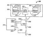
- Memory systems 300 and 305include a controller 310 , a plurality of point-to-point links 320 a – 320 n , and a plurality of memory subsystems 330 a – 330 n .
- memory subsystem 330 aa more detailed embodiment of memory subsystem 330 a is illustrated as memory subsystem 340 .
- Buffer device 350 and a plurality of memory devices 360are disposed on memory subsystem 340 .
- Buffer device 350is coupled to the plurality of memory devices 360 via channels 370 .
- Interface 375 disposed on controller 310includes a plurality of memory subsystem ports 378 a – 378 n .
- a “port”is a portion of an interface that serves a congruent I/O functionality.
- One of memory subsystem ports 378 a – 378 nincludes I/Os, for sending and receiving data, addressing and control information over one of point-to-point links 320 a – 320 n.
- At least one memory subsystemis connected to one memory subsystem port via one point-to-point link.
- the memory subsystem portis disposed on the memory controller interface which includes a plurality of memory subsystem ports, each having a connection to a point-to-point link.
- point-to-point links 320 a – 320 nare incorporated on a common substrate (not shown) such as a wafer or a printed circuit board (PCB) in memory system 300 .
- memory subsystemsare incorporated onto individual substrates (e.g., PCBs) that are incorporated fixedly attached to a single substrate that incorporates point-to-point links 320 a – 320 n and controller 310 .
- FIG. 3Apoint-to-point links 320 a – 320 n , memory subsystems 330 a – 330 c , and controller 310 , are incorporated on a common substrate (not shown) such as a wafer or a printed circuit board (PCB) in memory system 300 .
- memory subsystemsare incorporated onto individual substrates (e.g., PCBs) that are incorporated fixedly attached to a single substrate that incorporates point-to-point links 320 a – 320 n and controller 310 .
- memory subsystems 330 a – 330 care incorporated onto individual substrates which include connectors 390 a – 390 c to support upgradeability in memory system 305 .
- Corresponding mating connectors 380 a – 380 nare connected to a connection point of each point-to-point link 320 a – 320 n .
- Each of mating connectors 380 a – 380 ninterface with connectors 390 a – 390 c to allow removal/inclusion of memory subsystems 330 a – 330 c in memory system 305 .
- mating connectors 380 a – 380 nare sockets and connectors 390 a – 390 c are edge connectors disposed on an edge of each substrate 330 a – 330 c .
- Mating connectors 380 a – 380 nare attached to a common substrate shared with point-to-point connections 320 a – 320 n and controller 310 .
- buffer device 350transceives and provides isolation between signals interfacing to controller 310 and signals interfacing to the plurality of memory devices 360 .
- buffer device 350receives control, and address information from controller 310 via point-to-point link 320 a and in response, transmits corresponding signals to one or more, or all of memory devices 360 via channel 370 .
- One or more of memory devices 360may respond by transmitting data to Buffer device 350 which receives the data via one or more of channels 370 and in response, transmits corresponding signals to controller 310 via point-to-point link 320 a .
- Controller 310receives the signals corresponding to the data at corresponding port 378 a – 378 n .
- memory subsystems 330 a – 330 nare buffered modules.
- buffers disposed on the conventional DIMM module in U.S. Pat. No. 5,513,135are employed to buffer or register control signals such as RAS, and CAS, etc., and address signals.
- Data I/Os of the memory devices disposed on the DIMMare connected directly to the DIMM connector (and ultimately to data lines on an external bus when the DIMM is employed in memory system 100 ).
- Buffer device 350provides a high degree of system flexibility. New generations of memory devices may be phased in with controller 310 or into memory system 300 by modifying buffer device 350 . Backward compatibility with existing generations of memory devices (i.e., memory devices 360 ) may also be preserved. Similarly, new generations of controllers may be phased in which exploit features of new generations of memory devices while retaining backward compatibility with existing generations of memory devices.
- Buffer device 350effectively reduces the number of loading permutations on the corresponding point-to-point link to one, thus simplifying test procedures.
- characterization of a point to point linkmay involve aspects such as transmitters and receivers at opposite ends, few to no impedance discontinuities, and relatively short interconnects.
- characterization of control/address bus 130may involve aspects such as multiple transmit and receive points, long stub lines, and multiple load configurations, to name a few.
- the increased number of electrical permutationstend to add more complexity to the design, test, verification and validation of memory system 100 .
- Buffered modules added to upgrade memory system 300are accommodated by independent point-to-point links. Relative to a bussed approach, system level design, verification and validation considerations are reduced, due to the decreased amount of module inter-dependence provided by the independent point-to-point links. Additionally, the implementation, verification and validation of buffered modules may be performed with less reliance on system level environment factors.
- point-to-point links 320 a – 320 ninclude a plurality of link architectures, signaling options, clocking options and interconnect types.
- Embodiments having different link architecturesinclude simultaneous bi-directional links, time-multiplexed bi-directional links and multiple unidirectional links.
- Voltage or current mode signalingmay be employed in any of these link architectures.
- Clocking methodsinclude any of globally synchronous clocking; source synchronous clocking (i.e., where data is transported alongside the clock) and encoding the data and the clock together.
- differential signalingis employed and is transported over differential pair lines.
- one or more common voltage or current referencesare employed with respective one or more current/voltage mode level signaling.
- multi-level signaling-where information is transferred using symbols formed from multiple signal (i.e., voltage/current) levelsis employed.
- Signaling over point-to-point links 320 a – 320 nmay incorporate different modulation methods such as non-return to zero (NRZ), multi-level pulse amplitude modulation (PAM), phase shift keying, delay or time modulation, quadrature amplitude modulation (QAM) and Trellis coding.
- modulation methodssuch as non-return to zero (NRZ), multi-level pulse amplitude modulation (PAM), phase shift keying, delay or time modulation, quadrature amplitude modulation (QAM) and Trellis coding.
- Other signaling methods and apparatusmay be employed in point-to-point links 320 a – 320 n , for example, optical fiber based apparatus and methods.
- point-to-point linkdenotes one or a plurality of signal lines, each signal line having only two transceiver connection points, each transceiver connection point coupled to transmitter circuitry, receiver circuitry or transceiver circuitry.
- a point-to-point linkmay include a transmitter coupled at or near one end and a receiver coupled at or near the other end.
- the point-to-point linkmay be synonymous and interchangeable with a point-to-point connection or a point-to-point coupling.
- the number of transceiver points along a signal linedistinguishes between a point-to-point link and a bus.
- the point-to-point linkconsists of two transceiver connection points while a bus consists of more than two transceiver points.
- One or more terminatorsmay terminate each signal line in point-to-point links 320 a – 320 n .
- the terminatorsare connected to the point-to-point link and situated on buffer device 350 , on a memory module substrate and optionally on controller 310 at memory subsystem ports 378 a – 378 n .
- the terminator(s)connect to a termination voltage, such as ground or a reference voltage.
- the terminatormay be matched to the impedance of each transmission line in point-to-point links 320 a – 320 n , to help reduce voltage reflections.
- the data ratemay be increased without increasing either the system clock frequency or the number of signal lines by employing multiple voltage levels to encode unique sets of consecutive digital values or symbols. That is, each unique combination of consecutive digital symbols may be assigned to a unique voltage level, or pattern of voltage levels.
- a 4-level PAM schememay employ four distinct voltage ranges to distinguish between a pair of consecutive digital values or symbols such as 00, 01, 10 and 11. Here, each voltage range would correspond to one of the unique pairs of consecutive symbols.
- Modules 400 and 405include buffer device 405 and a plurality of memory devices 410 a – 410 h communicating over a pair of channels 415 a and 415 b .
- channel 415 acommunicates to memory devices 410 a – 410 d
- channel 415 bcommunicates to memory devices 410 e – 410 h.
- channels 415 a and 415 bconsist of a plurality of signal lines in a relatively short multi-drop bus implementation.
- the plurality of signal linesmay be controlled impedance transmission lines that are terminated using respective termination elements 420 a and 420 b .
- Channels 415 a and 415 bare relatively short (i.e., are coupled to relatively few memory devices relative to a conventional memory system, for example see FIGS. 2A and 2B ) and connect to an I/O interface (not shown) of each memory device via a short stub.
- Signal lines of channels 415 a and 415 binclude control lines (RQ), data lines (DQ) and clock lines (CFM, CTM).
- control linestransport control (e.g., read, write, precharge . . . ) information and address (e.g., row and column) information contained in packets.
- control linestransport control (e.g., read, write, precharge . . . ) information and address (e.g., row and column) information contained in packets.
- control linesmay comprise individual control lines, for example, row address strobe, column address strobe, etc., and address lines.
- Individual point-to-point control and address linesincrease the number of parallel signal connection paths, thereby increasing system layout resource requirements with respect to a narrow “packet protocol” approach.
- individual device select lines 633 a and 633 bare employed to perform device selection. Individual device select lines 633 a and 633 b decrease some latency consumed by decoding device identification which normally is utilized when multiple devices share the same channel and incorporate individual device identification values.
- Clock lines of channels 415 a and 415 binclude a terminated clock-to-master (CTM) (i.e., clock to buffer) and clock-from-master (CFM) (i.e., clock from buffer) line.
- CTMmay be transition or edge aligned with control and/or data communicated to buffer device 405 from one or more of memory devices 410 a– 410 d in, for example, a read operation.
- CFMmay be aligned with or used to synchronize control and/or data from the buffer to memory in, for example, a write operation.
- FIG. 4Aillustrates a quad-channel module 450 having channels 415 a – 415 d .
- channels 415 c and 415 dare routed in parallel with channels 415 a and 415 b to support more memory devices (e.g., 32 memory devices).
- channels 415 a and 415 bmay operate simultaneously with channels 415 c and 415 d to realize greater bandwidth.
- the bandwidth of the modulemay be increased independently of the memory capacity.
- the advantages of greater bandwidthmay be realized in conjunction with larger capacity as more modules incorporated the memory system 305 (see FIG. 3B ) increase the system memory capacity.
- the modulesare double sided and channels along with corresponding pluralities of memory devices are implemented on both sides. Using both sides of the module increases capacity or increases bandwidth without impacting module height. Both capacity and bandwidth may increase using this approach. Indeed, these techniques may increase capacity and bandwidth singly or in combination.
- modules 410 i and 410 r intended for ECCare disposed on module 470 .
- memory devices 410 a – 410 hare Rambus Dynamic Random access Memory (RDRAM) devices operating at a data rate of 1066 Mbits/sec.
- Other memory devicesmay be implemented on module 400 , for example, Double Data Rate (DDR) DRAM devices and Synchronous DRAM (SDRAM) devices.
- Utilizing buffer device 405 between the memory devices and controller in accordance with the present inventionmay feasibly render the type of memory device transparent to the system.
- Different types of memory devicesmay be included on different modules within a memory system, by employing buffer device 405 to translate protocols employed by controller 310 to the protocol utilized in a particular memory device implementation.
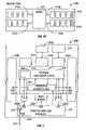
- Buffer device 405includes interface 510 , interface 520 a and 520 b , multiplexing 530 a and 530 b , control logic 540 , write buffer 550 , optional cache 560 , computation block 565 , clock circuitry 570 and operations circuitry 572 .
- interface 510couples to external point-to-point link 320 (e.g., point-to-point links 320 a – 320 n in FIGS. 3A and 3B ).
- Interface 510includes a port having transceiver 575 (i.e. transmit and receive circuitry) that connects to a point-to-point link.
- Point-to-point link 320comprises one or a plurality of signal lines, each signal line having no more than two transceiver connection points.
- One of the two transceiver connection pointsis included on interface 510 .
- Buffer device 405may include additional ports to couple additional point-to-point links between buffer device 405 and other buffer devices on other memory modules. These additional ports may be employed to expand memory capacity as is described in more detail below.
- buffer device 405may function as a transceiver between point-to-point link 320 and other point-to-point links.
- termination 580is disposed on buffer device 405 and is connected to transceiver 575 and point-to-point link 320 .
- transceiver 575includes an output driver and a receiver.
- Termination 580may dissipate signal energy reflected (i.e., a voltage reflection) from transceiver 575 .
- Termination 580may be a resistor or capacitor or inductor, singly or a series/parallel combination thereof.
- termination 580may be external to buffer device 405 .
- termination 580may be disposed on a module substrate or on a memory system substrate.
- signal energy reflected from transceiver 575may be utilized in a constructive manner according to an embodiment.
- a reflected waveformis summed with an incident waveform to achieve a greater signal amplitude.
- layout spacemay be saved by eliminating termination 580 .
- System powermay also be saved using this approach since smaller incident voltage amplitude waveforms may be employed.
- This approachmay be equally applicable to the transceiver end of the point-to-point link, or to channels 415 a and 415 b (see FIGS. 4A to 4C ).
- interfaces 520 a and 520 breceive and transmit to memory devices disposed on the module (e.g., see FIGS. 4A , 4 B and 4 C) via channels. Ports included on interfaces 520 a and 520 b connect to each channel. In alternate embodiments of the present invention, interfaces 520 a and 520 b include any number of channels e.g., two, four, eight or more channels.
- multiplexers 530 a and 530 bperform bandwidth-concentrating operations, between interface 510 and interfaces 520 a and 520 b .
- the concept of bandwidth concentrationinvolves combining the (smaller) bandwidth of each channel in a multiple channel embodiment to match the (higher) overall bandwidth utilized in a smaller group of channels. This approach typically utilizes multiplexing and demultiplexing of throughput between the multiple channels and smaller group of channels.
- buffer device 405utilizes the combined bandwidth of interfaces 520 a and 520 b to match the bandwidth of interface 510 . Bandwidth concentration is described in more detail below.
- Cache 560is one performance enhancing feature that may be incorporated onto buffer device 405 .
- Employing a cache 560may improve memory access time by providing storage of most frequently referenced data and associated tag addresses with lower access latency characteristics than those of the memory devices.
- Computation block 565may include a processor or controller unit, a compression/decompression engine, etc, to further enhance the performance and/or functionality of the buffer device.
- write buffer 550may improve interfacing efficiency by utilizing available data transport windows over point-to-point link 320 to receive write data and optional address/mask information. Once received, this information is temporarily stored in write buffer 550 until it is ready to be transferred to at least one memory device over interfaces 520 a and 520 b.
- a serial interface 574may be employed to couple signals utilized in initialization of module or memory device identification values, test function, set/reset, access latency values, vendor specific functions or calibration.
- Operations circuitry 572may include registers or a read-only memory (ROM) to store special information (e.g., vendor or configuration information) that may be used by the controller.
- ROMread-only memory
- Operations circuitrymay reduce costs by eliminating the need for separate devices on the module conventionally provided to perform these features (e.g., serial presence detect (SPD) employed in some conventional DIMM modules).
- SPDserial presence detect
- sideband signalsare employed to handle special functions such as reset, initialization and power management functions.
- Sideband signalsare connected via serial interface 574 and are independent from point-to-point link 320 for handling the special functions.
- sideband signalsare independently coupled to memory devices 410 a – 410 h to directly promote initialization, reset, power-up or other functionality independently of buffer device 405 .
- Other interconnect topologies of sideband signalsare possible.
- sideband signalsmay be daisy chained between buffer devices and coupled to the memory controller or daisy chained between all memory devices to the memory controller.
- dedicated sideband signalsmay be employed throughout.
- Clock circuitry 570may include clock generator circuitry (e.g., Direct Rambus Clock Generator) which may be incorporated onto buffer device 405 and thus may eliminate the need for a separate clock generating device.
- clock generator circuitrye.g., Direct Rambus Clock Generator
- module or system costsmay be decreased since the need for a unique clock generator device on the module or in the system may be eliminated. Since reliability to provide adequate clocking on an external device is eliminated, complexity is reduced since the clock may be generated on the buffer device 570 .
- PLLphase lock loop
- clocking circuitry 570includes one or more clock alignment circuits for phase or delay adjusting internal clock signals with respect to an external clock (not shown).
- Clock alignment circuitrymay utilize an external clock from an existing clock generator, or an internal clock generator to provide an internal clock, to generate internal synchronizing clock signals having a predetermined temporal relationship.
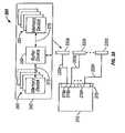
- Memory system 600includes modules 400 a and 400 b , controller 610 , and populated primary point-to-point links 620 a and 620 b .
- Unpopulated primary point-to-point links 630are populated by coupling additional modules (not shown) thereto.
- the additional modulesmay be provided to upgrade memory system 600 .
- Connectorsmay be disposed at an end of each primary point-to-point link to allow insertion or removal of the additional modules.
- Modules 400 a and 400 bmay also be provided with a connector or may be fixedly disposed (i.e., soldered) in memory system 600 .
- any number of primary point-to-point linksmay be disposed in memory system 600 , for example, three primary point-to-point links 400 a – 400 c , as shown in FIG. 6B .
- FIG. 7 and FIG. 4Ba block diagram of a memory system employing a buffered quad-channel module according to an embodiment of the present invention is illustrated.
- Memory systems 700incorporate quad-channel modules 450 a – 450 d , each coupled via point-to-point links 620 a – 620 d respectively.
- buffer device 405may operate in a bandwidth concentrator approach.
- bandwidth in each modulemay be concentrated from all quad channels 415 a – 415 d on each module to corresponding point-to-point links 620 a – 620 d .
- throughput on each of point-to-point links 620 a – 620 dis concentrated to four times the throughput achieved on each of quad channels 415 a – 415 d .
- each of channels 415 a – 415 dtransfers information between one or more respective memory devices on each channel and buffer device 405 simultaneously.
- channels 415 a – 415 dmay transfer information simultaneously and the memory devices on the other two channels 415 a and 415 b remain in a ready or standby state until called upon to perform memory access operations.
- Different applicationsmay have different processing throughput requirements.
- the throughput requirements of a particular applicationmay dynamically change during processing. Typically, more power is consumed as throughput is increased as power consumption relates in proportion to operation frequency. The amount of throughput in a system may be implemented on a dynamic throughput requirement basis to save on power consumption.
- memory system 700may concentrate bandwidth as it is required while in operation.
- memory system 700may employ only one of channels 415 a – 415 d and match throughput to the corresponding point-to-point link. As bandwidth requirements increase, memory system 700 may dynamically activate more of channels 415 a – 415 d and increase the throughput on the point-to-point link along with the number of channels accordingly to meet the bandwidth requirements for a given operation.
- Memory system 900includes modules 470 a – 470 p , coupled to controller 610 via repeaters 910 a – 910 d , primary links 920 a – 920 d , and repeater links 930 a – 930 p .
- Primary links 920 a – 920 dprovide a point to point link between controller 610 and a respective repeater 910 a – 910 d .
- each of repeaters 910 a – 910 ddecode packets transmitted from controller 610 which are then directed over one or more, or none of repeater links 930 a–d , depending the type of access required.
- Each repeater link 930 a – 930 pmay utilize a point-to-point link configuration.
- repeated links 930 a – 930 p and repeaters 910 a – 910 da larger number of modules may be accessed and a larger capacity memory system may be realized. Such a large capacity may be suited in a computer server system.
- FIG. 8Billustrates another approach utilized to expand the memory capacity of a memory system in accordance to yet another embodiment.
- a plurality of buffered modules 950 a – 950 dare “daisy chained” via a plurality of point-to-point links 960 a – 960 d to increase the overall memory capacity. Connection points of each point-to-point link are connected to two adjacent buffered modules.
- Each of buffered modules 950 a – 950 ctransceive signals between adjacent point-to-point links 960 a – 960 d .
- Point-to-point link 960 amay be coupled to a controller or another buffered module.
- Additional point-to-point linksmay be coupled to a buffer device in a tree configuration approach.
- three point-to-point links 970 a – 970 c each having a single end connected to one buffer devicemay be employed as shown in FIG. 8C .
Landscapes
- Engineering & Computer Science (AREA)
- Theoretical Computer Science (AREA)
- Physics & Mathematics (AREA)
- General Engineering & Computer Science (AREA)
- General Physics & Mathematics (AREA)
- Dram (AREA)
Abstract
Description
This is a continuation of U.S. patent application Ser. No. 10/952,667 filed on Sep. 28, 2004 (still pending); which is a continuation of U.S. patent application Ser. No. 10/625,276 filed on Jul. 23, 2003 (now U.S. Pat. No. 6,832,284); which is a continuation of U.S. patent application Ser. No. 10/272,024 filed on Oct. 15, 2002 (still pending); which is a continuation of application Ser. No. 09/479,375 filed on Jan. 5, 2000 (now U.S. Pat. No. 6,502,161).
This invention relates to memory systems, memory subsystems, memory modules or a system having memory devices. More specifically, this invention is directed toward memory system architectures which may include integrated circuit devices such as one or more controllers and a plurality of memory devices.
Some contemporary memory system architectures may demonstrate tradeoffs between cost, performance and the ability to upgrade, for example; the total memory capacity of the system. Memory capacity is commonly upgraded via memory modules or cards featuring a connector/socket interface. Often these memory modules are connected to a bus disposed on a backplane to utilize system resources efficiently. System resources include integrated circuit die area, package pins, signal line traces, connectors, backplane board area, just to name a few. In addition to upgradeability, many of these contemporary memory systems also require high throughput for bandwidth intensive applications, such as graphics.
With reference toFIG. 1 , a representational block diagram of a conventional memory system employing memory modules is illustrated.Memory system 100 includesmemory controller 110 and modules120a–120c.Memory controller 110 is coupled to modules120a–120cvia control/address bus 130,data bus 140, and correspondingmodule control lines 150a–150c. Control/address bus 130 typically comprises a plurality of address lines and control signals (e.g., RAS, CAS and WE).
The address lines and control signals of control/address bus 130 are bussed and “shared” between each of modules120a–120cto provide row/column addressing and read/write, precharge, refresh commands, etc., to memory devices on a selected one of modules120a–120c. Individualmodule control lines 150a–150care typically dedicated to a corresponding one of modules120a–120cto select which of modules120a–120cmay utilize the control/address bus 130 anddata bus 140 in a memory operation.
Here and in the detailed description to follow, “bus” denotes a plurality of signal lines, each having more than two connection points for “transceiving” (i.e., transmitting or receiving). Each connection point electrically connects or couples to a transceiver (i.e., a transmitter-receiver) or one of a single transmitter or receiver circuit.
With further reference toFIG. 1 ,memory system 100 may provide an upgrade path through the usage of modules120a–120c. A socket and connector interface may be employed which allows each module to be removed and replaced by a memory module that is faster or includes a higher capacity.Memory system 100 may be configured with unpopulated sockets or less than a full capacity of modules (i.e., empty sockets/connectors) and provided for increased capacity at a later time with memory expansion modules. Since providing a separate group of signals (e.g., address lines and data lines) to each module is avoided using the bussed approach, system resources inmemory system 100 are efficiently utilized.
U.S. Pat. No. 5,513,135 discloses a contemporary dual inline memory module (DIMM) having one or more discrete buffer devices. In this patent, the discrete buffer devices are employed to buffer or register signals between memory devices disposed on the module and external bussing (such as control/address bus 130 in memory system100). The discrete buffer devices buffer or register incoming control signals such as RAS, and CAS, etc., and address signals. Local control/address lines are disposed on the contemporary memory module to locally distribute the buffered or registered control and address signals to each memory device on the module. By way of note, the discrete buffer devices buffer a subset of all of the signals on the memory module since data path signals (e.g.,data bus 140 inFIG. 1 ) of each memory device are connected directly to the external bus.
In addition to the discrete buffer device(s), a phase locked Loop (PLL) device may be disposed on the contemporary DIMM described above. The PLL device receives an external clock and generates a local phase adjusted clock for each memory device as well as the discrete buffer devices.
Modules such as the DIMM example disclosed in U.S. Pat. No. 5,513,135 feature routed connections between input/outputs (I/Os) of each memory device and connector pads disposed at the edge of the module substrate. These routed connections introduce long stub lines between the signal lines of the bus located off of the module (e.g.,control address bus 130 and data bus140), and memory device I/Os. A stub line is commonly known as a routed connection that deviates from the primary path of a signal line. Stub lines commonly introduce impedance discontinuities to the signal line. Impedance discontinuities may produce undesirable voltage reflections manifested as signal noise that may ultimately limit system operating frequency.
Examples of contemporary memory systems employing buffered modules are illustrated inFIGS. 2A and 2B .FIG. 2A illustrates amemory system 200 based on a Rambus™ channel architecture andFIG. 2B illustrates amemory system 210 based on a Synchronous Link architecture. Both of these systems feature memory modules havingbuffer devices 250 disposed along multiple transmit/receive connection points ofbus 260. In both of these examples, the lengths of stubs are significantly shortened in an attempt to minimize signal reflections and enable higher bandwidth characteristics. Ultimately however, memory configurations such as the ones portrayed bymemory systems
In the bussed approach exemplified inFIGS. 1 ,2A and2B, the signal lines of the bussed signals become loaded with a (load) capacitance associated with each bus connection point. These load capacitances are normally attributed to components of input/output (I/O) structures disposed on an integrated circuit (IC) device, such as a memory device or buffer device. For example, bond pads, electrostatic discharge devices, input buffer transistor capacitance, and output driver transistor parasitic and interconnect capacitances relative to the IC device substrate all contribute to the memory device load capacitance.
The load capacitances connected to multiple points along the length of the signal line may degrade signaling performance. As more load capacitances are introduced along the signal line of the bus, signal settling time correspondingly increases, reducing the bandwidth of the memory system. In addition, impedance along the signal line may become harder to control or match as more load capacitances are present along the signal line. Mismatched impedance may introduce voltage reflections that cause signal detection errors. Thus, for at least these reasons, increasing the number of loads along the bus imposes a compromise to the bandwidth of the memory system.
In an upgradeable memory system, such asconventional memory system 100, different memory capacity configurations become possible. Each different memory capacity configuration may present different electrical characteristics to the control/address bus 130. For example, load capacitance along each signal line of the control/address bus 130 may change with two different module capacity configurations.
As memory systems incorporate an increasing number of memory module configurations, the verification and validation of the number of permutations that these systems make possible may become increasingly more time consuming. Verification involves the confirmation of operation, logical and/or physical functionality of an IC by running tests on models of the memory, associated devices and/or bus prior to manufacturing the device. Validation involves testing the assembled system or components thereof (e.g., a memory module). Validation typically must account for a majority of the combinations or permutations of system conditions and possibilities which different memory configurations (e.g., 256 Mbyte, 1 Gbyte . . . ) present including signaling, electrical characteristics (e.g., impedance, capacitance, and inductance variations), temperature effects, different operating frequencies, different vendor interfaces, etc, to name a few. Thus, as the number of possible memory configurations increase, the test and verification time required also increases. More time required to test a system often increases the cost of bringing the system to market or delays a product introduction beyond an acceptable window of time to achieve competitiveness.
There is a need for memory system architectures or interconnect topologies that provide cost effective upgrade capabilities without compromising bandwidth. Using conventional signaling schemes, the bussed approaches lend efficiency towards resource utilization of a system and permits module interfacing for upgradeability. However, the bussed approach may suffer from bandwidth limitations that stem from the electrical characteristics inherent in the bus topology. In addition, impedance along a signal line may be increasingly more difficult to control with increased connection points along a signal line, introducing impedance mismatch and signal reflections. Utilizing the bussed approach in implementing an upgradeable memory system introduces many possible electrical permutations and combinations with each unique module configuration.
The present invention is directed toward memory system architectures (i.e., interconnect topologies) which include a controller communicating to at least one memory subsystem (e.g., a buffered memory module). An independent point-to-point link may be utilized between the controller and each memory subsystem to eliminate physical inter-dependence between memory subsystems. According to an embodiment, the memory system may be upgraded by coupling additional memory module(s), each via a dedicated point-to-point link to the controller. Bandwidth may scale upwards as the memory system is upgraded by the additional memory module(s).
In one aspect, the present invention is a memory system comprising a memory controller having an interface and at least a first memory subsystem. The interface includes a plurality of memory subsystem ports including a first memory subsystem port. The first memory subsystem includes a buffer device having a first port and a second port, and a plurality of memory devices coupled to the buffer device via the second port. A plurality of point-to-point links include a first point-to-point link. Each point-to-point link has a connection to a respective memory subsystem port of the plurality of memory subsystem ports. The first point-to-point link connecting the first port to a first memory subsystem port to transfer data between the plurality of memory devices and the memory controller.
In another aspect, the present invention is a memory system comprising a controller device and first and second buffer devices, each having a first interface and a second interface. A first point-to-point link includes a first connection to the controller device and a second connection to the first interface of the first buffer device. A first channel is connected to the second interface of the first buffer device, and a first plurality of memory devices are electrically coupled to the first channel. A second point-to-point link includes a first connection to the controller device and a second connection to the first interface of the second buffer. A second channel is connected to the second interface of the second buffer device, and a second plurality of memory devices are electrically coupled to the second channel.
In yet another aspect, the present invention comprises a controller device, and a first and second plurality of buffer devices, each buffer device having a first interface connected to a plurality of memory devices. First and second point-to-point links each include a first end connected to the controller device and a second end connected to a repeater device. A plurality of repeater links couple the first and second repeater devices to respective first and second pluralities of buffer devices.
In another aspect the present invention is a memory system comprising a controller device; a first, second and third connectors; and first second and third point-to-point links. Each of the respective first, second point-to-point links includes a first connection to the interface and a second connection to the respective first, second and third connectors. In this aspect the present invention also includes a first memory subsystem having a buffer device and a plurality of memory devices. The buffer device includes a first interface connected to the first connector, and a second interface connected to the plurality of memory devices. The second and third connectors may support coupling to respective second and third memory subsystems.
The present invention is described in the detailed description, including the embodiments to follow. The detailed description and embodiments are given by way of illustration only. The scope of the invention is defined by the attached claims. Various modifications to the embodiments of the present invention remain within the scope defined by the attached claims.
In the course of the detailed description to follow, reference will be made to the attached drawings, in which:
The present invention relates to a memory system which includes a plurality of point-to-point links connected to a master. At least one point-to-point link connects at least one memory subsystem to the master, (e.g., a processor or controller). The memory system may be upgraded by coupling memory subsystems to the master via respective dedicated point-to-point links. Each memory subsystem includes a buffer device that communicates to a plurality of memory devices. The master communicates with each buffer device via each point-to-point link. The buffer device may be disposed on a memory module along with the plurality of memory devices and connected to the point-to-point link via a connector. Alternatively, the buffer device may be disposed on a common printed circuit board or backplane link along with the corresponding point-to-point link and master.
“Memory devices” are a common class of integrated circuit devices that have an array of memory cells, such as, dynamic random access memory (DRAM), static random access memory (SRAM), etc. A “memory subsystem” is a plurality of memory devices interconnected with an integrated circuit device (e.g., a buffer device) providing access between the memory devices and an overall system, for example, a computer system. It should be noted that a memory system is distinct from a memory subsystem in that a memory system may include one or more memory subsystems. A “memory module” or simply just “module” denotes a substrate having a plurality of memory devices employed with a connector interface. It follows from these definitions that a memory module having a buffer device isolating data, control, and address signals of the memory devices from the connector interface is a memory subsystem.
With reference toFIGS. 3A and 3B , block diagrams of a memory system according to embodiments of the present invention are illustrated.Memory systems controller 310, a plurality of point-to-point links 320a–320n, and a plurality ofmemory subsystems 330a–330n. For simplicity, a more detailed embodiment ofmemory subsystem 330ais illustrated asmemory subsystem 340.Buffer device 350 and a plurality ofmemory devices 360 are disposed onmemory subsystem 340.Buffer device 350 is coupled to the plurality ofmemory devices 360 viachannels 370.Interface 375 disposed oncontroller 310 includes a plurality ofmemory subsystem ports 378a–378n. A “port” is a portion of an interface that serves a congruent I/O functionality. One ofmemory subsystem ports 378a–378nincludes I/Os, for sending and receiving data, addressing and control information over one of point-to-point links 320a–320n.
According to an embodiment of the present invention, at least one memory subsystem is connected to one memory subsystem port via one point-to-point link. The memory subsystem port is disposed on the memory controller interface which includes a plurality of memory subsystem ports, each having a connection to a point-to-point link.
InFIG. 3A , point-to-point links 320a–320n,memory subsystems 330a–330c, andcontroller 310, are incorporated on a common substrate (not shown) such as a wafer or a printed circuit board (PCB) inmemory system 300. In an alternate embodiment, memory subsystems are incorporated onto individual substrates (e.g., PCBs) that are incorporated fixedly attached to a single substrate that incorporates point-to-point links 320a–320nandcontroller 310. In another alternate embodiment illustrated inFIG. 3B ,memory subsystems 330a–330care incorporated onto individual substrates which include connectors390a–390cto support upgradeability inmemory system 305. Correspondingmating connectors 380a–380nare connected to a connection point of each point-to-point link 320a–320n. Each ofmating connectors 380a–380ninterface with connectors390a–390cto allow removal/inclusion ofmemory subsystems 330a–330cinmemory system 305. In one embodiment,mating connectors 380a–380nare sockets and connectors390a–390care edge connectors disposed on an edge of eachsubstrate 330a–330c.Mating connectors 380a–380n, are attached to a common substrate shared with point-to-point connections 320a–320nandcontroller 310.
With further reference toFIGS. 3A and 3B ,buffer device 350 transceives and provides isolation between signals interfacing tocontroller 310 and signals interfacing to the plurality ofmemory devices 360. In a normal memory read operation,buffer device 350 receives control, and address information fromcontroller 310 via point-to-point link 320aand in response, transmits corresponding signals to one or more, or all ofmemory devices 360 viachannel 370. One or more ofmemory devices 360 may respond by transmitting data to Bufferdevice 350 which receives the data via one or more ofchannels 370 and in response, transmits corresponding signals tocontroller 310 via point-to-point link 320a.Controller 310 receives the signals corresponding to the data at correspondingport 378a–378n. In this embodiment,memory subsystems 330a–330nare buffered modules. By way of comparison, buffers disposed on the conventional DIMM module in U.S. Pat. No. 5,513,135 are employed to buffer or register control signals such as RAS, and CAS, etc., and address signals. Data I/Os of the memory devices disposed on the DIMM are connected directly to the DIMM connector (and ultimately to data lines on an external bus when the DIMM is employed in memory system100).
Buffered modules added to upgrade memory system300 (e.g., increase memory capacity) are accommodated by independent point-to-point links. Relative to a bussed approach, system level design, verification and validation considerations are reduced, due to the decreased amount of module inter-dependence provided by the independent point-to-point links. Additionally, the implementation, verification and validation of buffered modules may be performed with less reliance on system level environment factors.
Several embodiments of point-to-point links 320a–320ninclude a plurality of link architectures, signaling options, clocking options and interconnect types. Embodiments having different link architectures include simultaneous bi-directional links, time-multiplexed bi-directional links and multiple unidirectional links. Voltage or current mode signaling may be employed in any of these link architectures. Clocking methods include any of globally synchronous clocking; source synchronous clocking (i.e., where data is transported alongside the clock) and encoding the data and the clock together. In one embodiment, differential signaling is employed and is transported over differential pair lines. In alternate embodiments, one or more common voltage or current references are employed with respective one or more current/voltage mode level signaling. In yet other embodiments, multi-level signaling-where information is transferred using symbols formed from multiple signal (i.e., voltage/current) levels is employed.
Signaling over point-to-point links 320a–320nmay incorporate different modulation methods such as non-return to zero (NRZ), multi-level pulse amplitude modulation (PAM), phase shift keying, delay or time modulation, quadrature amplitude modulation (QAM) and Trellis coding. Other signaling methods and apparatus may be employed in point-to-point links 320a–320n, for example, optical fiber based apparatus and methods.
The term “point-to-point link” denotes one or a plurality of signal lines, each signal line having only two transceiver connection points, each transceiver connection point coupled to transmitter circuitry, receiver circuitry or transceiver circuitry. For example, a point-to-point link may include a transmitter coupled at or near one end and a receiver coupled at or near the other end. The point-to-point link may be synonymous and interchangeable with a point-to-point connection or a point-to-point coupling.
In keeping with the above description, the number of transceiver points along a signal line distinguishes between a point-to-point link and a bus. According to the above, the point-to-point link consists of two transceiver connection points while a bus consists of more than two transceiver points.
One or more terminators (e.g., a resistive element) may terminate each signal line in point-to-point links 320a–320n. In several embodiments of the present invention, the terminators are connected to the point-to-point link and situated onbuffer device 350, on a memory module substrate and optionally oncontroller 310 atmemory subsystem ports 378a–378n. The terminator(s) connect to a termination voltage, such as ground or a reference voltage. The terminator may be matched to the impedance of each transmission line in point-to-point links 320a–320n, to help reduce voltage reflections.
In an embodiment of the present invention employing multi-level PAM signaling, the data rate may be increased without increasing either the system clock frequency or the number of signal lines by employing multiple voltage levels to encode unique sets of consecutive digital values or symbols. That is, each unique combination of consecutive digital symbols may be assigned to a unique voltage level, or pattern of voltage levels. For example, a 4-level PAM scheme may employ four distinct voltage ranges to distinguish between a pair of consecutive digital values or symbols such as 00, 01, 10 and 11. Here, each voltage range would correspond to one of the unique pairs of consecutive symbols.
With reference toFIGS. 4A ,4B and4C, buffered memory modules according to embodiments of the present invention are shown.Modules buffer device 405 and a plurality ofmemory devices 410a–410hcommunicating over a pair ofchannels memory devices 410a–410dandchannel 415bcommunicates tomemory devices 410e–410h.
In an embodiment,channels respective termination elements Channels FIGS. 2A and 2B ) and connect to an I/O interface (not shown) of each memory device via a short stub. Signal lines ofchannels point links 320a–320nmay equally apply tochannels
In accordance with an embodiment of the present invention, control lines (RQ) transport control (e.g., read, write, precharge . . . ) information and address (e.g., row and column) information contained in packets. By bundling control and address information in packets, protocols required to communicate tomemory devices 410a–410hare independent of the physical control/address interface implementation.
In alternate embodiments, control lines (RQ) may comprise individual control lines, for example, row address strobe, column address strobe, etc., and address lines. Individual point-to-point control and address lines increase the number of parallel signal connection paths, thereby increasing system layout resource requirements with respect to a narrow “packet protocol” approach. In one alternate embodiment illustrated inFIG. 6A , individual deviceselect lines select lines
Clock lines ofchannels buffer device 405 from one or more ofmemory devices 410a–410din, for example, a read operation. CFM may be aligned with or used to synchronize control and/or data from the buffer to memory in, for example, a write operation.
Although twochannels FIG. 4A , a single channel is also feasible. In other embodiments, more than two channels may be incorporated ontomodule 400. It is conceivable that if each channel and memory device interface is made narrow enough, then a dedicated channel between each memory device and the buffer device may be implemented on the module. The width of the channel refers to the number of parallel signal paths included in each channel.FIG. 4B illustrates a quad-channel module 450 havingchannels 415a–415d. In this embodiment,channels channels FIG. 4B ) may be implemented in memory systems that require large memory capacity, for example, in server or workstation class systems.
In alternate embodiments,channels channels FIG. 3B ) increase the system memory capacity. In other alternate embodiments, the modules are double sided and channels along with corresponding pluralities of memory devices are implemented on both sides. Using both sides of the module increases capacity or increases bandwidth without impacting module height. Both capacity and bandwidth may increase using this approach. Indeed, these techniques may increase capacity and bandwidth singly or in combination.
Other features may also be incorporated to enhancemodule 400 in high capacity memory systems, for example, additional memory devices and interface signals for error correction code storage and transport (ECC). Referring toFIG. 4C ,memory devices module 470.
In one embodiment,memory devices 410a–410hare Rambus Dynamic Random access Memory (RDRAM) devices operating at a data rate of 1066 Mbits/sec. Other memory devices may be implemented onmodule 400, for example, Double Data Rate (DDR) DRAM devices and Synchronous DRAM (SDRAM) devices. Utilizingbuffer device 405 between the memory devices and controller in accordance with the present invention (e.g., seeFIG. 3 ) may feasibly render the type of memory device transparent to the system. Different types of memory devices may be included on different modules within a memory system, by employingbuffer device 405 to translate protocols employed bycontroller 310 to the protocol utilized in a particular memory device implementation.
With reference toFIG. 5 , a block diagram of a buffer device according to an embodiment of the present invention is illustrated.Buffer device 405 includesinterface 510,interface control logic 540, writebuffer 550,optional cache 560,computation block 565,clock circuitry 570 andoperations circuitry 572.
In an embodiment, interface510 couples to external point-to-point link320 (e.g., point-to-point links 320a–320ninFIGS. 3A and 3B ).Interface 510 includes a port having transceiver575 (i.e. transmit and receive circuitry) that connects to a point-to-point link. Point-to-point link 320 comprises one or a plurality of signal lines, each signal line having no more than two transceiver connection points. One of the two transceiver connection points is included oninterface 510.Buffer device 405 may include additional ports to couple additional point-to-point links betweenbuffer device 405 and other buffer devices on other memory modules. These additional ports may be employed to expand memory capacity as is described in more detail below. In the embodiment shown inFIG. 5 ,buffer device 405 may function as a transceiver between point-to-point link 320 and other point-to-point links.
In one embodiment,termination 580 is disposed onbuffer device 405 and is connected totransceiver 575 and point-to-point link 320. In this embodiment,transceiver 575 includes an output driver and a receiver.Termination 580 may dissipate signal energy reflected (i.e., a voltage reflection) fromtransceiver 575.Termination 580 may be a resistor or capacitor or inductor, singly or a series/parallel combination thereof. In alternate embodiments,termination 580 may be external to bufferdevice 405. For example,termination 580 may be disposed on a module substrate or on a memory system substrate.
In another approach, signal energy reflected fromtransceiver 575 may be utilized in a constructive manner according to an embodiment. By correctly placing a receive point spaced by a distance from the end of point-to-point link 320, a reflected waveform is summed with an incident waveform to achieve a greater signal amplitude. In this approach, layout space may be saved by eliminatingtermination 580. System power may also be saved using this approach since smaller incident voltage amplitude waveforms may be employed. This approach may be equally applicable to the transceiver end of the point-to-point link, or tochannels FIGS. 4A to 4C ).
With further reference toFIG. 5 ,interfaces FIGS. 4A ,4B and4C) via channels. Ports included oninterfaces
According to an embodiment of the present invention,multiplexers interface 510 andinterfaces buffer device 405 utilizes the combined bandwidth ofinterfaces interface 510. Bandwidth concentration is described in more detail below.
Aserial interface 574 may be employed to couple signals utilized in initialization of module or memory device identification values, test function, set/reset, access latency values, vendor specific functions or calibration.Operations circuitry 572 may include registers or a read-only memory (ROM) to store special information (e.g., vendor or configuration information) that may be used by the controller. Operations circuitry may reduce costs by eliminating the need for separate devices on the module conventionally provided to perform these features (e.g., serial presence detect (SPD) employed in some conventional DIMM modules).
According to an embodiment of the present invention, sideband signals are employed to handle special functions such as reset, initialization and power management functions. Sideband signals are connected viaserial interface 574 and are independent from point-to-point link 320 for handling the special functions. In other embodiments sideband signals are independently coupled tomemory devices 410a–410hto directly promote initialization, reset, power-up or other functionality independently ofbuffer device 405. Other interconnect topologies of sideband signals are possible. For example, sideband signals may be daisy chained between buffer devices and coupled to the memory controller or daisy chained between all memory devices to the memory controller. Alternatively, dedicated sideband signals may be employed throughout.
According to an embodiment of the present invention, clockingcircuitry 570 includes one or more clock alignment circuits for phase or delay adjusting internal clock signals with respect to an external clock (not shown). Clock alignment circuitry may utilize an external clock from an existing clock generator, or an internal clock generator to provide an internal clock, to generate internal synchronizing clock signals having a predetermined temporal relationship.
With reference toFIGS. 6A , and6B, block diagrams of a memory system according to embodiments of the present invention are illustrated.Memory system 600 includesmodules controller 610, and populated primary point-to-point links point links 630 are populated by coupling additional modules (not shown) thereto. The additional modules may be provided to upgradememory system 600. Connectors may be disposed at an end of each primary point-to-point link to allow insertion or removal of the additional modules.Modules memory system 600. Although only two populated primary point-to-point links are shown inFIG. 6A , any number of primary point-to-point links may be disposed inmemory system 600, for example, three primary point-to-point links 400a–400c, as shown inFIG. 6B .
With reference toFIG. 7 andFIG. 4B , a block diagram of a memory system employing a buffered quad-channel module according to an embodiment of the present invention is illustrated.Memory systems 700 incorporate quad-channel modules 450a–450d, each coupled via point-to-point links 620a–620drespectively.
Referring toFIG. 4B ,buffer device 405 may operate in a bandwidth concentrator approach. By employingquad channels 415a–415don each ofmodules 450a–450d, bandwidth in each module may be concentrated from allquad channels 415a–415don each module to corresponding point-to-point links 620a–620d. In this embodiment, throughput on each of point-to-point links 620a–620dis concentrated to four times the throughput achieved on each ofquad channels 415a–415d. Here, each ofchannels 415a–415dtransfers information between one or more respective memory devices on each channel andbuffer device 405 simultaneously.
Any number ofchannels 415a–415d, for example; twochannels channels memory system 700 may concentrate bandwidth as it is required while in operation. For example,memory system 700 may employ only one ofchannels 415a–415dand match throughput to the corresponding point-to-point link. As bandwidth requirements increase,memory system 700 may dynamically activate more ofchannels 415a–415dand increase the throughput on the point-to-point link along with the number of channels accordingly to meet the bandwidth requirements for a given operation.
With reference toFIG. 8A , a block diagram of a large capacity memory system according to an embodiment of the present invention is illustrated.Memory system 900 includesmodules 470a–470p, coupled tocontroller 610 viarepeaters 910a–910d,primary links 920a–920d, andrepeater links 930a–930p.Primary links 920a–920dprovide a point to point link betweencontroller 610 and arespective repeater 910a–910d. In an embodiment of the present invention, each ofrepeaters 910a–910ddecode packets transmitted fromcontroller 610 which are then directed over one or more, or none ofrepeater links 930a–d, depending the type of access required. Each repeater link930a–930pmay utilize a point-to-point link configuration. By incorporating, repeatedlinks 930a–930pandrepeaters 910a–910d, a larger number of modules may be accessed and a larger capacity memory system may be realized. Such a large capacity may be suited in a computer server system.
While this invention has been described in conjunction with what is presently considered the most practical embodiments, the invention is not limited to the disclosed embodiments. In the contrary, the embodiments disclosed cover various modifications that are within the scope of the invention as set forth in the following claims.
Claims (28)
1. A system comprising:
a master device;
a first integrated circuit buffer device;
a first plurality of integrated circuit memory devices coupled to the first integrated circuit buffer device;
a first plurality of signal lines coupled to the first integrated circuit buffer device and the master device, wherein the first plurality of signal lines communicate control information, address information and data from the master device to the first integrated circuit buffer device;
a second plurality of signal lines coupled to the first integrated circuit buffer device;
a second integrated circuit buffer device coupled to the second plurality of signal lines, the second integrated circuit buffer device to receive the control information, the address information and the data from the first integrated circuit buffer device over the second plurality of signal lines; and
a second plurality of integrated circuit memory devices coupled to the second integrated circuit buffer device; and
a third plurality of signal lines coupled to the first integrated circuit buffer device, the second integrated circuit buffer device and the master device, the third plurality of signal lines to communicate information from the master device, the information to initialize the first integrated circuit buffer device and the second integrated circuit buffer device.
2. The system ofclaim 1 , further comprising:
a first channel to couple a first integrated circuit memory device of the first plurality of integrated circuit memory devices to a first port of the first integrated circuit buffer device; and
a second channel to couple a second integrated circuit memory device of the first plurality of integrated circuit memory devices to a second port of the first integrated circuit buffer device.
3. The system ofclaim 2 , further comprising:
a first signal line coupled to the first integrated circuit memory device and the first integrated circuit buffer device, the first signal line to provide a first signal, wherein the first integrated circuit memory device transmits first read data over the first channel to the first port of the first integrated circuit buffer device, wherein the first read data propagates in a predetermined alignment with the first signal; and
a second signal line coupled to the second integrated circuit memory device and the first integrated circuit buffer device, the second signal line to provide a second signal, wherein the second integrated circuit memory device transmits second read data over the second channel to the second port of the first integrated circuit buffer device, wherein the second read data propagates in a predetermined alignment with the second signal.
4. The system ofclaim 3 , wherein the first integrated circuit buffer device receives the first read data and the second read data and transmits the first read data and the second read data to the master device over the first plurality of signal lines.
5. The system ofclaim 1 , further comprising a memory module substrate, wherein the first integrated circuit buffer device and the first plurality of integrated circuit memory devices are disposed on the memory module substrate, wherein the memory module substrate includes a connector interface to couple an interface of the first integrated circuit buffer device to the first plurality of signal lines, wherein the first integrated circuit buffer device provides isolation between signals interfacing to the first plurality of integrated circuit memory devices and signals received at the interface of the first integrated circuit buffer device.
6. The system ofclaim 1 , wherein the second integrated circuit buffer device comprises:
a first interface, coupled to the second plurality of signal lines, the first interface to receive the control information, the address information and the data from the first integrated circuit buffer device over the second plurality of signal lines;
a second interface, coupled to the second plurality of integrated circuit memory devices, to provide the control information, the address information and the data to at least a first integrated circuit memory device of the second plurality of integrated circuit memory devices.
7. The system ofclaim 1 , further comprising:
a first termination disposed on the master device, wherein the first termination is coupled to a first end of a signal line of the first plurality of signal lines; and
a second termination disposed on the first integrated circuit buffer device, wherein the second termination is coupled to a second end of the signal line of the first plurality of signal lines.
8. The system ofclaim 1 , wherein the first plurality of signal lines includes a first point-to-point link connected between the master device and the first integrated circuit buffer device, the second plurality of signal lines includes a second point-to-point link connected between the first integrated circuit buffer device and the second integrated circuit buffer device, and the third plurality of signal lines are independent of both the first plurality of signal lines and the second plurality of signal lines.
9. A method of operation in a memory system, wherein the memory system includes a controller device coupled to a first memory module and a second memory module, wherein the first memory module includes a first integrated circuit buffer device and a first plurality of integrated circuit memory devices coupled to the first integrated circuit buffer device, and the second memory module includes a second integrated circuit buffer device and a second plurality of integrated circuit memory devices coupled to the second integrated circuit buffer device, the method comprising:
the first integrated circuit buffer device receiving first control information, first address information and first data from the controller device over a first point-to-point link coupled to the first integrated circuit buffer device and the controller device;
the second integrated circuit buffer device receiving the first control information, the first address information and the first data from the first integrated circuit buffer device over a second point-to-point link coupled to the first integrated circuit buffer device and the second integrated circuit buffer device; and
the controller device providing information to initialize the first integrated circuit buffer device and the second integrated circuit buffer device.
10. The method ofclaim 9 , further comprising the controller device providing power management information to the first integrated circuit buffer device.
11. The method ofclaim 9 , wherein the first point-to-point link includes multiple unidirectional links such that the first integrated circuit buffer device receiving the first control information, the first address information and first data includes receiving the first control information, the first address information and the first data over a unidirectional link of the multiple unidirectional links.
12. The method ofclaim 9 , further comprising:
the first integrated circuit buffer device receiving a first signal from a first integrated circuit memory device of the first plurality of integrated circuit memory devices;
the first integrated circuit buffer device receiving read data from the first integrated circuit memory device, wherein the read data travels alongside the first signal; and
the first integrated circuit buffer device communicating the read data to the controller device over the first point-to-point link.
13. The method ofclaim 12 , wherein the first point-to-point link includes multiple unidirectional links such that the first integrated circuit buffer device communicating the read data to the controller device over the first point-to-point link includes communicating the read data over a unidirectional link of the multiple unidirectional links.
14. The method ofclaim 12 , further comprising transceiving, by the first integrated circuit buffer device, the first control information, the first address information and the first data, from a first interface of the first integrated circuit buffer device coupled to the first point-to-point link and a second interface of the first integrated circuit buffer device coupled to the second point-to-point link.
15. The method ofclaim 12 , wherein the first integrated circuit buffer device receiving first control information, first address information and first data from the controller device over the first point-to-point link includes receiving the first control information, the first address information and the first data from the controller device over the first point-to-point link using differential signals.
16. The method ofclaim 12 , wherein the first plurality of integrated circuit memory devices are double data rate dynamic random access memories.
17. The method ofclaim 12 , further comprising:
a third integrated circuit buffer device receiving second control information, second address information and second data from the controller device over a third point-to-point link coupled to the third integrated circuit buffer device and the controller device; and
the third integrated circuit buffer device transceiving the second control information, the second address information and the second data between an interface coupled to the third point-to-point link and a third plurality of integrated circuit memory devices.
18. A system comprising:
a memory controller device having an interface;
a first memory module having a first integrated circuit buffer device and a first plurality of integrated circuit memory devices coupled to the first integrated circuit buffer device;
a first point-to-point link coupled to the first integrated circuit buffer device and the interface of the memory controller device, the first point-to-point link to communicate control information, address information, and data from the memory controller to the first integrated circuit buffer device;
a second point-to-point link coupled to the first integrated circuit buffer device;
a second memory module having a second integrated circuit buffer device and a second plurality of integrated circuit memory devices coupled to the second integrated circuit buffer device, wherein the second integrated circuit buffer device is coupled to the second point-to-point link, the second point-to-point link to communicate the control information, the address information and the data from the first integrated circuit buffer device to the second integrated circuit buffer device; and
a plurality of signal lines coupled to the first integrated circuit buffer device, the second integrated circuit buffer device and the memory controller device, the plurality of signal lines to provide signals from the memory controller device to the first integrated circuit buffer device and the second integrated circuit buffer device, the signals including information to initialize the first integrated circuit buffer device and the second integrated circuit buffer device.
19. The system ofclaim 18 , wherein the plurality of signal lines communicate sideband signals to the first integrated circuit buffer device and the second integrated circuit buffer device, wherein the signals are sideband signals.
20. The system ofclaim 18 , wherein the first integrated circuit buffer device includes:
a first interface coupled to the plurality of signal lines, to receive the signals including information to initialize the first integrated circuit buffer device; and
a second interface coupled to the first point-to-point link, to receive the control information, address information, and data from the memory controller, wherein the first interface is separate from the second interface.
21. The system ofclaim 18 , wherein the plurality of signal lines includes a first signal line coupled to the memory controller device and the first integrated circuit buffer device, and a second signal line coupled to the memory controller device and the second integrated circuit buffer device.
22. The system ofclaim 18 , wherein the plurality of signal lines are daisy chained between the first integrated circuit buffer device and the second integrated circuit buffer device.
23. The system ofclaim 18 , wherein the signals include power management information and reset information.
24. The system ofclaim 18 , further comprising:
a first channel to couple a first integrated circuit memory device of the first plurality of integrated circuit memory devices to a first port of the first integrated circuit buffer device; and
a second channel to couple a second integrated circuit memory device of the first plurality of integrated circuit memory devices to a second port of the first integrated circuit buffer device.
25. The system ofclaim 24 , further comprising:
a first signal line coupled to the first integrated circuit buffer device and the first integrated circuit memory device, the first signal line to provide a first signal, wherein the first integrated circuit memory device transmits first read data over the first channel to the first port of the first integrated circuit buffer device, wherein the first read data propagates in a predetermined alignment with the first signal, wherein the first integrated circuit buffer device transmits the first read data over the first point-to-point link to the interface of the memory controller; and
a second signal line coupled to the first integrated circuit buffer device and the second integrated circuit memory device, the second signal line to provide a second signal, wherein the second integrated circuit memory device transmits second read data over the second channel to the second port of the first integrated circuit buffer device, wherein the second read data propagates in a predetermined alignment with the second signal, wherein the first integrated circuit buffer device transmits the first read data and the second read data to the memory controller device over the first point-to-point link.
26. The system ofclaim 18 , wherein the second integrated circuit buffer device comprises:
a first interface, coupled to the second point-to-point link, the first interface to receive the control information, the address information and the data from the first integrated circuit buffer device over the point-to-point link; and
a second interface, coupled to the second plurality of integrated circuit memory devices, to provide the control information, the address information and the data to at least a first integrated circuit memory device of the second plurality of integrated circuit memory devices.
27. The system ofclaim 18 , further comprising:
a first termination disposed on the memory controller device, wherein the first termination is coupled to a first end of a signal line of the first point-to-point link; and
a second termination disposed on the first integrated circuit buffer device, wherein the second termination is coupled to a second end of the signal line of the first point-to-point link.
28. A memory system comprising:
a memory controller device having an interface;
a first memory module including:
a first integrated circuit buffer device;
a first integrated circuit memory device coupled to the first integrated circuit buffer device, the first integrated circuit memory device to transmit first read data to the first integrated circuit buffer device over a first channel; and
a second integrated circuit memory device coupled to the first integrated circuit buffer device, the second integrated circuit memory device to transmit second read data to the first integrated circuit buffer device over a second channel;
a first signal line coupled to the first integrated circuit buffer device and the first integrated circuit memory device, the first signal line to provide a first signal, wherein the first read data propagates to the first integrated circuit buffer device in a predetermined alignment with the first signal; and
a second signal line coupled to the first integrated circuit buffer device and the second integrated circuit memory device, the second signal line to provide a second signal, wherein the second read data propagates to the first integrated circuit buffer device in a predetermined alignment with the second signal;
a first point-to-point link having a first end coupled to the first integrated circuit buffer device and a second end coupled to the interface of the memory controller device, the first point-to-point link to communicate control information, address information, and data from the memory controller to the first integrated circuit buffer device, and the first point-to-point link to communicate the first read data and the second read data from the first integrated circuit buffer device to the interface of the memory controller device;
a second point-to-point link having a first end coupled to the first integrated circuit buffer device;
a second memory module having a second integrated circuit buffer device and a second plurality of integrated circuit memory devices coupled to the second integrated circuit buffer device, wherein the second integrated circuit buffer device is coupled to a second end of the second point-to-point link, the second point-to-point link to communicate the control information, the address information and the data from the first integrated circuit buffer device to the second integrated circuit buffer device; and
a plurality of signal lines coupled to the first integrated circuit buffer device, the second integrated circuit buffer device and the memory controller device, the plurality of signal lines to provide signals from the memory controller device to the first integrated circuit buffer device and the second integrated circuit buffer device, the signals including information to initialize the first integrated circuit buffer device and the second integrated circuit buffer device.
Priority Applications (8)
| Application Number | Priority Date | Filing Date | Title |
|---|---|---|---|
| US11/054,797US7000062B2 (en) | 2000-01-05 | 2005-02-10 | System and method featuring a controller device and a memory module that includes an integrated circuit buffer device and a plurality of integrated circuit memory devices |
| US11/078,244US7003618B2 (en) | 2000-01-05 | 2005-03-11 | System featuring memory modules that include an integrated circuit buffer devices |
| US11/119,031US7206896B2 (en) | 2000-01-05 | 2005-04-29 | Integrated circuit buffer device |
| US11/128,904US7206897B2 (en) | 2000-01-05 | 2005-05-13 | Memory module having an integrated circuit buffer device |
| US11/130,734US7200710B2 (en) | 2000-01-05 | 2005-05-17 | Buffer device and method of operation in a buffer device |
| US11/136,995US7320047B2 (en) | 2000-01-05 | 2005-05-25 | System having a controller device, a buffer device and a plurality of memory devices |
| US12/013,160US7523248B2 (en) | 2000-01-05 | 2008-01-11 | System having a controller device, a buffer device and a plurality of memory devices |
| US12/411,003US20090319719A1 (en) | 2000-01-05 | 2009-03-25 | System Having A Controller Device, A Buffer Device And A Plurality Of Memory Devices |
Applications Claiming Priority (5)
| Application Number | Priority Date | Filing Date | Title |
|---|---|---|---|
| US09/479,375US6502161B1 (en) | 2000-01-05 | 2000-01-05 | Memory system including a point-to-point linked memory subsystem |
| US10/272,024US7051151B2 (en) | 2000-01-05 | 2002-10-15 | Integrated circuit buffer device |
| US10/625,276US7062597B2 (en) | 2000-01-05 | 2003-07-23 | Integrated circuit buffer device |
| US10/952,667US7010642B2 (en) | 2000-01-05 | 2004-09-28 | System featuring a controller device and a memory module that includes an integrated circuit buffer device and a plurality of integrated circuit memory devices |
| US11/054,797US7000062B2 (en) | 2000-01-05 | 2005-02-10 | System and method featuring a controller device and a memory module that includes an integrated circuit buffer device and a plurality of integrated circuit memory devices |
Related Parent Applications (1)
| Application Number | Title | Priority Date | Filing Date |
|---|---|---|---|
| US10/952,667ContinuationUS7010642B2 (en) | 2000-01-05 | 2004-09-28 | System featuring a controller device and a memory module that includes an integrated circuit buffer device and a plurality of integrated circuit memory devices |
Related Child Applications (1)
| Application Number | Title | Priority Date | Filing Date |
|---|---|---|---|
| US11/078,244ContinuationUS7003618B2 (en) | 2000-01-05 | 2005-03-11 | System featuring memory modules that include an integrated circuit buffer devices |
Publications (2)
| Publication Number | Publication Date |
|---|---|
| US20050149662A1 US20050149662A1 (en) | 2005-07-07 |
| US7000062B2true US7000062B2 (en) | 2006-02-14 |
Family
ID=34198873
Family Applications (10)
| Application Number | Title | Priority Date | Filing Date |
|---|---|---|---|
| US10/952,667Expired - Fee RelatedUS7010642B2 (en) | 2000-01-05 | 2004-09-28 | System featuring a controller device and a memory module that includes an integrated circuit buffer device and a plurality of integrated circuit memory devices |
| US10/952,610Expired - Fee RelatedUS7017002B2 (en) | 2000-01-05 | 2004-09-28 | System featuring a master device, a buffer device and a plurality of integrated circuit memory devices |
| US11/054,797Expired - Fee RelatedUS7000062B2 (en) | 2000-01-05 | 2005-02-10 | System and method featuring a controller device and a memory module that includes an integrated circuit buffer device and a plurality of integrated circuit memory devices |
| US11/078,244Expired - Fee RelatedUS7003618B2 (en) | 2000-01-05 | 2005-03-11 | System featuring memory modules that include an integrated circuit buffer devices |
| US11/119,031Expired - Fee RelatedUS7206896B2 (en) | 2000-01-05 | 2005-04-29 | Integrated circuit buffer device |
| US11/128,904Expired - Fee RelatedUS7206897B2 (en) | 2000-01-05 | 2005-05-13 | Memory module having an integrated circuit buffer device |
| US11/130,734Expired - Fee RelatedUS7200710B2 (en) | 2000-01-05 | 2005-05-17 | Buffer device and method of operation in a buffer device |
| US11/136,995Expired - Fee RelatedUS7320047B2 (en) | 2000-01-05 | 2005-05-25 | System having a controller device, a buffer device and a plurality of memory devices |
| US12/013,160Expired - Fee RelatedUS7523248B2 (en) | 2000-01-05 | 2008-01-11 | System having a controller device, a buffer device and a plurality of memory devices |
| US12/411,003AbandonedUS20090319719A1 (en) | 2000-01-05 | 2009-03-25 | System Having A Controller Device, A Buffer Device And A Plurality Of Memory Devices |
Family Applications Before (2)
| Application Number | Title | Priority Date | Filing Date |
|---|---|---|---|
| US10/952,667Expired - Fee RelatedUS7010642B2 (en) | 2000-01-05 | 2004-09-28 | System featuring a controller device and a memory module that includes an integrated circuit buffer device and a plurality of integrated circuit memory devices |
| US10/952,610Expired - Fee RelatedUS7017002B2 (en) | 2000-01-05 | 2004-09-28 | System featuring a master device, a buffer device and a plurality of integrated circuit memory devices |
Family Applications After (7)
| Application Number | Title | Priority Date | Filing Date |
|---|---|---|---|
| US11/078,244Expired - Fee RelatedUS7003618B2 (en) | 2000-01-05 | 2005-03-11 | System featuring memory modules that include an integrated circuit buffer devices |
| US11/119,031Expired - Fee RelatedUS7206896B2 (en) | 2000-01-05 | 2005-04-29 | Integrated circuit buffer device |
| US11/128,904Expired - Fee RelatedUS7206897B2 (en) | 2000-01-05 | 2005-05-13 | Memory module having an integrated circuit buffer device |
| US11/130,734Expired - Fee RelatedUS7200710B2 (en) | 2000-01-05 | 2005-05-17 | Buffer device and method of operation in a buffer device |
| US11/136,995Expired - Fee RelatedUS7320047B2 (en) | 2000-01-05 | 2005-05-25 | System having a controller device, a buffer device and a plurality of memory devices |
| US12/013,160Expired - Fee RelatedUS7523248B2 (en) | 2000-01-05 | 2008-01-11 | System having a controller device, a buffer device and a plurality of memory devices |
| US12/411,003AbandonedUS20090319719A1 (en) | 2000-01-05 | 2009-03-25 | System Having A Controller Device, A Buffer Device And A Plurality Of Memory Devices |
Country Status (1)
| Country | Link |
|---|---|
| US (10) | US7010642B2 (en) |
Cited By (57)
| Publication number | Priority date | Publication date | Assignee | Title |
|---|---|---|---|---|
| US20040028412A1 (en)* | 2002-08-09 | 2004-02-12 | Tim Murphy | System and method for multiple bit optical data transmission in memory systems |
| US20040044833A1 (en)* | 2002-08-29 | 2004-03-04 | Ryan Kevin J. | System and method for optimizing interconnections of memory devices in a multichip module |
| US20040251929A1 (en)* | 2003-06-11 | 2004-12-16 | Pax George E. | Memory module and method having improved signal routing topology |
| US20050210216A1 (en)* | 2004-03-08 | 2005-09-22 | Jobs Jeffrey R | Memory hub architecture having programmable lane widths |
| US20050228939A1 (en)* | 2004-04-08 | 2005-10-13 | Janzen Jeffery W | System and method for optimizing interconnections of components in a multichip memory module |
| US20060004953A1 (en)* | 2004-06-30 | 2006-01-05 | Vogt Pete D | Method and apparatus for increased memory bandwidth |
| US20060179203A1 (en)* | 2004-03-25 | 2006-08-10 | Jeddeloh Joseph M | System and method for memory hub-based expansion bus |
| US20060206742A1 (en)* | 2003-10-27 | 2006-09-14 | Ralph James | System and method for using a learning sequence to establish communications on a high- speed nonsynchronous interface in the absence of clock forwarding |
| US20060271720A1 (en)* | 2004-08-31 | 2006-11-30 | Ralph James | System and method for transmitting data packets in a computer system having a memory hub architecture |
| US20070014168A1 (en)* | 2005-06-24 | 2007-01-18 | Rajan Suresh N | Method and circuit for configuring memory core integrated circuit dies with memory interface integrated circuit dies |
| US20070025133A1 (en)* | 2002-08-02 | 2007-02-01 | Taylor George R | System and method for optical interconnecting memory devices |
| US20070058410A1 (en)* | 2005-09-02 | 2007-03-15 | Rajan Suresh N | Methods and apparatus of stacking DRAMs |
| US20070195613A1 (en)* | 2006-02-09 | 2007-08-23 | Rajan Suresh N | Memory module with memory stack and interface with enhanced capabilities |
| US20070204075A1 (en)* | 2006-02-09 | 2007-08-30 | Rajan Suresh N | System and method for reducing command scheduling constraints of memory circuits |
| US20080025123A1 (en)* | 2006-07-31 | 2008-01-31 | Metaram, Inc. | Interface circuit system and method for autonomously performing power management operations in conjunction with a plurality of memory circuits |
| US20080028135A1 (en)* | 2006-07-31 | 2008-01-31 | Metaram, Inc. | Multiple-component memory interface system and method |
| US20080025108A1 (en)* | 2006-07-31 | 2008-01-31 | Metaram, Inc. | System and method for delaying a signal communicated from a system to at least one of a plurality of memory circuits |
| US20080025137A1 (en)* | 2005-06-24 | 2008-01-31 | Metaram, Inc. | System and method for simulating an aspect of a memory circuit |
| US20080025125A1 (en)* | 2006-07-31 | 2008-01-31 | Metaram, Inc. | Interface circuit system and method for performing power management operations in conjunction with only a portion of a memory circuit |
| US20080025124A1 (en)* | 2006-07-31 | 2008-01-31 | Metaram, Inc. | Interface circuit system and method for performing power management operations utilizing power management signals |
| US20080031030A1 (en)* | 2006-07-31 | 2008-02-07 | Metaram, Inc. | System and method for power management in memory systems |
| US20080031072A1 (en)* | 2006-07-31 | 2008-02-07 | Metaram, Inc. | Power saving system and method for use with a plurality of memory circuits |
| US20080056014A1 (en)* | 2006-07-31 | 2008-03-06 | Suresh Natarajan Rajan | Memory device with emulated characteristics |
| US20080082763A1 (en)* | 2006-10-02 | 2008-04-03 | Metaram, Inc. | Apparatus and method for power management of memory circuits by a system or component thereof |
| US20080126690A1 (en)* | 2006-02-09 | 2008-05-29 | Rajan Suresh N | Memory module with memory stack |
| US20090024790A1 (en)* | 2006-07-31 | 2009-01-22 | Suresh Natarajan Rajan | Memory circuit system and method |
| US20090024789A1 (en)* | 2007-07-18 | 2009-01-22 | Suresh Natarajan Rajan | Memory circuit system and method |
| US20100078809A1 (en)* | 2007-02-06 | 2010-04-01 | Frank Lambrecht | Semiconductor Module with Micro-Buffers |
| US20100162037A1 (en)* | 2008-12-22 | 2010-06-24 | International Business Machines Corporation | Memory System having Spare Memory Devices Attached to a Local Interface Bus |
| US20100162020A1 (en)* | 2008-12-22 | 2010-06-24 | International Business Machines Corporation | Power Management of a Spare DRAM on a Buffered DIMM by Issuing a Power On/Off Command to the DRAM Device |
| US20100313067A1 (en)* | 2009-06-05 | 2010-12-09 | Micron Technology, Inc. | Failure recovery memory devices and methods |
| US8055833B2 (en) | 2006-10-05 | 2011-11-08 | Google Inc. | System and method for increasing capacity, performance, and flexibility of flash storage |
| US8060774B2 (en) | 2005-06-24 | 2011-11-15 | Google Inc. | Memory systems and memory modules |
| US8077535B2 (en) | 2006-07-31 | 2011-12-13 | Google Inc. | Memory refresh apparatus and method |
| US8081474B1 (en) | 2007-12-18 | 2011-12-20 | Google Inc. | Embossed heat spreader |
| US8080874B1 (en) | 2007-09-14 | 2011-12-20 | Google Inc. | Providing additional space between an integrated circuit and a circuit board for positioning a component therebetween |
| US8090897B2 (en) | 2006-07-31 | 2012-01-03 | Google Inc. | System and method for simulating an aspect of a memory circuit |
| US8111566B1 (en) | 2007-11-16 | 2012-02-07 | Google, Inc. | Optimal channel design for memory devices for providing a high-speed memory interface |
| US8130560B1 (en) | 2006-11-13 | 2012-03-06 | Google Inc. | Multi-rank partial width memory modules |
| US8169233B2 (en) | 2009-06-09 | 2012-05-01 | Google Inc. | Programming of DIMM termination resistance values |
| US8280714B2 (en) | 2006-07-31 | 2012-10-02 | Google Inc. | Memory circuit simulation system and method with refresh capabilities |
| US8327104B2 (en) | 2006-07-31 | 2012-12-04 | Google Inc. | Adjusting the timing of signals associated with a memory system |
| US8335894B1 (en) | 2008-07-25 | 2012-12-18 | Google Inc. | Configurable memory system with interface circuit |
| US8386722B1 (en) | 2008-06-23 | 2013-02-26 | Google Inc. | Stacked DIMM memory interface |
| US8397013B1 (en) | 2006-10-05 | 2013-03-12 | Google Inc. | Hybrid memory module |
| US8438328B2 (en) | 2008-02-21 | 2013-05-07 | Google Inc. | Emulation of abstracted DIMMs using abstracted DRAMs |
| US20130208524A1 (en)* | 2012-02-14 | 2013-08-15 | Samsung Electronics Co., Ltd. | Memory module for high-speed operations |
| US8566516B2 (en) | 2006-07-31 | 2013-10-22 | Google Inc. | Refresh management of memory modules |
| US8589643B2 (en) | 2003-10-20 | 2013-11-19 | Round Rock Research, Llc | Arbitration system and method for memory responses in a hub-based memory system |
| US8588017B2 (en) | 2010-10-20 | 2013-11-19 | Samsung Electronics Co., Ltd. | Memory circuits, systems, and modules for performing DRAM refresh operations and methods of operating the same |
| US8796830B1 (en) | 2006-09-01 | 2014-08-05 | Google Inc. | Stackable low-profile lead frame package |
| US9171585B2 (en) | 2005-06-24 | 2015-10-27 | Google Inc. | Configurable memory circuit system and method |
| US9507739B2 (en) | 2005-06-24 | 2016-11-29 | Google Inc. | Configurable memory circuit system and method |
| US9632929B2 (en) | 2006-02-09 | 2017-04-25 | Google Inc. | Translating an address associated with a command communicated between a system and memory circuits |
| US10013371B2 (en) | 2005-06-24 | 2018-07-03 | Google Llc | Configurable memory circuit system and method |
| US10360953B2 (en)* | 2002-08-03 | 2019-07-23 | Longitude Licensing Limited | Memory system and data transmission method |
| US10679722B2 (en) | 2016-08-26 | 2020-06-09 | Sandisk Technologies Llc | Storage system with several integrated components and method for use therewith |
Families Citing this family (66)
| Publication number | Priority date | Publication date | Assignee | Title |
|---|---|---|---|---|
| US7533218B2 (en)* | 2003-11-17 | 2009-05-12 | Sun Microsystems, Inc. | Memory system topology |
| KR100604836B1 (en)* | 2004-02-26 | 2006-07-26 | 삼성전자주식회사 | Memory system employing simultaneous bidirectional I / O circuits on address bus lines |
| US7562271B2 (en) | 2005-09-26 | 2009-07-14 | Rambus Inc. | Memory system topologies including a buffer device and an integrated circuit memory device |
| US7464225B2 (en)* | 2005-09-26 | 2008-12-09 | Rambus Inc. | Memory module including a plurality of integrated circuit memory devices and a plurality of buffer devices in a matrix topology |
| US11328764B2 (en) | 2005-09-26 | 2022-05-10 | Rambus Inc. | Memory system topologies including a memory die stack |
| US7405949B2 (en)* | 2005-12-09 | 2008-07-29 | Samsung Electronics Co., Ltd. | Memory system having point-to-point (PTP) and point-to-two-point (PTTP) links between devices |
| US7568060B2 (en)* | 2005-12-15 | 2009-07-28 | International Business Machines Corporation | Method and system for interfacing components of a computing system with a pair of unidirectional, point-to-point buses |
| US7349233B2 (en)* | 2006-03-24 | 2008-03-25 | Intel Corporation | Memory device with read data from different banks |
| US7447831B2 (en)* | 2006-05-18 | 2008-11-04 | International Business Machines Corporation | Memory systems for automated computing machinery |
| US7487428B2 (en)* | 2006-07-24 | 2009-02-03 | Kingston Technology Corp. | Fully-buffered memory-module with error-correction code (ECC) controller in serializing advanced-memory buffer (AMB) that is transparent to motherboard memory controller |
| US7345901B2 (en)* | 2006-07-26 | 2008-03-18 | International Business Machines Corporation | Computer system having daisy chained self timed memory chips |
| US7545664B2 (en)* | 2006-07-26 | 2009-06-09 | International Business Machines Corporation | Memory system having self timed daisy chained memory chips |
| US7345900B2 (en)* | 2006-07-26 | 2008-03-18 | International Business Machines Corporation | Daisy chained memory system |
| DE102006035612B4 (en)* | 2006-07-31 | 2011-05-05 | Qimonda Ag | Memory buffer, FB-DIMM and method of operating a memory buffer |
| US20080082750A1 (en)* | 2006-09-28 | 2008-04-03 | Okin Kenneth A | Methods of communicating to, memory modules in a memory channel |
| WO2008040028A2 (en)* | 2006-09-28 | 2008-04-03 | Virident Systems, Inc. | Systems, methods, and apparatus with programmable memory control for heterogeneous main memory |
| US8074022B2 (en)* | 2006-09-28 | 2011-12-06 | Virident Systems, Inc. | Programmable heterogeneous memory controllers for main memory with different memory modules |
| US8949555B1 (en) | 2007-08-30 | 2015-02-03 | Virident Systems, Inc. | Methods for sustained read and write performance with non-volatile memory |
| US7761626B2 (en)* | 2006-09-28 | 2010-07-20 | Virident Systems, Inc. | Methods for main memory in a system with a memory controller configured to control access to non-volatile memory, and related technologies |
| US7761625B2 (en)* | 2006-09-28 | 2010-07-20 | Virident Systems, Inc. | Methods for main memory with non-volatile type memory modules, and related technologies |
| US7761624B2 (en)* | 2006-09-28 | 2010-07-20 | Virident Systems, Inc. | Systems and apparatus for main memory with non-volatile type memory modules, and related technologies |
| US7761623B2 (en)* | 2006-09-28 | 2010-07-20 | Virident Systems, Inc. | Main memory in a system with a memory controller configured to control access to non-volatile memory, and related technologies |
| US9984012B2 (en) | 2006-09-28 | 2018-05-29 | Virident Systems, Llc | Read writeable randomly accessible non-volatile memory modules |
| US20080091888A1 (en)* | 2006-10-17 | 2008-04-17 | Motorola, Inc. | Memory system having baseboard located memory buffer unit |
| WO2008051940A2 (en)* | 2006-10-23 | 2008-05-02 | Virident Systems, Inc. | Methods and apparatus of dual inline memory modules for flash memory |
| DE102006051514B4 (en)* | 2006-10-31 | 2010-01-21 | Qimonda Ag | Memory module and method for operating a memory module |
| US7774556B2 (en) | 2006-11-04 | 2010-08-10 | Virident Systems Inc. | Asymmetric memory migration in hybrid main memory |
| DE102007010284A1 (en)* | 2007-03-02 | 2008-09-04 | Qimonda Ag | Interface device for data communication between controller and multiple circuit units, has interface for connection with controller and another interface for connection with circuit unit |
| US7704832B2 (en)* | 2007-04-02 | 2010-04-27 | Sandisk Corporation | Integrated non-volatile memory and peripheral circuitry fabrication |
| US7582529B2 (en)* | 2007-04-02 | 2009-09-01 | Sandisk Corporation | Methods of fabricating non-volatile memory with integrated peripheral circuitry and pre-isolation memory cell formation |
| KR101308295B1 (en) | 2007-04-12 | 2013-09-17 | 엘지디스플레이 주식회사 | Display device and driving method thereof |
| US20090019195A1 (en)* | 2007-07-13 | 2009-01-15 | Srdjan Djordjevic | Integrated circuit, memory module and system |
| US9921896B2 (en) | 2007-08-30 | 2018-03-20 | Virident Systems, Llc | Shutdowns and data recovery to avoid read errors weak pages in a non-volatile memory system |
| US8082482B2 (en)* | 2007-08-31 | 2011-12-20 | International Business Machines Corporation | System for performing error correction operations in a memory hub device of a memory module |
| US8086936B2 (en)* | 2007-08-31 | 2011-12-27 | International Business Machines Corporation | Performing error correction at a memory device level that is transparent to a memory channel |
| US20100269021A1 (en)* | 2007-09-05 | 2010-10-21 | Gower Kevin C | Method for Performing Error Correction Operations in a Memory Hub Device of a Memory Module |
| US8019919B2 (en)* | 2007-09-05 | 2011-09-13 | International Business Machines Corporation | Method for enhancing the memory bandwidth available through a memory module |
| US8825939B2 (en)* | 2007-12-12 | 2014-09-02 | Conversant Intellectual Property Management Inc. | Semiconductor memory device suitable for interconnection in a ring topology |
| US8140936B2 (en)* | 2008-01-24 | 2012-03-20 | International Business Machines Corporation | System for a combined error correction code and cyclic redundancy check code for a memory channel |
| US8856464B2 (en)* | 2008-02-12 | 2014-10-07 | Virident Systems, Inc. | Systems for two-dimensional main memory including memory modules with read-writeable non-volatile memory devices |
| WO2009102821A2 (en)* | 2008-02-12 | 2009-08-20 | Virident Systems, Inc. | Methods and apparatus for two-dimensional main memory |
| US20110016278A1 (en)* | 2008-03-31 | 2011-01-20 | Frederick Ware | Independent Threading of Memory Devices Disposed on Memory Modules |
| US9513695B2 (en) | 2008-06-24 | 2016-12-06 | Virident Systems, Inc. | Methods of managing power in network computer systems |
| US8417873B1 (en) | 2008-06-24 | 2013-04-09 | Virident Systems, Inc. | Random read and read/write block accessible memory |
| US8181056B2 (en)* | 2008-09-30 | 2012-05-15 | Mosaid Technologies Incorporated | Serial-connected memory system with output delay adjustment |
| US8161313B2 (en)* | 2008-09-30 | 2012-04-17 | Mosaid Technologies Incorporated | Serial-connected memory system with duty cycle correction |
| US8676976B2 (en) | 2009-02-25 | 2014-03-18 | International Business Machines Corporation | Microprocessor with software control over allocation of shared resources among multiple virtual servers |
| US8713248B2 (en)* | 2009-06-02 | 2014-04-29 | Nokia Corporation | Memory device and method for dynamic random access memory having serial interface and integral instruction buffer |
| US9612775B1 (en)* | 2009-12-30 | 2017-04-04 | Micron Technology, Inc. | Solid state drive controller |
| US9442866B1 (en) | 2009-12-30 | 2016-09-13 | Micron Technology | Self-adaptive solid state drive controller |
| US8582382B2 (en)* | 2010-03-23 | 2013-11-12 | Mosaid Technologies Incorporated | Memory system having a plurality of serially connected devices |
| KR20120009556A (en)* | 2010-07-19 | 2012-02-02 | 삼성전자주식회사 | Receiving device, semiconductor memory device and memory module including same |
| US11048410B2 (en) | 2011-08-24 | 2021-06-29 | Rambus Inc. | Distributed procedure execution and file systems on a memory interface |
| US9098209B2 (en) | 2011-08-24 | 2015-08-04 | Rambus Inc. | Communication via a memory interface |
| WO2013028859A1 (en) | 2011-08-24 | 2013-02-28 | Rambus Inc. | Methods and systems for mapping a peripheral function onto a legacy memory interface |
| US9471484B2 (en) | 2012-09-19 | 2016-10-18 | Novachips Canada Inc. | Flash memory controller having dual mode pin-out |
| US9875209B2 (en)* | 2013-05-06 | 2018-01-23 | Qualcomm Incorporated | Synchronous data-link throughput enhancement technique based on data signal duty-cycle and phase modulation/demodulation |
| US9390048B2 (en)* | 2013-12-04 | 2016-07-12 | Lenovo Enterprise Solutions (Singapore) Pte. Ltd. | Controlling characteristic impedance of a trace in a printed circuit board to compensate for external component loading |
| US10223311B2 (en) | 2015-03-30 | 2019-03-05 | Samsung Electronics Co., Ltd. | Semiconductor memory device for sharing inter-memory command and information, memory system including the same and method of operating the memory system |
| US10339072B2 (en) | 2016-04-01 | 2019-07-02 | Intel Corporation | Read delivery for memory subsystem with narrow bandwidth repeater channel |
| US20170289850A1 (en)* | 2016-04-01 | 2017-10-05 | Intel Corporation | Write delivery for memory subsystem with narrow bandwidth repeater channel |
| US20170285992A1 (en)* | 2016-04-01 | 2017-10-05 | Intel Corporation | Memory subsystem with narrow bandwidth repeater channel |
| US11709623B2 (en) | 2018-08-03 | 2023-07-25 | Sk Hynix Nand Product Solutions Corp. | NAND-based storage device with partitioned nonvolatile write buffer |
| US10963168B2 (en) | 2019-01-15 | 2021-03-30 | Micron Technology, Inc. | Memory system and operations of the same |
| US11762787B2 (en) | 2019-02-28 | 2023-09-19 | Rambus Inc. | Quad-channel DRAM |
| DE102019131603A1 (en)* | 2019-11-22 | 2021-05-27 | WAGO Verwaltungsgesellschaft mit beschränkter Haftung | DEVICE AND METHOD FOR BUFFERED TRANSMISSION OF DATA |
Citations (122)
| Publication number | Priority date | Publication date | Assignee | Title |
|---|---|---|---|---|
| US4621339A (en) | 1983-06-13 | 1986-11-04 | Duke University | SIMD machine using cube connected cycles network architecture for vector processing |
| US4631666A (en) | 1982-10-25 | 1986-12-23 | Burroughs Corporation | Data transfer network for variable protocol management |
| US4644532A (en) | 1985-06-10 | 1987-02-17 | International Business Machines Corporation | Automatic update of topology in a hybrid network |
| US4667305A (en) | 1982-06-30 | 1987-05-19 | International Business Machines Corporation | Circuits for accessing a variable width data bus with a variable width data field |
| US4747100A (en) | 1986-08-11 | 1988-05-24 | Allen-Bradley Company, Inc. | Token passing network utilizing active node table |
| US4747070A (en) | 1984-01-09 | 1988-05-24 | Wang Laboratories, Inc. | Reconfigurable memory system |
| US4858107A (en) | 1985-03-11 | 1989-08-15 | General Electric Company | Computer device display system using conditionally asynchronous memory accessing by video display controller |
| US4864563A (en) | 1989-01-09 | 1989-09-05 | E-Systems, Inc. | Method for establishing and maintaining a nodal network in a communication system |
| US4947257A (en) | 1988-10-04 | 1990-08-07 | Bell Communications Research, Inc. | Raster assembly processor |
| US4977498A (en) | 1988-04-01 | 1990-12-11 | Digital Equipment Corporation | Data processing system having a data memory interlock coherency scheme |
| US5034917A (en) | 1988-05-26 | 1991-07-23 | Bland Patrick M | Computer system including a page mode memory with decreased access time and method of operation thereof |
| US5068650A (en) | 1988-10-04 | 1991-11-26 | Bell Communications Research, Inc. | Memory system for high definition television display |
| US5228134A (en) | 1991-06-04 | 1993-07-13 | Intel Corporation | Cache memory integrated circuit for use with a synchronous central processor bus and an asynchronous memory bus |
| US5228132A (en) | 1989-09-29 | 1993-07-13 | Texas Instrument Incorporated | Memory module arranged for data and parity bits |
| US5325493A (en) | 1990-03-12 | 1994-06-28 | Hewlett-Packard Company | System for distributing command/data packets tagged by their unit identifier for parallel processing by a ready processing unit and recombination |
| EP0282070B1 (en) | 1987-03-13 | 1994-08-03 | Fujitsu Limited | Vector access to memories |
| US5355467A (en) | 1991-06-04 | 1994-10-11 | Intel Corporation | Second level cache controller unit and system |
| US5371880A (en) | 1992-05-13 | 1994-12-06 | Opti, Inc. | Bus synchronization apparatus and method |
| US5400360A (en) | 1993-03-23 | 1995-03-21 | Limitorque Corporation | Repeater for a digital control system |
| US5408646A (en) | 1991-03-29 | 1995-04-18 | International Business Machines Corp. | Multipath torus switching apparatus |
| US5475818A (en) | 1992-03-18 | 1995-12-12 | Aeg Transportation Systems, Inc. | Communications controller central processing unit board |
| US5511224A (en) | 1993-02-18 | 1996-04-23 | Unisys Corporation | Configurable network using dual system busses with common protocol compatible for store-through and non-store-through cache memories |
| US5513377A (en) | 1994-06-17 | 1996-04-30 | International Business Machines Corporation | Input-output element has self timed interface using a received clock signal to individually phase aligned bits received from a parallel bus |
| US5513135A (en) | 1994-12-02 | 1996-04-30 | International Business Machines Corporation | Synchronous memory packaged in single/dual in-line memory module and method of fabrication |
| US5537394A (en) | 1993-11-04 | 1996-07-16 | Fujitsu Limited | Routing system for communications network |
| US5544342A (en) | 1993-06-30 | 1996-08-06 | International Business Machines Corporation | System and method for prefetching information in a processing system |
| US5553266A (en) | 1992-04-24 | 1996-09-03 | Digital Equipment Corporation | Update vs. invalidate policy for a snoopy bus protocol |
| US5557266A (en) | 1993-04-29 | 1996-09-17 | International Business Machines Corporation | System for cascading data switches in a communication node |
| US5574945A (en) | 1993-11-04 | 1996-11-12 | International Business Machines Corporation | Multi channel inter-processor coupling facility processing received commands stored in memory absent status error of channels |
| US5602780A (en) | 1993-10-20 | 1997-02-11 | Texas Instruments Incorporated | Serial to parallel and parallel to serial architecture for a RAM based FIFO memory |
| US5604735A (en) | 1995-03-15 | 1997-02-18 | Finisar Corporation | High speed network switch |
| US5630095A (en) | 1993-08-03 | 1997-05-13 | Motorola Inc. | Method for use with a data coherency protocol allowing multiple snoop queries to a single snoop transaction and system therefor |
| US5642444A (en) | 1994-07-28 | 1997-06-24 | Univ North Carolina | Specialized image processing system architecture and method for image data arrays |
| US5655113A (en) | 1994-07-05 | 1997-08-05 | Monolithic System Technology, Inc. | Resynchronization circuit for a memory system and method of operating same |
| US5659710A (en) | 1995-11-29 | 1997-08-19 | International Business Machines Corporation | Cache coherency method and system employing serially encoded snoop responses |
| EP0811916A2 (en) | 1996-06-06 | 1997-12-10 | The Boeing Company | Mesh interconnected array in a fault-tolerant computer system |
| US5701313A (en) | 1995-02-24 | 1997-12-23 | Unisys Corporation | Method and apparatus for removing soft errors from a memory |
| US5742840A (en) | 1995-08-16 | 1998-04-21 | Microunity Systems Engineering, Inc. | General purpose, multiple precision parallel operation, programmable media processor |
| US5748872A (en) | 1994-03-22 | 1998-05-05 | Norman; Richard S. | Direct replacement cell fault tolerant architecture |
| US5787083A (en) | 1996-03-29 | 1998-07-28 | Nec Corporation | Path setting system for broadcast service in switching network |
| US5802054A (en) | 1996-08-15 | 1998-09-01 | 3Com Corporation | Atomic network switch with integrated circuit switch nodes |
| US5802565A (en) | 1996-08-29 | 1998-09-01 | Hewlett-Packard Company | Speed optimal bit ordering in a cache memory |
| US5805798A (en) | 1996-10-29 | 1998-09-08 | Electronic Data Systems Corporation | Fail-safe event driven transaction processing system and method |
| US5838985A (en) | 1995-02-24 | 1998-11-17 | Sony Corporation | Parallel processor with memory/ALU inhibiting feature |
| US5848145A (en) | 1996-12-20 | 1998-12-08 | Lucent Technologies Inc. | Automatic learning of network routing using random routes |
| US5860080A (en) | 1996-03-19 | 1999-01-12 | Apple Computer, Inc. | Multicasting system for selecting a group of memory devices for operation |
| US5867422A (en) | 1995-08-08 | 1999-02-02 | University Of South Florida | Computer memory chip with field programmable memory cell arrays (fpmcas), and method of configuring |
| US5867180A (en) | 1997-03-13 | 1999-02-02 | International Business Machines Corporation | Intelligent media memory statically mapped in unified memory architecture |
| US5884036A (en) | 1996-11-08 | 1999-03-16 | Haley; Andrew Paul | Method for determining the topology of an ATM network having decreased looping of topology information cells |
| US5883839A (en) | 1996-10-31 | 1999-03-16 | Fujitsu Limited | Waveform stabilizing drive circuit for modularized memory |
| US5893921A (en) | 1995-02-10 | 1999-04-13 | International Business Machines Corporation | Method for maintaining memory coherency in a computer system having a cache utilizing snoop address injection during a read transaction by a dual memory bus controller |
| US5898863A (en) | 1997-06-03 | 1999-04-27 | Emc Corporation | Method and apparatus for determining I/O size distribution of an input/output system and its use for load simulation |
| US5900017A (en) | 1997-05-14 | 1999-05-04 | International Business Machines Corporation | Snooping a variable number of cache addresses in a multiple processor system by a single snoop request |
| US5901294A (en) | 1997-09-18 | 1999-05-04 | International Business Machines Corporation | Method and system for bus arbitration in a multiprocessor system utilizing simultaneous variable-width bus access |
| US5911052A (en) | 1996-07-01 | 1999-06-08 | Sun Microsystems, Inc. | Split transaction snooping bus protocol |
| US5913044A (en) | 1997-09-18 | 1999-06-15 | International Business Machines Corporation | Method and system for simultaneous variable-width bus access in a multiprocessor system |
| WO1999030240A1 (en) | 1997-12-05 | 1999-06-17 | Intel Corporation | Memory system including a memory module having a memory module controller |
| US5917760A (en) | 1996-09-20 | 1999-06-29 | Sldram, Inc. | De-skewing data signals in a memory system |
| US5923893A (en) | 1997-09-05 | 1999-07-13 | Motorola, Inc. | Method and apparatus for interfacing a processor to a coprocessor |
| US5926839A (en) | 1995-12-06 | 1999-07-20 | International Business Machines Corporation | Method and apparatus of burst read and pipelined dynamic random access memory having multiple pipelined stages with DRAM controller and buffers integrated on a single chip |
| WO1999041666A1 (en) | 1998-02-13 | 1999-08-19 | Intel Corporation | Memory module controller |
| WO1999041667A1 (en) | 1998-02-13 | 1999-08-19 | Intel Corporation | Memory module including a memory module controller |
| US5953215A (en) | 1997-12-01 | 1999-09-14 | Karabatsos; Chris | Apparatus and method for improving computer memory speed and capacity |
| US5982238A (en) | 1995-08-08 | 1999-11-09 | Saab Dynamics Aktiebolag | Clock signal distribution and synchronization in a digital system |
| US6006318A (en) | 1995-08-16 | 1999-12-21 | Microunity Systems Engineering, Inc. | General purpose, dynamic partitioning, programmable media processor |
| US6016282A (en) | 1998-05-28 | 2000-01-18 | Micron Technology, Inc. | Clock vernier adjustment |
| US6034878A (en) | 1996-12-16 | 2000-03-07 | Hitachi, Ltd. | Source-clock-synchronized memory system and memory unit |
| US6065092A (en) | 1994-11-30 | 2000-05-16 | Hitachi Micro Systems, Inc. | Independent and cooperative multichannel memory architecture for use with master device |
| US6092229A (en) | 1996-10-09 | 2000-07-18 | Lsi Logic Corporation | Single chip systems using general purpose processors |
| US6104417A (en) | 1996-09-13 | 2000-08-15 | Silicon Graphics, Inc. | Unified memory computer architecture with dynamic graphics memory allocation |
| US6108731A (en) | 1996-02-09 | 2000-08-22 | Hitachi, Ltd. | Information processor and method of its component arrangement |
| US6125419A (en) | 1996-06-13 | 2000-09-26 | Hitachi, Ltd. | Bus system, printed circuit board, signal transmission line, series circuit and memory module |
| US6142830A (en) | 1998-03-06 | 2000-11-07 | Siemens Aktiengesellschaft | Signaling improvement using extended transmission lines on high speed DIMMS |
| US6151648A (en) | 1998-03-16 | 2000-11-21 | Jazio, Inc. | High speed bus system and method for using voltage and timing oscillating references for signal detection |
| US6154826A (en) | 1994-11-16 | 2000-11-28 | University Of Virginia Patent Foundation | Method and device for maximizing memory system bandwidth by accessing data in a dynamically determined order |
| EP1069509A2 (en) | 1999-07-16 | 2001-01-17 | Texas Instruments Incorporated | Improvements in or relating to microprocessors |
| US6185644B1 (en) | 1990-04-18 | 2001-02-06 | Rambus Inc. | Memory system including a plurality of memory devices and a transceiver device |
| US6185654B1 (en) | 1998-07-17 | 2001-02-06 | Compaq Computer Corporation | Phantom resource memory address mapping system |
| US6208273B1 (en) | 1999-01-29 | 2001-03-27 | Interactive Silicon, Inc. | System and method for performing scalable embedded parallel data compression |
| US6247100B1 (en) | 2000-01-07 | 2001-06-12 | International Business Machines Corporation | Method and system for transmitting address commands in a multiprocessor system |
| US6263413B1 (en) | 1997-04-30 | 2001-07-17 | Nec Corporation | Memory integrated circuit and main memory and graphics memory systems applying the above |
| US6266252B1 (en) | 1997-12-01 | 2001-07-24 | Chris Karabatsos | Apparatus and method for terminating a computer memory bus |
| US6272609B1 (en) | 1998-07-31 | 2001-08-07 | Micron Electronics, Inc. | Pipelined memory controller |
| US6292877B1 (en) | 1997-07-01 | 2001-09-18 | Micron Technology, Inc. | Plural pipelined packet-oriented memory systems having a unidirectional command and address bus and a bidirectional data bus |
| US6317352B1 (en) | 2000-09-18 | 2001-11-13 | Intel Corporation | Apparatus for implementing a buffered daisy chain connection between a memory controller and memory modules |
| US6327205B1 (en) | 1998-03-16 | 2001-12-04 | Jazio, Inc. | Signal latching of high bandwidth DRAM arrays when skew between different components is higher than signal rate |
| US6330687B1 (en) | 1998-11-13 | 2001-12-11 | Digi-Data Corporation | System and method to maintain performance among N single raid systems during non-fault conditions while sharing multiple storage devices during conditions of a faulty host computer or faulty storage array controller |
| US6345321B1 (en) | 1987-12-14 | 2002-02-05 | Busless Computers Sarl | Multiple-mode memory component |
| US6369605B1 (en) | 2000-09-18 | 2002-04-09 | Intel Corporation | Self-terminated driver to prevent signal reflections of transmissions between electronic devices |
| US6408402B1 (en) | 1994-03-22 | 2002-06-18 | Hyperchip Inc. | Efficient direct replacement cell fault tolerant architecture |
| US20020083287A1 (en) | 2000-12-27 | 2002-06-27 | Zumkehr John F. | Method and apparatus for utilizing write buffers in memory control/interface |
| US6414904B2 (en) | 2000-06-30 | 2002-07-02 | Samsung Electronics Co., Ltd. | Two channel memory system having shared control and address bus and memory modules used therefor |
| US6425064B2 (en) | 1995-06-09 | 2002-07-23 | Saab Dynamics | Memory structure for storage of memory vectors |
| US6446158B1 (en) | 1999-05-17 | 2002-09-03 | Chris Karabatsos | Memory system using FET switches to select memory banks |
| US6449727B1 (en) | 1998-05-07 | 2002-09-10 | Kabushiki Kaisha Toshiba | High-speed data transfer synchronizing system and method |
| US6449213B1 (en) | 2000-09-18 | 2002-09-10 | Intel Corporation | Memory interface having source-synchronous command/address signaling |
| US6449679B2 (en) | 1999-02-26 | 2002-09-10 | Micron Technology, Inc. | RAM controller interface device for RAM compatibility (memory translator hub) |
| US6477592B1 (en) | 1999-08-06 | 2002-11-05 | Integrated Memory Logic, Inc. | System for I/O interfacing for semiconductor chip utilizing addition of reference element to each data element in first data stream and interpret to recover data elements of second data stream |
| US6480927B1 (en) | 1997-12-31 | 2002-11-12 | Unisys Corporation | High-performance modular memory system with crossbar connections |
| US6487102B1 (en) | 2000-09-18 | 2002-11-26 | Intel Corporation | Memory module having buffer for isolating stacked memory devices |
| US6493250B2 (en) | 2000-12-28 | 2002-12-10 | Intel Corporation | Multi-tier point-to-point buffered memory interface |
| US6502161B1 (en) | 2000-01-05 | 2002-12-31 | Rambus Inc. | Memory system including a point-to-point linked memory subsystem |
| US6510503B2 (en) | 1998-07-27 | 2003-01-21 | Mosaid Technologies Incorporated | High bandwidth memory interface |
| US6513080B1 (en) | 1998-03-16 | 2003-01-28 | Jazio, Inc. | High speed bus system and method for using voltage and timing oscillating references for signal detection |
| US6526469B1 (en) | 1999-11-12 | 2003-02-25 | International Business Machines Corporation | Bus architecture employing varying width uni-directional command bus |
| US6530006B1 (en) | 2000-09-18 | 2003-03-04 | Intel Corporation | System and method for providing reliable transmission in a buffered memory system |
| US6530033B1 (en) | 1999-10-28 | 2003-03-04 | Hewlett-Packard Company | Radial arm memory bus for a high availability computer system |
| US6587912B2 (en) | 1998-09-30 | 2003-07-01 | Intel Corporation | Method and apparatus for implementing multiple memory buses on a memory module |
| US6622224B1 (en) | 1997-12-29 | 2003-09-16 | Micron Technology, Inc. | Internal buffered bus for a drum |
| US20030177313A1 (en) | 2002-03-12 | 2003-09-18 | Intel Corporation | Static set partitioning for caches |
| US6625687B1 (en) | 2000-09-18 | 2003-09-23 | Intel Corporation | Memory module employing a junction circuit for point-to-point connection isolation, voltage translation, data synchronization, and multiplexing/demultiplexing |
| US6643752B1 (en) | 1999-12-09 | 2003-11-04 | Rambus Inc. | Transceiver with latency alignment circuitry |
| US6690726B1 (en) | 1999-04-06 | 2004-02-10 | Broadcom Corporation | Video encoding and video/audio/data multiplexing device |
| US6708248B1 (en) | 1999-07-23 | 2004-03-16 | Rambus Inc. | Memory system with channel multiplexing of multiple memory devices |
| US20040095838A1 (en) | 2002-11-14 | 2004-05-20 | Wen Li | Controlling data strobe output |
| US20040250181A1 (en) | 2003-06-05 | 2004-12-09 | Intel Corporation | Memory channel with bit lane fail-over |
| US20040246786A1 (en) | 2003-06-04 | 2004-12-09 | Intel Corporation | Memory channel having deskew separate from redrive |
| US20040246767A1 (en) | 2003-06-04 | 2004-12-09 | Intel Corporation | Memory channel with unidirectional links |
| US20040250153A1 (en) | 2003-06-03 | 2004-12-09 | Intel Corporation | Data signal redrive with dynamic sampling adjustment |
| US20040250024A1 (en) | 2003-06-03 | 2004-12-09 | Intel Corporation | Memory channel with hot add/remove |
| US20040246785A1 (en) | 2003-06-04 | 2004-12-09 | Intel Corporation | Memory channel with redundant presence detect |
| US20040260991A1 (en) | 2003-06-03 | 2004-12-23 | Intel Corporation | Memory channel utilizing permuting status patterns |
Family Cites Families (98)
| Publication number | Priority date | Publication date | Assignee | Title |
|---|---|---|---|---|
| US246786A (en)* | 1881-09-06 | Half to william e | ||
| US474710A (en)* | 1892-05-10 | Bed-fan | ||
| US15650A (en)* | 1856-09-02 | Andrew harttjpee and john morrow | ||
| US250181A (en)* | 1881-11-29 | Machine | ||
| US260991A (en)* | 1882-07-11 | Austin kelley | ||
| US83287A (en)* | 1868-10-20 | John julien | ||
| US246767A (en)* | 1881-09-06 | Henby h | ||
| US246785A (en)* | 1881-09-06 | Ignaz kappneb | ||
| US250153A (en)* | 1881-11-29 | Planting-plow | ||
| US95838A (en)* | 1869-10-12 | Improvement in cut-off gear for steam-engines | ||
| US177313A (en)* | 1876-05-09 | Improvement in injectors | ||
| DE3680371D1 (en) | 1985-04-10 | 1991-08-29 | Nec Corp | STORAGE WITH SELECTABLE WORD LENGTH. |
| DE3709332A1 (en)* | 1987-03-21 | 1988-09-29 | Senkingwerk Gmbh Kg | POST WASHING MACHINE |
| US4864583A (en)* | 1988-04-14 | 1989-09-05 | Uniphase Corporation | Gas lasers with reduced turn-on delay |
| US5301278A (en) | 1988-04-29 | 1994-04-05 | International Business Machines Corporation | Flexible dynamic memory controller |
| US4965799A (en) | 1988-08-05 | 1990-10-23 | Microcomputer Doctors, Inc. | Method and apparatus for testing integrated circuit memories |
| US5243703A (en) | 1990-04-18 | 1993-09-07 | Rambus, Inc. | Apparatus for synchronously generating clock signals in a data processing system |
| US5283877A (en) | 1990-07-17 | 1994-02-01 | Sun Microsystems, Inc. | Single in-line DRAM memory module including a memory controller and cross bar switches |
| DE4345604B3 (en) | 1992-03-06 | 2012-07-12 | Rambus Inc. | Device for communication with a DRAM |
| US5270964A (en) | 1992-05-19 | 1993-12-14 | Sun Microsystems, Inc. | Single in-line memory module |
| US5307320A (en) | 1992-09-23 | 1994-04-26 | Intel Corporation | High integration DRAM controller |
| US5392407A (en) | 1992-12-24 | 1995-02-21 | Ncr Corporation | Multi-port processor with peripheral component interconnect port and rambus port |
| US5509138A (en) | 1993-03-22 | 1996-04-16 | Compaq Computer Corporation | Method for determining speeds of memory modules |
| US5608780A (en)* | 1993-11-24 | 1997-03-04 | Lucent Technologies Inc. | Wireless communication system having base units which extracts channel and setup information from nearby base units |
| US6276844B1 (en) | 1993-12-06 | 2001-08-21 | International Business Machines Corporation | Clustered, buffered simms and assemblies thereof |
| US5838603A (en) | 1994-10-11 | 1998-11-17 | Matsushita Electric Industrial Co., Ltd. | Semiconductor device and method for fabricating the same, memory core chip and memory peripheral circuit chip |
| US6029195A (en)* | 1994-11-29 | 2000-02-22 | Herz; Frederick S. M. | System for customized electronic identification of desirable objects |
| US5701438A (en) | 1995-09-29 | 1997-12-23 | Intel Corporation | Logical relocation of memory based on memory device type |
| US5644541A (en) | 1995-11-03 | 1997-07-01 | Philip K. Siu | Memory substitution system and method for correcting partially defective memories |
| KR970051229A (en) | 1995-12-22 | 1997-07-29 | 김광호 | Semiconductor memory device using asynchronous generation signal |
| US5758056A (en) | 1996-02-08 | 1998-05-26 | Barr; Robert C. | Memory system having defective address identification and replacement |
| US5923848A (en)* | 1996-05-31 | 1999-07-13 | Microsoft Corporation | System and method for resolving names in an electronic messaging environment |
| US5781717A (en) | 1996-09-19 | 1998-07-14 | I-Cube, Inc. | Dynamic spare column replacement memory system |
| US6226723B1 (en) | 1996-09-20 | 2001-05-01 | Advanced Memory International, Inc. | Bifurcated data and command/address communication bus architecture for random access memories employing synchronous communication protocols |
| JPH10189920A (en)* | 1996-12-27 | 1998-07-21 | Toshiba Corp | Nonvolatile semiconductor memory device and method of manufacturing the same |
| US5987576A (en) | 1997-02-27 | 1999-11-16 | Hewlett-Packard Company | Method and apparatus for generating and distributing clock signals with minimal skew |
| US6892226B1 (en)* | 1997-03-27 | 2005-05-10 | Intel Corporation | System for delivery of dynamic content to a client device |
| US5896383A (en) | 1997-05-01 | 1999-04-20 | Advanced Micro Devices, Inc. | System and method for encoding instruction fields within data packets |
| US6097883A (en) | 1997-07-08 | 2000-08-01 | International Business Machines Corporation | Dual state memory card having combined and single circuit operation |
| US6442644B1 (en) | 1997-08-11 | 2002-08-27 | Advanced Memory International, Inc. | Memory system having synchronous-link DRAM (SLDRAM) devices and controller |
| US6081830A (en)* | 1997-10-09 | 2000-06-27 | Gateway 2000, Inc. | Automatic linking to program-specific computer chat rooms |
| US6263448B1 (en) | 1997-10-10 | 2001-07-17 | Rambus Inc. | Power control system for synchronous memory device |
| US6401167B1 (en) | 1997-10-10 | 2002-06-04 | Rambus Incorporated | High performance cost optimized memory |
| US5889726A (en) | 1997-11-17 | 1999-03-30 | Micron Electronics, Inc. | Apparatus for providing additional latency for synchronously accessed memory |
| US7007130B1 (en) | 1998-02-13 | 2006-02-28 | Intel Corporation | Memory system including a memory module having a memory module controller interfacing between a system memory controller and memory devices of the memory module |
| US6349051B1 (en)* | 1998-01-29 | 2002-02-19 | Micron Technology, Inc. | High speed data bus |
| US6594693B1 (en)* | 1998-02-10 | 2003-07-15 | Nitin A. Borwankar | Method and apparatus for a structured, synchronized conversation using electronic messages over a computer network |
| US7024518B2 (en) | 1998-02-13 | 2006-04-04 | Intel Corporation | Dual-port buffer-to-memory interface |
| US6742098B1 (en)* | 2000-10-03 | 2004-05-25 | Intel Corporation | Dual-port buffer-to-memory interface |
| US6154821A (en) | 1998-03-10 | 2000-11-28 | Rambus Inc. | Method and apparatus for initializing dynamic random access memory (DRAM) devices by levelizing a read domain |
| US6330667B1 (en) | 1998-06-05 | 2001-12-11 | Micron Technology, Inc. | System for read only memory shadowing circuit for copying a quantity of rom data to the ram prior to initialization of the computer system |
| DE19838813A1 (en) | 1998-08-26 | 2000-03-02 | Siemens Ag | Storage system |
| US6633947B1 (en) | 1998-09-16 | 2003-10-14 | Intel Corporation | Memory expansion channel for propagation of control and request packets |
| US6028273A (en)* | 1998-11-04 | 2000-02-22 | Thomas & Betts International, Inc. | Anti-vibration retaining clip for an electrical switch with connector interlock |
| US7162528B1 (en)* | 1998-11-23 | 2007-01-09 | The United States Of America As Represented By The Secretary Of The Navy | Collaborative environment implemented on a distributed computer network and software therefor |
| US6414868B1 (en) | 1999-06-07 | 2002-07-02 | Sun Microsystems, Inc. | Memory expansion module including multiple memory banks and a bank control circuit |
| US6549937B1 (en)* | 1999-07-21 | 2003-04-15 | Microsoft Corporation | System and method for multi-protocol communication in a computer network |
| US6681247B1 (en)* | 1999-10-18 | 2004-01-20 | Hrl Laboratories, Llc | Collaborator discovery method and system |
| US6321282B1 (en) | 1999-10-19 | 2001-11-20 | Rambus Inc. | Apparatus and method for topography dependent signaling |
| US6889284B1 (en) | 1999-10-19 | 2005-05-03 | Intel Corporation | Method and apparatus for supporting SDRAM memory |
| US6351776B1 (en)* | 1999-11-04 | 2002-02-26 | Xdrive, Inc. | Shared internet storage resource, user interface system, and method |
| US6557069B1 (en) | 1999-11-12 | 2003-04-29 | International Business Machines Corporation | Processor-memory bus architecture for supporting multiple processors |
| US6513091B1 (en) | 1999-11-12 | 2003-01-28 | International Business Machines Corporation | Data routing using status-response signals |
| US6228132B1 (en)* | 1999-12-17 | 2001-05-08 | Innovative Products | Process for modifying silk |
| US7010629B1 (en)* | 1999-12-22 | 2006-03-07 | Intel Corporation | Apparatus and method for coupling to a memory module |
| US7356639B2 (en) | 2000-01-05 | 2008-04-08 | Rambus Inc. | Configurable width buffered module having a bypass circuit |
| JP2001271866A (en)* | 2000-03-27 | 2001-10-05 | Tokai Rubber Ind Ltd | Fluid-filled vibration control device |
| DE10022479B4 (en)* | 2000-05-09 | 2004-04-08 | Infineon Technologies Ag | Arrangement for the transmission of signals between a data processing device and a functional unit in a main memory system of a computer system |
| US6530099B1 (en)* | 2000-07-19 | 2003-03-11 | Snap-On Technologies, Inc. | Injection molded pliers with insert molded dual purpose reinforcing and implement structure |
| KR100343149B1 (en)* | 2000-08-25 | 2002-07-05 | 윤종용 | Memory module comprising programmable logic device and sTSOP |
| US6553450B1 (en)* | 2000-09-18 | 2003-04-22 | Intel Corporation | Buffer to multiply memory interface |
| US6510506B2 (en)* | 2000-12-28 | 2003-01-21 | Intel Corporation | Error detection in cache tag array using valid vector |
| US6720643B1 (en)* | 2001-02-22 | 2004-04-13 | Rambus, Inc. | Stacked semiconductor module |
| US6889304B2 (en) | 2001-02-28 | 2005-05-03 | Rambus Inc. | Memory device supporting a dynamically configurable core organization |
| GB2383656B (en) | 2001-02-28 | 2003-12-03 | Rambus Inc | Upgradable memory system with reconfigurable interconnect |
| US6877079B2 (en)* | 2001-03-06 | 2005-04-05 | Samsung Electronics Co., Ltd. | Memory system having point-to-point bus configuration |
| DE10128770B4 (en)* | 2001-06-13 | 2014-05-15 | Qimonda Ag | Method for transferring data into a memory cell array and circuit arrangement |
| US20030090879A1 (en)* | 2001-06-14 | 2003-05-15 | Doblar Drew G. | Dual inline memory module |
| US6714433B2 (en)* | 2001-06-15 | 2004-03-30 | Sun Microsystems, Inc. | Memory module with equal driver loading |
| US20030120508A1 (en)* | 2001-12-21 | 2003-06-26 | Alan Kizor | Method and system for managing defined contribution accounts |
| US6690191B2 (en)* | 2001-12-21 | 2004-02-10 | Sun Microsystems, Inc. | Bi-directional output buffer |
| US6769013B2 (en)* | 2002-02-02 | 2004-07-27 | E-Wings, Inc. | Distributed system for interactive collaboration |
| US7203674B2 (en)* | 2002-02-15 | 2007-04-10 | Morgan Cohen | Method and system to connect and match users in an electronic dating service |
| US6853938B2 (en)* | 2002-04-15 | 2005-02-08 | Micron Technology, Inc. | Calibration of memory circuits |
| US8150922B2 (en)* | 2002-07-17 | 2012-04-03 | Research In Motion Limited | Voice and text group chat display management techniques for wireless mobile terminals |
| US6854042B1 (en)* | 2002-07-22 | 2005-02-08 | Chris Karabatsos | High-speed data-rate converting and switching circuit |
| US6754117B2 (en)* | 2002-08-16 | 2004-06-22 | Micron Technology, Inc. | System and method for self-testing and repair of memory modules |
| US7234117B2 (en)* | 2002-08-28 | 2007-06-19 | Microsoft Corporation | System and method for shared integrated online social interaction |
| DE10250156A1 (en)* | 2002-10-28 | 2004-05-13 | Infineon Technologies Ag | Memory module and memory arrangement with branch-free signal lines and distributed capacitive loads |
| FR2846795A1 (en)* | 2002-11-05 | 2004-05-07 | St Microelectronics Sa | METHOD FOR MEMORIZING BINARY DATA IN A MEMORY CELL OF AN INTEGRATED MEMORY CIRCUIT, CORRESPONDING INTEGRATED CIRCUIT, AND MANUFACTURING METHOD |
| US7761386B2 (en)* | 2003-06-15 | 2010-07-20 | Mordechai Teicher | Method and apparatus for arranging social meetings |
| US20050076110A1 (en)* | 2003-07-11 | 2005-04-07 | Boban Mathew | Generic inbox system and method |
| US8140980B2 (en)* | 2003-08-05 | 2012-03-20 | Verizon Business Global Llc | Method and system for providing conferencing services |
| US6842684B1 (en)* | 2003-09-17 | 2005-01-11 | General Motors Corporation | Methods and apparatus for controlling a brake system |
| US20050105292A1 (en)* | 2003-11-17 | 2005-05-19 | Kevin Hsu | Lamp shade |
| US7321997B2 (en)* | 2004-03-30 | 2008-01-22 | Intel Corporation | Memory channel self test |
| US7164615B2 (en)* | 2004-07-21 | 2007-01-16 | Samsung Electronics Co., Ltd. | Semiconductor memory device performing auto refresh in the self refresh mode |
| US20060059159A1 (en)* | 2004-09-15 | 2006-03-16 | Vu Hao Thi Truong | Online dating service providing response status tracking for a service subscriber |
- 2004
- 2004-09-28USUS10/952,667patent/US7010642B2/ennot_activeExpired - Fee Related
- 2004-09-28USUS10/952,610patent/US7017002B2/ennot_activeExpired - Fee Related
- 2005
- 2005-02-10USUS11/054,797patent/US7000062B2/ennot_activeExpired - Fee Related
- 2005-03-11USUS11/078,244patent/US7003618B2/ennot_activeExpired - Fee Related
- 2005-04-29USUS11/119,031patent/US7206896B2/ennot_activeExpired - Fee Related
- 2005-05-13USUS11/128,904patent/US7206897B2/ennot_activeExpired - Fee Related
- 2005-05-17USUS11/130,734patent/US7200710B2/ennot_activeExpired - Fee Related
- 2005-05-25USUS11/136,995patent/US7320047B2/ennot_activeExpired - Fee Related
- 2008
- 2008-01-11USUS12/013,160patent/US7523248B2/ennot_activeExpired - Fee Related
- 2009
- 2009-03-25USUS12/411,003patent/US20090319719A1/ennot_activeAbandoned
Patent Citations (132)
| Publication number | Priority date | Publication date | Assignee | Title |
|---|---|---|---|---|
| US4667305A (en) | 1982-06-30 | 1987-05-19 | International Business Machines Corporation | Circuits for accessing a variable width data bus with a variable width data field |
| US4631666A (en) | 1982-10-25 | 1986-12-23 | Burroughs Corporation | Data transfer network for variable protocol management |
| US4621339A (en) | 1983-06-13 | 1986-11-04 | Duke University | SIMD machine using cube connected cycles network architecture for vector processing |
| US4747070A (en) | 1984-01-09 | 1988-05-24 | Wang Laboratories, Inc. | Reconfigurable memory system |
| US4858107A (en) | 1985-03-11 | 1989-08-15 | General Electric Company | Computer device display system using conditionally asynchronous memory accessing by video display controller |
| US4644532A (en) | 1985-06-10 | 1987-02-17 | International Business Machines Corporation | Automatic update of topology in a hybrid network |
| US4747100A (en) | 1986-08-11 | 1988-05-24 | Allen-Bradley Company, Inc. | Token passing network utilizing active node table |
| EP0282070B1 (en) | 1987-03-13 | 1994-08-03 | Fujitsu Limited | Vector access to memories |
| US6345321B1 (en) | 1987-12-14 | 2002-02-05 | Busless Computers Sarl | Multiple-mode memory component |
| US4977498A (en) | 1988-04-01 | 1990-12-11 | Digital Equipment Corporation | Data processing system having a data memory interlock coherency scheme |
| US5034917A (en) | 1988-05-26 | 1991-07-23 | Bland Patrick M | Computer system including a page mode memory with decreased access time and method of operation thereof |
| US4947257A (en) | 1988-10-04 | 1990-08-07 | Bell Communications Research, Inc. | Raster assembly processor |
| US5068650A (en) | 1988-10-04 | 1991-11-26 | Bell Communications Research, Inc. | Memory system for high definition television display |
| US4864563A (en) | 1989-01-09 | 1989-09-05 | E-Systems, Inc. | Method for establishing and maintaining a nodal network in a communication system |
| US5228132B1 (en) | 1989-09-29 | 1998-12-01 | Texas Instruments Inc | Memory module arranged for data and parity bits |
| US5228132A (en) | 1989-09-29 | 1993-07-13 | Texas Instrument Incorporated | Memory module arranged for data and parity bits |
| US5325493A (en) | 1990-03-12 | 1994-06-28 | Hewlett-Packard Company | System for distributing command/data packets tagged by their unit identifier for parallel processing by a ready processing unit and recombination |
| US6185644B1 (en) | 1990-04-18 | 2001-02-06 | Rambus Inc. | Memory system including a plurality of memory devices and a transceiver device |
| US5408646A (en) | 1991-03-29 | 1995-04-18 | International Business Machines Corp. | Multipath torus switching apparatus |
| US5355467A (en) | 1991-06-04 | 1994-10-11 | Intel Corporation | Second level cache controller unit and system |
| US5228134A (en) | 1991-06-04 | 1993-07-13 | Intel Corporation | Cache memory integrated circuit for use with a synchronous central processor bus and an asynchronous memory bus |
| US5475818A (en) | 1992-03-18 | 1995-12-12 | Aeg Transportation Systems, Inc. | Communications controller central processing unit board |
| US5553266A (en) | 1992-04-24 | 1996-09-03 | Digital Equipment Corporation | Update vs. invalidate policy for a snoopy bus protocol |
| US5371880A (en) | 1992-05-13 | 1994-12-06 | Opti, Inc. | Bus synchronization apparatus and method |
| US5511224A (en) | 1993-02-18 | 1996-04-23 | Unisys Corporation | Configurable network using dual system busses with common protocol compatible for store-through and non-store-through cache memories |
| US5400360A (en) | 1993-03-23 | 1995-03-21 | Limitorque Corporation | Repeater for a digital control system |
| US5557266A (en) | 1993-04-29 | 1996-09-17 | International Business Machines Corporation | System for cascading data switches in a communication node |
| US5544342A (en) | 1993-06-30 | 1996-08-06 | International Business Machines Corporation | System and method for prefetching information in a processing system |
| US5630095A (en) | 1993-08-03 | 1997-05-13 | Motorola Inc. | Method for use with a data coherency protocol allowing multiple snoop queries to a single snoop transaction and system therefor |
| US5602780A (en) | 1993-10-20 | 1997-02-11 | Texas Instruments Incorporated | Serial to parallel and parallel to serial architecture for a RAM based FIFO memory |
| US5574945A (en) | 1993-11-04 | 1996-11-12 | International Business Machines Corporation | Multi channel inter-processor coupling facility processing received commands stored in memory absent status error of channels |
| US5537394A (en) | 1993-11-04 | 1996-07-16 | Fujitsu Limited | Routing system for communications network |
| US6154855A (en) | 1994-03-22 | 2000-11-28 | Hyperchip Inc. | Efficient direct replacement cell fault tolerant architecture |
| US6038682A (en) | 1994-03-22 | 2000-03-14 | Hyperchip Inc. | Fault tolerant data processing system fabricated on a monolithic substrate |
| US6408402B1 (en) | 1994-03-22 | 2002-06-18 | Hyperchip Inc. | Efficient direct replacement cell fault tolerant architecture |
| US5748872A (en) | 1994-03-22 | 1998-05-05 | Norman; Richard S. | Direct replacement cell fault tolerant architecture |
| US5513377A (en) | 1994-06-17 | 1996-04-30 | International Business Machines Corporation | Input-output element has self timed interface using a received clock signal to individually phase aligned bits received from a parallel bus |
| US5655113A (en) | 1994-07-05 | 1997-08-05 | Monolithic System Technology, Inc. | Resynchronization circuit for a memory system and method of operating same |
| US5642444A (en) | 1994-07-28 | 1997-06-24 | Univ North Carolina | Specialized image processing system architecture and method for image data arrays |
| US6154826A (en) | 1994-11-16 | 2000-11-28 | University Of Virginia Patent Foundation | Method and device for maximizing memory system bandwidth by accessing data in a dynamically determined order |
| US6065092A (en) | 1994-11-30 | 2000-05-16 | Hitachi Micro Systems, Inc. | Independent and cooperative multichannel memory architecture for use with master device |
| US5513135A (en) | 1994-12-02 | 1996-04-30 | International Business Machines Corporation | Synchronous memory packaged in single/dual in-line memory module and method of fabrication |
| US5893921A (en) | 1995-02-10 | 1999-04-13 | International Business Machines Corporation | Method for maintaining memory coherency in a computer system having a cache utilizing snoop address injection during a read transaction by a dual memory bus controller |
| US5838985A (en) | 1995-02-24 | 1998-11-17 | Sony Corporation | Parallel processor with memory/ALU inhibiting feature |
| US5701313A (en) | 1995-02-24 | 1997-12-23 | Unisys Corporation | Method and apparatus for removing soft errors from a memory |
| US5604735A (en) | 1995-03-15 | 1997-02-18 | Finisar Corporation | High speed network switch |
| US6425064B2 (en) | 1995-06-09 | 2002-07-23 | Saab Dynamics | Memory structure for storage of memory vectors |
| US5982238A (en) | 1995-08-08 | 1999-11-09 | Saab Dynamics Aktiebolag | Clock signal distribution and synchronization in a digital system |
| US5867422A (en) | 1995-08-08 | 1999-02-02 | University Of South Florida | Computer memory chip with field programmable memory cell arrays (fpmcas), and method of configuring |
| US6006318A (en) | 1995-08-16 | 1999-12-21 | Microunity Systems Engineering, Inc. | General purpose, dynamic partitioning, programmable media processor |
| US5742840A (en) | 1995-08-16 | 1998-04-21 | Microunity Systems Engineering, Inc. | General purpose, multiple precision parallel operation, programmable media processor |
| US5659710A (en) | 1995-11-29 | 1997-08-19 | International Business Machines Corporation | Cache coherency method and system employing serially encoded snoop responses |
| US5926839A (en) | 1995-12-06 | 1999-07-20 | International Business Machines Corporation | Method and apparatus of burst read and pipelined dynamic random access memory having multiple pipelined stages with DRAM controller and buffers integrated on a single chip |
| US6108731A (en) | 1996-02-09 | 2000-08-22 | Hitachi, Ltd. | Information processor and method of its component arrangement |
| US5860080A (en) | 1996-03-19 | 1999-01-12 | Apple Computer, Inc. | Multicasting system for selecting a group of memory devices for operation |
| US5787083A (en) | 1996-03-29 | 1998-07-28 | Nec Corporation | Path setting system for broadcast service in switching network |
| EP0811916A2 (en) | 1996-06-06 | 1997-12-10 | The Boeing Company | Mesh interconnected array in a fault-tolerant computer system |
| US6125419A (en) | 1996-06-13 | 2000-09-26 | Hitachi, Ltd. | Bus system, printed circuit board, signal transmission line, series circuit and memory module |
| US5911052A (en) | 1996-07-01 | 1999-06-08 | Sun Microsystems, Inc. | Split transaction snooping bus protocol |
| US5802054A (en) | 1996-08-15 | 1998-09-01 | 3Com Corporation | Atomic network switch with integrated circuit switch nodes |
| US5802565A (en) | 1996-08-29 | 1998-09-01 | Hewlett-Packard Company | Speed optimal bit ordering in a cache memory |
| US6104417A (en) | 1996-09-13 | 2000-08-15 | Silicon Graphics, Inc. | Unified memory computer architecture with dynamic graphics memory allocation |
| US5917760A (en) | 1996-09-20 | 1999-06-29 | Sldram, Inc. | De-skewing data signals in a memory system |
| US6092229A (en) | 1996-10-09 | 2000-07-18 | Lsi Logic Corporation | Single chip systems using general purpose processors |
| US5805798A (en) | 1996-10-29 | 1998-09-08 | Electronic Data Systems Corporation | Fail-safe event driven transaction processing system and method |
| US5883839A (en) | 1996-10-31 | 1999-03-16 | Fujitsu Limited | Waveform stabilizing drive circuit for modularized memory |
| US5884036A (en) | 1996-11-08 | 1999-03-16 | Haley; Andrew Paul | Method for determining the topology of an ATM network having decreased looping of topology information cells |
| US6034878A (en) | 1996-12-16 | 2000-03-07 | Hitachi, Ltd. | Source-clock-synchronized memory system and memory unit |
| US5848145A (en) | 1996-12-20 | 1998-12-08 | Lucent Technologies Inc. | Automatic learning of network routing using random routes |
| US5867180A (en) | 1997-03-13 | 1999-02-02 | International Business Machines Corporation | Intelligent media memory statically mapped in unified memory architecture |
| US6263413B1 (en) | 1997-04-30 | 2001-07-17 | Nec Corporation | Memory integrated circuit and main memory and graphics memory systems applying the above |
| US5900017A (en) | 1997-05-14 | 1999-05-04 | International Business Machines Corporation | Snooping a variable number of cache addresses in a multiple processor system by a single snoop request |
| US5898863A (en) | 1997-06-03 | 1999-04-27 | Emc Corporation | Method and apparatus for determining I/O size distribution of an input/output system and its use for load simulation |
| US6292877B1 (en) | 1997-07-01 | 2001-09-18 | Micron Technology, Inc. | Plural pipelined packet-oriented memory systems having a unidirectional command and address bus and a bidirectional data bus |
| US5923893A (en) | 1997-09-05 | 1999-07-13 | Motorola, Inc. | Method and apparatus for interfacing a processor to a coprocessor |
| US5901294A (en) | 1997-09-18 | 1999-05-04 | International Business Machines Corporation | Method and system for bus arbitration in a multiprocessor system utilizing simultaneous variable-width bus access |
| US5913044A (en) | 1997-09-18 | 1999-06-15 | International Business Machines Corporation | Method and system for simultaneous variable-width bus access in a multiprocessor system |
| US6266252B1 (en) | 1997-12-01 | 2001-07-24 | Chris Karabatsos | Apparatus and method for terminating a computer memory bus |
| US5953215A (en) | 1997-12-01 | 1999-09-14 | Karabatsos; Chris | Apparatus and method for improving computer memory speed and capacity |
| WO1999030240A1 (en) | 1997-12-05 | 1999-06-17 | Intel Corporation | Memory system including a memory module having a memory module controller |
| US6622224B1 (en) | 1997-12-29 | 2003-09-16 | Micron Technology, Inc. | Internal buffered bus for a drum |
| US6480927B1 (en) | 1997-12-31 | 2002-11-12 | Unisys Corporation | High-performance modular memory system with crossbar connections |
| WO1999041667A1 (en) | 1998-02-13 | 1999-08-19 | Intel Corporation | Memory module including a memory module controller |
| WO1999041666A1 (en) | 1998-02-13 | 1999-08-19 | Intel Corporation | Memory module controller |
| US6142830A (en) | 1998-03-06 | 2000-11-07 | Siemens Aktiengesellschaft | Signaling improvement using extended transmission lines on high speed DIMMS |
| US6513080B1 (en) | 1998-03-16 | 2003-01-28 | Jazio, Inc. | High speed bus system and method for using voltage and timing oscillating references for signal detection |
| US6255859B1 (en) | 1998-03-16 | 2001-07-03 | Jazio, Inc. | High speed source synchronous signaling for interfacing VLSI CMOS circuits to transmission lines |
| US6160423A (en) | 1998-03-16 | 2000-12-12 | Jazio, Inc. | High speed source synchronous signaling for interfacing VLSI CMOS circuits to transmission lines |
| US6327205B1 (en) | 1998-03-16 | 2001-12-04 | Jazio, Inc. | Signal latching of high bandwidth DRAM arrays when skew between different components is higher than signal rate |
| US6151648A (en) | 1998-03-16 | 2000-11-21 | Jazio, Inc. | High speed bus system and method for using voltage and timing oscillating references for signal detection |
| US6449727B1 (en) | 1998-05-07 | 2002-09-10 | Kabushiki Kaisha Toshiba | High-speed data transfer synchronizing system and method |
| US6016282A (en) | 1998-05-28 | 2000-01-18 | Micron Technology, Inc. | Clock vernier adjustment |
| US6185654B1 (en) | 1998-07-17 | 2001-02-06 | Compaq Computer Corporation | Phantom resource memory address mapping system |
| US6510503B2 (en) | 1998-07-27 | 2003-01-21 | Mosaid Technologies Incorporated | High bandwidth memory interface |
| US6449703B2 (en) | 1998-07-31 | 2002-09-10 | Micron Electronics, Inc. | Pipelined memory controller |
| US20020184462A1 (en) | 1998-07-31 | 2002-12-05 | Joseph Jeddeloh | Pipelined memory controller |
| US20010039606A1 (en) | 1998-07-31 | 2001-11-08 | Joseph Jeddeloh | Pipelined memory controller |
| US6604180B2 (en) | 1998-07-31 | 2003-08-05 | Micron Technology, Inc. | Pipelined memory controller |
| US6272609B1 (en) | 1998-07-31 | 2001-08-07 | Micron Electronics, Inc. | Pipelined memory controller |
| US6587912B2 (en) | 1998-09-30 | 2003-07-01 | Intel Corporation | Method and apparatus for implementing multiple memory buses on a memory module |
| US6330687B1 (en) | 1998-11-13 | 2001-12-11 | Digi-Data Corporation | System and method to maintain performance among N single raid systems during non-fault conditions while sharing multiple storage devices during conditions of a faulty host computer or faulty storage array controller |
| US6208273B1 (en) | 1999-01-29 | 2001-03-27 | Interactive Silicon, Inc. | System and method for performing scalable embedded parallel data compression |
| US6449679B2 (en) | 1999-02-26 | 2002-09-10 | Micron Technology, Inc. | RAM controller interface device for RAM compatibility (memory translator hub) |
| US6690726B1 (en) | 1999-04-06 | 2004-02-10 | Broadcom Corporation | Video encoding and video/audio/data multiplexing device |
| US6446158B1 (en) | 1999-05-17 | 2002-09-03 | Chris Karabatsos | Memory system using FET switches to select memory banks |
| EP1069509A2 (en) | 1999-07-16 | 2001-01-17 | Texas Instruments Incorporated | Improvements in or relating to microprocessors |
| US6708248B1 (en) | 1999-07-23 | 2004-03-16 | Rambus Inc. | Memory system with channel multiplexing of multiple memory devices |
| US6477592B1 (en) | 1999-08-06 | 2002-11-05 | Integrated Memory Logic, Inc. | System for I/O interfacing for semiconductor chip utilizing addition of reference element to each data element in first data stream and interpret to recover data elements of second data stream |
| US6530033B1 (en) | 1999-10-28 | 2003-03-04 | Hewlett-Packard Company | Radial arm memory bus for a high availability computer system |
| US6526469B1 (en) | 1999-11-12 | 2003-02-25 | International Business Machines Corporation | Bus architecture employing varying width uni-directional command bus |
| US6643752B1 (en) | 1999-12-09 | 2003-11-04 | Rambus Inc. | Transceiver with latency alignment circuitry |
| US6502161B1 (en) | 2000-01-05 | 2002-12-31 | Rambus Inc. | Memory system including a point-to-point linked memory subsystem |
| US6247100B1 (en) | 2000-01-07 | 2001-06-12 | International Business Machines Corporation | Method and system for transmitting address commands in a multiprocessor system |
| US6414904B2 (en) | 2000-06-30 | 2002-07-02 | Samsung Electronics Co., Ltd. | Two channel memory system having shared control and address bus and memory modules used therefor |
| US6487102B1 (en) | 2000-09-18 | 2002-11-26 | Intel Corporation | Memory module having buffer for isolating stacked memory devices |
| US6530006B1 (en) | 2000-09-18 | 2003-03-04 | Intel Corporation | System and method for providing reliable transmission in a buffered memory system |
| US6369605B1 (en) | 2000-09-18 | 2002-04-09 | Intel Corporation | Self-terminated driver to prevent signal reflections of transmissions between electronic devices |
| US6449213B1 (en) | 2000-09-18 | 2002-09-10 | Intel Corporation | Memory interface having source-synchronous command/address signaling |
| US6317352B1 (en) | 2000-09-18 | 2001-11-13 | Intel Corporation | Apparatus for implementing a buffered daisy chain connection between a memory controller and memory modules |
| US6625687B1 (en) | 2000-09-18 | 2003-09-23 | Intel Corporation | Memory module employing a junction circuit for point-to-point connection isolation, voltage translation, data synchronization, and multiplexing/demultiplexing |
| US20040015650A1 (en) | 2000-12-27 | 2004-01-22 | Zumkehr John F. | Method and apparatus for utilizing write buffers in memory control/interface memory control translators |
| US20020083287A1 (en) | 2000-12-27 | 2002-06-27 | Zumkehr John F. | Method and apparatus for utilizing write buffers in memory control/interface |
| US6493250B2 (en) | 2000-12-28 | 2002-12-10 | Intel Corporation | Multi-tier point-to-point buffered memory interface |
| US20030177313A1 (en) | 2002-03-12 | 2003-09-18 | Intel Corporation | Static set partitioning for caches |
| US20040095838A1 (en) | 2002-11-14 | 2004-05-20 | Wen Li | Controlling data strobe output |
| US20040250153A1 (en) | 2003-06-03 | 2004-12-09 | Intel Corporation | Data signal redrive with dynamic sampling adjustment |
| US20040250024A1 (en) | 2003-06-03 | 2004-12-09 | Intel Corporation | Memory channel with hot add/remove |
| US20040260991A1 (en) | 2003-06-03 | 2004-12-23 | Intel Corporation | Memory channel utilizing permuting status patterns |
| US20040246786A1 (en) | 2003-06-04 | 2004-12-09 | Intel Corporation | Memory channel having deskew separate from redrive |
| US20040246767A1 (en) | 2003-06-04 | 2004-12-09 | Intel Corporation | Memory channel with unidirectional links |
| US20040246785A1 (en) | 2003-06-04 | 2004-12-09 | Intel Corporation | Memory channel with redundant presence detect |
| US20040250181A1 (en) | 2003-06-05 | 2004-12-09 | Intel Corporation | Memory channel with bit lane fail-over |
Non-Patent Citations (45)
| Title |
|---|
| *"Draft Standard for a High-Speed Memory Interface (Synclink)", Draft 0.99 IEEE P1596.7-199X, IEEE Inc., pp. 1-51 (1996). |
| *"Intel 82804AA Memory Repeater Hub for SDRAM (MRH-S) Datasheet", Intel Corp., pp. 2-48 (Nov. 1999). |
| *"Intel 82805AA Memory Translater Hub (MTH) Datasheet", Intel Corp., pp. 1-48 (Nov. 1999). |
| *"KMM377S1620CT2 SDRAM Module Datasheet", Samsung Electronics Inc., pp. 1-2 (Nov. 1998). |
| *"SLD4M18DR400 4MEG x 18 SLDRAM Datasheet", SLDRAM Inc., pp. 1-69 (Jul. 1998). |
| *"SLDRAM 400Mb/s/pin Command/Address Repeater", SLD10400 Rev .5, SLDRAM Consortium, pp. 1-12 (Jan. 7, 1998). |
| *Cataldo, A., "TI Fields DSP-Based Media Processor on a DIMM", EE Times (Jan. 2000). |
| *Gillingham, P., "SLDRAM Architectural and Functional Overview", SLDRAM Consortium, SLDRAM Inc., pp. 1-14 (Aug. 1997). |
| *Gustavson et al., DRAFT "The Scalable Coherent Interface Project (SuperBus)", SCI, Aug. 22, 1988, Rev. 14. |
| *IEEE Standard for Scalable Coherent Interface (SCI), "Microprocessor and Microcomputer Standards Subcommittee of the IEEE Computer Society", IEEE Std 1596-1992. |
| *Intel Developer Forum, "DDR2 Memory In 2004 Servers-Recipes For Successful Designs", Sep. 2003. |
| *Intel Developer Forum, "Fully Buffered DIMM (FB-DIMM) Design Considerations", Feb. 18, 2004. |
| *Intel Developer Forum, "Fully Buffered DIMM (FB-DIMM) Server Memory Architecture: Capacity, Performance, Reliability, and Longevity", Feb. 18, 2004. |
| *James, "Scalable I/O Architecture for Buses", COMPCON Spring 1989, SCI, Nov. 28, 1988. |
| *Jeddeloh, Joe, "Fully Buffered DIMM (FB-DIMM)", Advanced Systems Technology, Micron Technology, Inc. Apr. 15-16, 2004. |
| *Johnson, B., "Direct RDRAM Basic Architecture and Program Overview", Intel Developer Forum, pp. 1-14 (Sep. 1998). |
| *Karabatsos, C., "Quad Band Memory (QBM) Technology", Kentron Technologies, Inc., Apr. 2001. |
| *Kristiansen et al., "Scalable Coherent Interface", to appear in Eurobus Conference Proceedings, May 1989. |
| *Mac Williams, P., "PC Memory Directions For 1999 and Beyond", Intel Developer Forum, pp. 1-10 (Sep. 1998). |
| *Minutes of meeting no. 75 JEDEC JC-42.3 Committee on RAM Memories, and referenced attachment "Y" of the presentation titled "SyncLink", May 24, 1995, New Orleans. |
| *Poulton, J., "Signaling in High Performance Memory Systems", IEEE Solid State Circuits Conference, slides 1-59 (Feb. 1999). |
| *QBM Alliance, Platform Conference, Quad Band Memory (QBM tm): DDR 200/266/333 devices producing DDR400/533/667, Jan. 23-24, 2002. |
| *Quad Band Memory (QBM), "The 'QBM Enabled' VIA PT880/PM880 Chipset Solutions with the Fastest Memory". |
| *Schanke, "Proposal for Clock Distribution in SCI", SCI, May 5, 1989. |
| *SCI, "P1596: SCI, A Scalable Coherent Interface", Nov. 28, 1988. |
| *U.S. Appl. No. 10/713,868, filed Nov. 14, 2003, by Pete D. Vogt. |
| *U.S. Appl. No. 10/714,025, filed Nov. 14, 2003, by Pete D. Vogt. |
| *U.S. Appl. No. 10/714,026, filed Nov. 14, 2003, by Pete D. Vogt. |
| *U.S. Appl. No. 10/858,850, filed May 31, 2004, by Pete D. Vogt. |
| *U.S. Appl. No. 10/859,060, filed May 31, 2004, by Pete D. Vogt. |
| *U.S. Appl. No. 10/859,438, filed May 31, 2004, by Pete D. Vogt. |
| *U.S. Appl. No. 10/882,999, filed Jun. 30, 2004, by Pete D. Vogt. |
| *U.S. Appl. No. 10/883,474, filed Jun. 30, 2004, by Pete D. Vogt. |
| *Volz et al., "Position Paper On Global Clock For the Futurebus +", SCI, 1989. |
| *Weber, F., "The AMD Athlon Processor: Future Directions", AMD. |
| *Wiggers, H., "SyncLink A Proposal for an Implementation of IEEE P1596.4", Hewlett Packard, pp. 1-20 (Mar. 1995). |
| Farmwald, M. et al. (Rambus Inc.), "A fast path to one memory", IEEE Spectrum, Oct. 1992, pp. 50-51. |
| Gjessing, S. (University of Oslo), Gustavson, D.B (Stanford Linear Accelerator Center), James, D. et al. (Apple Computer Inc.), Wigger, H. (Hewlett-Packard Co.), "A RAM link for high speed", IEEE Spectrum, Oct. 1992, pp. 52-53. |
| Gustavson et al., "Macintosh HD:Desktop Folder:SLDRAMrepeaterConcerns", Sunday, Nov. 23, 1997, 4 pages. |
| Jones, F (United Memories, Inc.), "A new era of fast dynamic RAMs", IEEE Spectrum, Oct. 1992, pp. 43-49. |
| Microsoft Press Computer Dictionary, 3rd Ed., 1997, pp. 48 and 68. |
| Ng, R. (Sun Microsystems Inc.), "Fast computer memories", IEEE Spectrum, Oct. 1992, pp. 36-39. |
| PCT International Search Report (Jun. 27, 2001) 4 pages. |
| Salters, R.H.W. (Philips Research Laboratories), "Fast DRAMS for sharper TV", IEEE Spectrum, Oct. 1992, pp. 40-42. |
| The Institute of Electrical and Electronics Engineering , Inc., "IEEE Standard for High-Bandwidth Memory Interface Based on Scalable Coherent Interface (SCI) Signaling Technology (RamLink)", 1996, pp. 1-91. |
Cited By (185)
| Publication number | Priority date | Publication date | Assignee | Title |
|---|---|---|---|---|
| US20070035980A1 (en)* | 2002-08-02 | 2007-02-15 | Taylor George R | System and method for optically interconnecting memory devices |
| US20070025133A1 (en)* | 2002-08-02 | 2007-02-01 | Taylor George R | System and method for optical interconnecting memory devices |
| US7200024B2 (en) | 2002-08-02 | 2007-04-03 | Micron Technology, Inc. | System and method for optically interconnecting memory devices |
| US7289347B2 (en)* | 2002-08-02 | 2007-10-30 | Micron Technology, Inc. | System and method for optically interconnecting memory devices |
| US7411807B2 (en) | 2002-08-02 | 2008-08-12 | Micron Technology, Inc. | System and method for optically interconnecting memory devices |
| US7382639B2 (en) | 2002-08-02 | 2008-06-03 | Micron Technology, Inc. | System and method for optically interconnecting memory devices |
| US10360953B2 (en)* | 2002-08-03 | 2019-07-23 | Longitude Licensing Limited | Memory system and data transmission method |
| US7254331B2 (en) | 2002-08-09 | 2007-08-07 | Micron Technology, Inc. | System and method for multiple bit optical data transmission in memory systems |
| US20040028412A1 (en)* | 2002-08-09 | 2004-02-12 | Tim Murphy | System and method for multiple bit optical data transmission in memory systems |
| US20060204247A1 (en)* | 2002-08-09 | 2006-09-14 | Tim Murphy | System and method for multiple bit optical data transmission in memory systems |
| US7489875B2 (en) | 2002-08-09 | 2009-02-10 | Micron Technology, Inc. | System and method for multiple bit optical data transmission in memory systems |
| US11410712B2 (en) | 2002-08-23 | 2022-08-09 | Longitude Licensing Limited | Memory system and data transmission method |
| US20110055478A1 (en)* | 2002-08-29 | 2011-03-03 | Ryan Kevin J | System and method for optimizing interconnections of memory devices in a multichip module |
| US7805586B2 (en) | 2002-08-29 | 2010-09-28 | Micron Technology, Inc. | System and method for optimizing interconnections of memory devices in a multichip module |
| US7836252B2 (en) | 2002-08-29 | 2010-11-16 | Micron Technology, Inc. | System and method for optimizing interconnections of memory devices in a multichip module |
| US20060206667A1 (en)* | 2002-08-29 | 2006-09-14 | Ryan Kevin J | System and method for optimizing interconnections of memory devices in a multichip module |
| US8190819B2 (en) | 2002-08-29 | 2012-05-29 | Micron Technology, Inc. | System and method for optimizing interconnections of memory devices in a multichip module |
| US20040044833A1 (en)* | 2002-08-29 | 2004-03-04 | Ryan Kevin J. | System and method for optimizing interconnections of memory devices in a multichip module |
| US7557601B2 (en) | 2003-06-11 | 2009-07-07 | Micron Technology, Inc. | Memory module and method having improved signal routing topology |
| US20060023528A1 (en)* | 2003-06-11 | 2006-02-02 | Pax George E | Memory module and method having improved signal routing topology |
| US20040251929A1 (en)* | 2003-06-11 | 2004-12-16 | Pax George E. | Memory module and method having improved signal routing topology |
| US20090243649A1 (en)* | 2003-06-11 | 2009-10-01 | Pax George E | Memory module and method having improved signal routing topology |
| US20050030797A1 (en)* | 2003-06-11 | 2005-02-10 | Pax George E. | Memory module and method having improved signal routing topology |
| US7282947B2 (en) | 2003-06-11 | 2007-10-16 | Micron Technology, Inc. | Memory module and method having improved signal routing topology |
| US20080036492A1 (en)* | 2003-06-11 | 2008-02-14 | Micron Technology, Inc. | Memory module and method having improved signal routing topology |
| US7746095B2 (en) | 2003-06-11 | 2010-06-29 | Round Rock Research, Llc | Memory module and method having improved signal routing topology |
| US7242213B2 (en) | 2003-06-11 | 2007-07-10 | Micron Technology, Inc. | Memory module and method having improved signal routing topology |
| US7245145B2 (en) | 2003-06-11 | 2007-07-17 | Micron Technology, Inc. | Memory module and method having improved signal routing topology |
| US8589643B2 (en) | 2003-10-20 | 2013-11-19 | Round Rock Research, Llc | Arbitration system and method for memory responses in a hub-based memory system |
| US20060206742A1 (en)* | 2003-10-27 | 2006-09-14 | Ralph James | System and method for using a learning sequence to establish communications on a high- speed nonsynchronous interface in the absence of clock forwarding |
| US7461286B2 (en) | 2003-10-27 | 2008-12-02 | Micron Technology, Inc. | System and method for using a learning sequence to establish communications on a high-speed nonsynchronous interface in the absence of clock forwarding |
| US8015384B2 (en) | 2004-03-08 | 2011-09-06 | Micron Technology, Inc. | Memory hub architecture having programmable lane widths |
| US8775764B2 (en) | 2004-03-08 | 2014-07-08 | Micron Technology, Inc. | Memory hub architecture having programmable lane widths |
| US20090319750A1 (en)* | 2004-03-08 | 2009-12-24 | Micron Technology, Inc. | Memory hub architecture having programmable lane widths |
| US20050210216A1 (en)* | 2004-03-08 | 2005-09-22 | Jobs Jeffrey R | Memory hub architecture having programmable lane widths |
| US7596675B2 (en) | 2004-03-08 | 2009-09-29 | Micron Technology, Inc. | Memory hub architecture having programmable lane widths |
| US7366864B2 (en) | 2004-03-08 | 2008-04-29 | Micron Technology, Inc. | Memory hub architecture having programmable lane widths |
| US9274991B2 (en) | 2004-03-08 | 2016-03-01 | Micron Technology, Inc. | Memory hub architecture having programmable lane widths |
| US7206887B2 (en) | 2004-03-25 | 2007-04-17 | Micron Technology, Inc. | System and method for memory hub-based expansion bus |
| US20100036989A1 (en)* | 2004-03-25 | 2010-02-11 | Micron Technology, Inc. | System and method for memory hub-based expansion bus |
| US7222210B2 (en) | 2004-03-25 | 2007-05-22 | Micron Technology, Inc. | System and method for memory hub-based expansion bus |
| US20070168595A1 (en)* | 2004-03-25 | 2007-07-19 | Micron Technology, Inc. | System and method for memory hub-based expansion bus |
| US7899969B2 (en) | 2004-03-25 | 2011-03-01 | Round Rock Research, Llc | System and method for memory hub-based expansion bus |
| US20060179203A1 (en)* | 2004-03-25 | 2006-08-10 | Jeddeloh Joseph M | System and method for memory hub-based expansion bus |
| US20060179208A1 (en)* | 2004-03-25 | 2006-08-10 | Jeddeloh Joseph M | System and method for memory hub-based expansion bus |
| US7174409B2 (en) | 2004-03-25 | 2007-02-06 | Micron Technology, Inc. | System and method for memory hub-based expansion bus |
| US8117371B2 (en) | 2004-03-25 | 2012-02-14 | Round Rock Research, Llc | System and method for memory hub-based expansion bus |
| US7610430B2 (en) | 2004-03-25 | 2009-10-27 | Micron Technology, Inc. | System and method for memory hub-based expansion bus |
| US20060195647A1 (en)* | 2004-03-25 | 2006-08-31 | Jeddeloh Joseph M | System and method for memory hub-based expansion bus |
| US7370134B2 (en) | 2004-03-25 | 2008-05-06 | Micron Technology, Inc. | System and method for memory hub-based expansion bus |
| US20110103122A1 (en)* | 2004-04-08 | 2011-05-05 | Janzen Jeffery W | System and method for optimizing interconnections of components in a multichip memory module |
| US20060200598A1 (en)* | 2004-04-08 | 2006-09-07 | Janzen Jeffery W | System and method for optimizing interconnections of components in a multichip memory module |
| US7590797B2 (en) | 2004-04-08 | 2009-09-15 | Micron Technology, Inc. | System and method for optimizing interconnections of components in a multichip memory module |
| US7870329B2 (en) | 2004-04-08 | 2011-01-11 | Micron Technology, Inc. | System and method for optimizing interconnections of components in a multichip memory module |
| US20050228939A1 (en)* | 2004-04-08 | 2005-10-13 | Janzen Jeffery W | System and method for optimizing interconnections of components in a multichip memory module |
| US8438329B2 (en) | 2004-04-08 | 2013-05-07 | Micron Technology, Inc. | System and method for optimizing interconnections of components in a multichip memory module |
| US20060004953A1 (en)* | 2004-06-30 | 2006-01-05 | Vogt Pete D | Method and apparatus for increased memory bandwidth |
| US20110191517A1 (en)* | 2004-08-31 | 2011-08-04 | Ralph James | System and method for transmitting data packets in a computer system having a memory hub architecture |
| US20060271720A1 (en)* | 2004-08-31 | 2006-11-30 | Ralph James | System and method for transmitting data packets in a computer system having a memory hub architecture |
| US7596641B2 (en) | 2004-08-31 | 2009-09-29 | Micron Technology, Inc. | System and method for transmitting data packets in a computer system having a memory hub architecture |
| US7949803B2 (en) | 2004-08-31 | 2011-05-24 | Micron Technology, Inc. | System and method for transmitting data packets in a computer system having a memory hub architecture |
| US8346998B2 (en) | 2004-08-31 | 2013-01-01 | Micron Technology, Inc. | System and method for transmitting data packets in a computer system having a memory hub architecture |
| US7392331B2 (en) | 2004-08-31 | 2008-06-24 | Micron Technology, Inc. | System and method for transmitting data packets in a computer system having a memory hub architecture |
| US8359187B2 (en) | 2005-06-24 | 2013-01-22 | Google Inc. | Simulating a different number of memory circuit devices |
| US20070014168A1 (en)* | 2005-06-24 | 2007-01-18 | Rajan Suresh N | Method and circuit for configuring memory core integrated circuit dies with memory interface integrated circuit dies |
| US9507739B2 (en) | 2005-06-24 | 2016-11-29 | Google Inc. | Configurable memory circuit system and method |
| US8386833B2 (en) | 2005-06-24 | 2013-02-26 | Google Inc. | Memory systems and memory modules |
| US20080025137A1 (en)* | 2005-06-24 | 2008-01-31 | Metaram, Inc. | System and method for simulating an aspect of a memory circuit |
| US9171585B2 (en) | 2005-06-24 | 2015-10-27 | Google Inc. | Configurable memory circuit system and method |
| US10013371B2 (en) | 2005-06-24 | 2018-07-03 | Google Llc | Configurable memory circuit system and method |
| US7609567B2 (en) | 2005-06-24 | 2009-10-27 | Metaram, Inc. | System and method for simulating an aspect of a memory circuit |
| US20070050530A1 (en)* | 2005-06-24 | 2007-03-01 | Rajan Suresh N | Integrated memory core and memory interface circuit |
| US7515453B2 (en) | 2005-06-24 | 2009-04-07 | Metaram, Inc. | Integrated memory core and memory interface circuit |
| US8615679B2 (en) | 2005-06-24 | 2013-12-24 | Google Inc. | Memory modules with reliability and serviceability functions |
| US8060774B2 (en) | 2005-06-24 | 2011-11-15 | Google Inc. | Memory systems and memory modules |
| US20070058471A1 (en)* | 2005-09-02 | 2007-03-15 | Rajan Suresh N | Methods and apparatus of stacking DRAMs |
| US8582339B2 (en) | 2005-09-02 | 2013-11-12 | Google Inc. | System including memory stacks |
| US8619452B2 (en) | 2005-09-02 | 2013-12-31 | Google Inc. | Methods and apparatus of stacking DRAMs |
| US20080170425A1 (en)* | 2005-09-02 | 2008-07-17 | Rajan Suresh N | Methods and apparatus of stacking drams |
| US20070058410A1 (en)* | 2005-09-02 | 2007-03-15 | Rajan Suresh N | Methods and apparatus of stacking DRAMs |
| US7379316B2 (en) | 2005-09-02 | 2008-05-27 | Metaram, Inc. | Methods and apparatus of stacking DRAMs |
| US7599205B2 (en) | 2005-09-02 | 2009-10-06 | Metaram, Inc. | Methods and apparatus of stacking DRAMs |
| US8811065B2 (en) | 2005-09-02 | 2014-08-19 | Google Inc. | Performing error detection on DRAMs |
| US20080109595A1 (en)* | 2006-02-09 | 2008-05-08 | Rajan Suresh N | System and method for reducing command scheduling constraints of memory circuits |
| US20080126690A1 (en)* | 2006-02-09 | 2008-05-29 | Rajan Suresh N | Memory module with memory stack |
| US20070204075A1 (en)* | 2006-02-09 | 2007-08-30 | Rajan Suresh N | System and method for reducing command scheduling constraints of memory circuits |
| US20080120443A1 (en)* | 2006-02-09 | 2008-05-22 | Suresh Natarajan Rajan | System and method for reducing command scheduling constraints of memory circuits |
| US8797779B2 (en) | 2006-02-09 | 2014-08-05 | Google Inc. | Memory module with memory stack and interface with enhanced capabilites |
| US20070195613A1 (en)* | 2006-02-09 | 2007-08-23 | Rajan Suresh N | Memory module with memory stack and interface with enhanced capabilities |
| US9632929B2 (en) | 2006-02-09 | 2017-04-25 | Google Inc. | Translating an address associated with a command communicated between a system and memory circuits |
| US8089795B2 (en) | 2006-02-09 | 2012-01-03 | Google Inc. | Memory module with memory stack and interface with enhanced capabilities |
| US9727458B2 (en) | 2006-02-09 | 2017-08-08 | Google Inc. | Translating an address associated with a command communicated between a system and memory circuits |
| US8566556B2 (en) | 2006-02-09 | 2013-10-22 | Google Inc. | Memory module with memory stack and interface with enhanced capabilities |
| US9542352B2 (en) | 2006-02-09 | 2017-01-10 | Google Inc. | System and method for reducing command scheduling constraints of memory circuits |
| US9542353B2 (en) | 2006-02-09 | 2017-01-10 | Google Inc. | System and method for reducing command scheduling constraints of memory circuits |
| US20080104314A1 (en)* | 2006-07-31 | 2008-05-01 | Rajan Suresh N | Memory device with emulated characteristics |
| US20080109206A1 (en)* | 2006-07-31 | 2008-05-08 | Rajan Suresh N | Memory device with emulated characteristics |
| US7761724B2 (en) | 2006-07-31 | 2010-07-20 | Google Inc. | Interface circuit system and method for performing power management operations in conjunction with only a portion of a memory circuit |
| US20080025123A1 (en)* | 2006-07-31 | 2008-01-31 | Metaram, Inc. | Interface circuit system and method for autonomously performing power management operations in conjunction with a plurality of memory circuits |
| US20080028135A1 (en)* | 2006-07-31 | 2008-01-31 | Metaram, Inc. | Multiple-component memory interface system and method |
| US7730338B2 (en) | 2006-07-31 | 2010-06-01 | Google Inc. | Interface circuit system and method for autonomously performing power management operations in conjunction with a plurality of memory circuits |
| US7724589B2 (en) | 2006-07-31 | 2010-05-25 | Google Inc. | System and method for delaying a signal communicated from a system to at least one of a plurality of memory circuits |
| US20080025108A1 (en)* | 2006-07-31 | 2008-01-31 | Metaram, Inc. | System and method for delaying a signal communicated from a system to at least one of a plurality of memory circuits |
| US8019589B2 (en) | 2006-07-31 | 2011-09-13 | Google Inc. | Memory apparatus operable to perform a power-saving operation |
| US8041881B2 (en) | 2006-07-31 | 2011-10-18 | Google Inc. | Memory device with emulated characteristics |
| US20080025125A1 (en)* | 2006-07-31 | 2008-01-31 | Metaram, Inc. | Interface circuit system and method for performing power management operations in conjunction with only a portion of a memory circuit |
| US20080025124A1 (en)* | 2006-07-31 | 2008-01-31 | Metaram, Inc. | Interface circuit system and method for performing power management operations utilizing power management signals |
| US7590796B2 (en) | 2006-07-31 | 2009-09-15 | Metaram, Inc. | System and method for power management in memory systems |
| US8077535B2 (en) | 2006-07-31 | 2011-12-13 | Google Inc. | Memory refresh apparatus and method |
| US20080031030A1 (en)* | 2006-07-31 | 2008-02-07 | Metaram, Inc. | System and method for power management in memory systems |
| US20080031072A1 (en)* | 2006-07-31 | 2008-02-07 | Metaram, Inc. | Power saving system and method for use with a plurality of memory circuits |
| US8090897B2 (en) | 2006-07-31 | 2012-01-03 | Google Inc. | System and method for simulating an aspect of a memory circuit |
| US7581127B2 (en) | 2006-07-31 | 2009-08-25 | Metaram, Inc. | Interface circuit system and method for performing power saving operations during a command-related latency |
| US8112266B2 (en) | 2006-07-31 | 2012-02-07 | Google Inc. | Apparatus for simulating an aspect of a memory circuit |
| US20080037353A1 (en)* | 2006-07-31 | 2008-02-14 | Metaram, Inc. | Interface circuit system and method for performing power saving operations during a command-related latency |
| US7580312B2 (en) | 2006-07-31 | 2009-08-25 | Metaram, Inc. | Power saving system and method for use with a plurality of memory circuits |
| US20080056014A1 (en)* | 2006-07-31 | 2008-03-06 | Suresh Natarajan Rajan | Memory device with emulated characteristics |
| US9047976B2 (en) | 2006-07-31 | 2015-06-02 | Google Inc. | Combined signal delay and power saving for use with a plurality of memory circuits |
| US8972673B2 (en) | 2006-07-31 | 2015-03-03 | Google Inc. | Power management of memory circuits by virtual memory simulation |
| US8154935B2 (en) | 2006-07-31 | 2012-04-10 | Google Inc. | Delaying a signal communicated from a system to at least one of a plurality of memory circuits |
| US8868829B2 (en) | 2006-07-31 | 2014-10-21 | Google Inc. | Memory circuit system and method |
| US20080103753A1 (en)* | 2006-07-31 | 2008-05-01 | Rajan Suresh N | Memory device with emulated characteristics |
| US20080126692A1 (en)* | 2006-07-31 | 2008-05-29 | Suresh Natarajan Rajan | Memory device with emulated characteristics |
| US8244971B2 (en) | 2006-07-31 | 2012-08-14 | Google Inc. | Memory circuit system and method |
| US8280714B2 (en) | 2006-07-31 | 2012-10-02 | Google Inc. | Memory circuit simulation system and method with refresh capabilities |
| US8327104B2 (en) | 2006-07-31 | 2012-12-04 | Google Inc. | Adjusting the timing of signals associated with a memory system |
| US8745321B2 (en) | 2006-07-31 | 2014-06-03 | Google Inc. | Simulating a memory standard |
| US8340953B2 (en) | 2006-07-31 | 2012-12-25 | Google, Inc. | Memory circuit simulation with power saving capabilities |
| US20090024790A1 (en)* | 2006-07-31 | 2009-01-22 | Suresh Natarajan Rajan | Memory circuit system and method |
| US7472220B2 (en) | 2006-07-31 | 2008-12-30 | Metaram, Inc. | Interface circuit system and method for performing power management operations utilizing power management signals |
| US8671244B2 (en) | 2006-07-31 | 2014-03-11 | Google Inc. | Simulating a memory standard |
| US8631220B2 (en) | 2006-07-31 | 2014-01-14 | Google Inc. | Adjusting the timing of signals associated with a memory system |
| US20080126687A1 (en)* | 2006-07-31 | 2008-05-29 | Suresh Natarajan Rajan | Memory device with emulated characteristics |
| US20080239858A1 (en)* | 2006-07-31 | 2008-10-02 | Suresh Natarajan Rajan | Interface circuit system and method for autonomously performing power management operations in conjunction with a plurality of memory circuits |
| US20080126688A1 (en)* | 2006-07-31 | 2008-05-29 | Suresh Natarajan Rajan | Memory device with emulated characteristics |
| US8601204B2 (en) | 2006-07-31 | 2013-12-03 | Google Inc. | Simulating a refresh operation latency |
| US20080239857A1 (en)* | 2006-07-31 | 2008-10-02 | Suresh Natarajan Rajan | Interface circuit system and method for performing power management operations in conjunction with only a portion of a memory circuit |
| US8595419B2 (en) | 2006-07-31 | 2013-11-26 | Google Inc. | Memory apparatus operable to perform a power-saving operation |
| US20080126689A1 (en)* | 2006-07-31 | 2008-05-29 | Suresh Natarajan Rajan | Memory device with emulated characteristics |
| US7392338B2 (en) | 2006-07-31 | 2008-06-24 | Metaram, Inc. | Interface circuit system and method for autonomously performing power management operations in conjunction with a plurality of memory circuits |
| US8566516B2 (en) | 2006-07-31 | 2013-10-22 | Google Inc. | Refresh management of memory modules |
| US7386656B2 (en) | 2006-07-31 | 2008-06-10 | Metaram, Inc. | Interface circuit system and method for performing power management operations in conjunction with only a portion of a memory circuit |
| US8796830B1 (en) | 2006-09-01 | 2014-08-05 | Google Inc. | Stackable low-profile lead frame package |
| US20080082763A1 (en)* | 2006-10-02 | 2008-04-03 | Metaram, Inc. | Apparatus and method for power management of memory circuits by a system or component thereof |
| US8370566B2 (en) | 2006-10-05 | 2013-02-05 | Google Inc. | System and method for increasing capacity, performance, and flexibility of flash storage |
| US8751732B2 (en) | 2006-10-05 | 2014-06-10 | Google Inc. | System and method for increasing capacity, performance, and flexibility of flash storage |
| US8055833B2 (en) | 2006-10-05 | 2011-11-08 | Google Inc. | System and method for increasing capacity, performance, and flexibility of flash storage |
| US8397013B1 (en) | 2006-10-05 | 2013-03-12 | Google Inc. | Hybrid memory module |
| US8977806B1 (en) | 2006-10-05 | 2015-03-10 | Google Inc. | Hybrid memory module |
| US8130560B1 (en) | 2006-11-13 | 2012-03-06 | Google Inc. | Multi-rank partial width memory modules |
| US8760936B1 (en) | 2006-11-13 | 2014-06-24 | Google Inc. | Multi-rank partial width memory modules |
| US8446781B1 (en) | 2006-11-13 | 2013-05-21 | Google Inc. | Multi-rank partial width memory modules |
| US8378481B2 (en) | 2007-02-06 | 2013-02-19 | Rambus Inc. | Semiconductor module with micro-buffers |
| US8143720B2 (en) | 2007-02-06 | 2012-03-27 | Rambus Inc. | Semiconductor module with micro-buffers |
| US20100078809A1 (en)* | 2007-02-06 | 2010-04-01 | Frank Lambrecht | Semiconductor Module with Micro-Buffers |
| US8766434B2 (en) | 2007-02-06 | 2014-07-01 | Rambus Inc. | Semiconductor module with micro-buffers |
| US20090024789A1 (en)* | 2007-07-18 | 2009-01-22 | Suresh Natarajan Rajan | Memory circuit system and method |
| US8209479B2 (en) | 2007-07-18 | 2012-06-26 | Google Inc. | Memory circuit system and method |
| US8080874B1 (en) | 2007-09-14 | 2011-12-20 | Google Inc. | Providing additional space between an integrated circuit and a circuit board for positioning a component therebetween |
| US8675429B1 (en) | 2007-11-16 | 2014-03-18 | Google Inc. | Optimal channel design for memory devices for providing a high-speed memory interface |
| US8111566B1 (en) | 2007-11-16 | 2012-02-07 | Google, Inc. | Optimal channel design for memory devices for providing a high-speed memory interface |
| US8081474B1 (en) | 2007-12-18 | 2011-12-20 | Google Inc. | Embossed heat spreader |
| US8730670B1 (en) | 2007-12-18 | 2014-05-20 | Google Inc. | Embossed heat spreader |
| US8705240B1 (en) | 2007-12-18 | 2014-04-22 | Google Inc. | Embossed heat spreader |
| US8438328B2 (en) | 2008-02-21 | 2013-05-07 | Google Inc. | Emulation of abstracted DIMMs using abstracted DRAMs |
| US8631193B2 (en) | 2008-02-21 | 2014-01-14 | Google Inc. | Emulation of abstracted DIMMS using abstracted DRAMS |
| US8386722B1 (en) | 2008-06-23 | 2013-02-26 | Google Inc. | Stacked DIMM memory interface |
| US8762675B2 (en) | 2008-06-23 | 2014-06-24 | Google Inc. | Memory system for synchronous data transmission |
| US8335894B1 (en) | 2008-07-25 | 2012-12-18 | Google Inc. | Configurable memory system with interface circuit |
| US8819356B2 (en) | 2008-07-25 | 2014-08-26 | Google Inc. | Configurable multirank memory system with interface circuit |
| US20100162020A1 (en)* | 2008-12-22 | 2010-06-24 | International Business Machines Corporation | Power Management of a Spare DRAM on a Buffered DIMM by Issuing a Power On/Off Command to the DRAM Device |
| US8639874B2 (en) | 2008-12-22 | 2014-01-28 | International Business Machines Corporation | Power management of a spare DRAM on a buffered DIMM by issuing a power on/off command to the DRAM device |
| US20100162037A1 (en)* | 2008-12-22 | 2010-06-24 | International Business Machines Corporation | Memory System having Spare Memory Devices Attached to a Local Interface Bus |
| US8046628B2 (en)* | 2009-06-05 | 2011-10-25 | Micron Technology, Inc. | Failure recovery memory devices and methods |
| US20120042201A1 (en)* | 2009-06-05 | 2012-02-16 | Resnick David R | Failure recovery memory devices and methods |
| US9235459B2 (en) | 2009-06-05 | 2016-01-12 | Micron Technology, Inc. | Failure recovery memory devices and methods |
| US8707092B2 (en)* | 2009-06-05 | 2014-04-22 | Micron Technology, Inc. | Failure recovery memory devices and methods |
| US20100313067A1 (en)* | 2009-06-05 | 2010-12-09 | Micron Technology, Inc. | Failure recovery memory devices and methods |
| US8169233B2 (en) | 2009-06-09 | 2012-05-01 | Google Inc. | Programming of DIMM termination resistance values |
| US8588017B2 (en) | 2010-10-20 | 2013-11-19 | Samsung Electronics Co., Ltd. | Memory circuits, systems, and modules for performing DRAM refresh operations and methods of operating the same |
| US9082464B2 (en)* | 2012-02-14 | 2015-07-14 | Samsung Electronics Co., Ltd. | Memory module for high-speed operations |
| US20130208524A1 (en)* | 2012-02-14 | 2013-08-15 | Samsung Electronics Co., Ltd. | Memory module for high-speed operations |
| US10679722B2 (en) | 2016-08-26 | 2020-06-09 | Sandisk Technologies Llc | Storage system with several integrated components and method for use therewith |
| US11211141B2 (en) | 2016-08-26 | 2021-12-28 | Sandisk Technologies Llc | Storage system with multiple components and method for use therewith |
| US11610642B2 (en) | 2016-08-26 | 2023-03-21 | Sandisk Technologies Llc | Storage system with multiple components and method for use therewith |
Also Published As
| Publication number | Publication date |
|---|---|
| US7320047B2 (en) | 2008-01-15 |
| US7206896B2 (en) | 2007-04-17 |
| US20050156934A1 (en) | 2005-07-21 |
| US20090319719A1 (en) | 2009-12-24 |
| US20050149662A1 (en) | 2005-07-07 |
| US20050044303A1 (en) | 2005-02-24 |
| US20050193163A1 (en) | 2005-09-01 |
| US20050041504A1 (en) | 2005-02-24 |
| US7523248B2 (en) | 2009-04-21 |
| US20080109596A1 (en) | 2008-05-08 |
| US7017002B2 (en) | 2006-03-21 |
| US7010642B2 (en) | 2006-03-07 |
| US7200710B2 (en) | 2007-04-03 |
| US20050207255A1 (en) | 2005-09-22 |
| US7003618B2 (en) | 2006-02-21 |
| US20050223179A1 (en) | 2005-10-06 |
| US20050210196A1 (en) | 2005-09-22 |
| US7206897B2 (en) | 2007-04-17 |
Similar Documents
| Publication | Publication Date | Title |
|---|---|---|
| US7000062B2 (en) | System and method featuring a controller device and a memory module that includes an integrated circuit buffer device and a plurality of integrated circuit memory devices | |
| US7051151B2 (en) | Integrated circuit buffer device | |
| US7363422B2 (en) | Configurable width buffered module | |
| US7404032B2 (en) | Configurable width buffered module having switch elements | |
| US7266634B2 (en) | Configurable width buffered module having flyby elements | |
| US7356639B2 (en) | Configurable width buffered module having a bypass circuit | |
| US9865329B2 (en) | Memory system topologies including a buffer device and an integrated circuit memory device | |
| US7729151B2 (en) | System including a buffered memory module | |
| US20050010737A1 (en) | Configurable width buffered module having splitter elements | |
| US20220336008A1 (en) | Memory System Topologies Including A Memory Die Stack | |
| US7617367B2 (en) | Memory system including a two-on-one link memory subsystem interconnection |
Legal Events
| Date | Code | Title | Description |
|---|---|---|---|
| FPAY | Fee payment | Year of fee payment:4 | |
| DI | Adverse decision in interference | Free format text:INTERFERENCE NO. 105911, FINAL JUDGMENT ADVERSE TO THE PATENTEES RENDERED ON 20121220 AS TO CLAIMS 1-28. | |
| REMI | Maintenance fee reminder mailed | ||
| LAPS | Lapse for failure to pay maintenance fees | ||
| STCH | Information on status: patent discontinuation | Free format text:PATENT EXPIRED DUE TO NONPAYMENT OF MAINTENANCE FEES UNDER 37 CFR 1.362 | |
| FP | Lapsed due to failure to pay maintenance fee | Effective date:20140214 |