US6999818B2 - Inductor capacitor EMI filter for human implant applications - Google Patents
Inductor capacitor EMI filter for human implant applicationsDownload PDFInfo
- Publication number
- US6999818B2 US6999818B2US10/825,900US82590004AUS6999818B2US 6999818 B2US6999818 B2US 6999818B2US 82590004 AUS82590004 AUS 82590004AUS 6999818 B2US6999818 B2US 6999818B2
- Authority
- US
- United States
- Prior art keywords
- assembly
- capacitor
- inductor
- conductive
- terminal pin
- Prior art date
- Legal status (The legal status is an assumption and is not a legal conclusion. Google has not performed a legal analysis and makes no representation as to the accuracy of the status listed.)
- Expired - Fee Related, expires
Links
Images


Classifications
- A—HUMAN NECESSITIES
- A61—MEDICAL OR VETERINARY SCIENCE; HYGIENE
- A61N—ELECTROTHERAPY; MAGNETOTHERAPY; RADIATION THERAPY; ULTRASOUND THERAPY
- A61N1/00—Electrotherapy; Circuits therefor
- A61N1/18—Applying electric currents by contact electrodes
- A61N1/32—Applying electric currents by contact electrodes alternating or intermittent currents
- A61N1/36—Applying electric currents by contact electrodes alternating or intermittent currents for stimulation
- A61N1/372—Arrangements in connection with the implantation of stimulators
- A61N1/375—Constructional arrangements, e.g. casings
- A61N1/3752—Details of casing-lead connections
- A61N1/3754—Feedthroughs
- H—ELECTRICITY
- H03—ELECTRONIC CIRCUITRY
- H03H—IMPEDANCE NETWORKS, e.g. RESONANT CIRCUITS; RESONATORS
- H03H1/00—Constructional details of impedance networks whose electrical mode of operation is not specified or applicable to more than one type of network
- H03H1/0007—Constructional details of impedance networks whose electrical mode of operation is not specified or applicable to more than one type of network of radio frequency interference filters
- H—ELECTRICITY
- H03—ELECTRONIC CIRCUITRY
- H03H—IMPEDANCE NETWORKS, e.g. RESONANT CIRCUITS; RESONATORS
- H03H1/00—Constructional details of impedance networks whose electrical mode of operation is not specified or applicable to more than one type of network
- H03H2001/0021—Constructional details
- H03H2001/0042—Wound, ring or feed-through type capacitor
Definitions
- This inventionrelates generally to feedthrough capacitor terminal pin subassemblies and related methods of construction, particularly of the type used in implantable medical devices such as cardiac pacemakers, implantable defibrillators, cochlear implants, and the like.
- Such terminal pin subassembliesform EMI filters designed to decouple and shield undesirable electromagnetic interference (EMI) signals from an associated device.
- the present inventionrelates to an improved EMI filter that includes an inductive element, making the EMI filter a two element (2-pole) or three element (3-pole) device, or even higher order device.
- Feedthrough terminal assembliesare generally well known for connecting electrical signals through the housing or case of an electronic instrument.
- the terminal pin assemblycomprises one or more conductive terminal pins supported by an insulator structure for feedthrough passage from the exterior to the interior of the medical device.
- an insulator structurefor feedthrough passage from the exterior to the interior of the medical device.
- the feedthrough terminal pinsare typically connected to one or more lead wires within the case to conduct pacing pulses to cardiac tissue and/or detect or sense cardiac rhythms.
- the lead wirescan also effectively act as an antenna and thus tend to collect stray electromagnetic interference (EMI) signals for transmission into the interior of the medical device.
- EMIstray electromagnetic interference
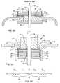
- FIG. 1is a cross-sectional view of the feedthrough terminal assembly disclosed is U.S. Pat. No. 5,333,095.
- the assembly 10includes a conductive ferrule 12 which is conductively connected to a housing or casing 14 of a human implantable device, such as a cardiac pacemaker, an implantable defibrillator, or a cochlear implant or the like.
- the assembly 10includes a feedthrough capacitor 16 having a grounding portion 24 which is conductively coupled to the ferrule 12 .
- At least one terminal pin or lead wire 18extends through the ferrule 12 , in non-conductive relation, and through the capacitor 16 in conductive relation.
- an alumina insulator 20is disposed between the terminal pin 18 and the ferrule 12 or other conductive substrate through which the terminal pin 18 passes through in non-conductive relation.
- the capacitor 16may be bonded to the insulator 20 or separated from the insulator 20 thereby forming an air gap depending on the assembly method used.
- the outside diameter metallization 24 of the capacitor 16is installed in conductive relation with the conductive substrate or ferrule 12 so that the ground electrodes of feedthrough capacitor 16 are properly grounded.
- An alternative arrangementis shown in U.S. Pat. No. 5,905,627, the contents of which are incorporated herein.
- FIG. 2illustrates the uni-polar monolithic ceramic feedthrough capacitor 16 of FIG. 1 , which is typical in the prior art described by the U.S. Pat. Nos. 5,333,095 and 4,424,551 patents and many others.
- Both inside diameter and outside diameters 22 and 24are metallized using a conductive termination which puts the respective electrode plate sets in parallel.
- the feedthrough capacitoris designed to have the lead wire 18 pass through the center of it.
- the lead wire or terminal pin 18is conductively coupled to the inner diameter metallization 22 so as to be conductively coupled to a first set of active electrodes 26 .
- a second set of ground electrodes 28are conductively coupled to the outer diameter metallization 24 for grounding to the conductive substrate or ferrule 12 .
- FIG. 3is the schematic diagram of the feedthrough capacitor of FIG. 2 .
- feedthrough capacitorsare three terminal devices which offer broadband performance and are best modeled by transmission line equations.
- Feedthrough capacitorsare novel in that they act like broadband transmission lines and have very low inductance properties. This means that they can provide effective EMI filtering immunity over very broad frequency ranges. They do this by de-coupling high frequency noise and shunting it to the overall titanium or stainless shield housing 14 of the implantable medical device. This is in contrast to rectangular monolithic chip capacitors and other two terminal capacitors which have a substantial amount of series inductance. Two terminal capacitors tend to self resonate at very low frequency and thus make very poor EMI filters, particularly for high frequencies such as cell phones, microwave ovens, radars and other emitters.
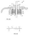
- FIGS. 4 and 5illustrate another type of capacitor 16 , which is a multi-hole micro-planar array quad-polar feedthrough capacitor. This has essentially the same properties as the previously described uni-polar feedthrough capacitor illustrated in FIGS. 2 and 3 , and can accommodate multiple terminal pins therethrough.
- FIG. 6is the schematic drawing of the quad-polar capacitor of FIGS. 4 and 5 .
- FIG. 7describes the capacitor reactance equation and illustrates how the capacitor reactance varies in ohms vs. frequency for an ideal capacitor.
- capacitorslook like open circuits (in other words, like they are not there).
- well-designed capacitorstend to look like a very low reactance in ohms (or short circuit). In this way, capacitors are frequency selective components and can be used to short out or bypass undesirable high frequencies thereby acting as low pass filter devices.
- implantable cardioverter defibrillatorswhich not only offer high voltage shock therapy to the heart, but also provide monitoring, anti-tachycardia pacing and conventional atrial and ventricular pacing.
- congestive heart failure devicesalso known on the market as biventricular pacemakers. All of these new devices have a need for an increased number of lead wires to be implanted within the heart or outside the vasculature of the heart. This has greatly complicated the loop coupling and antennae coupling areas for EMI induction. This also means that more lead wires must ingress and egress the implantable medical device. Accordingly, it is now common for 8-pin, 12-pin or even 16-pin devices to be present in the marketplace, all of which have unique filtering needs.
- Blue Toothis a method of interconnecting computers and the peripheral devices in a wireless manner. This also increases the number of digital signals to which an implantable device patient is exposed. Accordingly, there is an ever-increasing need for better EMI immunity of implantable medical devices over wider frequency ranges.
- Prior art EMI filters for medical implant applicationshave generally consisted of single pole devices consisting of a single feedthrough capacitor element on each lead wire. It is possible to increase the amount of attenuation of a single element feedthrough capacitor by raising the capacitance value. This also desirably lowers the frequency at which the capacitor starts to become effective. This is known as the feedthrough capacitor's 3 dB cutoff point. Unfortunately, raising the capacitance also has a number of undesirable side effects. First of all, too much capacitance can start loading down the output of an implantable medical device thereby degrading its operation. Too much capacitance can also be a problem in that excess energy dissipation can occur as the capacitor must be charged and discharged during cardiac pacing or digital signal processing in a hearing device.
- inductorperforms the opposite function in that the inductive reactance X L in ohms, as shown in FIG. 8 , varies directly with the frequency and the inductance in microhenries. This formula is applicable not only to multi-turn toroids, but single turn ferrite beads as well.
- the inductive reactance X Lis the opposite of capacitance reactance X c in that inductive reactance increases with increasing frequency. As illustrated, inductive reactance is zero ohms at DC and goes up to a very high value at high frequency.
- FIG. 9Common prior art EMI filter circuits are shown in FIG. 9 consisting of single element feedthrough capacitors “C”, “double element L 1 ” and “reverse L 2 ” filters, which combine an inductor and a capacitor, and other elements or other configurations including “PI” and “T” configurations.
- the commonly used prior art filter circuit for medical implant applicationshas been the “C” circuit or feedthrough capacitor. All of the cited patent references are based on a single element feedthrough capacitors bonded directly to or in close proximity to the hermetic terminal of an implantable medical device. However, using inductance in combination with a feedthrough capacitor increases the filter's effectiveness.
- the horizontal or X axisis frequency in MHz and the vertical or Y axis is the filtering efficiency measured as insertion loss in dB.
- the insertion lossincreases with frequency at a slope of 20 dB per decade.
- a two element filter like an “L” filtergoes up at a slope of 40 dB per decade. This means that its filtering effectiveness at high frequency is much greater than a single element filter. If one were to add inductors on both sides of the capacitor, it would become a three component filter, which would increase at 60 dB per decade and so on.
- a single element feedthrough capacitoris limited to an attenuation increase of 20 dB per decade. This is a linear function on semi log paper in the region that is well above the 3 dB cutoff point. In other words, for a single element feedthrough capacitor filter that offers 20 dB of attenuation at 10 MHz, that same filter would offer 40 dB at 100 MHz which is one frequency decade above. If one were to take the same feedthrough capacitor and combine with it an inductor element, thereby making it into an L section filter, this now becomes a 2-element filter. A 2-element filter will increase its attenuation effectivity by 40 dB per decade.
- a two element EMI filtercan be designed such that it offers very low attenuation in the cardiac sensing and telemetry ranges of the implantable medical device, but increases the attenuation curve very steeply above these frequencies. Accordingly, there is a need to provide multi-element filters for implantable medical devices.
- the feedthrough capacitorBy thereby raising and stabilizing the AIMD input impedance, the feedthrough capacitor, which is oriented toward the body fluid side, first intercepts and thereby becomes much more effective in bypassing high frequency EMI signals to the overall equipotential shield or housing of the AIMD. This shunting of undesirable signals prevents EMI signals from entering into the AIMD housing where they could interfere with proper AIMD circuit and therapy functions.
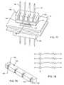
- FIGS. 11–15Exemplary ferrite beads and wire-wound inductors 30 – 34 are illustrated in FIGS. 11–15 .
- FIG. 15illustrates placing multiple turns of wire 36 through a ferrite or iron-core inductor element 34 . This is highly efficient because the inductance of the component goes up as the square of the number of turns. In other words, if one were to place a single turn or a straight lead wire 36 through the ferrite bead element or ferrite core 32 , this would be defined as one turn ( FIGS. 13 and 14 ). However, if one were to place additional turns, the inductance would go up as the square of the number of turns. FIG.
- the toroidal inductor materialcan be made of ferrite, powdered iron, molypermalloy or various other materials which affect inductive properties.
- ICDimplantable cardioverter defibrillators
- Typical values for filter feedthrough capacitors used in medical implant applicationsrange from 390 picofarads all the way up to 9000 picofarads.
- the average feedthrough capacitoris not very volumetrically efficient. Since only a few electrode plates are required to reach the desired capacitance value (due to the high dielectric constant), typical feedthrough capacitors used in medical implantable devices incorporate a number of blank cover sheets.
- a typical ceramic feedthrough capacitor used in an active implantable medical devicewould have a thickness between 0.040 and 0.050 inches. Of that, only about 1 ⁇ 3 to 1 ⁇ 2 of the total height is actually used to provide capacitance. The rest is used to provide mechanical strength.
- Implantable medical device hermetic terminalsalso pose another unique problem for providing substantial inductance in EMI filters. This comes from the nature of providing a hermetic seal to protect against intrusion of body fluids.
- a typical multi-turn inductor as described in many prior art applicationscan be held loosely in one's hands. One can grasp a length of wire 36 and pass it back and forth through the center forming a multi turn inductor 34 , as shown in FIG. 15 .
- the lead wireis solidly captured at one end by the nature of the hermetic terminal (usually by a gold braze or the like).
- the capacitormust be mounted to the hermetic terminal in accordance with one of the many prior art references.
- the EMI filteris designed to offer a very low attenuation in the cardiac sensing and telemetry ranges of the implantable medical device, but increase the attenuation curve very steeply above these frequencies to take into account the EMI produced by environmental emitters.
- Such filtersshould be volumetrically efficient so as to be the smallest possible size while having sufficient mechanical strength.
- Such filtersshould also be able to be hermetically sealed to protect against intrusion of body fluids into the implantable medical device.
- the present inventionfulfills these needs and provides other related advantages.
- the present inventionresides in a feedthrough terminal assembly which advantageously incorporates an inductor in the feedthrough capacitor assembly.
- Incorporating inductors in accordance with the present inventionrenders the EMI filter a two element (two-pole) or three element (three-pole) device and improves the EMI filter over wider frequency ranges. In particular, the filtering efficiency measured as insertion loss (dB) is greatly improved.
- Such assembliesare particularly suitable for human implantable device applications, such as cardiac pacemakers, implantable defibrillators, cochlear implants and the like.
- the inventioncomprises a feedthrough terminal assembly that includes a conductive ferrule, a feedthrough capacitor, and an inductor closely associated with the capacitor in non-conductive relation.
- the feedthrough capacitorincludes first and second sets of electrode plates. The second set of electrode plates are conductively coupled to the ferrule.
- a conductive terminal pinextends through the capacitor such that it is conductively coupled to the first set of electrode plates, and through the inductor in non-conductive relation.
- the feedthrough terminal assemblyis configured for use in an active implantable medical device.
- the conductive ferruleis conductively coupled to a housing for the active implantable medical device.
- such devicescomprise a cardiac pacemaker, an implantable defibrillator, a cochlear implant, a neurostimulator, a drug pump, a ventricular assist device, a gastric pacemaker, an implantable sensing system, or a prosthetic device.
- the inductoris bonded directly to the capacitor utilizing a non-conductive polyimide, glass, ceramic bonding material, epoxy, silicone, or a thermal plastic supportive tape adhesive.
- the inductortypically comprises a high permeability ferrite material.
- a high permeability ferrite materialmay be selected from scintered alloys of cobalt zinc ferrite, nickel zinc ferrite, manganese zinc ferrite, powdered iron, or molypermally.
- a conformal coatingis typically provided over the inductor.
- the coating disclosedcomprises Paralyne.
- an insulatoris typically disposed between the inductor and the terminal pin.
- the insulatormay comprise an epoxy, a thermal-setting non-conductive adhesive, a non-conductive polyimide, or a silicone material.
- a second inductoris provided through which the terminal pin extends in non-conductive relation.
- the first and second inductorsmay be disposed adjacent to one another or on opposite sides of the capacitor.
- at least one additional inductormay be stacked onto another one of the inductors, and such inductors may each be comprised of materials having different physical and electrical properties.
- the inductorsmay each be comprised of materials having the same physical properties.
- the capacitor and the inductormay be housed within the ferrule, and an insulative cap may be disposed over the inductor opposite the capacitor.
- the inductorsWhen the inductors are disposed on opposite sides of the capacitor, various configurations are possible. In one, at least one of the inductors may be disposed on a body fluid side of the feedthrough terminal assembly. Further, the second inductor may be disposed adjacent to the ferrule. Alternatively, the inductors may be bonded to opposing surfaces of the capacitor. In an illustrated embodiment wherein a pair of inductors are disposed on opposite sides of the capacitor, the capacitor and the inductors are disposed within and conductively isolated from the ferrule.
- first and second feedthrough capacitorsare associated with the inductor in non-conductive relation.
- the first and second feedthrough capacitorsmay be disposed on opposing surfaces of the inductor and, further, each capacitor may be internally grounded.
- the first and second capacitorseach include a first set of electrode plates conductively coupled to the terminal pin, and a second set of electrode plates conductively coupled to the ferrule.
- the first capacitorcomprises an internally and externally grounded capacitor
- the second capacitorcomprises an internally grounded capacitor.
- the feedthrough terminal assemblyfurther includes a conductive material extending through both the first and second feedthrough capacitors to conductively couple the second set of electrode plates to the second capacitor with the second set of electrode plates of the first capacitor.
- the conductive materialmay comprise a thermal setting conductive adhesive, a solder or a solder paste.
- the conductive materialmay comprise a conductive pin.
- the conductive pinmay comprise a nail head pin or a pin attached to an underlying hermetic insulator.
- the hermetic insulatoris typically disposed between the terminal pin and the ferrule, and the capacitor is typically disposed adjacent to the hermetic insulator.
- the inductorincludes an aperture aligned with an aperture of the capacitor through which a leak detection gas can be detected.
- the capacitor's second set of electrode platesmay be externally grounded to the ferrule, or, alternatively, internally grounded to a ground pin which is conductively coupled to the ferrule.
- the terminal pinmay be wound about the inductor to form multiple turns.
- adjacent portions of the wound terminal pinare electrically insulated from one another.
- the adjacent portions of the wound terminal pinare encased in a non-conductive material such as a non-conductive sleeve.
- the inductormay include a notch for receiving the wound terminal pin.
- the notchmay include a ramp for accommodating the terminal pin, and further the inductor may include multiple notches, each for accommodating a separate terminal pin therein.
- the notchincludes multiple slots for receiving corresponding multiple turns of the terminal pin.
- the notchmay further comprise contoured corners for accommodating the terminal pin.
- meansare illustrated for maintaining the conductor in close association with a capacitor without forming a direct physical attachment therebetween.
- the inductor maintaining meanscomprises a lock between the terminal pin and the inductor.
- the locktypically comprises a mechanical lock such as a swage, a clamp or an epoxy.
- the lockmay, alternatively, simply comprise a deformation in the terminal pin.
- the inductor maintaining meansmay further comprise a wire bond pad attached to the terminal pin.
- a wire bond padmay or may not be physically attached to the underlying structure of the hermetic terminal assembly apart from the terminal pin itself.
- FIG. 1is a cross-sectional view of a surface prior art mounted discoidal capacitor in an EMI filter assembly
- FIG. 2is a partially sectioned prior art uni-polar discoidal feedthrough capacitor of FIG. 1 ;
- FIG. 3is a schematic drawing of the feedthrough capacitor of FIG. 2 ;
- FIG. 4is a perspective view of a prior art quad-polar feedthrough capacitor
- FIG. 5is a cross-sectional view taken on the line 5 — 5 in FIG. 4 ;
- FIG. 6is a schematic drawing of the quad-polar capacitor of FIG. 4 ;
- FIG. 7describes the capacitor reactance equation and illustrates how the capacitor reactance varies in ohms vs. frequency for an ideal capacitor
- FIG. 8illustrates the equation for the inductive reactance
- FIG. 9illustrates schematic diagrams of common EMI filter circuits
- FIG. 10is a comparison chart of insertion loss vs. number of components in a low pass EMI filter
- FIG. 11is a perspective view of a prior art ferrite slab toroidal inductor
- FIG. 12is a cross-sectional view taken generally along line 12 — 12 , of FIG. 11 ;
- FIG. 13is a perspective view of a prior art toroidal ferrite inductor with one turn or a single pin going through the center thereof;
- FIG. 14is a cross sectional view of the toroid of FIG. 13 taken generally along line 14 — 14 ;
- FIG. 15is a perspective view of a prior art toroidal inductor with multiple lead wire turns
- FIG. 16is a chart giving the mechanical properties of a thermal plastic polyimide supportive tape adhesive which can be used in accordance with the present invention.
- FIG. 17is a cross-sectional view of an EMI filter embodying the present invention.
- FIG. 18is an enlarged view of the area 18 taken from FIG. 17 , illustrating an alternative embodiment
- FIG. 19is a schematic drawing of the EMI filter of FIG. 17 ;
- FIG. 20is a perspective view of the ferrite slab inductor 46 of FIG. 17 ;
- FIG. 21is a cross-sectional view of an EMI filter assembly embodying the present invention, illustrating multiple inductors 46 and 46 ′ in stacked or laminated relationship;
- FIG. 22is a schematic drawing of the EMI filter assembly of FIG. 21 ;
- FIG. 23is an exploded perspective view of the laminated inductors of FIG. 21 ;
- FIG. 24is a cross-sectional view illustrating placement of the ceramic capacitor and inductor completely inside of a surrounding ferrule
- FIG. 25is an electrical schematic drawing of the two-element inductor capacitor EMI filter of FIG. 24 ;
- FIG. 26illustrates an exploded perspective view of a five pole or penta polar capacitor assembly that is internally grounded embodying the present invention
- FIG. 27is a cross-sectional view of an EMI filtered hermetic terminal assembly modified by shortening the alumina insulator thereof to provide a convenient bonding surface to install a second ferrite bead 46 ′ on the body fluid side of the assembly;
- FIG. 28illustrates the second ferrite slab of FIG. 27 ;
- FIG. 29is a schematic drawing of the filtered hermetic terminal assembly of FIG. 27 ;
- FIG. 30is a cross-sectional view of an EMI filtered assembly having a ceramic capacitor disposed on the body fluid side and an inductor bonded to an internal insulator;
- FIG. 31is a cross-sectional view of an EMI filtered assembly embodying the present invention having inductors co-bonded to opposing surfaces of a ceramic capacitor;
- FIG. 32is an electrical schematic drawing of the EMI filter terminal assembly of FIG. 31 ;
- FIG. 33is a cross-sectional view of a PI filter assembly embodying the present invention.
- FIG. 34is an electrical schematic drawing of the EMI filter of FIG. 33 ;
- FIG. 35is a cross-sectional view illustrating a novel PI section filter incorporating capacitors combining both external and internal ground technologies
- FIG. 36is an electrical schematic view of the terminal of FIG. 35 ;
- FIG. 37is one possible top plan view of the assembly of FIG. 35 ;
- FIG. 38is a top plan view of another possible configuration of the assembly of FIG. 35 ;
- FIG. 39is a cross-sectional view illustrating another PI filter assembly incorporating hybrid capacitors similar to FIG. 35 ;
- FIG. 40is a cross-sectional view illustrating yet another novel PI filter assembly incorporating hybrid capacitors
- FIG. 41is a perspective view of the bottom capacitor of FIGS. 35 , 39 and 40 ;
- FIG. 42is a cross-sectional view through the capacitor of FIG. 41 taken generally along line 42 — 42 ;
- FIG. 43is a cross-sectional view through the capacitor of FIG. 42 taken generally along line 43 — 43 , illustrating the arrangement of active electrode plates;
- FIG. 44is a cross-sectional view through the capacitor of FIG. 42 taken generally along line 44 — 44 , showing the configuration of the ground electrode plates;
- FIG. 45is a perspective view of the ferrite inductor of FIG. 35 ;
- FIG. 46is a cross-sectional view of the inductor of FIG. 45 taken generally along line 46 — 46 ;
- FIG. 47is a perspective view of the upper capacitor of FIGS. 35 , 39 and 40 ;
- FIG. 48is a cross-sectional view of the capacitor shown in FIG. 47 taken generally along line 48 — 48 ;
- FIG. 49is a sectional view of the capacitor of FIG. 48 taken generally along line 49 — 49 , illustrating the arrangement of the active electrode plates;
- FIG. 50is a cross-sectional view of the capacitor of FIG. 48 taken generally along line 50 — 50 , showing the configuration of the ground electrode plates;
- FIG. 51is a perspective view of an internally grounded three-element PI circuit hermetic terminal embodying the present invention.
- FIG. 52is a sectional view taken generally along line 52 — 52 of FIG. 51 ;
- FIG. 53is a family of performance curves illustrating the advantages of adding the inductor filter elements of the present invention.
- FIG. 54is a perspective view illustrating an alternative embodiment of a ceramic capacitor and inductor mounted to a hermetic terminal and having a center hole therethrough, which allows for ready passage of a gas during hermetic seal testing;
- FIG. 55is a cross-sectional view of the assembly of FIG. 54 taken generally along line 55 — 55 , showing the inductor bonded to the capacitor with the aligned center hole for helium leak detection;
- FIG. 56illustrates an internally grounded tri-polar capacitor
- FIG. 57is a cross-sectional view taken generally along line 57 — 57 of FIG. 56 ;
- FIG. 58is a plan view of an inline multi-polar EMI filter with a grounded pin
- FIG. 59is a cross-sectional view taken generally along line 59 — 59 of FIG. 58 ;
- FIG. 60is a schematic diagram of the EMI filter assembly of FIGS. 58 and 59 ;
- FIG. 61is a top plan view of a multi-polar EMI filter with a grounded pin, similar to FIG. 58 ;
- FIG. 62is a cross-sectional view taken generally along line 62 — 62 of FIG. 61 , illustrating the use of an inductor slab instead of individual inductor beads;
- FIG. 63is a perspective view of a novel inductor having a notch in accordance with a preferred embodiment of the present invention.
- FIG. 64is a cross-sectional view taken generally along the line 64 — 64 of FIG. 63 ;
- FIG. 65is a view similar to FIG. 64 , incorporating a ramp for facilitating feed of a multiple turn lead wire through the center hole of the ferrite inductor;
- FIG. 66is an electrical schematic drawing of the ferrite bead of FIG. 63 ;
- FIG. 67is a sectional view similar to FIG. 17 , but employing the novel ferrite bead of FIG. 63 ;
- FIG. 68illustrates the schematic diagram of the EMI filtered terminal assembly of FIG. 67 ;
- FIG. 69is an enlarged fragmented perspective view of a portion of the terminal lead shown in FIG. 67 , illustrating that a portion of an insulator is removed from the lead as it extends upwardly through the capacitor;
- FIG. 70is a perspective view of a uni-polar ferrite slab designed with a novel slot arrangement
- FIG. 71is a cross-sectional view taken generally along the line 71 — 71 of FIG. 70 ;
- FIG. 72is a cross-sectional view illustrating a uni-polar feedthrough capacitor utilizing the ferrite slab of FIG. 70 ;
- FIG. 73is a fragmented perspective view of a novel two-turn uni-polar inductor embodying the present invention.
- FIG. 74is a perspective view of a uni-polar ferrite slab with four slots
- FIG. 75is a perspective view illustrating the novel four-turn uni-polar ferrite of FIG. 74 mounted to a hermetic terminal and assembled;
- FIG. 76is a perspective view of an inline quad-polar ferrite bead having four slots in accordance with the present invention.
- FIG. 77is a perspective view illustrating the mounting of the inline quad-polar ferrite bead of FIG. 76 to a hermetic terminal;
- FIG. 78is the schematic drawing of the quad-polar “L” section filter shown in FIG. 77 ;
- FIG. 79is a perspective view of a ferrite slab embodying the present invention and having novel slots so that an additional turn can be added making the unit into a two-turn inductor;
- FIG. 80is a perspective view of a quad-polar feedthrough filter terminal assembly wherein the inductor slab is loosely seated on top of the capacitor without any bonding material;
- FIG. 81is a sectional view taken generally along the line 81 — 81 of FIG. 80 ;
- FIG. 82is a perspective view of a quad-polar feedthrough filter terminal assembly similar to that illustrated in FIGS. 80 and 81 , illustrating another embodiment thereof;
- FIG. 83is a sectional view taken generally along the line 83 — 83 of FIG. 82 ;
- FIG. 84is a sectional view similar to that illustrated in FIG. 17 , illustrating an L-shaped wire bond pad attached using bonding insulating material to the inductor slab;
- FIG. 85is a perspective view of the L-shaped wire bond pad of FIG. 84 ;
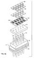
- FIG. 86is an exploded perspective view of an octapolar (plus a grounded lead) feedthrough filter terminal assembly embodying the present invention.
- FIG. 87is a perspective view of the feedthrough terminal assembly of FIG. 86 ;
- FIG. 88is an enlarged cross-sectional view taken generally along the line 88 — 88 of FIG. 87 .
- the present inventionresides in an EMI filter feedthrough terminal assembly which incorporates an inductive element in order to increase attenuation of EMI as the frequency of the EMI increases.
- the inventionis particularly suited for use in human implantable medical devices, as described above.
- an EMI filter feedthrough terminal assembly 36 embodying the present inventionis illustrated. Similar to typical implantable device application assemblies, the assembly 36 includes a conductive substrate in the form of a ferrule 12 which is conductively coupled to the housing or casing 14 of an implantable medical device using a laser weld, braze 38 or other appropriate conductive connection as is well-known in the art.
- a feedthrough capacitor 40is conductively coupled to the ferrule 12 using a conductive thermal setting material, braze, solder, etc. 42 ′.
- a lead wire or terminal pin 18extends through apertures formed in the ferrule 12 and capacitor 40 .
- Active electrodes 26 of the capacitor 40are conductively coupled to the terminal pin 18 , by solder, conductive thermal setting material, braze 42 or other means that are well-known in the art.
- Ground electrodes 28 of the capacitor 40are conductively coupled to the ferrule 12 , in this instance between outer metallization 24 of the capacitor 40 and its conductive connection 42 ′ to the ferrule 12 .
- An insulator 20such as an alumina ceramic, is disposed between the conductive ferrule 12 and the terminal pin 18 so that the terminal pin 18 is in non-conductive relation thereto.
- the terminal pin 18may be adhered or otherwise fixed to the insulator 20 by means of gold braze 44 or a glass compression or fusion seal or the like.
- the present inventionadvantageously incorporates an inductor 46 into the assembly 36 .
- the ferrite slab inductor 46is co-bonded to the capacitor 40 so as to be in non-conductive relationship therewith.
- the capacitor element 40is schematically oriented towards the body fluid side and the inductor element 46 is desirably oriented toward the inside of the implantable medical device 14 .
- the reason it is desirable to have the feedthrough capacitor C oriented towards the body fluid side from an electrical circuit point of viewis that the cardiac lead wire system represents a fairly stable source impedance. Studies indicate that the source impedance of implanted lead wires tend to be around 80 ohms. This does vary somewhat with frequency, but this is a reliable average.
- the input impedance of a cardiac pacemaker or other implantable medical deviceis highly variable with frequency.
- the input impedance of a cardiac pacemakertends to be relatively high, on the order of 10 Kohms or more.
- the input impedance of the cardiac pacemakercan vary dramatically.
- the AIMD input impedance (Z IN )can shift due to parasitic resonances and coupling between stray capacitance and stray inductance of circuit traces and other components. Accordingly, at certain frequencies the input impedance of the pacemaker might be hundreds of ohms and at a nearby or adjacent frequency the input impedance could plummet drastically to less than 2 ohms.
- a feature of the inductor L as described in the present inventionis that the inductive element stabilizes the input impedance of the cardiac pacemaker.
- the feedthrough capacitor Cbecomes much more effective as a bypass element.
- EMIwhen EMI is induced on the cardiac lead wires, that EMI comes from a source impedance of approximately 80 ohms. It then encounters the feedthrough capacitor C which represents a very low impedance to ground.
- the inductive element Lalso blocks the EMI from getting into the input circuits of the implantable medical device because, by representing a relatively high impedance, the EMI is desirably shunted to ground through the feedthrough capacitor C.
- the terminal pin 18extends through an aperture 48 of the inductor 46 .
- the space between the lead wire 18 and the inside diameter of the inductor 46defines an air gap 49 .
- This air gapis desirable in that there is no electrical connection at all required between the inductor 46 and the lead wire 18 .
- the air gap 49does not present a problem.
- air gap 49needs to be controlled.
- the aperture 48is aligned with apertures in the capacitor 40 and ferrule 12 .
- the assembly 36becomes a two element “L” circuit EMI filter. As shown in FIG. 10 , this has the desired effect of greatly increasing the insertion loss or filtering efficiencies throughout the frequency range. Whereas a single component “C” filter, such as that illustrated in FIG. 1 , has an insertion loss slope of 20 dB per decade, the two component “L” filter circuit of FIG. 17 has a 40 dB per decade slope, which is highly desirable.
- the volumetric efficiency of the capacitor 40 in the inventionis enhanced as the co-bonding of the inductor element 46 creates a monolithic structure which has sufficient height for mechanical strength of handling and construction.
- FIG. 1one can observe the height of the typical capacitor 16 illustrated.
- FIG. 17one can see the composite structure consisting of the thinner capacitor 40 and the co-bonded ferrite slab 46 , which composite structure has approximately the same height as the original capacitor 16 shown in FIG. 1 . This is because the internal electrode plates of the capacitor 16 of FIG. 1 are very efficient and do not require the entire height of the ceramic capacitor 16 .
- Cover sheets or layersare typically added on the top and bottom of the capacitor 16 as shown in FIG. 1 , to increase its structural integrity. Another way of saying this is that it is really not possible to build ceramic feedthrough capacitors that are too thin. That is, if they are designed below 0.030 inch in thickness, warpage and cracking during sintering become major factors (this is known in the industry as the potato chip effect). Accordingly, cover sheets are built up to strengthen the ceramic capacitor. In the structure shown in FIG. 17 , the co-bonding of the ferrite inductor provides the required strength. Accordingly, the capacitor 40 can be made much thinner.
- the insertion of the lead wire or terminal pin 18 directly through the inductive element 46creates a single turn inductor. As shown in FIG. 10 , this single turn increases the attenuation rate of the assembly 36 from 20 dB/decade to 40 dB/decade.
- the inductor 46 capacitor 40 combinationis desirably on the inside of the ferrule 12 . That is on the inside of the pacemaker or implantable medical device housing 14 that is protected from body fluids by the hermetic seal 20 .
- the electronic components of an active implantable medical deviceare preferably placed inside the hermetic terminal to protect them from the corrosive and conductive effects of body fluid intrusion.
- FIG. 17one can see that there is an air gap 49 between the lead wire 18 and the inside diameter of the ferrite slab 46 .
- Thisis not a problem in a low voltage application such as for an implantable cardiac pacemaker.
- this air gap 49can present a problem. That is because micro-coulomb or arc type discharges can occur in the high voltage field generated around the lead wire 18 and the inside diameter of the ferrite slab 46 . This can occur even though the ferrite slab 46 has been conformally coated with a material such as Paralyne or equivalent insulating materials.
- the high voltage field that surrounds lead wire 18tends to relax into the air space surrounding it.
- FIG. 18illustrates this same air gap 49 which has been back filled with an insulating material 51 .
- This insulating materialcan be a polymer including an epoxy, a thermal-setting non-conductive adhesive, a non-conductive polyimide, a silicone, a glass, a ceramic or or air holes.
- the presence of the filling material 51puts a high dielectric strength material into the previously mentioned air gap 49 . This prevents the formation of micro coulomb discharges or arcing.
- the inductor 46is typically in the form of a ferrite slab, as illustrated in FIG. 20 .
- Ferrite beads and slabsare typically formed during a powder pressing and sintering manufacturing process (extrusion or machining techniques can also be used).
- Proprietary powdersincluding powdered iron, manganese zinc ferrite, nickel zinc ferrite, cobalt zinc ferrite, etc. are formed into the beads or slabs of the final toroidal inductor configuration.
- the inductor 46may be comprised of other materials such as a molypermalloy material or other high permeability ferrite material. There are commercially available ferrite materials that have both high permeability and high resistivity properties, making them ideal for medical implant EMI filter applications.
- Ferritesare hard ceramic materials which can abrade wire insulation films during winding.
- the inductor slab 46is ordinarily tumbled so that sharp edges are rounded.
- a smooth insulative conformal coatingcan be provided. This coating should be soft to prevent stressing and cracking the core upon curing or during any temperature cycling or temperatures due to bonding.
- the coatingshould have a low coefficient of friction and withstand normal environments. Therefore, in an embodiment of the invention, such ferrite bead or ferrite slab 46 is coated with suitable insulation materials such as Paralyne C, Paralyne D, Paralyne E or Paralyne N or other suitable conformal coating material.
- a conformal coating materialalso desirably increases the electrical insulation resistance of the inductor 46 to a very high value (within the Megohm or Gigohm range). Accordingly, the conformal coating will also serve to prevent premature battery drain of the implantable medical device.
- FIG. 16illustrates the properties of a thermal plastic polyimide supportive tape adhesive 50 or 50 ′ which can be used as shown in FIG. 17 to co-bond the inductor 46 to the capacitor 40 .
- This tape adhesive 50 or 50 ′is ideal for bonding the capacitor 40 to the ferrite slab inductor 46 .
- This materialhas unique properties and it can be di-cut or laser-cut to any desired shape with a variety of through holes. It adheres well to the ceramic capacitor 40 , alumina 20 , inductor conformal coating, and other surrounding materials, thereby providing a convenient bonding methodology.
- the inductor slab 46has both an inductive property L and series resistance property R L . It is a property of ferrite materials that both the inductance and the resistive properties vary with frequency. In general the inductance tends to be higher at low frequency and goes down with elevating frequency. On the other hand R L tends to be a very low number at lower frequencies and tends to get higher in its ohmic value at higher frequencies. This is particularly desirable in an implantable medical device where biologic signals at very low frequencies are being detected by pacemaker sense circuitry. It is a feature of the present invention that R L be quite low at biologic frequencies so that sensing such frequencies is not impaired.
- R Lacts dramatically to increase the EMI filter performance of the L section filter as shown on the schematic diagram in FIG. 19 .
- the way an L section filter worksis that EMI is shunted to ground through the feedthrough capacitor 40 .
- the inductive reactance X L and the resistance of the ferrite slab R Lboth act to raise the input impedance of the implantable medical device. This makes the operation of the feedthrough capacitor assembly 36 much more effective. In other words, the attenuation of the EMI filter capacitor assembly 36 is dramatically improved as both L and R L go up. Therefore, it is a feature of the present invention that inductor slab 46 have two desirable properties including the property of inductance and high frequency resistance R L .
- the inside diameter hole 48 of the ferrite slab 46fit relatively tightly to the feedthrough lead wire 18 .
- the inductance L and the resistive property R Lcan be as high as practicable. This can be done by increasing the overall height of the ferrite bead 46 .
- practical manufacturing restrictionsexist. These restrictions are based on the fact that, in general, the ferrite slab material 46 is created by a pressed and sintered powder system. The powder is pressed into a die with a central pin which is later extracted after sintering at high temperature. If the ferrite slab 46 gets too thick, it becomes virtually impossible to extract the fixture pin after sintering of the ferrite material into a hard structure.
- the inductor slab 46Another factor that limits the height of the ferrite slab 46 is the amount of physical space that is available inside of the implantable medical device. It is extremely important that every component in an implantable medical device be kept very small, so that the size and weight of the overall medical device is comfortable for the patient and also convenient for surgical implant. However, in some devices there is considerable height that is available. Accordingly, it is preferred that the inductor slab 46 have as much height as possible for a given design.
- FIGS. 21 and 23illustrate a novel feature of the present invention in that ferrite slabs with a very small center hole can be manufactured and then layered to provide the overall height to optimize both the inductive and resistive properties.
- FIG. 21one sees that there are two ferrite slabs 46 and 46 ′ which have been bonded together with a non-conductive insulating washer 50 ′′ (see FIG. 16 ). This allows one to increase the overall height of the ferrite slab without running into the fixturing problems if one tried to manufacture this as a single element. As previously mentioned, for a single inductor slab, the height and inside diameter ratio could be quite problematic in the manufacturing operation.
- FIG. 22illustrates the effect of having these two inductors 46 and 46 ′ acting in series with their two resistive properties acting in series. These elements simply add up which increases the overall inductance and the overall resistance of the ferrite slab. However, this does not change the basic L circuit EMI filter configuration. In other words, the addition of a second ferrite slab 46 ′ means that the EMI filter of FIG. 21 still acts as a two element L section filter. It is only when you separate the ferrite slabs by a capacitor element that you increase the number of poles or elements of the EMI filter, as described further herein.
- a plurality of ferrite slabs 46 and 46 ′can be co-bonded together.
- These slabscan be of various initial permeabilities and properties.
- the first slab 46could be of manganese zinc material and slab 46 ′ could be of cobalt zinc material.
- These two materialshave markedly different electrical properties.
- One materialhas higher inductance at low frequency whereas the other material has higher inductance at higher frequencies.
- By co-bonding beads or slabs 46 and 46 ′ of various materials togetherone can optimize inductance throughout wider frequency ranges.
- the resistive property R L1 and R L2 Of the two ferrite slabs 46 and 46 ′Each type of ferrite material has different resistance versus frequency properties. By combining various materials one can also optimize the amount of resistance versus frequency.
- FIG. 24Another novel method of building an L circuit filter is the embedded approach, illustrated in FIG. 24 .
- the ceramic capacitor 40has been placed completely inside a surrounding ferrule 12 .
- the inductor slab 46is then co-bonded to the capacitor 40 , preferably oriented toward AIMD circuitry as illustrated.
- This electrical connection from the capacitor outside diameter metallization 24 and gold braze 44 ′ of ferrule 12is performed using connection material 42 ′ in accordance with U.S. patent application Ser. No. 10/377,086, the contents of which are incorporated herein, utilizing oxide resistant biostable conductive pads.
- An optional epoxy cap 52can be placed over the top of the ferrite inductor 46 , primarily for cosmetic purposes.
- the resulting L circuitis illustrated in the schematic diagram of FIG. 25 , which as shown in FIG. 10 gives rise to an attenuation slope of 40 dB/decade.
- FIG. 26illustrates an exploded view of an internally grounded pentapolar feedthrough capacitor hermetic terminal 54 with mounted feedthrough capacitor 40 , inductor 46 , and alumina insulator 20 with five gold brazed leadwires 18 which are typically platinum, or platinum-iridium or the like.
- a ground plate 56is typically attached to the ferrule 12 by laser welding or the like.
- An insulating washer 50is then placed on top of the ground plate 56 .
- An internally grounded feedthrough capacitor 40 in accordance with U.S. Pat. No. 5,905,627is then placed and attached to the lead wires 18 .
- Insulating washer 50 ′is then placed on top of capacitor 40 to which inductor 46 is assembled in accordance with the present invention. Accordingly this makes a very efficient pentapolar L section filter.
- FIG. 27illustrates a three element “T” section low pass filter assembly 58 wherein there are ferrite slab inductor elements 46 and 46 ′ which appear electrically on both sides of the feedthrough capacitor 40 .
- Such a three-element filterwill have an attenuation rate of 60 dB per decade, as shown in FIG. 10 , which is even more highly desirable.
- Thisis also shown as the T circuit schematic of FIG. 29 .
- Another feature of the invention as shown in FIG. 27is that there is a biocompatible conformal coating over the ferrite bead inductor element 46 ′. This provides an additional level of protection from intrusion of body fluid in the inductor element 46 ′.
- the inductor element 46 ′is encapsulated underneath the pacemaker or implantable defibrillator header block (not shown). This provides additional protection from the intrusion of body fluid.
- the inductor 46 ′placed on the body fluid side is accomplished in three main ways. That is, the ferrite material is a hard fired material that in and of itself is not prone to leaching out and therefore has its own degree of biocompatibility.
- the adjunct conformal coating of silicone, Paralyne or other biocompatible coatingassists in its biocompatibility as well as the placement of adjunct sealants in the header block.
- a ferrite slab inductor 46is co-bonded directly to the ceramic capacitor 40 , such as by an adhesive washer 50 ′.
- a second inductor slab 46 ′is bonded directly to the hermetic terminal 12 , such as by an adhesive washer 50 ′′′.
- the inductor ferrite bead or the inductor slab 46 ′is directly exposed to body fluid or on the body fluid side of the device 14 .
- a header or connector assembly(not shown) is placed over this area with some sort of a sealant such as silicone and the like.
- a unique aspect of the inventionis the use of ferrite material which during sintering is highly bound to various elements including iron. This makes the composite structure biocompatible. Examples of such ferrite material include Manganese Zinc, Nickel Zinc or Cobalt Nickel.
- FIG. 30illustrates a novel L section filter 60 of the present invention with the inductor slab 46 bonded to the inside of the hermetic terminal 12 , such as by a washer 50 ′′′.
- the ceramic feedthrough capacitor 40is shown on the outside or body fluid side of the device. In this case there is no conformal coating over the top of the capacitor 40 .
- the materials of the ceramic feedthrough capacitor 40must all be biocompatible. That is the internal electrodes 26 and 28 , the metallization 22 and 24 and the connections 42 ′ from the ferrule 12 to the outside diameter metallization 24 and from the lead 18 to the inside diameter metallization 22 must be of suitable biocompatible materials, as described in U.S. patent application Ser. No. 10/778,954, filed Feb. 12, 2004.
- Another advantage of designing with an L or T circuithas to do with the timing of the output circuitry of implantable cardioverter defibrillators. It has been noted that the presence of an EMI ceramic feedthrough capacitor in the high voltage output circuits of an implantable defibrillator can interfere with its timing or cause microprocessor re-sets. This is particularly true when the implantable defibrillator is fired into a no load situation. In other words, this is when the ICD lead wires would not be connected to cardiac tissue.
- the leading edge from the implantable defibrillator's pulsecauses excessive charging current into the feedthrough capacitor.
- the energy storedcan then reflect back and disrupt implantable defibrillator timing circuitry.
- the presence of the slab inductor 46 as described throughout this patent applicationis an advantage in that the series inductance will slow the rise time of this leading edge pulse before it gets to the feedthrough capacitor.
- higher capacitance value feedthrough capacitorscan be used in combination with an inductor without disrupting the sensitive output circuitry of the implantable defibrillator. This is because the series inductance decouples the feedthrough capacitor from the ICD's output circuitry.
- a novel T filter assembly 62includes two inductor ferrite slabs 46 and 46 ′, which are co-bonded to opposing top and bottom surfaces of the ceramic capacitor 40 within the ferrule 12 such as by insulating washers 50 and 50 ′′′.
- the schematic of the FIG. 31 “T” filteris shown in FIG. 32 .
- This filter assembly 62has an attenuation slope of 60 dB per decade, similar to the filter illustrated in FIG. 27 .
- insulating washer 50 ′′′is first placed into the cavity formed by the ferrule 12 .
- the inductor 46is then placed on top of the adhesive layer of 50 ′′′ and cured in place.
- an insulative layer 50 ′ and a capacitor 40are placed and cured thereby forming a laminate structure.
- the electrical connections 42 ′ between the capacitor outside diameter metallization 24 and the ferrule 12 and the capacitor lead wire 18 and the inside diameter metallization of the capacitor 22are then formed, such as by the insertion of a conductive thermosetting polymer, a solder, liquid solder, solder paste, brazing or the like ( 42 ).
- the thermal setting conductive material 42 or 42can be injected using a syringe into the annular space between the ferrule and the feed through capacitor-inductor stack and between the annular space surrounding lead wire 18 in the inside diameter of the capacitor and corresponding conductor stack.
- a preferred methodology of injecting the conductive material 42 and 42 ′is through centrifuge methods. This is best accomplished by inverting the assembly shown in FIG. 31 and injecting a thermal setting conductive adhesive in its liquid state flooding the entire surface of inductor 46 . This material would fill the entire cavity that is formed above inductor 46 and within the inside diameter of ferrule 12 .
- the entire assemblyis then centrifuged which injects the thermal setting conductive material 42 and 42 ′ down into the annular spaces as previously described. Typically, a cleaning operation would be followed after this step. At this point an insulating washer 50 ′ with adhesive backing is placed and an inductor 46 ′ is placed on top of the capacitor 40 and seated. There is a final curing operation which co-bonds the entire structure which results in a laminate beam consisting of the inductor 46 , the capacitor 40 and the inductor 46 ′.
- insulative washers 50 ′ and 50 ′′′are designed to be the same as dimensionally and to conform to the outside diameter of the capacitor 40 and the outside diameter of the ferrite slabs 46 and 46 ′. This is important because it allows the conductive thermal setting polyimide or solder 42 and 42 ′ to directly contact the gold braze 44 and 44 ′. Directly contacting the gold braze as opposed to contacting the titanium is very important to avoid the formation of titanium oxides which can preclude the proper operation of the EMI filter capacitor. This is fully described in pending U.S. patent application Ser. No. 10/377,086.
- the lead wire 18can then be of any biocompatible material including the group of niobium, tantalum and the like.
- ferrite slab 46has been conformably coated with a suitable insulating material. This is done prior to assembling ferrite slabs 46 and 46 ′ into the assembly shown in FIG. 31 .
- suitable conformal coating materialsexist in the art and would consist of the group of thermal setting polymers and the like. Two preferred materials are Paralyne C or Paralyne D. These materials are vapor deposited and have excellent dielectric breakdown strength measured in volts per mil. Paralyne D has a higher temperature rating and is ideally suited for use in a hermetic terminal of an implantable medical device.
- connection materials 42 and 42 ′are also desirably of high temperature ratings. For example, a high temperature solder such as SN10 can be used or a thermal setting conductive polyimide which can easily withstand temperature above 300 degrees centigrade.
- conformal coatings on the ferrite slabs 46 or 46 ′is for applications in a high voltage device such as an implantable cardioverter defibrillator.
- a high voltage devicesuch as an implantable cardioverter defibrillator.
- Paralyne coatingsare preferred because they have voltage breakdowns in excess of 1000 volts per mil.
- a conformal coating of 2–3 milsallows the ferrite slab to withstand voltages of greater than 2000 volts.
- a novel PI filter 64is shown in FIGS. 33 and 34 .
- a PI circuit filteris a three-element filter which offers a three element attenuation slope of 60 dB per decade (see FIG. 10 ). This is the same as the slope for the T element filter that was previously described.
- a ferrite slab inductor 46has been sandwiched between two feedthrough capacitors 40 and 40 ′ as shown. Insulative washers 50 ′ bond and prevent conductive contact between the inductor 46 and capacitors 40 and 40 ′. Conformal coating on all surfaces of inductor 46 prevents electrical contact between the pin 18 , the pin electrical connection material 42 , and the inductor 46 . Space has been allowed so that the conductive thermal setting materials, such as a silver filled conductive polyimide, can directly contact the gold braze in accordance with pending U.S. patent application Ser. No. 10/377,086.
- FIG. 35illustrates a novel PI section filter 68 which incorporates surface mounting techniques.
- the bottom capacitor 70is a special hybrid capacitor in that it combines both external ground and internal ground technologies. Externally grounded feedthrough capacitors are well known in the art. Internal grounding is described by U.S. Pat. No. 5,905,627.
- the schematic for this PI circuit deviceis shown in FIG. 36 . As shown, it is a three element low pass EMI filter which, as shown in FIG. 10 , offers 60 dB per decade of attenuation.
- the special hybrid capacitor 70is seated to the hermetic terminal 12 by way of an insulating washer 50 .
- the hybrid capacitor 70is externally grounded to the gold braze 44 ′ of the ferrule by conductive material 72 .
- the capacitor 70 active electrode plates 26are also connected to leadwires 18 by conductive material 74 .
- An inductor slab 76is then bonded to the top of capacitor 70 by way of an insulating washer 50 ′.
- a top capacitor 78is then placed on top of another insulating washer 50 ′ and cured in place to form the laminated stack assembly 68 as shown.
- Capacitor 78is a conventional internally grounded feedthrough capacitor, as described by U.S. Pat. No. 5,905,627, the contents of which are incorporated herein.
- the arrangement of FIG. 35allows for the upper capacitor 78 to be grounded to the lower capacitor 70 by conductive material 80 so that it forms an effective PI circuit filter or three element filter capable of 60 dB per decade.
- the conductive material 80can be a variety of materials from the group of the thermosetting conductive adhesives such as a conductive epoxy or conductive polyimide, solder or solder paste, and a variety of other conductive materials. It should also be noted that there is an optional insulating surface 82 which prevents the conductive material 80 from shorting to the ferrite bead 76 . This can be a conformal coat such as Paralyne C or Paralyne D which surrounds all surfaces of inductor 76 or can be an inserted insulating sleeve 82 .
- FIGS. 37 and 38show two different top views of FIG. 35 illustrating that this technology can be manufactured in either round (discoidal), rectangular, or other geometries.
- the number of lead wires 18can be varied in accordance with the intended application.
- FIG. 39is a variation of FIG. 35 in that the fill material 80 has been replaced by a conductive pin 84 .
- this pin 84would have a nail head configuration as illustrated, which would increase its pull strength as it is captured by the surrounding solder or conductive thermosetting polymeric materials.
- the pin 84could be comprised of a variety of materials including extruded copper, steel, titanium or the like.
- the pinwould be electroplated with tin, silver or a similar solder wettable coating. Since this is on the inside (non-body fluid side) of the device, there is no need for any of the connection materials or the pin to be biocompatible.
- FIG. 40is yet another modification of the principals of the PI circuit filter shown and previously described as FIG. 35 .
- the center pin 86connects the ground electrode plates 28 of the hybrid capacitor 70 with the ground electrode plates 28 ′ of internally grounded capacitor 78 .
- This pin 86has the greatest pull strength of all the configurations in that the pin 86 is seated into the aluminum ceramic insulator 20 and mechanically attached to the insulator 20 along with the other pins in a co-brazing operation.
- Capacitor 70 's ground electrode plates 28connect to this pin 86 which grounds it.
- the pin 86in turn couples with the capacitor 78 for grounding its internal electrode plates 28 ′ thereby forming the PI circuit filter schematic shown in FIG. 36 .
- FIGS. 41–44show the bottom capacitor 70 of FIG. 35 .
- the ground electrode plates 28electrically connect to both the centered inner diameter hole metallization 85 and the outside diameter metallization 24 of the capacitor.
- FIGS. 45 and 46illustrate the solid ferrite slab inductor 76 which is sandwiched between capacitors 70 and 78 in FIG. 35 .
- a conformal coating 77has been placed or vacuum deposited over all surfaces of the ferrite inductor slab 76 . In a preferred embodiment, this would be done using Paralyne in a vapor deposition process.
- During original manufacture of the inductor slab 76it is also desirable that it be tumbled forming radius corners on all edges 79 .
- One advantageis that by eliminating sharp corners, one reduces stress risers and thereby the potential for breakage or fracturing of the edges of the ferrite material.
- the conformal coating material 77When the conformal coating material 77 is applied by vapor deposition, it forms a more reliable and continuous surface when going around the radius 79 as shown. If the corner 79 was sharp, the conformal coating material 77 , on curing, would shrink back away and expose a non-insulated edge at the corner. In an implantable cardioverter defibrillator, the insulation provided by the conformal coating material 77 is quite important.
- the conformal coating material 77is of Paralyne or equivalent material
- the dielectric strength of such materialis very high.
- a two mil or 0.002 inch coating of Paralyne Dcould provide over two thousand volts of dielectric breakdown strength.
- Thisis very important in the output of implantable cardioverter defibrillators where high electric field potentials exist either from the lead wire 18 to the ferrule 12 , or between lead wires 18 of opposite polarity. Accordingly, high electric fields can occur across the surfaces of the ferrite inductor 76 .
- the conformal coating material 77grades these fields and prevents surface arcing.
- the ferrite slab inductorsare preferably conformally coated. This increases the insulation resistance of the ferrite bead and also prevents it from shorting out either to lead wires 18 or to ferrules 12 .
- FIGS. 47–50illustrate the top capacitor 78 in FIG. 35 .
- Thisis a conventional internally grounded capacitor, such as that described by U.S. Pat. No. 5,905,627.
- FIGS. 51 and 52show an internally grounded three element PI circuit configuration of the present invention.
- a ground lead wire 102is electrically connected to the ferrule 12 of the hermetic terminal assembly. This is accomplished by gold-brazed material 44 . Accordingly, after installation into the housing of an implantable medical device, pin 102 is at ground potential of the housing of the medical device.
- Lower capacitor 40is an internally grounded capacitor which is well known in the art (see U.S. Pat. Nos. 5,905,627 and 6,529,103).
- a thermal setting conductive polymer or solder 42 and 42 ′makes electrical connection between the lead wires 18 and 102 and the inside diameter metallization 24 of feedthrough capacitors 40 and 40 ′.
- the pins 102 and 18are of an oxidized material such as niobium or tantalum an oxide layer builds up and electrically insulates said pins. This oxide layer prevents a reliable electrical connection between the capacitor inside diameter metallization 24 and the pins 102 or 18 .
- FIG. 52such connection is not required because the conductive material 42 and 42 ′ makes direct contact with gold brazed material 44 . This direct connection to gold is described in U.S. patent application Ser. No. 10/377,018.
- the grounded pin 102couples electrically to the internally grounded electrode plates 28 of capacitor 40 .
- Pins 18are conductively coupled to the active electrode plates 26 of capacitor 40 . Both pins 18 and 102 pass through the center holes of the inductor slab 46 in accordance with the present invention.
- the inductor slab 46has been previously conformally coated with Paralyne C or D.
- a non-conductive thermal setting polymer 50 ′is used to bond the ferrite slab 46 to the lower capacitor 40 .
- a top internally grounded capacitor 40 ′is then bonded with a second insulating washer 50 ′.
- the capacitors 40 and 40 ′are both internally grounded. Grounded lead wire 102 in turn connects to the ground electrode plates 28 ′ of top capacitor 40 ′.
- Lead wires 18also connect to the active electrode plate set 26 ′ of top capacitor 40 ′. It should be noted that it is not necessary that the capacitance value of capacitor 40 and 40 ′ be of the same value.
- capacitor 40could be a 4000 picofarad capacitor and capacitor 40 ′ could be a 900 picofarad capacitor.
- EMI filter performance (attenuation) curves versus frequency graphsillustrate the advantages of adding filter elements.
- the single element (feedthrough capacitor or C)the L circuit and the PI circuit configurations.
- the PI circuit filteris properly designed (so that it does not resonate) it can offer substantially higher attenuation at lower frequencies.
- the slope of the PI circuitis 60 dB per decade.
- the slope of the L circuitis 40 dB per decade
- the slope of the C circuitis 20 dB per decade.
- the feedthrough capacitorcontinues to function above its self-resonant frequency and is still an effective EMI filter.
- the implantable medical devicelike a cardiac pacemaker, is more susceptible to outside interference.
- the addition of the inductor slab element as described hereinnot only increases the attenuation slope as shown in FIG. 53 , but also minimizes or eliminates the resonant dip phenomenon f r as previously described. The inductor slab, therefore, compensates for problems associated with the self-resonance characteristic of the feedthrough capacitor.
- an L section filterit is desirable to have the inductor element point towards the AIMD input circuits.
- a PI section filteras illustrated in FIG. 35 , as opposed to a T section filter.
- Thishas to do with the novel impedances that are present in an implanted medical device.
- lead wires that are implanted within the human bodyare electrically dampened by the surrounding body tissue. Additionally body tissue also acts to reflect and absorb high frequency EMI signals. Because of this, the source impedance of implanted lead wires tends to be stable and approximate 80 ohms. Adding additional resistance or inductance in series with this resistance does not do much to improve the attenuation of an EMI filter. Accordingly, the PI circuit or L section configurations as described are preferred.
- FIG. 54illustrates a novel ferrite slab quad-polar inductor 46 with a small hole 88 in the center which is designed to line up with a small centered hole 90 (not shown) in the ceramic feedthrough capacitor 40 .
- a defective gold braze 44 or 44 ′ or defective hermetic seal 20could be readily detected by the centered through-hole passage whereby helium leak gas could freely flow.
- a ferrite slab inductor 46can be bonded using a polyimide matrix washer 50 ′ directly to the ceramic capacitor 40 .
- the inductor 46has been specially modified so that it has a center hole 88 which lines up with the helium vent hole 90 of the capacitor 40 .
- the center hole 88 in the ferrite slab 46can be manufactured during initial pressing or by drilling before or after sintering. If the hole in the center of the ferrite slab 46 is very small it can also be added by laser or water cutting techniques.
- FIG. 55illustrates a cross-section of this assembly showing an air gap 92 between the ceramic capacitor 40 and the insulative hermetic seal 20 .
- the air gap 92facilitates detection of a defective hermetic seal 20 or defective braze 44 or 44 ′.
- seal 44 or 44 ′would be a gold braze which is attached to a sputtered surface of the alumina insulator 20 .
- body fluidcould penetrate.
- catastrophic failureis usually the result.
- the electronic components that are inside of an implantable medical devicetypically consist of sensitive electronic circuits including hybrid chips and other components. Even a slight amount of moisture can cause the insulation resistance to degrade on such components which can either lead to immediate catastrophic failure or premature battery failure of the device. Accordingly, it is very important that hermetic seal testing, including helium leak testing detect any such defect.
- hermetic seal testingincluding helium leak testing detect any such defect.
- installation of the feedthrough capacitor 40 along with its surrounding electrical connection and bonding materials 42 and 42 ′can mask, for a period of time, a defective gold braze 44 or 44 ′.
- Helium leak testingas presently done in the industry is effected very rapidly. There is typically not sufficient time for penetration of helium through bulk polymers. Thus, it is highly desirable to provide such passage holes through the center of the feedthrough capacitor that are described in U.S. Pat. No. 6,566,978.
- a novel feature of the L-circuit filter of the present invention as shown in FIGS. 54 and 55is that the co-bonded ferrite slab 46 also has a corresponding leak detection vent hole 88 which lines up with the vent hole 90 in the ceramic capacitor 40 . Accordingly, the laminating washer 50 ′ also has a corresponding hole 94 which aligns with the previously mentioned vent holes 88 and 90 . This provides a convenient space for helium to escape from the entrapped air spaces 92 underneath the capacitor 40 and be readily detected during a helium leak test through vent holes 90 , 94 and 88 .
- insulative washer 96placed around each leadwire 18 before the capacitor 40 is inserted into and seated against the bottom of the ferrule 12 . These insulating washers 96 prevent the conductive material 42 that is used to connect the capacitor leadwire 18 to the capacitor 40 inside diameter termination, from penetrating into the air gap 92 . It would be undesirable to have conductive materials floating around in this air gap 92 as this could lead to short circuits or a decrease in the insulation resistance of the device.
- an internally grounded tri-polar capacitor assembly 100 embodying the present inventionis illustrated.
- an internal ground lead 102is not required on the inside of the implantable medical device. Accordingly, the internal ground lead 102 needs to penetrate into the inside of the implantable medical device for a distance no greater than the thickness of the ceramic capacitor 104 .
- the lead wire 102grounds the ground electrode plate set 106 .
- the internally grounded tri-polar feedthrough capacitor 104is seated onto the hermetic ferrule 12 and onto an insulating washer 108 .
- the inductor slab 114only has three holes. This provides inductance on the three active leadwires 18 that go to the interior of the implantable medical device.
- the grounded pin 102is by definition shorted to the ferrule 12 which provides infinite attenuation.
- the grounded pin 102is typically conductively coupled to the ferrule 12 by gold brazing 116 or the like. Further methods of attaching the ground pin 102 are resistance welding, laser welding, and the like.
- FIGS. 58–60illustrate an inline multi-polar hermetic terminal assembly 118 suitable for human implant such as in a cochlear hearing device. This unit is ideally designed for discrete uni-polar ceramic capacitors 40 .
- FIG. 59is a cross-section of this device with multiple uni-polar capacitors 40 to which multiple uni-polar ferrite inductors 46 have been co-bonded in accordance with the present invention, such as by washer 50 ′.
- FIG. 60is the schematic drawing of the device shown in FIGS. 58 and 59 , illustrating two parallel L section filters. The schematic of FIG. 60 is shown conveniently as a bipolar or two section filter.
- biventricular pacingIn fact, in modern implantable pacemakers, a new therapy known as biventricular pacing has become very popular.
- cochlear implantstypically incorporate fourteen to sixteen lead wires. Accordingly, additional lead wires 18 are required. It is now common to see hermetic terminal assemblies with anywhere from four to sixteen lead wires.
- inline bipolar feedthrough capacitor as shown in FIGS. 58 and 59can be elongated to add additional filtered lead wires 18 . Dual in-line configurations are also convenient.
- FIGS. 61 and 62illustrate the same device shown in FIGS. 58 and 59 , except that instead of discrete ferrite bead elements, a ferrite slab 120 has been bonded to the uni-polar capacitors 40 . In this case, instead of using individual ferrite beads 46 , a ferrite slab 120 is employed which slips over and bonds to all of the capacitors 40 at one time.
- FIG. 62one can see that there is an epoxy preform 121 shown and disposed between a lead wire 18 and the inductor slab 120 . This optional epoxy preform can be placed around each lead wire to improve the cosmetic appearance and also mechanically strengthen the assembly. Another reason to have an optional epoxy or polyimide preform 121 is to improve the high voltage characteristics of a device, such as an implantable cardioverter defibrillator.
- the amount of inductance that one achievesis very important to achieve overall attenuation. This is different than the attenuation slope measured in dB per decade. As one increases the capacitance and the inductance, the starting point (3 db point) goes down in frequency and the overall attenuation increases dramatically. As an example, if one had a very low value of capacitance and a very low value of inductance, one might only have 5 dB at 100 MHz. Even though one had a two-element filter, which increases at 40 dB per decade, one would in this case be limited to only 45 dB at 1000 MHz (a decade higher than 100 MHz).
- FIGS. 63–66illustrate a preferred embodiment of the present invention wherein a novel pressed indentation or notch 122 has been formed during the powder pressing or subsequent machining of the ferrite bead and then sintered into a solid, monolithic inductor structure 124 .
- Ferrite beadsare generally made of proprietary powders, which are put into multi-stage toggle presses. This pelletizing process (with binders) forms the ferrite element which is then sintered at very high temperatures making it into a hard monolithic structure. It is a simple matter of mold tooling to form the notch 122 illustrated in FIGS. 63 and 64 . As can be seen in FIG.
- FIG. 65illustrates an improved embodiment of the novel ferrite slab inductor 124 shown in FIG. 64 incorporating a ramp 128 upward thereby making it easier to feed the lead wire 18 back around and up through the center hole 126 of the ferrite inductor 124 . It is very important that a notch 122 not be cut all the way through which would form an air gap in the circular toroid 124 . It is very important for a toroidal inductor that it contains and form a very low reluctance path for magnetic fields. Field inductance in this case will still occur throughout the toroid wherein the magnetic field is constrained within the toroidal inductor 124 . By eliminating the air gap, we can provide a very high amount of inductance in a very efficient manner.
- a unique aspect of all implantable medical device hermetic terminalsis that the lead 18 is pre-manufactured to form a hermetic seal.
- the lead 18is attached to the alumina insulator 20 by gold brazing 44 .
- the alumina insulator 20is gold brazed 44 to a titanium ferrule 12 .
- itis easy to manufacture multi-turn inductors because a loose lead wire is available for one or more turns around a toroidal inductor.
- a major problemarises in how to bond the ferrite directly to the capacitor and then to make a multiple turn.
- FIG. 67demonstrates a methodology in which the capacitor 40 can be placed down over the lead wire 18 which is straight and then the lead wire 18 can be looped back through and around the notch 122 and brought out through the top yielding a two turn toroidal inductor as shown in FIG. 67 .
- the inductanceis directly related to the square of the number of turns.
- the inductor 124 shown in FIG. 67is known in the art as a two-turn inductor. By squaring the number two, this means that this would have four times the amount of inductance as simply passing a lead wire 18 directly through the center 126 .
- the lead wires that are typically used in implantable medical devicesmust be of suitable biocompatible materials. Typical lead wires are platinum, platinum-iridium, tantalum, niobium and the like. As these lead wires 18 form multiple turns through the center of a ferrite 124 , as illustrated in FIG. 67 , it is very important that the turns do not touch one another. If for example, in FIG. 67 where the lead wire 18 loops around and crosses past itself in area 129 physically touched together, then this shorted turn would once again become a single turn inductor. This would not affect the inherent operation of the pacemaker, however, it would result in reduced EMI filter attenuation.
- Suitable insulating sleeves 130can be made of Teflon, Kapton, or the like and are very thin. They also have excellent dielectric strength characteristics and can be easily slipped over the wire 18 . Other methods would include conformal coating of the wire 18 with a thin insulating material. It should be noted that there is very little voltage difference between the adjacent turns of the wire 18 passing through a ferrite or iron core inductor 124 .
- yet another inductor 124is illustrated having a notch 122 formed therein which is different in configuration than that illustrated and described above.
- the ferrite slab inductor 124is co-bonded to the capacitor 40 , such as by washer 50 similar to that illustrated in FIG. 67 , but the lead wire 18 is brought through the center 126 of the inductor 124 and then wrapped back around through the convenience notch 122 and back through the center hole 126 of the inductor 124 , therefore, forming a two-turn inductor.
- a two-turn inductorhas four times the amount of inductance as a single turn inductor.
- the difference between this particular ferrite slab 124 and the one shown in FIG. 67is the notch 122 is only on one side of the ferrite inductor 124 . This has the effect of putting the leadwire 18 across the top of the inductor 124 . In some applications, where there is sufficient room inside the pacemaker, this would be desirable. However, in the preferred embodiment shown in FIG. 67 , one would not have this leadwire 18 coming across the top of the inductor 124 .
- the choiceis whether to use the configuration in FIG. 63 , with a slot on top and bottom, as compared to the single slot 122 shown in FIGS. 70 and 71 . There is little performance difference in terms of attenuation in these two approaches.
- FIG. 73illustrates an alternative method of manufacturing the two-turn L section EMI filter previously illustrated in FIG. 72 .
- a long lead wire 18is elongated through the feedthrough capacitor 40 .
- An insulative tubing 130is placed over the lead wire 18 . It is desirable that insulative tubing 130 has a very low coefficient of friction. Such materials would be Teflon, Kapton or the like.
- a turnwould be looped through the center and back around through the ferrite slab 124 , as shown. It is desirable that ferrite slab 124 have rounded corners to facilitate slipping the ferrite slab down along the tubing to seat it on top of the ceramic capacitor by way of insulating bonding material 50 ′.
- the loose loopis formed, one can simply grasp the end of the lead wire 18 and push downward on the ferrite slab 124 , so that it slips along until it seats against the top of the capacitor 40 and its bonding washer 50 ′. The lead wire 18 can then be snugged up so that it fits within the notch space 122 . It is desirable that the insulating tubing 130 be captured and cured into the inside diameter hole of the polyimide insulating washer 50 ′. A non-conductive polymer is preferred.
- FIG. 74illustrates a novel uni-polar ferrite slab inductor 136 with four novel slots 138 . Accordingly, in this design, one could place four additional turns for a total of five turns through the inductor slab 136 . If we square the number of five this means that we would have twenty five times the inductance of a straight lead wire ferrite.
- FIG. 75illustrates the novel five-turn inductor 136 of FIG. 74 mounted to the hermetic terminal 12 of an implantable medical device.
- FIG. 76illustrates a rectangular quad-polar ferrite slab 140 incorporating the features of the present invention. This allows each of the four individual EMI filters to have a two turn toroid, which will greatly increase the inductance by a factor of four (2 turns squared).
- FIG. 77illustrates the mounting of the novel quad-polar ferrite slab inductor 140 to a quad-polar ceramic feedthrough capacitor filter 144 employing a novel gold bond pad 146 .
- the inline quad-polar feedthrough capacitor 144has metallized ground stripes 148 on each side which are attached to a gold brazed bond pad area 146 , as described in pending U.S. patent application Ser. No. 10/377,086, filed Feb. 27, 2003.
- FIG. 78is the schematic diagram of the quad-polar L section capacitor that is illustrated in FIG. 76 .
- each notch 152includes dividers 154 and 154 ′ which create multiple slots within the notch 152 such that the leadwire or terminal pin 18 can be extended through with multiple turns through each notch 152 .
- these novel slots 152allow a second turn to be brought around and through the bonded ferrite slab inductor 150 without shorting the adjacent turns.
- FIGS. 80 and 82are very similar to those previously described in FIGS. 54 and 55 .
- the capacitor 40incorporates a leak detection vent hole 90 as previously described.
- the quad polar inductor slab 46is loosely seated on top of capacitor 40 without any bonding material (described in previous drawings as 50 ′). That is, inductor 46 sits loosely on top of capacitor 40 . This is better illustrated in the cross-section shown in FIG. 81 . There is an air gap 92 ′ which is formed between the quad polar feedthrough capacitor 40 and inductor slab 46 . As one can see, capacitor 40 is relatively thick. This design can be used in cases where there is plenty of room in terms of height inside of the active implantable medical device. Accordingly, it is not necessary that capacitor 40 be thin as described in previous embodiments of the present invention. The relatively thick feedthrough capacitor 40 that is shown in FIGS.
- the cover sheet area 80 and 81is not particularly volumetrically efficient as can be seen by the blank cover sheet area at the top and bottom of capacitor 40 that is free of electrodes. This is known as the cover sheet area as is normally built up to add the mechanical strength to the capacitor as previously described in FIG. 1 .
- the inductor 46it is required that the inductor 46 be retained so that it not fall off or separate away from the ceramic capacitor 40 during shock and vibration loading. Accordingly, a number of different methods of holding the inductor in place are shown.
- One such methodwould be to place epoxy pre-forms 51 ′ over each or a few of the four lead wires 18 . A cross section of this heat cured epoxy pre-form is also shown in FIG. 81 as material 51 ′.
- Another methodologywould be to insert a metallic push nut 53 onto one or more of the lead wires 18 .
- Another methodologywould be to take a swaging tool and form a crimp or swage in the lead wire 55 as shown. This swage 55 is also shown in the cross section in FIG. 82 .
- Another methodologywould be to insert a retaining clip 57 as shown in FIG. 80 .
- leak detection vent hole 90is conveniently placed through the center of the feedthrough capacitor 40 .
- helium gaswould readily escape through the air gap 92 ′.
- air gap 92 ′appears to have significant thickness.
- inductor 46would be pressed down firmly against capacitor 40 .
- helium gascan still escape readily through very small spaces. In fact this is why helium is used in leak detection applications since it is a very small molecule and will escape through even the slightest pinhole.
- FIGS. 82 and 83describe another embodiment of the quad polar capacitor assembly previously described in FIGS.
- the inductor 46is retained by forming or bending one or more of the lead wires 18 . It is a very common practice in medical implantable devices that the lead wires be formed or bent in a variety of shapes and configurations so that they line up with appropriate connection points to the internal electronic circuitry of the AIMD. Referring to FIG. 83 one can see that the bend 59 in lead wire 18 firmly holds inductor 46 in place.
- wire bond padsare the subject of co-pending U.S. patent application Ser. No. 60/548,770.
- FIG. 84illustrates an L-shaped wire bond pad 156 shown attached using bonding insulating material 50 ′ to inductor slab 46 . There is an air gap 92 ′ between inductor 46 and capacitor 40 .
- a perspective view of the L-shaped wire bond pad 156is shown in FIG. 85 .
- This gold plated wire bond pad 156is designed for convenient attachment of lead wire 158 either by thermal sonic or ultrasonic wire bonding techniques 160 that are well known in the art.
- FIG. 86is an exploded view of an octapolar feedthrough capacitor plus ground lead of the present invention. Shown is a wire bond substrate 162 which is also used to retain the ferrite slab 46 .
- the capacitor 40is shown seated by way of insulating washer 50 to the ferrule 12 of the hermetic terminal of the implantable medical device.
- Lead wire 102is grounded to the ferrule 12 using a weld or gold braze.
- the inductor slab 46is slipped down over lead wires 102 and 18 and loosely fitted in place on top of capacitor 40 . In this particular case there is no need for a non-conductive polyimide washer or adhesive to bond capacitor 40 and inductor slab 46 . This is because capacitor 40 is sufficiently thick to withstand the mechanical and thermal forces of the assembly.
- alumina substrate 162 incorporating metallized areas 164is then slipped down over the lead wires 18 and 102 and seated loosely on top of the ferrite inductor slab 46 .
- Gold brazed preforms 166are then slipped over each wire and seated on top of the metallized area 164 of the alumina substrate 162 .
- Nine Kovar wire bond pads 168are then inserted over the lead wires. These wire bond pads 168 are typically of Kovar or Alloy 42 and the like.
- the wire bond pads 168are typically plated with Nickel and then over coated with an ultra pure gold suitable for wire bonding.
- FIG. 87is a perspective view of the completed assembly as shown in FIG. 86 .
- the inductor slab 46is shown loosely sandwiched between capacitor 40 and wire bond substrate 162 .
- the entire assemblyis held in place by nine laser weld connections 170 which attach each of the lead wires to the wire bond pads 168 .
- laser weld connection 170makes a highly reliable electrical connection in series with the input and output circuits of an implantable device such as a cardiac pacemaker.
- substratesare described in the above-listed pending application. It will be apparent to one skilled in the art that any of these wire bonds substrates could be also used to retain an inductor slab.
- FIG. 88is a cross section of the octapolar feedthrough capacitor as shown in FIG. 87 .
- the inductor 46is shown loosely held between the capacitor 40 and the wire bond substrate 162 .
- a small space or air gap 92 ′is formed on both the top and bottom surfaces of the inductor slab 46 .
- the air gap 92 ′in this case has been exaggerated.
- a weighting fixturewould be used to press firmly down on top of the wire bond substrate 162 while laser weld connections 170 are being made. In this way, the alumina substrate 162 would firmly push down against the ferrite slab 46 and the capacitor 40 . Accordingly the air gaps 92 ′ would be very small. No additional mechanical connections using thermal setting conductive adhesives are required in the assembly. This is because sufficient mechanical strength to withstand mechanical shock and vibration forces is formed by the laser weld connections 170 .
- EMI filter feedthrough terminal assemblies constructed in accordance with the present inventiongenerally comprise at least one conductive terminal pin, a conductive substrate such as a ferrule through which the terminal pin passes a non-conductive relation, a feedthrough capacitor associated with the ferrule and through which the at least one conductive terminal pin extends, and an inductor adjacent to the capacitor.
- the feedthrough capacitoris mounted to a hermetic seal subassembly, such as in a manner described in U.S. Pat. Nos. 4,424,551 and 5,333,095.
- the ferruleis conductively connected to a housing or casing of the human implantable device, as is well-known in the art.
- the feedthrough capacitorhas first and second sets of electrode plates, also known as the active electrode plate set and the ground electrode plate set.
- the terminal pinextends through the passageway of the capacitor in conductive relation with the active set of electrode plates.
- the ground set of electrode plates of the capacitorare in conductive relation with the ferrule, which is in turn in conductive relation with the housing of the AIMD.
- the conductive terminal pinalso extends through the inductor. It is not necessary that the terminal pin be in conductive relation with the inductor. In fact, in an implantable medical device, energy consumption or battery depletion is an important consideration. Therefore, it is desirable that the inductor be well insulated so that leakage current does not shorten the pacemaker battery life. As such, the inductor is preferably electrically insulated from both the capacitor and the terminal pin.
- the inductorincludes a conformal coating such as Paralyne. Such high dielectric strength coatings have a low coefficient of friction, withstand extreme environments, and act as an electrical insulation.
- a novel aspect of the present inventionis that both the ceramic feedthrough capacitor and the inductor can be made much thinner than conventional practice because they are co-bonded into a monolithic laminate structure, but in non-conductive relation to one another.
- the inductorcan be fixed to the capacitor with a non-conductive polyimide, (as described in FIG. 16 ), glass, ceramic bonding material, epoxy, or a thermal setting plastic supportive tape adhesive or the like.
- the monolithic structure of the capacitor and conductorgreatly increases the mechanical strength of the structure without greatly increasing the overall volume (height) of the EMI filter.
- the inductortypically comprises a high permeability ferrite material and is typically either in the form of a slab or toroid.
- the inductormay also comprise a molypermalloy material, a powdered iron, a manganese zinc ferrite material, a nickel zinc ferrite material, or a cobalt zinc ferrite material. Such materials are biocompatible as the various materials therein are highly bound.
- a unique property of these ferrite materialsis that they not only provide inductance but they also have a variable resistance component versus frequency. All ferrite materials involve a trade-off like this. Certain ferrite materials have very high inductance at low frequency. Such ferrite materials typically have a high initial permeability. Accordingly, at high frequency, the inductance tends to decrease. However, in those same ferrite bead materials the resistive loss component tends to increase at high frequency, thereby compensating for the drop in inductance. The important parameter is the overall impedance Z of the ferrite bead. The impedance parameter includes both the inductive reactance and resistive properties of the slab or bead. In general, the total impedance is equal to the square root of the inductive reactance squared, plus the resistance squared.
- the capacitor and inductorare housed entirely or partially within the ferrule.
- the inductoris conductively isolated from the ferrule.
- the assemblymay include a second feedthrough capacitor associated with the inductor.
- a second feedthrough capacitorassociated with the inductor.
- Such capacitorwould have the structure as described in relation to the first capacitor and similar to the first capacitor can be externally grounded, internally grounded, or be both internally and externally grounded.
- the first and second feedthrough capacitorsare typically disposed on opposite surfaces of the inductor in non-conductive relation thereto.
- the EMI feedthrough filter terminal assemblyincludes two or more inductors.
- the terminal pinsextend through the additional inductor(s).
- a second inductorcan be disposed above an insulator of the terminal assembly, which is disposed between the terminal pin and the ferrule.
- the first and second inductorsare fixed in non-conductive relation to opposite surfaces of the capacitor.
- a particularly preferred embodimentstacks the plurality of inductors, such as by laminating them one to another using an adhesive washer or the like.
- the terminal pinpasses through the inductor so as to create multiple turns to increase inductance.
- Increasing the number of turns on a ferrite corddramatically increases the inductance. This is because the inductance varies as the square of the number of the turns. For example, if one increases the number of turns from one to two, the inductance increases by a factor of four.
- the one or more turns of the terminal pinare electrically isolated from one another. The portion of the terminal pin defining the one or more turns can be encased within a non-conductive sleeve. Alternatively, the one or more turns of the terminal pin are encased in a non-conductive material.
- a notchis formed in the inductor which is adapted to permit the terminal pin to be passed therethrough and form the one or more turns with respect to the inductor.
- a rampmay be incorporated in the notch for facilitating the passing of the terminal pin.
- the inductormay include multiple notches to accommodate multiple turns of a single terminal pin or to accommodate multiple terminal pins.
- each notchincludes multiple slots formed therein to permit an additional turn of the terminal pin therethrough.
- the capacitor and the inductormay include aligned apertures which co-operate with an air gap between the ceramic capacitor and the insulative hermetic seal. This allows a leak detection gas to quickly pass through to readily detect defective hermetic seal connections.
- the feedthrough capacitor assembly incorporating an inductorcan be utilized in many other different types of designs for feedthrough terminal assemblies advantageously.
Landscapes
- Health & Medical Sciences (AREA)
- Engineering & Computer Science (AREA)
- Biomedical Technology (AREA)
- Nuclear Medicine, Radiotherapy & Molecular Imaging (AREA)
- Radiology & Medical Imaging (AREA)
- Life Sciences & Earth Sciences (AREA)
- Animal Behavior & Ethology (AREA)
- General Health & Medical Sciences (AREA)
- Public Health (AREA)
- Veterinary Medicine (AREA)
- Electrotherapy Devices (AREA)
- Filters And Equalizers (AREA)
Abstract
Description
Claims (252)
Priority Applications (11)
| Application Number | Priority Date | Filing Date | Title |
|---|---|---|---|
| US10/825,900US6999818B2 (en) | 2003-05-23 | 2004-04-15 | Inductor capacitor EMI filter for human implant applications |
| CA002485183ACA2485183A1 (en) | 2003-05-23 | 2004-05-05 | Inductor capacitor emi filter for human implant applications |
| PCT/US2004/014127WO2004105572A2 (en) | 2003-05-23 | 2004-05-05 | Inductor capacitor emi filter for human implant applications |
| EP04751494AEP1626776A4 (en) | 2003-05-23 | 2004-05-05 | Inductor capacitor emi filter for human implant applications |
| US10/842,967US7038900B2 (en) | 2003-02-27 | 2004-05-10 | EMI filter terminal assembly with wire bond pads for human implant applications |
| US10/907,361US6987660B2 (en) | 2003-02-27 | 2005-03-30 | Spring contact system for EMI filtered hermetic seals for active implantable medical devices |
| US11/097,999US7765005B2 (en) | 2004-02-12 | 2005-03-31 | Apparatus and process for reducing the susceptability of active implantable medical devices to medical procedures such as magnetic resonance imaging |
| US11/114,466US20050201039A1 (en) | 2003-05-23 | 2005-04-25 | Inductor capacitor EMI filter for human implant applications |
| US11/182,289US7310216B2 (en) | 2003-02-27 | 2005-07-14 | EMI filter terminal assembly with wire bond pads for human implant applications |
| US11/163,845US7489495B2 (en) | 2004-04-15 | 2005-11-01 | Apparatus and process for reducing the susceptibility of active implantable medical devices to medical procedures such as magnetic resonance imaging |
| US11/308,662US7623335B2 (en) | 2003-02-27 | 2006-04-19 | Hermetic feedthrough terminal assembly with wire bond pads for human implant applications |
Applications Claiming Priority (3)
| Application Number | Priority Date | Filing Date | Title |
|---|---|---|---|
| US47322803P | 2003-05-23 | 2003-05-23 | |
| US50842603P | 2003-10-02 | 2003-10-02 | |
| US10/825,900US6999818B2 (en) | 2003-05-23 | 2004-04-15 | Inductor capacitor EMI filter for human implant applications |
Related Parent Applications (2)
| Application Number | Title | Priority Date | Filing Date |
|---|---|---|---|
| US10/377,272Continuation-In-PartUS6765780B2 (en) | 2002-02-28 | 2003-02-27 | EMI feedthrough filter terminal assembly having surface mounted, internally grounded hybrid capacitor |
| US10/842,967Continuation-In-PartUS7038900B2 (en) | 2003-02-27 | 2004-05-10 | EMI filter terminal assembly with wire bond pads for human implant applications |
Related Child Applications (6)
| Application Number | Title | Priority Date | Filing Date |
|---|---|---|---|
| US10/377,086Continuation-In-PartUS6765779B2 (en) | 2002-02-28 | 2003-02-27 | EMI feedthrough filter terminal assembly for human implant applications utilizing oxide resistant biostable conductive pads for reliable electrical attachments |
| US10/842,967Continuation-In-PartUS7038900B2 (en) | 2003-02-27 | 2004-05-10 | EMI filter terminal assembly with wire bond pads for human implant applications |
| US10/907,361Continuation-In-PartUS6987660B2 (en) | 2003-02-27 | 2005-03-30 | Spring contact system for EMI filtered hermetic seals for active implantable medical devices |
| US11/097,999Continuation-In-PartUS7765005B2 (en) | 2004-02-12 | 2005-03-31 | Apparatus and process for reducing the susceptability of active implantable medical devices to medical procedures such as magnetic resonance imaging |
| US11/114,466DivisionUS20050201039A1 (en) | 2003-05-23 | 2005-04-25 | Inductor capacitor EMI filter for human implant applications |
| US11/182,289Continuation-In-PartUS7310216B2 (en) | 2003-02-27 | 2005-07-14 | EMI filter terminal assembly with wire bond pads for human implant applications |
Publications (2)
| Publication Number | Publication Date |
|---|---|
| US20040257747A1 US20040257747A1 (en) | 2004-12-23 |
| US6999818B2true US6999818B2 (en) | 2006-02-14 |
Family
ID=33494114
Family Applications (2)
| Application Number | Title | Priority Date | Filing Date |
|---|---|---|---|
| US10/825,900Expired - Fee RelatedUS6999818B2 (en) | 2003-02-27 | 2004-04-15 | Inductor capacitor EMI filter for human implant applications |
| US11/114,466AbandonedUS20050201039A1 (en) | 2003-05-23 | 2005-04-25 | Inductor capacitor EMI filter for human implant applications |
Family Applications After (1)
| Application Number | Title | Priority Date | Filing Date |
|---|---|---|---|
| US11/114,466AbandonedUS20050201039A1 (en) | 2003-05-23 | 2005-04-25 | Inductor capacitor EMI filter for human implant applications |
Country Status (4)
| Country | Link |
|---|---|
| US (2) | US6999818B2 (en) |
| EP (1) | EP1626776A4 (en) |
| CA (1) | CA2485183A1 (en) |
| WO (1) | WO2004105572A2 (en) |
Cited By (134)
| Publication number | Priority date | Publication date | Assignee | Title |
|---|---|---|---|---|
| US20050060003A1 (en)* | 2003-09-12 | 2005-03-17 | Taylor William J. | Feedthrough apparatus with noble metal-coated leads |
| US20050222656A1 (en)* | 2004-03-30 | 2005-10-06 | Wahlstrand Carl D | MRI-safe implantable medical device |
| US20050222658A1 (en)* | 2004-03-30 | 2005-10-06 | Medtronic, Inc. | Lead electrode for use in an MRI-safe implantable medical device |
| US20050222659A1 (en)* | 2004-03-30 | 2005-10-06 | Medtronic, Inc. | Lead electrode for use in an MRI-safe implantable medical device |
| US20050222657A1 (en)* | 2004-03-30 | 2005-10-06 | Wahlstrand Carl D | MRI-safe implantable lead |
| US20060009819A1 (en)* | 2004-07-12 | 2006-01-12 | Medtronic, Inc. | Medical electrical device including novel means for reducing high frequency electromagnetic field-induced tissue heating |
| US20060100506A1 (en)* | 1998-11-04 | 2006-05-11 | Johns Hopkins University School Of Medicine | System and method for magnetic-resonance-guided electrophysiologic and ablation procedures |
| US20060200218A1 (en)* | 2005-02-01 | 2006-09-07 | Wahlstrand Carl D | Extensible implantable medical lead |
| US20060247748A1 (en)* | 2005-04-29 | 2006-11-02 | Medtronic, Inc. | Lead electrode for use in an MRI-safe implantable medical device |
| US20060247714A1 (en)* | 2005-04-28 | 2006-11-02 | Taylor William J | Glass-to-metal feedthrough seals having improved durability particularly under AC or DC bias |
| US20060247684A1 (en)* | 2001-04-13 | 2006-11-02 | Greatbatch-Sierra, Inc. | Band stop filter employing a capacitor and an inductor tank circuit to enhance mri compatibility of active medical devices |
| US20060259093A1 (en)* | 2003-02-27 | 2006-11-16 | Greatbatch-Sierra, Inc. | Hermetic feedthrough terminal assembly with wire bond pads for human implant applications |
| US20070043399A1 (en)* | 2005-02-23 | 2007-02-22 | Greatbatch-Sierra, Inc. | Shielded rf distance telemetry pin wiring for active implantable medical devices |
| US20070088416A1 (en)* | 2001-04-13 | 2007-04-19 | Surgi-Vision, Inc. | Mri compatible medical leads |
| US20070112398A1 (en)* | 2005-11-11 | 2007-05-17 | Greatbatch Ltd. | Tank filters placed in series with the lead wires or circuits of active medical devices to enhance mri compatibility |
| US20070123949A1 (en)* | 2005-11-11 | 2007-05-31 | Greatbatch Ltd. | Low loss band pass filter for rf distance telemetry pin antennas of active implantable medical devices |
| US20070260282A1 (en)* | 2003-09-12 | 2007-11-08 | Taylor William J | Feedthrough apparatus with noble metal-coated leads |
| US20080027332A1 (en)* | 2006-07-28 | 2008-01-31 | Honeywell International Inc. | Miniature pressure sensor assembly for catheter |
| US20080036556A1 (en)* | 2006-08-10 | 2008-02-14 | Honeywell International Inc. | Methods and apparatus for installing a feed through filter |
| US20080049376A1 (en)* | 1998-11-04 | 2008-02-28 | Greatbatch Ltd. | Non-ferromagnetic tank filters in lead wires of active implantable medical devices to enhance mri compatibility |
| US20080065181A1 (en)* | 2001-04-13 | 2008-03-13 | Greatbatch, Ltd. | Rfid detection and identification system for implantable medical lead systems |
| US20080060834A1 (en)* | 2006-09-07 | 2008-03-13 | Stefan Eck | Electrical feedthrough |
| US20080060844A1 (en)* | 2006-09-07 | 2008-03-13 | Teske Josef | Electrical feedthrough |
| US20080071313A1 (en)* | 2005-11-11 | 2008-03-20 | Greatbatch Ltd. | Tank filters utilizing very low k materials, in series with lead wires or circuits of active medical devices to enhance mri compatibility |
| US20080114413A1 (en)* | 2005-06-09 | 2008-05-15 | Fischbach Adam C | Implantable medical device feedthrough assembly having a coated conductor |
| US20080119906A1 (en)* | 2006-11-17 | 2008-05-22 | Marcel Starke | Filter feedthrough for implants |
| US20080116997A1 (en)* | 2001-04-13 | 2008-05-22 | Greatbatch Ltd. | Cylindrical bandstop filters for medical lead systems |
| US20080132987A1 (en)* | 2001-04-13 | 2008-06-05 | Greatbatch Ltd. | Medical lead system utilizing electromagnetic bandstop filters |
| US20080161886A1 (en)* | 2006-06-08 | 2008-07-03 | Greatbatch Ltd. | Tank filters adaptable for placement with a guide wire, in series with the lead wires or circuits of active medical devices to enhance mri compatibility |
| US20080195187A1 (en)* | 2007-02-14 | 2008-08-14 | Bernard Li | Discontinuous conductive filler polymer-matrix composites for electromagnetic shielding |
| US20080195186A1 (en)* | 2007-02-14 | 2008-08-14 | Bernard Li | Continuous conductive materials for electromagnetic shielding |
| US20080195180A1 (en)* | 2006-06-08 | 2008-08-14 | Greatbatch Ltd. | Low loss band pass filter for rf distance telemetry pin antennas of active implantable medical devices |
| US20080198530A1 (en)* | 2007-02-16 | 2008-08-21 | Medtronic, Inc. | Filtering capacitor feedthrough assembly |
| US20080269863A1 (en)* | 2007-04-25 | 2008-10-30 | Medtronic, Inc. | Lead or lead extension having a conductive body and conductive body contact |
| US20080273287A1 (en)* | 2007-03-21 | 2008-11-06 | Medtronic, Inc. | Filtering capacitor feedthrough assembly |
| US20090163980A1 (en)* | 2007-12-21 | 2009-06-25 | Greatbatch Ltd. | Switch for turning off therapy delivery of an active implantable medical device during mri scans |
| US20090163981A1 (en)* | 2007-12-21 | 2009-06-25 | Greatbatch Ltd. | Multiplexer for selection of an mri compatible band stop filter or switch placed in series with a particular therapy electrode of an active implantable medical device |
| US20090181289A1 (en)* | 2008-01-15 | 2009-07-16 | Tim Traulsen | Feedthrough for battery, method for manufacturing same and the battery |
| US20090204171A1 (en)* | 2008-02-11 | 2009-08-13 | Masoud Ameri | Mri shielding in electrodes using ac pacing |
| US20090281603A1 (en)* | 2008-05-08 | 2009-11-12 | Pacesetter, Inc. | Implantable pulse generator emi filtered feedthru |
| US20090288280A1 (en)* | 2008-05-22 | 2009-11-26 | Greatbatch Ltd. | Process for manufacturing emi filters utilizing counter-bored capacitors to facilitate solder re-flow |
| US20100100164A1 (en)* | 2006-11-09 | 2010-04-22 | Greatbatch Ltd. | Capacitor and inductor elements physically disposed in series whose lumped parameters are electrically connected in parallel to form a bandstop filter |
| US20100106215A1 (en)* | 2008-10-23 | 2010-04-29 | Stubbs Scott R | Systems and methods to detect implantable medical device configuaration changes affecting mri conditional safety |
| US20100134951A1 (en)* | 2008-11-12 | 2010-06-03 | Greatbatch Ltd. | Electromagnetic interference filter and method for attaching a lead and/or a ferrule to capacitor electrodes |
| US20100160997A1 (en)* | 2001-04-13 | 2010-06-24 | Greatbatch Ltd. | Tuned energy balanced system for minimizing heating and/or to provide emi protection of implanted leads in a high power electromagnetic field environment |
| US20100168821A1 (en)* | 2001-04-13 | 2010-07-01 | Greatbatch Ltd. | Switched diverter circuits for minimizing heating of an implanted lead in a high power electromagnetic field environment |
| US20100191236A1 (en)* | 2001-04-13 | 2010-07-29 | Greatbatch Ltd. | Switched diverter circuits for minimizing heating of an implanted lead and/or providing emi protection in a high power electromagnetic field environment |
| US20100208397A1 (en)* | 2008-12-17 | 2010-08-19 | Greatbatch Ltd. | Switched safety protection circuit for an aimd system during exposure to high power electromagnetic fields |
| US20100217262A1 (en)* | 2001-04-13 | 2010-08-26 | Greatbatch Ltd. | Frequency selective passive component networks for active implantable medical devices utilizing an energy dissipating surface |
| US7853332B2 (en) | 2005-04-29 | 2010-12-14 | Medtronic, Inc. | Lead electrode for use in an MRI-safe implantable medical device |
| US20110043297A1 (en)* | 2008-03-20 | 2011-02-24 | Greatbatch Ltd. | Dual function tuned l-c input trap passive emi filter component network for an active implantable medical device |
| US20110087302A1 (en)* | 2009-10-09 | 2011-04-14 | Masoud Ameri | Mri compatible medical device lead including transmission line notch filters |
| US20110160816A1 (en)* | 2009-12-30 | 2011-06-30 | Stubbs Scott R | Apparatus to selectively increase medical device lead inner conductor inductance |
| US20110160805A1 (en)* | 2009-12-30 | 2011-06-30 | Blair Erbstoeszer | Implantable electrical lead including a cooling assembly to dissipate mri induced electrode heat |
| EP2357017A1 (en) | 2010-02-17 | 2011-08-17 | Greatbatch Ltd. | Emi filter employing a capacitor and an inductor tank circuit having optimum component values |
| US20110213233A1 (en)* | 2006-06-08 | 2011-09-01 | Greatbatch Ltd. | Tank filters placed in series with the lead wires or circuits of active medical devices to enhance mri compatibility |
| USRE42856E1 (en) | 2002-05-29 | 2011-10-18 | MRI Interventions, Inc. | Magnetic resonance probes |
| EP2392382A1 (en) | 2005-11-11 | 2011-12-07 | Greatbatch Ltd. | Tank filters placed in series with the lead wires or circuits of active medical devices to enhance MRI compatibility |
| US8224462B2 (en) | 2005-11-11 | 2012-07-17 | Greatbatch Ltd. | Medical lead system utilizing electromagnetic bandstop filters |
| CN102614581A (en)* | 2011-01-31 | 2012-08-01 | 贺利氏贵金属有限责任两合公司 | Ceramic bushing with inductive filter |
| DE102011009861A1 (en) | 2011-01-31 | 2012-08-02 | Heraeus Precious Metals Gmbh & Co. Kg | Process for the preparation of a cermet-containing feedthrough |
| DE102011009858A1 (en) | 2011-01-31 | 2012-08-02 | Heraeus Precious Metals Gmbh & Co. Kg | Cermet-containing bushing for a medically implantable device with a bonding layer |
| DE102011009857A1 (en) | 2011-01-31 | 2012-08-02 | Heraeus Precious Metals Gmbh & Co. Kg | Electrical feedthrough with a cermet-like connector for an active implantable medical device |
| DE102011009865A1 (en) | 2011-01-31 | 2012-08-02 | Heraeus Precious Metals Gmbh & Co. Kg | Headboard for a medically implantable device |
| DE102011009859A1 (en) | 2011-01-31 | 2012-08-02 | Heraeus Precious Metals Gmbh & Co. Kg | Ceramic bushing with filter |
| DE102011009862A1 (en) | 2011-01-31 | 2012-08-02 | Heraeus Precious Metals Gmbh & Co. Kg | Cermet-containing bushing with holding element for a medically implantable device |
| DE102011009860A1 (en) | 2011-01-31 | 2012-08-02 | Heraeus Precious Metals Gmbh & Co. Kg | Implantable device with integrated ceramic bushing |
| DE102011009863A1 (en) | 2011-01-31 | 2012-08-02 | Heraeus Precious Metals Gmbh & Co. Kg | Ceramic bushing with conductive elements of high conductivity |
| DE102011009867A1 (en) | 2011-01-31 | 2012-08-02 | Heraeus Precious Metals Gmbh & Co. Kg | Ceramic bushing for a medically implantable device |
| DE102011009866A1 (en) | 2011-01-31 | 2012-08-02 | Heraeus Precious Metals Gmbh & Co. Kg | Directly applied electrical feedthrough |
| DE102011009856A1 (en) | 2011-01-31 | 2012-08-02 | W.C. Heraeus Gmbh | An electrical feedthrough and method of making a lead-containing feedthrough for a medically implantable device |
| WO2013075797A1 (en) | 2011-11-23 | 2013-05-30 | Heraeus Precious Metals Gmbh & Co. Kg | Contacting arrangement comprising a feedthrough device and a filter structure |
| EP2617461A1 (en) | 2012-01-16 | 2013-07-24 | Greatbatch Ltd. | Co-fired hermetically sealed feedthrough with alumina substrate and platinum filled via for an active implantable medical device |
| US8593816B2 (en) | 2011-09-21 | 2013-11-26 | Medtronic, Inc. | Compact connector assembly for implantable medical device |
| US8712544B2 (en) | 2001-04-13 | 2014-04-29 | Greatbatch Ltd. | Electromagnetic shield for a passive electronic component in an active medical device implantable lead |
| US8798767B2 (en) | 2009-12-31 | 2014-08-05 | Cardiac Pacemakers, Inc. | MRI conditionally safe lead with multi-layer conductor |
| US8825179B2 (en) | 2012-04-20 | 2014-09-02 | Cardiac Pacemakers, Inc. | Implantable medical device lead including a unifilar coiled cable |
| US8825181B2 (en) | 2010-08-30 | 2014-09-02 | Cardiac Pacemakers, Inc. | Lead conductor with pitch and torque control for MRI conditionally safe use |
| US8878340B1 (en)* | 2011-04-29 | 2014-11-04 | Georgia Tech Research Corporation | Devices including composite thermal capacitors |
| US8903505B2 (en) | 2006-06-08 | 2014-12-02 | Greatbatch Ltd. | Implantable lead bandstop filter employing an inductive coil with parasitic capacitance to enhance MRI compatibility of active medical devices |
| US8954168B2 (en) | 2012-06-01 | 2015-02-10 | Cardiac Pacemakers, Inc. | Implantable device lead including a distal electrode assembly with a coiled component |
| US8958889B2 (en) | 2012-08-31 | 2015-02-17 | Cardiac Pacemakers, Inc. | MRI compatible lead coil |
| US8983623B2 (en) | 2012-10-18 | 2015-03-17 | Cardiac Pacemakers, Inc. | Inductive element for providing MRI compatibility in an implantable medical device lead |
| US8989840B2 (en) | 2004-03-30 | 2015-03-24 | Medtronic, Inc. | Lead electrode for use in an MRI-safe implantable medical device |
| WO2015040048A1 (en)* | 2013-09-20 | 2015-03-26 | Nmi Naturwissenschaftliches Und Medizinisches Institut An Der Universitaet Tuebingen | Voltage-resistant, electrically insulating coatings |
| US9031670B2 (en) | 2006-11-09 | 2015-05-12 | Greatbatch Ltd. | Electromagnetic shield for a passive electronic component in an active medical device implantable lead |
| US9050457B2 (en) | 2009-12-31 | 2015-06-09 | Cardiac Pacemakers, Inc. | MRI conditionally safe lead with low-profile conductor for longitudinal expansion |
| US9089043B2 (en) | 2013-07-23 | 2015-07-21 | International Business Machines Corporation | Device for attenuating propagation and reception of electromagnetic interference for a PCB-chassis structure |
| US9084883B2 (en) | 2009-03-12 | 2015-07-21 | Cardiac Pacemakers, Inc. | Thin profile conductor assembly for medical device leads |
| US9108066B2 (en) | 2008-03-20 | 2015-08-18 | Greatbatch Ltd. | Low impedance oxide resistant grounded capacitor for an AIMD |
| US9186499B2 (en) | 2009-04-30 | 2015-11-17 | Medtronic, Inc. | Grounding of a shield within an implantable medical lead |
| US9248283B2 (en) | 2001-04-13 | 2016-02-02 | Greatbatch Ltd. | Band stop filter comprising an inductive component disposed in a lead wire in series with an electrode |
| US9254380B2 (en) | 2009-10-19 | 2016-02-09 | Cardiac Pacemakers, Inc. | MRI compatible tachycardia lead |
| US9295828B2 (en) | 2001-04-13 | 2016-03-29 | Greatbatch Ltd. | Self-resonant inductor wound portion of an implantable lead for enhanced MRI compatibility of active implantable medical devices |
| US9403023B2 (en) | 2013-08-07 | 2016-08-02 | Heraeus Deutschland GmbH & Co. KG | Method of forming feedthrough with integrated brazeless ferrule |
| US9427596B2 (en) | 2013-01-16 | 2016-08-30 | Greatbatch Ltd. | Low impedance oxide resistant grounded capacitor for an AIMD |
| US9431814B2 (en) | 2012-02-15 | 2016-08-30 | Cardiac Pacemakers, Inc. | Ferrule for implantable medical device |
| US9431801B2 (en) | 2013-05-24 | 2016-08-30 | Heraeus Deutschland GmbH & Co. KG | Method of coupling a feedthrough assembly for an implantable medical device |
| US9463317B2 (en) | 2012-04-19 | 2016-10-11 | Medtronic, Inc. | Paired medical lead bodies with braided conductive shields having different physical parameter values |
| US9468750B2 (en) | 2006-11-09 | 2016-10-18 | Greatbatch Ltd. | Multilayer planar spiral inductor filter for medical therapeutic or diagnostic applications |
| US9478959B2 (en) | 2013-03-14 | 2016-10-25 | Heraeus Deutschland GmbH & Co. KG | Laser welding a feedthrough |
| US9504821B2 (en) | 2014-02-26 | 2016-11-29 | Cardiac Pacemakers, Inc. | Construction of an MRI-safe tachycardia lead |
| US9504841B2 (en) | 2013-12-12 | 2016-11-29 | Heraeus Deutschland GmbH & Co. KG | Direct integration of feedthrough to implantable medical device housing with ultrasonic welding |
| US9610452B2 (en) | 2013-12-12 | 2017-04-04 | Heraeus Deutschland GmbH & Co. KG | Direct integration of feedthrough to implantable medical device housing by sintering |
| US9610451B2 (en) | 2013-12-12 | 2017-04-04 | Heraeus Deutschland GmbH & Co. KG | Direct integration of feedthrough to implantable medical device housing using a gold alloy |
| US9731119B2 (en) | 2008-03-12 | 2017-08-15 | Medtronic, Inc. | System and method for implantable medical device lead shielding |
| US9750944B2 (en) | 2009-12-30 | 2017-09-05 | Cardiac Pacemakers, Inc. | MRI-conditionally safe medical device lead |
| EP3228354A1 (en) | 2016-04-07 | 2017-10-11 | Heraeus Deutschland GmbH & Co. KG | Feedthrough with a cermet conductor and a method of connecting a wire to a feedthrough |
| USRE46699E1 (en) | 2013-01-16 | 2018-02-06 | Greatbatch Ltd. | Low impedance oxide resistant grounded capacitor for an AIMD |
| US9931514B2 (en) | 2013-06-30 | 2018-04-03 | Greatbatch Ltd. | Low impedance oxide resistant grounded capacitor for an AIMD |
| EP3320950A1 (en) | 2016-11-10 | 2018-05-16 | Greatbatch Ltd. | Feedthrough assembly for active implantable medical device |
| EP3326692A1 (en) | 2016-11-08 | 2018-05-30 | Greatbatch Ltd. | Feedthrough for an implantable medical device having a composite conductive lead |
| US9993638B2 (en) | 2013-12-14 | 2018-06-12 | Medtronic, Inc. | Devices, systems and methods to reduce coupling of a shield and a conductor within an implantable medical lead |
| US20180169752A1 (en)* | 2014-03-31 | 2018-06-21 | Dowa Electronics Materials Co., Ltd. | Fe-Co ALLOY POWDER AND METHOD FOR PRODUCING THE SAME, AND ANTENNA, INDUCTOR AND EMI FILTER |
| EP3345652A1 (en) | 2017-01-06 | 2018-07-11 | Greatbatch Ltd. | Method for manufacturing a feedthrough for an active implantable medical device |
| US10080889B2 (en) | 2009-03-19 | 2018-09-25 | Greatbatch Ltd. | Low inductance and low resistance hermetically sealed filtered feedthrough for an AIMD |
| US10154616B2 (en) | 2012-09-05 | 2018-12-11 | Avx Corporation | Electromagnetic interference filter for implanted electronics |
| US10155111B2 (en) | 2014-07-24 | 2018-12-18 | Medtronic, Inc. | Methods of shielding implantable medical leads and implantable medical lead extensions |
| EP3449973A1 (en) | 2017-08-30 | 2019-03-06 | Greatbatch Ltd. | Hermetically sealed filtered feedthrough assembly |
| US10249415B2 (en) | 2017-01-06 | 2019-04-02 | Greatbatch Ltd. | Process for manufacturing a leadless feedthrough for an active implantable medical device |
| US10279171B2 (en) | 2014-07-23 | 2019-05-07 | Medtronic, Inc. | Methods of shielding implantable medical leads and implantable medical lead extensions |
| US10350421B2 (en) | 2013-06-30 | 2019-07-16 | Greatbatch Ltd. | Metallurgically bonded gold pocket pad for grounding an EMI filter to a hermetic terminal for an active implantable medical device |
| US10363425B2 (en) | 2015-06-01 | 2019-07-30 | Avx Corporation | Discrete cofired feedthrough filter for medical implanted devices |
| US10449375B2 (en) | 2016-12-22 | 2019-10-22 | Greatbatch Ltd. | Hermetic terminal for an AIMD having a pin joint in a feedthrough capacitor or circuit board |
| US10561837B2 (en) | 2011-03-01 | 2020-02-18 | Greatbatch Ltd. | Low equivalent series resistance RF filter for an active implantable medical device utilizing a ceramic reinforced metal composite filled via |
| DE102018214719A1 (en)* | 2018-08-30 | 2020-03-05 | AUDI HUNGARIA Zrt. | Method and device for checking and producing a glow plug having a ceramic heating element |
| US10874865B2 (en) | 2017-11-06 | 2020-12-29 | Avx Corporation | EMI feedthrough filter terminal assembly containing a resin coating over a hermetically sealing material |
| US10905888B2 (en) | 2018-03-22 | 2021-02-02 | Greatbatch Ltd. | Electrical connection for an AIMD EMI filter utilizing an anisotropic conductive layer |
| US10912945B2 (en) | 2018-03-22 | 2021-02-09 | Greatbatch Ltd. | Hermetic terminal for an active implantable medical device having a feedthrough capacitor partially overhanging a ferrule for high effective capacitance area |
| US11198014B2 (en) | 2011-03-01 | 2021-12-14 | Greatbatch Ltd. | Hermetically sealed filtered feedthrough assembly having a capacitor with an oxide resistant electrical connection to an active implantable medical device housing |
| US11351387B2 (en) | 2012-01-16 | 2022-06-07 | Greatbatch Ltd. | Method of manufacturing a singulated feedthrough insulator for a hermetic seal of an active implantable medical device incorporating a post conductive paste filled pressing step |
| US11701519B2 (en) | 2020-02-21 | 2023-07-18 | Heraeus Medical Components Llc | Ferrule with strain relief spacer for implantable medical device |
| US11894163B2 (en) | 2020-02-21 | 2024-02-06 | Heraeus Medical Components Llc | Ferrule for non-planar medical device housing |
| US12290693B2 (en) | 2021-02-01 | 2025-05-06 | Medtronic, Inc. | Feedthrough header assembly and device including same |
Families Citing this family (45)
| Publication number | Priority date | Publication date | Assignee | Title |
|---|---|---|---|---|
| US7765005B2 (en)* | 2004-02-12 | 2010-07-27 | Greatbatch Ltd. | Apparatus and process for reducing the susceptability of active implantable medical devices to medical procedures such as magnetic resonance imaging |
| US7035076B1 (en)* | 2005-08-15 | 2006-04-25 | Greatbatch-Sierra, Inc. | Feedthrough filter capacitor assembly with internally grounded hermetic insulator |
| US7489495B2 (en)* | 2004-04-15 | 2009-02-10 | Greatbatch-Sierra, Inc. | Apparatus and process for reducing the susceptibility of active implantable medical devices to medical procedures such as magnetic resonance imaging |
| CN101001666A (en)* | 2004-05-07 | 2007-07-18 | 先进仿生学公司 | Cochlear stimulation device |
| US20060184212A1 (en)* | 2004-05-07 | 2006-08-17 | Faltys Michael A | Cochlear Stimulation Device |
| US7035077B2 (en)* | 2004-05-10 | 2006-04-25 | Greatbatch-Sierra, Inc. | Device to protect an active implantable medical device feedthrough capacitor from stray laser weld strikes, and related manufacturing process |
| CA2575313C (en)* | 2004-07-27 | 2013-07-23 | Surgivision, Inc. | Mri systems having mri compatible universal delivery cannulas with cooperating mri antenna probes and related systems and methods |
| EP1776040A4 (en)* | 2004-08-09 | 2012-02-15 | Univ Johns Hopkins | IMPLANTABLE MRI-COMPATIBLE PACING AND ANTENNAS AND ASSOCIATED SYSTEMS AND METHODS |
| US7493167B2 (en)* | 2005-03-22 | 2009-02-17 | Greatbatch-Sierra, Inc. | Magnetically shielded AIMD housing with window for magnetically actuated switch |
| CA2606824C (en)* | 2005-05-04 | 2015-11-24 | Surgi-Vision, Inc. | Improved electrical lead for an electronic device such as an implantable device |
| US20070083244A1 (en)* | 2005-10-06 | 2007-04-12 | Greatbatch-Sierra, Inc. | Process for tuning an emi filter to reduce the amount of heat generated in implanted lead wires during medical procedures such as magnetic resonance imaging |
| CA2623453C (en) | 2005-10-21 | 2016-02-09 | Surgi-Vision, Inc. | Mri-safe high impedance lead systems and related methods |
| US7803014B2 (en) | 2006-03-30 | 2010-09-28 | Cardiac Pacemakers, Inc. | Implantable medical device assembly and manufacturing method |
| US8326425B2 (en)* | 2006-03-30 | 2012-12-04 | Cardiac Pacemakers, Inc. | Feedthrough connector for implantable device |
| US7281305B1 (en)* | 2006-03-31 | 2007-10-16 | Medtronic, Inc. | Method of attaching a capacitor to a feedthrough assembly of a medical device |
| US8761895B2 (en)* | 2008-03-20 | 2014-06-24 | Greatbatch Ltd. | RF activated AIMD telemetry transceiver |
| ES2605170T3 (en) | 2007-03-19 | 2017-03-13 | Boston Scientific Neuromodulation Corporation | Cable manufacturing procedures and apparatus with conductors and related flexible cable configurations |
| WO2008115426A1 (en)* | 2007-03-19 | 2008-09-25 | Boston Scientific Neuromodulation Corporation | Mri and rf compatible leads and related methods of operating and fabricating leads |
| CA2715015A1 (en)* | 2008-03-17 | 2009-09-24 | Surgivision, Inc. | Low profile medical devices with internal drive shafts that cooperate with releasably engageable drive tools and related methods |
| US9463329B2 (en) | 2008-03-20 | 2016-10-11 | Greatbatch Ltd. | Shielded three-terminal flat-through EMI/energy dissipating filter with co-fired hermetically sealed feedthrough |
| US11147977B2 (en) | 2008-03-20 | 2021-10-19 | Greatbatch Ltd. | MLCC filter on an aimd circuit board conductively connected to a ground pin attached to a hermetic feedthrough ferrule |
| CN102037528A (en) | 2008-03-20 | 2011-04-27 | 格瑞巴奇有限公司 | Shielded three-terminal flat-through EMI/energy dissipating filter |
| US8216287B2 (en)* | 2008-03-31 | 2012-07-10 | Cochlear Limited | Tangential force resistant coupling for a prosthetic device |
| US20100016909A1 (en)* | 2008-07-17 | 2010-01-21 | Pacesetter, Inc. | Implantable cardiac device feedthru/header assembly |
| FR2940528B1 (en)* | 2008-12-22 | 2013-06-28 | Valeo Sys Controle Moteur Sas | ELECTRONIC COMPONENT, IN PARTICULAR HALL EFFECT SENSOR |
| US8095224B2 (en) | 2009-03-19 | 2012-01-10 | Greatbatch Ltd. | EMI shielded conduit assembly for an active implantable medical device |
| US9009935B2 (en)* | 2009-05-06 | 2015-04-21 | Medtronic, Inc. | Methods to prevent high voltage arcing under capacitors used in filtered feedthroughs |
| WO2011112262A2 (en)* | 2010-03-11 | 2011-09-15 | Weinstock Ronald J | Emf probe configurations for electro-modulation of ionic channels of cells and methods of use thereof |
| WO2011115682A2 (en)* | 2010-03-18 | 2011-09-22 | Weinstock Ronald J | System for diagnosing and treatment of diabetic symptoms |
| US20130046354A1 (en) | 2011-08-19 | 2013-02-21 | Greatbatch Ltd. | Implantable cardioverter defibrillator designed for use in a magnetic resonance imaging environment |
| US9504843B2 (en) | 2011-08-19 | 2016-11-29 | Greatbach Ltd. | Implantable cardioverter defibrillator designed for use in a magnetic resonance imaging environment |
| US10890961B2 (en)* | 2013-06-28 | 2021-01-12 | Microchip Technology Incorporate | Method, power monitor microcontroller, and apparatus of non-linear compensation and monitoring of power for power supply units |
| US9354215B2 (en)* | 2013-08-26 | 2016-05-31 | Delphi Technologies, Inc. | Metal to ceramic seal |
| CN103618516A (en)* | 2013-11-14 | 2014-03-05 | 深圳振华富电子有限公司 | Emi filter |
| EP3284512B1 (en)* | 2016-08-17 | 2019-11-13 | Heraeus Deutschland GmbH & Co. KG | Electric feedthrough with a sintered electrical connection, particularly for medical implants |
| CN107481974A (en)* | 2017-07-14 | 2017-12-15 | 岳西县吉奥电子器件有限公司 | A kind of integrated circuit be easy to pick and place and installed |
| US11896835B2 (en)* | 2017-10-25 | 2024-02-13 | Cochlear Limited | Electrical shielding in implantable medical devices |
| US11648408B2 (en)* | 2018-11-07 | 2023-05-16 | Pacesetter, Inc. | Filtered feedthrough assembly for use in implantable medical device and method of manufacturing the same |
| CN109935947B (en)* | 2019-03-14 | 2023-11-10 | 深圳振华富电子有限公司 | Tubular filter |
| CN110429919B (en)* | 2019-07-24 | 2024-01-12 | 臻驱科技(上海)有限公司 | A multi-order filter structure and multi-order filter circuit |
| EP4048392A1 (en)* | 2019-10-25 | 2022-08-31 | Medtronic, Inc. | Recharge algorithm for accurate heat control estimation in presence of ferrite and electronics |
| US10978268B1 (en)* | 2019-10-31 | 2021-04-13 | GE Precision Healthcare LLC | Methods and systems for an X-ray tube assembly |
| CN112768233B (en)* | 2020-12-29 | 2022-06-07 | 西北核技术研究所 | A high-voltage megavolt coaxial-plate hybrid low-inductance pulse capacitor |
| CN112966411B (en)* | 2021-02-07 | 2022-05-24 | 华南理工大学 | Medical implant based on body representative unit stress and preparation method and application thereof |
| CN113178329B (en)* | 2021-03-31 | 2022-04-22 | 深圳圣融达科技有限公司 | SMD box-packed film capacitor |
Citations (32)
| Publication number | Priority date | Publication date | Assignee | Title |
|---|---|---|---|---|
| US2756375A (en) | 1952-02-06 | 1956-07-24 | Sprague Electric Co | Feed-through capacitors |
| US3235939A (en) | 1962-09-06 | 1966-02-22 | Aerovox Corp | Process for manufacturing multilayer ceramic capacitors |
| US3920888A (en) | 1974-06-04 | 1975-11-18 | Nuclear Battery Corp | Electrical feed-through assembly suitable for electronic devices implantable in a human body |
| US4083022A (en) | 1976-10-12 | 1978-04-04 | Bunker Ramo Corporation | Planar pi multi-filter having a ferrite inductance for pin filters in electrical connectors |
| US4144509A (en) | 1977-01-12 | 1979-03-13 | Bunker Ramo Corporation | Filter connector |
| US4148003A (en) | 1977-07-08 | 1979-04-03 | Globe-Union Inc. | Series feed-through capacitor |
| US4152540A (en) | 1977-05-03 | 1979-05-01 | American Pacemaker Corporation | Feedthrough connector for implantable cardiac pacer |
| US4220813A (en) | 1977-09-26 | 1980-09-02 | Medical Components Corp. | Terminal for medical instrument |
| US4242551A (en) | 1979-05-14 | 1980-12-30 | Carlingswitch, Inc. | Environmentally sealed rocker switch |
| US4247881A (en) | 1979-04-02 | 1981-01-27 | Sprague Electric Company | Discoidal monolithic ceramic capacitor |
| US4314213A (en) | 1978-03-30 | 1982-02-02 | Murata Manufacturing Co., Ltd. | Through-type capacitor |
| US4352951A (en) | 1977-09-26 | 1982-10-05 | Medical Components Corp. | Ceramic seals between spaced members such as a terminal pin and a ferrule |
| US4362792A (en) | 1980-12-01 | 1982-12-07 | Emerson Electric Co. | Conductor seal assembly |
| US4421947A (en) | 1977-10-11 | 1983-12-20 | James C. Kyle | Polycrystalline insulating material seals between spaced members such as a terminal pin and a ferrule |
| US4424551A (en) | 1982-01-25 | 1984-01-03 | U.S. Capacitor Corporation | Highly-reliable feed through/filter capacitor and method for making same |
| US4456786A (en) | 1979-11-19 | 1984-06-26 | James C. Kyle | Terminal assembly for heart pacemaker |
| US4737601A (en) | 1986-08-18 | 1988-04-12 | Dynawave Incorporated | Hermetically sealed electrical feedthrough and method of making same |
| US4741710A (en) | 1986-11-03 | 1988-05-03 | Amphenol Corporation | Electrical connector having a monolithic capacitor |
| US5032692A (en) | 1989-05-09 | 1991-07-16 | Avx Corporation | Process for manufactoring hermetic high temperature filter packages and the products produced thereby |
| US5070605A (en) | 1988-04-22 | 1991-12-10 | Medtronic, Inc. | Method for making an in-line pacemaker connector system |
| US5333095A (en) | 1993-05-03 | 1994-07-26 | Maxwell Laboratories, Inc., Sierra Capacitor Filter Division | Feedthrough filter capacitor assembly for human implant |
| US5751539A (en) | 1996-04-30 | 1998-05-12 | Maxwell Laboratories, Inc. | EMI filter for human implantable heart defibrillators and pacemakers |
| US5825608A (en) | 1996-10-18 | 1998-10-20 | Novacap, Inc. | Feed-through filter capacitor assembly |
| US5905627A (en) | 1997-09-10 | 1999-05-18 | Maxwell Energy Products, Inc. | Internally grounded feedthrough filter capacitor |
| US5959829A (en) | 1998-02-18 | 1999-09-28 | Maxwell Energy Products, Inc. | Chip capacitor electromagnetic interference filter |
| US5973906A (en) | 1998-03-17 | 1999-10-26 | Maxwell Energy Products, Inc. | Chip capacitors and chip capacitor electromagnetic interference filters |
| US6008980A (en) | 1997-11-13 | 1999-12-28 | Maxwell Energy Products, Inc. | Hermetically sealed EMI feedthrough filter capacitor for human implant and other applications |
| US6275369B1 (en) | 1997-11-13 | 2001-08-14 | Robert A. Stevenson | EMI filter feedthough terminal assembly having a capture flange to facilitate automated assembly |
| US6349025B1 (en) | 1999-11-30 | 2002-02-19 | Medtronic, Inc. | Leak testable capacitive filtered feedthrough for an implantable medical device |
| US6424234B1 (en) | 1998-09-18 | 2002-07-23 | Greatbatch-Sierra, Inc. | Electromagnetic interference (emi) filter and process for providing electromagnetic compatibility of an electronic device while in the presence of an electromagnetic emitter operating at the same frequency |
| US20030036776A1 (en)* | 2000-04-20 | 2003-02-20 | Foster Thomas H. | MRI-compatible implantable device |
| US6529103B1 (en) | 2000-09-07 | 2003-03-04 | Greatbatch-Sierra, Inc. | Internally grounded feedthrough filter capacitor with improved ground plane design for human implant and other applications |
Family Cites Families (20)
| Publication number | Priority date | Publication date | Assignee | Title |
|---|---|---|---|---|
| US4456785A (en)* | 1982-09-17 | 1984-06-26 | Gulf & Western Manufacturing Company | Shielded cable and method of manufacture thereof |
| US5942842A (en)* | 1992-02-07 | 1999-08-24 | Fogle, Jr.; Homer William | Hermetically-sealed electrically-absorptive low-pass radio frequency filters and electromagnetically lossy ceramic materials for said filters |
| AU3299995A (en)* | 1994-10-04 | 1996-04-18 | Medtronic, Inc. | Protective feedthrough |
| US5951595A (en)* | 1996-05-13 | 1999-09-14 | Pacesetteer, Inc. | Setscrewless connector assembly for implantable medical devices |
| US6044302A (en)* | 1999-01-07 | 2000-03-28 | Cardiac Pacemakers, Inc. | Apparatus for connecting a left ventricular access lead to a cardiac rhythm management device |
| DE19957189A1 (en)* | 1999-11-20 | 2001-05-23 | Biotronik Mess & Therapieg | Multipolar electric filter insert for implantable electronic therapy device, e.g. heart pacemaker or defibrillator; has insert body and filter block connected to freely project into pacemaker casing |
| US6817905B2 (en)* | 2000-06-20 | 2004-11-16 | Medtronic, Inc. | Connector assembly for an implantable medical device and process for making |
| US6459935B1 (en)* | 2000-07-13 | 2002-10-01 | Avx Corporation | Integrated filter feed-thru |
| US6882248B2 (en)* | 2000-09-07 | 2005-04-19 | Greatbatch-Sierra, Inc. | EMI filtered connectors using internally grounded feedthrough capacitors |
| SE0004764D0 (en)* | 2000-12-20 | 2000-12-20 | St Jude Medical | An electrode terminal fixation appliance |
| US6428368B1 (en)* | 2001-03-26 | 2002-08-06 | Pacesetter, Inc. | Side actuated lead connector assembly for implantable tissue stimulation device |
| KR100432361B1 (en)* | 2001-05-29 | 2004-05-22 | 김성열 | Lead-through type filter with improved function of shielding |
| EP1488434B1 (en)* | 2002-02-28 | 2012-12-12 | Greatbatch Ltd. | Emi feedthrough filter terminal assembly utilizing hermetic seal for electrical attachment between lead wires and capacitor |
| US7274963B2 (en)* | 2002-12-16 | 2007-09-25 | Cardiac Pacemakers, Inc. | Interconnect for implantable medical device header |
| US7038900B2 (en)* | 2003-02-27 | 2006-05-02 | Greatbatch-Sierra, Inc. | EMI filter terminal assembly with wire bond pads for human implant applications |
| US7303422B2 (en)* | 2003-06-04 | 2007-12-04 | Neurostream Technologies | Implantable modular, multi-channel connector system for nerve signal sensing and electrical stimulation applications |
| US20040260354A1 (en)* | 2003-06-17 | 2004-12-23 | Nielsen Christian S. | Miniature compression feedthrough assembly for electrochemical devices |
| US7327553B2 (en)* | 2004-07-27 | 2008-02-05 | Brendel Richard L | Feedthrough capacitor filter assemblies with laminar flow delaminations for helium leak detection |
| US7260434B1 (en)* | 2004-09-23 | 2007-08-21 | Pacesetter, Inc. | Integrated 8-pole filtered feedthrough with backfill tube for implantable medical devices |
| US20060167522A1 (en)* | 2005-01-25 | 2006-07-27 | Malinowski Zdzislaw B | Connector for use in an implantable stimulator device |
- 2004
- 2004-04-15USUS10/825,900patent/US6999818B2/ennot_activeExpired - Fee Related
- 2004-05-05WOPCT/US2004/014127patent/WO2004105572A2/enactiveApplication Filing
- 2004-05-05CACA002485183Apatent/CA2485183A1/ennot_activeAbandoned
- 2004-05-05EPEP04751494Apatent/EP1626776A4/ennot_activeWithdrawn
- 2005
- 2005-04-25USUS11/114,466patent/US20050201039A1/ennot_activeAbandoned
Patent Citations (34)
| Publication number | Priority date | Publication date | Assignee | Title |
|---|---|---|---|---|
| US2756375A (en) | 1952-02-06 | 1956-07-24 | Sprague Electric Co | Feed-through capacitors |
| US3235939A (en) | 1962-09-06 | 1966-02-22 | Aerovox Corp | Process for manufacturing multilayer ceramic capacitors |
| US3920888A (en) | 1974-06-04 | 1975-11-18 | Nuclear Battery Corp | Electrical feed-through assembly suitable for electronic devices implantable in a human body |
| US4083022A (en) | 1976-10-12 | 1978-04-04 | Bunker Ramo Corporation | Planar pi multi-filter having a ferrite inductance for pin filters in electrical connectors |
| US4144509A (en) | 1977-01-12 | 1979-03-13 | Bunker Ramo Corporation | Filter connector |
| US4152540A (en) | 1977-05-03 | 1979-05-01 | American Pacemaker Corporation | Feedthrough connector for implantable cardiac pacer |
| US4148003A (en) | 1977-07-08 | 1979-04-03 | Globe-Union Inc. | Series feed-through capacitor |
| US4220813A (en) | 1977-09-26 | 1980-09-02 | Medical Components Corp. | Terminal for medical instrument |
| US4352951A (en) | 1977-09-26 | 1982-10-05 | Medical Components Corp. | Ceramic seals between spaced members such as a terminal pin and a ferrule |
| US4421947A (en) | 1977-10-11 | 1983-12-20 | James C. Kyle | Polycrystalline insulating material seals between spaced members such as a terminal pin and a ferrule |
| US4314213A (en) | 1978-03-30 | 1982-02-02 | Murata Manufacturing Co., Ltd. | Through-type capacitor |
| US4247881A (en) | 1979-04-02 | 1981-01-27 | Sprague Electric Company | Discoidal monolithic ceramic capacitor |
| US4242551A (en) | 1979-05-14 | 1980-12-30 | Carlingswitch, Inc. | Environmentally sealed rocker switch |
| US4456786A (en) | 1979-11-19 | 1984-06-26 | James C. Kyle | Terminal assembly for heart pacemaker |
| US4362792A (en) | 1980-12-01 | 1982-12-07 | Emerson Electric Co. | Conductor seal assembly |
| US4424551A (en) | 1982-01-25 | 1984-01-03 | U.S. Capacitor Corporation | Highly-reliable feed through/filter capacitor and method for making same |
| US4424551B1 (en) | 1982-01-25 | 1991-06-11 | Highly-reliable feed through/filter capacitor and method for making same | |
| US4737601A (en) | 1986-08-18 | 1988-04-12 | Dynawave Incorporated | Hermetically sealed electrical feedthrough and method of making same |
| US4741710A (en) | 1986-11-03 | 1988-05-03 | Amphenol Corporation | Electrical connector having a monolithic capacitor |
| US5070605A (en) | 1988-04-22 | 1991-12-10 | Medtronic, Inc. | Method for making an in-line pacemaker connector system |
| US5032692A (en) | 1989-05-09 | 1991-07-16 | Avx Corporation | Process for manufactoring hermetic high temperature filter packages and the products produced thereby |
| US5333095A (en) | 1993-05-03 | 1994-07-26 | Maxwell Laboratories, Inc., Sierra Capacitor Filter Division | Feedthrough filter capacitor assembly for human implant |
| US5751539A (en) | 1996-04-30 | 1998-05-12 | Maxwell Laboratories, Inc. | EMI filter for human implantable heart defibrillators and pacemakers |
| US5825608A (en) | 1996-10-18 | 1998-10-20 | Novacap, Inc. | Feed-through filter capacitor assembly |
| US5905627A (en) | 1997-09-10 | 1999-05-18 | Maxwell Energy Products, Inc. | Internally grounded feedthrough filter capacitor |
| US6275369B1 (en) | 1997-11-13 | 2001-08-14 | Robert A. Stevenson | EMI filter feedthough terminal assembly having a capture flange to facilitate automated assembly |
| US6008980A (en) | 1997-11-13 | 1999-12-28 | Maxwell Energy Products, Inc. | Hermetically sealed EMI feedthrough filter capacitor for human implant and other applications |
| US5959829A (en) | 1998-02-18 | 1999-09-28 | Maxwell Energy Products, Inc. | Chip capacitor electromagnetic interference filter |
| US5973906A (en) | 1998-03-17 | 1999-10-26 | Maxwell Energy Products, Inc. | Chip capacitors and chip capacitor electromagnetic interference filters |
| US6424234B1 (en) | 1998-09-18 | 2002-07-23 | Greatbatch-Sierra, Inc. | Electromagnetic interference (emi) filter and process for providing electromagnetic compatibility of an electronic device while in the presence of an electromagnetic emitter operating at the same frequency |
| US6349025B1 (en) | 1999-11-30 | 2002-02-19 | Medtronic, Inc. | Leak testable capacitive filtered feedthrough for an implantable medical device |
| US20030036776A1 (en)* | 2000-04-20 | 2003-02-20 | Foster Thomas H. | MRI-compatible implantable device |
| US6529103B1 (en) | 2000-09-07 | 2003-03-04 | Greatbatch-Sierra, Inc. | Internally grounded feedthrough filter capacitor with improved ground plane design for human implant and other applications |
| US6566978B2 (en) | 2000-09-07 | 2003-05-20 | Greatbatch-Sierra, Inc. | Feedthrough capacitor filter assemblies with leak detection vents |
Cited By (286)
| Publication number | Priority date | Publication date | Assignee | Title |
|---|---|---|---|---|
| US20080049376A1 (en)* | 1998-11-04 | 2008-02-28 | Greatbatch Ltd. | Non-ferromagnetic tank filters in lead wires of active implantable medical devices to enhance mri compatibility |
| US7822460B2 (en) | 1998-11-04 | 2010-10-26 | Surgi-Vision, Inc. | MRI-guided therapy methods and related systems |
| US9301705B2 (en) | 1998-11-04 | 2016-04-05 | Johns Hopkins University School Of Medicine | System and method for magnetic-resonance-guided electrophysiologic and ablation procedures |
| US8099151B2 (en) | 1998-11-04 | 2012-01-17 | Johns Hopkins University School Of Medicine | System and method for magnetic-resonance-guided electrophysiologic and ablation procedures |
| US9061139B2 (en) | 1998-11-04 | 2015-06-23 | Greatbatch Ltd. | Implantable lead with a band stop filter having a capacitor in parallel with an inductor embedded in a dielectric body |
| US20080058635A1 (en)* | 1998-11-04 | 2008-03-06 | Johns Hopkins University School Of Medicine | Mri-guided therapy methods and related systems |
| US20060100506A1 (en)* | 1998-11-04 | 2006-05-11 | Johns Hopkins University School Of Medicine | System and method for magnetic-resonance-guided electrophysiologic and ablation procedures |
| US9248283B2 (en) | 2001-04-13 | 2016-02-02 | Greatbatch Ltd. | Band stop filter comprising an inductive component disposed in a lead wire in series with an electrode |
| US9295828B2 (en) | 2001-04-13 | 2016-03-29 | Greatbatch Ltd. | Self-resonant inductor wound portion of an implantable lead for enhanced MRI compatibility of active implantable medical devices |
| US9242090B2 (en) | 2001-04-13 | 2016-01-26 | MRI Interventions Inc. | MRI compatible medical leads |
| US20060247684A1 (en)* | 2001-04-13 | 2006-11-02 | Greatbatch-Sierra, Inc. | Band stop filter employing a capacitor and an inductor tank circuit to enhance mri compatibility of active medical devices |
| US8855785B1 (en) | 2001-04-13 | 2014-10-07 | Greatbatch Ltd. | Circuits for minimizing heating of an implanted lead and/or providing EMI protection in a high power electromagnetic field environment |
| US20100168821A1 (en)* | 2001-04-13 | 2010-07-01 | Greatbatch Ltd. | Switched diverter circuits for minimizing heating of an implanted lead in a high power electromagnetic field environment |
| US20070088416A1 (en)* | 2001-04-13 | 2007-04-19 | Surgi-Vision, Inc. | Mri compatible medical leads |
| US7853325B2 (en) | 2001-04-13 | 2010-12-14 | Greatbatch Ltd. | Cylindrical bandstop filters for medical lead systems |
| US20100191236A1 (en)* | 2001-04-13 | 2010-07-29 | Greatbatch Ltd. | Switched diverter circuits for minimizing heating of an implanted lead and/or providing emi protection in a high power electromagnetic field environment |
| US8751013B2 (en) | 2001-04-13 | 2014-06-10 | Greatbatch Ltd. | Switched diverter circuits for minimizing heating of an implanted lead and/or providing EMI protection in a high power electromagnetic field environment |
| US8712544B2 (en) | 2001-04-13 | 2014-04-29 | Greatbatch Ltd. | Electromagnetic shield for a passive electronic component in an active medical device implantable lead |
| US20100160997A1 (en)* | 2001-04-13 | 2010-06-24 | Greatbatch Ltd. | Tuned energy balanced system for minimizing heating and/or to provide emi protection of implanted leads in a high power electromagnetic field environment |
| US7899551B2 (en) | 2001-04-13 | 2011-03-01 | Greatbatch Ltd. | Medical lead system utilizing electromagnetic bandstop filters |
| US8977355B2 (en) | 2001-04-13 | 2015-03-10 | Greatbatch Ltd. | EMI filter employing a capacitor and an inductor tank circuit having optimum component values |
| US20080065181A1 (en)* | 2001-04-13 | 2008-03-13 | Greatbatch, Ltd. | Rfid detection and identification system for implantable medical lead systems |
| US8457760B2 (en) | 2001-04-13 | 2013-06-04 | Greatbatch Ltd. | Switched diverter circuits for minimizing heating of an implanted lead and/or providing EMI protection in a high power electromagnetic field environment |
| US8509913B2 (en) | 2001-04-13 | 2013-08-13 | Greatbatch Ltd. | Switched diverter circuits for minimizing heating of an implanted lead and/or providing EMI protection in a high power electromagnetic field environment |
| US20100217262A1 (en)* | 2001-04-13 | 2010-08-26 | Greatbatch Ltd. | Frequency selective passive component networks for active implantable medical devices utilizing an energy dissipating surface |
| US8244370B2 (en) | 2001-04-13 | 2012-08-14 | Greatbatch Ltd. | Band stop filter employing a capacitor and an inductor tank circuit to enhance MRI compatibility of active medical devices |
| US8219208B2 (en) | 2001-04-13 | 2012-07-10 | Greatbatch Ltd. | Frequency selective passive component networks for active implantable medical devices utilizing an energy dissipating surface |
| US7787958B2 (en) | 2001-04-13 | 2010-08-31 | Greatbatch Ltd. | RFID detection and identification system for implantable medical lead systems |
| US8989870B2 (en) | 2001-04-13 | 2015-03-24 | Greatbatch Ltd. | Tuned energy balanced system for minimizing heating and/or to provide EMI protection of implanted leads in a high power electromagnetic field environment |
| US20080116997A1 (en)* | 2001-04-13 | 2008-05-22 | Greatbatch Ltd. | Cylindrical bandstop filters for medical lead systems |
| US20080132987A1 (en)* | 2001-04-13 | 2008-06-05 | Greatbatch Ltd. | Medical lead system utilizing electromagnetic bandstop filters |
| USRE44736E1 (en) | 2002-05-29 | 2014-01-28 | MRI Interventions, Inc. | Magnetic resonance probes |
| USRE42856E1 (en) | 2002-05-29 | 2011-10-18 | MRI Interventions, Inc. | Magnetic resonance probes |
| US7623335B2 (en)* | 2003-02-27 | 2009-11-24 | Greatbatch-Sierra, Inc | Hermetic feedthrough terminal assembly with wire bond pads for human implant applications |
| US20060259093A1 (en)* | 2003-02-27 | 2006-11-16 | Greatbatch-Sierra, Inc. | Hermetic feedthrough terminal assembly with wire bond pads for human implant applications |
| US8131369B2 (en) | 2003-09-12 | 2012-03-06 | Medtronic, Inc. | Feedthrough apparatus with noble metal-coated leads |
| US8112152B2 (en) | 2003-09-12 | 2012-02-07 | Medtronic, Inc. | Feedthrough apparatus with noble metal-coated leads |
| US20110192645A1 (en)* | 2003-09-12 | 2011-08-11 | Medtronic, Inc. | Feedthrough Apparatus with Noble Metal-Coated Leads |
| US20100010560A1 (en)* | 2003-09-12 | 2010-01-14 | Medtronic, Inc. | Feedthrough apparatus with noble metal-coated leads |
| US20090163974A1 (en)* | 2003-09-12 | 2009-06-25 | Medtronic, Inc. | Feedthrough apparatus with noble metal-coated leads |
| US20070260282A1 (en)* | 2003-09-12 | 2007-11-08 | Taylor William J | Feedthrough apparatus with noble metal-coated leads |
| US20050060003A1 (en)* | 2003-09-12 | 2005-03-17 | Taylor William J. | Feedthrough apparatus with noble metal-coated leads |
| US7966070B2 (en) | 2003-09-12 | 2011-06-21 | Medtronic, Inc. | Feedthrough apparatus with noble metal-coated leads |
| US20050222659A1 (en)* | 2004-03-30 | 2005-10-06 | Medtronic, Inc. | Lead electrode for use in an MRI-safe implantable medical device |
| US9155877B2 (en)* | 2004-03-30 | 2015-10-13 | Medtronic, Inc. | Lead electrode for use in an MRI-safe implantable medical device |
| US20050222658A1 (en)* | 2004-03-30 | 2005-10-06 | Medtronic, Inc. | Lead electrode for use in an MRI-safe implantable medical device |
| US9302101B2 (en) | 2004-03-30 | 2016-04-05 | Medtronic, Inc. | MRI-safe implantable lead |
| US7877150B2 (en) | 2004-03-30 | 2011-01-25 | Medtronic, Inc. | Lead electrode for use in an MRI-safe implantable medical device |
| US20050222656A1 (en)* | 2004-03-30 | 2005-10-06 | Wahlstrand Carl D | MRI-safe implantable medical device |
| US8989840B2 (en) | 2004-03-30 | 2015-03-24 | Medtronic, Inc. | Lead electrode for use in an MRI-safe implantable medical device |
| US20050222657A1 (en)* | 2004-03-30 | 2005-10-06 | Wahlstrand Carl D | MRI-safe implantable lead |
| US7844344B2 (en) | 2004-03-30 | 2010-11-30 | Medtronic, Inc. | MRI-safe implantable lead |
| US7844343B2 (en) | 2004-03-30 | 2010-11-30 | Medtronic, Inc. | MRI-safe implantable medical device |
| US7912552B2 (en)* | 2004-07-12 | 2011-03-22 | Medtronic, Inc. | Medical electrical device including novel means for reducing high frequency electromagnetic field-induced tissue heating |
| US20060009819A1 (en)* | 2004-07-12 | 2006-01-12 | Medtronic, Inc. | Medical electrical device including novel means for reducing high frequency electromagnetic field-induced tissue heating |
| US8280526B2 (en) | 2005-02-01 | 2012-10-02 | Medtronic, Inc. | Extensible implantable medical lead |
| US20060200218A1 (en)* | 2005-02-01 | 2006-09-07 | Wahlstrand Carl D | Extensible implantable medical lead |
| US20070043399A1 (en)* | 2005-02-23 | 2007-02-22 | Greatbatch-Sierra, Inc. | Shielded rf distance telemetry pin wiring for active implantable medical devices |
| US8160705B2 (en) | 2005-02-23 | 2012-04-17 | Greatbatch Ltd | Shielded RF distance telemetry pin wiring for active implantable medical devices |
| US8326435B2 (en) | 2005-03-21 | 2012-12-04 | Greatbatch Ltd. | RFID detection and identification system for implantable medical lead systems |
| US20100321163A1 (en)* | 2005-03-21 | 2010-12-23 | Greatbatch Ltd. | Rfid detection and identification system for implantable medical lead systems |
| US20060247714A1 (en)* | 2005-04-28 | 2006-11-02 | Taylor William J | Glass-to-metal feedthrough seals having improved durability particularly under AC or DC bias |
| US7853332B2 (en) | 2005-04-29 | 2010-12-14 | Medtronic, Inc. | Lead electrode for use in an MRI-safe implantable medical device |
| US9265940B2 (en)* | 2005-04-29 | 2016-02-23 | Medtronic, Inc. | Lead electrode for use in an MRI-safe implantable medical device |
| US8027736B2 (en) | 2005-04-29 | 2011-09-27 | Medtronic, Inc. | Lead electrode for use in an MRI-safe implantable medical device |
| US20060247748A1 (en)* | 2005-04-29 | 2006-11-02 | Medtronic, Inc. | Lead electrode for use in an MRI-safe implantable medical device |
| US7747321B2 (en)* | 2005-06-09 | 2010-06-29 | Cardiac Pacemakers, Inc. | Implantable medical device feedthrough assembly having a coated conductor |
| US20080114413A1 (en)* | 2005-06-09 | 2008-05-15 | Fischbach Adam C | Implantable medical device feedthrough assembly having a coated conductor |
| US8224462B2 (en) | 2005-11-11 | 2012-07-17 | Greatbatch Ltd. | Medical lead system utilizing electromagnetic bandstop filters |
| US20080071313A1 (en)* | 2005-11-11 | 2008-03-20 | Greatbatch Ltd. | Tank filters utilizing very low k materials, in series with lead wires or circuits of active medical devices to enhance mri compatibility |
| US8463375B2 (en) | 2005-11-11 | 2013-06-11 | Greatbatch Ltd. | Tank filters placed in series with the lead wires or circuits of active medical devices to enhance MRI compatability |
| US20070123949A1 (en)* | 2005-11-11 | 2007-05-31 | Greatbatch Ltd. | Low loss band pass filter for rf distance telemetry pin antennas of active implantable medical devices |
| US8200328B2 (en) | 2005-11-11 | 2012-06-12 | Greatbatch Ltd. | Tank filters placed in series with the lead wires or circuits of active medical devices to enhance MRI compatibility |
| US20070112398A1 (en)* | 2005-11-11 | 2007-05-17 | Greatbatch Ltd. | Tank filters placed in series with the lead wires or circuits of active medical devices to enhance mri compatibility |
| US20110066212A1 (en)* | 2005-11-11 | 2011-03-17 | Greatbatch Ltd. | Tank filters placed in series with the lead wires or circuits of active medical devices to enhance mri compatability |
| US7945322B2 (en) | 2005-11-11 | 2011-05-17 | Greatbatch Ltd. | Tank filters placed in series with the lead wires or circuits of active medical devices to enhance MRI compatibility |
| EP2392382A1 (en) | 2005-11-11 | 2011-12-07 | Greatbatch Ltd. | Tank filters placed in series with the lead wires or circuits of active medical devices to enhance MRI compatibility |
| US20110201912A1 (en)* | 2005-11-11 | 2011-08-18 | Greatbatch Ltd. | Tank filters placed in series with the lead wires or circuits of active medical devices to enhance mri compatibility |
| US9119968B2 (en) | 2006-06-08 | 2015-09-01 | Greatbatch Ltd. | Band stop filter employing a capacitor and an inductor tank circuit to enhance MRI compatibility of active medical devices |
| US8577453B1 (en) | 2006-06-08 | 2013-11-05 | Greatbatch Ltd. | Header embedded filter for implantable medical device |
| US7702387B2 (en) | 2006-06-08 | 2010-04-20 | Greatbatch Ltd. | Tank filters adaptable for placement with a guide wire, in series with the lead wires or circuits of active medical devices to enhance MRI compatibility |
| US9008799B2 (en) | 2006-06-08 | 2015-04-14 | Greatbatch Ltd. | EMI filter employing a self-resonant inductor bandstop filter having optimum inductance and capacitance values |
| EP2165734A2 (en) | 2006-06-08 | 2010-03-24 | Greatbatch Ltd. | Band stop filter employing a capacitor and an inductor tank circuit to enhance MRI compatibility of active medical devices |
| US9042999B2 (en) | 2006-06-08 | 2015-05-26 | Greatbatch Ltd. | Low loss band pass filter for RF distance telemetry pin antennas of active implantable medical devices |
| US8903505B2 (en) | 2006-06-08 | 2014-12-02 | Greatbatch Ltd. | Implantable lead bandstop filter employing an inductive coil with parasitic capacitance to enhance MRI compatibility of active medical devices |
| US8897887B2 (en) | 2006-06-08 | 2014-11-25 | Greatbatch Ltd. | Band stop filter employing a capacitor and an inductor tank circuit to enhance MRI compatibility of active medical devices |
| US20080195180A1 (en)* | 2006-06-08 | 2008-08-14 | Greatbatch Ltd. | Low loss band pass filter for rf distance telemetry pin antennas of active implantable medical devices |
| US20100222856A1 (en)* | 2006-06-08 | 2010-09-02 | Greatbatch Ltd. | Band stop filter employing a capacitor and an inductor tank circuit to enhance MRI compatibility of active medical devices |
| US20080161886A1 (en)* | 2006-06-08 | 2008-07-03 | Greatbatch Ltd. | Tank filters adaptable for placement with a guide wire, in series with the lead wires or circuits of active medical devices to enhance mri compatibility |
| US8275466B2 (en) | 2006-06-08 | 2012-09-25 | Greatbatch Ltd. | Band stop filter employing a capacitor and an inductor tank circuit to enhance MRI compatibility of active medical devices |
| US8301243B2 (en) | 2006-06-08 | 2012-10-30 | Greatbatch Ltd. | Method of tuning bandstop filters for implantable medical leads |
| US20110213233A1 (en)* | 2006-06-08 | 2011-09-01 | Greatbatch Ltd. | Tank filters placed in series with the lead wires or circuits of active medical devices to enhance mri compatibility |
| US8649857B2 (en) | 2006-06-08 | 2014-02-11 | Greatbatch Ltd. | Tank filters placed in series with the lead wires or circuits of active medical devices to enhance MRI compatibility |
| US20080027332A1 (en)* | 2006-07-28 | 2008-01-31 | Honeywell International Inc. | Miniature pressure sensor assembly for catheter |
| US7911315B2 (en)* | 2006-07-28 | 2011-03-22 | Honeywell International Inc. | Miniature pressure sensor assembly for catheter |
| US20080036556A1 (en)* | 2006-08-10 | 2008-02-14 | Honeywell International Inc. | Methods and apparatus for installing a feed through filter |
| DE102006041939A1 (en)* | 2006-09-07 | 2008-03-27 | Biotronik Crm Patent Ag | Electrical implementation |
| US20080060834A1 (en)* | 2006-09-07 | 2008-03-13 | Stefan Eck | Electrical feedthrough |
| DE102006041940A1 (en)* | 2006-09-07 | 2008-03-27 | Biotronik Crm Patent Ag | Electrical implementation |
| US7930032B2 (en) | 2006-09-07 | 2011-04-19 | Biotronic CRM Patent AG | Electrical feedthrough |
| US20080060844A1 (en)* | 2006-09-07 | 2008-03-13 | Teske Josef | Electrical feedthrough |
| US8108042B1 (en) | 2006-11-09 | 2012-01-31 | Greatbatch Ltd. | Capacitor and inductor elements physically disposed in series whose lumped parameters are electrically connected in parallel to form a bandstop filter |
| US9468750B2 (en) | 2006-11-09 | 2016-10-18 | Greatbatch Ltd. | Multilayer planar spiral inductor filter for medical therapeutic or diagnostic applications |
| US8175700B2 (en) | 2006-11-09 | 2012-05-08 | Greatbatch Ltd. | Capacitor and inductor elements physically disposed in series whose lumped parameters are electrically connected in parallel to form a bandstop filter |
| US20100100164A1 (en)* | 2006-11-09 | 2010-04-22 | Greatbatch Ltd. | Capacitor and inductor elements physically disposed in series whose lumped parameters are electrically connected in parallel to form a bandstop filter |
| US7920916B2 (en) | 2006-11-09 | 2011-04-05 | Greatbatch Ltd. | Capacitor and inductor elements physically disposed in series whose lumped parameters are electrically connected in parallel to form a bandstop filter |
| US20100231327A1 (en)* | 2006-11-09 | 2010-09-16 | Greatbatch Ltd. | Capacitor and inductor elements physically disposed in series whose lumped parameters are electrically connected in parallel to form a bandstop filter |
| US9031670B2 (en) | 2006-11-09 | 2015-05-12 | Greatbatch Ltd. | Electromagnetic shield for a passive electronic component in an active medical device implantable lead |
| US7970474B2 (en)* | 2006-11-17 | 2011-06-28 | Biotronik Crm Patent Ag | Filter feedthrough for implants |
| US20080119906A1 (en)* | 2006-11-17 | 2008-05-22 | Marcel Starke | Filter feedthrough for implants |
| US20080195186A1 (en)* | 2007-02-14 | 2008-08-14 | Bernard Li | Continuous conductive materials for electromagnetic shielding |
| US20080195187A1 (en)* | 2007-02-14 | 2008-08-14 | Bernard Li | Discontinuous conductive filler polymer-matrix composites for electromagnetic shielding |
| US9044593B2 (en) | 2007-02-14 | 2015-06-02 | Medtronic, Inc. | Discontinuous conductive filler polymer-matrix composites for electromagnetic shielding |
| US10398893B2 (en) | 2007-02-14 | 2019-09-03 | Medtronic, Inc. | Discontinuous conductive filler polymer-matrix composites for electromagnetic shielding |
| US10537730B2 (en) | 2007-02-14 | 2020-01-21 | Medtronic, Inc. | Continuous conductive materials for electromagnetic shielding |
| US7916448B2 (en) | 2007-02-16 | 2011-03-29 | Medtronic, Inc. | Methods of forming a filtering capacitor feedthrough assembly |
| US7502217B2 (en) | 2007-02-16 | 2009-03-10 | Medtronic, Inc. | Filtering capacitor feedthrough assembly |
| US20090128987A1 (en)* | 2007-02-16 | 2009-05-21 | Medtronic, Inc. | Filtering capacitor feedthrough assembly |
| US20100192355A1 (en)* | 2007-02-16 | 2010-08-05 | Medtronic, Inc. | Methods of forming a filtering capacitor feedthrough assembly |
| US7706124B2 (en) | 2007-02-16 | 2010-04-27 | Medtronic, Inc. | Filtering capacitor feedthrough assembly |
| US20080198530A1 (en)* | 2007-02-16 | 2008-08-21 | Medtronic, Inc. | Filtering capacitor feedthrough assembly |
| US20110170230A1 (en)* | 2007-03-21 | 2011-07-14 | Medtronic, Inc. | Filtering Capacitor Feedthrough Assembly |
| US7917218B2 (en) | 2007-03-21 | 2011-03-29 | Medtronic, Inc. | Filtering capacitor feedthrough assembly |
| US20080273287A1 (en)* | 2007-03-21 | 2008-11-06 | Medtronic, Inc. | Filtering capacitor feedthrough assembly |
| US8478409B2 (en) | 2007-03-21 | 2013-07-02 | Medtronic, Inc. | Filtering capacitor feedthrough assembly |
| US20080269863A1 (en)* | 2007-04-25 | 2008-10-30 | Medtronic, Inc. | Lead or lead extension having a conductive body and conductive body contact |
| US9259572B2 (en) | 2007-04-25 | 2016-02-16 | Medtronic, Inc. | Lead or lead extension having a conductive body and conductive body contact |
| US8483842B2 (en) | 2007-04-25 | 2013-07-09 | Medtronic, Inc. | Lead or lead extension having a conductive body and conductive body contact |
| EP2025361A1 (en) | 2007-08-13 | 2009-02-18 | Greatbatch Ltd. | Tank filters adaptable for placement with a guide wire, in series with the lead wires or circuits of active medical devices to enhance MRI compatibility |
| EP2062525A2 (en) | 2007-11-20 | 2009-05-27 | Greatbatch Ltd. | RFID detection and identification system for implantable medical lead systems |
| US20090163981A1 (en)* | 2007-12-21 | 2009-06-25 | Greatbatch Ltd. | Multiplexer for selection of an mri compatible band stop filter or switch placed in series with a particular therapy electrode of an active implantable medical device |
| US20090163980A1 (en)* | 2007-12-21 | 2009-06-25 | Greatbatch Ltd. | Switch for turning off therapy delivery of an active implantable medical device during mri scans |
| US9002471B2 (en) | 2007-12-21 | 2015-04-07 | Greatbatch Ltd. | Independently actuatable switch for selection of an MRI compatible bandstop filter placed in series with a particular therapy electrode of an active implantable medical device |
| US20100318160A1 (en)* | 2007-12-21 | 2010-12-16 | Greatbatch Ltd. | Multiplexer for selection of an mri compatible bandstop filter placed in series with a particular therapy electrode of an active implantable medical device |
| US8788057B2 (en) | 2007-12-21 | 2014-07-22 | Greatbatch Ltd. | Multiplexer for selection of an MRI compatible bandstop filter placed in series with a particular therapy electrode of an active implantable medical device |
| US8530066B2 (en) | 2008-01-15 | 2013-09-10 | Biotronik Crm Patent Ag | Feedthrough for battery, method for manufacturing same and the battery |
| US20090181289A1 (en)* | 2008-01-15 | 2009-07-16 | Tim Traulsen | Feedthrough for battery, method for manufacturing same and the battery |
| US20090204171A1 (en)* | 2008-02-11 | 2009-08-13 | Masoud Ameri | Mri shielding in electrodes using ac pacing |
| US8255055B2 (en) | 2008-02-11 | 2012-08-28 | Cardiac Pacemakers, Inc. | MRI shielding in electrodes using AC pacing |
| US9731119B2 (en) | 2008-03-12 | 2017-08-15 | Medtronic, Inc. | System and method for implantable medical device lead shielding |
| US8483840B2 (en) | 2008-03-20 | 2013-07-09 | Greatbatch Ltd. | Dual function tuned L-C input trap passive EMI filter component network for an active implantable medical device |
| US20110043297A1 (en)* | 2008-03-20 | 2011-02-24 | Greatbatch Ltd. | Dual function tuned l-c input trap passive emi filter component network for an active implantable medical device |
| US9108066B2 (en) | 2008-03-20 | 2015-08-18 | Greatbatch Ltd. | Low impedance oxide resistant grounded capacitor for an AIMD |
| US20090281603A1 (en)* | 2008-05-08 | 2009-11-12 | Pacesetter, Inc. | Implantable pulse generator emi filtered feedthru |
| US8391983B2 (en)* | 2008-05-08 | 2013-03-05 | Pacesetter, Inc. | Implantable pulse generator EMI filtered feedthru |
| US9064640B2 (en) | 2008-05-22 | 2015-06-23 | Greatbatch Ltd. | EMI filters utilizing counter-bored capacitors to facilitate solder re-flow |
| US20090288280A1 (en)* | 2008-05-22 | 2009-11-26 | Greatbatch Ltd. | Process for manufacturing emi filters utilizing counter-bored capacitors to facilitate solder re-flow |
| US8468664B2 (en) | 2008-05-22 | 2013-06-25 | Greatbatch Ltd. | Process for manufacturing EMI filters utilizing counter-bored capacitors to facilitate solder re-flow |
| US20100106215A1 (en)* | 2008-10-23 | 2010-04-29 | Stubbs Scott R | Systems and methods to detect implantable medical device configuaration changes affecting mri conditional safety |
| US8179658B2 (en) | 2008-11-12 | 2012-05-15 | Greatbatch Ltd. | Electromagnetic interference filter and method for attaching a lead and/or a ferrule to capacitor electrodes |
| US20100134951A1 (en)* | 2008-11-12 | 2010-06-03 | Greatbatch Ltd. | Electromagnetic interference filter and method for attaching a lead and/or a ferrule to capacitor electrodes |
| EP2198913A1 (en) | 2008-12-17 | 2010-06-23 | Greatbatch Ltd. | Multiplexer for selection of an MRI compatible band stop filter or switch placed in series with a particular therapy electrode of an active implantable medical device |
| US20100208397A1 (en)* | 2008-12-17 | 2010-08-19 | Greatbatch Ltd. | Switched safety protection circuit for an aimd system during exposure to high power electromagnetic fields |
| EP2198914A1 (en) | 2008-12-17 | 2010-06-23 | Greatbatch Ltd. | Switch for turning off therapy delivery of an active implantable medical device during MRI scans |
| US8447414B2 (en) | 2008-12-17 | 2013-05-21 | Greatbatch Ltd. | Switched safety protection circuit for an AIMD system during exposure to high power electromagnetic fields |
| US9084883B2 (en) | 2009-03-12 | 2015-07-21 | Cardiac Pacemakers, Inc. | Thin profile conductor assembly for medical device leads |
| US10080889B2 (en) | 2009-03-19 | 2018-09-25 | Greatbatch Ltd. | Low inductance and low resistance hermetically sealed filtered feedthrough for an AIMD |
| US10086194B2 (en) | 2009-04-30 | 2018-10-02 | Medtronic, Inc. | Termination of a shield within an implantable medical lead |
| US9220893B2 (en) | 2009-04-30 | 2015-12-29 | Medtronic, Inc. | Shielded implantable medical lead with reduced torsional stiffness |
| US9452284B2 (en) | 2009-04-30 | 2016-09-27 | Medtronic, Inc. | Termination of a shield within an implantable medical lead |
| US10035014B2 (en) | 2009-04-30 | 2018-07-31 | Medtronic, Inc. | Steering an implantable medical lead via a rotational coupling to a stylet |
| US9272136B2 (en) | 2009-04-30 | 2016-03-01 | Medtronic, Inc. | Grounding of a shield within an implantable medical lead |
| US12409320B2 (en) | 2009-04-30 | 2025-09-09 | Medtronic, Inc. | Termination of a shield within an implantable medical lead |
| US9629998B2 (en) | 2009-04-30 | 2017-04-25 | Medtronics, Inc. | Establishing continuity between a shield within an implantable medical lead and a shield within an implantable lead extension |
| US9186499B2 (en) | 2009-04-30 | 2015-11-17 | Medtronic, Inc. | Grounding of a shield within an implantable medical lead |
| US9205253B2 (en) | 2009-04-30 | 2015-12-08 | Medtronic, Inc. | Shielding an implantable medical lead |
| US9216286B2 (en) | 2009-04-30 | 2015-12-22 | Medtronic, Inc. | Shielded implantable medical lead with guarded termination |
| US8369964B2 (en) | 2009-10-09 | 2013-02-05 | Cardiac Pacemakers, Inc. | MRI compatible medical device lead including transmission line notch filters |
| US20110087302A1 (en)* | 2009-10-09 | 2011-04-14 | Masoud Ameri | Mri compatible medical device lead including transmission line notch filters |
| US9254380B2 (en) | 2009-10-19 | 2016-02-09 | Cardiac Pacemakers, Inc. | MRI compatible tachycardia lead |
| US20110160805A1 (en)* | 2009-12-30 | 2011-06-30 | Blair Erbstoeszer | Implantable electrical lead including a cooling assembly to dissipate mri induced electrode heat |
| US20110160816A1 (en)* | 2009-12-30 | 2011-06-30 | Stubbs Scott R | Apparatus to selectively increase medical device lead inner conductor inductance |
| US8406895B2 (en) | 2009-12-30 | 2013-03-26 | Cardiac Pacemakers, Inc. | Implantable electrical lead including a cooling assembly to dissipate MRI induced electrode heat |
| US8306630B2 (en) | 2009-12-30 | 2012-11-06 | Cardiac Pacemakers, Inc. | Apparatus to selectively increase medical device lead inner conductor inductance |
| US9750944B2 (en) | 2009-12-30 | 2017-09-05 | Cardiac Pacemakers, Inc. | MRI-conditionally safe medical device lead |
| US9050457B2 (en) | 2009-12-31 | 2015-06-09 | Cardiac Pacemakers, Inc. | MRI conditionally safe lead with low-profile conductor for longitudinal expansion |
| US8798767B2 (en) | 2009-12-31 | 2014-08-05 | Cardiac Pacemakers, Inc. | MRI conditionally safe lead with multi-layer conductor |
| US9199077B2 (en) | 2009-12-31 | 2015-12-01 | Cardiac Pacemakers, Inc. | MRI conditionally safe lead with multi-layer conductor |
| EP2357017A1 (en) | 2010-02-17 | 2011-08-17 | Greatbatch Ltd. | Emi filter employing a capacitor and an inductor tank circuit having optimum component values |
| US8825181B2 (en) | 2010-08-30 | 2014-09-02 | Cardiac Pacemakers, Inc. | Lead conductor with pitch and torque control for MRI conditionally safe use |
| US20120197335A1 (en)* | 2011-01-31 | 2012-08-02 | Heraeus Precious Metals Gmbh & Co. Kg | Ceramic bushing with inductive filter |
| US9504840B2 (en) | 2011-01-31 | 2016-11-29 | Heraeus Deutschland GmbH & Co. KG | Method of forming a cermet-containing bushing for an implantable medical device having a connecting layer |
| DE102011009857A1 (en) | 2011-01-31 | 2012-08-02 | Heraeus Precious Metals Gmbh & Co. Kg | Electrical feedthrough with a cermet-like connector for an active implantable medical device |
| US9552899B2 (en) | 2011-01-31 | 2017-01-24 | Heraeus Deutschland GmbH & Co. KG | Ceramic bushing for an implantable medical device |
| US9088093B2 (en) | 2011-01-31 | 2015-07-21 | Heraeus Precious Metals Gmbh & Co. Kg | Head part for an implantable medical device |
| DE102011009865A1 (en) | 2011-01-31 | 2012-08-02 | Heraeus Precious Metals Gmbh & Co. Kg | Headboard for a medically implantable device |
| DE102011009859A1 (en) | 2011-01-31 | 2012-08-02 | Heraeus Precious Metals Gmbh & Co. Kg | Ceramic bushing with filter |
| US9040819B2 (en)* | 2011-01-31 | 2015-05-26 | Heraeus Precious Metals Gmbh & Co. Kg | Implantable device having an integrated ceramic bushing |
| US9126053B2 (en) | 2011-01-31 | 2015-09-08 | Heraeus Precious Metals Gmbh & Co. Kg | Electrical bushing with cermet-containing connecting element for an active implantable medical device |
| US9032614B2 (en) | 2011-01-31 | 2015-05-19 | Heraeus Precious Metals Gmbh & Co. Kg | Method for manufacturing an electrical bushing for an implantable medical device |
| DE102011009862A1 (en) | 2011-01-31 | 2012-08-02 | Heraeus Precious Metals Gmbh & Co. Kg | Cermet-containing bushing with holding element for a medically implantable device |
| US9048608B2 (en) | 2011-01-31 | 2015-06-02 | Heraeus Precious Metals Gmbh & Co. Kg | Method for the manufacture of a cermet-containing bushing for an implantable medical device |
| US20120194981A1 (en)* | 2011-01-31 | 2012-08-02 | Heraeus Precious Materials Gmbh & Co. Kg | Implantable device having an integrated ceramic bushing |
| CN102614581A (en)* | 2011-01-31 | 2012-08-01 | 贺利氏贵金属有限责任两合公司 | Ceramic bushing with inductive filter |
| DE102011009855A1 (en) | 2011-01-31 | 2012-08-02 | Heraeus Precious Metals Gmbh & Co. Kg | Ceramic bushing with inductive filter |
| US9509272B2 (en) | 2011-01-31 | 2016-11-29 | Heraeus Deutschland GmbH & Co. KG | Ceramic bushing with filter |
| DE102011009856A1 (en) | 2011-01-31 | 2012-08-02 | W.C. Heraeus Gmbh | An electrical feedthrough and method of making a lead-containing feedthrough for a medically implantable device |
| DE102011009860A1 (en) | 2011-01-31 | 2012-08-02 | Heraeus Precious Metals Gmbh & Co. Kg | Implantable device with integrated ceramic bushing |
| US8894914B2 (en) | 2011-01-31 | 2014-11-25 | Heraeus Precious Metals Gmbh & Co. | Method for the manufacture of a cermet-containing bushing |
| DE102011009863A1 (en) | 2011-01-31 | 2012-08-02 | Heraeus Precious Metals Gmbh & Co. Kg | Ceramic bushing with conductive elements of high conductivity |
| US8742268B2 (en) | 2011-01-31 | 2014-06-03 | Heraeus Precious Metals Gmbh & Co. Kg | Head part for an implantable medical device |
| DE102011009867A1 (en) | 2011-01-31 | 2012-08-02 | Heraeus Precious Metals Gmbh & Co. Kg | Ceramic bushing for a medically implantable device |
| US9306318B2 (en) | 2011-01-31 | 2016-04-05 | Heraeus Deutschland GmbH & Co. KG | Ceramic bushing with filter |
| DE102011009861A1 (en) | 2011-01-31 | 2012-08-02 | Heraeus Precious Metals Gmbh & Co. Kg | Process for the preparation of a cermet-containing feedthrough |
| US8825162B2 (en)* | 2011-01-31 | 2014-09-02 | Heraeus Precious Metals Gmbh & Co. Kg | Ceramic bushing with inductive filter |
| CN102614581B (en)* | 2011-01-31 | 2016-04-06 | 贺利氏贵金属有限责任两合公司 | There is the porcelain bushing of inductance filter |
| DE102011009866A1 (en) | 2011-01-31 | 2012-08-02 | Heraeus Precious Metals Gmbh & Co. Kg | Directly applied electrical feedthrough |
| DE102011009858A1 (en) | 2011-01-31 | 2012-08-02 | Heraeus Precious Metals Gmbh & Co. Kg | Cermet-containing bushing for a medically implantable device with a bonding layer |
| US11071858B2 (en) | 2011-03-01 | 2021-07-27 | Greatbatch Ltd. | Hermetically sealed filtered feedthrough having platinum sealed directly to the insulator in a via hole |
| US11344734B2 (en) | 2011-03-01 | 2022-05-31 | Greatbatch Ltd. | Filtered feedthrough assembly having a capacitor ground metallization electrically connected to the gold braze portion sealing a ferrule peninsula to a matching insulator cutout |
| US10596369B2 (en) | 2011-03-01 | 2020-03-24 | Greatbatch Ltd. | Low equivalent series resistance RF filter for an active implantable medical device |
| US10561837B2 (en) | 2011-03-01 | 2020-02-18 | Greatbatch Ltd. | Low equivalent series resistance RF filter for an active implantable medical device utilizing a ceramic reinforced metal composite filled via |
| US11198014B2 (en) | 2011-03-01 | 2021-12-14 | Greatbatch Ltd. | Hermetically sealed filtered feedthrough assembly having a capacitor with an oxide resistant electrical connection to an active implantable medical device housing |
| US8878340B1 (en)* | 2011-04-29 | 2014-11-04 | Georgia Tech Research Corporation | Devices including composite thermal capacitors |
| US8593816B2 (en) | 2011-09-21 | 2013-11-26 | Medtronic, Inc. | Compact connector assembly for implantable medical device |
| US10092766B2 (en) | 2011-11-23 | 2018-10-09 | Heraeus Deutschland GmbH & Co. KG | Capacitor and method to manufacture the capacitor |
| WO2013075797A1 (en) | 2011-11-23 | 2013-05-30 | Heraeus Precious Metals Gmbh & Co. Kg | Contacting arrangement comprising a feedthrough device and a filter structure |
| US11351387B2 (en) | 2012-01-16 | 2022-06-07 | Greatbatch Ltd. | Method of manufacturing a singulated feedthrough insulator for a hermetic seal of an active implantable medical device incorporating a post conductive paste filled pressing step |
| EP2636427A1 (en) | 2012-01-16 | 2013-09-11 | Greatbatch Ltd. | Elevated hermetic feedthrough insulator adapted for side attachment of electrical conductors on the body fluid side of an active implantable medical device |
| EP3366348A1 (en) | 2012-01-16 | 2018-08-29 | Greatbatch Ltd. | Emi filtered co-connected hermetic feedthrough, feedthrough capacitor and leadwire assembly for an active implantable medical device |
| EP2628504A1 (en) | 2012-01-16 | 2013-08-21 | Greatbatch Ltd. | EMI filtered co-connected hermetic feedthrough, feedthrough capacitor and leadwire assembly for an active implantable medical device |
| EP2617461A1 (en) | 2012-01-16 | 2013-07-24 | Greatbatch Ltd. | Co-fired hermetically sealed feedthrough with alumina substrate and platinum filled via for an active implantable medical device |
| US9431814B2 (en) | 2012-02-15 | 2016-08-30 | Cardiac Pacemakers, Inc. | Ferrule for implantable medical device |
| US9463317B2 (en) | 2012-04-19 | 2016-10-11 | Medtronic, Inc. | Paired medical lead bodies with braided conductive shields having different physical parameter values |
| US8825179B2 (en) | 2012-04-20 | 2014-09-02 | Cardiac Pacemakers, Inc. | Implantable medical device lead including a unifilar coiled cable |
| US8954168B2 (en) | 2012-06-01 | 2015-02-10 | Cardiac Pacemakers, Inc. | Implantable device lead including a distal electrode assembly with a coiled component |
| US9333344B2 (en) | 2012-06-01 | 2016-05-10 | Cardiac Pacemakers, Inc. | Implantable device lead including a distal electrode assembly with a coiled component |
| US8958889B2 (en) | 2012-08-31 | 2015-02-17 | Cardiac Pacemakers, Inc. | MRI compatible lead coil |
| US10154616B2 (en) | 2012-09-05 | 2018-12-11 | Avx Corporation | Electromagnetic interference filter for implanted electronics |
| US9504822B2 (en) | 2012-10-18 | 2016-11-29 | Cardiac Pacemakers, Inc. | Inductive element for providing MRI compatibility in an implantable medical device lead |
| US8983623B2 (en) | 2012-10-18 | 2015-03-17 | Cardiac Pacemakers, Inc. | Inductive element for providing MRI compatibility in an implantable medical device lead |
| US9427596B2 (en) | 2013-01-16 | 2016-08-30 | Greatbatch Ltd. | Low impedance oxide resistant grounded capacitor for an AIMD |
| USRE46699E1 (en) | 2013-01-16 | 2018-02-06 | Greatbatch Ltd. | Low impedance oxide resistant grounded capacitor for an AIMD |
| US10770879B2 (en) | 2013-03-14 | 2020-09-08 | Heraeus Deutschland GmbH & Co. KG | Welded feedthrough |
| US10418798B2 (en) | 2013-03-14 | 2019-09-17 | Heraeus Deutschland GmbH & Co. KG | Welded feedthrough |
| US9478959B2 (en) | 2013-03-14 | 2016-10-25 | Heraeus Deutschland GmbH & Co. KG | Laser welding a feedthrough |
| US9653893B2 (en) | 2013-05-24 | 2017-05-16 | Heraeus Deutschland GmbH & Co. KG | Ceramic feedthrough brazed to an implantable medical device housing |
| US9431801B2 (en) | 2013-05-24 | 2016-08-30 | Heraeus Deutschland GmbH & Co. KG | Method of coupling a feedthrough assembly for an implantable medical device |
| US10350421B2 (en) | 2013-06-30 | 2019-07-16 | Greatbatch Ltd. | Metallurgically bonded gold pocket pad for grounding an EMI filter to a hermetic terminal for an active implantable medical device |
| US9931514B2 (en) | 2013-06-30 | 2018-04-03 | Greatbatch Ltd. | Low impedance oxide resistant grounded capacitor for an AIMD |
| US9089043B2 (en) | 2013-07-23 | 2015-07-21 | International Business Machines Corporation | Device for attenuating propagation and reception of electromagnetic interference for a PCB-chassis structure |
| US9403023B2 (en) | 2013-08-07 | 2016-08-02 | Heraeus Deutschland GmbH & Co. KG | Method of forming feedthrough with integrated brazeless ferrule |
| US9814891B2 (en) | 2013-08-07 | 2017-11-14 | Heraeus Duetschland Gmbh & Co. Kg | Feedthrough with integrated brazeless ferrule |
| WO2015040048A1 (en)* | 2013-09-20 | 2015-03-26 | Nmi Naturwissenschaftliches Und Medizinisches Institut An Der Universitaet Tuebingen | Voltage-resistant, electrically insulating coatings |
| US9504841B2 (en) | 2013-12-12 | 2016-11-29 | Heraeus Deutschland GmbH & Co. KG | Direct integration of feedthrough to implantable medical device housing with ultrasonic welding |
| US9610452B2 (en) | 2013-12-12 | 2017-04-04 | Heraeus Deutschland GmbH & Co. KG | Direct integration of feedthrough to implantable medical device housing by sintering |
| US9849296B2 (en) | 2013-12-12 | 2017-12-26 | Heraeus Deutschland GmbH & Co. KG | Directly integrated feedthrough to implantable medical device housing |
| US9610451B2 (en) | 2013-12-12 | 2017-04-04 | Heraeus Deutschland GmbH & Co. KG | Direct integration of feedthrough to implantable medical device housing using a gold alloy |
| US9855008B2 (en) | 2013-12-12 | 2018-01-02 | Heraeus Deutschland GmbH & Co. LG | Direct integration of feedthrough to implantable medical device housing with ultrasonic welding |
| US9993638B2 (en) | 2013-12-14 | 2018-06-12 | Medtronic, Inc. | Devices, systems and methods to reduce coupling of a shield and a conductor within an implantable medical lead |
| US9504821B2 (en) | 2014-02-26 | 2016-11-29 | Cardiac Pacemakers, Inc. | Construction of an MRI-safe tachycardia lead |
| US9682231B2 (en) | 2014-02-26 | 2017-06-20 | Cardiac Pacemakers, Inc. | Construction of an MRI-safe tachycardia lead |
| US11103922B2 (en)* | 2014-03-31 | 2021-08-31 | Dowa Electronics Materials Co., Ltd. | Fe—Co alloy powder and method for producing the same, and antenna, inductor and EMI filter |
| US20180169752A1 (en)* | 2014-03-31 | 2018-06-21 | Dowa Electronics Materials Co., Ltd. | Fe-Co ALLOY POWDER AND METHOD FOR PRODUCING THE SAME, AND ANTENNA, INDUCTOR AND EMI FILTER |
| US10279171B2 (en) | 2014-07-23 | 2019-05-07 | Medtronic, Inc. | Methods of shielding implantable medical leads and implantable medical lead extensions |
| US10155111B2 (en) | 2014-07-24 | 2018-12-18 | Medtronic, Inc. | Methods of shielding implantable medical leads and implantable medical lead extensions |
| US10363425B2 (en) | 2015-06-01 | 2019-07-30 | Avx Corporation | Discrete cofired feedthrough filter for medical implanted devices |
| US11160988B2 (en) | 2015-06-01 | 2021-11-02 | Avx Corporation | Discrete cofired feedthrough filter for medical implanted devices |
| EP3228354A1 (en) | 2016-04-07 | 2017-10-11 | Heraeus Deutschland GmbH & Co. KG | Feedthrough with a cermet conductor and a method of connecting a wire to a feedthrough |
| US10293172B2 (en) | 2016-04-07 | 2019-05-21 | Heraeus Deutschland GmbH & Co. KG | Method of connecting a wire to a feedthrough |
| EP3838337A1 (en) | 2016-11-08 | 2021-06-23 | Greatbatch Ltd. | Insulative feedthrough for an active implantable medical device (aimd) |
| EP3520857A1 (en) | 2016-11-08 | 2019-08-07 | Greatbatch Ltd. | Circuit board mounted filtered feedthrough assembly having a composite conductive lead for an aimd |
| EP3326692A1 (en) | 2016-11-08 | 2018-05-30 | Greatbatch Ltd. | Feedthrough for an implantable medical device having a composite conductive lead |
| US10589107B2 (en) | 2016-11-08 | 2020-03-17 | Greatbatch Ltd. | Circuit board mounted filtered feedthrough assembly having a composite conductive lead for an AIMD |
| US10272252B2 (en) | 2016-11-08 | 2019-04-30 | Greatbatch Ltd. | Hermetic terminal for an AIMD having a composite brazed conductive lead |
| EP3320950A1 (en) | 2016-11-10 | 2018-05-16 | Greatbatch Ltd. | Feedthrough assembly for active implantable medical device |
| US10272253B2 (en) | 2016-11-10 | 2019-04-30 | Greatbatch Ltd. | Hermetic terminal for an active implantable medical device with composite co-fired filled via and body fluid side brazed leadwire |
| US11202916B2 (en) | 2016-12-22 | 2021-12-21 | Greatbatch Ltd. | Hermetic terminal for an AIMD having a pin joint in a feedthrough capacitor or circuit board |
| US10449375B2 (en) | 2016-12-22 | 2019-10-22 | Greatbatch Ltd. | Hermetic terminal for an AIMD having a pin joint in a feedthrough capacitor or circuit board |
| US10249415B2 (en) | 2017-01-06 | 2019-04-02 | Greatbatch Ltd. | Process for manufacturing a leadless feedthrough for an active implantable medical device |
| EP3345652A1 (en) | 2017-01-06 | 2018-07-11 | Greatbatch Ltd. | Method for manufacturing a feedthrough for an active implantable medical device |
| EP3560553A1 (en) | 2017-01-06 | 2019-10-30 | Greatbatch Ltd. | Method for manufacturing a feedthrough for an active implantable medical device |
| US10559409B2 (en) | 2017-01-06 | 2020-02-11 | Greatbatch Ltd. | Process for manufacturing a leadless feedthrough for an active implantable medical device |
| EP3449973A1 (en) | 2017-08-30 | 2019-03-06 | Greatbatch Ltd. | Hermetically sealed filtered feedthrough assembly |
| US11369800B2 (en) | 2017-11-06 | 2022-06-28 | KYOCERA AVX Components Corporation | EMI feedthrough filter terminal assembly containing a laminated insulative seal |
| US10874865B2 (en) | 2017-11-06 | 2020-12-29 | Avx Corporation | EMI feedthrough filter terminal assembly containing a resin coating over a hermetically sealing material |
| US10912945B2 (en) | 2018-03-22 | 2021-02-09 | Greatbatch Ltd. | Hermetic terminal for an active implantable medical device having a feedthrough capacitor partially overhanging a ferrule for high effective capacitance area |
| US11712571B2 (en) | 2018-03-22 | 2023-08-01 | Greatbatch Ltd. | Electrical connection for a hermetic terminal for an active implantable medical device utilizing a ferrule pocket |
| US12064639B2 (en) | 2018-03-22 | 2024-08-20 | Greatbatch Ltd. | Electrical connection for an AIMD utilizing an anisotropic conductive layer |
| US12343548B2 (en) | 2018-03-22 | 2025-07-01 | Greatbatch Ltd. | Anisotropic conductive electrical connection from a conductive pathway through a ceramic casing to a circuit board electronic component housed inside the casing |
| US10905888B2 (en) | 2018-03-22 | 2021-02-02 | Greatbatch Ltd. | Electrical connection for an AIMD EMI filter utilizing an anisotropic conductive layer |
| DE102018214719B4 (en)* | 2018-08-30 | 2020-06-18 | AUDI HUNGARIA Zrt. | Method for checking and producing a glow plug having a ceramic heating element |
| DE102018214719A1 (en)* | 2018-08-30 | 2020-03-05 | AUDI HUNGARIA Zrt. | Method and device for checking and producing a glow plug having a ceramic heating element |
| US11701519B2 (en) | 2020-02-21 | 2023-07-18 | Heraeus Medical Components Llc | Ferrule with strain relief spacer for implantable medical device |
| US11894163B2 (en) | 2020-02-21 | 2024-02-06 | Heraeus Medical Components Llc | Ferrule for non-planar medical device housing |
| US12290693B2 (en) | 2021-02-01 | 2025-05-06 | Medtronic, Inc. | Feedthrough header assembly and device including same |
Also Published As
| Publication number | Publication date |
|---|---|
| WO2004105572A2 (en) | 2004-12-09 |
| US20040257747A1 (en) | 2004-12-23 |
| CA2485183A1 (en) | 2004-11-23 |
| WO2004105572A3 (en) | 2005-11-24 |
| EP1626776A4 (en) | 2006-07-12 |
| EP1626776A2 (en) | 2006-02-22 |
| US20050201039A1 (en) | 2005-09-15 |
Similar Documents
| Publication | Publication Date | Title |
|---|---|---|
| US6999818B2 (en) | Inductor capacitor EMI filter for human implant applications | |
| US11241581B2 (en) | Feedthrough terminal assembly with an electrically conductive pad conductively connected to a terminal pin | |
| US9042999B2 (en) | Low loss band pass filter for RF distance telemetry pin antennas of active implantable medical devices | |
| US20070123949A1 (en) | Low loss band pass filter for rf distance telemetry pin antennas of active implantable medical devices | |
| US9108066B2 (en) | Low impedance oxide resistant grounded capacitor for an AIMD | |
| US6567259B2 (en) | Monolithic ceramic capacitor with barium titinate dielectric curie point optimized for active implantable medical devices operating at 37° C. | |
| US9463329B2 (en) | Shielded three-terminal flat-through EMI/energy dissipating filter with co-fired hermetically sealed feedthrough | |
| US9251960B2 (en) | Dual stage EMI filter and offset highly efficient multi-polar active capacitor electrodes for an active implantable medical device | |
| US11648409B2 (en) | Ground electrical path from an MLCC filter capacitor on an AIMD circuit board to the ferrule of a hermetic feedthrough | |
| US11712571B2 (en) | Electrical connection for a hermetic terminal for an active implantable medical device utilizing a ferrule pocket | |
| USRE46699E1 (en) | Low impedance oxide resistant grounded capacitor for an AIMD |
Legal Events
| Date | Code | Title | Description |
|---|---|---|---|
| AS | Assignment | Owner name:GREATBATCH-SIERRA, INC., NEVADA Free format text:ASSIGNMENT OF ASSIGNORS INTEREST;ASSIGNORS:STEVENSON, ROBERT A.;FRYSZ, CHRISTINE A.;HUSSEIN, HAYTHAM;AND OTHERS;REEL/FRAME:015704/0018 Effective date:20040727 | |
| CC | Certificate of correction | ||
| AS | Assignment | Owner name:GREATBATCH, LTD. (NEW YORK CORPORATION), NEW YORK Free format text:ASSIGNMENT OF ASSIGNORS INTEREST;ASSIGNOR:GREATBATCH-SIERRA, INC.;REEL/FRAME:019317/0180 Effective date:20070510 | |
| AS | Assignment | Owner name:MANUFACTURERS AND TRADERS TRUST COMPANY, NEW YORK Free format text:SECURITY INTEREST;ASSIGNOR:GREATBATCH LTD.;REEL/FRAME:020571/0205 Effective date:20070522 Owner name:MANUFACTURERS AND TRADERS TRUST COMPANY,NEW YORK Free format text:SECURITY INTEREST;ASSIGNOR:GREATBATCH LTD.;REEL/FRAME:020571/0205 Effective date:20070522 | |
| FEPP | Fee payment procedure | Free format text:PAYOR NUMBER ASSIGNED (ORIGINAL EVENT CODE: ASPN); ENTITY STATUS OF PATENT OWNER: LARGE ENTITY | |
| FPAY | Fee payment | Year of fee payment:4 | |
| FPAY | Fee payment | Year of fee payment:8 | |
| AS | Assignment | Owner name:MANUFACTURERS AND TRADERS TRUST COMPANY, NEW YORK Free format text:SECURITY INTEREST;ASSIGNORS:GREATBATCH, INC.;GREATBATCH LTD.;ELECTROCHEM SOLUTIONS, INC.;AND OTHERS;REEL/FRAME:036980/0482 Effective date:20151027 | |
| FEPP | Fee payment procedure | Free format text:MAINTENANCE FEE REMINDER MAILED (ORIGINAL EVENT CODE: REM.) | |
| LAPS | Lapse for failure to pay maintenance fees | Free format text:PATENT EXPIRED FOR FAILURE TO PAY MAINTENANCE FEES (ORIGINAL EVENT CODE: EXP.) | |
| STCH | Information on status: patent discontinuation | Free format text:PATENT EXPIRED DUE TO NONPAYMENT OF MAINTENANCE FEES UNDER 37 CFR 1.362 | |
| FP | Lapsed due to failure to pay maintenance fee | Effective date:20180214 | |
| AS | Assignment | Owner name:MICRO POWER ELECTRONICS, INC., NEW YORK Free format text:RELEASE BY SECURED PARTY;ASSIGNOR:MANUFACTURERS AND TRADERS TRUST COMPANY (AS ADMINISTRATIVE AGENT);REEL/FRAME:060938/0069 Effective date:20210903 Owner name:PRECIMED INC., NEW YORK Free format text:RELEASE BY SECURED PARTY;ASSIGNOR:MANUFACTURERS AND TRADERS TRUST COMPANY (AS ADMINISTRATIVE AGENT);REEL/FRAME:060938/0069 Effective date:20210903 Owner name:GREATBATCH-GLOBE TOOL, INC., NEW YORK Free format text:RELEASE BY SECURED PARTY;ASSIGNOR:MANUFACTURERS AND TRADERS TRUST COMPANY (AS ADMINISTRATIVE AGENT);REEL/FRAME:060938/0069 Effective date:20210903 Owner name:NEURONEXUS TECHNOLOGIES, INC., NEW YORK Free format text:RELEASE BY SECURED PARTY;ASSIGNOR:MANUFACTURERS AND TRADERS TRUST COMPANY (AS ADMINISTRATIVE AGENT);REEL/FRAME:060938/0069 Effective date:20210903 Owner name:ELECTROCHEM SOLUTIONS, INC., NEW YORK Free format text:RELEASE BY SECURED PARTY;ASSIGNOR:MANUFACTURERS AND TRADERS TRUST COMPANY (AS ADMINISTRATIVE AGENT);REEL/FRAME:060938/0069 Effective date:20210903 Owner name:GREATBATCH LTD., NEW YORK Free format text:RELEASE BY SECURED PARTY;ASSIGNOR:MANUFACTURERS AND TRADERS TRUST COMPANY (AS ADMINISTRATIVE AGENT);REEL/FRAME:060938/0069 Effective date:20210903 Owner name:GREATBATCH, INC., NEW YORK Free format text:RELEASE BY SECURED PARTY;ASSIGNOR:MANUFACTURERS AND TRADERS TRUST COMPANY (AS ADMINISTRATIVE AGENT);REEL/FRAME:060938/0069 Effective date:20210903 Owner name:GREATBATCH LTD., NEW YORK Free format text:RELEASE BY SECURED PARTY;ASSIGNOR:MANUFACTURERS AND TRADERS TRUST COMPANY (AS ADMINISTRATIVE AGENT);REEL/FRAME:058574/0437 Effective date:20210903 | |
| AS | Assignment | Owner name:MICRO POWER ELECTRONICS, INC., NEW YORK Free format text:RELEASE BY SECURED PARTY;ASSIGNOR:MANUFACTURERS AND TRADERS TRUST COMPANY (AS ADMINISTRATIVE AGENT);REEL/FRAME:061659/0858 Effective date:20210903 Owner name:PRECIMED INC., NEW YORK Free format text:RELEASE BY SECURED PARTY;ASSIGNOR:MANUFACTURERS AND TRADERS TRUST COMPANY (AS ADMINISTRATIVE AGENT);REEL/FRAME:061659/0858 Effective date:20210903 Owner name:GREATBATCH-GLOBE TOOL, INC., NEW YORK Free format text:RELEASE BY SECURED PARTY;ASSIGNOR:MANUFACTURERS AND TRADERS TRUST COMPANY (AS ADMINISTRATIVE AGENT);REEL/FRAME:061659/0858 Effective date:20210903 Owner name:NEURONEXUS TECHNOLOGIES, INC., NEW YORK Free format text:RELEASE BY SECURED PARTY;ASSIGNOR:MANUFACTURERS AND TRADERS TRUST COMPANY (AS ADMINISTRATIVE AGENT);REEL/FRAME:061659/0858 Effective date:20210903 Owner name:ELECTROCHEM SOLUTIONS, INC., NEW YORK Free format text:RELEASE BY SECURED PARTY;ASSIGNOR:MANUFACTURERS AND TRADERS TRUST COMPANY (AS ADMINISTRATIVE AGENT);REEL/FRAME:061659/0858 Effective date:20210903 Owner name:GREATBATCH LTD., NEW YORK Free format text:RELEASE BY SECURED PARTY;ASSIGNOR:MANUFACTURERS AND TRADERS TRUST COMPANY (AS ADMINISTRATIVE AGENT);REEL/FRAME:061659/0858 Effective date:20210903 Owner name:GREATBATCH, INC., NEW YORK Free format text:RELEASE BY SECURED PARTY;ASSIGNOR:MANUFACTURERS AND TRADERS TRUST COMPANY (AS ADMINISTRATIVE AGENT);REEL/FRAME:061659/0858 Effective date:20210903 |