US6998952B2 - Inductive device including bond wires - Google Patents
Inductive device including bond wiresDownload PDFInfo
- Publication number
- US6998952B2 US6998952B2US10/729,531US72953103AUS6998952B2US 6998952 B2US6998952 B2US 6998952B2US 72953103 AUS72953103 AUS 72953103AUS 6998952 B2US6998952 B2US 6998952B2
- Authority
- US
- United States
- Prior art keywords
- core
- substrate
- bond wires
- inductive device
- coupled
- Prior art date
- Legal status (The legal status is an assumption and is not a legal conclusion. Google has not performed a legal analysis and makes no representation as to the accuracy of the status listed.)
- Expired - Lifetime, expires
Links
Images


Classifications
- H—ELECTRICITY
- H01—ELECTRIC ELEMENTS
- H01F—MAGNETS; INDUCTANCES; TRANSFORMERS; SELECTION OF MATERIALS FOR THEIR MAGNETIC PROPERTIES
- H01F17/00—Fixed inductances of the signal type
- H01F17/0006—Printed inductances
- H01F17/0033—Printed inductances with the coil helically wound around a magnetic core
- H—ELECTRICITY
- H01—ELECTRIC ELEMENTS
- H01F—MAGNETS; INDUCTANCES; TRANSFORMERS; SELECTION OF MATERIALS FOR THEIR MAGNETIC PROPERTIES
- H01F41/00—Apparatus or processes specially adapted for manufacturing or assembling magnets, inductances or transformers; Apparatus or processes specially adapted for manufacturing materials characterised by their magnetic properties
- H01F41/02—Apparatus or processes specially adapted for manufacturing or assembling magnets, inductances or transformers; Apparatus or processes specially adapted for manufacturing materials characterised by their magnetic properties for manufacturing cores, coils, or magnets
- H01F41/04—Apparatus or processes specially adapted for manufacturing or assembling magnets, inductances or transformers; Apparatus or processes specially adapted for manufacturing materials characterised by their magnetic properties for manufacturing cores, coils, or magnets for manufacturing coils
- H01F41/041—Printed circuit coils
- H01F41/046—Printed circuit coils structurally combined with ferromagnetic material
- H—ELECTRICITY
- H01—ELECTRIC ELEMENTS
- H01L—SEMICONDUCTOR DEVICES NOT COVERED BY CLASS H10
- H01L23/00—Details of semiconductor or other solid state devices
- H01L23/52—Arrangements for conducting electric current within the device in operation from one component to another, i.e. interconnections, e.g. wires, lead frames
- H01L23/522—Arrangements for conducting electric current within the device in operation from one component to another, i.e. interconnections, e.g. wires, lead frames including external interconnections consisting of a multilayer structure of conductive and insulating layers inseparably formed on the semiconductor body
- H01L23/5227—Inductive arrangements or effects of, or between, wiring layers
- H—ELECTRICITY
- H01—ELECTRIC ELEMENTS
- H01L—SEMICONDUCTOR DEVICES NOT COVERED BY CLASS H10
- H01L23/00—Details of semiconductor or other solid state devices
- H01L23/58—Structural electrical arrangements for semiconductor devices not otherwise provided for, e.g. in combination with batteries
- H01L23/64—Impedance arrangements
- H01L23/645—Inductive arrangements
- H—ELECTRICITY
- H01—ELECTRIC ELEMENTS
- H01L—SEMICONDUCTOR DEVICES NOT COVERED BY CLASS H10
- H01L2224/00—Indexing scheme for arrangements for connecting or disconnecting semiconductor or solid-state bodies and methods related thereto as covered by H01L24/00
- H01L2224/01—Means for bonding being attached to, or being formed on, the surface to be connected, e.g. chip-to-package, die-attach, "first-level" interconnects; Manufacturing methods related thereto
- H01L2224/42—Wire connectors; Manufacturing methods related thereto
- H01L2224/44—Structure, shape, material or disposition of the wire connectors prior to the connecting process
- H01L2224/45—Structure, shape, material or disposition of the wire connectors prior to the connecting process of an individual wire connector
- H01L2224/45001—Core members of the connector
- H01L2224/45099—Material
- H01L2224/451—Material with a principal constituent of the material being a metal or a metalloid, e.g. boron (B), silicon (Si), germanium (Ge), arsenic (As), antimony (Sb), tellurium (Te) and polonium (Po), and alloys thereof
- H01L2224/45117—Material with a principal constituent of the material being a metal or a metalloid, e.g. boron (B), silicon (Si), germanium (Ge), arsenic (As), antimony (Sb), tellurium (Te) and polonium (Po), and alloys thereof the principal constituent melting at a temperature of greater than or equal to 400°C and less than 950°C
- H01L2224/45124—Aluminium (Al) as principal constituent
- H—ELECTRICITY
- H01—ELECTRIC ELEMENTS
- H01L—SEMICONDUCTOR DEVICES NOT COVERED BY CLASS H10
- H01L2224/00—Indexing scheme for arrangements for connecting or disconnecting semiconductor or solid-state bodies and methods related thereto as covered by H01L24/00
- H01L2224/01—Means for bonding being attached to, or being formed on, the surface to be connected, e.g. chip-to-package, die-attach, "first-level" interconnects; Manufacturing methods related thereto
- H01L2224/42—Wire connectors; Manufacturing methods related thereto
- H01L2224/44—Structure, shape, material or disposition of the wire connectors prior to the connecting process
- H01L2224/45—Structure, shape, material or disposition of the wire connectors prior to the connecting process of an individual wire connector
- H01L2224/45001—Core members of the connector
- H01L2224/45099—Material
- H01L2224/451—Material with a principal constituent of the material being a metal or a metalloid, e.g. boron (B), silicon (Si), germanium (Ge), arsenic (As), antimony (Sb), tellurium (Te) and polonium (Po), and alloys thereof
- H01L2224/45138—Material with a principal constituent of the material being a metal or a metalloid, e.g. boron (B), silicon (Si), germanium (Ge), arsenic (As), antimony (Sb), tellurium (Te) and polonium (Po), and alloys thereof the principal constituent melting at a temperature of greater than or equal to 950°C and less than 1550°C
- H01L2224/45144—Gold (Au) as principal constituent
- H—ELECTRICITY
- H01—ELECTRIC ELEMENTS
- H01L—SEMICONDUCTOR DEVICES NOT COVERED BY CLASS H10
- H01L2224/00—Indexing scheme for arrangements for connecting or disconnecting semiconductor or solid-state bodies and methods related thereto as covered by H01L24/00
- H01L2224/01—Means for bonding being attached to, or being formed on, the surface to be connected, e.g. chip-to-package, die-attach, "first-level" interconnects; Manufacturing methods related thereto
- H01L2224/42—Wire connectors; Manufacturing methods related thereto
- H01L2224/44—Structure, shape, material or disposition of the wire connectors prior to the connecting process
- H01L2224/45—Structure, shape, material or disposition of the wire connectors prior to the connecting process of an individual wire connector
- H01L2224/45001—Core members of the connector
- H01L2224/45099—Material
- H01L2224/451—Material with a principal constituent of the material being a metal or a metalloid, e.g. boron (B), silicon (Si), germanium (Ge), arsenic (As), antimony (Sb), tellurium (Te) and polonium (Po), and alloys thereof
- H01L2224/45138—Material with a principal constituent of the material being a metal or a metalloid, e.g. boron (B), silicon (Si), germanium (Ge), arsenic (As), antimony (Sb), tellurium (Te) and polonium (Po), and alloys thereof the principal constituent melting at a temperature of greater than or equal to 950°C and less than 1550°C
- H01L2224/45147—Copper (Cu) as principal constituent
- H—ELECTRICITY
- H01—ELECTRIC ELEMENTS
- H01L—SEMICONDUCTOR DEVICES NOT COVERED BY CLASS H10
- H01L2224/00—Indexing scheme for arrangements for connecting or disconnecting semiconductor or solid-state bodies and methods related thereto as covered by H01L24/00
- H01L2224/01—Means for bonding being attached to, or being formed on, the surface to be connected, e.g. chip-to-package, die-attach, "first-level" interconnects; Manufacturing methods related thereto
- H01L2224/42—Wire connectors; Manufacturing methods related thereto
- H01L2224/47—Structure, shape, material or disposition of the wire connectors after the connecting process
- H01L2224/48—Structure, shape, material or disposition of the wire connectors after the connecting process of an individual wire connector
- H01L2224/481—Disposition
- H01L2224/4813—Connecting within a semiconductor or solid-state body, i.e. fly wire, bridge wire
- H—ELECTRICITY
- H01—ELECTRIC ELEMENTS
- H01L—SEMICONDUCTOR DEVICES NOT COVERED BY CLASS H10
- H01L24/00—Arrangements for connecting or disconnecting semiconductor or solid-state bodies; Methods or apparatus related thereto
- H01L24/01—Means for bonding being attached to, or being formed on, the surface to be connected, e.g. chip-to-package, die-attach, "first-level" interconnects; Manufacturing methods related thereto
- H01L24/42—Wire connectors; Manufacturing methods related thereto
- H01L24/44—Structure, shape, material or disposition of the wire connectors prior to the connecting process
- H01L24/45—Structure, shape, material or disposition of the wire connectors prior to the connecting process of an individual wire connector
- H—ELECTRICITY
- H01—ELECTRIC ELEMENTS
- H01L—SEMICONDUCTOR DEVICES NOT COVERED BY CLASS H10
- H01L24/00—Arrangements for connecting or disconnecting semiconductor or solid-state bodies; Methods or apparatus related thereto
- H01L24/01—Means for bonding being attached to, or being formed on, the surface to be connected, e.g. chip-to-package, die-attach, "first-level" interconnects; Manufacturing methods related thereto
- H01L24/42—Wire connectors; Manufacturing methods related thereto
- H01L24/47—Structure, shape, material or disposition of the wire connectors after the connecting process
- H01L24/48—Structure, shape, material or disposition of the wire connectors after the connecting process of an individual wire connector
- H—ELECTRICITY
- H01—ELECTRIC ELEMENTS
- H01L—SEMICONDUCTOR DEVICES NOT COVERED BY CLASS H10
- H01L2924/00—Indexing scheme for arrangements or methods for connecting or disconnecting semiconductor or solid-state bodies as covered by H01L24/00
- H01L2924/0001—Technical content checked by a classifier
- H01L2924/00014—Technical content checked by a classifier the subject-matter covered by the group, the symbol of which is combined with the symbol of this group, being disclosed without further technical details
- H—ELECTRICITY
- H01—ELECTRIC ELEMENTS
- H01L—SEMICONDUCTOR DEVICES NOT COVERED BY CLASS H10
- H01L2924/00—Indexing scheme for arrangements or methods for connecting or disconnecting semiconductor or solid-state bodies as covered by H01L24/00
- H01L2924/01—Chemical elements
- H01L2924/01079—Gold [Au]
- H—ELECTRICITY
- H01—ELECTRIC ELEMENTS
- H01L—SEMICONDUCTOR DEVICES NOT COVERED BY CLASS H10
- H01L2924/00—Indexing scheme for arrangements or methods for connecting or disconnecting semiconductor or solid-state bodies as covered by H01L24/00
- H01L2924/095—Indexing scheme for arrangements or methods for connecting or disconnecting semiconductor or solid-state bodies as covered by H01L24/00 with a principal constituent of the material being a combination of two or more materials provided in the groups H01L2924/013 - H01L2924/0715
- H01L2924/097—Glass-ceramics, e.g. devitrified glass
- H01L2924/09701—Low temperature co-fired ceramic [LTCC]
- H—ELECTRICITY
- H01—ELECTRIC ELEMENTS
- H01L—SEMICONDUCTOR DEVICES NOT COVERED BY CLASS H10
- H01L2924/00—Indexing scheme for arrangements or methods for connecting or disconnecting semiconductor or solid-state bodies as covered by H01L24/00
- H01L2924/10—Details of semiconductor or other solid state devices to be connected
- H01L2924/11—Device type
- H01L2924/14—Integrated circuits
- H—ELECTRICITY
- H01—ELECTRIC ELEMENTS
- H01L—SEMICONDUCTOR DEVICES NOT COVERED BY CLASS H10
- H01L2924/00—Indexing scheme for arrangements or methods for connecting or disconnecting semiconductor or solid-state bodies as covered by H01L24/00
- H01L2924/30—Technical effects
- H01L2924/301—Electrical effects
- H01L2924/30107—Inductance
- H—ELECTRICITY
- H01—ELECTRIC ELEMENTS
- H01L—SEMICONDUCTOR DEVICES NOT COVERED BY CLASS H10
- H01L2924/00—Indexing scheme for arrangements or methods for connecting or disconnecting semiconductor or solid-state bodies as covered by H01L24/00
- H01L2924/30—Technical effects
- H01L2924/301—Electrical effects
- H01L2924/3025—Electromagnetic shielding
- Y—GENERAL TAGGING OF NEW TECHNOLOGICAL DEVELOPMENTS; GENERAL TAGGING OF CROSS-SECTIONAL TECHNOLOGIES SPANNING OVER SEVERAL SECTIONS OF THE IPC; TECHNICAL SUBJECTS COVERED BY FORMER USPC CROSS-REFERENCE ART COLLECTIONS [XRACs] AND DIGESTS
- Y10—TECHNICAL SUBJECTS COVERED BY FORMER USPC
- Y10T—TECHNICAL SUBJECTS COVERED BY FORMER US CLASSIFICATION
- Y10T29/00—Metal working
- Y10T29/49—Method of mechanical manufacture
- Y10T29/49002—Electrical device making
- Y10T29/4902—Electromagnet, transformer or inductor
Definitions
- This inventionrelates in general to electronic circuits and in particular to inductive devices for electronic circuits.
- Inductor devicesare utilized in electronic devices including e.g. radio frequency electronic devices. Examples of inductive devices include transformers and inductors. In some packaged electronic devices, inductive devices are manufactured separately and then added during the assembly of the packaged electronic device. With other systems, an inductive device may be formed with copper traces on a die.
- Utilizing pre-assembled inductive devices in an electronic devicemay require additional assembly processes for the manufacture of the electronic device. Furthermore, separately manufactured inductive devices may introduce unwanted electrical parasitics due to the connectors of the pre-assembled part.
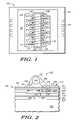
- FIG. 1is top view of one embodiment of a die including an inductor according to the present invention.
- FIG. 2is a partial side view of one embodiment of a die and inductor according to the present invention.
- FIG. 3is a top view of one embodiment of a transformer according to the present invention.
- FIG. 4is a top view of one embodiment of an inductor according to the present invention.
- FIG. 5is a perspective view of one embodiment of an inductor according to the present invention.
- FIG. 6is a flow diagram of one embodiment of making die with an inductive device according to the present invention.
- FIG. 1is a top view of a integrated circuit die according to the present invention.
- An inductor 105is located on a top side 131 of die 101 .
- Inductor 105includes a first set of bond wires (e.g. 113 ) including a portion located between a core 109 of magnetic material and the top side 131 of die 101 and a second set of bonding wires e.g. 111 including a portion located over core 109 .
- core 109is made of a ferrite material, but may include other types of magnetic material in other embodiments, e.g. ferromagnetic material.
- Each of the bond wires of the first and second setsare bonded to a pair of bond pads (e.g. 117 and 119 for bond wire 111 ) and function as segments of a coil around core 109 of inductor 105 .
- Bond wires 111 and 113are made of a conductive material such as e.g. gold, copper, or aluminum.
- Bond padsare located on the top side 131 of die 101 for providing external coupling of the circuitry (not shown) of die 101 . These bond pads may be wire bonded to bond pads of a package substrate (not shown) of which die 101 is implemented.
- FIG. 2is a partial side cross sectional view of die 101 and inductor 105 .
- bond wire 111extends over core 109 and is bonded to bond pad 117 and bond pad 119 .
- Bond wire 113has a lower profile than bond wire 111 , extends between core 109 and die 101 , and is bonded to pad 117 and pad 116 .
- core 109is attached to die 101 with insulative epoxy 142 that runs the length of core 109 .
- the bond wires of the first set(e.g. 113 ) extend through insulative epoxy 142 .
- Die 101includes a substrate 225 and a plurality of interconnect layers ( 223 , 221 , 219 , 217 , 215 , and 213 ) formed over substrate 225 .
- Substrate 225is made of silicon or other type of semiconductor material (e.g. GaAs).
- Devicessuch as transistors and diodes (not shown) are formed in substrate 225 to implement active circuitry of die 101 .
- the plurality of interconnect layersinclude conductive structures such as metal interconnects (e.g. 233 ) and conductive vias (e.g. 235 ).
- a passivation layer 211is located over the metal layer 213 .
- An aluminum shield 141is formed over passivation layer 211 and includes a portion 241 located beneath core 109 .
- Shield 141provide shielding to decrease magnetic coupling from inductor 105 with the circuitry in substrate 225 and conductive structures in the interconnect layers.
- Shield 141is electrically isolated from the bond pads (e.g. 117 , 119 , and 135 ).
- insulative epoxy 142covers portion 241 of shield 141 under core 109 to aid in the isolation of the bond wires from shield 141 .
- Providing a shield between an inductive device and diemay allow for conductive structures to be implemented in the interconnect layers beneath inductor 105 thereby allowing for the implementation of active circuitry in substrate 225 below inductor 105 .
- Bond pads 117 and 119are formed on a passivation layer 211 .
- Bond pad 116is formed over and is in electrical contact with a conductive structure 227 of metal layer 213 through an opening in passivation layer 211 .
- the bond pads ( 117 , 116 , 119 , and 135 ) and shield 141are formed from a patterned aluminum layer formed over passivation layer 221 .
- the bond pads and shield 141are made of other types of conductive material (e.g. copper).
- a barrier layer(not shown) may be located between bond pads (e.g. 116 ) and conductive structures (e.g. 227 ) of metal layer 213 .
- inductor 105is coupled to active circuitry in substrate 225 via pad 116 , conductive structure 227 in metal layer 213 , conductive vias 229 and 231 in via layer 215 , conductive structure 233 in metal layer 217 , conductive via 235 in via layer 219 , conductive structure 232 in layer 221 , and contact 239 in contact layer 223 .
- the conductive structures in the interconnect layersare made of a conductive material (e.g. copper, aluminum, and tungsten).
- the interconnect layers of die 101may include adhesive layers and/or diffusion barrier layers not shown.
- the bond pads at the end of the coile.g. 116 and 137
- FIG. 3is a top view of a transformer 301 formed on a substrate 302 .
- Transformer 301includes two sets of coils with each including a first set of bond wires including portions extending between the substrate 302 and magnetic core 303 and a second set of bond wires including portions extending over core 303 .
- Each of the bond wiresare bonded to bond pads (e.g. 307 ) located on substrate 302 .
- the first coilextends from bond pad 305 to bond pad 307 and the second coil extends from pad 311 to pad 309 .
- the first coilwould serve as the primary winding and the second coil would serve as the secondary winding.
- substrate 302is made of dielectric material and the bond pads (e.g. 305 ) are made of copper. In one embodiment, pads 307 , 309 , 305 and 311 are coupled to conductive vias (not shown) extending into substrate 302 for coupling to external coupling devices (e.g. solder balls, external bond pads) formed on the backside (not shown) of substrate 302 .
- substrate 302may be made of a dielectric material such as e.g. ceramic, glass, FR4, or bismalemide triazine. In other embodiments, the substrate may be made of a conductive material e.g. where the substrate is a lead frame.
- transformer 301 and substrate 302are encapsulated to form a stand alone inductor.
- inductor 301is formed on a substrate in which an IC die (not shown) is attached (e.g. either adjacent to or on the opposite side of substrate 302 ). In such embodiments, the die, substrate, and transformer are encapsulated.
- core 109 and core 303each have a cylindrical shape.
- coresmay have other shapes in other embodiments, such as e.g. a bar, toroid, and a square or rectangular frame with a rectangular cross section or circular cross section.
- FIG. 4is a top view of an inductor 401 formed on a substrate 402 .
- the coil of inductor 401includes a first plurality of bond wires e.g. 407 having a portion extending between substrate 402 and core 403 and a second plurality of bond wires e.g. 405 having a higher profile and a portion extending over core 403 .
- the bond wires of the first and second setsare bonded to bond pads (e.g. 409 ) on substrate 402 .
- core 403is made of a magnetic material, has a ring form, and has a square cross section.
- core 403is attached in substrate 402 with an epoxy (not shown).
- the bond wires of the first set(e.g. 407 ) extend through the epoxy.
- FIG. 5is a perspective view of another embodiment of an inductive device.
- Core 509includes core magnetic material 521 surrounded by a coat of insulative material 519 .
- Core 509is attached to substrate 502 with the use of standoffs 503 and 504 .
- Standoffs 503 and 504provide a predetermined clearance between the top side of substrate 502 and core 509 where bond wires (e.g. 507 ) pass from bond pads (e.g. 505 ) on a first side of core 509 to bond pads 522 on the other side of core 509 .
- bond wirese.g. 507
- standoffs 503 and 504are attached to substrate 502 prior to the bonding of the first set of bond wires (e.g. 507 ) with core 509 being attached thereafter. In another embodiment, standoffs 503 and 504 are attached to substrate 502 after the first set of bond wires (e.g. 507 ) are attached. In another embodiment, standoffs 503 and 504 are first attached to core 509 . Then the core/standoff assembly is attached to substrate 502 after the bonding of the first set of bond wires (e.g. 507 ).
- core material 521is ferromagnetic.
- An insulative coating 519coats core material 521 to electrically isolate core material 521 (which is electrically conductive) from the uninsulative bond wires.
- Providing a conductive coremay provide an inductive device with a higher permeability thereby providing a higher inductance.
- Other inductive devicesmay include insulated bond wires and a ferromagnetic core with no insulative coating.
- substrate 502is made of a dielectric material.
- standoffs 503 and 504may be attached to the top of a die (e.g. 101 ).
- FIG. 6sets forth one embodiment for making an inductive device according to the present invention.
- the bond pads and a shielde.g. 141
- the bond pads and a shieldare formed over a substrate.
- an aluminum layeris deposited on passivation layer 211 and then patterned to form the bond pads (e.g. 117 , 119 , and 116 ) and aluminum shield 141 .
- the first set of bond wires having the lower profileare bonded to the bond pads.
- a coreis mounted over the bond wires (e.g. 113 ).
- the coreis attached to the top of the die (e.g. 101 ) with insulative epoxy (e.g. 142 ) wherein the bond wires of the first set extend through the insulative epoxy.
- the second set of bond wiresare bonded to extend over the core.
- the inductor and substrateare then encapsulated.
- the inductor and dieare attached to a package substrate wherein bond pads of the die (and bond pads of the inductor in some embodiments) are bonded to bond pads of the package substrate. The entire package is then encapsulated.
- test runs of a packaged electronic devicemay be constructed and measurements made to determine the inductance of the inductive device. From these measurements, inductive devices on subsequently built devices may be adjusted to tune the inductance. For example, subsequent inductive devices may be constructed with less bond wires to reduce the effective length of the coil, and thereby the inductance of the inductive device.
- Providing an inductive device with bond wires extending between a substrate and coremay advantageously allow for a more dense placement of conductors extending between the core and the substrate over an inductive device having only traces extending between the core and substrate. Providing for a more dense placement may advantageously allow the inductive device to occupy less space. Furthermore, utilization of bond wires beneath the core and substrate of an inductive device may allow for placement of a shield between the substrate and core which may include at least portions formed in the same layer as the bond pads.
- a transformer similar to transformer 301 of FIG. 3may be attached to an IC die (e.g. 101 ).
- a transformer similar to transformer 301may be attached to a substrate 302 with standoffs (e.g. 503 and 504 ).
- an inductive devicein one embodiment, includes a core coupled to a substrate and a conductive coil surrounding the core.
- the coilcomprises segments formed from a first plurality of bond wires and a second plurality of bond wires.
- the first plurality of bond wiresextends between the core and the substrate.
- Each of the first plurality of bond wiresis coupled to two of a plurality of wire bond pads.
- the second plurality of bond wiresextends over the core and is coupled between two of the plurality of wire bond pads.
- a method for forming an inductive devicecomprises attaching a first plurality of bond wires between first pairs of a plurality of wire bond pads, positioning a core over the first plurality of bond wires, and attaching a second plurality of bond wires between second pairs of the plurality of wire bond pads.
- the second plurality of bond wiresextends over the core.
Landscapes
- Engineering & Computer Science (AREA)
- Power Engineering (AREA)
- Microelectronics & Electronic Packaging (AREA)
- Physics & Mathematics (AREA)
- Condensed Matter Physics & Semiconductors (AREA)
- General Physics & Mathematics (AREA)
- Computer Hardware Design (AREA)
- Manufacturing & Machinery (AREA)
- Coils Or Transformers For Communication (AREA)
- Semiconductor Integrated Circuits (AREA)
Abstract
Description
Claims (26)
Priority Applications (1)
| Application Number | Priority Date | Filing Date | Title |
|---|---|---|---|
| US10/729,531US6998952B2 (en) | 2003-12-05 | 2003-12-05 | Inductive device including bond wires |
Applications Claiming Priority (1)
| Application Number | Priority Date | Filing Date | Title |
|---|---|---|---|
| US10/729,531US6998952B2 (en) | 2003-12-05 | 2003-12-05 | Inductive device including bond wires |
Publications (2)
| Publication Number | Publication Date |
|---|---|
| US20050122198A1 US20050122198A1 (en) | 2005-06-09 |
| US6998952B2true US6998952B2 (en) | 2006-02-14 |
Family
ID=34633966
Family Applications (1)
| Application Number | Title | Priority Date | Filing Date |
|---|---|---|---|
| US10/729,531Expired - LifetimeUS6998952B2 (en) | 2003-12-05 | 2003-12-05 | Inductive device including bond wires |
Country Status (1)
| Country | Link |
|---|---|
| US (1) | US6998952B2 (en) |
Cited By (65)
| Publication number | Priority date | Publication date | Assignee | Title |
|---|---|---|---|---|
| US20060097831A1 (en)* | 2004-11-10 | 2006-05-11 | Lotfi Ashraf W | Power module |
| US20060097833A1 (en)* | 2004-11-10 | 2006-05-11 | Lotfi Ashraf W | Encapsulated package for a magnetic device |
| US20060096088A1 (en)* | 2004-11-10 | 2006-05-11 | Lotfi Ashraf W | Method of manufacturing an encapsulated package for a magnetic device |
| US20060096087A1 (en)* | 2004-11-10 | 2006-05-11 | Lotfi Ashraf W | Method of manufacturing a power module |
| US20070075815A1 (en)* | 2005-10-05 | 2007-04-05 | Lotfi Ashraf W | Method of forming a magnetic device having a conductive clip |
| US20070074386A1 (en)* | 2005-10-05 | 2007-04-05 | Lotfi Ashraf W | Method of forming a power module with a magnetic device having a conductive clip |
| US20070075817A1 (en)* | 2005-10-05 | 2007-04-05 | Lotfi Ashraf W | Magnetic device having a conductive clip |
| US20070075816A1 (en)* | 2005-10-05 | 2007-04-05 | Lotfi Ashraf W | Power module with a magnetic device having a conductive clip |
| US20070234554A1 (en)* | 2006-04-06 | 2007-10-11 | Cheng-Chou Hung | Method for fabricating a transformer integrated with a semiconductor structure |
| US20080079115A1 (en)* | 2006-09-29 | 2008-04-03 | Freescale Semiconductor, Inc. | Electronic device including an inductor and a process of forming the same |
| US20090066300A1 (en)* | 2007-09-10 | 2009-03-12 | Lotfi Ashraf W | Power Converter Employing a Micromagnetic Device |
| US20090068761A1 (en)* | 2007-09-10 | 2009-03-12 | Lotfi Ashraf W | Method of Forming a Micromagnetic Device |
| US20090068400A1 (en)* | 2007-09-10 | 2009-03-12 | Lotfi Ashraf W | Micromagnetic Device and Method of Forming the Same |
| US20090066467A1 (en)* | 2007-09-10 | 2009-03-12 | Lotfi Ashraf W | Micromagnetic Device and Method of Forming the Same |
| US20090134503A1 (en)* | 2007-11-23 | 2009-05-28 | Tao Feng | Semiconductor power device package having a lead frame-based integrated inductor |
| US20090160596A1 (en)* | 2007-12-19 | 2009-06-25 | Delta Electronics, Inc. | Magnetic device |
| US20090160595A1 (en)* | 2007-11-23 | 2009-06-25 | Tao Feng | Compact Power Semiconductor Package and Method with Stacked Inductor and Integrated Circuit Die |
| US20090167477A1 (en)* | 2007-11-23 | 2009-07-02 | Tao Feng | Compact Inductive Power Electronics Package |
| US20090201115A1 (en)* | 2008-02-13 | 2009-08-13 | Sajol Ghoshal | Inductance element in an integrated circuit package |
| US20100084750A1 (en)* | 2008-10-02 | 2010-04-08 | Lotfi Ashraf W | Module having a stacked passive element and method of forming the same |
| US20100087036A1 (en)* | 2008-10-02 | 2010-04-08 | Lotfi Ashraf W | Module having a stacked passive element and method of forming the same |
| US20100164449A1 (en)* | 2008-12-29 | 2010-07-01 | Mirmira Ramarao Dwarakanath | Power Converter with a Dynamically Configurable Controller and Output Filter |
| US7751164B1 (en) | 2003-01-29 | 2010-07-06 | Marvell International Ltd. | Electrostatic discharge protection circuit |
| US20100214746A1 (en)* | 2008-10-02 | 2010-08-26 | Lotfi Ashraf W | Module Having a Stacked Magnetic Device and Semiconductor Device and Method of Forming the Same |
| US20100212150A1 (en)* | 2008-10-02 | 2010-08-26 | Lotfi Ashraf W | Module Having a Stacked Magnetic Device and Semiconductor Device and Method of Forming the Same |
| US20100225434A1 (en)* | 2009-03-03 | 2010-09-09 | Freescale Semiconductor, Inc. | Stacked device assembly with integrated coil and method of forming same |
| US7884696B2 (en) | 2007-11-23 | 2011-02-08 | Alpha And Omega Semiconductor Incorporated | Lead frame-based discrete power inductor |
| US7939864B1 (en)* | 2010-06-01 | 2011-05-10 | Nxp B.V. | Inductive bond-wire circuit |
| US20110152604A1 (en)* | 2009-12-23 | 2011-06-23 | Hull Jr Raymond J | Intravaginal incontinence device |
| US8018315B2 (en) | 2007-09-10 | 2011-09-13 | Enpirion, Inc. | Power converter employing a micromagnetic device |
| US8133529B2 (en) | 2007-09-10 | 2012-03-13 | Enpirion, Inc. | Method of forming a micromagnetic device |
| US20130229255A1 (en)* | 2012-03-05 | 2013-09-05 | Delta Electronics, Inc. | Network transformer module and magnetic element thereof |
| US8541991B2 (en) | 2008-04-16 | 2013-09-24 | Enpirion, Inc. | Power converter with controller operable in selected modes of operation |
| US8686698B2 (en) | 2008-04-16 | 2014-04-01 | Enpirion, Inc. | Power converter with controller operable in selected modes of operation |
| US20140092574A1 (en)* | 2012-09-28 | 2014-04-03 | Uwe Zillmann | Integrated voltage regulators with magnetically enhanced inductors |
| US8692532B2 (en) | 2008-04-16 | 2014-04-08 | Enpirion, Inc. | Power converter with controller operable in selected modes of operation |
| US8867295B2 (en) | 2010-12-17 | 2014-10-21 | Enpirion, Inc. | Power converter for a memory module |
| US8976561B2 (en) | 2012-11-14 | 2015-03-10 | Power Integrations, Inc. | Switch mode power converters using magnetically coupled galvanically isolated lead frame communication |
| US9019728B2 (en) | 2013-03-08 | 2015-04-28 | Power Integrations, Inc. | Power converter output voltage clamp and supply terminal |
| US9035435B2 (en) | 2012-11-14 | 2015-05-19 | Power Integrations, Inc. | Magnetically coupled galvanically isolated communication using lead frame |
| US9071146B2 (en) | 2013-03-13 | 2015-06-30 | Power Integrations, Inc. | AC voltage sensor with low power consumption |
| US9087713B2 (en) | 2012-10-12 | 2015-07-21 | Power Integrations, Inc. | Semiconductor device with shared region |
| US9136765B2 (en) | 2013-03-08 | 2015-09-15 | Power Integrations, Inc. | Techniques for controlling a power converter using multiple controllers |
| US9166575B2 (en) | 2013-03-08 | 2015-10-20 | Power Integrations, Inc. | Low threshold voltage comparator |
| US9166486B2 (en) | 2013-03-08 | 2015-10-20 | Power Integrations, Inc. | Power converter using multiple controllers |
| US9178411B2 (en) | 2013-01-22 | 2015-11-03 | Power Integrations, Inc. | Charging circuit for a power converter controller |
| US9246390B2 (en) | 2008-04-16 | 2016-01-26 | Enpirion, Inc. | Power converter with controller operable in selected modes of operation |
| US9246392B2 (en) | 2013-03-13 | 2016-01-26 | Power Integrations, Inc. | Switched mode power converter controller with ramp time modulation |
| US9276479B2 (en) | 2013-01-22 | 2016-03-01 | Power Integrations, Inc. | Receive circuit for use in a power converter |
| US9331587B2 (en) | 2013-01-22 | 2016-05-03 | Power Integrations, Inc. | Power converter controller with multiple power sources |
| US9349717B2 (en) | 2012-11-14 | 2016-05-24 | Power Integrations, Inc. | Noise cancellation for a magnetically coupled communication link utilizing a lead frame |
| US9374011B2 (en) | 2013-01-22 | 2016-06-21 | Power Integrations, Inc. | Secondary controller for use in synchronous flyback converter |
| US9401657B2 (en) | 2013-03-13 | 2016-07-26 | Power Integrations, Inc. | Input voltage sensor responsive to load conditions |
| US9509217B2 (en) | 2015-04-20 | 2016-11-29 | Altera Corporation | Asymmetric power flow controller for a power converter and method of operating the same |
| US9548714B2 (en) | 2008-12-29 | 2017-01-17 | Altera Corporation | Power converter with a dynamically configurable controller and output filter |
| US9761553B2 (en)* | 2012-10-19 | 2017-09-12 | Taiwan Semiconductor Manufacturing Company Limited | Inductor with conductive trace |
| US9928954B2 (en)* | 2014-08-28 | 2018-03-27 | Ampleon Netherlands B.V. | Transformer |
| US10243442B1 (en) | 2017-11-22 | 2019-03-26 | Power Integrations, Inc. | Controller with frequency to on-time converter |
| US20200066659A1 (en)* | 2018-08-21 | 2020-02-27 | Intel Corporation | Wirebond and leadframe magnetic inductors |
| US10840005B2 (en) | 2013-01-25 | 2020-11-17 | Vishay Dale Electronics, Llc | Low profile high current composite transformer |
| US10854367B2 (en) | 2016-08-31 | 2020-12-01 | Vishay Dale Electronics, Llc | Inductor having high current coil with low direct current resistance |
| US10923417B2 (en) | 2017-04-26 | 2021-02-16 | Taiwan Semiconductor Manufacturing Company Limited | Integrated fan-out package with 3D magnetic core inductor |
| US10998124B2 (en) | 2016-05-06 | 2021-05-04 | Vishay Dale Electronics, Llc | Nested flat wound coils forming windings for transformers and inductors |
| US11948724B2 (en) | 2021-06-18 | 2024-04-02 | Vishay Dale Electronics, Llc | Method for making a multi-thickness electro-magnetic device |
| USD1034462S1 (en) | 2021-03-01 | 2024-07-09 | Vishay Dale Electronics, Llc | Inductor package |
Families Citing this family (18)
| Publication number | Priority date | Publication date | Assignee | Title |
|---|---|---|---|---|
| DE602005020005D1 (en)* | 2005-09-09 | 2010-04-29 | St Microelectronics Srl | Inductive arrangement |
| US7453142B2 (en)* | 2005-12-05 | 2008-11-18 | Texas Instruments Incorporated | System and method for implementing transformer on package substrate |
| US7719112B2 (en)* | 2006-08-07 | 2010-05-18 | University Of Central Florida Research Foundation, Inc. | On-chip magnetic components |
| US8064211B2 (en)* | 2006-08-31 | 2011-11-22 | Tdk Corporation | Passive component and electronic component module |
| US7952460B2 (en)* | 2006-11-14 | 2011-05-31 | Nxp B.V. | Manufacturing of an electronic circuit having an inductance |
| US8389868B2 (en)* | 2007-12-31 | 2013-03-05 | Texas Instruments Incorporated | Packaged integrated circuits having inductors and methods to form inductors in packaged integrated circuits |
| US8325002B2 (en)* | 2010-05-27 | 2012-12-04 | Advanced Semiconductor Engineering, Inc. | Power inductor structure |
| EP2461335B1 (en)* | 2010-12-03 | 2015-09-23 | Nxp B.V. | Bond wire transformer |
| DE102011086403A1 (en)* | 2011-11-15 | 2013-05-16 | Würth Elektronik eiSos Gmbh & Co. KG | inductance component |
| JP5958548B2 (en)* | 2012-10-04 | 2016-08-02 | 愛知製鋼株式会社 | Magneto-impedance element and manufacturing method thereof |
| US20140203902A1 (en)* | 2013-01-18 | 2014-07-24 | Geoffrey D. Shippee | Cards, devices, electromagnetic field generators and methods of manufacturing electromagnetic field generators |
| EP2992606B1 (en)* | 2013-05-03 | 2019-07-31 | Skyworks Solutions, Inc. | Coupled resonator on-die filters for wifi applications |
| TWI544668B (en)* | 2015-04-07 | 2016-08-01 | 矽品精密工業股份有限公司 | Electronic device |
| WO2016209245A1 (en) | 2015-06-25 | 2016-12-29 | Intel IP Corporation | Vertical inductor for wlcsp |
| JP2018019002A (en)* | 2016-07-29 | 2018-02-01 | 株式会社新川 | Microcoil and method for forming the same |
| US11380632B2 (en)* | 2018-04-27 | 2022-07-05 | Taiwan Semiconductor Manufacturing Company Ltd. | Semiconductor package device with integrated inductor and manufacturing method thereof |
| US11527489B2 (en) | 2018-06-29 | 2022-12-13 | Intel Corporation | Apparatus and system with package stiffening magnetic inductor core and methods of making the same |
| US20240038439A1 (en)* | 2022-07-28 | 2024-02-01 | Qualcomm Incorporated | Inductor packages employing wire bonds over a lead frame to form integrated inductor(s), and related integrated circuit (ic) packages and fabrication methods |
Citations (31)
| Publication number | Priority date | Publication date | Assignee | Title |
|---|---|---|---|---|
| US3263191A (en)* | 1964-06-30 | 1966-07-26 | Edward N Arvonio | Broad band toroid r.f. transformer |
| US3614554A (en)* | 1968-10-24 | 1971-10-19 | Texas Instruments Inc | Miniaturized thin film inductors for use in integrated circuits |
| US4103267A (en)* | 1977-06-13 | 1978-07-25 | Burr-Brown Research Corporation | Hybrid transformer device |
| US4524342A (en)* | 1981-12-28 | 1985-06-18 | Allied Corporation | Toroidal core electromagnetic device |
| US4806895A (en)* | 1987-10-08 | 1989-02-21 | Zenith Electronics Corporation | Toroidal coil mount |
| US5140706A (en)* | 1989-03-09 | 1992-08-18 | Murata Manufacturing Co., Ltd. | Transmission-line transformer device for double-balanced miner |
| US5425167A (en)* | 1991-05-31 | 1995-06-20 | Sumitomo Electric Industries, Ltd. | Method of making a transformer for monolithic microwave integrated circuit |
| US5425166A (en)* | 1993-06-01 | 1995-06-20 | Eaton Corporation | Current transformer using a laminated toroidal core structure and a lead frame |
| US5428245A (en) | 1994-05-06 | 1995-06-27 | National Semiconductor Corporation | Lead frame including an inductor or other such magnetic component |
| US5543773A (en)* | 1990-09-07 | 1996-08-06 | Electrotech Instruments Limited | Transformers and coupled inductors with optimum interleaving of windings |
| US5640127A (en) | 1995-11-07 | 1997-06-17 | Tektronix, Inc. | Input protection for high bandwidth amplifier |
| US5767563A (en)* | 1995-12-22 | 1998-06-16 | Micron Technology, Inc. | Inductor formed at least partially in a substrate |
| US5886393A (en) | 1997-11-07 | 1999-03-23 | National Semiconductor Corporation | Bonding wire inductor for use in an integrated circuit package and method |
| US5905418A (en) | 1997-02-12 | 1999-05-18 | Oki Electric Industry Co., Ltd. | Surface-acoustic-wave filters with poles of attenuation created by impedance circuits |
| US5945880A (en) | 1997-01-11 | 1999-08-31 | Mitel Semiconductor Limited | Low noise amplifier |
| US5963110A (en) | 1997-10-16 | 1999-10-05 | Fujitsu Limited | Equalizing filter and control method for signal equalization |
| US6194774B1 (en)* | 1999-03-10 | 2001-02-27 | Samsung Electronics Co., Ltd. | Inductor including bonding wires |
| EP1202296A1 (en) | 2000-10-27 | 2002-05-02 | Xerox Corporation | Out-of-plane microcoil using bonding wires and method for making |
| US6417755B1 (en) | 2000-08-25 | 2002-07-09 | Conexant Systems, Inc. | Method for fabrication of high inductance inductors and related structure |
| US6427315B1 (en) | 1996-08-23 | 2002-08-06 | Murata Manufacturing Co., Ltd. | Coil component and manufacturing method for the same |
| US6437653B1 (en) | 2000-09-28 | 2002-08-20 | Sun Microsystems, Inc. | Method and apparatus for providing a variable inductor on a semiconductor chip |
| US6452473B1 (en) | 1999-09-17 | 2002-09-17 | Fdk Corporation | Multilayer inductor and method of manufacturing the same |
| US6456183B1 (en) | 1999-02-26 | 2002-09-24 | Memscap And Planhead-Silmag Phs | Inductor for integrated circuit |
| US6466122B1 (en) | 1988-09-30 | 2002-10-15 | Kabushiki Kaisha Toshiba | Planar inductor |
| US6472257B2 (en) | 1997-10-23 | 2002-10-29 | Stmicroelectronics S.R.L. | High quality factor, integrated inductor and production method thereof |
| US6478975B1 (en) | 1999-08-23 | 2002-11-12 | Hynix Semiconductor Inc. | Inductor and fabricating method thereof |
| US6480086B1 (en) | 1999-12-20 | 2002-11-12 | Advanced Micro Devices, Inc. | Inductor and transformer formed with multi-layer coil turns fabricated on an integrated circuit substrate |
| US6480087B1 (en) | 1999-09-17 | 2002-11-12 | Murata Manufacturing Co., Ltd. | Laminated inductor array |
| US6483413B1 (en) | 1999-09-03 | 2002-11-19 | Murata Manufacturing Co., Ltd. | Laminated inductor |
| US20030031339A1 (en)* | 2000-01-13 | 2003-02-13 | Marshall Bowen F. | Packaging and rf shielding for telecoils |
| US6586309B1 (en) | 2000-04-24 | 2003-07-01 | Chartered Semiconductor Manufacturing Ltd. | High performance RF inductors and transformers using bonding technique |
- 2003
- 2003-12-05USUS10/729,531patent/US6998952B2/ennot_activeExpired - Lifetime
Patent Citations (31)
| Publication number | Priority date | Publication date | Assignee | Title |
|---|---|---|---|---|
| US3263191A (en)* | 1964-06-30 | 1966-07-26 | Edward N Arvonio | Broad band toroid r.f. transformer |
| US3614554A (en)* | 1968-10-24 | 1971-10-19 | Texas Instruments Inc | Miniaturized thin film inductors for use in integrated circuits |
| US4103267A (en)* | 1977-06-13 | 1978-07-25 | Burr-Brown Research Corporation | Hybrid transformer device |
| US4524342A (en)* | 1981-12-28 | 1985-06-18 | Allied Corporation | Toroidal core electromagnetic device |
| US4806895A (en)* | 1987-10-08 | 1989-02-21 | Zenith Electronics Corporation | Toroidal coil mount |
| US6466122B1 (en) | 1988-09-30 | 2002-10-15 | Kabushiki Kaisha Toshiba | Planar inductor |
| US5140706A (en)* | 1989-03-09 | 1992-08-18 | Murata Manufacturing Co., Ltd. | Transmission-line transformer device for double-balanced miner |
| US5543773A (en)* | 1990-09-07 | 1996-08-06 | Electrotech Instruments Limited | Transformers and coupled inductors with optimum interleaving of windings |
| US5425167A (en)* | 1991-05-31 | 1995-06-20 | Sumitomo Electric Industries, Ltd. | Method of making a transformer for monolithic microwave integrated circuit |
| US5425166A (en)* | 1993-06-01 | 1995-06-20 | Eaton Corporation | Current transformer using a laminated toroidal core structure and a lead frame |
| US5428245A (en) | 1994-05-06 | 1995-06-27 | National Semiconductor Corporation | Lead frame including an inductor or other such magnetic component |
| US5640127A (en) | 1995-11-07 | 1997-06-17 | Tektronix, Inc. | Input protection for high bandwidth amplifier |
| US5767563A (en)* | 1995-12-22 | 1998-06-16 | Micron Technology, Inc. | Inductor formed at least partially in a substrate |
| US6427315B1 (en) | 1996-08-23 | 2002-08-06 | Murata Manufacturing Co., Ltd. | Coil component and manufacturing method for the same |
| US5945880A (en) | 1997-01-11 | 1999-08-31 | Mitel Semiconductor Limited | Low noise amplifier |
| US5905418A (en) | 1997-02-12 | 1999-05-18 | Oki Electric Industry Co., Ltd. | Surface-acoustic-wave filters with poles of attenuation created by impedance circuits |
| US5963110A (en) | 1997-10-16 | 1999-10-05 | Fujitsu Limited | Equalizing filter and control method for signal equalization |
| US6472257B2 (en) | 1997-10-23 | 2002-10-29 | Stmicroelectronics S.R.L. | High quality factor, integrated inductor and production method thereof |
| US5886393A (en) | 1997-11-07 | 1999-03-23 | National Semiconductor Corporation | Bonding wire inductor for use in an integrated circuit package and method |
| US6456183B1 (en) | 1999-02-26 | 2002-09-24 | Memscap And Planhead-Silmag Phs | Inductor for integrated circuit |
| US6194774B1 (en)* | 1999-03-10 | 2001-02-27 | Samsung Electronics Co., Ltd. | Inductor including bonding wires |
| US6478975B1 (en) | 1999-08-23 | 2002-11-12 | Hynix Semiconductor Inc. | Inductor and fabricating method thereof |
| US6483413B1 (en) | 1999-09-03 | 2002-11-19 | Murata Manufacturing Co., Ltd. | Laminated inductor |
| US6452473B1 (en) | 1999-09-17 | 2002-09-17 | Fdk Corporation | Multilayer inductor and method of manufacturing the same |
| US6480087B1 (en) | 1999-09-17 | 2002-11-12 | Murata Manufacturing Co., Ltd. | Laminated inductor array |
| US6480086B1 (en) | 1999-12-20 | 2002-11-12 | Advanced Micro Devices, Inc. | Inductor and transformer formed with multi-layer coil turns fabricated on an integrated circuit substrate |
| US20030031339A1 (en)* | 2000-01-13 | 2003-02-13 | Marshall Bowen F. | Packaging and rf shielding for telecoils |
| US6586309B1 (en) | 2000-04-24 | 2003-07-01 | Chartered Semiconductor Manufacturing Ltd. | High performance RF inductors and transformers using bonding technique |
| US6417755B1 (en) | 2000-08-25 | 2002-07-09 | Conexant Systems, Inc. | Method for fabrication of high inductance inductors and related structure |
| US6437653B1 (en) | 2000-09-28 | 2002-08-20 | Sun Microsystems, Inc. | Method and apparatus for providing a variable inductor on a semiconductor chip |
| EP1202296A1 (en) | 2000-10-27 | 2002-05-02 | Xerox Corporation | Out-of-plane microcoil using bonding wires and method for making |
Cited By (136)
| Publication number | Priority date | Publication date | Assignee | Title |
|---|---|---|---|---|
| US7751164B1 (en) | 2003-01-29 | 2010-07-06 | Marvell International Ltd. | Electrostatic discharge protection circuit |
| US8528190B2 (en) | 2004-11-10 | 2013-09-10 | Enpirion, Inc. | Method of manufacturing a power module |
| US20060097833A1 (en)* | 2004-11-10 | 2006-05-11 | Lotfi Ashraf W | Encapsulated package for a magnetic device |
| US20060096088A1 (en)* | 2004-11-10 | 2006-05-11 | Lotfi Ashraf W | Method of manufacturing an encapsulated package for a magnetic device |
| US20060096087A1 (en)* | 2004-11-10 | 2006-05-11 | Lotfi Ashraf W | Method of manufacturing a power module |
| US20060097831A1 (en)* | 2004-11-10 | 2006-05-11 | Lotfi Ashraf W | Power module |
| US20090065964A1 (en)* | 2004-11-10 | 2009-03-12 | Lotfi Ashraf W | Method of Manufacturing an Encapsulated Package for a Magnetic Device |
| US8043544B2 (en) | 2004-11-10 | 2011-10-25 | Enpirion, Inc. | Method of manufacturing an encapsulated package for a magnetic device |
| US7256674B2 (en)* | 2004-11-10 | 2007-08-14 | Enpirion, Inc. | Power module |
| US7276998B2 (en) | 2004-11-10 | 2007-10-02 | Enpirion, Inc. | Encapsulated package for a magnetic device |
| US7462317B2 (en) | 2004-11-10 | 2008-12-09 | Enpirion, Inc. | Method of manufacturing an encapsulated package for a magnetic device |
| US7426780B2 (en) | 2004-11-10 | 2008-09-23 | Enpirion, Inc. | Method of manufacturing a power module |
| US20070075817A1 (en)* | 2005-10-05 | 2007-04-05 | Lotfi Ashraf W | Magnetic device having a conductive clip |
| US20100176905A1 (en)* | 2005-10-05 | 2010-07-15 | Lotfi Ashraf W | Magnetic Device Having a Conductive Clip |
| US7688172B2 (en) | 2005-10-05 | 2010-03-30 | Enpirion, Inc. | Magnetic device having a conductive clip |
| US10304615B2 (en) | 2005-10-05 | 2019-05-28 | Enpirion, Inc. | Method of forming a power module with a magnetic device having a conductive clip |
| US20070075815A1 (en)* | 2005-10-05 | 2007-04-05 | Lotfi Ashraf W | Method of forming a magnetic device having a conductive clip |
| US8139362B2 (en) | 2005-10-05 | 2012-03-20 | Enpirion, Inc. | Power module with a magnetic device having a conductive clip |
| US20070075816A1 (en)* | 2005-10-05 | 2007-04-05 | Lotfi Ashraf W | Power module with a magnetic device having a conductive clip |
| US8631560B2 (en) | 2005-10-05 | 2014-01-21 | Enpirion, Inc. | Method of forming a magnetic device having a conductive clip |
| US8701272B2 (en) | 2005-10-05 | 2014-04-22 | Enpirion, Inc. | Method of forming a power module with a magnetic device having a conductive clip |
| US8384506B2 (en)* | 2005-10-05 | 2013-02-26 | Enpirion, Inc. | Magnetic device having a conductive clip |
| US20070074386A1 (en)* | 2005-10-05 | 2007-04-05 | Lotfi Ashraf W | Method of forming a power module with a magnetic device having a conductive clip |
| US7321285B2 (en)* | 2006-04-06 | 2008-01-22 | United Microelectronics Corp. | Method for fabricating a transformer integrated with a semiconductor structure |
| US20070234554A1 (en)* | 2006-04-06 | 2007-10-11 | Cheng-Chou Hung | Method for fabricating a transformer integrated with a semiconductor structure |
| US20070236320A1 (en)* | 2006-04-06 | 2007-10-11 | Cheng-Chou Hung | Method for fabricating a transformer integrated with a semiconductor structure |
| US7367113B2 (en) | 2006-04-06 | 2008-05-06 | United Microelectronics Corp. | Method for fabricating a transformer integrated with a semiconductor structure |
| US7619297B2 (en) | 2006-09-29 | 2009-11-17 | Freescale Semiconductor, Inc. | Electronic device including an inductor |
| US20090152676A1 (en)* | 2006-09-29 | 2009-06-18 | Freescale Semiconductor, Inc. | Electronic device including an inductor |
| US20080079115A1 (en)* | 2006-09-29 | 2008-04-03 | Freescale Semiconductor, Inc. | Electronic device including an inductor and a process of forming the same |
| US7524731B2 (en) | 2006-09-29 | 2009-04-28 | Freescale Semiconductor, Inc. | Process of forming an electronic device including an inductor |
| US8018315B2 (en) | 2007-09-10 | 2011-09-13 | Enpirion, Inc. | Power converter employing a micromagnetic device |
| US7920042B2 (en) | 2007-09-10 | 2011-04-05 | Enpirion, Inc. | Micromagnetic device and method of forming the same |
| US7544995B2 (en) | 2007-09-10 | 2009-06-09 | Enpirion, Inc. | Power converter employing a micromagnetic device |
| US9299489B2 (en) | 2007-09-10 | 2016-03-29 | Enpirion, Inc. | Micromagnetic device and method of forming the same |
| US8339232B2 (en) | 2007-09-10 | 2012-12-25 | Enpirion, Inc. | Micromagnetic device and method of forming the same |
| US20090066300A1 (en)* | 2007-09-10 | 2009-03-12 | Lotfi Ashraf W | Power Converter Employing a Micromagnetic Device |
| US8133529B2 (en) | 2007-09-10 | 2012-03-13 | Enpirion, Inc. | Method of forming a micromagnetic device |
| US20090066467A1 (en)* | 2007-09-10 | 2009-03-12 | Lotfi Ashraf W | Micromagnetic Device and Method of Forming the Same |
| US20090068761A1 (en)* | 2007-09-10 | 2009-03-12 | Lotfi Ashraf W | Method of Forming a Micromagnetic Device |
| US20110181383A1 (en)* | 2007-09-10 | 2011-07-28 | Lotfi Ashraf W | Micromagnetic Device and Method of Forming the Same |
| US8618900B2 (en) | 2007-09-10 | 2013-12-31 | Enpirion, Inc. | Micromagnetic device and method of forming the same |
| US20090068400A1 (en)* | 2007-09-10 | 2009-03-12 | Lotfi Ashraf W | Micromagnetic Device and Method of Forming the Same |
| US7952459B2 (en) | 2007-09-10 | 2011-05-31 | Enpirion, Inc. | Micromagnetic device and method of forming the same |
| US7955868B2 (en) | 2007-09-10 | 2011-06-07 | Enpirion, Inc. | Method of forming a micromagnetic device |
| US20110121934A1 (en)* | 2007-11-23 | 2011-05-26 | Hebert Francois | Lead Frame-based Discrete Power Inductor |
| US8217748B2 (en) | 2007-11-23 | 2012-07-10 | Alpha & Omega Semiconductor Inc. | Compact inductive power electronics package |
| US20090134503A1 (en)* | 2007-11-23 | 2009-05-28 | Tao Feng | Semiconductor power device package having a lead frame-based integrated inductor |
| US7884452B2 (en)* | 2007-11-23 | 2011-02-08 | Alpha And Omega Semiconductor Incorporated | Semiconductor power device package having a lead frame-based integrated inductor |
| US7884696B2 (en) | 2007-11-23 | 2011-02-08 | Alpha And Omega Semiconductor Incorporated | Lead frame-based discrete power inductor |
| CN101861648B (en)* | 2007-11-23 | 2012-08-29 | 万国半导体有限公司 | Semiconductor power device package having a lead frame-based integrated inductor |
| US7868431B2 (en)* | 2007-11-23 | 2011-01-11 | Alpha And Omega Semiconductor Incorporated | Compact power semiconductor package and method with stacked inductor and integrated circuit die |
| US20090167477A1 (en)* | 2007-11-23 | 2009-07-02 | Tao Feng | Compact Inductive Power Electronics Package |
| US20090160595A1 (en)* | 2007-11-23 | 2009-06-25 | Tao Feng | Compact Power Semiconductor Package and Method with Stacked Inductor and Integrated Circuit Die |
| US8058961B2 (en) | 2007-11-23 | 2011-11-15 | Alpha And Omega Semiconductor Incorporated | Lead frame-based discrete power inductor |
| US20090160596A1 (en)* | 2007-12-19 | 2009-06-25 | Delta Electronics, Inc. | Magnetic device |
| US7889047B2 (en)* | 2007-12-19 | 2011-02-15 | Delta Electronics Inc. | Magnetic device |
| US20090201115A1 (en)* | 2008-02-13 | 2009-08-13 | Sajol Ghoshal | Inductance element in an integrated circuit package |
| US9246390B2 (en) | 2008-04-16 | 2016-01-26 | Enpirion, Inc. | Power converter with controller operable in selected modes of operation |
| US8692532B2 (en) | 2008-04-16 | 2014-04-08 | Enpirion, Inc. | Power converter with controller operable in selected modes of operation |
| US8541991B2 (en) | 2008-04-16 | 2013-09-24 | Enpirion, Inc. | Power converter with controller operable in selected modes of operation |
| US8686698B2 (en) | 2008-04-16 | 2014-04-01 | Enpirion, Inc. | Power converter with controller operable in selected modes of operation |
| US20100087036A1 (en)* | 2008-10-02 | 2010-04-08 | Lotfi Ashraf W | Module having a stacked passive element and method of forming the same |
| US9054086B2 (en) | 2008-10-02 | 2015-06-09 | Enpirion, Inc. | Module having a stacked passive element and method of forming the same |
| US8339802B2 (en) | 2008-10-02 | 2012-12-25 | Enpirion, Inc. | Module having a stacked magnetic device and semiconductor device and method of forming the same |
| US8266793B2 (en) | 2008-10-02 | 2012-09-18 | Enpirion, Inc. | Module having a stacked magnetic device and semiconductor device and method of forming the same |
| US8153473B2 (en) | 2008-10-02 | 2012-04-10 | Empirion, Inc. | Module having a stacked passive element and method of forming the same |
| US20100214746A1 (en)* | 2008-10-02 | 2010-08-26 | Lotfi Ashraf W | Module Having a Stacked Magnetic Device and Semiconductor Device and Method of Forming the Same |
| US20100084750A1 (en)* | 2008-10-02 | 2010-04-08 | Lotfi Ashraf W | Module having a stacked passive element and method of forming the same |
| US20100212150A1 (en)* | 2008-10-02 | 2010-08-26 | Lotfi Ashraf W | Module Having a Stacked Magnetic Device and Semiconductor Device and Method of Forming the Same |
| US9548714B2 (en) | 2008-12-29 | 2017-01-17 | Altera Corporation | Power converter with a dynamically configurable controller and output filter |
| US20100164449A1 (en)* | 2008-12-29 | 2010-07-01 | Mirmira Ramarao Dwarakanath | Power Converter with a Dynamically Configurable Controller and Output Filter |
| US8698463B2 (en) | 2008-12-29 | 2014-04-15 | Enpirion, Inc. | Power converter with a dynamically configurable controller based on a power conversion mode |
| US7868729B2 (en) | 2009-03-03 | 2011-01-11 | Freescale Semiconductor, Inc. | Stacked device assembly with integrated coil and method of forming same |
| US20100225434A1 (en)* | 2009-03-03 | 2010-09-09 | Freescale Semiconductor, Inc. | Stacked device assembly with integrated coil and method of forming same |
| US20110152604A1 (en)* | 2009-12-23 | 2011-06-23 | Hull Jr Raymond J | Intravaginal incontinence device |
| US7939864B1 (en)* | 2010-06-01 | 2011-05-10 | Nxp B.V. | Inductive bond-wire circuit |
| US8867295B2 (en) | 2010-12-17 | 2014-10-21 | Enpirion, Inc. | Power converter for a memory module |
| US9627028B2 (en) | 2010-12-17 | 2017-04-18 | Enpirion, Inc. | Power converter for a memory module |
| US20130229255A1 (en)* | 2012-03-05 | 2013-09-05 | Delta Electronics, Inc. | Network transformer module and magnetic element thereof |
| US20140092574A1 (en)* | 2012-09-28 | 2014-04-03 | Uwe Zillmann | Integrated voltage regulators with magnetically enhanced inductors |
| US9921640B2 (en)* | 2012-09-28 | 2018-03-20 | Intel Corporation | Integrated voltage regulators with magnetically enhanced inductors |
| US9087713B2 (en) | 2012-10-12 | 2015-07-21 | Power Integrations, Inc. | Semiconductor device with shared region |
| US9761553B2 (en)* | 2012-10-19 | 2017-09-12 | Taiwan Semiconductor Manufacturing Company Limited | Inductor with conductive trace |
| US9035435B2 (en) | 2012-11-14 | 2015-05-19 | Power Integrations, Inc. | Magnetically coupled galvanically isolated communication using lead frame |
| US10224292B2 (en) | 2012-11-14 | 2019-03-05 | Power Integrations, Inc. | Noise cancellation for a magnetically coupled communication link utilizing a lead frame |
| US9831188B2 (en) | 2012-11-14 | 2017-11-28 | Power Integrations, Inc. | Noise cancellation for a magnetically coupled communication link utilizing a lead frame |
| US10079543B2 (en) | 2012-11-14 | 2018-09-18 | Power Intergrations, Inc. | Magnetically coupled galvanically isolated communication using lead frame |
| US9275946B2 (en) | 2012-11-14 | 2016-03-01 | Power Integrations, Inc. | Switch mode power converters using magnetically coupled galvanically isolated lead frame communication |
| US10361632B2 (en) | 2012-11-14 | 2019-07-23 | Power Integrations, Inc. | Magnetically coupled galvanically isolated communication using lead frame |
| US9331004B2 (en) | 2012-11-14 | 2016-05-03 | Power Integrations, Inc. | Magnetically coupled galvanically isolated communication using lead frame |
| US12401285B2 (en) | 2012-11-14 | 2025-08-26 | Power Integrations, Inc. | Magnetically coupled galvanically isolated communication using lead frame |
| US9349717B2 (en) | 2012-11-14 | 2016-05-24 | Power Integrations, Inc. | Noise cancellation for a magnetically coupled communication link utilizing a lead frame |
| US8976561B2 (en) | 2012-11-14 | 2015-03-10 | Power Integrations, Inc. | Switch mode power converters using magnetically coupled galvanically isolated lead frame communication |
| US11088621B2 (en) | 2013-01-22 | 2021-08-10 | Power Integrations, Inc. | Secondary controller for use in synchronous flyback converter |
| US9374011B2 (en) | 2013-01-22 | 2016-06-21 | Power Integrations, Inc. | Secondary controller for use in synchronous flyback converter |
| US9331587B2 (en) | 2013-01-22 | 2016-05-03 | Power Integrations, Inc. | Power converter controller with multiple power sources |
| US10243471B2 (en) | 2013-01-22 | 2019-03-26 | Power Integrations, Inc. | Power converter controller with multiple power sources |
| US9276479B2 (en) | 2013-01-22 | 2016-03-01 | Power Integrations, Inc. | Receive circuit for use in a power converter |
| US9178411B2 (en) | 2013-01-22 | 2015-11-03 | Power Integrations, Inc. | Charging circuit for a power converter controller |
| US11824453B2 (en) | 2013-01-22 | 2023-11-21 | Power Integrations, Inc. | Secondary controller for use in synchronous flyback converter |
| US10840005B2 (en) | 2013-01-25 | 2020-11-17 | Vishay Dale Electronics, Llc | Low profile high current composite transformer |
| US12154712B2 (en) | 2013-01-25 | 2024-11-26 | Vishay Dale Electronics, Llc | Method of forming an electromagnetic device |
| US9136765B2 (en) | 2013-03-08 | 2015-09-15 | Power Integrations, Inc. | Techniques for controlling a power converter using multiple controllers |
| US9019728B2 (en) | 2013-03-08 | 2015-04-28 | Power Integrations, Inc. | Power converter output voltage clamp and supply terminal |
| US9929656B2 (en) | 2013-03-08 | 2018-03-27 | Power Integrations, Inc. | Power converter using multiple controllers |
| US11309800B2 (en) | 2013-03-08 | 2022-04-19 | Power Integrations, Inc. | Techniques for controlling a power converter using multiple controllers |
| US9166575B2 (en) | 2013-03-08 | 2015-10-20 | Power Integrations, Inc. | Low threshold voltage comparator |
| US9166486B2 (en) | 2013-03-08 | 2015-10-20 | Power Integrations, Inc. | Power converter using multiple controllers |
| US9627985B2 (en) | 2013-03-08 | 2017-04-18 | Power Integrations, Inc. | Power converter output voltage clamp and supply terminal |
| US9762129B2 (en) | 2013-03-08 | 2017-09-12 | Power Integrations, Inc. | Techniques for controlling a power converter using multiple controllers |
| US10230305B2 (en) | 2013-03-08 | 2019-03-12 | Power Integrations, Inc. | Techniques for controlling a power converter using multiple controllers |
| US11349398B2 (en) | 2013-03-13 | 2022-05-31 | Power Integrations, Inc | Switched mode power converter controller with ramp time modulation |
| US10158295B2 (en) | 2013-03-13 | 2018-12-18 | Power Integrations, Inc. | Switched mode power converter controller with ramp time modulation |
| US9837911B2 (en) | 2013-03-13 | 2017-12-05 | Power Integrations, Inc. | Switched mode power converter controller with ramp time modulation |
| US9401657B2 (en) | 2013-03-13 | 2016-07-26 | Power Integrations, Inc. | Input voltage sensor responsive to load conditions |
| US9071146B2 (en) | 2013-03-13 | 2015-06-30 | Power Integrations, Inc. | AC voltage sensor with low power consumption |
| US10811977B2 (en) | 2013-03-13 | 2020-10-20 | Power Integrations, Inc. | Switched mode power converter controller with ramp time modulation |
| US9246392B2 (en) | 2013-03-13 | 2016-01-26 | Power Integrations, Inc. | Switched mode power converter controller with ramp time modulation |
| US9866125B2 (en) | 2013-03-13 | 2018-01-09 | Power Integrations, Inc. | Input voltage sensor responsive to load conditions |
| US9928954B2 (en)* | 2014-08-28 | 2018-03-27 | Ampleon Netherlands B.V. | Transformer |
| US9509217B2 (en) | 2015-04-20 | 2016-11-29 | Altera Corporation | Asymmetric power flow controller for a power converter and method of operating the same |
| US10084380B2 (en) | 2015-04-20 | 2018-09-25 | Altera Corporation | Asymmetric power flow controller for a power converter and method of operating the same |
| US10998124B2 (en) | 2016-05-06 | 2021-05-04 | Vishay Dale Electronics, Llc | Nested flat wound coils forming windings for transformers and inductors |
| US11049638B2 (en) | 2016-08-31 | 2021-06-29 | Vishay Dale Electronics, Llc | Inductor having high current coil with low direct current resistance |
| US10854367B2 (en) | 2016-08-31 | 2020-12-01 | Vishay Dale Electronics, Llc | Inductor having high current coil with low direct current resistance |
| US11875926B2 (en) | 2016-08-31 | 2024-01-16 | Vishay Dale Electronics, Llc | Inductor having high current coil with low direct current resistance |
| US10923417B2 (en) | 2017-04-26 | 2021-02-16 | Taiwan Semiconductor Manufacturing Company Limited | Integrated fan-out package with 3D magnetic core inductor |
| US11688685B2 (en) | 2017-04-26 | 2023-06-27 | Taiwan Semiconductor Manufacturing Company Limited | Integrated fan-out package with 3D magnetic core inductor |
| US12272637B2 (en) | 2017-04-26 | 2025-04-08 | Taiwan Semiconductor Manufacturing Company Limited | Integrated fan-out package with 3D magnetic core inductor |
| US10243442B1 (en) | 2017-11-22 | 2019-03-26 | Power Integrations, Inc. | Controller with frequency to on-time converter |
| US11804456B2 (en)* | 2018-08-21 | 2023-10-31 | Intel Corporation | Wirebond and leadframe magnetic inductors |
| US20200066659A1 (en)* | 2018-08-21 | 2020-02-27 | Intel Corporation | Wirebond and leadframe magnetic inductors |
| USD1034462S1 (en) | 2021-03-01 | 2024-07-09 | Vishay Dale Electronics, Llc | Inductor package |
| USD1077746S1 (en) | 2021-03-01 | 2025-06-03 | Vishay Dale Electronics, Llc | Inductor package |
| US11948724B2 (en) | 2021-06-18 | 2024-04-02 | Vishay Dale Electronics, Llc | Method for making a multi-thickness electro-magnetic device |
Also Published As
| Publication number | Publication date |
|---|---|
| US20050122198A1 (en) | 2005-06-09 |
Similar Documents
| Publication | Publication Date | Title |
|---|---|---|
| US6998952B2 (en) | Inductive device including bond wires | |
| US10008318B2 (en) | System and method for integrated inductor | |
| US7280024B2 (en) | Integrated transformer structure and method of fabrication | |
| US9041505B2 (en) | System and method for a coreless transformer | |
| US12176285B2 (en) | Transformer guard trace | |
| US7986211B2 (en) | Inductor | |
| JP2018528620A (en) | Low profile package with passive devices | |
| US20180190573A1 (en) | Leadframe inductor | |
| US20130119511A1 (en) | Inductor having bond-wire and manufacturing method thereof | |
| US20230154873A1 (en) | Electronic package and manufacturing method thereof | |
| CN112992476B (en) | Transformer, and package module | |
| US11270937B2 (en) | Integrated inductor with magnetic mold compound | |
| US20230335511A1 (en) | Packaging Substrate | |
| EP1248297B1 (en) | Inductance element and semiconductor device | |
| US6833781B1 (en) | High Q inductor in multi-level interconnect | |
| TWI681414B (en) | Electronic module | |
| JPH10154795A (en) | Inductor on semiconductor chip and its manufacturing method | |
| CN108305855B (en) | Electronic package and substrate structure thereof | |
| CN117766510A (en) | Module structure and manufacturing method thereof | |
| US20160300660A1 (en) | Electronic device | |
| US20240290691A1 (en) | Electronic package and manufacturing method thereof | |
| KR102342732B1 (en) | Inductor device with improved q-factor using periodic metal pattern structure | |
| US20240282723A1 (en) | Integrated circuit (ic) package including an inductive device formed in a conductive routing region | |
| US20240120964A1 (en) | Packaged integrated circuit having package substrate with integrated isolation circuit | |
| WO2001013433A1 (en) | Spherical shaped integrated circuit utilizing an inductor |
Legal Events
| Date | Code | Title | Description |
|---|---|---|---|
| AS | Assignment | Owner name:MOTOROLA, INC., TEXAS Free format text:ASSIGNMENT OF ASSIGNORS INTEREST;ASSIGNORS:ZHOU, YAPING;DOWNEY, SUSAN H.;CHOPIN, SHEILA F.;AND OTHERS;REEL/FRAME:014773/0017;SIGNING DATES FROM 20031202 TO 20031203 | |
| AS | Assignment | Owner name:FREESCALE SEMICONDUCTOR, INC., TEXAS Free format text:ASSIGNMENT OF ASSIGNORS INTEREST;ASSIGNOR:MOTOROLA, INC;REEL/FRAME:015360/0718 Effective date:20040404 Owner name:FREESCALE SEMICONDUCTOR, INC.,TEXAS Free format text:ASSIGNMENT OF ASSIGNORS INTEREST;ASSIGNOR:MOTOROLA, INC;REEL/FRAME:015360/0718 Effective date:20040404 | |
| STCF | Information on status: patent grant | Free format text:PATENTED CASE | |
| AS | Assignment | Owner name:CITIBANK, N.A. AS COLLATERAL AGENT, NEW YORK Free format text:SECURITY AGREEMENT;ASSIGNORS:FREESCALE SEMICONDUCTOR, INC.;FREESCALE ACQUISITION CORPORATION;FREESCALE ACQUISITION HOLDINGS CORP.;AND OTHERS;REEL/FRAME:018855/0129 Effective date:20061201 Owner name:CITIBANK, N.A. AS COLLATERAL AGENT,NEW YORK Free format text:SECURITY AGREEMENT;ASSIGNORS:FREESCALE SEMICONDUCTOR, INC.;FREESCALE ACQUISITION CORPORATION;FREESCALE ACQUISITION HOLDINGS CORP.;AND OTHERS;REEL/FRAME:018855/0129 Effective date:20061201 | |
| CC | Certificate of correction | ||
| FPAY | Fee payment | Year of fee payment:4 | |
| AS | Assignment | Owner name:CITIBANK, N.A., AS COLLATERAL AGENT,NEW YORK Free format text:SECURITY AGREEMENT;ASSIGNOR:FREESCALE SEMICONDUCTOR, INC.;REEL/FRAME:024397/0001 Effective date:20100413 Owner name:CITIBANK, N.A., AS COLLATERAL AGENT, NEW YORK Free format text:SECURITY AGREEMENT;ASSIGNOR:FREESCALE SEMICONDUCTOR, INC.;REEL/FRAME:024397/0001 Effective date:20100413 | |
| FPAY | Fee payment | Year of fee payment:8 | |
| AS | Assignment | Owner name:CITIBANK, N.A., AS NOTES COLLATERAL AGENT, NEW YORK Free format text:SECURITY AGREEMENT;ASSIGNOR:FREESCALE SEMICONDUCTOR, INC.;REEL/FRAME:030633/0424 Effective date:20130521 Owner name:CITIBANK, N.A., AS NOTES COLLATERAL AGENT, NEW YOR Free format text:SECURITY AGREEMENT;ASSIGNOR:FREESCALE SEMICONDUCTOR, INC.;REEL/FRAME:030633/0424 Effective date:20130521 | |
| AS | Assignment | Owner name:CITIBANK, N.A., AS NOTES COLLATERAL AGENT, NEW YORK Free format text:SECURITY AGREEMENT;ASSIGNOR:FREESCALE SEMICONDUCTOR, INC.;REEL/FRAME:031591/0266 Effective date:20131101 Owner name:CITIBANK, N.A., AS NOTES COLLATERAL AGENT, NEW YOR Free format text:SECURITY AGREEMENT;ASSIGNOR:FREESCALE SEMICONDUCTOR, INC.;REEL/FRAME:031591/0266 Effective date:20131101 | |
| AS | Assignment | Owner name:FREESCALE SEMICONDUCTOR, INC., TEXAS Free format text:PATENT RELEASE;ASSIGNOR:CITIBANK, N.A., AS COLLATERAL AGENT;REEL/FRAME:037354/0225 Effective date:20151207 Owner name:FREESCALE SEMICONDUCTOR, INC., TEXAS Free format text:PATENT RELEASE;ASSIGNOR:CITIBANK, N.A., AS COLLATERAL AGENT;REEL/FRAME:037356/0553 Effective date:20151207 Owner name:FREESCALE SEMICONDUCTOR, INC., TEXAS Free format text:PATENT RELEASE;ASSIGNOR:CITIBANK, N.A., AS COLLATERAL AGENT;REEL/FRAME:037356/0143 Effective date:20151207 | |
| AS | Assignment | Owner name:MORGAN STANLEY SENIOR FUNDING, INC., MARYLAND Free format text:ASSIGNMENT AND ASSUMPTION OF SECURITY INTEREST IN PATENTS;ASSIGNOR:CITIBANK, N.A.;REEL/FRAME:037486/0517 Effective date:20151207 | |
| AS | Assignment | Owner name:MORGAN STANLEY SENIOR FUNDING, INC., MARYLAND Free format text:ASSIGNMENT AND ASSUMPTION OF SECURITY INTEREST IN PATENTS;ASSIGNOR:CITIBANK, N.A.;REEL/FRAME:037518/0292 Effective date:20151207 | |
| AS | Assignment | Owner name:MORGAN STANLEY SENIOR FUNDING, INC., MARYLAND Free format text:SUPPLEMENT TO THE SECURITY AGREEMENT;ASSIGNOR:FREESCALE SEMICONDUCTOR, INC.;REEL/FRAME:039138/0001 Effective date:20160525 | |
| AS | Assignment | Owner name:NXP, B.V., F/K/A FREESCALE SEMICONDUCTOR, INC., NETHERLANDS Free format text:RELEASE BY SECURED PARTY;ASSIGNOR:MORGAN STANLEY SENIOR FUNDING, INC.;REEL/FRAME:040925/0001 Effective date:20160912 Owner name:NXP, B.V., F/K/A FREESCALE SEMICONDUCTOR, INC., NE Free format text:RELEASE BY SECURED PARTY;ASSIGNOR:MORGAN STANLEY SENIOR FUNDING, INC.;REEL/FRAME:040925/0001 Effective date:20160912 | |
| AS | Assignment | Owner name:NXP B.V., NETHERLANDS Free format text:RELEASE BY SECURED PARTY;ASSIGNOR:MORGAN STANLEY SENIOR FUNDING, INC.;REEL/FRAME:040928/0001 Effective date:20160622 | |
| AS | Assignment | Owner name:NXP USA, INC., TEXAS Free format text:CHANGE OF NAME;ASSIGNOR:FREESCALE SEMICONDUCTOR INC.;REEL/FRAME:040652/0180 Effective date:20161107 | |
| AS | Assignment | Owner name:NXP USA, INC., TEXAS Free format text:CORRECTIVE ASSIGNMENT TO CORRECT THE NATURE OF CONVEYANCE LISTED CHANGE OF NAME SHOULD BE MERGER AND CHANGE PREVIOUSLY RECORDED AT REEL: 040652 FRAME: 0180. ASSIGNOR(S) HEREBY CONFIRMS THE MERGER AND CHANGE OF NAME;ASSIGNOR:FREESCALE SEMICONDUCTOR INC.;REEL/FRAME:041354/0148 Effective date:20161107 | |
| AS | Assignment | Owner name:MORGAN STANLEY SENIOR FUNDING, INC., MARYLAND Free format text:CORRECTIVE ASSIGNMENT TO CORRECT THE REMOVE PATENTS 8108266 AND 8062324 AND REPLACE THEM WITH 6108266 AND 8060324 PREVIOUSLY RECORDED ON REEL 037518 FRAME 0292. ASSIGNOR(S) HEREBY CONFIRMS THE ASSIGNMENT AND ASSUMPTION OF SECURITY INTEREST IN PATENTS;ASSIGNOR:CITIBANK, N.A.;REEL/FRAME:041703/0536 Effective date:20151207 | |
| FPAY | Fee payment | Year of fee payment:12 | |
| AS | Assignment | Owner name:SHENZHEN XINGUODU TECHNOLOGY CO., LTD., CHINA Free format text:CORRECTIVE ASSIGNMENT TO CORRECT THE TO CORRECT THE APPLICATION NO. FROM 13,883,290 TO 13,833,290 PREVIOUSLY RECORDED ON REEL 041703 FRAME 0536. ASSIGNOR(S) HEREBY CONFIRMS THE THE ASSIGNMENT AND ASSUMPTION OF SECURITYINTEREST IN PATENTS.;ASSIGNOR:MORGAN STANLEY SENIOR FUNDING, INC.;REEL/FRAME:048734/0001 Effective date:20190217 | |
| AS | Assignment | Owner name:NXP B.V., NETHERLANDS Free format text:RELEASE BY SECURED PARTY;ASSIGNOR:MORGAN STANLEY SENIOR FUNDING, INC.;REEL/FRAME:050744/0097 Effective date:20190903 | |
| AS | Assignment | Owner name:MORGAN STANLEY SENIOR FUNDING, INC., MARYLAND Free format text:CORRECTIVE ASSIGNMENT TO CORRECT THE REMOVE APPLICATION11759915 AND REPLACE IT WITH APPLICATION 11759935 PREVIOUSLY RECORDED ON REEL 037486 FRAME 0517. ASSIGNOR(S) HEREBY CONFIRMS THE ASSIGNMENT AND ASSUMPTION OF SECURITYINTEREST IN PATENTS;ASSIGNOR:CITIBANK, N.A.;REEL/FRAME:053547/0421 Effective date:20151207 | |
| AS | Assignment | Owner name:NXP B.V., NETHERLANDS Free format text:CORRECTIVE ASSIGNMENT TO CORRECT THE REMOVEAPPLICATION 11759915 AND REPLACE IT WITH APPLICATION11759935 PREVIOUSLY RECORDED ON REEL 040928 FRAME 0001. ASSIGNOR(S) HEREBY CONFIRMS THE RELEASE OF SECURITYINTEREST;ASSIGNOR:MORGAN STANLEY SENIOR FUNDING, INC.;REEL/FRAME:052915/0001 Effective date:20160622 | |
| AS | Assignment | Owner name:NXP, B.V. F/K/A FREESCALE SEMICONDUCTOR, INC., NETHERLANDS Free format text:CORRECTIVE ASSIGNMENT TO CORRECT THE REMOVEAPPLICATION 11759915 AND REPLACE IT WITH APPLICATION11759935 PREVIOUSLY RECORDED ON REEL 040925 FRAME 0001. ASSIGNOR(S) HEREBY CONFIRMS THE RELEASE OF SECURITYINTEREST;ASSIGNOR:MORGAN STANLEY SENIOR FUNDING, INC.;REEL/FRAME:052917/0001 Effective date:20160912 |