US6998709B2 - RFIC die-package configuration - Google Patents
RFIC die-package configurationDownload PDFInfo
- Publication number
- US6998709B2 US6998709B2US10/702,402US70240203AUS6998709B2US 6998709 B2US6998709 B2US 6998709B2US 70240203 AUS70240203 AUS 70240203AUS 6998709 B2US6998709 B2US 6998709B2
- Authority
- US
- United States
- Prior art keywords
- die
- package
- section
- antenna
- rfic
- Prior art date
- Legal status (The legal status is an assumption and is not a legal conclusion. Google has not performed a legal analysis and makes no representation as to the accuracy of the status listed.)
- Expired - Lifetime
Links
- 230000008878couplingEffects0.000claimsabstractdescription26
- 238000010168coupling processMethods0.000claimsabstractdescription26
- 238000005859coupling reactionMethods0.000claimsabstractdescription26
- 238000006243chemical reactionMethods0.000claimsabstractdescription14
- 229910000679solderInorganic materials0.000claimsdescription10
- 230000003071parasitic effectEffects0.000abstractdescription24
- 230000002411adverseEffects0.000abstractdescription9
- 238000004891communicationMethods0.000description47
- 238000000034methodMethods0.000description11
- 238000004806packaging method and processMethods0.000description10
- 230000001413cellular effectEffects0.000description8
- 230000010355oscillationEffects0.000description8
- 238000001914filtrationMethods0.000description7
- 230000006870functionEffects0.000description7
- 238000010586diagramMethods0.000description6
- 230000005540biological transmissionEffects0.000description4
- 238000011084recoveryMethods0.000description2
- 239000000969carrierSubstances0.000description1
- 230000002349favourable effectEffects0.000description1
- 238000013507mappingMethods0.000description1
- 238000010295mobile communicationMethods0.000description1
- 230000001105regulatory effectEffects0.000description1
- 230000035945sensitivityEffects0.000description1
- 230000003068static effectEffects0.000description1
Images


Classifications
- H—ELECTRICITY
- H01—ELECTRIC ELEMENTS
- H01L—SEMICONDUCTOR DEVICES NOT COVERED BY CLASS H10
- H01L21/00—Processes or apparatus adapted for the manufacture or treatment of semiconductor or solid state devices or of parts thereof
- H01L21/02—Manufacture or treatment of semiconductor devices or of parts thereof
- H01L21/04—Manufacture or treatment of semiconductor devices or of parts thereof the devices having potential barriers, e.g. a PN junction, depletion layer or carrier concentration layer
- H01L21/50—Assembly of semiconductor devices using processes or apparatus not provided for in a single one of the groups H01L21/18 - H01L21/326 or H10D48/04 - H10D48/07 e.g. sealing of a cap to a base of a container
- H01L21/52—Mounting semiconductor bodies in containers
- H—ELECTRICITY
- H01—ELECTRIC ELEMENTS
- H01L—SEMICONDUCTOR DEVICES NOT COVERED BY CLASS H10
- H01L23/00—Details of semiconductor or other solid state devices
- H01L23/48—Arrangements for conducting electric current to or from the solid state body in operation, e.g. leads, terminal arrangements ; Selection of materials therefor
- H01L23/488—Arrangements for conducting electric current to or from the solid state body in operation, e.g. leads, terminal arrangements ; Selection of materials therefor consisting of soldered or bonded constructions
- H01L23/498—Leads, i.e. metallisations or lead-frames on insulating substrates, e.g. chip carriers
- H01L23/49811—Additional leads joined to the metallisation on the insulating substrate, e.g. pins, bumps, wires, flat leads
- H01L23/49816—Spherical bumps on the substrate for external connection, e.g. ball grid arrays [BGA]
- H—ELECTRICITY
- H01—ELECTRIC ELEMENTS
- H01L—SEMICONDUCTOR DEVICES NOT COVERED BY CLASS H10
- H01L23/00—Details of semiconductor or other solid state devices
- H01L23/58—Structural electrical arrangements for semiconductor devices not otherwise provided for, e.g. in combination with batteries
- H01L23/64—Impedance arrangements
- H01L23/66—High-frequency adaptations
- H—ELECTRICITY
- H05—ELECTRIC TECHNIQUES NOT OTHERWISE PROVIDED FOR
- H05K—PRINTED CIRCUITS; CASINGS OR CONSTRUCTIONAL DETAILS OF ELECTRIC APPARATUS; MANUFACTURE OF ASSEMBLAGES OF ELECTRICAL COMPONENTS
- H05K1/00—Printed circuits
- H05K1/02—Details
- H05K1/0213—Electrical arrangements not otherwise provided for
- H05K1/0237—High frequency adaptations
- H05K1/0243—Printed circuits associated with mounted high frequency components
- H—ELECTRICITY
- H01—ELECTRIC ELEMENTS
- H01L—SEMICONDUCTOR DEVICES NOT COVERED BY CLASS H10
- H01L2223/00—Details relating to semiconductor or other solid state devices covered by the group H01L23/00
- H01L2223/58—Structural electrical arrangements for semiconductor devices not otherwise provided for
- H01L2223/64—Impedance arrangements
- H01L2223/66—High-frequency adaptations
- H01L2223/6661—High-frequency adaptations for passive devices
- H01L2223/6677—High-frequency adaptations for passive devices for antenna, e.g. antenna included within housing of semiconductor device
- H—ELECTRICITY
- H01—ELECTRIC ELEMENTS
- H01L—SEMICONDUCTOR DEVICES NOT COVERED BY CLASS H10
- H01L2224/00—Indexing scheme for arrangements for connecting or disconnecting semiconductor or solid-state bodies and methods related thereto as covered by H01L24/00
- H01L2224/01—Means for bonding being attached to, or being formed on, the surface to be connected, e.g. chip-to-package, die-attach, "first-level" interconnects; Manufacturing methods related thereto
- H01L2224/10—Bump connectors; Manufacturing methods related thereto
- H01L2224/15—Structure, shape, material or disposition of the bump connectors after the connecting process
- H01L2224/16—Structure, shape, material or disposition of the bump connectors after the connecting process of an individual bump connector
- H01L2224/161—Disposition
- H01L2224/16151—Disposition the bump connector connecting between a semiconductor or solid-state body and an item not being a semiconductor or solid-state body, e.g. chip-to-substrate, chip-to-passive
- H01L2224/16221—Disposition the bump connector connecting between a semiconductor or solid-state body and an item not being a semiconductor or solid-state body, e.g. chip-to-substrate, chip-to-passive the body and the item being stacked
- H01L2224/16225—Disposition the bump connector connecting between a semiconductor or solid-state body and an item not being a semiconductor or solid-state body, e.g. chip-to-substrate, chip-to-passive the body and the item being stacked the item being non-metallic, e.g. insulating substrate with or without metallisation
- H01L2224/16227—Disposition the bump connector connecting between a semiconductor or solid-state body and an item not being a semiconductor or solid-state body, e.g. chip-to-substrate, chip-to-passive the body and the item being stacked the item being non-metallic, e.g. insulating substrate with or without metallisation the bump connector connecting to a bond pad of the item
- H—ELECTRICITY
- H01—ELECTRIC ELEMENTS
- H01L—SEMICONDUCTOR DEVICES NOT COVERED BY CLASS H10
- H01L2224/00—Indexing scheme for arrangements for connecting or disconnecting semiconductor or solid-state bodies and methods related thereto as covered by H01L24/00
- H01L2224/01—Means for bonding being attached to, or being formed on, the surface to be connected, e.g. chip-to-package, die-attach, "first-level" interconnects; Manufacturing methods related thereto
- H01L2224/10—Bump connectors; Manufacturing methods related thereto
- H01L2224/15—Structure, shape, material or disposition of the bump connectors after the connecting process
- H01L2224/16—Structure, shape, material or disposition of the bump connectors after the connecting process of an individual bump connector
- H01L2224/161—Disposition
- H01L2224/16151—Disposition the bump connector connecting between a semiconductor or solid-state body and an item not being a semiconductor or solid-state body, e.g. chip-to-substrate, chip-to-passive
- H01L2224/16221—Disposition the bump connector connecting between a semiconductor or solid-state body and an item not being a semiconductor or solid-state body, e.g. chip-to-substrate, chip-to-passive the body and the item being stacked
- H01L2224/16225—Disposition the bump connector connecting between a semiconductor or solid-state body and an item not being a semiconductor or solid-state body, e.g. chip-to-substrate, chip-to-passive the body and the item being stacked the item being non-metallic, e.g. insulating substrate with or without metallisation
- H01L2224/16235—Disposition the bump connector connecting between a semiconductor or solid-state body and an item not being a semiconductor or solid-state body, e.g. chip-to-substrate, chip-to-passive the body and the item being stacked the item being non-metallic, e.g. insulating substrate with or without metallisation the bump connector connecting to a via metallisation of the item
- H—ELECTRICITY
- H01—ELECTRIC ELEMENTS
- H01L—SEMICONDUCTOR DEVICES NOT COVERED BY CLASS H10
- H01L23/00—Details of semiconductor or other solid state devices
- H01L23/48—Arrangements for conducting electric current to or from the solid state body in operation, e.g. leads, terminal arrangements ; Selection of materials therefor
- H—ELECTRICITY
- H01—ELECTRIC ELEMENTS
- H01L—SEMICONDUCTOR DEVICES NOT COVERED BY CLASS H10
- H01L2924/00—Indexing scheme for arrangements or methods for connecting or disconnecting semiconductor or solid-state bodies as covered by H01L24/00
- H01L2924/15—Details of package parts other than the semiconductor or other solid state devices to be connected
- H01L2924/151—Die mounting substrate
- H01L2924/153—Connection portion
- H01L2924/1531—Connection portion the connection portion being formed only on the surface of the substrate opposite to the die mounting surface
- H01L2924/15311—Connection portion the connection portion being formed only on the surface of the substrate opposite to the die mounting surface being a ball array, e.g. BGA
- H—ELECTRICITY
- H01—ELECTRIC ELEMENTS
- H01L—SEMICONDUCTOR DEVICES NOT COVERED BY CLASS H10
- H01L2924/00—Indexing scheme for arrangements or methods for connecting or disconnecting semiconductor or solid-state bodies as covered by H01L24/00
- H01L2924/30—Technical effects
- H01L2924/301—Electrical effects
- H01L2924/3011—Impedance
- H—ELECTRICITY
- H05—ELECTRIC TECHNIQUES NOT OTHERWISE PROVIDED FOR
- H05K—PRINTED CIRCUITS; CASINGS OR CONSTRUCTIONAL DETAILS OF ELECTRIC APPARATUS; MANUFACTURE OF ASSEMBLAGES OF ELECTRICAL COMPONENTS
- H05K1/00—Printed circuits
- H05K1/16—Printed circuits incorporating printed electric components, e.g. printed resistor, capacitor, inductor
- H—ELECTRICITY
- H05—ELECTRIC TECHNIQUES NOT OTHERWISE PROVIDED FOR
- H05K—PRINTED CIRCUITS; CASINGS OR CONSTRUCTIONAL DETAILS OF ELECTRIC APPARATUS; MANUFACTURE OF ASSEMBLAGES OF ELECTRICAL COMPONENTS
- H05K2201/00—Indexing scheme relating to printed circuits covered by H05K1/00
- H05K2201/10—Details of components or other objects attached to or integrated in a printed circuit board
- H05K2201/10613—Details of electrical connections of non-printed components, e.g. special leads
- H05K2201/10621—Components characterised by their electrical contacts
- H05K2201/10734—Ball grid array [BGA]; Bump grid array
- Y—GENERAL TAGGING OF NEW TECHNOLOGICAL DEVELOPMENTS; GENERAL TAGGING OF CROSS-SECTIONAL TECHNOLOGIES SPANNING OVER SEVERAL SECTIONS OF THE IPC; TECHNICAL SUBJECTS COVERED BY FORMER USPC CROSS-REFERENCE ART COLLECTIONS [XRACs] AND DIGESTS
- Y10—TECHNICAL SUBJECTS COVERED BY FORMER USPC
- Y10T—TECHNICAL SUBJECTS COVERED BY FORMER US CLASSIFICATION
- Y10T29/00—Metal working
- Y10T29/49—Method of mechanical manufacture
- Y10T29/49002—Electrical device making
- Y10T29/49016—Antenna or wave energy "plumbing" making
- Y10T29/49018—Antenna or wave energy "plumbing" making with other electrical component
Definitions
- This inventionrelates generally to wireless communication devices and more particularly to radio frequency integrated circuits used within such wireless communication devices.
- Communication systemsare known to support wireless and wire lined communications between wireless and/or wire lined communication devices. Such communication systems range from national and/or international cellular telephone systems to the Internet to point-to-point in-home wireless networks. Each type of communication system is constructed, and hence operates, in accordance with one or more communication standards. For instance, wireless communication systems may operate in accordance with one or more standards including, but not limited to, IEEE 802.11, Bluetooth, advanced mobile phone services (AMPS), digital AMPS, global system for mobile communications (GSM), code division multiple access (CDMA), local multi-point distribution systems (LMDS), multi-channel-multi-point distribution systems (MMDS), and/or variations thereof.
- GSMglobal system for mobile communications
- CDMAcode division multiple access
- LMDSlocal multi-point distribution systems
- MMDSmulti-channel-multi-point distribution systems
- a wireless communication devicesuch as a cellular telephone, two-way radio, personal digital assistant (PDA), personal computer (PC), laptop computer, home entertainment equipment, et cetera communicates directly or indirectly with other wireless communication devices.
- the participating wireless communication devicestune their receivers and transmitters to the same channel or channels (e.g., one of the plurality of radio frequency (RF) carriers of the wireless communication system) and communicate over that channel(s).
- RFradio frequency
- each wireless communication devicecommunicates directly with an associated base station (e.g., for cellular services) and/or an associated access point (e.g., for an in-home or in-building wireless network) via an assigned channel.
- the associated base stations and/or associated access pointscommunicate with each other directly, via a system controller, via the public switch telephone network, via the Internet, and/or via some other wide area network.
- each wireless communication deviceFor each wireless communication device to participate in wireless communications, it includes a built-in radio transceiver (i.e., receiver and transmitter) or is coupled to an associated radio transceiver (e.g., a station for in-home and/or in-building wireless communication networks, RF modem, etc.).
- the transmitterincludes a data modulation stage, one or more intermediate frequency stages, and a power amplifier.
- the data modulation stageconverts raw data into baseband signals in accordance with a particular wireless communication standard.
- the one or more intermediate frequency stagesmix the baseband signals with one or more local oscillations to produce RF signals.
- the power amplifieramplifies the RF signals prior to transmission via an antenna.
- the receiveris coupled to the antenna and includes a low noise amplifier, one or more intermediate frequency stages, a filtering stage, and a data recovery stage.
- the low noise amplifierreceives inbound RF signals via the antenna and amplifies then.
- the one or more intermediate frequency stagesmix the amplified RF signals with one or more local oscillations to convert the amplified RF signal into baseband signals or intermediate frequency (IF) signals.
- the filtering stagefilters the baseband signals or the IF signals to attenuate unwanted out of band signals to produce filtered signals.
- the data recovery stagerecovers raw data from the filtered signals in accordance with the particular wireless communication standard.
- one sensitive pointis the receiver input that receives radio frequency (RF) signals from an antenna.
- RFradio frequency
- a receiver inputincludes a low noise amplifier to receive and subsequently amplify incoming RF signals.
- most low noise amplifiersare designed to have an input impedance to substantially match the impedance of the antenna at radio frequencies.
- the receivermay include an impedance matching circuit between the antenna and low noise amplifier to provide the desired impedance matching.
- the RF transceiverWhen the RF transceiver is implemented as an integrated circuit, it includes a die mounted within a package. The packages die (i.e., the integrated circuit) is then mounted on a printed circuit board, which includes the antenna. Conventional packaging of the die may be done using commercial packages (e.g., ball grid array (BGA), LPCC, et cetera) where the die is placed in the center of the package. While such packaging has provided adequate performance in the past, as radio frequencies increase and/or the data throughput demands increase, such conventional packaging provides unacceptable levels of parasitic components (e.g., capacitance and/or inductance). Such parasitics increase the noise levels of the radio frequency integrated circuit, degrade the input signal to the radio receiver, degrade output power of the radio transmitter, and thus limit the radio transceiver's overall performance.
- BGAball grid array
- LPCCLPCC
- et ceterae.g., LPCC, et cetera
- a RFICincludes a die and a package.
- the diecontains a radio frequency (RF) input/output (I/O) section, an RF-to-baseband conversion section, and a baseband processing section.
- the packageincludes a plurality of connections for connecting to the die.
- the dieis positioned within the package to minimize adverse affects of parasitics components of coupling the RFIO section to an antenna.
- the positioning of the die within the packagemay be offset from the center of the package and/or positioned at the edge of the package.
- a method for packaging a radio frequency integrated circuit (RFIC) in multiple packagesbegins by determining a 1 st position of the RFIC die in a 1 st package wherein the positioning is such to minimize adverse affects of parasitic components of coupling between the radio frequency input/output section and an antenna. Once the position within the 1 st package has been determined, the corresponding parasitics are measured to determine their values. The processing then continues by determining a 2 nd position of the RFIC die in a 2 nd package based on the values of the parasitic components.
- RFICradio frequency integrated circuit
- the 2 nd positionplaces the die within the 2 nd package such that the parasitic components of coupling between the RF I/O section to the antenna within the 2 nd package substantially matches the parasitic components of coupling the RFIO section to the antenna in the 1 st package. Accordingly, different packages may be used with the same RFIC die, while maintaining the desired noise reduction.
- a radio frequency integrated circuitin another embodiment, includes a die, and a package.
- the dieincludes a radio frequency input/output (RF I/O) section, a radio frequency to baseband conversion section and a baseband processing section.
- the packagingincludes a ball grid array and an antenna. The antenna is located on one edge of the package. Solder balls of the ball grid array proximal to the antenna are used to couple the RF I/O section of the die to the antenna. By minimizing the trace length of coupling between the RF I/O section of the die and the antenna, the parasitic components are reduced thereby improving overall radio transcevier performance.
- FIG. 1is a schematic block diagram of a wireless communication system in accordance with the present invention
- FIG. 2is a schematic block diagram of a wireless communication device in accordance with the present invention.
- FIG. 3is a graphical representation of a radio frequency integrated circuit in accordance with the present invention.
- FIG. 4is a graphical representation of coupling a die to an antenna in accordance with the present invention.
- FIG. 5is a cross-sectional side view of the coupling illustrated in FIG. 4 ;
- FIG. 6is an alternate graphical representation of coupling a die to an antenna in accordance with the present invention.
- FIG. 7is a logic diagram of a method for multiple packaging of a radio frequency integrated circuit in accordance with the present invention.
- FIG. 1is a schematic block diagram illustrating a communication system 10 that includes a plurality of base stations and/or access points 12 – 16 , a plurality of wireless communication devices 18 – 32 and a network hardware component 34 .
- the wireless communication devices 18 – 32may be laptop host computers 18 and 26 , personal digital assistant hosts 20 and 30 , personal computer hosts 24 and 32 and/or cellular telephone hosts 22 and 28 .
- the details of the wireless communication deviceswill be described in greater detail with reference to FIG. 2 .
- the base stations or access points 12 – 16are operably coupled to the network hardware 34 via local area network connections 36 , 38 and 40 .
- the network hardware 34which may be a router, switch, bridge, modem, system controller, et cetera provides a wide area network connection 42 for the communication system 10 .
- Each of the base stations or access points 12 – 16has an associated antenna or antenna array to communicate with the wireless communication devices in its area.
- the wireless communication devicesregister with a particular base station or access point 12 – 14 to receive services from the communication system 10 .
- For direct connectionsi.e., point-to-point communications
- wireless communication devicescommunicate directly via an allocated channel.
- each wireless communication deviceincludes a built-in radio and/or is coupled to a radio.
- the radioincludes a highly linear amplifier and/or programmable multi-stage amplifier as disclosed herein to enhance performance, reduce costs, reduce size, and/or enhance broadband applications.
- FIG. 2is a schematic block diagram illustrating a wireless communication device that includes the host device 18 – 32 and an associated radio 60 .
- the radio 60is a built-in component.
- the radio 60may be built-in or an externally coupled component.
- the host device 18 – 32includes a processing module 50 , memory 52 , radio interface 54 , input interface 58 and output interface 56 .
- the processing module 50 and memory 52execute the corresponding instructions that are typically done by the host device. For example, for a cellular telephone host device, the processing module 50 performs the corresponding communication functions in accordance with a particular cellular telephone standard.
- the radio interface 54allows data to be received from and sent to the radio 60 .
- the radio interface 54For data received from the radio 60 (e.g., inbound data), the radio interface 54 provides the data to the processing module 50 for further processing and/or routing to the output interface 56 .
- the output interface 56provides connectivity to an output display device such as a display, monitor, speakers, et cetera such that the received data may be displayed.
- the radio interface 54also provides data from the processing module 50 to the radio 60 .
- the processing module 50may receive the outbound data from an input device such as a keyboard, keypad, microphone, et cetera via the input interface 58 or generate the data itself.
- the processing module 50may perform a corresponding host function on the data and/or route it to the radio 60 via the radio interface 54 .
- Radio 60includes a host interface 62 , digital receiver processing module 64 , an analog-to-digital converter 66 , a filtering/gain module 68 , an IF mixing down conversion stage 70 , a receiver filter 71 , a low noise amplifier 72 , a transmitter/receiver switch 73 , a local oscillation module 74 , memory 75 , a digital transmitter processing module 76 , a digital-to-analog converter 78 , a filtering/gain module 80 , an IF mixing up conversion stage 82 , a power amplifier 84 , a transmitter filter module 85 , and an antenna 86 .
- the antenna 86may be a single antenna that is shared by the transmit and receive paths as regulated by the Tx/Rx switch 73 , or may include separate antennas for the transmit path and receive path.
- the antenna implementationwill depend on the particular standard to which the wireless communication device is compliant.
- the digital receiver processing module 64 and the digital transmitter processing module 76in combination with operational instructions stored in memory 75 , execute digital receiver functions and digital transmitter functions, respectively.
- the digital receiver functionsinclude, but are not limited to, digital intermediate frequency to baseband conversion, demodulation, constellation demapping, decoding, and/or descrambling.
- the digital transmitter functionsinclude, but are not limited to, scrambling, encoding, constellation mapping, modulation, and/or digital baseband to IF conversion.
- the digital receiver and transmitter processing modules 64 and 76may be implemented using a shared processing device, individual processing devices, or a plurality of processing devices.
- Such a processing devicemay be a microprocessor, micro-controller, digital signal processor, microcomputer, central processing unit, field programmable gate array, programmable logic device, state machine, logic circuitry, analog circuitry, digital circuitry, and/or any device that manipulates signals (analog and/or digital) based on operational instructions.
- the memory 75may be a single memory device or a plurality of memory devices.
- Such a memory devicemay be a read-only memory, random access memory, volatile memory, non-volatile memory, static memory, dynamic memory, flash memory, and/or any device that stores digital information.
- the processing module 64 and/or 76implements one or more of its functions via a state machine, analog circuitry, digital circuitry, and/or logic circuitry
- the memory storing the corresponding operational instructionsis embedded with the circuitry comprising the state machine, analog circuitry, digital circuitry, and/or logic circuitry.
- the radio 60receives outbound data 94 from the host device via the host interface 62 .
- the host interface 62routes the outbound data 94 to the digital transmitter processing module 76 , which processes the outbound data 94 in accordance with a particular wireless communication standard (e.g., IEEE 802.11 Bluetooth, et cetera) to produce digital transmission formatted data 96 .
- the digital transmission formatted data 96will be a digital base-band signal or a digital low IF signal, where the low IF typically will be in the frequency range of one hundred kilohertz to a few megahertz.
- the digital-to-analog converter 78converts the digital transmission formatted data 96 from the digital domain to the analog domain.
- the filtering/gain module 80filters and/or adjusts the gain of the analog signal prior to providing it to the IF mixing stage 82 .
- the IF mixing stage 82converts the analog baseband or low IF signal into an RF signal based on a transmitter local oscillation 83 provided by local oscillation module 74 .
- the power amplifier 84amplifies the RF signal to produce outbound RF signal 98 , which is filtered by the transmitter filter module 85 .
- the antenna 86transmits the outbound RF signal 98 to a targeted device such as a base station, an access point and/or another wireless communication device.
- the radio 60also receives an inbound RF signal 88 via the antenna 86 , which was transmitted by a base station, an access point, or another wireless communication device.
- the antenna 86provides the inbound RF signal 88 to the receiver filter module 71 via the Tx/Rx switch 73 , where the Rx filter 71 bandpass filters the inbound RF signal 88 .
- the Rx filter 71provides the filtered RF signal to low noise amplifier 72 , which amplifies the signal 88 to produce an amplified inbound RF signal.
- the low noise amplifier 72provides the amplified inbound RF signal to the IF mixing module 70 , which directly converts the amplified inbound RF signal into an inbound low IF signal or baseband signal based on a receiver local oscillation 81 provided by local oscillation module 74 .
- the down conversion module 70provides the inbound low IF signal or baseband signal to the filtering/gain module 68 .
- the filtering/gain module 68filters and/or gains the inbound low IF signal or the inbound baseband signal to produce a filtered inbound signal.
- the analog-to-digital converter 66converts the filtered inbound signal from the analog domain to the digital domain to produce digital reception formatted data 90 .
- the digital receiver processing module 64decodes, descrambles, demaps, and/or demodulates the digital reception formatted data 90 to recapture inbound data 92 in accordance with the particular wireless communication standard being implemented by radio 60 .
- the host interface 62provides the recaptured inbound data 92 to the host device 18 – 32 via the radio interface 54 .
- the wireless communication device of FIG. 2may be implemented using one or more integrated circuits.
- the host devicemay be implemented on one integrated circuit
- the digital receiver processing module 64the digital transmitter processing module 76 and memory 75 may be implemented on a second integrated circuit
- the remaining components of the radio 60less the antenna 86
- the radio 60may be implemented on a single integrated circuit.
- the processing module 50 of the host device and the digital receiver and transmitter processing modules 64 and 76may be a common processing device implemented on a single integrated circuit.
- the memory 52 and memory 75may be implemented on a single integrated circuit and/or on the same integrated circuit as the common processing modules of processing module 50 and the digital receiver and transmitter processing module 64 and 76 .
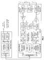
- FIG. 3is a graphical representation of a radio frequency integrated circuit (RFIC) that includes a die 100 , and a package 108 .
- the die 100includes a radio frequency I/O (RFIO) section 102 , a radio frequency to baseband conversion section 104 and a baseband processing section 106 .
- the RFIO section 102includes the low noise amplifier 72 , the receiver filter module 71 , the T/R switch module 73 , the transmit filter module 85 , and the power amplifier 84 .
- the RF to baseband conversion section 104with reference to FIG.
- the baseband processing section 106includes the digital receiver processing module 64 , memory 75 and digital transmitter processing module 76 .
- the package 108includes a plurality of connections 110 , which may include a ball grid array or the package may be an LPCC.
- the die 100is positioned to minimize the trace connection from the RFIO section 102 to the antenna 112 .
- the antenna 112is mounted and/or fabricated on a printed circuit board (PCB) which is coupled via PCB traces 114 to the RE I/O section 102 and, as such, is off-die. Note that the die is off-centered with respect to the package 108 to provide the minimal distance coupling between the RF I/O section 102 and antenna 112 .
- PCBprinted circuit board
- Remaining connections for the baseband processing section 106may include longer traces within package 108 to interconnecting solder balls and/or pins of the package to the PCB without adversely affecting the overall performance of the RFIC. Accordingly, by minimizing the distance between the RE I/O section 102 and the off-die antenna 112 , the corresponding parasitics that are produced by the printed circuit board trace 114 , the coupling of the die 100 to the package 108 , and the coupling of the package 108 to the printed circuit board traces 114 are minimized such that at radio frequencies (e.g., 2.4 gigahertz, 5.25 gigahertz), the parasitics have negligible affect on the performance of the radio frequency integrated circuit.
- radio frequenciese.g., 2.4 gigahertz, 5.25 gigahertz
- FIG. 4is a more detailed graphical representation of coupling the RFIO section 102 of die 100 to off-die antenna 112 .
- the plurality of connections 110includes a ball grid array 120 .
- the solder balls of the ball grid array 120 closest to the off-die antenna 112are used to couple the RF I/O section 102 to the package 108 .
- Corresponding solder balls and/or pins of the packageare then used to couple to PCB traces 114 to provide the connectivity to the off-die antenna 112 . This is further illustrated in FIG. 5 .
- FIG. 5illustrates a side view of the coupling illustrated in FIG. 4 .
- solder ball connections 118couple RF I/O section 102 of die 100 to the package 108 .
- Within the package 108there are traces and/or vias that couple to solder balls and/or pins on the opposite surface of package 108 .
- the other solder ballsare then used to connect to the printed circuit board traces 114 , which couple to the off-die antenna 112 . Accordingly, a minimal distance between the RF I/O section 102 and the off-die antenna 112 may be obtained thereby minimizing the parasitic components and the adverse affects on the performance of the RFIC.
- FIG. 6illustrates an alternate configuration of the RFIC.
- the off-die antenna 112is fabricated on the package 108 .
- the RF I/O section 102 of die 100is connected via package traces and corresponding solder balls to the off-die antenna 112 within the package.
- the distance between the RF I/O section 102 and the off-die antenna 112may be further reduced thereby further reducing the corresponding parasitics and minimizing the adverse affects caused thereby.
- FIG. 7is a logic diagram of a method for multiple packaging of a radio frequency integrated circuit.
- the processbegins at Step 130 where a 1 st position of the RFIC die in a 1 st package (e.g., a ball grid array package) is determined.
- the positionis selected to minimize adverse affects of parasitic components of the coupling between the RFIO section of the die and an antenna as described above.
- Such couplingincludes the coupling of the die to the package and the coupling of the package to the antenna, which may be via traces of a printed circuit board and/or traces within the package.
- the 1 st positionmay be offset from center and may further be at an edge of the 1 st package.
- the parasitic componentsmay include inductance and/or capacitance.
- Step 132the values of the parasitic components are determined.
- Step 134a 2 nd position of the RFIC die within a 2 nd package (e.g., LPCC) is determined based on the values of the parasitic components. The positioning within the 2 nd die is selected such that the values of the parasitic components between the RF I/O section and the antenna substantially match the values of the parasitic components of the coupling between the RFIO section to the antenna in the 1 st package.
- a 2 nd position of the RFIC die within a 2 nd packagee.g., LPCC
- Step 136a determination is made as to whether the die will be packaged in the 1 st package or the 2 nd package.
- the processproceeds to Step 138 where the RFIC die is packaged within the 1 st package in accordance with the 1 st position. If the die is to be packaged in the 2 nd package, the process proceeds to Step 140 where the RFIC die is packaged within the 2 nd package in accordance with the 2 nd position.
- the term “substantially” or “approximately”, as may be used herein,provides an industry-accepted tolerance to its corresponding term. Such an industry-accepted tolerance ranges from less than one percent to twenty percent and corresponds to, but is not limited to, component values, integrated circuit process variations, temperature variations, rise and fall times, and/or thermal noise.
- the term “operably coupled”, as may be used herein,includes direct coupling and indirect coupling via another component, element, circuit, or module where, for indirect coupling, the intervening component, element, circuit, or module does not modify the information of a signal but may adjust its current level, voltage level, and/or power level.
- inferred couplingincludes direct and indirect coupling between two elements in the same manner as “operably coupled”.
- the term “compares favorably”, as may be used herein,indicates that a comparison between two or more elements, items, signals, etc., provides a desired relationship. For example, when the desired relationship is that signal 1 has a greater magnitude than signal 2 , a favorable comparison may be achieved when the magnitude of signal 1 is greater than that of signal 2 or when the magnitude of signal 2 is less than that of signal 1 .
Landscapes
- Engineering & Computer Science (AREA)
- Microelectronics & Electronic Packaging (AREA)
- Physics & Mathematics (AREA)
- Condensed Matter Physics & Semiconductors (AREA)
- General Physics & Mathematics (AREA)
- Computer Hardware Design (AREA)
- Power Engineering (AREA)
- Manufacturing & Machinery (AREA)
- Transceivers (AREA)
Abstract
Description
Claims (5)
Priority Applications (3)
| Application Number | Priority Date | Filing Date | Title |
|---|---|---|---|
| US10/702,402US6998709B2 (en) | 2003-11-05 | 2003-11-05 | RFIC die-package configuration |
| US10/944,526US7264977B2 (en) | 2003-11-05 | 2004-09-17 | Method of RFIC die-package configuration |
| US11/784,878US7329950B2 (en) | 2003-11-05 | 2007-04-10 | RFIC die and package |
Applications Claiming Priority (1)
| Application Number | Priority Date | Filing Date | Title |
|---|---|---|---|
| US10/702,402US6998709B2 (en) | 2003-11-05 | 2003-11-05 | RFIC die-package configuration |
Related Child Applications (1)
| Application Number | Title | Priority Date | Filing Date |
|---|---|---|---|
| US10/944,526DivisionUS7264977B2 (en) | 2003-11-05 | 2004-09-17 | Method of RFIC die-package configuration |
Publications (2)
| Publication Number | Publication Date |
|---|---|
| US20050093132A1 US20050093132A1 (en) | 2005-05-05 |
| US6998709B2true US6998709B2 (en) | 2006-02-14 |
Family
ID=34551668
Family Applications (3)
| Application Number | Title | Priority Date | Filing Date |
|---|---|---|---|
| US10/702,402Expired - LifetimeUS6998709B2 (en) | 2003-11-05 | 2003-11-05 | RFIC die-package configuration |
| US10/944,526Expired - Fee RelatedUS7264977B2 (en) | 2003-11-05 | 2004-09-17 | Method of RFIC die-package configuration |
| US11/784,878Expired - LifetimeUS7329950B2 (en) | 2003-11-05 | 2007-04-10 | RFIC die and package |
Family Applications After (2)
| Application Number | Title | Priority Date | Filing Date |
|---|---|---|---|
| US10/944,526Expired - Fee RelatedUS7264977B2 (en) | 2003-11-05 | 2004-09-17 | Method of RFIC die-package configuration |
| US11/784,878Expired - LifetimeUS7329950B2 (en) | 2003-11-05 | 2007-04-10 | RFIC die and package |
Country Status (1)
| Country | Link |
|---|---|
| US (3) | US6998709B2 (en) |
Cited By (16)
| Publication number | Priority date | Publication date | Assignee | Title |
|---|---|---|---|---|
| US20050070238A1 (en)* | 2003-09-25 | 2005-03-31 | Texas Instruments Incorporated | Method and apparatus for reducing leakage in a direct conversion transmitter |
| US20050151215A1 (en)* | 2004-01-13 | 2005-07-14 | Hauhe Mark S. | Circuit board assembly and method of attaching a chip to a circuit board |
| US20060261950A1 (en)* | 2005-03-29 | 2006-11-23 | Symbol Technologies, Inc. | Smart radio frequency identification (RFID) items |
| US20070278635A1 (en)* | 2006-06-02 | 2007-12-06 | Dingying Xu | Microelectronic package having solder-filled through-vias |
| US20080048307A1 (en)* | 2004-01-28 | 2008-02-28 | Matsushita Electric Industrial Co., Ltd. | Module and Mounted Structure Using the Same |
| US20080265038A1 (en)* | 2004-07-23 | 2008-10-30 | Fractus, S.A. | Antenna in Package with Reduced Electromagnetic Interaction with on Chip Elements |
| US20080315991A1 (en)* | 2007-06-21 | 2008-12-25 | Micron Technology, Inc. | Methods and systems of attaching a radio transceiver to an antenna |
| US20100019038A1 (en)* | 2006-06-23 | 2010-01-28 | Fractus, S.A. | Chip module, sim card, wireless device and wireless communication method |
| WO2010090649A1 (en)* | 2009-02-06 | 2010-08-12 | Rfaxis, Inc. | Radio frequency transceiver front end circuit |
| US20100210223A1 (en)* | 2009-02-17 | 2010-08-19 | Oleksandr Gorbachov | Multi mode radio frequency transceiver front end circuit with inter-stage matching circuit |
| US20100226291A1 (en)* | 2009-03-03 | 2010-09-09 | Oleksandr Gorbachov | Multi-channel radio frequency front end circuit |
| US20100244981A1 (en)* | 2009-03-30 | 2010-09-30 | Oleksandr Gorbachov | Radio frequency power divider and combiner circuit |
| US20100277252A1 (en)* | 2009-05-04 | 2010-11-04 | Oleksandr Gorbachov | Multi-mode radio frequency front end module |
| US20110181488A1 (en)* | 2010-01-25 | 2011-07-28 | Freescale Semiconductor, Inc. | Electronic device module with integrated antenna structure, and related manufacturing method |
| US20140020236A1 (en)* | 2007-01-13 | 2014-01-23 | Panasonic Automotive Systems Company Of America, Division Of Panasonic Corporation Of North America | Highly configurable radio frequency (rf) module |
| US9252767B1 (en)* | 2010-06-28 | 2016-02-02 | Hittite Microwave Corporation | Integrated switch module |
Families Citing this family (15)
| Publication number | Priority date | Publication date | Assignee | Title |
|---|---|---|---|---|
| US7257093B1 (en)* | 2001-10-10 | 2007-08-14 | Sandia Corporation | Localized radio frequency communication using asynchronous transfer mode protocol |
| US8768411B2 (en)* | 2005-09-30 | 2014-07-01 | Intel Corporation | Systems and methods for RF communication between processors |
| US20080246139A1 (en)* | 2007-04-03 | 2008-10-09 | Don Craven | Polar hybrid grid array package |
| EP2269220A1 (en)* | 2008-03-22 | 2011-01-05 | Nxp B.V. | Esd networks for solder bump integrated circuits |
| GB0815306D0 (en)* | 2008-08-21 | 2008-09-24 | Sarantel Ltd | An antenna and a method of manufacturing an antenna |
| US8269671B2 (en)* | 2009-01-27 | 2012-09-18 | International Business Machines Corporation | Simple radio frequency integrated circuit (RFIC) packages with integrated antennas |
| US8256685B2 (en)* | 2009-06-30 | 2012-09-04 | International Business Machines Corporation | Compact millimeter wave packages with integrated antennas |
| JP5480299B2 (en) | 2010-01-05 | 2014-04-23 | 株式会社東芝 | Antenna and radio apparatus |
| JP5172925B2 (en) | 2010-09-24 | 2013-03-27 | 株式会社東芝 | Wireless device |
| JP5417389B2 (en) | 2011-07-13 | 2014-02-12 | 株式会社東芝 | Wireless device |
| JP5414749B2 (en) | 2011-07-13 | 2014-02-12 | 株式会社東芝 | Wireless device |
| JP6121705B2 (en) | 2012-12-12 | 2017-04-26 | 株式会社東芝 | Wireless device |
| US9350392B2 (en)* | 2012-12-12 | 2016-05-24 | Qualcomm Incorporated | RFIC configuration for reduced antenna trace loss |
| US9900102B2 (en)* | 2015-12-01 | 2018-02-20 | Intel Corporation | Integrated circuit with chip-on-chip and chip-on-substrate configuration |
| CN109712943B (en)* | 2017-10-26 | 2020-11-20 | 联发科技股份有限公司 | Semiconductor Package Components |
Citations (7)
| Publication number | Priority date | Publication date | Assignee | Title |
|---|---|---|---|---|
| US5371404A (en)* | 1993-02-04 | 1994-12-06 | Motorola, Inc. | Thermally conductive integrated circuit package with radio frequency shielding |
| WO1999067754A1 (en)* | 1998-06-23 | 1999-12-29 | Motorola Inc. | Radio frequency identification tag having a printed antenna and method |
| EP1126522A1 (en)* | 2000-02-18 | 2001-08-22 | Alcatel | Packaged integrated circuit with radio frequency antenna |
| US6580163B2 (en)* | 2001-06-18 | 2003-06-17 | Research In Motion Limited | IC chip packaging for reducing bond wire length |
| US20040164382A1 (en)* | 2003-02-21 | 2004-08-26 | Gerber Mark A. | Multi-die semiconductor package |
| US6787901B2 (en)* | 2001-08-17 | 2004-09-07 | Qualcomm Incorporated | Stacked dies utilizing cross connection bonding wire |
| US6807063B2 (en)* | 2002-03-14 | 2004-10-19 | Fujitsu Limited | High-frequency integrated circuit module |
Family Cites Families (6)
| Publication number | Priority date | Publication date | Assignee | Title |
|---|---|---|---|---|
| JP3141692B2 (en)* | 1994-08-11 | 2001-03-05 | 松下電器産業株式会社 | Millimeter wave detector |
| JP3472430B2 (en)* | 1997-03-21 | 2003-12-02 | シャープ株式会社 | Antenna integrated high frequency circuit |
| US6242163B1 (en)* | 1998-08-31 | 2001-06-05 | Board Of Trustees Of The Leland Stanford Junior University | Shape deposition manufacturing of microscopic ceramic and metallic parts using silicon molds |
| JP2001244127A (en)* | 2000-02-29 | 2001-09-07 | Murata Mfg Co Ltd | High-frequency component and communication apparatus |
| TW523920B (en)* | 2000-11-18 | 2003-03-11 | Lenghways Technology Co Ltd | Integrated multi-channel communication passive device manufactured by using micro-electromechanical technique |
| US6734539B2 (en)* | 2000-12-27 | 2004-05-11 | Lucent Technologies Inc. | Stacked module package |
- 2003
- 2003-11-05USUS10/702,402patent/US6998709B2/ennot_activeExpired - Lifetime
- 2004
- 2004-09-17USUS10/944,526patent/US7264977B2/ennot_activeExpired - Fee Related
- 2007
- 2007-04-10USUS11/784,878patent/US7329950B2/ennot_activeExpired - Lifetime
Patent Citations (7)
| Publication number | Priority date | Publication date | Assignee | Title |
|---|---|---|---|---|
| US5371404A (en)* | 1993-02-04 | 1994-12-06 | Motorola, Inc. | Thermally conductive integrated circuit package with radio frequency shielding |
| WO1999067754A1 (en)* | 1998-06-23 | 1999-12-29 | Motorola Inc. | Radio frequency identification tag having a printed antenna and method |
| EP1126522A1 (en)* | 2000-02-18 | 2001-08-22 | Alcatel | Packaged integrated circuit with radio frequency antenna |
| US6580163B2 (en)* | 2001-06-18 | 2003-06-17 | Research In Motion Limited | IC chip packaging for reducing bond wire length |
| US6787901B2 (en)* | 2001-08-17 | 2004-09-07 | Qualcomm Incorporated | Stacked dies utilizing cross connection bonding wire |
| US6807063B2 (en)* | 2002-03-14 | 2004-10-19 | Fujitsu Limited | High-frequency integrated circuit module |
| US20040164382A1 (en)* | 2003-02-21 | 2004-08-26 | Gerber Mark A. | Multi-die semiconductor package |
Cited By (51)
| Publication number | Priority date | Publication date | Assignee | Title |
|---|---|---|---|---|
| US7509101B2 (en)* | 2003-09-25 | 2009-03-24 | Texas Instruments Incorporated | Method and apparatus for reducing leakage in a direct conversion transmitter |
| US20050070238A1 (en)* | 2003-09-25 | 2005-03-31 | Texas Instruments Incorporated | Method and apparatus for reducing leakage in a direct conversion transmitter |
| US20050151215A1 (en)* | 2004-01-13 | 2005-07-14 | Hauhe Mark S. | Circuit board assembly and method of attaching a chip to a circuit board |
| US7298235B2 (en)* | 2004-01-13 | 2007-11-20 | Raytheon Company | Circuit board assembly and method of attaching a chip to a circuit board with a fillet bond not covering RF traces |
| US7667974B2 (en)* | 2004-01-28 | 2010-02-23 | Panasonic Corporation | Module and mounted structure using the same |
| US7859855B2 (en) | 2004-01-28 | 2010-12-28 | Panasonic Corporation | Module and mounted structure using the same |
| US20080048307A1 (en)* | 2004-01-28 | 2008-02-28 | Matsushita Electric Industrial Co., Ltd. | Module and Mounted Structure Using the Same |
| US20100133664A1 (en)* | 2004-01-28 | 2010-06-03 | Panasonic Corporation | Module and mounted structure using the same |
| US20080265038A1 (en)* | 2004-07-23 | 2008-10-30 | Fractus, S.A. | Antenna in Package with Reduced Electromagnetic Interaction with on Chip Elements |
| US8330259B2 (en)* | 2004-07-23 | 2012-12-11 | Fractus, S.A. | Antenna in package with reduced electromagnetic interaction with on chip elements |
| US20060261950A1 (en)* | 2005-03-29 | 2006-11-23 | Symbol Technologies, Inc. | Smart radio frequency identification (RFID) items |
| US7638867B2 (en) | 2006-06-02 | 2009-12-29 | Intel Corporation | Microelectronic package having solder-filled through-vias |
| US20070278635A1 (en)* | 2006-06-02 | 2007-12-06 | Dingying Xu | Microelectronic package having solder-filled through-vias |
| US20100019038A1 (en)* | 2006-06-23 | 2010-01-28 | Fractus, S.A. | Chip module, sim card, wireless device and wireless communication method |
| US8196829B2 (en) | 2006-06-23 | 2012-06-12 | Fractus, S.A. | Chip module, sim card, wireless device and wireless communication method |
| US9225366B2 (en)* | 2007-01-13 | 2015-12-29 | Panasonic Automotive Systems Company Of America, Division Of Panasonic Corporation Of North America | Method of manufacturing a radio frequency receiver module |
| US20140020236A1 (en)* | 2007-01-13 | 2014-01-23 | Panasonic Automotive Systems Company Of America, Division Of Panasonic Corporation Of North America | Highly configurable radio frequency (rf) module |
| US8432284B2 (en) | 2007-06-21 | 2013-04-30 | Round Rock Research, Llc | Methods and systems of attaching a radio transceiver to an antenna |
| US7696885B2 (en)* | 2007-06-21 | 2010-04-13 | Round Rock Research, Llc | Methods and systems of attaching a radio transceiver to an antenna |
| US20080315991A1 (en)* | 2007-06-21 | 2008-12-25 | Micron Technology, Inc. | Methods and systems of attaching a radio transceiver to an antenna |
| US8140025B2 (en) | 2009-02-06 | 2012-03-20 | Rfaxis, Inc. | Single input/output port radio frequency transceiver front end circuit with low noise amplifier switching transistor |
| US20100203844A1 (en)* | 2009-02-06 | 2010-08-12 | Oleksandr Gorbachov | Radio frequency transceiver front end circuit |
| WO2010090649A1 (en)* | 2009-02-06 | 2010-08-12 | Rfaxis, Inc. | Radio frequency transceiver front end circuit |
| CN102356556B (en)* | 2009-02-06 | 2014-11-12 | Rfaxis股份有限公司 | RF Transceiver Front-End Circuit |
| US20100203843A1 (en)* | 2009-02-06 | 2010-08-12 | Oleksandr Gorbachov | Radio frequency transceiver front end circuit with direct current bias switch |
| US20100203846A1 (en)* | 2009-02-06 | 2010-08-12 | Oleksandr Gorbachov | Radio frequency transceiver front end circuit with parallel resonant circuit |
| US8301084B2 (en) | 2009-02-06 | 2012-10-30 | Rfaxis, Inc. | Radio frequency transceiver front end circuit with direct current bias switch |
| US8265567B2 (en) | 2009-02-06 | 2012-09-11 | Rfaxis Inc. | Single input/output port radio frequency transceiver front end circuit |
| US20100203847A1 (en)* | 2009-02-06 | 2010-08-12 | Oleksandr Gorbachov | Single input/output port radio frequency transceiver front end circuit |
| US20100202324A1 (en)* | 2009-02-06 | 2010-08-12 | Oleksandr Gorbachov | Radio frequency transceiver front end circuit with matching circuit voltage divider |
| US8175541B2 (en) | 2009-02-06 | 2012-05-08 | Rfaxis, Inc. | Radio frequency transceiver front end circuit |
| US8019289B2 (en) | 2009-02-06 | 2011-09-13 | Rfaxis, Inc. | Radio frequency transceiver front end circuit with matching circuit voltage divider |
| US20100203845A1 (en)* | 2009-02-06 | 2010-08-12 | Oleksandr Gorbachov | Single input/output port radio frequency transceiver front end circuit with low noise amplifier switching transistor |
| US8135355B2 (en) | 2009-02-06 | 2012-03-13 | Rfaxis, Inc. | Radio frequency transceiver front end circuit with parallel resonant circuit |
| US20100210223A1 (en)* | 2009-02-17 | 2010-08-19 | Oleksandr Gorbachov | Multi mode radio frequency transceiver front end circuit with inter-stage matching circuit |
| US8073400B2 (en) | 2009-02-17 | 2011-12-06 | Rfaxis, Inc. | Multi mode radio frequency transceiver front end circuit |
| US8073401B2 (en) | 2009-02-17 | 2011-12-06 | Rfaxis, Inc. | Multi mode radio frequency transceiver front end circuit with inter-stage matching circuit |
| US20100210299A1 (en)* | 2009-02-17 | 2010-08-19 | Oleksandr Gorbachov | Multi mode radio frequency transceiver front end circuit |
| US20100210208A1 (en)* | 2009-02-17 | 2010-08-19 | Oleksandr Gorbachov | Multi mode radio frequency transceiver front end circuit with inter-stage power divider |
| US8078119B2 (en) | 2009-02-17 | 2011-12-13 | Rfaxis, Inc. | Multi mode radio frequency transceiver front end circuit with inter-stage power divider |
| US20100226291A1 (en)* | 2009-03-03 | 2010-09-09 | Oleksandr Gorbachov | Multi-channel radio frequency front end circuit |
| US8325632B2 (en) | 2009-03-03 | 2012-12-04 | Rfaxis, Inc. | Multi-channel radio frequency front end circuit with full receive diversity for multi-path mitigation |
| US20100226292A1 (en)* | 2009-03-03 | 2010-09-09 | Oleksandr Gorbachov | Multi-channel radio frequency front end circuit with full receive diversity for multi-path mitigation |
| US20100225414A1 (en)* | 2009-03-03 | 2010-09-09 | Oleksandr Gorbachov | Multi-channel radio frequency front end circuit with full transmit and receive diversity for multi-path mitigation |
| US9231680B2 (en) | 2009-03-03 | 2016-01-05 | Rfaxis, Inc. | Multi-channel radio frequency front end circuit |
| US20100244981A1 (en)* | 2009-03-30 | 2010-09-30 | Oleksandr Gorbachov | Radio frequency power divider and combiner circuit |
| US8467738B2 (en) | 2009-05-04 | 2013-06-18 | Rfaxis, Inc. | Multi-mode radio frequency front end module |
| US20100277252A1 (en)* | 2009-05-04 | 2010-11-04 | Oleksandr Gorbachov | Multi-mode radio frequency front end module |
| US8407890B2 (en)* | 2010-01-25 | 2013-04-02 | Freescale Semiconductor Inc. | Method of manufacting an electronic device module with integrated antenna structure |
| US20110181488A1 (en)* | 2010-01-25 | 2011-07-28 | Freescale Semiconductor, Inc. | Electronic device module with integrated antenna structure, and related manufacturing method |
| US9252767B1 (en)* | 2010-06-28 | 2016-02-02 | Hittite Microwave Corporation | Integrated switch module |
Also Published As
| Publication number | Publication date |
|---|---|
| US20070187809A1 (en) | 2007-08-16 |
| US7329950B2 (en) | 2008-02-12 |
| US7264977B2 (en) | 2007-09-04 |
| US20050093132A1 (en) | 2005-05-05 |
| US20050095747A1 (en) | 2005-05-05 |
Similar Documents
| Publication | Publication Date | Title |
|---|---|---|
| US7329950B2 (en) | RFIC die and package | |
| US7551901B2 (en) | Linear high powered integrated circuit amplifier | |
| US7583212B2 (en) | Reduced noise radio frequency integrated circuit | |
| US7822394B2 (en) | Electrostatic protection circuit with impedance matching for radio frequency integrated circuits | |
| US7373116B2 (en) | High output power radio frequency integrated circuit | |
| US8208863B2 (en) | Radio frequency unit analog level detector and feedback control system | |
| US7079816B2 (en) | On chip diversity antenna switch | |
| US20070032064A1 (en) | Use of an internal on-chip inductor for electrostatic discharge protection of circuits which use bond wire inductance as their load | |
| US8768284B2 (en) | Radio frequency integrated circuit with noise immunity border | |
| US7215932B2 (en) | On-chip impedance matching power amplifier | |
| US7187061B2 (en) | Use of a down-bond as a controlled inductor in integrated circuit applications | |
| US7391596B2 (en) | High frequency integrated circuit pad configuration including ESD protection circuitry | |
| US7522394B2 (en) | Radio frequency integrated circuit having sectional ESD protection | |
| US20040063412A1 (en) | Attenuation of a received radio frequency signal | |
| US7415246B2 (en) | Attenuation of high-power inbound RF signals based on attenuation of a T/R switch | |
| US20060066431A1 (en) | Adjustable differential inductor | |
| US7457380B2 (en) | Low noise circuit and applications thereof |
Legal Events
| Date | Code | Title | Description |
|---|---|---|---|
| AS | Assignment | Owner name:BROADCOM CORPORATION, CALIFORNIA Free format text:ASSIGNMENT OF ASSIGNORS INTEREST;ASSIGNOR:KHORRAM, SHAHLA;REEL/FRAME:014685/0547 Effective date:20031014 | |
| STCF | Information on status: patent grant | Free format text:PATENTED CASE | |
| FPAY | Fee payment | Year of fee payment:4 | |
| FPAY | Fee payment | Year of fee payment:8 | |
| AS | Assignment | Owner name:BANK OF AMERICA, N.A., AS COLLATERAL AGENT, NORTH CAROLINA Free format text:PATENT SECURITY AGREEMENT;ASSIGNOR:BROADCOM CORPORATION;REEL/FRAME:037806/0001 Effective date:20160201 Owner name:BANK OF AMERICA, N.A., AS COLLATERAL AGENT, NORTH Free format text:PATENT SECURITY AGREEMENT;ASSIGNOR:BROADCOM CORPORATION;REEL/FRAME:037806/0001 Effective date:20160201 | |
| AS | Assignment | Owner name:AVAGO TECHNOLOGIES GENERAL IP (SINGAPORE) PTE. LTD., SINGAPORE Free format text:ASSIGNMENT OF ASSIGNORS INTEREST;ASSIGNOR:BROADCOM CORPORATION;REEL/FRAME:041706/0001 Effective date:20170120 Owner name:AVAGO TECHNOLOGIES GENERAL IP (SINGAPORE) PTE. LTD Free format text:ASSIGNMENT OF ASSIGNORS INTEREST;ASSIGNOR:BROADCOM CORPORATION;REEL/FRAME:041706/0001 Effective date:20170120 | |
| AS | Assignment | Owner name:BROADCOM CORPORATION, CALIFORNIA Free format text:TERMINATION AND RELEASE OF SECURITY INTEREST IN PATENTS;ASSIGNOR:BANK OF AMERICA, N.A., AS COLLATERAL AGENT;REEL/FRAME:041712/0001 Effective date:20170119 | |
| FPAY | Fee payment | Year of fee payment:12 | |
| AS | Assignment | Owner name:AVAGO TECHNOLOGIES INTERNATIONAL SALES PTE. LIMITE Free format text:MERGER;ASSIGNOR:AVAGO TECHNOLOGIES GENERAL IP (SINGAPORE) PTE. LTD.;REEL/FRAME:047196/0097 Effective date:20180509 | |
| AS | Assignment | Owner name:AVAGO TECHNOLOGIES INTERNATIONAL SALES PTE. LIMITE Free format text:CORRECTIVE ASSIGNMENT TO CORRECT THE EXECUTION DATE PREVIOUSLY RECORDED AT REEL: 047196 FRAME: 0097. ASSIGNOR(S) HEREBY CONFIRMS THE MERGER;ASSIGNOR:AVAGO TECHNOLOGIES GENERAL IP (SINGAPORE) PTE. LTD.;REEL/FRAME:048555/0510 Effective date:20180905 |