US6995890B2 - Interference display unit - Google Patents
Interference display unitDownload PDFInfo
- Publication number
- US6995890B2 US6995890B2US10/706,923US70692303AUS6995890B2US 6995890 B2US6995890 B2US 6995890B2US 70692303 AUS70692303 AUS 70692303AUS 6995890 B2US6995890 B2US 6995890B2
- Authority
- US
- United States
- Prior art keywords
- display unit
- optical interference
- electrode
- interference display
- electrodes
- Prior art date
- Legal status (The legal status is an assumption and is not a legal conclusion. Google has not performed a legal analysis and makes no representation as to the accuracy of the status listed.)
- Expired - Fee Related, expires
Links
Images


Classifications
- G—PHYSICS
- G02—OPTICS
- G02F—OPTICAL DEVICES OR ARRANGEMENTS FOR THE CONTROL OF LIGHT BY MODIFICATION OF THE OPTICAL PROPERTIES OF THE MEDIA OF THE ELEMENTS INVOLVED THEREIN; NON-LINEAR OPTICS; FREQUENCY-CHANGING OF LIGHT; OPTICAL LOGIC ELEMENTS; OPTICAL ANALOGUE/DIGITAL CONVERTERS
- G02F1/00—Devices or arrangements for the control of the intensity, colour, phase, polarisation or direction of light arriving from an independent light source, e.g. switching, gating or modulating; Non-linear optics
- G02F1/01—Devices or arrangements for the control of the intensity, colour, phase, polarisation or direction of light arriving from an independent light source, e.g. switching, gating or modulating; Non-linear optics for the control of the intensity, phase, polarisation or colour
- G02F1/13—Devices or arrangements for the control of the intensity, colour, phase, polarisation or direction of light arriving from an independent light source, e.g. switching, gating or modulating; Non-linear optics for the control of the intensity, phase, polarisation or colour based on liquid crystals, e.g. single liquid crystal display cells
- G02F1/133—Constructional arrangements; Operation of liquid crystal cells; Circuit arrangements
- G02F1/1333—Constructional arrangements; Manufacturing methods
- G02F1/1343—Electrodes
- G—PHYSICS
- G02—OPTICS
- G02B—OPTICAL ELEMENTS, SYSTEMS OR APPARATUS
- G02B26/00—Optical devices or arrangements for the control of light using movable or deformable optical elements
- G02B26/001—Optical devices or arrangements for the control of light using movable or deformable optical elements based on interference in an adjustable optical cavity
- B—PERFORMING OPERATIONS; TRANSPORTING
- B81—MICROSTRUCTURAL TECHNOLOGY
- B81C—PROCESSES OR APPARATUS SPECIALLY ADAPTED FOR THE MANUFACTURE OR TREATMENT OF MICROSTRUCTURAL DEVICES OR SYSTEMS
- B81C1/00—Manufacture or treatment of devices or systems in or on a substrate
- B81C1/00015—Manufacture or treatment of devices or systems in or on a substrate for manufacturing microsystems
- B81C1/00134—Manufacture or treatment of devices or systems in or on a substrate for manufacturing microsystems comprising flexible or deformable structures
- B81C1/00182—Arrangements of deformable or non-deformable structures, e.g. membrane and cavity for use in a transducer
- G—PHYSICS
- G02—OPTICS
- G02B—OPTICAL ELEMENTS, SYSTEMS OR APPARATUS
- G02B5/00—Optical elements other than lenses
- G02B5/20—Filters
- G02B5/201—Filters in the form of arrays
- G—PHYSICS
- G02—OPTICS
- G02B—OPTICAL ELEMENTS, SYSTEMS OR APPARATUS
- G02B5/00—Optical elements other than lenses
- G02B5/20—Filters
- G02B5/28—Interference filters
- G02B5/284—Interference filters of etalon type comprising a resonant cavity other than a thin solid film, e.g. gas, air, solid plates
- B—PERFORMING OPERATIONS; TRANSPORTING
- B81—MICROSTRUCTURAL TECHNOLOGY
- B81B—MICROSTRUCTURAL DEVICES OR SYSTEMS, e.g. MICROMECHANICAL DEVICES
- B81B2201/00—Specific applications of microelectromechanical systems
- B81B2201/04—Optical MEMS
- B81B2201/047—Optical MEMS not provided for in B81B2201/042 - B81B2201/045
Definitions
- the present inventionrelates to a method for manufacturing an optical interference display. More particularly, the present invention relates to a method for manufacturing an optical interference display with posts of arms.
- Planar displaysare popular for portable displays and displays with space limits because they are light and small in size. To date, planar displays in addition to liquid crystal displays (LCD), organic electro-luminescent displays (OLED), plasma display panels (PDP) and so on, as well as a mode of the optical interference display are of interest.
- LCDliquid crystal displays
- OLEDorganic electro-luminescent displays
- PDPplasma display panels
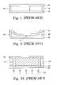
- U.S. Pat. No. 5,835,255discloses an array of display units of visible light that can be used in a planar display. Please refer to FIG. 1 , which depicts a cross-sectional view of a display unit in the prior art.
- Every optical interference display unit 100comprises two walls, 102 and 104 .
- Posts 106support these two walls 102 and 104 , and a cavity 108 is subsequently formed.
- the distance between these two walls 102 and 104that is, the length of the cavity 108 , is D.
- One of the walls 102 and 104is a hemi-transmissible/hemi-reflective layer with an absorption rate that partially absorbs visible light, and the other is a light reflective layer that is deformable when voltage is applied.
- Nis a natural number
- the display unit 100is “open”.
- the first wall 102is a hemi-transmissible/hemi-reflective electrode that comprises a substrate, an absorption layer, and a dielectric layer. Incident light passing through the first wall 102 is partially absorbed by the absorption layer.
- the substrateis made from conductive and transparent materials, such as ITO glass or IZO glass.
- the absorption layeris made from metal, such as aluminum, chromium or silver and so on.
- the dielectric layeris made from silicon oxide, silicon nitrite or metal oxide. Metal oxide can be obtained by directly oxidizing a portion of the absorption layer.
- the second wall 104is a deformable reflective electrode. It shifts up and down by applying a voltage.
- the second wall 104is typically made from dielectric materials/conductive transparent materials, or metal/conductive transparent materials.
- FIG. 2depicts a cross-sectional view of a display unit in the prior art after applying a voltage.
- the wall 104is deformed and falls down towards the wall 102 due to the attraction of static electricity.
- the distance between wall 102 and 104that is, the length of the cavity 108 is not exactly zero, but is d, which can be zero. If we use d instead of D in formula 1.1, only the visible light with a wavelength satisfying formula 1.1, which is ⁇ 2 , can generate a constructive interference, and be reflected by the wall 104 , and pass through the wall 102 .
- wall 102has a high light absorption rate for light with wavelength ⁇ 2 , all the incident light in the visible light spectrum is filtered out and an observer who follows the direction of the incident light cannot observe any reflected light in the visible light spectrum.
- the display unit 100is now “closed”.
- FIG. 1shows that the posts 106 of the display unit 100 are generally made from negative photoresist materials.
- FIGS. 3A to 3Cdepict a method for manufacturing a display unit in the prior art.
- the first wall 102 and a sacrificial layer 110are formed in order on a transparent substrate 109 , and then an opening 112 is formed in the wall 102 and the sacrificial layer 110 .
- the opening 112is suitable for forming posts therein.
- a negative photoresist layer 111is spin-coated on the sacrificial layer 110 and fills the opening 112 .
- the objective of forming the negative photoresist layer 111is to form posts between the first wall 102 and the second wall (not shown).
- a backside exposure processis performed on the negative photoresist layer 111 in the opening 112 , in the direction indicated by arrow 113 to the transparent substrate 109 .
- the sacrificial layer 110must be made from opaque materials, typically metal materials, to meet the needs of the backside exposure process.
- FIG. 3Bwhich shows that posts 106 remain in the opening 112 after removing the unexposed negative photoresist layer.
- the wall 104is formed on the sacrificial layer 110 and posts 106 .
- the sacrificial layer 110is removed by a release etching process to form a cavity 114 .
- the length D of the cavity 114is the thickness of the sacrificial layer 110 . Therefore, different thicknesses of the sacrificial layers must be used in different processes of the different display units to control reflection of light with different wavelengths.
- An array comprising the display unit 100 controlled by voltage operationis sufficient for a single color planar display, but not for a color planar display.
- a method in the prior artis to manufacture a pixel that comprises three display units with different cavity lengths as shown in FIG. 4 , which depicts a cross-sectional view of a matrix color planar display in the prior art.
- Three display units 302 , 304 and 306are formed as an array on a substrate 300 , respectively.
- Display units 302 , 304 and 306can reflect an incident light 308 to color lights with different wavelengths, for example, which are red, green and blue lights, due to the different lengths of the cavities of the display units 302 , 304 and 306 . It is not required that different reflective mirrors be used for the display units arranged in the array. More important is that good resolution be provided and the brightness of all color lights is uniform. However, three display units with different lengths of cavities need to be manufactured separately.
- FIGS. 5A to 5Ddepict cross-sectional views of a method for manufacturing the matrix color planar display in the prior art.
- the first wall 310 and the first sacrificial layer 312are formed in order on a transparent substrate 300 , and then openings 314 , 316 , 318 , and 320 are formed in the first wall 310 and the sacrificial layer 312 for defining predetermined positions where display units 302 , 304 , and 306 are formed.
- the second sacrificial layer 322is then conformally formed on the first sacrificial layer 312 and in the openings 314 , 316 , 318 , and 320 .
- the third sacrificial layer 324is conformally formed on the first sacrificial layer 312 and the second sacrificial layer 322 and in the openings 314 , 316 , 318 and 320 .
- FIG. 5Cshows that the third sacrificial layer 324 in the openings 318 and 320 remains but the remainder of the third sacrificial layer 324 is removed by a photolithographic etch process.
- a negative photoresistis spin-coated on the first sacrificial layer 312 , the second sacrificial layer 322 , and the third sacrificial layer 324 , and in the openings 314 , 316 , 318 and 320 , and fills the all openings to form a negative photoresist layer 326 .
- the negative photoresist layer 326is used for forming posts (not shown) between the first wall 310 and the second wall (not shown).
- FIG. 5Dshows that a backside exposure process is performed on the negative photoresist layer 326 in the openings 314 , 316 , 318 and 320 in a direction of the transparent substrate 300 .
- the sacrificial layer 110must be made at least from opaque materials, typically metal materials, to meet the needs of the backside exposure process.
- Posts 328remain in the openings 314 , 316 , 318 and 320 after removing the unexposed negative photoresist layer 326 .
- the second wall 330conformally covers the first sacrificial layer 312 , the second sacrificial layer 322 , the third sacrificial layer 324 and posts 328 .
- the first sacrificial layer 312 , the second sacrificial layer 322 , and the third sacrificial layer 324are removed by a release etching process to form the display units 302 , 304 , and 306 shown in FIG. 4 , wherein the lengths d1, d2, and d3 of three display units 302 , 304 , and 306 are the thicknesses of the first sacrificial layer 312 , the second sacrificial layer 322 , and the third sacrificial layer 324 , respectively. Therefore, different thicknesses of sacrificial layers must be used in different processes of the different display units, to achieve the objective for controlling reflection of different wavelengths of light.
- one preferred embodiment of the inventionprovides a method for manufacturing an optical interference display unit structure.
- the optical interference display unit structurehas a first electrode and a second electrode. Posts are located between the two electrodes and support the electrodes.
- the feature of the present inventionis that the thickness of the second electrode is convertible. Therefore, the stress of the second electrode with different thickness is different. After a thermal process, the second electrode may generate displacement by stress action. The distance between two electrodes may alters because the different displacement of the second electrode.
- the method of fabricating the optical interference display unit structureis also disclosed in the same embodiment.
- the first wall and a sacrificial layerare formed in order on a transparent substrate, and then openings are formed in the first wall and the sacrificial layer.
- the openingsare suitable for forming posts therein.
- a photoresist layeris spin-coated on the sacrificial layer and fills the opening.
- a photolithographic processpatterns the photoresist layer to define a post.
- the postcould comprise a support and an arm, the support is formed in one opening and the arm is formed on the top of the support and on the sacrificial layer.
- the support and the armare used for a post.
- One or multi conductive layerare formed on the sacrificial layer and posts, and the conductive layer(s) is/are used as the second wall.
- the dielectric layeralso can be used to alter the thickness or the stress of the second wall.
- a thermal processsuch as a backing process is performed on the structures.
- the second wallmay generate different displacement by stress action because the different stress of the second wall and the distance between two walls is different. If the post has an arm, the total stress of the arm and the second wall decides the distance between the two walls.
- the sacrificial layeris removed by a release etching process to form a cavity, and the length D of the cavity may not be equal to the thickness of the sacrificial layer due to the displacement of the second wall.
- the arms of the post with the ratios of various length to thicknesshave various amounts of stress, and displacements and directions generated by arms are various during baking. Therefore, the arms with the ratios of various lengths to thickness and the thickness of the second wall may be used for controlling the length of the cavity, instead of the various thickness of the sacrificial layers used in the various processes of the display units to control various wavelengths of light reflected in the prior art.
- the costdrops drastically.
- the thickness of the cavity in the prior artis the thickness of the sacrificial layer, and the sacrificial layer needs to be removed at the end of the process.
- the present inventionutilizes a mask for a front exposure, so the sacrificial layer can be transparent materials such as dielectric materials, instead of opaque materials such as metal and the like as in the prior art. Besides, the thickness used by the sacrificial layer can be substantially reduced, so the time required for the release etching process can be also drastically decreased. Third, the color optical interference display formed by using posts can substantially reduce complexity of the process. The difference in the ratios of thickness of the second wall is used for changing the stress of the second wall. After baking, various optical interference display units have various lengths of the cavities due to the displacement of the second wall, such that reflected light is changed with various wavelengths, such as red, green, and blue lights, so as to obtain various color lights.
- one preferred embodiment of the inventionprovides a method for manufacturing a matrix color planar display structure.
- Each matrix color planar display unithas three optical interference display units.
- the first wall and a sacrificial layerare formed in order on a transparent substrate, and then an opening is formed in the first wall and the sacrificial layer.
- the openingis suitable for forming posts therein.
- a photoresist layeris spin-coated on the sacrificial layer and fills the opening.
- a photolithographic processpatterns the photoresist layer to define a support with an arm.
- the support and the armare used for a post, and to define the length of the arm.
- a first electrode layeris formed on the three optical interference display unit and a second electrode layer is formed on the first electrode layer which is on the second and the third optical interference display units.
- a third electrode layeris formed on the second electrode layer which is on the third optical interference display unit.
- the first electrode layeris the second wall of the first optical interference display unit, the first electrode layer and the second electrode layer are the second wall of the second optical interference display unit, and the first electrode layer, the second electrode layer and the third electrode layer are the second wall of the third optical interference display unit. Therefore, the thickness of the second wall of the three optical interference display unit is different and the stress of the second wall on the three optical interference display unit is different, too.
- the sacrificial layerdue to the exposure of the photoresist layer with the help of a mask, the sacrificial layer no longer must be an opaque material such as metal and the like; common dielectric materials are also used for making the sacrificial layer.
- the second wallis formed on the sacrificial layer and posts, and then baking is performed on the posts.
- the second wallmay generate displacement by stress action.
- the displacements of the second walls of the different optical interference display unitare different because the thickness of the second wall of the different optical interference display unit is different.
- the sacrificial layerare removed by a release etching process to form a cavity, and the length D of the cavity may not be equal to the thickness of the sacrificial layer due to the displacement of the arm.
- the first wallis the first electrode
- the second wallis the second electrode.
- the thickness of the second wall of the different optical interference display unitis different, however, the stress of the second wall of the different optical interference display unit is also different. Therefore, the displacement of the second electrodes is different after a baking process.
- the distance between the two electrodes, i.e. the length of the cavity, of the different optical interference display unitis different. Therefore, after baking, each optical interference display unit has various cavity lengths, such that reflected light is changed with different wavelengths, such as red, green, and blue light. These in turn provide various color lights for a matrix color planar display structure.
- the advantages of a matrix color planar display according to the prior artare retained, including high resolution and high brightness, as well as the advantages of a multi-layered color planar display with a simple process and high yield in the prior art. It is understood that the present invention discloses an optical interference display unit which not only keeps all advantages of the prior optical interference color planar display such as high resolution, high brightness, simple process and high yield during forming arrays, but also increases the window during processing and raises the yield of the optical interference color planar display.
- FIG. 1depicts a cross-sectional view of a display unit in the prior art
- FIG. 2depicts a cross-sectional view of a display unit in the prior art after applying a voltage
- FIGS. 3A to 3Cdepict a method for manufacturing a display unit in the prior art
- FIG. 4depicts a cross-sectional view of a matrix color planar display in the prior art
- FIGS. 5A to 5Ddepict cross-sectional views of a method of manufacturing a matrix color planar display in the prior art.
- FIGS. 6A to 6Edepict a method for manufacturing an optical interference display unit according to one preferred embodiment of this invention.
- the first embodimentis provided herein to explain the optical interference display unit structure in this invention.
- the second embodimentis provided to give further description of the optical interference color planar display formed with an array of the optical interference display unit.
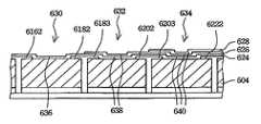
- FIGS. 6A to 6Edepict a method for manufacturing an optical interference display unit according to a preferred embodiment of the invention.
- a first electrode 602 and a sacrificial layer 604are formed in order on a transparent substrate 601 .
- the sacrificial layer 604is made of transparent materials such as dielectric materials, or opaque materials such as metal materials.
- Opening 606 , 608 , 610 and 612are formed in the first electrode 602 and the sacrificial layer 604 by a photolithographic etching process.
- the openings 606 , 608 , 610 and 612are suitable for forming a post therein.
- a material layer 614is formed on the sacrificial layer 604 and fills the openings 606 , 608 , 610 and 612 . Openings 606 and 608 , openings 608 and 610 , and openings 610 and 612 are used to define the location of the optical interference display units 630 , 632 and 634 .
- the material layer 614is suitable for forming posts, and the material layer 614 generally uses photosensitive materials such as photoresists, or non-photosensitive polymer materials such as polyester, polyamide or the like. If non-photosensitive materials are used for forming the material layer 614 , a photolithographic etch process is required to define posts in the material layer 614 . In this embodiment, the photosensitive materials are used for forming the material layer 614 , so merely a photolithographic etching process is required for patterning the material layer 614 .
- the posts 616 , 618 , 620 and 622are defined by patterning the material layer 614 during a photolithographic process.
- the posts 616 , 618 , 620 and 622have supports 6161 , 6181 , 6201 and 6221 disposed in the openings 606 , 608 , 610 and 612 , and the posts 616 , 618 , 620 and 622 have arms 6162 , 6182 , 6183 , 6202 , 6203 and 6222 .
- the length of arms 6162 , 6182 , 6183 , 6202 , 6203 and 6222is same. Therefore, the area of the optical interference display units 630 , 632 and 634 for reflecting incident light is similar.
- a first electrode layer 624is formed on the sacrificial layer 604 and the arms 6162 , 6182 , 6183 , 6202 , 6203 and 6222 .
- a second electrode layer 626is formed on the first electrode layer 624 , which is located on the optical interference display units 632 and 634 .
- a third electrode layer 628is formed on the second electrode layer 626 which is located on the optical interference display unit 634 .
- FIG. 6CThe first electrode layer 624 on the optical interference display unit.
- the second electrode 636 of the optical interference display unit 630is used as the second electrode 636 of the optical interference display unit 630
- the first electrode layer 624 and the second electrode layer 626 on the optical interference display unit 632are used as the second electrode 638 of the optical interference display unit 632
- the first electrode layer 624 , the second electrode layer 626 and the third electrode layer 628 on the optical interference display unit 634are used as the second electrode 640 of the optical interference display unit 634 .
- the second electrodeThere are several fabricating processes to form the second electrode disclosed above.
- a deposition processis performed to form a enough thick electrode layer on the sacrificial layer and the posts and at least one photolithographic process and at least one time control etching process are adapted to form the second electrode with different thickness on the different optical interference display unit.
- deposition processesare performed to form a enough thick electrode layers on the sacrificial layer and the posts and at least one photolithographic process and at least one selective etching process are adapted to form the second electrode with different thickness on the different optical interference display unit.
- the materials for forming the electrode layerscould be conductive transparent material, metal, conductive opaque material, conductive hemi-transparent material and dielectric material.
- a thermal processis performed, such as baking.
- the second electrode 636 , 638 and 640 of the optical interference display unit 630 , 632 and 634may generate displacement by a stress action.
- the arms 6162 , 6182 , 6183 , 6202 , 6203 , and 6222 of the posts 616 , 618 , 620 , and 622may also generate displacement as the pivot of the supports 6161 , 6181 , 6201 , and 6221 caused by stress action.
- the arms 6162 , 6182 , 6183 , 6202 , 6203 , and 6222meet the second electrode 636 , 638 and 640 , which have different thickness and stress, therefore, there are various changes in the positions of the second electrode 630 caused by the arms 6162 and 6182 , the arms 6183 and 6202 , and the arms 6203 and 6222 .
- the sacrificial layer 604is removed by a release etching process to form the cavities 6301 , 6321 , and 6341 of the optical interference display units 630 , 632 , and 634 .
- the cavities 6301 , 6321 , and 6341have various lengths d 1 , d 2 , and d 3 , respectively.
- the design of lengths d 1 , d 2 , and d 3 of the cavities 6301 , 6321 , and 6341can generate the reflected light with different wavelengths, such as red (R), green (G), or blue (B) light.
- the lengths d 1 , d 2 , and d 3 of the cavities 6301 , 6321 , and 6341are not decided by the thickness of the sacrificial layer, but by the thickness of the second electrode 636 , 638 and 640 , respectively. Therefore, the complicated photolithographic process of the prior art to define various lengths of the cavities forming various thicknesses of the sacrificial layers is unnecessary.
- the arms disclosed in the preferred embodimentare not necessary. Even in the case without the arms, the second electrode with different thickness may generate different displacement by a stress action after a thermal process.
- the advantages of a matrix color planar display in the prior artare retained, including high resolution and high brightness, as well as the advantages of the prior art multi-layered color planar display such as simple process and high yield.
- the embodimentdiscloses an optical interference display unit that does not require the complicated photolithographic process in the prior art to define various lengths of the cavities by forming various thicknesses of the sacrificial layers. The optical interference display unit thus has a simple process and high yield.
- the embodimentdiscloses an array of optical interference display units, in which all the optical interference display units that can generate reflected color light are located in the same plane.
- the incident lightcan reflect various color lights without passing through the multi-layered optical interference display unit; thus, the optical interference display unit has high resolution and high brightness.
- the compositions and thicknesses of the first electrode and the second electrode of three types of display unitsare different. The manufacturing process is actually more complicated than expected. The process for the array of the optical interference display units disclosed by this invention is less difficult than the process in the prior art.
Landscapes
- Physics & Mathematics (AREA)
- General Physics & Mathematics (AREA)
- Optics & Photonics (AREA)
- Engineering & Computer Science (AREA)
- Spectroscopy & Molecular Physics (AREA)
- Manufacturing & Machinery (AREA)
- Microelectronics & Electronic Packaging (AREA)
- Nonlinear Science (AREA)
- Mathematical Physics (AREA)
- Chemical & Material Sciences (AREA)
- Crystallography & Structural Chemistry (AREA)
- Micromachines (AREA)
- Mechanical Light Control Or Optical Switches (AREA)
- Optical Filters (AREA)
Abstract
Description
2D=Nλ (1.1)
Claims (8)
Priority Applications (1)
| Application Number | Priority Date | Filing Date | Title |
|---|---|---|---|
| US11/069,938US7016095B2 (en) | 2003-04-21 | 2005-03-03 | Method for fabricating an interference display unit |
Applications Claiming Priority (2)
| Application Number | Priority Date | Filing Date | Title |
|---|---|---|---|
| TW092109263ATW567355B (en) | 2003-04-21 | 2003-04-21 | An interference display cell and fabrication method thereof |
| TW92109263 | 2003-04-21 |
Related Child Applications (1)
| Application Number | Title | Priority Date | Filing Date |
|---|---|---|---|
| US11/069,938DivisionUS7016095B2 (en) | 2003-04-21 | 2005-03-03 | Method for fabricating an interference display unit |
Publications (2)
| Publication Number | Publication Date |
|---|---|
| US20040207897A1 US20040207897A1 (en) | 2004-10-21 |
| US6995890B2true US6995890B2 (en) | 2006-02-07 |
Family
ID=32503982
Family Applications (2)
| Application Number | Title | Priority Date | Filing Date |
|---|---|---|---|
| US10/706,923Expired - Fee RelatedUS6995890B2 (en) | 2003-04-21 | 2003-11-14 | Interference display unit |
| US11/069,938Expired - Fee RelatedUS7016095B2 (en) | 2003-04-21 | 2005-03-03 | Method for fabricating an interference display unit |
Family Applications After (1)
| Application Number | Title | Priority Date | Filing Date |
|---|---|---|---|
| US11/069,938Expired - Fee RelatedUS7016095B2 (en) | 2003-04-21 | 2005-03-03 | Method for fabricating an interference display unit |
Country Status (4)
| Country | Link |
|---|---|
| US (2) | US6995890B2 (en) |
| JP (1) | JP2004326078A (en) |
| KR (1) | KR20040091518A (en) |
| TW (1) | TW567355B (en) |
Cited By (106)
| Publication number | Priority date | Publication date | Assignee | Title |
|---|---|---|---|---|
| US20050046922A1 (en)* | 2003-09-03 | 2005-03-03 | Wen-Jian Lin | Interferometric modulation pixels and manufacturing method thereof |
| US20050078348A1 (en)* | 2003-09-30 | 2005-04-14 | Wen-Jian Lin | Structure of a micro electro mechanical system and the manufacturing method thereof |
| US20050212738A1 (en)* | 2004-03-06 | 2005-09-29 | Brian Gally | Method and system for color optimization in a display |
| US20050250235A1 (en)* | 2002-09-20 | 2005-11-10 | Miles Mark W | Controlling electromechanical behavior of structures within a microelectromechanical systems device |
| US20060001942A1 (en)* | 2004-07-02 | 2006-01-05 | Clarence Chui | Interferometric modulators with thin film transistors |
| US20060006138A1 (en)* | 2003-08-26 | 2006-01-12 | Wen-Jian Lin | Interference display cell and fabrication method thereof |
| US20060067600A1 (en)* | 2004-09-27 | 2006-03-30 | Gally Brian J | Display element having filter material diffused in a substrate of the display element |
| US20060067644A1 (en)* | 2004-09-27 | 2006-03-30 | Clarence Chui | Method of fabricating interferometric devices using lift-off processing techniques |
| US20060067650A1 (en)* | 2004-09-27 | 2006-03-30 | Clarence Chui | Method of making a reflective display device using thin film transistor production techniques |
| US20060067633A1 (en)* | 2004-09-27 | 2006-03-30 | Gally Brian J | Device and method for wavelength filtering |
| US20060066557A1 (en)* | 2004-09-27 | 2006-03-30 | Floyd Philip D | Method and device for reflective display with time sequential color illumination |
| US20060066641A1 (en)* | 2004-09-27 | 2006-03-30 | Gally Brian J | Method and device for manipulating color in a display |
| US20060067646A1 (en)* | 2004-09-27 | 2006-03-30 | Clarence Chui | MEMS device fabricated on a pre-patterned substrate |
| US20060065366A1 (en)* | 2004-09-27 | 2006-03-30 | Cummings William J | Portable etch chamber |
| US20060067642A1 (en)* | 2004-09-27 | 2006-03-30 | Karen Tyger | Method and device for providing electronic circuitry on a backplate |
| US20060066932A1 (en)* | 2004-09-27 | 2006-03-30 | Clarence Chui | Method of selective etching using etch stop layer |
| US20060065622A1 (en)* | 2004-09-27 | 2006-03-30 | Floyd Philip D | Method and system for xenon fluoride etching with enhanced efficiency |
| US20060077512A1 (en)* | 2004-09-27 | 2006-04-13 | Cummings William J | Display device having an array of spatial light modulators with integrated color filters |
| US20060077149A1 (en)* | 2004-09-27 | 2006-04-13 | Gally Brian J | Method and device for manipulating color in a display |
| US20060077519A1 (en)* | 2004-09-27 | 2006-04-13 | Floyd Philip D | System and method for providing thermal compensation for an interferometric modulator display |
| US20060076311A1 (en)* | 2004-09-27 | 2006-04-13 | Ming-Hau Tung | Methods of fabricating interferometric modulators by selectively removing a material |
| US20060077528A1 (en)* | 2004-09-27 | 2006-04-13 | Floyd Philip D | Device and method for modifying actuation voltage thresholds of a deformable membrane in an interferometric modulator |
| US20060077504A1 (en)* | 2004-09-27 | 2006-04-13 | Floyd Philip D | Method and device for protecting interferometric modulators from electrostatic discharge |
| US20060077151A1 (en)* | 2004-09-27 | 2006-04-13 | Clarence Chui | Method and device for a display having transparent components integrated therein |
| US20060077153A1 (en)* | 2004-09-27 | 2006-04-13 | Idc, Llc, A Delaware Limited Liability Company | Reduced capacitance display element |
| US20060077529A1 (en)* | 2004-09-27 | 2006-04-13 | Clarence Chui | Method of fabricating a free-standing microstructure |
| US20060077518A1 (en)* | 2004-09-27 | 2006-04-13 | Clarence Chui | Mirror and mirror layer for optical modulator and method |
| US20060077510A1 (en)* | 2004-09-27 | 2006-04-13 | Clarence Chui | System and method of illuminating interferometric modulators using backlighting |
| US20060077122A1 (en)* | 2004-09-27 | 2006-04-13 | Gally Brian J | Apparatus and method for reducing perceived color shift |
| US20060077125A1 (en)* | 2004-09-27 | 2006-04-13 | Idc, Llc. A Delaware Limited Liability Company | Method and device for generating white in an interferometric modulator display |
| US20060077124A1 (en)* | 2004-09-27 | 2006-04-13 | Gally Brian J | Method and device for manipulating color in a display |
| US20060077145A1 (en)* | 2004-09-27 | 2006-04-13 | Floyd Philip D | Device having patterned spacers for backplates and method of making the same |
| US20060177950A1 (en)* | 2005-02-04 | 2006-08-10 | Wen-Jian Lin | Method of manufacturing optical interferance color display |
| US20060256420A1 (en)* | 2003-06-24 | 2006-11-16 | Miles Mark W | Film stack for manufacturing micro-electromechanical systems (MEMS) devices |
| US20070019922A1 (en)* | 2005-07-22 | 2007-01-25 | Teruo Sasagawa | Support structure for MEMS device and methods therefor |
| US20070042524A1 (en)* | 2005-08-19 | 2007-02-22 | Lior Kogut | MEMS devices having support structures with substantially vertical sidewalls and methods for fabricating the same |
| US20070047900A1 (en)* | 2005-07-22 | 2007-03-01 | Sampsell Jeffrey B | MEMS devices having support structures and methods of fabricating the same |
| US20070096300A1 (en)* | 2005-10-28 | 2007-05-03 | Hsin-Fu Wang | Diffusion barrier layer for MEMS devices |
| US20070132843A1 (en)* | 1994-05-05 | 2007-06-14 | Idc, Llc | Method and system for interferometric modulation in projection or peripheral devices |
| US20070155051A1 (en)* | 2005-12-29 | 2007-07-05 | Chun-Ming Wang | Method of creating MEMS device cavities by a non-etching process |
| US20070170540A1 (en)* | 2006-01-18 | 2007-07-26 | Chung Won Suk | Silicon-rich silicon nitrides as etch stops in MEMS manufature |
| US7250315B2 (en) | 2002-02-12 | 2007-07-31 | Idc, Llc | Method for fabricating a structure for a microelectromechanical system (MEMS) device |
| US20070196944A1 (en)* | 2006-02-22 | 2007-08-23 | Chen-Jean Chou | Electrical conditioning of MEMS device and insulating layer thereof |
| US20070206267A1 (en)* | 2006-03-02 | 2007-09-06 | Ming-Hau Tung | Methods for producing MEMS with protective coatings using multi-component sacrificial layers |
| US20070228156A1 (en)* | 2006-03-28 | 2007-10-04 | Household Corporation | Interoperability facilitator |
| US20070242341A1 (en)* | 2006-04-13 | 2007-10-18 | Qualcomm Incorporated | Mems devices and processes for packaging such devices |
| US20070247704A1 (en)* | 2006-04-21 | 2007-10-25 | Marc Mignard | Method and apparatus for providing brightness control in an interferometric modulator (IMOD) display |
| US20070249078A1 (en)* | 2006-04-19 | 2007-10-25 | Ming-Hau Tung | Non-planar surface structures and process for microelectromechanical systems |
| US20070249079A1 (en)* | 2006-04-19 | 2007-10-25 | Teruo Sasagawa | Non-planar surface structures and process for microelectromechanical systems |
| US20070279753A1 (en)* | 2006-06-01 | 2007-12-06 | Ming-Hau Tung | Patterning of mechanical layer in MEMS to reduce stresses at supports |
| US20080032439A1 (en)* | 2006-08-02 | 2008-02-07 | Xiaoming Yan | Selective etching of MEMS using gaseous halides and reactive co-etchants |
| US20080093688A1 (en)* | 2004-09-27 | 2008-04-24 | Idc, Llc | Process for modifying offset voltage characteristics of an interferometric modulator |
| US20080094686A1 (en)* | 2006-10-19 | 2008-04-24 | U Ren Gregory David | Sacrificial spacer process and resultant structure for MEMS support structure |
| US7368803B2 (en) | 2004-09-27 | 2008-05-06 | Idc, Llc | System and method for protecting microelectromechanical systems array using back-plate with non-flat portion |
| US20080112039A1 (en)* | 2004-02-03 | 2008-05-15 | Idc, Llc | Spatial light modulator with integrated optical compensation structure |
| US20080137175A1 (en)* | 2002-12-25 | 2008-06-12 | Qualcomm Mems Technologies, Inc. | Optical interference type of color display having optical diffusion layer between substrate and electrode |
| US7405924B2 (en) | 2004-09-27 | 2008-07-29 | Idc, Llc | System and method for protecting microelectromechanical systems array using structurally reinforced back-plate |
| US20080231931A1 (en)* | 2007-03-21 | 2008-09-25 | Qualcomm Incorporated | Mems cavity-coating layers and methods |
| US20080239449A1 (en)* | 2006-05-03 | 2008-10-02 | Qualcomm Mems Technologies, Inc. | Electrode and interconnect materials for mems devices |
| US7446926B2 (en) | 2004-09-27 | 2008-11-04 | Idc, Llc | System and method of providing a regenerating protective coating in a MEMS device |
| US20080279498A1 (en)* | 2007-05-11 | 2008-11-13 | Qualcomm Incorporated | Mems structures, methods of fabricating mems components on separate substrates and assembly of same |
| US20080310008A1 (en)* | 2007-06-14 | 2008-12-18 | Qualcomm Incorporated | Method of patterning mechanical layer for mems structures |
| US20080318344A1 (en)* | 2007-06-22 | 2008-12-25 | Qualcomm Incorporated | INDICATION OF THE END-POINT REACTION BETWEEN XeF2 AND MOLYBDENUM |
| US7470373B2 (en) | 2003-08-15 | 2008-12-30 | Qualcomm Mems Technologies, Inc. | Optical interference display panel |
| US20090009444A1 (en)* | 2007-07-03 | 2009-01-08 | Qualcomm Incorporated | Mems devices having improved uniformity and methods for making them |
| US20090022884A1 (en)* | 2004-07-29 | 2009-01-22 | Idc,Llc | System and method for micro-electromechanical operation of an interferometric modulator |
| US20090040590A1 (en)* | 2007-08-07 | 2009-02-12 | Qualcomm Technologies, Inc. | Mems device and interconnects for same |
| US20090059346A1 (en)* | 2007-08-29 | 2009-03-05 | Qualcomm Incorporated | Interferometric Optical Modulator With Broadband Reflection Characteristics |
| US7518775B2 (en) | 2004-09-27 | 2009-04-14 | Idc, Llc | Method and system for packaging a MEMS device |
| US7527996B2 (en) | 2006-04-19 | 2009-05-05 | Qualcomm Mems Technologies, Inc. | Non-planar surface structures and process for microelectromechanical systems |
| US7532385B2 (en) | 2003-08-18 | 2009-05-12 | Qualcomm Mems Technologies, Inc. | Optical interference display panel and manufacturing method thereof |
| US7535621B2 (en) | 2006-12-27 | 2009-05-19 | Qualcomm Mems Technologies, Inc. | Aluminum fluoride films for microelectromechanical system applications |
| US7561321B2 (en) | 2006-06-01 | 2009-07-14 | Qualcomm Mems Technologies, Inc. | Process and structure for fabrication of MEMS device having isolated edge posts |
| US7564613B2 (en) | 2006-04-19 | 2009-07-21 | Qualcomm Mems Technologies, Inc. | Microelectromechanical device and method utilizing a porous surface |
| US7573547B2 (en) | 2004-09-27 | 2009-08-11 | Idc, Llc | System and method for protecting micro-structure of display array using spacers in gap within display device |
| US7580172B2 (en) | 2005-09-30 | 2009-08-25 | Qualcomm Mems Technologies, Inc. | MEMS device and interconnects for same |
| US20090219604A1 (en)* | 1999-10-05 | 2009-09-03 | Qualcomm Mems Technologies, Inc. | Photonic mems and structures |
| US20090323170A1 (en)* | 2008-06-30 | 2009-12-31 | Qualcomm Mems Technologies, Inc. | Groove on cover plate or substrate |
| US7643203B2 (en) | 2006-04-10 | 2010-01-05 | Qualcomm Mems Technologies, Inc. | Interferometric optical display system with broadband characteristics |
| US7652814B2 (en) | 2006-01-27 | 2010-01-26 | Qualcomm Mems Technologies, Inc. | MEMS device with integrated optical element |
| US7679812B2 (en) | 2005-07-22 | 2010-03-16 | Qualcomm Mems Technologies Inc. | Support structure for MEMS device and methods therefor |
| US7684104B2 (en) | 2004-09-27 | 2010-03-23 | Idc, Llc | MEMS using filler material and method |
| US7706042B2 (en) | 2006-12-20 | 2010-04-27 | Qualcomm Mems Technologies, Inc. | MEMS device and interconnects for same |
| US7706044B2 (en) | 2003-05-26 | 2010-04-27 | Qualcomm Mems Technologies, Inc. | Optical interference display cell and method of making the same |
| US7711239B2 (en) | 2006-04-19 | 2010-05-04 | Qualcomm Mems Technologies, Inc. | Microelectromechanical device and method utilizing nanoparticles |
| US7710636B2 (en) | 2004-09-27 | 2010-05-04 | Qualcomm Mems Technologies, Inc. | Systems and methods using interferometric optical modulators and diffusers |
| US7763546B2 (en) | 2006-08-02 | 2010-07-27 | Qualcomm Mems Technologies, Inc. | Methods for reducing surface charges during the manufacture of microelectromechanical systems devices |
| US20100245370A1 (en)* | 2009-03-25 | 2010-09-30 | Qualcomm Mems Technologies, Inc. | Em shielding for display devices |
| US20100245977A1 (en)* | 2009-03-27 | 2010-09-30 | Qualcomm Mems Technologies, Inc. | Post-release adjustment of interferometric modulator reflectivity |
| US7863079B2 (en) | 2008-02-05 | 2011-01-04 | Qualcomm Mems Technologies, Inc. | Methods of reducing CD loss in a microelectromechanical device |
| US20110096508A1 (en)* | 2009-10-23 | 2011-04-28 | Qualcomm Mems Technologies, Inc. | Light-based sealing and device packaging |
| US20110170166A1 (en)* | 1998-04-08 | 2011-07-14 | Qualcomm Mems Technologies, Inc. | Device for modulating light with multiple electrodes |
| US20110235155A1 (en)* | 2010-03-25 | 2011-09-29 | Qualcomm Mems Technologies, Inc. | Mechanical layer and methods of shaping the same |
| US8045835B2 (en) | 2004-09-27 | 2011-10-25 | Qualcomm Mems Technologies, Inc. | Method and device for packaging a substrate |
| US8124434B2 (en) | 2004-09-27 | 2012-02-28 | Qualcomm Mems Technologies, Inc. | Method and system for packaging a display |
| US8358458B2 (en) | 2008-06-05 | 2013-01-22 | Qualcomm Mems Technologies, Inc. | Low temperature amorphous silicon sacrificial layer for controlled adhesion in MEMS devices |
| US8422108B2 (en) | 1995-11-06 | 2013-04-16 | Qualcomm Mems Technologies, Inc. | Method and device for modulating light with optical compensation |
| US8798425B2 (en) | 2007-12-07 | 2014-08-05 | Qualcomm Mems Technologies, Inc. | Decoupled holographic film and diffuser |
| US8817357B2 (en) | 2010-04-09 | 2014-08-26 | Qualcomm Mems Technologies, Inc. | Mechanical layer and methods of forming the same |
| US8848294B2 (en) | 2010-05-20 | 2014-09-30 | Qualcomm Mems Technologies, Inc. | Method and structure capable of changing color saturation |
| US8872085B2 (en) | 2006-10-06 | 2014-10-28 | Qualcomm Mems Technologies, Inc. | Display device having front illuminator with turning features |
| US8928967B2 (en) | 1998-04-08 | 2015-01-06 | Qualcomm Mems Technologies, Inc. | Method and device for modulating light |
| US8971675B2 (en) | 2006-01-13 | 2015-03-03 | Qualcomm Mems Technologies, Inc. | Interconnect structure for MEMS device |
| US9019183B2 (en) | 2006-10-06 | 2015-04-28 | Qualcomm Mems Technologies, Inc. | Optical loss structure integrated in an illumination apparatus |
| US9244302B2 (en) | 2013-01-16 | 2016-01-26 | Samsung Display Co., Ltd. | Display device and a method of manufacturing the same |
| US9477110B2 (en) | 2013-11-21 | 2016-10-25 | Samsung Display Co., Ltd. | Display device and manufacturing method thereof |
Families Citing this family (106)
| Publication number | Priority date | Publication date | Assignee | Title |
|---|---|---|---|---|
| US7550794B2 (en) | 2002-09-20 | 2009-06-23 | Idc, Llc | Micromechanical systems device comprising a displaceable electrode and a charge-trapping layer |
| US7297471B1 (en) | 2003-04-15 | 2007-11-20 | Idc, Llc | Method for manufacturing an array of interferometric modulators |
| US7138984B1 (en) | 2001-06-05 | 2006-11-21 | Idc, Llc | Directly laminated touch sensitive screen |
| US7123216B1 (en) | 1994-05-05 | 2006-10-17 | Idc, Llc | Photonic MEMS and structures |
| US7532377B2 (en)* | 1998-04-08 | 2009-05-12 | Idc, Llc | Movable micro-electromechanical device |
| TW200413810A (en) | 2003-01-29 | 2004-08-01 | Prime View Int Co Ltd | Light interference display panel and its manufacturing method |
| TW594360B (en) | 2003-04-21 | 2004-06-21 | Prime View Int Corp Ltd | A method for fabricating an interference display cell |
| US7161728B2 (en) | 2003-12-09 | 2007-01-09 | Idc, Llc | Area array modulation and lead reduction in interferometric modulators |
| US7706050B2 (en) | 2004-03-05 | 2010-04-27 | Qualcomm Mems Technologies, Inc. | Integrated modulator illumination |
| US7476327B2 (en) | 2004-05-04 | 2009-01-13 | Idc, Llc | Method of manufacture for microelectromechanical devices |
| US7719500B2 (en) | 2004-09-27 | 2010-05-18 | Qualcomm Mems Technologies, Inc. | Reflective display pixels arranged in non-rectangular arrays |
| US7289259B2 (en) | 2004-09-27 | 2007-10-30 | Idc, Llc | Conductive bus structure for interferometric modulator array |
| US7417735B2 (en) | 2004-09-27 | 2008-08-26 | Idc, Llc | Systems and methods for measuring color and contrast in specular reflective devices |
| US7911428B2 (en) | 2004-09-27 | 2011-03-22 | Qualcomm Mems Technologies, Inc. | Method and device for manipulating color in a display |
| US7653371B2 (en) | 2004-09-27 | 2010-01-26 | Qualcomm Mems Technologies, Inc. | Selectable capacitance circuit |
| US7343080B2 (en) | 2004-09-27 | 2008-03-11 | Idc, Llc | System and method of testing humidity in a sealed MEMS device |
| US7893919B2 (en) | 2004-09-27 | 2011-02-22 | Qualcomm Mems Technologies, Inc. | Display region architectures |
| US7808703B2 (en) | 2004-09-27 | 2010-10-05 | Qualcomm Mems Technologies, Inc. | System and method for implementation of interferometric modulator displays |
| US7586484B2 (en) | 2004-09-27 | 2009-09-08 | Idc, Llc | Controller and driver features for bi-stable display |
| US8008736B2 (en) | 2004-09-27 | 2011-08-30 | Qualcomm Mems Technologies, Inc. | Analog interferometric modulator device |
| US7535466B2 (en) | 2004-09-27 | 2009-05-19 | Idc, Llc | System with server based control of client device display features |
| US7612932B2 (en) | 2004-09-27 | 2009-11-03 | Idc, Llc | Microelectromechanical device with optical function separated from mechanical and electrical function |
| US7317568B2 (en) | 2004-09-27 | 2008-01-08 | Idc, Llc | System and method of implementation of interferometric modulators for display mirrors |
| US7299681B2 (en) | 2004-09-27 | 2007-11-27 | Idc, Llc | Method and system for detecting leak in electronic devices |
| US7453579B2 (en) | 2004-09-27 | 2008-11-18 | Idc, Llc | Measurement of the dynamic characteristics of interferometric modulators |
| US7554714B2 (en) | 2004-09-27 | 2009-06-30 | Idc, Llc | Device and method for manipulation of thermal response in a modulator |
| US7304784B2 (en) | 2004-09-27 | 2007-12-04 | Idc, Llc | Reflective display device having viewable display on both sides |
| US7420725B2 (en) | 2004-09-27 | 2008-09-02 | Idc, Llc | Device having a conductive light absorbing mask and method for fabricating same |
| US7813026B2 (en) | 2004-09-27 | 2010-10-12 | Qualcomm Mems Technologies, Inc. | System and method of reducing color shift in a display |
| US7369294B2 (en) | 2004-09-27 | 2008-05-06 | Idc, Llc | Ornamental display device |
| US7415186B2 (en) | 2004-09-27 | 2008-08-19 | Idc, Llc | Methods for visually inspecting interferometric modulators for defects |
| US7920135B2 (en) | 2004-09-27 | 2011-04-05 | Qualcomm Mems Technologies, Inc. | Method and system for driving a bi-stable display |
| US7372613B2 (en) | 2004-09-27 | 2008-05-13 | Idc, Llc | Method and device for multistate interferometric light modulation |
| US20060176487A1 (en) | 2004-09-27 | 2006-08-10 | William Cummings | Process control monitors for interferometric modulators |
| US7583429B2 (en) | 2004-09-27 | 2009-09-01 | Idc, Llc | Ornamental display device |
| US7130104B2 (en)* | 2004-09-27 | 2006-10-31 | Idc, Llc | Methods and devices for inhibiting tilting of a mirror in an interferometric modulator |
| US20060176241A1 (en)* | 2004-09-27 | 2006-08-10 | Sampsell Jeffrey B | System and method of transmitting video data |
| US7527995B2 (en) | 2004-09-27 | 2009-05-05 | Qualcomm Mems Technologies, Inc. | Method of making prestructure for MEMS systems |
| US7564612B2 (en) | 2004-09-27 | 2009-07-21 | Idc, Llc | Photonic MEMS and structures |
| US7302157B2 (en)* | 2004-09-27 | 2007-11-27 | Idc, Llc | System and method for multi-level brightness in interferometric modulation |
| US7321456B2 (en) | 2004-09-27 | 2008-01-22 | Idc, Llc | Method and device for corner interferometric modulation |
| US7944599B2 (en) | 2004-09-27 | 2011-05-17 | Qualcomm Mems Technologies, Inc. | Electromechanical device with optical function separated from mechanical and electrical function |
| US7359066B2 (en) | 2004-09-27 | 2008-04-15 | Idc, Llc | Electro-optical measurement of hysteresis in interferometric modulators |
| US7936497B2 (en) | 2004-09-27 | 2011-05-03 | Qualcomm Mems Technologies, Inc. | MEMS device having deformable membrane characterized by mechanical persistence |
| US7460246B2 (en) | 2004-09-27 | 2008-12-02 | Idc, Llc | Method and system for sensing light using interferometric elements |
| US7630119B2 (en) | 2004-09-27 | 2009-12-08 | Qualcomm Mems Technologies, Inc. | Apparatus and method for reducing slippage between structures in an interferometric modulator |
| US7289256B2 (en) | 2004-09-27 | 2007-10-30 | Idc, Llc | Electrical characterization of interferometric modulators |
| WO2006123299A2 (en) | 2005-05-18 | 2006-11-23 | Kolo Technologies, Inc. | Methods for fabricating micro-electro-mechanical devices |
| EP1883956A4 (en) | 2005-05-18 | 2011-03-23 | Kolo Technologies Inc | Through-wafer interconnection |
| US7884989B2 (en) | 2005-05-27 | 2011-02-08 | Qualcomm Mems Technologies, Inc. | White interferometric modulators and methods for forming the same |
| US7460292B2 (en) | 2005-06-03 | 2008-12-02 | Qualcomm Mems Technologies, Inc. | Interferometric modulator with internal polarization and drive method |
| WO2006134580A2 (en)* | 2005-06-17 | 2006-12-21 | Kolo Technologies, Inc. | Micro-electro-mechanical transducer having an insulation extension |
| US7636151B2 (en) | 2006-01-06 | 2009-12-22 | Qualcomm Mems Technologies, Inc. | System and method for providing residual stress test structures |
| US7582952B2 (en) | 2006-02-21 | 2009-09-01 | Qualcomm Mems Technologies, Inc. | Method for providing and removing discharging interconnect for chip-on-glass output leads and structures thereof |
| US7550810B2 (en) | 2006-02-23 | 2009-06-23 | Qualcomm Mems Technologies, Inc. | MEMS device having a layer movable at asymmetric rates |
| US7903047B2 (en) | 2006-04-17 | 2011-03-08 | Qualcomm Mems Technologies, Inc. | Mode indicator for interferometric modulator displays |
| US7649671B2 (en) | 2006-06-01 | 2010-01-19 | Qualcomm Mems Technologies, Inc. | Analog interferometric modulator device with electrostatic actuation and release |
| US7471442B2 (en) | 2006-06-15 | 2008-12-30 | Qualcomm Mems Technologies, Inc. | Method and apparatus for low range bit depth enhancements for MEMS display architectures |
| US7385744B2 (en) | 2006-06-28 | 2008-06-10 | Qualcomm Mems Technologies, Inc. | Support structure for free-standing MEMS device and methods for forming the same |
| US7835061B2 (en) | 2006-06-28 | 2010-11-16 | Qualcomm Mems Technologies, Inc. | Support structures for free-standing electromechanical devices |
| US7527998B2 (en) | 2006-06-30 | 2009-05-05 | Qualcomm Mems Technologies, Inc. | Method of manufacturing MEMS devices providing air gap control |
| US7388704B2 (en) | 2006-06-30 | 2008-06-17 | Qualcomm Mems Technologies, Inc. | Determination of interferometric modulator mirror curvature and airgap variation using digital photographs |
| US7629197B2 (en) | 2006-10-18 | 2009-12-08 | Qualcomm Mems Technologies, Inc. | Spatial light modulator |
| US8115987B2 (en) | 2007-02-01 | 2012-02-14 | Qualcomm Mems Technologies, Inc. | Modulating the intensity of light from an interferometric reflector |
| US7742220B2 (en) | 2007-03-28 | 2010-06-22 | Qualcomm Mems Technologies, Inc. | Microelectromechanical device and method utilizing conducting layers separated by stops |
| US7643202B2 (en) | 2007-05-09 | 2010-01-05 | Qualcomm Mems Technologies, Inc. | Microelectromechanical system having a dielectric movable membrane and a mirror |
| US7715085B2 (en) | 2007-05-09 | 2010-05-11 | Qualcomm Mems Technologies, Inc. | Electromechanical system having a dielectric movable membrane and a mirror |
| US7643199B2 (en) | 2007-06-19 | 2010-01-05 | Qualcomm Mems Technologies, Inc. | High aperture-ratio top-reflective AM-iMod displays |
| US7782517B2 (en) | 2007-06-21 | 2010-08-24 | Qualcomm Mems Technologies, Inc. | Infrared and dual mode displays |
| US7630121B2 (en) | 2007-07-02 | 2009-12-08 | Qualcomm Mems Technologies, Inc. | Electromechanical device with optical function separated from mechanical and electrical function |
| EP2183623A1 (en) | 2007-07-31 | 2010-05-12 | Qualcomm Mems Technologies, Inc. | Devices for enhancing colour shift of interferometric modulators |
| US7847999B2 (en) | 2007-09-14 | 2010-12-07 | Qualcomm Mems Technologies, Inc. | Interferometric modulator display devices |
| US7773286B2 (en) | 2007-09-14 | 2010-08-10 | Qualcomm Mems Technologies, Inc. | Periodic dimple array |
| CN101828145B (en) | 2007-10-19 | 2012-03-21 | 高通Mems科技公司 | Displays with integrated photovoltaic elements |
| US8058549B2 (en) | 2007-10-19 | 2011-11-15 | Qualcomm Mems Technologies, Inc. | Photovoltaic devices with integrated color interferometric film stacks |
| EP2203765A1 (en) | 2007-10-23 | 2010-07-07 | Qualcomm Mems Technologies, Inc. | Adjustably transmissive mems-based devices |
| US8941631B2 (en) | 2007-11-16 | 2015-01-27 | Qualcomm Mems Technologies, Inc. | Simultaneous light collection and illumination on an active display |
| US7715079B2 (en) | 2007-12-07 | 2010-05-11 | Qualcomm Mems Technologies, Inc. | MEMS devices requiring no mechanical support |
| US8164821B2 (en) | 2008-02-22 | 2012-04-24 | Qualcomm Mems Technologies, Inc. | Microelectromechanical device with thermal expansion balancing layer or stiffening layer |
| US7944604B2 (en) | 2008-03-07 | 2011-05-17 | Qualcomm Mems Technologies, Inc. | Interferometric modulator in transmission mode |
| US7612933B2 (en) | 2008-03-27 | 2009-11-03 | Qualcomm Mems Technologies, Inc. | Microelectromechanical device with spacing layer |
| US7898723B2 (en) | 2008-04-02 | 2011-03-01 | Qualcomm Mems Technologies, Inc. | Microelectromechanical systems display element with photovoltaic structure |
| US7969638B2 (en) | 2008-04-10 | 2011-06-28 | Qualcomm Mems Technologies, Inc. | Device having thin black mask and method of fabricating the same |
| US7768690B2 (en) | 2008-06-25 | 2010-08-03 | Qualcomm Mems Technologies, Inc. | Backlight displays |
| US7746539B2 (en) | 2008-06-25 | 2010-06-29 | Qualcomm Mems Technologies, Inc. | Method for packing a display device and the device obtained thereof |
| US8023167B2 (en) | 2008-06-25 | 2011-09-20 | Qualcomm Mems Technologies, Inc. | Backlight displays |
| US7859740B2 (en) | 2008-07-11 | 2010-12-28 | Qualcomm Mems Technologies, Inc. | Stiction mitigation with integrated mech micro-cantilevers through vertical stress gradient control |
| US7855826B2 (en) | 2008-08-12 | 2010-12-21 | Qualcomm Mems Technologies, Inc. | Method and apparatus to reduce or eliminate stiction and image retention in interferometric modulator devices |
| US8358266B2 (en) | 2008-09-02 | 2013-01-22 | Qualcomm Mems Technologies, Inc. | Light turning device with prismatic light turning features |
| US7719754B2 (en)* | 2008-09-30 | 2010-05-18 | Qualcomm Mems Technologies, Inc. | Multi-thickness layers for MEMS and mask-saving sequence for same |
| US8270056B2 (en) | 2009-03-23 | 2012-09-18 | Qualcomm Mems Technologies, Inc. | Display device with openings between sub-pixels and method of making same |
| CN102449512A (en) | 2009-05-29 | 2012-05-09 | 高通Mems科技公司 | Illumination devices and methods of fabrication thereof |
| US8270062B2 (en) | 2009-09-17 | 2012-09-18 | Qualcomm Mems Technologies, Inc. | Display device with at least one movable stop element |
| US8488228B2 (en) | 2009-09-28 | 2013-07-16 | Qualcomm Mems Technologies, Inc. | Interferometric display with interferometric reflector |
| KR101084243B1 (en)* | 2009-12-14 | 2011-11-16 | 삼성모바일디스플레이주식회사 | Organic light emitting display |
| CN103109315A (en) | 2010-08-17 | 2013-05-15 | 高通Mems科技公司 | Actuation and calibration of a charge neutral electrode in an interferometric display device |
| US9057872B2 (en) | 2010-08-31 | 2015-06-16 | Qualcomm Mems Technologies, Inc. | Dielectric enhanced mirror for IMOD display |
| US8963159B2 (en) | 2011-04-04 | 2015-02-24 | Qualcomm Mems Technologies, Inc. | Pixel via and methods of forming the same |
| US9134527B2 (en) | 2011-04-04 | 2015-09-15 | Qualcomm Mems Technologies, Inc. | Pixel via and methods of forming the same |
| US8659816B2 (en) | 2011-04-25 | 2014-02-25 | Qualcomm Mems Technologies, Inc. | Mechanical layer and methods of making the same |
| US8736939B2 (en) | 2011-11-04 | 2014-05-27 | Qualcomm Mems Technologies, Inc. | Matching layer thin-films for an electromechanical systems reflective display device |
| JP5987573B2 (en)* | 2012-09-12 | 2016-09-07 | セイコーエプソン株式会社 | Optical module, electronic device, and driving method |
| KR20140052730A (en)* | 2012-10-25 | 2014-05-07 | 삼성디스플레이 주식회사 | Organic light emitting display device, method of authenticating using the same and identification comprising organic light emitting display device |
| KR102196437B1 (en)* | 2019-01-29 | 2020-12-30 | 한국과학기술연구원 | Capacitive Micromachined Ultrasonic Transducer |
| DE102019206764A1 (en)* | 2019-05-10 | 2020-11-12 | Robert Bosch Gmbh | Device with at least one Bragg reflector |
| DE102019206758A1 (en)* | 2019-05-10 | 2020-11-12 | Robert Bosch Gmbh | Mirror device for an interferometer device, interferometer device and method for producing a mirror device |
Citations (5)
| Publication number | Priority date | Publication date | Assignee | Title |
|---|---|---|---|---|
| US4617608A (en)* | 1984-12-28 | 1986-10-14 | At&T Bell Laboratories | Variable gap device and method of manufacture |
| US5347377A (en)* | 1992-06-17 | 1994-09-13 | Eastman Kodak Company | Planar waveguide liquid crystal variable retarder |
| US5835255A (en) | 1986-04-23 | 1998-11-10 | Etalon, Inc. | Visible spectrum modulator arrays |
| US5959763A (en)* | 1991-03-06 | 1999-09-28 | Massachusetts Institute Of Technology | Spatial light modulator |
| US6674562B1 (en)* | 1994-05-05 | 2004-01-06 | Iridigm Display Corporation | Interferometric modulation of radiation |
Family Cites Families (4)
| Publication number | Priority date | Publication date | Assignee | Title |
|---|---|---|---|---|
| US7123216B1 (en)* | 1994-05-05 | 2006-10-17 | Idc, Llc | Photonic MEMS and structures |
| JP3919954B2 (en)* | 1998-10-16 | 2007-05-30 | 富士フイルム株式会社 | Array type light modulation element and flat display driving method |
| JP2000214804A (en)* | 1999-01-20 | 2000-08-04 | Fuji Photo Film Co Ltd | Light modulation element, aligner, and planar display |
| TWI224235B (en)* | 2003-04-21 | 2004-11-21 | Prime View Int Co Ltd | A method for fabricating an interference display cell |
- 2003
- 2003-04-21TWTW092109263Apatent/TW567355B/enactive
- 2003-11-14USUS10/706,923patent/US6995890B2/ennot_activeExpired - Fee Related
- 2003-12-03KRKR1020030087373Apatent/KR20040091518A/ennot_activeCeased
- 2003-12-24JPJP2003426516Apatent/JP2004326078A/ennot_activeWithdrawn
- 2005
- 2005-03-03USUS11/069,938patent/US7016095B2/ennot_activeExpired - Fee Related
Patent Citations (5)
| Publication number | Priority date | Publication date | Assignee | Title |
|---|---|---|---|---|
| US4617608A (en)* | 1984-12-28 | 1986-10-14 | At&T Bell Laboratories | Variable gap device and method of manufacture |
| US5835255A (en) | 1986-04-23 | 1998-11-10 | Etalon, Inc. | Visible spectrum modulator arrays |
| US5959763A (en)* | 1991-03-06 | 1999-09-28 | Massachusetts Institute Of Technology | Spatial light modulator |
| US5347377A (en)* | 1992-06-17 | 1994-09-13 | Eastman Kodak Company | Planar waveguide liquid crystal variable retarder |
| US6674562B1 (en)* | 1994-05-05 | 2004-01-06 | Iridigm Display Corporation | Interferometric modulation of radiation |
Cited By (232)
| Publication number | Priority date | Publication date | Assignee | Title |
|---|---|---|---|---|
| US20070132843A1 (en)* | 1994-05-05 | 2007-06-14 | Idc, Llc | Method and system for interferometric modulation in projection or peripheral devices |
| US8284474B2 (en) | 1994-05-05 | 2012-10-09 | Qualcomm Mems Technologies, Inc. | Method and system for interferometric modulation in projection or peripheral devices |
| US8422108B2 (en) | 1995-11-06 | 2013-04-16 | Qualcomm Mems Technologies, Inc. | Method and device for modulating light with optical compensation |
| US8928967B2 (en) | 1998-04-08 | 2015-01-06 | Qualcomm Mems Technologies, Inc. | Method and device for modulating light |
| US9110289B2 (en) | 1998-04-08 | 2015-08-18 | Qualcomm Mems Technologies, Inc. | Device for modulating light with multiple electrodes |
| US20110170166A1 (en)* | 1998-04-08 | 2011-07-14 | Qualcomm Mems Technologies, Inc. | Device for modulating light with multiple electrodes |
| US20090219604A1 (en)* | 1999-10-05 | 2009-09-03 | Qualcomm Mems Technologies, Inc. | Photonic mems and structures |
| US8416487B2 (en) | 1999-10-05 | 2013-04-09 | Qualcomm Mems Technologies, Inc. | Photonic MEMS and structures |
| US20080026328A1 (en)* | 2002-02-12 | 2008-01-31 | Idc, Llc | Method for fabricating a structure for a microelectromechanical systems (mems) device |
| US7250315B2 (en) | 2002-02-12 | 2007-07-31 | Idc, Llc | Method for fabricating a structure for a microelectromechanical system (MEMS) device |
| US7642110B2 (en) | 2002-02-12 | 2010-01-05 | Qualcomm Mems Technologies, Inc. | Method for fabricating a structure for a microelectromechanical systems (MEMS) device |
| US20050250235A1 (en)* | 2002-09-20 | 2005-11-10 | Miles Mark W | Controlling electromechanical behavior of structures within a microelectromechanical systems device |
| US7781850B2 (en) | 2002-09-20 | 2010-08-24 | Qualcomm Mems Technologies, Inc. | Controlling electromechanical behavior of structures within a microelectromechanical systems device |
| US20080137175A1 (en)* | 2002-12-25 | 2008-06-12 | Qualcomm Mems Technologies, Inc. | Optical interference type of color display having optical diffusion layer between substrate and electrode |
| US9025235B2 (en) | 2002-12-25 | 2015-05-05 | Qualcomm Mems Technologies, Inc. | Optical interference type of color display having optical diffusion layer between substrate and electrode |
| US7706044B2 (en) | 2003-05-26 | 2010-04-27 | Qualcomm Mems Technologies, Inc. | Optical interference display cell and method of making the same |
| US20060256420A1 (en)* | 2003-06-24 | 2006-11-16 | Miles Mark W | Film stack for manufacturing micro-electromechanical systems (MEMS) devices |
| US7616369B2 (en) | 2003-06-24 | 2009-11-10 | Idc, Llc | Film stack for manufacturing micro-electromechanical systems (MEMS) devices |
| US7978396B2 (en) | 2003-08-15 | 2011-07-12 | Qualcomm Mems Technologies, Inc. | Optical interference display panel |
| US20090103167A1 (en)* | 2003-08-15 | 2009-04-23 | Qualcomm Mems Technologies, Inc. | Optical interference display panel |
| US7470373B2 (en) | 2003-08-15 | 2008-12-30 | Qualcomm Mems Technologies, Inc. | Optical interference display panel |
| US7532385B2 (en) | 2003-08-18 | 2009-05-12 | Qualcomm Mems Technologies, Inc. | Optical interference display panel and manufacturing method thereof |
| US20090219605A1 (en)* | 2003-08-18 | 2009-09-03 | Qualcomm Mems Technologies, Inc | Optical interference display panel and manufacturing method thereof |
| US8004736B2 (en) | 2003-08-18 | 2011-08-23 | Qualcomm Mems Technologies, Inc. | Optical interference display panel and manufacturing method thereof |
| US20060006138A1 (en)* | 2003-08-26 | 2006-01-12 | Wen-Jian Lin | Interference display cell and fabrication method thereof |
| US7485236B2 (en) | 2003-08-26 | 2009-02-03 | Qualcomm Mems Technologies, Inc. | Interference display cell and fabrication method thereof |
| US20050046922A1 (en)* | 2003-09-03 | 2005-03-03 | Wen-Jian Lin | Interferometric modulation pixels and manufacturing method thereof |
| US20080055699A1 (en)* | 2003-09-30 | 2008-03-06 | Qualcomm Mems Technologies, Inc | Structure of a micro electro mechanical system and the manufacturing method thereof |
| US20050078348A1 (en)* | 2003-09-30 | 2005-04-14 | Wen-Jian Lin | Structure of a micro electro mechanical system and the manufacturing method thereof |
| US7709964B2 (en) | 2003-09-30 | 2010-05-04 | Qualcomm, Inc. | Structure of a micro electro mechanical system and the manufacturing method thereof |
| US20080041817A1 (en)* | 2003-09-30 | 2008-02-21 | Qualcomm Mems Technologies, Inc. | Structure of a micro electro mechanical system and the manufacturing method thereof |
| US7291921B2 (en) | 2003-09-30 | 2007-11-06 | Qualcomm Mems Technologies, Inc. | Structure of a micro electro mechanical system and the manufacturing method thereof |
| US20080112039A1 (en)* | 2004-02-03 | 2008-05-15 | Idc, Llc | Spatial light modulator with integrated optical compensation structure |
| US20080151347A1 (en)* | 2004-02-03 | 2008-06-26 | Idc, Llc | Spatial light modulator with integrated optical compensation structure |
| US9019590B2 (en) | 2004-02-03 | 2015-04-28 | Qualcomm Mems Technologies, Inc. | Spatial light modulator with integrated optical compensation structure |
| US8111445B2 (en) | 2004-02-03 | 2012-02-07 | Qualcomm Mems Technologies, Inc. | Spatial light modulator with integrated optical compensation structure |
| US8045252B2 (en) | 2004-02-03 | 2011-10-25 | Qualcomm Mems Technologies, Inc. | Spatial light modulator with integrated optical compensation structure |
| US20050212738A1 (en)* | 2004-03-06 | 2005-09-29 | Brian Gally | Method and system for color optimization in a display |
| US7855824B2 (en) | 2004-03-06 | 2010-12-21 | Qualcomm Mems Technologies, Inc. | Method and system for color optimization in a display |
| US7256922B2 (en) | 2004-07-02 | 2007-08-14 | Idc, Llc | Interferometric modulators with thin film transistors |
| US20060001942A1 (en)* | 2004-07-02 | 2006-01-05 | Clarence Chui | Interferometric modulators with thin film transistors |
| US20090022884A1 (en)* | 2004-07-29 | 2009-01-22 | Idc,Llc | System and method for micro-electromechanical operation of an interferometric modulator |
| US7567373B2 (en) | 2004-07-29 | 2009-07-28 | Idc, Llc | System and method for micro-electromechanical operation of an interferometric modulator |
| US8115988B2 (en) | 2004-07-29 | 2012-02-14 | Qualcomm Mems Technologies, Inc. | System and method for micro-electromechanical operation of an interferometric modulator |
| US7573547B2 (en) | 2004-09-27 | 2009-08-11 | Idc, Llc | System and method for protecting micro-structure of display array using spacers in gap within display device |
| US7701631B2 (en) | 2004-09-27 | 2010-04-20 | Qualcomm Mems Technologies, Inc. | Device having patterned spacers for backplates and method of making the same |
| US20060067600A1 (en)* | 2004-09-27 | 2006-03-30 | Gally Brian J | Display element having filter material diffused in a substrate of the display element |
| US20060067644A1 (en)* | 2004-09-27 | 2006-03-30 | Clarence Chui | Method of fabricating interferometric devices using lift-off processing techniques |
| US20060067650A1 (en)* | 2004-09-27 | 2006-03-30 | Clarence Chui | Method of making a reflective display device using thin film transistor production techniques |
| US20060067633A1 (en)* | 2004-09-27 | 2006-03-30 | Gally Brian J | Device and method for wavelength filtering |
| US8682130B2 (en) | 2004-09-27 | 2014-03-25 | Qualcomm Mems Technologies, Inc. | Method and device for packaging a substrate |
| US20060066557A1 (en)* | 2004-09-27 | 2006-03-30 | Floyd Philip D | Method and device for reflective display with time sequential color illumination |
| US20060066641A1 (en)* | 2004-09-27 | 2006-03-30 | Gally Brian J | Method and device for manipulating color in a display |
| US8362987B2 (en) | 2004-09-27 | 2013-01-29 | Qualcomm Mems Technologies, Inc. | Method and device for manipulating color in a display |
| US20060067646A1 (en)* | 2004-09-27 | 2006-03-30 | Clarence Chui | MEMS device fabricated on a pre-patterned substrate |
| US8226836B2 (en) | 2004-09-27 | 2012-07-24 | Qualcomm Mems Technologies, Inc. | Mirror and mirror layer for optical modulator and method |
| US8124434B2 (en) | 2004-09-27 | 2012-02-28 | Qualcomm Mems Technologies, Inc. | Method and system for packaging a display |
| US8126297B2 (en) | 2004-09-27 | 2012-02-28 | Qualcomm Mems Technologies, Inc. | MEMS device fabricated on a pre-patterned substrate |
| US7349139B2 (en) | 2004-09-27 | 2008-03-25 | Idc, Llc | System and method of illuminating interferometric modulators using backlighting |
| US7349136B2 (en) | 2004-09-27 | 2008-03-25 | Idc, Llc | Method and device for a display having transparent components integrated therein |
| US7355780B2 (en) | 2004-09-27 | 2008-04-08 | Idc, Llc | System and method of illuminating interferometric modulators using backlighting |
| US20080093688A1 (en)* | 2004-09-27 | 2008-04-24 | Idc, Llc | Process for modifying offset voltage characteristics of an interferometric modulator |
| US20060065366A1 (en)* | 2004-09-27 | 2006-03-30 | Cummings William J | Portable etch chamber |
| US7368803B2 (en) | 2004-09-27 | 2008-05-06 | Idc, Llc | System and method for protecting microelectromechanical systems array using back-plate with non-flat portion |
| US7369296B2 (en) | 2004-09-27 | 2008-05-06 | Idc, Llc | Device and method for modifying actuation voltage thresholds of a deformable membrane in an interferometric modulator |
| US7373026B2 (en) | 2004-09-27 | 2008-05-13 | Idc, Llc | MEMS device fabricated on a pre-patterned substrate |
| US8115983B2 (en) | 2004-09-27 | 2012-02-14 | Qualcomm Mems Technologies, Inc. | Method and system for packaging a MEMS device |
| US20060067642A1 (en)* | 2004-09-27 | 2006-03-30 | Karen Tyger | Method and device for providing electronic circuitry on a backplate |
| US8102407B2 (en) | 2004-09-27 | 2012-01-24 | Qualcomm Mems Technologies, Inc. | Method and device for manipulating color in a display |
| US20080144163A1 (en)* | 2004-09-27 | 2008-06-19 | Idc, Llc | Device and method for modifying actuation voltage thresholds of a deformable membrane in an interferometric modulator |
| US20060209384A1 (en)* | 2004-09-27 | 2006-09-21 | Clarence Chui | System and method of illuminating interferometric modulators using backlighting |
| US8098431B2 (en) | 2004-09-27 | 2012-01-17 | Qualcomm Mems Technologies, Inc. | Method and device for generating white in an interferometric modulator display |
| US8090229B2 (en) | 2004-09-27 | 2012-01-03 | Qualcomm Mems Technologies, Inc. | Method and device for providing electronic circuitry on a backplate |
| US7405924B2 (en) | 2004-09-27 | 2008-07-29 | Idc, Llc | System and method for protecting microelectromechanical systems array using structurally reinforced back-plate |
| US7405861B2 (en) | 2004-09-27 | 2008-07-29 | Idc, Llc | Method and device for protecting interferometric modulators from electrostatic discharge |
| US7417783B2 (en) | 2004-09-27 | 2008-08-26 | Idc, Llc | Mirror and mirror layer for optical modulator and method |
| US7420728B2 (en) | 2004-09-27 | 2008-09-02 | Idc, Llc | Methods of fabricating interferometric modulators by selectively removing a material |
| US8045835B2 (en) | 2004-09-27 | 2011-10-25 | Qualcomm Mems Technologies, Inc. | Method and device for packaging a substrate |
| US20060066932A1 (en)* | 2004-09-27 | 2006-03-30 | Clarence Chui | Method of selective etching using etch stop layer |
| US8040588B2 (en) | 2004-09-27 | 2011-10-18 | Qualcomm Mems Technologies, Inc. | System and method of illuminating interferometric modulators using backlighting |
| US7429334B2 (en) | 2004-09-27 | 2008-09-30 | Idc, Llc | Methods of fabricating interferometric modulators by selectively removing a material |
| US8031133B2 (en) | 2004-09-27 | 2011-10-04 | Qualcomm Mems Technologies, Inc. | Method and device for manipulating color in a display |
| US7446926B2 (en) | 2004-09-27 | 2008-11-04 | Idc, Llc | System and method of providing a regenerating protective coating in a MEMS device |
| US20060065622A1 (en)* | 2004-09-27 | 2006-03-30 | Floyd Philip D | Method and system for xenon fluoride etching with enhanced efficiency |
| US8004504B2 (en) | 2004-09-27 | 2011-08-23 | Qualcomm Mems Technologies, Inc. | Reduced capacitance display element |
| US20110199668A1 (en)* | 2004-09-27 | 2011-08-18 | Qualcomm Mems Technologies, Inc. | Method and device for providing electronic circuitry on a backplate |
| US20080314866A1 (en)* | 2004-09-27 | 2008-12-25 | Idc, Llc. | Mirror and mirror layer for optical modulator and method |
| US20060077512A1 (en)* | 2004-09-27 | 2006-04-13 | Cummings William J | Display device having an array of spatial light modulators with integrated color filters |
| US20060077149A1 (en)* | 2004-09-27 | 2006-04-13 | Gally Brian J | Method and device for manipulating color in a display |
| US7933476B2 (en) | 2004-09-27 | 2011-04-26 | Qualcomm Mems Technologies, Inc. | Method and device for providing electronic circuitry on a backplate |
| US20060077145A1 (en)* | 2004-09-27 | 2006-04-13 | Floyd Philip D | Device having patterned spacers for backplates and method of making the same |
| US20060077124A1 (en)* | 2004-09-27 | 2006-04-13 | Gally Brian J | Method and device for manipulating color in a display |
| US7928928B2 (en) | 2004-09-27 | 2011-04-19 | Qualcomm Mems Technologies, Inc. | Apparatus and method for reducing perceived color shift |
| US7898521B2 (en) | 2004-09-27 | 2011-03-01 | Qualcomm Mems Technologies, Inc. | Device and method for wavelength filtering |
| US7492502B2 (en) | 2004-09-27 | 2009-02-17 | Idc, Llc | Method of fabricating a free-standing microstructure |
| US20060077519A1 (en)* | 2004-09-27 | 2006-04-13 | Floyd Philip D | System and method for providing thermal compensation for an interferometric modulator display |
| US7518775B2 (en) | 2004-09-27 | 2009-04-14 | Idc, Llc | Method and system for packaging a MEMS device |
| US20060077125A1 (en)* | 2004-09-27 | 2006-04-13 | Idc, Llc. A Delaware Limited Liability Company | Method and device for generating white in an interferometric modulator display |
| US7525730B2 (en) | 2004-09-27 | 2009-04-28 | Idc, Llc | Method and device for generating white in an interferometric modulator display |
| US7830589B2 (en) | 2004-09-27 | 2010-11-09 | Qualcomm Mems Technologies, Inc. | Device and method for modifying actuation voltage thresholds of a deformable membrane in an interferometric modulator |
| US7532386B2 (en) | 2004-09-27 | 2009-05-12 | Idc, Llc | Process for modifying offset voltage characteristics of an interferometric modulator |
| US20060077122A1 (en)* | 2004-09-27 | 2006-04-13 | Gally Brian J | Apparatus and method for reducing perceived color shift |
| US7807488B2 (en) | 2004-09-27 | 2010-10-05 | Qualcomm Mems Technologies, Inc. | Display element having filter material diffused in a substrate of the display element |
| US20060076311A1 (en)* | 2004-09-27 | 2006-04-13 | Ming-Hau Tung | Methods of fabricating interferometric modulators by selectively removing a material |
| US20100129025A1 (en)* | 2004-09-27 | 2010-05-27 | Qualcomm Mems Technologies, Inc. | Mems device fabricated on a pre-patterned substrate |
| US7710636B2 (en) | 2004-09-27 | 2010-05-04 | Qualcomm Mems Technologies, Inc. | Systems and methods using interferometric optical modulators and diffusers |
| US7710632B2 (en) | 2004-09-27 | 2010-05-04 | Qualcomm Mems Technologies, Inc. | Display device having an array of spatial light modulators with integrated color filters |
| US7553684B2 (en) | 2004-09-27 | 2009-06-30 | Idc, Llc | Method of fabricating interferometric devices using lift-off processing techniques |
| US20060077528A1 (en)* | 2004-09-27 | 2006-04-13 | Floyd Philip D | Device and method for modifying actuation voltage thresholds of a deformable membrane in an interferometric modulator |
| US20060077504A1 (en)* | 2004-09-27 | 2006-04-13 | Floyd Philip D | Method and device for protecting interferometric modulators from electrostatic discharge |
| US20100079849A1 (en)* | 2004-09-27 | 2010-04-01 | Qualcomm Mems Technologies, Inc. | Device and method for modifying actuation voltage thresholds of a deformable membrane in an interferometric modulator |
| US7684104B2 (en) | 2004-09-27 | 2010-03-23 | Idc, Llc | MEMS using filler material and method |
| US20060077510A1 (en)* | 2004-09-27 | 2006-04-13 | Clarence Chui | System and method of illuminating interferometric modulators using backlighting |
| US7668415B2 (en) | 2004-09-27 | 2010-02-23 | Qualcomm Mems Technologies, Inc. | Method and device for providing electronic circuitry on a backplate |
| US7660031B2 (en) | 2004-09-27 | 2010-02-09 | Qualcomm Mems Technologies, Inc. | Device and method for modifying actuation voltage thresholds of a deformable membrane in an interferometric modulator |
| US20060077502A1 (en)* | 2004-09-27 | 2006-04-13 | Ming-Hau Tung | Methods of fabricating interferometric modulators by selectively removing a material |
| US20060077151A1 (en)* | 2004-09-27 | 2006-04-13 | Clarence Chui | Method and device for a display having transparent components integrated therein |
| US20060077518A1 (en)* | 2004-09-27 | 2006-04-13 | Clarence Chui | Mirror and mirror layer for optical modulator and method |
| US20060077529A1 (en)* | 2004-09-27 | 2006-04-13 | Clarence Chui | Method of fabricating a free-standing microstructure |
| US20090257109A1 (en)* | 2004-09-27 | 2009-10-15 | Idc, Llc | Method and system for packaging a mems device |
| US20060077153A1 (en)* | 2004-09-27 | 2006-04-13 | Idc, Llc, A Delaware Limited Liability Company | Reduced capacitance display element |
| US7547565B2 (en) | 2005-02-04 | 2009-06-16 | Qualcomm Mems Technologies, Inc. | Method of manufacturing optical interference color display |
| US20080157413A1 (en)* | 2005-02-04 | 2008-07-03 | Qualcomm Mems Technologies, Inc. | Method of manufacturing optical interference color display |
| US20060177950A1 (en)* | 2005-02-04 | 2006-08-10 | Wen-Jian Lin | Method of manufacturing optical interferance color display |
| US8149497B2 (en) | 2005-07-22 | 2012-04-03 | Qualcomm Mems Technologies, Inc. | Support structure for MEMS device and methods therefor |
| US8344470B2 (en) | 2005-07-22 | 2013-01-01 | Qualcomm Mems Technologies, Inc. | Electromechanical devices having support structures |
| US7936031B2 (en) | 2005-07-22 | 2011-05-03 | Qualcomm Mems Technologies, Inc. | MEMS devices having support structures |
| US7875485B2 (en) | 2005-07-22 | 2011-01-25 | Qualcomm Mems Technologies, Inc. | Methods of fabricating MEMS devices having overlying support structures |
| US20100019336A1 (en)* | 2005-07-22 | 2010-01-28 | Qualcomm Mems Technologies, Inc. | Mems devices having overlying support structures and methods of fabricating the same |
| US20110115762A1 (en)* | 2005-07-22 | 2011-05-19 | Qualcomm Mems Technologies, Inc. | Mems devices having overlying support structures and methods of fabricating the same |
| US20070019922A1 (en)* | 2005-07-22 | 2007-01-25 | Teruo Sasagawa | Support structure for MEMS device and methods therefor |
| US7534640B2 (en) | 2005-07-22 | 2009-05-19 | Qualcomm Mems Technologies, Inc. | Support structure for MEMS device and methods therefor |
| US8120125B2 (en) | 2005-07-22 | 2012-02-21 | Qualcomm Mems Technologies, Inc. | MEMS devices having overlying support structures |
| US7679812B2 (en) | 2005-07-22 | 2010-03-16 | Qualcomm Mems Technologies Inc. | Support structure for MEMS device and methods therefor |
| US7566940B2 (en) | 2005-07-22 | 2009-07-28 | Qualcomm Mems Technologies, Inc. | Electromechanical devices having overlying support structures |
| US20070047900A1 (en)* | 2005-07-22 | 2007-03-01 | Sampsell Jeffrey B | MEMS devices having support structures and methods of fabricating the same |
| US20100149627A1 (en)* | 2005-07-22 | 2010-06-17 | Qualcomm Mems Technologies, Inc. | Support structure for mems device and methods therefor |
| US20100147790A1 (en)* | 2005-07-22 | 2010-06-17 | Qualcomm Mems Technologies, Inc. | Support structure for mems device and methods therefor |
| US8218229B2 (en) | 2005-07-22 | 2012-07-10 | Qualcomm Mems Technologies, Inc. | Support structure for MEMS device and methods therefor |
| US20070042524A1 (en)* | 2005-08-19 | 2007-02-22 | Lior Kogut | MEMS devices having support structures with substantially vertical sidewalls and methods for fabricating the same |
| US7747109B2 (en) | 2005-08-19 | 2010-06-29 | Qualcomm Mems Technologies, Inc. | MEMS device having support structures configured to minimize stress-related deformation and methods for fabricating same |
| US7660058B2 (en) | 2005-08-19 | 2010-02-09 | Qualcomm Mems Technologies, Inc. | Methods for etching layers within a MEMS device to achieve a tapered edge |
| US8298847B2 (en) | 2005-08-19 | 2012-10-30 | Qualcomm Mems Technologies, Inc. | MEMS devices having support structures with substantially vertical sidewalls and methods for fabricating the same |
| US7835093B2 (en) | 2005-08-19 | 2010-11-16 | Qualcomm Mems Technologies, Inc. | Methods for forming layers within a MEMS device using liftoff processes |
| US20100202039A1 (en)* | 2005-08-19 | 2010-08-12 | Qualcomm Mems Technologies, Inc. | Mems devices having support structures with substantially vertical sidewalls and methods for fabricating the same |
| US20100200938A1 (en)* | 2005-08-19 | 2010-08-12 | Qualcomm Mems Technologies, Inc. | Methods for forming layers within a mems device using liftoff processes |
| US7486867B2 (en) | 2005-08-19 | 2009-02-03 | Qualcomm Mems Technologies, Inc. | Methods for forming layers within a MEMS device using liftoff processes to achieve a tapered edge |
| US20080218840A1 (en)* | 2005-08-19 | 2008-09-11 | Chengin Qui | Methods for etching layers within a MEMS device to achieve a tapered edge |
| US7704773B2 (en) | 2005-08-19 | 2010-04-27 | Qualcomm Mems Technologies, Inc. | MEMS devices having support structures with substantially vertical sidewalls and methods for fabricating the same |
| US7580172B2 (en) | 2005-09-30 | 2009-08-25 | Qualcomm Mems Technologies, Inc. | MEMS device and interconnects for same |
| US8085458B2 (en) | 2005-10-28 | 2011-12-27 | Qualcomm Mems Technologies, Inc. | Diffusion barrier layer for MEMS devices |
| US7630114B2 (en) | 2005-10-28 | 2009-12-08 | Idc, Llc | Diffusion barrier layer for MEMS devices |
| US20100046058A1 (en)* | 2005-10-28 | 2010-02-25 | Qualcomm Mems Technologies, Inc. | Diffusion barrier layer for mems devices |
| US20070096300A1 (en)* | 2005-10-28 | 2007-05-03 | Hsin-Fu Wang | Diffusion barrier layer for MEMS devices |
| US20070155051A1 (en)* | 2005-12-29 | 2007-07-05 | Chun-Ming Wang | Method of creating MEMS device cavities by a non-etching process |
| US20100271688A1 (en)* | 2005-12-29 | 2010-10-28 | Qualcomm Mems Technologies, Inc. | Method of creating mems device cavities by a non-etching process |
| US7795061B2 (en) | 2005-12-29 | 2010-09-14 | Qualcomm Mems Technologies, Inc. | Method of creating MEMS device cavities by a non-etching process |
| US8394656B2 (en) | 2005-12-29 | 2013-03-12 | Qualcomm Mems Technologies, Inc. | Method of creating MEMS device cavities by a non-etching process |
| US8971675B2 (en) | 2006-01-13 | 2015-03-03 | Qualcomm Mems Technologies, Inc. | Interconnect structure for MEMS device |
| US8064124B2 (en) | 2006-01-18 | 2011-11-22 | Qualcomm Mems Technologies, Inc. | Silicon-rich silicon nitrides as etch stops in MEMS manufacture |
| US20070170540A1 (en)* | 2006-01-18 | 2007-07-26 | Chung Won Suk | Silicon-rich silicon nitrides as etch stops in MEMS manufature |
| US20080226929A1 (en)* | 2006-01-18 | 2008-09-18 | Qualcomm Mems Technologies, Inc. | Silicon-rich silicon nitrides as etch stop in mems manufacture |
| US7382515B2 (en) | 2006-01-18 | 2008-06-03 | Qualcomm Mems Technologies, Inc. | Silicon-rich silicon nitrides as etch stops in MEMS manufacture |
| US7652814B2 (en) | 2006-01-27 | 2010-01-26 | Qualcomm Mems Technologies, Inc. | MEMS device with integrated optical element |
| US20070196944A1 (en)* | 2006-02-22 | 2007-08-23 | Chen-Jean Chou | Electrical conditioning of MEMS device and insulating layer thereof |
| US7547568B2 (en) | 2006-02-22 | 2009-06-16 | Qualcomm Mems Technologies, Inc. | Electrical conditioning of MEMS device and insulating layer thereof |
| US7450295B2 (en) | 2006-03-02 | 2008-11-11 | Qualcomm Mems Technologies, Inc. | Methods for producing MEMS with protective coatings using multi-component sacrificial layers |
| US20070206267A1 (en)* | 2006-03-02 | 2007-09-06 | Ming-Hau Tung | Methods for producing MEMS with protective coatings using multi-component sacrificial layers |
| US7952789B2 (en) | 2006-03-02 | 2011-05-31 | Qualcomm Mems Technologies, Inc. | MEMS devices with multi-component sacrificial layers |
| US20100165442A1 (en)* | 2006-03-02 | 2010-07-01 | Qualcomm Mems Technologies, Inc. | Mems devices with multi-component sacrificial layers |
| US20070228156A1 (en)* | 2006-03-28 | 2007-10-04 | Household Corporation | Interoperability facilitator |
| US8077379B2 (en) | 2006-04-10 | 2011-12-13 | Qualcomm Mems Technologies, Inc. | Interferometric optical display system with broadband characteristics |
| US20100128339A1 (en)* | 2006-04-10 | 2010-05-27 | Qualcomm Mems Technologies, Inc. | Interferometric optical display system with broadband characteristics |
| US7643203B2 (en) | 2006-04-10 | 2010-01-05 | Qualcomm Mems Technologies, Inc. | Interferometric optical display system with broadband characteristics |
| US20070242341A1 (en)* | 2006-04-13 | 2007-10-18 | Qualcomm Incorporated | Mems devices and processes for packaging such devices |
| US7746537B2 (en) | 2006-04-13 | 2010-06-29 | Qualcomm Mems Technologies, Inc. | MEMS devices and processes for packaging such devices |
| US7623287B2 (en) | 2006-04-19 | 2009-11-24 | Qualcomm Mems Technologies, Inc. | Non-planar surface structures and process for microelectromechanical systems |
| US20070249078A1 (en)* | 2006-04-19 | 2007-10-25 | Ming-Hau Tung | Non-planar surface structures and process for microelectromechanical systems |
| US7527996B2 (en) | 2006-04-19 | 2009-05-05 | Qualcomm Mems Technologies, Inc. | Non-planar surface structures and process for microelectromechanical systems |
| US7711239B2 (en) | 2006-04-19 | 2010-05-04 | Qualcomm Mems Technologies, Inc. | Microelectromechanical device and method utilizing nanoparticles |
| US7564613B2 (en) | 2006-04-19 | 2009-07-21 | Qualcomm Mems Technologies, Inc. | Microelectromechanical device and method utilizing a porous surface |
| US20070249079A1 (en)* | 2006-04-19 | 2007-10-25 | Teruo Sasagawa | Non-planar surface structures and process for microelectromechanical systems |
| US8004743B2 (en) | 2006-04-21 | 2011-08-23 | Qualcomm Mems Technologies, Inc. | Method and apparatus for providing brightness control in an interferometric modulator (IMOD) display |
| US20070247704A1 (en)* | 2006-04-21 | 2007-10-25 | Marc Mignard | Method and apparatus for providing brightness control in an interferometric modulator (IMOD) display |
| US20080239449A1 (en)* | 2006-05-03 | 2008-10-02 | Qualcomm Mems Technologies, Inc. | Electrode and interconnect materials for mems devices |
| US7688494B2 (en) | 2006-05-03 | 2010-03-30 | Qualcomm Mems Technologies, Inc. | Electrode and interconnect materials for MEMS devices |
| US7405863B2 (en) | 2006-06-01 | 2008-07-29 | Qualcomm Mems Technologies, Inc. | Patterning of mechanical layer in MEMS to reduce stresses at supports |
| US20070279753A1 (en)* | 2006-06-01 | 2007-12-06 | Ming-Hau Tung | Patterning of mechanical layer in MEMS to reduce stresses at supports |
| US7561321B2 (en) | 2006-06-01 | 2009-07-14 | Qualcomm Mems Technologies, Inc. | Process and structure for fabrication of MEMS device having isolated edge posts |
| US20080032439A1 (en)* | 2006-08-02 | 2008-02-07 | Xiaoming Yan | Selective etching of MEMS using gaseous halides and reactive co-etchants |
| US7763546B2 (en) | 2006-08-02 | 2010-07-27 | Qualcomm Mems Technologies, Inc. | Methods for reducing surface charges during the manufacture of microelectromechanical systems devices |
| US7566664B2 (en) | 2006-08-02 | 2009-07-28 | Qualcomm Mems Technologies, Inc. | Selective etching of MEMS using gaseous halides and reactive co-etchants |
| US8872085B2 (en) | 2006-10-06 | 2014-10-28 | Qualcomm Mems Technologies, Inc. | Display device having front illuminator with turning features |
| US9019183B2 (en) | 2006-10-06 | 2015-04-28 | Qualcomm Mems Technologies, Inc. | Optical loss structure integrated in an illumination apparatus |
| US7545552B2 (en) | 2006-10-19 | 2009-06-09 | Qualcomm Mems Technologies, Inc. | Sacrificial spacer process and resultant structure for MEMS support structure |
| US20080094686A1 (en)* | 2006-10-19 | 2008-04-24 | U Ren Gregory David | Sacrificial spacer process and resultant structure for MEMS support structure |
| US7706042B2 (en) | 2006-12-20 | 2010-04-27 | Qualcomm Mems Technologies, Inc. | MEMS device and interconnects for same |
| US7535621B2 (en) | 2006-12-27 | 2009-05-19 | Qualcomm Mems Technologies, Inc. | Aluminum fluoride films for microelectromechanical system applications |
| US8164815B2 (en) | 2007-03-21 | 2012-04-24 | Qualcomm Mems Technologies, Inc. | MEMS cavity-coating layers and methods |
| US7733552B2 (en) | 2007-03-21 | 2010-06-08 | Qualcomm Mems Technologies, Inc | MEMS cavity-coating layers and methods |
| US20080231931A1 (en)* | 2007-03-21 | 2008-09-25 | Qualcomm Incorporated | Mems cavity-coating layers and methods |
| US20100245979A1 (en)* | 2007-03-21 | 2010-09-30 | Qualcomm Mems Technologies, Inc. | Mems cavity-coating layers and methods |
| US8284475B2 (en) | 2007-05-11 | 2012-10-09 | Qualcomm Mems Technologies, Inc. | Methods of fabricating MEMS with spacers between plates and devices formed by same |
| US8830557B2 (en) | 2007-05-11 | 2014-09-09 | Qualcomm Mems Technologies, Inc. | Methods of fabricating MEMS with spacers between plates and devices formed by same |
| US20080279498A1 (en)* | 2007-05-11 | 2008-11-13 | Qualcomm Incorporated | Mems structures, methods of fabricating mems components on separate substrates and assembly of same |
| US7719752B2 (en) | 2007-05-11 | 2010-05-18 | Qualcomm Mems Technologies, Inc. | MEMS structures, methods of fabricating MEMS components on separate substrates and assembly of same |
| US20100182675A1 (en)* | 2007-05-11 | 2010-07-22 | Qualcomm Mems Technologies, Inc. | Methods of fabricating mems with spacers between plates and devices formed by same |
| US20080310008A1 (en)* | 2007-06-14 | 2008-12-18 | Qualcomm Incorporated | Method of patterning mechanical layer for mems structures |
| US7625825B2 (en) | 2007-06-14 | 2009-12-01 | Qualcomm Mems Technologies, Inc. | Method of patterning mechanical layer for MEMS structures |
| US7569488B2 (en) | 2007-06-22 | 2009-08-04 | Qualcomm Mems Technologies, Inc. | Methods of making a MEMS device by monitoring a process parameter |
| US20080318344A1 (en)* | 2007-06-22 | 2008-12-25 | Qualcomm Incorporated | INDICATION OF THE END-POINT REACTION BETWEEN XeF2 AND MOLYBDENUM |
| US20090009444A1 (en)* | 2007-07-03 | 2009-01-08 | Qualcomm Incorporated | Mems devices having improved uniformity and methods for making them |
| US8068268B2 (en) | 2007-07-03 | 2011-11-29 | Qualcomm Mems Technologies, Inc. | MEMS devices having improved uniformity and methods for making them |
| US20090040590A1 (en)* | 2007-08-07 | 2009-02-12 | Qualcomm Technologies, Inc. | Mems device and interconnects for same |
| US7570415B2 (en) | 2007-08-07 | 2009-08-04 | Qualcomm Mems Technologies, Inc. | MEMS device and interconnects for same |
| US8072402B2 (en) | 2007-08-29 | 2011-12-06 | Qualcomm Mems Technologies, Inc. | Interferometric optical modulator with broadband reflection characteristics |
| US20090059346A1 (en)* | 2007-08-29 | 2009-03-05 | Qualcomm Incorporated | Interferometric Optical Modulator With Broadband Reflection Characteristics |
| US8798425B2 (en) | 2007-12-07 | 2014-08-05 | Qualcomm Mems Technologies, Inc. | Decoupled holographic film and diffuser |
| US7863079B2 (en) | 2008-02-05 | 2011-01-04 | Qualcomm Mems Technologies, Inc. | Methods of reducing CD loss in a microelectromechanical device |
| US8358458B2 (en) | 2008-06-05 | 2013-01-22 | Qualcomm Mems Technologies, Inc. | Low temperature amorphous silicon sacrificial layer for controlled adhesion in MEMS devices |
| US20090323170A1 (en)* | 2008-06-30 | 2009-12-31 | Qualcomm Mems Technologies, Inc. | Groove on cover plate or substrate |
| US20100245370A1 (en)* | 2009-03-25 | 2010-09-30 | Qualcomm Mems Technologies, Inc. | Em shielding for display devices |
| US7864403B2 (en) | 2009-03-27 | 2011-01-04 | Qualcomm Mems Technologies, Inc. | Post-release adjustment of interferometric modulator reflectivity |
| US20100245977A1 (en)* | 2009-03-27 | 2010-09-30 | Qualcomm Mems Technologies, Inc. | Post-release adjustment of interferometric modulator reflectivity |
| US8379392B2 (en) | 2009-10-23 | 2013-02-19 | Qualcomm Mems Technologies, Inc. | Light-based sealing and device packaging |
| US20110096508A1 (en)* | 2009-10-23 | 2011-04-28 | Qualcomm Mems Technologies, Inc. | Light-based sealing and device packaging |
| US20110235155A1 (en)* | 2010-03-25 | 2011-09-29 | Qualcomm Mems Technologies, Inc. | Mechanical layer and methods of shaping the same |
| US8547626B2 (en) | 2010-03-25 | 2013-10-01 | Qualcomm Mems Technologies, Inc. | Mechanical layer and methods of shaping the same |
| US8817357B2 (en) | 2010-04-09 | 2014-08-26 | Qualcomm Mems Technologies, Inc. | Mechanical layer and methods of forming the same |
| US8848294B2 (en) | 2010-05-20 | 2014-09-30 | Qualcomm Mems Technologies, Inc. | Method and structure capable of changing color saturation |
| US9244302B2 (en) | 2013-01-16 | 2016-01-26 | Samsung Display Co., Ltd. | Display device and a method of manufacturing the same |
| US9477110B2 (en) | 2013-11-21 | 2016-10-25 | Samsung Display Co., Ltd. | Display device and manufacturing method thereof |
Also Published As
| Publication number | Publication date |
|---|---|
| KR20040091518A (en) | 2004-10-28 |
| TW567355B (en) | 2003-12-21 |
| US20040207897A1 (en) | 2004-10-21 |
| JP2004326078A (en) | 2004-11-18 |
| US7016095B2 (en) | 2006-03-21 |
| TW200422689A (en) | 2004-11-01 |
| US20050168849A1 (en) | 2005-08-04 |
Similar Documents
| Publication | Publication Date | Title |
|---|---|---|
| US6995890B2 (en) | Interference display unit | |
| US7198973B2 (en) | Method for fabricating an interference display unit | |
| US6882458B2 (en) | Structure of an optical interference display cell | |
| US20040209195A1 (en) | Method for fabricating an interference display unit | |
| US7485236B2 (en) | Interference display cell and fabrication method thereof | |
| US6958847B2 (en) | Structure of an optical interference display unit | |
| US6882461B1 (en) | Micro electro mechanical system display cell and method for fabricating thereof | |
| US7907319B2 (en) | Method and device for modulating light with optical compensation | |
| US6982820B2 (en) | Color changeable pixel | |
| KR20190111154A (en) | Oled array substrate, manufacturing method thereof, oled display panel and oled display device | |
| JP2004272204A (en) | Collar changeable pixel | |
| JP2006509240A (en) | High refractive index coated light control film | |
| TW591244B (en) | Color changeable pixel | |
| CN100510882C (en) | Light interference type display paneland making method thereof | |
| CN1325964C (en) | Optical interference type display unit structure and manufacturing method |
Legal Events
| Date | Code | Title | Description |
|---|---|---|---|
| AS | Assignment | Owner name:PRIME VIEW INTERNATIONAL CO., LTD., TAIWAN Free format text:ASSIGNMENT OF ASSIGNORS INTEREST;ASSIGNOR:LIN, WEN-JIAN;REEL/FRAME:014701/0410 Effective date:20031028 | |
| FEPP | Fee payment procedure | Free format text:PAYOR NUMBER ASSIGNED (ORIGINAL EVENT CODE: ASPN); ENTITY STATUS OF PATENT OWNER: LARGE ENTITY | |
| AS | Assignment | Owner name:QUALCOMM MEMS TECHNOLOGIES, INC., CALIFORNIA Free format text:ASSIGNMENT OF ASSIGNORS INTEREST;ASSIGNORS:LIN, WEN-JIAN;PRIME VIEW INTERNATIONAL CO., LTD.;REEL/FRAME:017759/0043;SIGNING DATES FROM 20060303 TO 20060324 | |
| AS | Assignment | Owner name:QUALCOMM INCORPORATED,CALIFORNIA Free format text:ASSIGNMENT OF ASSIGNORS INTEREST;ASSIGNOR:QUALCOMM MEMS TECHNOLOGIES, INC.;REEL/FRAME:019493/0860 Effective date:20070523 Owner name:QUALCOMM INCORPORATED, CALIFORNIA Free format text:ASSIGNMENT OF ASSIGNORS INTEREST;ASSIGNOR:QUALCOMM MEMS TECHNOLOGIES, INC.;REEL/FRAME:019493/0860 Effective date:20070523 | |
| AS | Assignment | Owner name:QUALCOMM MEMS TECHNOLOGIES, INC., CALIFORNIA Free format text:ASSIGNMENT OF ASSIGNORS INTEREST;ASSIGNOR:QUALCOMM INCORPORATED;REEL/FRAME:020571/0253 Effective date:20080222 Owner name:QUALCOMM MEMS TECHNOLOGIES, INC.,CALIFORNIA Free format text:ASSIGNMENT OF ASSIGNORS INTEREST;ASSIGNOR:QUALCOMM INCORPORATED;REEL/FRAME:020571/0253 Effective date:20080222 | |
| REMI | Maintenance fee reminder mailed | ||
| LAPS | Lapse for failure to pay maintenance fees | ||
| STCH | Information on status: patent discontinuation | Free format text:PATENT EXPIRED DUE TO NONPAYMENT OF MAINTENANCE FEES UNDER 37 CFR 1.362 | |
| FP | Lapsed due to failure to pay maintenance fee | Effective date:20100207 | |
| AS | Assignment | Owner name:SNAPTRACK, INC., CALIFORNIA Free format text:ASSIGNMENT OF ASSIGNORS INTEREST;ASSIGNOR:QUALCOMM MEMS TECHNOLOGIES, INC.;REEL/FRAME:039891/0001 Effective date:20160830 |