US6995470B2 - Multilevel copper interconnects with low-k dielectrics and air gaps - Google Patents
Multilevel copper interconnects with low-k dielectrics and air gapsDownload PDFInfo
- Publication number
- US6995470B2 US6995470B2US10/786,354US78635404AUS6995470B2US 6995470 B2US6995470 B2US 6995470B2US 78635404 AUS78635404 AUS 78635404AUS 6995470 B2US6995470 B2US 6995470B2
- Authority
- US
- United States
- Prior art keywords
- dielectric constant
- low dielectric
- copper
- substrate
- metal lines
- Prior art date
- Legal status (The legal status is an assumption and is not a legal conclusion. Google has not performed a legal analysis and makes no representation as to the accuracy of the status listed.)
- Expired - Fee Related
Links
- 239000010949copperSubstances0.000titleclaimsabstractdescription84
- RYGMFSIKBFXOCR-UHFFFAOYSA-NCopperChemical compound[Cu]RYGMFSIKBFXOCR-UHFFFAOYSA-N0.000titleclaimsabstractdescription81
- 229910052802copperInorganic materials0.000titleclaimsabstractdescription81
- 239000003989dielectric materialSubstances0.000titledescription7
- 229910052751metalInorganic materials0.000claimsabstractdescription48
- 239000002184metalSubstances0.000claimsabstractdescription48
- 239000000758substrateSubstances0.000claimsabstractdescription37
- 239000000463materialSubstances0.000claimsabstractdescription27
- VYPSYNLAJGMNEJ-UHFFFAOYSA-NSilicium dioxideChemical compoundO=[Si]=OVYPSYNLAJGMNEJ-UHFFFAOYSA-N0.000claimsdescription25
- 239000012212insulatorSubstances0.000claimsdescription25
- 239000004020conductorSubstances0.000claimsdescription23
- 239000000377silicon dioxideSubstances0.000claimsdescription13
- XUIMIQQOPSSXEZ-UHFFFAOYSA-NSiliconChemical compound[Si]XUIMIQQOPSSXEZ-UHFFFAOYSA-N0.000claimsdescription7
- 229910052782aluminiumInorganic materials0.000claimsdescription5
- XAGFODPZIPBFFR-UHFFFAOYSA-NaluminiumChemical compound[Al]XAGFODPZIPBFFR-UHFFFAOYSA-N0.000claimsdescription5
- 125000002496methyl groupChemical group[H]C([H])([H])*0.000claimsdescription5
- BQCADISMDOOEFD-UHFFFAOYSA-NSilverChemical compound[Ag]BQCADISMDOOEFD-UHFFFAOYSA-N0.000claimsdescription2
- PCHJSUWPFVWCPO-UHFFFAOYSA-NgoldChemical compound[Au]PCHJSUWPFVWCPO-UHFFFAOYSA-N0.000claimsdescription2
- 229910052737goldInorganic materials0.000claimsdescription2
- 239000010931goldSubstances0.000claimsdescription2
- 229910052709silverInorganic materials0.000claimsdescription2
- 239000004332silverSubstances0.000claimsdescription2
- 125000004429atomChemical group0.000claims4
- 125000001153fluoro groupChemical groupF*0.000claims4
- 229910052710siliconInorganic materials0.000claims2
- 239000010703siliconSubstances0.000claims2
- 238000000034methodMethods0.000abstractdescription66
- 238000007772electroless platingMethods0.000abstractdescription8
- 239000010410layerSubstances0.000description139
- 238000000151depositionMethods0.000description48
- 229920002120photoresistant polymerPolymers0.000description43
- 239000010408filmSubstances0.000description20
- 238000001465metallisationMethods0.000description13
- 239000010409thin filmSubstances0.000description12
- 230000008021depositionEffects0.000description10
- KDLHZDBZIXYQEI-UHFFFAOYSA-NPalladiumChemical compound[Pd]KDLHZDBZIXYQEI-UHFFFAOYSA-N0.000description9
- 239000004065semiconductorSubstances0.000description8
- 230000015572biosynthetic processEffects0.000description7
- 238000005229chemical vapour depositionMethods0.000description7
- 238000004519manufacturing processMethods0.000description7
- URLKBWYHVLBVBO-UHFFFAOYSA-NPara-XyleneChemical groupCC1=CC=C(C)C=C1URLKBWYHVLBVBO-UHFFFAOYSA-N0.000description6
- BLRPTPMANUNPDV-UHFFFAOYSA-NSilaneChemical compound[SiH4]BLRPTPMANUNPDV-UHFFFAOYSA-N0.000description6
- 238000005240physical vapour depositionMethods0.000description6
- 229910000077silaneInorganic materials0.000description6
- 238000013459approachMethods0.000description5
- 238000005530etchingMethods0.000description5
- 238000000623plasma-assisted chemical vapour depositionMethods0.000description5
- 239000012948isocyanateSubstances0.000description4
- GETQZCLCWQTVFV-UHFFFAOYSA-NtrimethylamineChemical compoundCN(C)CGETQZCLCWQTVFV-UHFFFAOYSA-N0.000description4
- 235000012431wafersNutrition0.000description4
- 230000008901benefitEffects0.000description3
- 238000005516engineering processMethods0.000description3
- 230000008020evaporationEffects0.000description3
- 238000001704evaporationMethods0.000description3
- 238000001540jet depositionMethods0.000description3
- 229910052763palladiumInorganic materials0.000description3
- 238000002161passivationMethods0.000description3
- 239000002243precursorSubstances0.000description3
- 238000004528spin coatingMethods0.000description3
- 238000004544sputter depositionMethods0.000description3
- CZDYPVPMEAXLPK-UHFFFAOYSA-NtetramethylsilaneChemical compoundC[Si](C)(C)CCZDYPVPMEAXLPK-UHFFFAOYSA-N0.000description3
- 238000000137annealingMethods0.000description2
- 238000011049fillingMethods0.000description2
- 238000003682fluorination reactionMethods0.000description2
- 239000011229interlayerSubstances0.000description2
- 239000000203mixtureSubstances0.000description2
- 238000000206photolithographyMethods0.000description2
- 238000005498polishingMethods0.000description2
- 229920000642polymerPolymers0.000description2
- 229920006254polymer filmPolymers0.000description2
- 229910021332silicideInorganic materials0.000description2
- FVBUAEGBCNSCDD-UHFFFAOYSA-Nsilicide(4-)Chemical compound[Si-4]FVBUAEGBCNSCDD-UHFFFAOYSA-N0.000description2
- 239000000126substanceSubstances0.000description2
- 230000006978adaptationEffects0.000description1
- 239000004964aerogelSubstances0.000description1
- QVGXLLKOCUKJST-UHFFFAOYSA-Natomic oxygenChemical compound[O]QVGXLLKOCUKJST-UHFFFAOYSA-N0.000description1
- 238000006243chemical reactionMethods0.000description1
- 238000005137deposition processMethods0.000description1
- 230000005684electric fieldEffects0.000description1
- 238000009413insulationMethods0.000description1
- 230000010354integrationEffects0.000description1
- 238000005555metalworkingMethods0.000description1
- 229910052760oxygenInorganic materials0.000description1
- 239000001301oxygenSubstances0.000description1
- 230000003071parasitic effectEffects0.000description1
- 238000000059patterningMethods0.000description1
- 238000001020plasma etchingMethods0.000description1
- 235000012239silicon dioxideNutrition0.000description1
- 238000004088simulationMethods0.000description1
- 238000002791soakingMethods0.000description1
- 239000002904solventSubstances0.000description1
- -1such asChemical compound0.000description1
Images


Classifications
- H—ELECTRICITY
- H01—ELECTRIC ELEMENTS
- H01L—SEMICONDUCTOR DEVICES NOT COVERED BY CLASS H10
- H01L21/00—Processes or apparatus adapted for the manufacture or treatment of semiconductor or solid state devices or of parts thereof
- H01L21/70—Manufacture or treatment of devices consisting of a plurality of solid state components formed in or on a common substrate or of parts thereof; Manufacture of integrated circuit devices or of parts thereof
- H01L21/71—Manufacture of specific parts of devices defined in group H01L21/70
- H01L21/768—Applying interconnections to be used for carrying current between separate components within a device comprising conductors and dielectrics
- H01L21/76801—Applying interconnections to be used for carrying current between separate components within a device comprising conductors and dielectrics characterised by the formation and the after-treatment of the dielectrics, e.g. smoothing
- H01L21/7682—Applying interconnections to be used for carrying current between separate components within a device comprising conductors and dielectrics characterised by the formation and the after-treatment of the dielectrics, e.g. smoothing the dielectric comprising air gaps
- H—ELECTRICITY
- H01—ELECTRIC ELEMENTS
- H01L—SEMICONDUCTOR DEVICES NOT COVERED BY CLASS H10
- H01L21/00—Processes or apparatus adapted for the manufacture or treatment of semiconductor or solid state devices or of parts thereof
- H01L21/70—Manufacture or treatment of devices consisting of a plurality of solid state components formed in or on a common substrate or of parts thereof; Manufacture of integrated circuit devices or of parts thereof
- H01L21/71—Manufacture of specific parts of devices defined in group H01L21/70
- H01L21/768—Applying interconnections to be used for carrying current between separate components within a device comprising conductors and dielectrics
- H01L21/76838—Applying interconnections to be used for carrying current between separate components within a device comprising conductors and dielectrics characterised by the formation and the after-treatment of the conductors
- H01L21/76877—Filling of holes, grooves or trenches, e.g. vias, with conductive material
- H01L21/76879—Filling of holes, grooves or trenches, e.g. vias, with conductive material by selective deposition of conductive material in the vias, e.g. selective C.V.D. on semiconductor material, plating
- H—ELECTRICITY
- H01—ELECTRIC ELEMENTS
- H01L—SEMICONDUCTOR DEVICES NOT COVERED BY CLASS H10
- H01L21/00—Processes or apparatus adapted for the manufacture or treatment of semiconductor or solid state devices or of parts thereof
- H01L21/70—Manufacture or treatment of devices consisting of a plurality of solid state components formed in or on a common substrate or of parts thereof; Manufacture of integrated circuit devices or of parts thereof
- H01L21/71—Manufacture of specific parts of devices defined in group H01L21/70
- H01L21/768—Applying interconnections to be used for carrying current between separate components within a device comprising conductors and dielectrics
- H01L21/76838—Applying interconnections to be used for carrying current between separate components within a device comprising conductors and dielectrics characterised by the formation and the after-treatment of the conductors
- H01L21/76885—By forming conductive members before deposition of protective insulating material, e.g. pillars, studs
- H—ELECTRICITY
- H01—ELECTRIC ELEMENTS
- H01L—SEMICONDUCTOR DEVICES NOT COVERED BY CLASS H10
- H01L23/00—Details of semiconductor or other solid state devices
- H01L23/52—Arrangements for conducting electric current within the device in operation from one component to another, i.e. interconnections, e.g. wires, lead frames
- H01L23/522—Arrangements for conducting electric current within the device in operation from one component to another, i.e. interconnections, e.g. wires, lead frames including external interconnections consisting of a multilayer structure of conductive and insulating layers inseparably formed on the semiconductor body
- H01L23/5222—Capacitive arrangements or effects of, or between wiring layers
- H—ELECTRICITY
- H01—ELECTRIC ELEMENTS
- H01L—SEMICONDUCTOR DEVICES NOT COVERED BY CLASS H10
- H01L23/00—Details of semiconductor or other solid state devices
- H01L23/52—Arrangements for conducting electric current within the device in operation from one component to another, i.e. interconnections, e.g. wires, lead frames
- H01L23/522—Arrangements for conducting electric current within the device in operation from one component to another, i.e. interconnections, e.g. wires, lead frames including external interconnections consisting of a multilayer structure of conductive and insulating layers inseparably formed on the semiconductor body
- H01L23/532—Arrangements for conducting electric current within the device in operation from one component to another, i.e. interconnections, e.g. wires, lead frames including external interconnections consisting of a multilayer structure of conductive and insulating layers inseparably formed on the semiconductor body characterised by the materials
- H01L23/53204—Conductive materials
- H01L23/53209—Conductive materials based on metals, e.g. alloys, metal silicides
- H01L23/53228—Conductive materials based on metals, e.g. alloys, metal silicides the principal metal being copper
- H01L23/53238—Additional layers associated with copper layers, e.g. adhesion, barrier, cladding layers
- H—ELECTRICITY
- H01—ELECTRIC ELEMENTS
- H01L—SEMICONDUCTOR DEVICES NOT COVERED BY CLASS H10
- H01L23/00—Details of semiconductor or other solid state devices
- H01L23/52—Arrangements for conducting electric current within the device in operation from one component to another, i.e. interconnections, e.g. wires, lead frames
- H01L23/522—Arrangements for conducting electric current within the device in operation from one component to another, i.e. interconnections, e.g. wires, lead frames including external interconnections consisting of a multilayer structure of conductive and insulating layers inseparably formed on the semiconductor body
- H01L23/532—Arrangements for conducting electric current within the device in operation from one component to another, i.e. interconnections, e.g. wires, lead frames including external interconnections consisting of a multilayer structure of conductive and insulating layers inseparably formed on the semiconductor body characterised by the materials
- H01L23/5329—Insulating materials
- H01L23/53295—Stacked insulating layers
- H—ELECTRICITY
- H01—ELECTRIC ELEMENTS
- H01L—SEMICONDUCTOR DEVICES NOT COVERED BY CLASS H10
- H01L2924/00—Indexing scheme for arrangements or methods for connecting or disconnecting semiconductor or solid-state bodies as covered by H01L24/00
- H01L2924/0001—Technical content checked by a classifier
- H01L2924/0002—Not covered by any one of groups H01L24/00, H01L24/00 and H01L2224/00
Definitions
- the present inventionrelates generally to integrated circuits. More particularly, it pertains to structures and methods for multilevel copper interconnects with low-k dielectric constants and air gaps.
- Wollesenentitled “Low Capacitance Interconnection,” issued May 4, 1999, which describes a scheme in which the parasitic capacitance is reduced by removing sections of dielectric inter-layers by anisotropic etching to form air-gaps which can remain or be filled with another dielectric material with a lower dielectric constant.
- An example of a prior art multilevel metallization scheme according to this processis provided in FIG. 1 .
- the above mentioned problems associated with integrated circuit size and performance, the via and metal line formation process, and other problemsare addressed by the present invention and will be understood by reading and studying the following specification. Structures and methods are provided which include a selective electroless copper metallization.
- the present inventionprovides for a multilayer copper wiring structure by electroless, selectively deposited copper in a streamlined process which further reduces both intra-level line to line capacitance and the inter-level capacitance.
- an illustrative embodiment of the present inventionincludes a novel methodology for forming multilevel wiring interconnects in an integrated circuit assembly.
- the methodincludes forming a number of multilayer metal lines, e.g. copper lines formed by selective electroless plating, separated by air gaps above a substrate.
- a low dielectric constant materialis deposited between the number of metal lines and the substrate using a directional process.
- using a directional processincludes maintaining a number of air gaps in the low dielectric constant material.
- depositing a low dielectric constant materialincludes depositing an organic silica film.
- depositing a low dielectric constant material between the number of metal lines and the substrate using a directional processincludes using a microwave plasma-assisted supersonic jet deposition process.
- depositing a low dielectric constant material between the number of metal lines and the substrate using a directional processincludes using a quasi hydrogen-free chemical vapor deposition process.
- depositing a low dielectric constant materialincludes forming a low dielectric constant film by radio frequency plasma enhanced chemical vapor deposition using tetramethylsilane.
- depositing a low dielectric constant materialincludes depositing a polymer-like organic thin film by plasma-enhance chemical vapor deposition using a para-xylene precursor.
- FIG. 1illustrates a multilevel wiring interconnect scheme according to the teachings of the prior art
- FIGS. 2A-2Fillustrate an embodiment of the various processing steps for a selective electroless-plated copper metallization and multilevel wiring interconnect scheme according to the teachings of the present invention.
- FIG. 3is an illustration of an integrated circuit formed according to the teachings of the present invention.
- FIG. 4illustrates a system having an integrated memory circuit and incorporating a multilevel wiring structure formed according to the teachings of the present invention.
- wafer and substrate used in the following descriptioninclude any structure having an exposed surface with which to form the integrated circuit (IC) structure of the invention.
- substrateis understood to include semiconductor wafers.
- substrateis also used to refer to semiconductor structures during processing, and may include other layers that have been fabricated thereupon.
- Substrateincludes doped and undoped semiconductors, epitaxial semiconductor layers supported by a base semiconductor or insulator, as well as other semiconductor structures well known to one skilled in the art.
- insulatoris defined to include any material that is less electrically conductive than the materials generally referred to as conductors by those skilled in the art. The following detailed description is, therefore, not to be taken in a limiting sense.
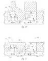
- FIG. 1shows a number of vias 101 - 1 , 101 - 2 , 101 - 3 , . . . , 101 -N are formed in an insulator material 103 , e.g. silicon dioxide (SiO 2 ), contacting with a substrate 100 .
- an insulator material 103e.g. silicon dioxide (SiO 2 )
- SiO 2silicon dioxide
- any number of semiconductor devicese.g. 105 A and 105 B, can be formed in the substrate to which the number of vias 101 - 1 , 101 - 2 , 101 - 3 , . . . , 101 -N make electrical contact.
- FIG. 105 A and 105 Bcan be formed in the substrate to which the number of vias 101 - 1 , 101 - 2 , 101 - 3 , . . . , 101 -N make electrical contact.
- FIG. 105 A and 105 Bcan be formed in the substrate to which the number of vias
- a number of metal lines 107 - 1 , 107 - 2 , 107 - 3 , . . . , 107 -Nare sandwiched and electrically couple between the number of vias 101 - 1 , 101 - 2 , 101 - 3 , . . . , 101 -N in order to form a multilevel wiring interconnect.
- fabricatorsuse a dual-damascene metallization technique, which takes its name from the ancient Damascene metalworking art of inlaying metal in grooves or channels to form ornamental patterns.
- the dual-damascene techniqueentails covering the components on a wafer with an insulative layer 103 , etching small holes in the insulative layer 103 to expose portions of the components underneath in substrate 100 , and subsequently etching shallow trenches from hole to hole to define a number of metal lines. Fabricators then blanket the entire insulative layer with a layer of aluminum or other conductive material and polish off the excess, leaving behind conductive vias, or contact plugs, in the holes and conductive lines in the trenches.
- a metal conductive materialsuch as Aluminum can be deposited in the openings of in the insulator 103 using an electroplated metal deposition technique.
- the metal conductive materiale.g. the number of vias 101 - 1 , 101 - 2 , 101 - 3 , . . . , 101 -N and the number of metal lines 107 - 1 , 107 - 2 , 107 - 3 , . . . , 107 -N, fills the holes and the trenches.
- FIG. 1illustrates the structure after the excess metal conductive material has been removed through a chemically mechanical planarization (CMP) process step.
- CMPchemically mechanical planarization
- the purpose of this inventionis to disclose a simple method of fabricating a multi-level interconnect with copper to reduce resistance and a combination of air-gaps and low dielectric constant insulators, e.g. low-k dielectrics, to reduce capacitance.
- a selective copper deposition by electroless deposition at or near room temperatureis used, as disclosed by K. Y. Ahn and Leonard Forbes in copending and commonly assigned application Ser. No. 09/483,881, entitled “Selective Electroless-Plated Copper Metallization,” which is hereby incorporated by reference.
- FIGS. 2A-2Eillustrate an embodiment of the various processing steps for a selective electroless-plated copper metallization and multilevel wiring interconnect scheme according to the teachings of the present invention.
- a seed layer, or first seed layer, 202is deposited on a substrate 200 .
- depositing the first seed layer 202 on the substrate 200includes depositing a thin film of Palladium (Pd) on the substrate 200 .
- depositing the first seed layer 202 on the substrate 200includes depositing a thin film of Copper (Cu) on the substrate.
- the seed layer 202is deposited to have a thickness of less than 15 nanometers (nm).
- the seed layer 202is deposited to form a barely continuous film in the thickness range of 3 to 10 nm. In another embodiment, the seed layer 202 is deposited such that the seed layer possesses a discontinuous island structure in the thickness range of 3 to 10 nm. In one embodiment, the seed layer 202 is deposited using a physical vapor deposition process. For example, in one embodiment, the seed layer 202 is deposited using a sputtering deposition technique. In another embodiment, the seed layer 202 is deposited using an evaporation deposition technique.
- a physical vapor deposition processFor example, in one embodiment, the seed layer 202 is deposited using a sputtering deposition technique. In another embodiment, the seed layer 202 is deposited using an evaporation deposition technique.
- a photolithography techniqueis used to define a number of via holes, conductor openings, e.g. openings 206 - 1 and 206 - 2 , above the seed layer 202 on the substrate 200 .
- using a photolithography technique to define a number of holes 206 - 1 and 206 - 2includes patterning a photoresist layer 208 to define the number via holes, or openings 206 - 1 and 206 - 2 over the seed layer 202 .
- the manner of forming the patterned photoresist layer, or first patterned photoresist layer, 208are examples of the manner of forming the patterned photoresist layer, or first patterned photoresist layer, 208 .
- a photoresist layercan be deposited over the seed layer 202 using any suitable technique, e.g. by spin coating. Then the photoresist can be masked, exposed, and washed to define the number of via holes, or openings 206 - 1 and 206 - 2 to the seed layer 202 .
- the thickness of the photoresist layer 202is scalable. That is, the deposition of the photoresist layer 208 is controllable such that the photoresist thickness can be set at a predetermined height (h1).
- the scalable thickness of the photoresist layer 208determines a height (h1), or depth (h1) for the number of via holes, or openings 206 - 1 and 206 - 2 .
- the structureis now as shown in FIG. 2 A.
- FIG. 2Billustrates the structure after the next sequence of processing steps.
- a first conductive metal layeris deposited over the structure.
- conductive metal lines and viasother than copper, such as, aluminum, gold and silver.
- the fabrication step discussed hereinare focused on using copper for the metal lines and vias.
- a layer of copper, first layer of copper, or first level of copper vias 210is deposited over the seed layer 202 using electroless plating.
- the first layer of coppercan be a first level of copper metal lines 210 .
- the inventionis not so limited.
- the layer of copper, first layer of copper, or first level of copper vias 210can be deposited over the seed layer 202 using electroless plating.
- the layer of copper, first layer of copper, or first level of copper vias 210is formed in the number of via holes, or openings, 206 - 1 and 206 - 2 .
- depositing the layer of copper, first layer of copper, or first level of copper vias 210 over the seed layer 202is such that the layer of copper, first layer of copper, or first level of copper vias 210 form on the seed layer 202 but not on the patterned photoresist layer 208 .
- the structureis now as appears in FIG. 2 B.
- FIG. 2Cillustrates the structure following the next sequence of processing steps.
- another seed layer, or second seed layer, 216is deposited on the first layer of copper, or first level of copper vias 210 and the top surface 214 of the first patterned photoresist layer 208 .
- depositing the second seed layer 216 on the first layer of copper, or first level of copper vias 210 and the top surface 214 of the first patterned photoresist layer 208includes depositing a thin film of Palladium (Pd).
- depositing the second seed layer 216 on the first layer of copper, or first level of copper vias 210 and the top surface 214 of the first patterned photoresist layer 208includes depositing a thin film of Copper (Cu).
- the second seed layer 216is deposited to have a thickness of less than 15 nanometers (nm). In one embodiment, the second seed layer 216 is deposited to form a barely continuous film in the thickness range of 3 to 10 nm. In another embodiment, the second seed layer 216 is deposited such that the second seed layer 216 possesses a discontinuous island structure 216 having an island thickness in the range of 3 to 10 nm.
- the second seed layer 216is deposited using a physical vapor deposition process.
- the second seed layer 216is deposited using a sputtering deposition technique.
- the second seed layer 216is deposited using an evaporation deposition technique.
- a second patterned photoresist layer 218is deposited above the second seed layer 216 , which defines a number of conductor line openings, e.g. conductor line openings 220 - 1 and 220 - 2 .
- the number of conductor line openings 220 - 1 and 220 - 2are defined to form a number of conductor line openings 220 - 1 and 220 - 2 having a near minimum width and spacing.
- the photoresistcan be masked, exposed, and washed to define the number of conductor line openings 220 - 1 and 220 - 2 to the second seed layer 216 .
- the thickness of the second patterned photoresist layer 218is scalable. That is, the deposition of the photoresist layer 218 is controllable such that the photoresist thickness can be set at a predetermined height (h2).
- the scalable thickness of the second patterned photoresist layer 218determines a height (h2), or depth (h2) for the number of conductor line openings 220 - 1 and 220 - 2 .
- another layer of copper, second layer of copper, or first level of conductor lines 224is deposited or formed in the number of conductor line openings 220 - 1 and 220 - 2 using electroless plating.
- this next layer of copper, second layer of copper, or first level of conductor lines 224can be deposited in the number of conductor line openings 220 - 1 and 220 - 2 using electroless plating.
- depositing this next layer of copper, second layer of copper, or first level of conductor lines 224 over the second seed layer 216is such that this next layer of copper, second layer of copper, or first level of conductor lines 224 form on the second seed layer 216 but not on the second patterned photoresist layer 218 .
- the structureis now as appears in FIG. 2 C.
- another seed layer, or third seed layer, 229is deposited on the second layer of copper, or first level of conductor lines 224 and the top surface 226 of the second patterned photoresist layer 218 .
- depositing the third seed layer 229 on the second layer of copper, or first level of conductor lines 224 and the top surface 226 of the second patterned photoresist layer 218includes depositing a thin film of Palladium (Pd).
- depositing the third seed layer 229 on the second layer of copper, or first level of conductor lines 224 and the top surface 226 of the second patterned photoresist layer 218includes depositing a thin film of Copper (Cu).
- the third seed layer 229is deposited to have a thickness of less than 15 nanometers (nm). In one embodiment, the third seed layer 229 is deposited to form a barely continuous film in the thickness range of 3 to 10 nm. In another embodiment, the third seed layer 229 is deposited such that the third seed layer 229 possesses a discontinuous island structure 229 having an island thickness in the range of 3 to 10 nm.
- the third seed layer 229is deposited using a physical vapor deposition process.
- the third seed layer 229is deposited using a sputtering deposition technique.
- the third seed layer 229is deposited using an evaporation deposition technique.
- FIG. 2Dillustrates the structure following the next sequence of processing steps.
- a third patterned photoresist layer 230is deposited above the third seed layer 229 , which defines a number of via holes, or openings, e.g. openings 232 - 1 and 232 - 2 , to the third seed layer 229 .
- a photoresist layercan be deposited over the third seed layer 229 using any suitable technique, e.g. by spin coating.
- the photoresistcan be masked, exposed, and washed to define the number of via holes, or openings 232 - 1 and 232 - 2 to the third seed layer 229 .
- the thickness of the second patterned photoresist layer 218is scalable. That is, the deposition of the photoresist layer 230 is controllable such that the photoresist thickness can be set at a predetermined height (h3).
- the scalable thickness of the second patterned photoresist layer 230determines a height (h3) for the number of via holes, or openings 232 - 1 and 232 - 2 .
- FIG. 2Danother layer of copper, third layer of copper, or second level of copper vias 234 is deposited or formed over the third seed layer 229 using electroless plating.
- the third layer of copper, or second level of copper vias 234is formed in the number of via holes, or openings 232 - 1 and 232 - 2 to the third seed layer 229 .
- Forming the third layer of copper, or second level of copper vias 234includes filling the number of via holes, or openings 232 - 1 and 232 - 2 . According to the teachings of the present invention, depositing third layer of copper, or second level of copper vias 234 over the third seed layer 229 is such that the third layer of copper, or second level of copper vias 234 form on the third seed layer 229 but not on the third patterned photoresist layer 230 . The structure is now as appears in FIG. 2 D.
- FIG. 2Eillustrates the structure following the next sequence of processing steps.
- the first, second, and third patterned photoresist layers 208 , 218 , and 230are removed.
- removing the first, second, and third patterned photoresist layers 208 , 218 , and 230includes removing the first, second, and third patterned photoresist layers 208 , 218 , and 230 using an oxygen plasma etching.
- the methodfurther includes removing the first, second, and third seed layers, 202 , 216 , and 229 respectively, with the photoresist layers from areas on the substrate which are not beneath the number of copper vias or between the conductive metal lines and the vias.
- the seed layers, 202 , 216 , and 229can be deposited to have a thickness of less than 15 nanometers (nm), thus forming a barely continuous thin film and/or discontinuous island structure.
- Other suitable techniques for removing the first, second, and third patterned photoresist layers 208 , 218 , and 230can similarly be employed, such as soaking in a solvent bath.
- the first, second, and third patterned photoresist layers 208 , 218 , and 230can be removed at earlier or later stages of a fabrication process, as described herein, depending on the number of via and metal levels to be formed. It should be noted that a planarization process such as chemical mechanical polishing (CMP) can be employed after each level of metal deposition, if required, to provide a planar surface for the subsequent processing.
- CMPchemical mechanical polishing
- FIG. 2Fillustrates the structure following the last and most important step in the fabrication process according to the teachings of the present invention.
- this stepincludes the formation of a low dielectric constant material, or low-k dielectric 236 and, at the same time, formation of air gaps 240 - 1 , 240 - 2 , . . . , 240 -N.
- the low-k dielectric 236is deposited between the number of metal lines, e.g. 210 , 224 , and 234 , and the substrate 200 using a directional process in order to accommodate the concurrent formation of air gaps 240 - 1 , 240 - 2 , . . .
- depositing a low dielectric constant material 236 and concurrently forming air gaps 240 - 1 , 240 - 2 , . . . , 240 -Nincludes depositing a low dielectric constant material 236 having a dielectric constant (k) of less than 2.7.
- a highly directional processis used to deposit a low-k polymer film 236 .
- the area under the multilayer metal lines, 210 , 224 , and 234will become air gaps 240 - 1 , 240 - 2 , . . . , 240 -N.
- depositing a low dielectric constant material 236 between the number of metal lines 210 , 224 , and 234 and the substrate 200includes using a highly directional deposition tool.
- using a direction processincludes using a microwave plasma-assisted supersonic jet deposition technique.
- An example of this technique for use in the present inventionis described in U.S. Pat. No. 5,356,672, issued Oct. 18, 1994 to Schmitt et al., entitled “Method for microwave plasma assisted supersonic jet deposition of thin films”.
- the ordinary chemical vapor deposition (CVD) processmay not be suitable for the present invention, since the conventional CVD process typically provides conformal deposition, which will not form the air gaps 240 - 1 , 240 - 2 , . . . , 240 -N according to the teachings of the present invention.
- CVDchemical vapor deposition
- depositing a low dielectric constant material 236includes depositing an organic silica film 236 .
- depositing a low dielectric constant materialincludes the deposition of an extremely low dielectric constant organic silica films 236 such as described in an article by Y. Uchida et al., entitled “A fluorinated Organic-Silica Film with Extremely Low Dielectric Constant,” Japan J. Appl. Phys., 38, no. 4B, p. 2368-2372 (1999). The same is incorporated herein by reference.
- This embodimentincludes depositing a fluorinated organic-silica film 236 using a quasi hydrogen-free chemical vapor deposition process.
- using a quasi hydrogen-free chemical vapor deposition processincludes using a mixture of tetra-iso-cyanate silane, di-methyl silyl di-iso-cyanate silane, and tri-methyl amine by successive fluorination.
- using a mixture of tetra-iso-cyanate silane, di-methyl silyl di-iso-cyanate silane, and tri-methyl amine by successive fluorinationincludes creating a film 236 in which a set of methyl groups and a flouring group of atoms are as much as 43% and 9% respectively of that for a content of silicon atoms in the film 236 .
- a film 236has good insulting characteristics and a dielectric constant (k) as low as 2.5.
- depositing a low dielectric constant material 236includes forming a low dielectric constant film by radio frequency plasma enhanced chemical vapor deposition using tetramethylsilane.
- a low dielectric constant filmby radio frequency plasma enhanced chemical vapor deposition using tetramethylsilane.
- A. Grill and V. Patelentitled “Low dielectric constant films prepared by plasma-enhanced chemical vapor deposition from tetramethylsilane,” Journal of Applied Physics, 85, no. 6, p. 3314-3318 (1999) which is incorporated herein by reference.
- dielectric constants (k) as low as 3.1can be obtained in annealed films.
- depositing a low dielectric constant material 236includes forming a polymer-like organic thin film 236 between the number of metal lines, e.g. 210 , 224 , and 234 , and the substrate 200 using a plasma enhanced CVD process using a para-xylene precursor.
- a plasma enhanced CVD processusing a para-xylene precursor.
- the relative dielectric constant (k) of this polymer-like organic thin film 236increased from 2.7 to 3.21.
- the film 236 deposited at a higher plasma powershowed higher thermal stability.
- the film 236 deposited at 60 Wwas stable up to 450° C., and all films 236 were insulating under an applied electric field up to as large as 1 MegaVolts/cm.
- any one or combination of the above described methodsare suitable for performing the methods of the present invention to create the novel multilevel wiring interconnect such that the structure includes a low dielectric constant material 236 and a number of air gaps 240 - 1 , 240 - 2 , . . . , 240 -N formed between the number of metal lines, e.g. 210 , 224 , and 234 , and the substrate 200 .
- the sameare not intended to limit the scope of the present invention.
- One of ordinary skill in the artwill further understand upon reading this disclosure, that prior to the directional deposition of the low-k dielectric 236 the number of metal lines, e.g.
- 210 , 224 , and 234can be exposed to a dilute silane at approximately 300 degrees Celsius to form a surface silicide as a passivation layer in order to prevent reaction of a copper metal line, e.g. 210 , 224 , and 234 , and polymer film 236 .
- a copper metal linee.g. 210 , 224 , and 234
- polymer film 236e.g. a copper metal line
- One method for forming the sameis described in an article by S. Hymes et al., entitled “Passivation of Copper by Silicide Formation in Dilute Silane,” MRS Conference Proceedings , ULSI-VII, p. 425-431 (1992) which is incorporated herein by reference.
- any excess material on top of multilevel wiring interconnect of the present inventioncan be removed by etching, such as by chemical mechanical polishing (CMP) in order to provide a planarized, smooth surface for subsequent processing.
- CMPchemical mechanical polishing
- FIG. 3is an illustration of an integrated circuit 301 formed according to the teachings of the present invention.
- integrated circuit 301is part of an integrated memory circuit.
- the integrated circuit 301includes a multilevel wiring interconnect having a number of multilayer metal lines, e.g. 310 , 324 , and 334 , connecting to a number of semiconductor devices, e.g. one or more transistors 305 A and 305 B, in a substrate 300 .
- the number of multilayer metal lines, e.g. 310 , 324 , and 334 , in integrated circuit 301includes a multilayer copper wiring structure. As shown in FIG.
- the integrated circuit 301includes a low dielectric constant insulator 336 in a number of interstices between the number of copper lines, 310 , 324 , and 334 , and the substrate 300 .
- the integrated circuitincludes a number of air gaps 340 - 1 , 340 - 2 , . . . , 340 -N in the low dielectric constant insulator 336 .
- the embodiment shown in FIG. 3illustrates that a multilayer wiring interconnect which has been planarized, such as by a CMP process, to provide a planarized, smooth surface for subsequent processing.
- FIG. 4illustrates a system 400 having an integrated memory circuit 430 and incorporating a multilevel wiring structure formed according to the teachings of the present invention.
- this system 400includes a processor 410 and an integrated circuit, or integrated memory circuit 430 coupled to the processor 410 .
- the processor 410can be coupled to the integrated memory circuit 430 via any suitable bus 420 , as the same are known and understood by one of ordinary skill in the art.
- the processor 410 and integrated circuit 430are located on a single wafer or die.
- at least a portion of the integrated circuit 430includes a multilevel wiring structure as disclosed in the various embodiments provided herein.
Landscapes
- Engineering & Computer Science (AREA)
- Physics & Mathematics (AREA)
- Condensed Matter Physics & Semiconductors (AREA)
- General Physics & Mathematics (AREA)
- Computer Hardware Design (AREA)
- Microelectronics & Electronic Packaging (AREA)
- Power Engineering (AREA)
- Manufacturing & Machinery (AREA)
- Internal Circuitry In Semiconductor Integrated Circuit Devices (AREA)
Abstract
Description
This application is a Divisional of U.S. application Ser. No. 10/093,244 filed Mar. 6, 2002 which is a Divisional of U.S. application Ser. No. 09/583,514 filed May 31,2000 now issued as U.S. Pat. No. 6,423,629, which are incorporated herein by reference.
This application is related to the following co-pending and commonly assigned application; application Ser. No. 09/483,881, entitled “Selective Electroless-Plated Copper Metallization,” which is hereby incorporated by reference.
The present invention relates generally to integrated circuits. More particularly, it pertains to structures and methods for multilevel copper interconnects with low-k dielectric constants and air gaps.
As the integrated circuit (IC) technology makes rapid progress toward 100 mm gate transistors, the speed limiting factor is no longer the transistor delay, but the RC delay associated with the metal interconnects. A great deal of work is being done in this area on new and innovative materials and fabrication techniques to reduce the capacitance and thus reduce RC delay of interconnects. Currently studied low-k dielectrics include fluorinated silicon dioxide (SiO2), aerogels, and polymers. Additionally, as IC technology continues to scale, the aspect ratio of metal lines increases and the intra-level line-to-line capacitance increasingly dominates over the inter-level capacitance. Thus, it becomes increasingly important to implement low-k schemes between tightly spaced metal lines and less so between metal levels.
One approach to reducing the RC delay is provided in copending and commonly assigned application; application Ser. No. 09/483,881, entitled “Selective Electroless-Plated Copper Metallization,” which is hereby incorporated by reference. Further, an article by B. Shieh et al., entitled “Air-Gap Formation During IMD Deposition to Lower Interconnect Capacitance,”IEEE Electron Devices Letters,19, no. 1, p. 16-18 (1998) presented simulations and some initial experimental results showing the possible capacitance reduction achievable using air-gap structures.
Another approach is described in an article by T. Ueda et al., entitled “A Novel Air Gap Integration Scheme for Multi-level Interconnects using Self-aligned Via Plugs,” 1998 Symposium on VLSI Technology,Digest of Technical Papers, p. 46-47 (1998) in which an air-gap structure was introduced between lines and SiO2was provided between metal levels. As described in this article, an effective dielectric constant of 1.8 at 0.3 micrometer (μm) line spacing was obtained. The authors of this article used the combination of PE-CVD SiO2with poor step coverage characteristics to intentionally form the air gaps, and biased HDP-CVD SiO2with good filling capability for the formation of inter-metal dielectric (IMD). In another approach described by J. G. Fleming et al., entitled “Use of Air Gap Structures to Lower Intra-level Capacitance,”Proceedings of1997Dielectrics for ULSI Multi-level Interconnect Conference, p. 139 (1997) a process of fabricating air-gap structures to lower intra-level capacitance was introduced. The authors of this article used an oxide deposition process with poor step coverage to create the desired air gaps. Yet another approach is described in U.S. Pat. No. 5,900,668, by D. L. Wollesen, entitled “Low Capacitance Interconnection,” issued May 4, 1999, which describes a scheme in which the parasitic capacitance is reduced by removing sections of dielectric inter-layers by anisotropic etching to form air-gaps which can remain or be filled with another dielectric material with a lower dielectric constant. An example of a prior art multilevel metallization scheme according to this process is provided in FIG.1.
Still, all of these approaches either involve complex additional processing steps or fail to provide an added benefit of reducing both intral-level line to line capacitance and the inter-level capacitance. Accordingly, there remains a need in the art to provide streamlined, improved methods and structures for alleviating the capacitance problems associated with via and metal line fabrication processes as design rules shrink.
The above mentioned problems associated with integrated circuit size and performance, the via and metal line formation process, and other problems are addressed by the present invention and will be understood by reading and studying the following specification. Structures and methods are provided which include a selective electroless copper metallization. The present invention provides for a multilayer copper wiring structure by electroless, selectively deposited copper in a streamlined process which further reduces both intra-level line to line capacitance and the inter-level capacitance.
In particular, an illustrative embodiment of the present invention includes a novel methodology for forming multilevel wiring interconnects in an integrated circuit assembly. The method includes forming a number of multilayer metal lines, e.g. copper lines formed by selective electroless plating, separated by air gaps above a substrate. A low dielectric constant material is deposited between the number of metal lines and the substrate using a directional process. According to the teachings of the present invention, using a directional process includes maintaining a number of air gaps in the low dielectric constant material.
In one embodiment, depositing a low dielectric constant material includes depositing an organic silica film. In one embodiment, depositing a low dielectric constant material between the number of metal lines and the substrate using a directional process includes using a microwave plasma-assisted supersonic jet deposition process. In another, depositing a low dielectric constant material between the number of metal lines and the substrate using a directional process includes using a quasi hydrogen-free chemical vapor deposition process. In another, depositing a low dielectric constant material includes forming a low dielectric constant film by radio frequency plasma enhanced chemical vapor deposition using tetramethylsilane. In still another, depositing a low dielectric constant material includes depositing a polymer-like organic thin film by plasma-enhance chemical vapor deposition using a para-xylene precursor.
These and other embodiments, aspects, advantages, and features of the present invention will be set forth in part in the description which follows, and in part will become apparent to those skilled in the art by reference to the following description of the invention and referenced drawings or by practice of the invention. The aspects, advantages, and features of the invention are realized and attained by means of the instrumentalities, procedures, and combinations particularly pointed out in the appended claims.
The following detailed description of the preferred embodiments can best be understood when read in conjunction with the following drawings, in which:
In the following detailed description of the invention, reference is made to the accompanying drawings which form a part hereof, and in which is shown, by way of illustration, specific embodiments in which the invention may be practiced. These embodiments are described in sufficient detail to enable those skilled in the art to practice the invention. Other embodiments may be utilized and structural, logical, and electrical changes may be made without departing from the scope of the present invention.
The terms wafer and substrate used in the following description include any structure having an exposed surface with which to form the integrated circuit (IC) structure of the invention. The term substrate is understood to include semiconductor wafers. The term substrate is also used to refer to semiconductor structures during processing, and may include other layers that have been fabricated thereupon. Substrate includes doped and undoped semiconductors, epitaxial semiconductor layers supported by a base semiconductor or insulator, as well as other semiconductor structures well known to one skilled in the art. The term insulator is defined to include any material that is less electrically conductive than the materials generally referred to as conductors by those skilled in the art. The following detailed description is, therefore, not to be taken in a limiting sense.
The prior art inFIG. 1 , shows a number of vias101-1,101-2,101-3, . . . ,101-N are formed in aninsulator material 103, e.g. silicon dioxide (SiO2), contacting with asubstrate 100. As one of ordinary skill in the art will recognize, any number of semiconductor devices, e.g.105A and105B, can be formed in the substrate to which the number of vias101-1,101-2,101-3, . . . ,101-N make electrical contact. Also, as shown inFIG. 1 , a number of metal lines107-1,107-2,107-3, . . . ,107-N are sandwiched and electrically couple between the number of vias101-1,101-2,101-3, . . . ,101-N in order to form a multilevel wiring interconnect.
Conventionally, to form vias and aluminum wire metal lines, fabricators use a dual-damascene metallization technique, which takes its name from the ancient Damascene metalworking art of inlaying metal in grooves or channels to form ornamental patterns. The dual-damascene technique entails covering the components on a wafer with aninsulative layer 103, etching small holes in theinsulative layer 103 to expose portions of the components underneath insubstrate 100, and subsequently etching shallow trenches from hole to hole to define a number of metal lines. Fabricators then blanket the entire insulative layer with a layer of aluminum or other conductive material and polish off the excess, leaving behind conductive vias, or contact plugs, in the holes and conductive lines in the trenches.
As shown in the prior art ofFIG. 1 , a metal conductive material such as Aluminum can be deposited in the openings of in theinsulator 103 using an electroplated metal deposition technique. As shown inFIG. 1 , the metal conductive material, e.g. the number of vias101-1,101-2,101-3, . . . ,101-N and the number of metal lines107-1,107-2,107-3, . . . ,107-N, fills the holes and the trenches.
The purpose of this invention is to disclose a simple method of fabricating a multi-level interconnect with copper to reduce resistance and a combination of air-gaps and low dielectric constant insulators, e.g. low-k dielectrics, to reduce capacitance. According to one embodiment of the present invention, a selective copper deposition by electroless deposition at or near room temperature is used, as disclosed by K. Y. Ahn and Leonard Forbes in copending and commonly assigned application Ser. No. 09/483,881, entitled “Selective Electroless-Plated Copper Metallization,” which is hereby incorporated by reference.
A photolithography technique is used to define a number of via holes, conductor openings, e.g. openings206-1 and206-2, above theseed layer 202 on thesubstrate 200. As one of ordinary skill in the art will understand upon reading this disclosure, using a photolithography technique to define a number of holes206-1 and206-2, includes patterning aphotoresist layer 208 to define the number via holes, or openings206-1 and206-2 over theseed layer 202. One of ordinary skill in the art will also understand upon reading this disclosure, the manner of forming the patterned photoresist layer, or first patterned photoresist layer,208. For example, a photoresist layer can be deposited over theseed layer 202 using any suitable technique, e.g. by spin coating. Then the photoresist can be masked, exposed, and washed to define the number of via holes, or openings206-1 and206-2 to theseed layer 202. One of ordinary skill in the art will further understand, upon reading this disclosure, that the thickness of thephotoresist layer 202 is scalable. That is, the deposition of thephotoresist layer 208 is controllable such that the photoresist thickness can be set at a predetermined height (h1). Thus, the scalable thickness of thephotoresist layer 208 determines a height (h1), or depth (h1) for the number of via holes, or openings206-1 and206-2. The structure is now as shown in FIG.2A.
In one embodiment, thesecond seed layer 216 is deposited using a physical vapor deposition process. For example, in one embodiment, thesecond seed layer 216 is deposited using a sputtering deposition technique. In another embodiment, thesecond seed layer 216 is deposited using an evaporation deposition technique. One of ordinary skill in the art will understand, upon reading this disclosure, the manner in which such physical vapor deposition processes can be performed to form thesecond seed layer 216 described herein.
A secondpatterned photoresist layer 218 is deposited above thesecond seed layer 216, which defines a number of conductor line openings, e.g. conductor line openings220-1 and220-2. In one embodiment, depositing the secondpatterned photoresist layer 218 which defines a number of conductor line openings220-1 and220-2, or first level metal line openings. In one embodiment, the number of conductor line openings220-1 and220-2 are defined to form a number of conductor line openings220-1 and220-2 having a near minimum width and spacing. As one of ordinary skill in the art will understand upon reading this disclosure, this insures a sufficient space in the structure for a subsequent removal of the photoresist layers, e.g. first patternedphotoresist layer 208, on lower levels. This consideration is also discussed in copending and commonly assigned application; application Ser. No. 09/483,881, entitled “Selective Electroless-Plated Copper Metallization,” which is hereby incorporated by reference. One of ordinary skill in the art will understand upon reading this disclosure, the manner of forming the secondpatterned photoresist layer 218. For example, a photoresist layer can be deposited over thesecond seed layer 216 using any suitable technique, e.g. by spin coating. Then the photoresist can be masked, exposed, and washed to define the number of conductor line openings220-1 and220-2 to thesecond seed layer 216. One of ordinary skill in the art will further understand, upon reading this disclosure, that the thickness of the secondpatterned photoresist layer 218 is scalable. That is, the deposition of thephotoresist layer 218 is controllable such that the photoresist thickness can be set at a predetermined height (h2). Thus, the scalable thickness of the secondpatterned photoresist layer 218 determines a height (h2), or depth (h2) for the number of conductor line openings220-1 and220-2.
As shown inFIG. 2C , another layer of copper, second layer of copper, or first level ofconductor lines 224 is deposited or formed in the number of conductor line openings220-1 and220-2 using electroless plating. One of ordinary skill in the art will understand upon reading this disclosure the various manner in which this next layer of copper, second layer of copper, or first level ofconductor lines 224 can be deposited in the number of conductor line openings220-1 and220-2 using electroless plating. According to the teachings of the present invention depositing this next layer of copper, second layer of copper, or first level ofconductor lines 224 over thesecond seed layer 216 is such that this next layer of copper, second layer of copper, or first level ofconductor lines 224 form on thesecond seed layer 216 but not on the secondpatterned photoresist layer 218. The structure is now as appears in FIG.2C.
Next, as shown inFIG. 2C , another seed layer, or third seed layer,229 is deposited on the second layer of copper, or first level ofconductor lines 224 and thetop surface 226 of the secondpatterned photoresist layer 218. In one embodiment, depositing thethird seed layer 229 on the second layer of copper, or first level ofconductor lines 224 and thetop surface 226 of the secondpatterned photoresist layer 218 includes depositing a thin film of Palladium (Pd). In another embodiment, depositing thethird seed layer 229 on the second layer of copper, or first level ofconductor lines 224 and thetop surface 226 of the secondpatterned photoresist layer 218 includes depositing a thin film of Copper (Cu). Again in one embodiment, thethird seed layer 229 is deposited to have a thickness of less than 15 nanometers (nm). In one embodiment, thethird seed layer 229 is deposited to form a barely continuous film in the thickness range of 3 to 10 nm. In another embodiment, thethird seed layer 229 is deposited such that thethird seed layer 229 possesses adiscontinuous island structure 229 having an island thickness in the range of 3 to 10 nm.
In one embodiment, thethird seed layer 229 is deposited using a physical vapor deposition process. For example, in one embodiment, thethird seed layer 229 is deposited using a sputtering deposition technique. In another embodiment, thethird seed layer 229 is deposited using an evaporation deposition technique. One of ordinary skill in the art will understand, upon reading this disclosure, the manner in which such physical vapor deposition processes can be performed to form thethird seed layer 229 described herein.
InFIG. 2D , another layer of copper, third layer of copper, or second level ofcopper vias 234 is deposited or formed over thethird seed layer 229 using electroless plating. One of ordinary skill in the art will understand upon reading this disclosure the various manner in which the third layer of copper, or second level ofcopper vias 234 can be deposited over thethird seed layer 229 using electroless plating. According to the teachings of the present invention, the third layer of copper, or second level ofcopper vias 234 is formed in the number of via holes, or openings232-1 and232-2 to thethird seed layer 229. Forming the third layer of copper, or second level ofcopper vias 234 includes filling the number of via holes, or openings232-1 and232-2. According to the teachings of the present invention, depositing third layer of copper, or second level ofcopper vias 234 over thethird seed layer 229 is such that the third layer of copper, or second level ofcopper vias 234 form on thethird seed layer 229 but not on the thirdpatterned photoresist layer 230. The structure is now as appears in FIG.2D.
The following descriptions illustrate, by way of example and not by way of limitation, that according to the teachings of the present invention, several polymer source materials can be used. In one embodiment, depositing a low dielectricconstant material 236 includes depositing anorganic silica film 236. In one example depositing a low dielectric constant material includes the deposition of an extremely low dielectric constantorganic silica films 236 such as described in an article by Y. Uchida et al., entitled “A fluorinated Organic-Silica Film with Extremely Low Dielectric Constant,”Japan J. Appl. Phys.,38, no. 4B, p. 2368-2372 (1999). The same is incorporated herein by reference. This embodiment includes depositing a fluorinated organic-silica film 236 using a quasi hydrogen-free chemical vapor deposition process. In one embodiment, using a quasi hydrogen-free chemical vapor deposition process includes using a mixture of tetra-iso-cyanate silane, di-methyl silyl di-iso-cyanate silane, and tri-methyl amine by successive fluorination. In one embodiment, using a mixture of tetra-iso-cyanate silane, di-methyl silyl di-iso-cyanate silane, and tri-methyl amine by successive fluorination includes creating afilm 236 in which a set of methyl groups and a flouring group of atoms are as much as 43% and 9% respectively of that for a content of silicon atoms in thefilm 236. Such afilm 236 has good insulting characteristics and a dielectric constant (k) as low as 2.5. In one embodiment, the method further includes vacuum annealing thisfilm 236. Vacuum annealing can improve the dielectric constant of this film to approximately k=2.1.
In another embodiment, according to the teachings of the present invention, depositing a low dielectricconstant material 236 includes forming a low dielectric constant film by radio frequency plasma enhanced chemical vapor deposition using tetramethylsilane. One embodiment for performing the same is described in an article by A. Grill and V. Patel, entitled “Low dielectric constant films prepared by plasma-enhanced chemical vapor deposition from tetramethylsilane,” Journal of Applied Physics, 85, no. 6, p. 3314-3318 (1999) which is incorporated herein by reference. In this embodiment, dielectric constants (k) as low as 3.1 can be obtained in annealed films.
In another embodiment, according to the teachings of the present invention, depositing a low dielectricconstant material 236 includes forming a polymer-like organicthin film 236 between the number of metal lines, e.g.210,224, and234, and thesubstrate 200 using a plasma enhanced CVD process using a para-xylene precursor. One embodiment for performing the same is described in an article by Y. C. Quan et al., entitled “Polymer-like Organic thin films Deposited by Plasma Enhanced Chemical Vapor Deposition Using the Para-xylene Precursor as Low dielectric constant Interlayer Dielectrics for Multilevel Metallization,”Japan J. Appl. Phys.,38, no.3A, p. 1356-1358 (1999) which is incorporated herein by reference. According to this embodiment, as the plasma power is increased from 5 Watts (W) to 60 W, the relative dielectric constant (k) of this polymer-like organicthin film 236 increased from 2.7 to 3.21. However, thefilm 236 deposited at a higher plasma power showed higher thermal stability. Thefilm 236 deposited at 60 W was stable up to 450° C., and allfilms 236 were insulating under an applied electric field up to as large as 1 MegaVolts/cm.
Again, as one of ordinary skill in the art will understand upon reading this disclosure, any one or combination of the above described methods are suitable for performing the methods of the present invention to create the novel multilevel wiring interconnect such that the structure includes a low dielectricconstant material 236 and a number of air gaps240-1,240-2, . . . ,240-N formed between the number of metal lines, e.g.210,224, and234, and thesubstrate 200. The same are not intended to limit the scope of the present invention. One of ordinary skill in the art will further understand upon reading this disclosure, that prior to the directional deposition of the low-k dielectric 236 the number of metal lines, e.g.210,224, and234, can be exposed to a dilute silane at approximately 300 degrees Celsius to form a surface silicide as a passivation layer in order to prevent reaction of a copper metal line, e.g.210,224, and234, andpolymer film 236. One method for forming the same is described in an article by S. Hymes et al., entitled “Passivation of Copper by Silicide Formation in Dilute Silane,”MRS Conference Proceedings, ULSI-VII, p. 425-431 (1992) which is incorporated herein by reference. Another method is described in a co-pending, co-filed and commonly assigned application; attorney docket number 303.685US1, entitled “Multilevel Copper Interconnect with Double Insulation,” which is incorporated by reference. One of ordinary skill in the art will understand upon reading this disclosure, that the choice of such a passivation layer is dependant in part upon thedielectric materials 236 used.
Any excess material on top of multilevel wiring interconnect of the present invention can be removed by etching, such as by chemical mechanical polishing (CMP) in order to provide a planarized, smooth surface for subsequent processing. As one of ordinary skill in the art will understand upon reading this disclosure, forming additional or subsequent layer/levels of conductive vias and metallization lines are also included within the scope of the present invention.
Thus, structures and methods have been shown which provide for a multilayer copper wiring structure by electroless, selectively deposited copper in a streamlined process which further reduces both intral-level line to line capacitance and the intra-level capacitance.
Although specific embodiments have been illustrated and described herein, it will be appreciated by those of ordinary skill in the art that any arrangement which is calculated to achieve the same purpose may be substituted for the specific embodiment shown. This application is intended to cover any adaptations or variations of the present invention. It is to be understood that the above description is intended to be illustrative, and not restrictive. The scope of the invention includes any other applications in which the above structures and fabrication methods are used. The scope of the invention should be determined with reference to the appended claims, along with the full scope of equivalents to which such claims are entitled.
Claims (15)
1. A multilevel wiring interconnect in an integrated circuit, comprising:
a number of multilayer metal lines connecting to a number of silicon devices in a substrate;
a low dielectric constant insulator in a number of interstices between the number of multilayer metal lines and the substrate;
wherein the low dielectric constant insulator includes a number of air gaps in the low dielectric constant material; and
wherein the low dielectric constant insulator includes a film in which of a set of methyl groups and a fluorine group of atoms are as much as 43% and 9% respectively of that for a content of silicon atoms in the film.
2. The multilevel wiring interconnect ofclaim 1 , wherein the low dielectric constant insulator includes a low dielectric constant organic silica film.
3. The multilevel wiring interconnect ofclaim 1 , wherein the low dielectric constant insulator includes a low dielectric constant insulator having a dielectric constant (k) of less than 2.7.
4. The multilevel wiring interconnect ofclaim 1 , wherein the number of multilayer metal lines includes a number of multilayer metal lines selected from the group consisting of Aluminum, Copper, Silver, and Gold.
5. The multilevel wiring interconnect ofclaim 1 , wherein the number of multilayer metal lines includes a first conductor bridge level.
6. A multilevel wiring interconnect system, comprising:
a number of multilayer metal lines connecting to a number of integrated circuit devices in a substrate;
a low dielectric constant insulator in a number of interstices between the number of multilayer metal lines and the substrate, the low dielectric constant insulator having a number of air gaps therein; and
wherein the low dielectric constant insulator includes a film in which of a set of methyl groups and a fluorine group of atoms are as much as 43% and 9% respectively of that for a content of silicon atoms in the film.
7. The system ofclaim 6 , wherein the number of multilayer metal lines are adapted to connect to at least one of a processor and a memory.
8. The system ofclaim 6 , wherein the substrate is a die.
9. The system of claim, wherein the substrate includes a silicon.
10. The system ofclaim 6 , wherein the number of multilayer metal lines consist essentially of copper.
11. A system having a multilevel wiring interconnect, comprising:
an integrated circuit device; and
an integrated memory circuit operably coupled to the integrated circuit device, wherein the integrated memory circuit includes a multilevel wiring interconnect, the multilevel wiring interconnect comprising:
a number of multilayer Copper lines connecting to one or more of the transistors in a substrate;
a low dielectric constant insulator in a number of interstices between the number of multilayer Copper lines and the substrate;
wherein the low dielectric constant insulator includes a number of air gaps in the low dielectric constant material; and
wherein the low dielectric constant insulator includes a film in which of a set of methyl groups and a fluorine group of atoms are as much as 43% and 9% respectively of that for a content of silicon atoms in the film.
12. The system ofclaim 11 , wherein the integrated circuit device includes a processor.
13. A system, comprising:
a processor; and
an integrated memory circuit coupled to the processor, wherein the integrated memory circuit further includes a multilevel wiring interconnect, the multilevel wiring interconnect comprising:
a number of multilayer Copper lines connecting to one or more of the transistors in a substrate;
a low dielectric constant insulator in a number of interstices between the number of multilayer Copper lines and the substrate;
wherein the low dielectric constant insulator includes a number of air gaps in the low dielectric constant material; and
wherein the low dielectric constant insulator includes a film in which of a set of methyl groups and a fluorine group of atoms are as much as 43% and 9% respectively of that for a content of silicon atoms in the film.
14. The system ofclaim 13 , wherein the low dielectric constant insulator includes a low dielectric constant organic silica film.
15. The system ofclaim 13 , wherein the low dielectric constant insulator includes a low dielectric constant insulator having a dielectric constant of less than 2.7.
Priority Applications (1)
| Application Number | Priority Date | Filing Date | Title |
|---|---|---|---|
| US10/786,354US6995470B2 (en) | 2000-05-31 | 2004-02-25 | Multilevel copper interconnects with low-k dielectrics and air gaps |
Applications Claiming Priority (3)
| Application Number | Priority Date | Filing Date | Title |
|---|---|---|---|
| US09/583,514US6423629B1 (en) | 2000-05-31 | 2000-05-31 | Multilevel copper interconnects with low-k dielectrics and air gaps |
| US10/093,244US7091611B2 (en) | 2000-05-31 | 2002-03-06 | Multilevel copper interconnects with low-k dielectrics and air gaps |
| US10/786,354US6995470B2 (en) | 2000-05-31 | 2004-02-25 | Multilevel copper interconnects with low-k dielectrics and air gaps |
Related Parent Applications (1)
| Application Number | Title | Priority Date | Filing Date |
|---|---|---|---|
| US10/093,244DivisionUS7091611B2 (en) | 2000-05-31 | 2002-03-06 | Multilevel copper interconnects with low-k dielectrics and air gaps |
Publications (2)
| Publication Number | Publication Date |
|---|---|
| US20040164419A1 US20040164419A1 (en) | 2004-08-26 |
| US6995470B2true US6995470B2 (en) | 2006-02-07 |
Family
ID=24333406
Family Applications (3)
| Application Number | Title | Priority Date | Filing Date |
|---|---|---|---|
| US09/583,514Expired - LifetimeUS6423629B1 (en) | 2000-05-31 | 2000-05-31 | Multilevel copper interconnects with low-k dielectrics and air gaps |
| US10/093,244Expired - Fee RelatedUS7091611B2 (en) | 2000-05-31 | 2002-03-06 | Multilevel copper interconnects with low-k dielectrics and air gaps |
| US10/786,354Expired - Fee RelatedUS6995470B2 (en) | 2000-05-31 | 2004-02-25 | Multilevel copper interconnects with low-k dielectrics and air gaps |
Family Applications Before (2)
| Application Number | Title | Priority Date | Filing Date |
|---|---|---|---|
| US09/583,514Expired - LifetimeUS6423629B1 (en) | 2000-05-31 | 2000-05-31 | Multilevel copper interconnects with low-k dielectrics and air gaps |
| US10/093,244Expired - Fee RelatedUS7091611B2 (en) | 2000-05-31 | 2002-03-06 | Multilevel copper interconnects with low-k dielectrics and air gaps |
Country Status (1)
| Country | Link |
|---|---|
| US (3) | US6423629B1 (en) |
Cited By (10)
| Publication number | Priority date | Publication date | Assignee | Title |
|---|---|---|---|---|
| US20080116581A1 (en)* | 2003-10-15 | 2008-05-22 | Megica Corporation | Post passivation interconnection schemes on top of the ic chips |
| US20090001510A1 (en)* | 2007-06-29 | 2009-01-01 | Phillip D Matz | Air gap in integrated circuit inductor fabrication |
| US8242014B2 (en) | 2005-03-11 | 2012-08-14 | Renesas Electronics Corporation | Method for manufacturing a semiconductor device having an interconnect structure and a reinforcing insulating film |
| US8497203B2 (en) | 2010-08-13 | 2013-07-30 | International Business Machines Corporation | Semiconductor structures and methods of manufacture |
| US8525339B2 (en) | 2011-07-27 | 2013-09-03 | International Business Machines Corporation | Hybrid copper interconnect structure and method of fabricating same |
| US8969132B2 (en) | 2010-09-20 | 2015-03-03 | Nuvotronics, Llc | Device package and methods for the fabrication thereof |
| US9053948B2 (en) | 2013-04-22 | 2015-06-09 | Samsung Electronics Co., Ltd. | Semiconductor devices |
| US9312203B2 (en) | 2013-01-02 | 2016-04-12 | Globalfoundries Inc. | Dual damascene structure with liner |
| US9337152B2 (en) | 2013-03-15 | 2016-05-10 | Nuvotronics, Inc | Formulation for packaging an electronic device and assemblies made therefrom |
| US20220037389A1 (en)* | 2015-03-31 | 2022-02-03 | Sony Semiconductor Solutions Corporation | Solid-state image-capturing element and electronic device |
Families Citing this family (70)
| Publication number | Priority date | Publication date | Assignee | Title |
|---|---|---|---|---|
| US6093623A (en)* | 1998-08-04 | 2000-07-25 | Micron Technology, Inc. | Methods for making silicon-on-insulator structures |
| US6423613B1 (en) | 1998-11-10 | 2002-07-23 | Micron Technology, Inc. | Low temperature silicon wafer bond process with bulk material bond strength |
| US6555467B2 (en)* | 2001-09-28 | 2003-04-29 | Sharp Laboratories Of America, Inc. | Method of making air gaps copper interconnect |
| US6514808B1 (en)* | 2001-11-30 | 2003-02-04 | Motorola, Inc. | Transistor having a high K dielectric and short gate length and method therefor |
| US20080121343A1 (en)* | 2003-12-31 | 2008-05-29 | Microfabrica Inc. | Electrochemical Fabrication Methods Incorporating Dielectric Materials and/or Using Dielectric Substrates |
| US7517462B2 (en)* | 2003-06-27 | 2009-04-14 | Microfabrica Inc. | Electrochemical fabrication methods incorporating dielectric materials and/or using dielectric substrates |
| KR100450681B1 (en)* | 2002-08-16 | 2004-10-02 | 삼성전자주식회사 | Capacitor of semiconductor memory device and manufacturing method thereof |
| JP4574145B2 (en)* | 2002-09-13 | 2010-11-04 | ローム・アンド・ハース・エレクトロニック・マテリアルズ,エル.エル.シー. | Air gap formation |
| US6949456B2 (en)* | 2002-10-31 | 2005-09-27 | Asm Japan K.K. | Method for manufacturing semiconductor device having porous structure with air-gaps |
| US7449407B2 (en)* | 2002-11-15 | 2008-11-11 | United Microelectronics Corporation | Air gap for dual damascene applications |
| US6917109B2 (en)* | 2002-11-15 | 2005-07-12 | United Micorelectronics, Corp. | Air gap structure and formation method for reducing undesired capacitive coupling between interconnects in an integrated circuit device |
| US7138329B2 (en)* | 2002-11-15 | 2006-11-21 | United Microelectronics Corporation | Air gap for tungsten/aluminum plug applications |
| US20040232552A1 (en)* | 2002-12-09 | 2004-11-25 | Advanced Micro Devices, Inc. | Air gap dual damascene process and structure |
| US7071532B2 (en)* | 2003-09-30 | 2006-07-04 | International Business Machines Corporation | Adjustable self-aligned air gap dielectric for low capacitance wiring |
| DE102004003337A1 (en)* | 2004-01-22 | 2005-08-18 | Infineon Technologies Ag | Plasma enhanced chemical vapor deposition method, silicon-oxygen-nitrogen containing material and layer assembly |
| US7094669B2 (en)* | 2004-08-03 | 2006-08-22 | Chartered Semiconductor Manufacturing Ltd | Structure and method of liner air gap formation |
| US20060035457A1 (en)* | 2004-08-10 | 2006-02-16 | Carter Richard J | Interconnection capacitance reduction |
| DE102004050391B4 (en)* | 2004-10-15 | 2007-02-08 | Infineon Technologies Ag | Method for producing a layer arrangement and layer arrangement |
| KR20060073189A (en)* | 2004-12-24 | 2006-06-28 | 동부일렉트로닉스 주식회사 | Copper wiring formation method of semiconductor device |
| US7531444B2 (en)* | 2005-02-11 | 2009-05-12 | International Business Machines Corporation | Method to create air gaps using non-plasma processes to damage ILD materials |
| US7977032B2 (en)* | 2005-02-11 | 2011-07-12 | International Business Machines Corporation | Method to create region specific exposure in a layer |
| DE102005008476B4 (en)* | 2005-02-24 | 2006-12-21 | Infineon Technologies Ag | Guideway arrangement and associated production method |
| JP5204370B2 (en)* | 2005-03-17 | 2013-06-05 | ルネサスエレクトロニクス株式会社 | Semiconductor device and manufacturing method thereof |
| US7247560B1 (en)* | 2006-03-01 | 2007-07-24 | Gary Neal Poovey | Selective deposition of double damascene metal |
| EP1835050A1 (en)* | 2006-03-15 | 2007-09-19 | Doniar S.A. | Process for the fabrication of LIGA-UV multilayer metallic structures, the layers being adjacent and not completely superimposed, and structure therefrom. |
| US20080073795A1 (en)* | 2006-09-24 | 2008-03-27 | Georgia Tech Research Corporation | Integrated circuit interconnection devices and methods |
| KR100829603B1 (en)* | 2006-11-23 | 2008-05-14 | 삼성전자주식회사 | Method for manufacturing a semiconductor device having an air gap |
| FR2910706B1 (en)* | 2006-12-21 | 2009-03-20 | Commissariat Energie Atomique | INTERCONNECTION ELEMENT BASED ON CARBON NANOTUBES |
| US7608538B2 (en) | 2007-01-05 | 2009-10-27 | International Business Machines Corporation | Formation of vertical devices by electroplating |
| US7973409B2 (en) | 2007-01-22 | 2011-07-05 | International Business Machines Corporation | Hybrid interconnect structure for performance improvement and reliability enhancement |
| US7651891B1 (en)* | 2007-08-09 | 2010-01-26 | National Semiconductor Corporation | Integrated circuit package with stress reduction |
| KR101382564B1 (en)* | 2008-05-28 | 2014-04-10 | 삼성전자주식회사 | Method for formation of interlayer dielectric having air gap |
| US8058138B2 (en) | 2008-07-17 | 2011-11-15 | Micron Technology, Inc. | Gap processing |
| JP5491077B2 (en)* | 2009-06-08 | 2014-05-14 | キヤノン株式会社 | Semiconductor device and manufacturing method of semiconductor device |
| US8519540B2 (en)* | 2009-06-16 | 2013-08-27 | International Business Machines Corporation | Self-aligned dual damascene BEOL structures with patternable low- K material and methods of forming same |
| US8659115B2 (en)* | 2009-06-17 | 2014-02-25 | International Business Machines Corporation | Airgap-containing interconnect structure with improved patternable low-K material and method of fabricating |
| US8163658B2 (en)* | 2009-08-24 | 2012-04-24 | International Business Machines Corporation | Multiple patterning using improved patternable low-k dielectric materials |
| US8202783B2 (en) | 2009-09-29 | 2012-06-19 | International Business Machines Corporation | Patternable low-k dielectric interconnect structure with a graded cap layer and method of fabrication |
| US8637395B2 (en)* | 2009-11-16 | 2014-01-28 | International Business Machines Corporation | Methods for photo-patternable low-k (PPLK) integration with curing after pattern transfer |
| US8367540B2 (en)* | 2009-11-19 | 2013-02-05 | International Business Machines Corporation | Interconnect structure including a modified photoresist as a permanent interconnect dielectric and method of fabricating same |
| US8642252B2 (en) | 2010-03-10 | 2014-02-04 | International Business Machines Corporation | Methods for fabrication of an air gap-containing interconnect structure |
| US8896120B2 (en) | 2010-04-27 | 2014-11-25 | International Business Machines Corporation | Structures and methods for air gap integration |
| US8241992B2 (en) | 2010-05-10 | 2012-08-14 | International Business Machines Corporation | Method for air gap interconnect integration using photo-patternable low k material |
| US8373271B2 (en) | 2010-05-27 | 2013-02-12 | International Business Machines Corporation | Interconnect structure with an oxygen-doped SiC antireflective coating and method of fabrication |
| US8890318B2 (en) | 2011-04-15 | 2014-11-18 | International Business Machines Corporation | Middle of line structures |
| US9054160B2 (en) | 2011-04-15 | 2015-06-09 | International Business Machines Corporation | Interconnect structure and method for fabricating on-chip interconnect structures by image reversal |
| US8900988B2 (en) | 2011-04-15 | 2014-12-02 | International Business Machines Corporation | Method for forming self-aligned airgap interconnect structures |
| US8575000B2 (en) | 2011-07-19 | 2013-11-05 | SanDisk Technologies, Inc. | Copper interconnects separated by air gaps and method of making thereof |
| US8822137B2 (en) | 2011-08-03 | 2014-09-02 | International Business Machines Corporation | Self-aligned fine pitch permanent on-chip interconnect structures and method of fabrication |
| US20130062732A1 (en) | 2011-09-08 | 2013-03-14 | International Business Machines Corporation | Interconnect structures with functional components and methods for fabrication |
| US8519482B2 (en)* | 2011-09-28 | 2013-08-27 | Globalfoundries Singapore Pte. Ltd. | Reliable contacts |
| US8779592B2 (en) | 2012-05-01 | 2014-07-15 | Taiwan Semiconductor Manufacturing Company, Ltd. | Via-free interconnect structure with self-aligned metal line interconnections |
| US9087753B2 (en) | 2012-05-10 | 2015-07-21 | International Business Machines Corporation | Printed transistor and fabrication method |
| KR102003881B1 (en)* | 2013-02-13 | 2019-10-17 | 삼성전자주식회사 | Semiconductor deivces and methods of fabricating the same |
| US9343400B2 (en)* | 2013-03-13 | 2016-05-17 | Taiwan Semiconductor Manufacturing Company, Ltd. | Dual damascene gap filling process |
| US9159671B2 (en) | 2013-11-19 | 2015-10-13 | International Business Machines Corporation | Copper wire and dielectric with air gaps |
| KR102092863B1 (en) | 2013-12-30 | 2020-03-24 | 삼성전자주식회사 | Semiconductor device and method of fabricating the same |
| US9548333B2 (en)* | 2014-09-25 | 2017-01-17 | Qualcomm Incorporated | MRAM integration with low-K inter-metal dielectric for reduced parasitic capacitance |
| US9312167B1 (en) | 2014-10-03 | 2016-04-12 | Applied Materials, Inc. | Air-gap structure formation with ultra low-k dielectric layer on PECVD low-k chamber |
| JP6856974B2 (en)* | 2015-03-31 | 2021-04-14 | ソニーセミコンダクタソリューションズ株式会社 | Solid-state image sensor and electronic equipment |
| US9818642B2 (en) | 2015-04-15 | 2017-11-14 | Nxp Usa, Inc. | Method of forming inter-level dielectric structures on semiconductor devices |
| WO2016209246A1 (en)* | 2015-06-25 | 2016-12-29 | Intel Corporation | Doric pillar supported maskless airgap structure for capacitance benefit with unlanded via solution |
| US9627316B1 (en)* | 2015-12-15 | 2017-04-18 | Taiwan Semiconductor Manufacturing Co., Ltd. | Field effect transistor devices having interconnect structures and manufacturing method thereof |
| US10727114B2 (en) | 2017-01-13 | 2020-07-28 | International Business Machines Corporation | Interconnect structure including airgaps and substractively etched metal lines |
| US10211052B1 (en)* | 2017-09-22 | 2019-02-19 | Lam Research Corporation | Systems and methods for fabrication of a redistribution layer to avoid etching of the layer |
| US11361993B2 (en)* | 2018-12-14 | 2022-06-14 | Tokyo Electron Limited | Method for inverse via patterning for back end of line dual damascene structures |
| US10985051B2 (en)* | 2019-07-24 | 2021-04-20 | Nanya Technology Corporation | Semiconductor device with air spacer and method for forming the same |
| US11587870B2 (en)* | 2019-08-13 | 2023-02-21 | Micron Technology, Inc. | Apparatus comprising aluminum interconnections, memory devices comprising interconnections, and related methods |
| CN115188728A (en)* | 2019-12-06 | 2022-10-14 | 中国科学院微电子研究所 | Metallization stack, method of making same, and electronic device including metallization stack |
| US20230215615A1 (en)* | 2022-01-06 | 2023-07-06 | Ferric Inc. | Multi-Layered Metal Frame Power Package |
Citations (230)
| Publication number | Priority date | Publication date | Assignee | Title |
|---|---|---|---|---|
| US1254987A (en) | 1917-10-15 | 1918-01-29 | Cooper Res Company | Alloy. |
| US1976375A (en) | 1931-01-27 | 1934-10-09 | Beryllium Corp | Beryllium-aluminum alloy and method of heat treating the same |
| US2244608A (en) | 1939-02-09 | 1941-06-03 | Cooper Wilford Beryllium Ltd | Process of making alloys of aluminum beryllium |
| US2842438A (en) | 1956-08-02 | 1958-07-08 | American Metal Climax Inc | Copper-zirconium alloys |
| US3147110A (en) | 1961-11-27 | 1964-09-01 | Dow Chemical Co | Die-expressed article of aluminum-base alloy and method of making |
| US3337334A (en) | 1963-12-06 | 1967-08-22 | Lockheed Aircraft Corp | Beryllium-aluminum alloy |
| US3506438A (en) | 1967-07-24 | 1970-04-14 | Mallory & Co Inc P R | Method of producing beryllium composites by liquid phase sintering |
| US3548948A (en) | 1969-01-23 | 1970-12-22 | Mallory & Co Inc P R | Procedure for chill casting beryllium composite |
| US3548915A (en) | 1969-06-11 | 1970-12-22 | Mallory & Co Inc P R | New procedure for chill casting beryllium composite |
| US3687737A (en) | 1970-07-17 | 1972-08-29 | Mallory & Co Inc P R | Method of making beryllium-aluminum-copper-silicon wrought material |
| US3832456A (en) | 1962-10-18 | 1974-08-27 | Ethyl Corp | Process for the manufacture of beryllium hydride |
| US3923500A (en) | 1971-08-11 | 1975-12-02 | Toyo Valve Co Ltd | Copper base alloy |
| US3932226A (en) | 1974-12-06 | 1976-01-13 | Rca Corporation | Method of electrically interconnecting semiconductor elements |
| US3954570A (en) | 1974-11-11 | 1976-05-04 | Amp Incorporated | Sensitized polyimides and circuit elements thereof |
| US4022931A (en) | 1974-07-01 | 1977-05-10 | Motorola, Inc. | Process for making semiconductor device |
| US4029377A (en) | 1976-02-03 | 1977-06-14 | Rogers Corporation | Push-on bus bar |
| US4065330A (en) | 1974-09-26 | 1977-12-27 | The Foundation: The Research Institute Of Electric And Magnetic Alloys | Wear-resistant high-permeability alloy |
| US4101855A (en) | 1976-11-05 | 1978-07-18 | Hi-G Incorporated | Miniature relay |
| US4158719A (en) | 1977-06-09 | 1979-06-19 | Carpenter Technology Corporation | Low expansion low resistivity composite powder metallurgy member and method of making the same |
| US4213818A (en) | 1979-01-04 | 1980-07-22 | Signetics Corporation | Selective plasma vapor etching process |
| US4233066A (en) | 1972-04-27 | 1980-11-11 | Aktiebolaget Elektrokoppar | Electrical conductor of aluminium |
| US4314594A (en) | 1977-02-26 | 1982-02-09 | Vacuumschmelze Gmbh | Reducing magnetic hysteresis losses in cores of thin tapes of soft magnetic amorphous metal alloys |
| US4386116A (en) | 1981-12-24 | 1983-05-31 | International Business Machines Corporation | Process for making multilayer integrated circuit substrate |
| US4389429A (en) | 1980-06-16 | 1983-06-21 | Rockwell International Corporation | Method of forming integrated circuit chip transmission line |
| US4394223A (en) | 1981-10-06 | 1983-07-19 | The United States Of America As Represented By The Secretary Of The Air Force | Tin and gold plating process |
| US4423547A (en) | 1981-06-01 | 1984-01-03 | International Business Machines Corporation | Method for forming dense multilevel interconnection metallurgy for semiconductor devices |
| US4561173A (en) | 1978-11-14 | 1985-12-31 | U.S. Philips Corporation | Method of manufacturing a wiring system |
| US4565157A (en) | 1983-03-29 | 1986-01-21 | Genus, Inc. | Method and apparatus for deposition of tungsten silicides |
| US4574095A (en) | 1984-11-19 | 1986-03-04 | International Business Machines Corporation | Selective deposition of copper |
| US4670297A (en) | 1985-06-21 | 1987-06-02 | Raytheon Company | Evaporated thick metal and airbridge interconnects and method of manufacture |
| US4709359A (en) | 1982-06-28 | 1987-11-24 | Magnovox Government And Industrial Electronics Company | End weighted reed sound transducer |
| US4762728A (en) | 1985-04-09 | 1988-08-09 | Fairchild Semiconductor Corporation | Low temperature plasma nitridation process and applications of nitride films formed thereby |
| US4788082A (en) | 1984-02-13 | 1988-11-29 | Schmitt Jerome J | Method and apparatus for the deposition of solid films of a material from a jet stream entraining the gaseous phase of said material |
| US4847111A (en) | 1988-06-30 | 1989-07-11 | Hughes Aircraft Company | Plasma-nitridated self-aligned tungsten system for VLSI interconnections |
| US4857481A (en) | 1989-03-14 | 1989-08-15 | Motorola, Inc. | Method of fabricating airbridge metal interconnects |
| US4931410A (en) | 1987-08-25 | 1990-06-05 | Hitachi, Ltd. | Process for producing semiconductor integrated circuit device having copper interconnections and/or wirings, and device produced |
| US4948459A (en) | 1988-01-20 | 1990-08-14 | U.S. Philips Corporation | Method of enabling electrical connection to a substructure forming part of an electronic device |
| US4962058A (en) | 1989-04-14 | 1990-10-09 | International Business Machines Corporation | Process for fabricating multi-level integrated circuit wiring structure from a single metal deposit |
| US4996584A (en) | 1985-01-31 | 1991-02-26 | Gould, Inc. | Thin-film electrical connections for integrated circuits |
| US5019531A (en) | 1988-05-23 | 1991-05-28 | Nippon Telegraph And Telephone Corporation | Process for selectively growing thin metallic film of copper or gold |
| US5034799A (en) | 1989-02-22 | 1991-07-23 | Kabushiki Kaisha Toshiba | Semiconductor integrated circuit device having a hollow multi-layered lead structure |
| US5045635A (en) | 1989-06-16 | 1991-09-03 | Schlegel Corporation | Conductive gasket with flame and abrasion resistant conductive coating |
| US5084412A (en) | 1989-10-02 | 1992-01-28 | Kabushiki Kaisha Toshiba | Method of manufacturing a semiconductor device with a copper wiring layer |
| US5100499A (en) | 1989-12-20 | 1992-03-31 | Texas Instruments Incorporated | Copper dry etch process using organic and amine radicals |
| US5130274A (en) | 1991-04-05 | 1992-07-14 | International Business Machines Corporation | Copper alloy metallurgies for VLSI interconnection structures |
| US5148260A (en) | 1989-09-07 | 1992-09-15 | Kabushiki Kaisha Toshiba | Semiconductor device having an improved air-bridge lead structure |
| US5149615A (en) | 1991-01-08 | 1992-09-22 | The Boeing Company | Method for producing a planar surface on which a conductive layer can be applied |
| US5158986A (en) | 1991-04-05 | 1992-10-27 | Massachusetts Institute Of Technology | Microcellular thermoplastic foamed with supercritical fluid |
| US5173442A (en) | 1990-07-23 | 1992-12-22 | Microelectronics And Computer Technology Corporation | Methods of forming channels and vias in insulating layers |
| US5227658A (en) | 1991-10-23 | 1993-07-13 | International Business Machines Corporation | Buried air dielectric isolation of silicon islands |
| US5231036A (en) | 1990-12-07 | 1993-07-27 | Kyocera America, Inc. | Method of using a contamination shield during the manufacture of EPROM semiconductor package windows |
| US5231056A (en) | 1992-01-15 | 1993-07-27 | Micron Technology, Inc. | Tungsten silicide (WSix) deposition process for semiconductor manufacture |
| US5232866A (en) | 1991-10-23 | 1993-08-03 | International Business Machines Corporation | Isolated films using an air dielectric |
| US5240878A (en) | 1991-04-26 | 1993-08-31 | International Business Machines Corporation | Method for forming patterned films on a substrate |
| US5243222A (en) | 1991-04-05 | 1993-09-07 | International Business Machines Corporation | Copper alloy metallurgies for VLSI interconnection structures |
| JPH05267643A (en) | 1992-03-19 | 1993-10-15 | Fujitsu Ltd | Semiconductor device and manufacturing method thereof |
| US5256205A (en) | 1990-05-09 | 1993-10-26 | Jet Process Corporation | Microwave plasma assisted supersonic gas jet deposition of thin film materials |
| US5268315A (en) | 1992-09-04 | 1993-12-07 | Tektronix, Inc. | Implant-free heterojunction bioplar transistor integrated circuit process |
| US5308440A (en) | 1991-09-05 | 1994-05-03 | Matsushita Electric Industrial Co., Ltd. | Method of making semiconductor device with air-bridge interconnection |
| US5324683A (en) | 1993-06-02 | 1994-06-28 | Motorola, Inc. | Method of forming a semiconductor structure having an air region |
| US5324684A (en) | 1992-02-25 | 1994-06-28 | Ag Processing Technologies, Inc. | Gas phase doping of semiconductor material in a cold-wall radiantly heated reactor under reduced pressure |
| US5336914A (en) | 1991-06-19 | 1994-08-09 | Nec Corporation | Static semiconductor memory device |
| US5354712A (en) | 1992-11-12 | 1994-10-11 | Northern Telecom Limited | Method for forming interconnect structures for integrated circuits |
| US5356672A (en) | 1990-05-09 | 1994-10-18 | Jet Process Corporation | Method for microwave plasma assisted supersonic gas jet deposition of thin films |
| US5371042A (en) | 1992-06-16 | 1994-12-06 | Applied Materials, Inc. | Method of filling contacts in semiconductor devices |
| US5384284A (en) | 1993-10-01 | 1995-01-24 | Micron Semiconductor, Inc. | Method to form a low resistant bond pad interconnect |
| US5399897A (en) | 1993-11-29 | 1995-03-21 | Raytheon Company | Microstructure and method of making such structure |
| US5408742A (en) | 1991-10-28 | 1995-04-25 | Martin Marietta Corporation | Process for making air bridges for integrated circuits |
| US5413962A (en) | 1994-07-15 | 1995-05-09 | United Microelectronics Corporation | Multi-level conductor process in VLSI fabrication utilizing an air bridge |
| US5413687A (en) | 1991-11-27 | 1995-05-09 | Rogers Corporation | Method for metallizing fluoropolymer substrates |
| US5424030A (en) | 1992-12-03 | 1995-06-13 | Yamaha Metanix Corporation | Copper alloy for fine pattern lead frame |
| US5426330A (en) | 1992-02-26 | 1995-06-20 | International Business Machines Corporation | Refractory metal capped low resistivity metal conductor lines and vias |
| US5442237A (en) | 1991-10-21 | 1995-08-15 | Motorola Inc. | Semiconductor device having a low permittivity dielectric |
| US5444015A (en) | 1992-12-15 | 1995-08-22 | International Business Machines Corporation | Larce scale IC personalization method employing air dielectric structure for extended conductors |
| JPH0778815B2 (en) | 1986-09-19 | 1995-08-23 | 富士通株式会社 | Voting ticket automatic refund machine |
| US5447887A (en) | 1994-04-01 | 1995-09-05 | Motorola, Inc. | Method for capping copper in semiconductor devices |
| US5457344A (en) | 1994-03-25 | 1995-10-10 | Bartelink; Dirk J. | Test fixtures for C4 solder-bump technology |
| US5470789A (en) | 1993-03-19 | 1995-11-28 | Fujitsu Limited | Process for fabricating integrated circuit devices |
| US5470801A (en) | 1993-06-28 | 1995-11-28 | Lsi Logic Corporation | Low dielectric constant insulation layer for integrated circuit structure and method of making same |
| JPH07321111A (en) | 1994-05-26 | 1995-12-08 | Meidensha Corp | Method of forming electroless plated interconnection for integrated circuit |
| US5476817A (en) | 1994-05-31 | 1995-12-19 | Texas Instruments Incorporated | Method of making reliable metal leads in high speed LSI semiconductors using both dummy leads and thermoconductive layers |
| US5485037A (en) | 1993-04-12 | 1996-01-16 | Amkor Electronics, Inc. | Semiconductor device having a thermal dissipator and electromagnetic shielding |
| US5495667A (en) | 1994-11-07 | 1996-03-05 | Micron Technology, Inc. | Method for forming contact pins for semiconductor dice and interconnects |
| US5506449A (en) | 1993-03-24 | 1996-04-09 | Kawasaki Steel Corporation | Interconnection structure for semiconductor integrated circuit and manufacture of the same |
| US5529956A (en) | 1991-07-23 | 1996-06-25 | Nec Corporation | Multi-layer wiring structure in semiconductor device and method for manufacturing the same |
| US5534731A (en) | 1994-10-28 | 1996-07-09 | Advanced Micro Devices, Incorporated | Layered low dielectric constant technology |
| US5538922A (en) | 1991-06-03 | 1996-07-23 | Motorola, Inc. | Method for forming contact to a semiconductor device |
| US5539227A (en) | 1993-11-24 | 1996-07-23 | Mitsubishi Denki Kabushiki Kaisha | Multi-layer wiring |
| US5539060A (en) | 1993-07-30 | 1996-07-23 | Nippon Zeon Co., Ltd. | Method for hydrogenation of metathesis polymers |
| US5578146A (en) | 1991-10-02 | 1996-11-26 | Brush Wellman, Inc. | Aluminum-beryllium alloys having high stiffness and low thermal expansion for memory devices |
| US5595937A (en) | 1995-04-13 | 1997-01-21 | Nec Corporation | Method for fabricating semiconductor device with interconnections buried in trenches |
| US5609721A (en) | 1994-03-11 | 1997-03-11 | Fujitsu Limited | Semiconductor device manufacturing apparatus and its cleaning method |
| US5625232A (en) | 1994-07-15 | 1997-04-29 | Texas Instruments Incorporated | Reliability of metal leads in high speed LSI semiconductors using dummy vias |
| US5635253A (en) | 1994-08-30 | 1997-06-03 | International Business Machines Corporation | Method of replenishing electroless gold plating baths |
| US5654245A (en) | 1993-03-23 | 1997-08-05 | Sharp Microelectronics Technology, Inc. | Implantation of nucleating species for selective metallization and products thereof |
| US5662788A (en) | 1996-06-03 | 1997-09-02 | Micron Technology, Inc. | Method for forming a metallization layer |
| US5667600A (en) | 1991-10-02 | 1997-09-16 | Brush Wellman, Inc. | Aluminum alloys containing beryllium and investment casting of such alloys |
| US5668398A (en) | 1994-05-27 | 1997-09-16 | Texas Instruments Incorporated | Multilevel interconnect structure with air gaps formed between metal leads |
| US5670420A (en) | 1994-12-05 | 1997-09-23 | Hyundai Electronics Industries Co., Ltd. | Method of forming metal interconnection layer of semiconductor device |
| US5674787A (en) | 1996-01-16 | 1997-10-07 | Sematech, Inc. | Selective electroless copper deposited interconnect plugs for ULSI applications |
| US5679608A (en) | 1994-12-21 | 1997-10-21 | Advanced Micro Devices, Inc. | Processing techniques for achieving production-worthy, low dielectric, low dielectric, low interconnect resistance and high performance IC |
| US5681441A (en) | 1992-12-22 | 1997-10-28 | Elf Technologies, Inc. | Method for electroplating a substrate containing an electroplateable pattern |
| US5695810A (en) | 1996-11-20 | 1997-12-09 | Cornell Research Foundation, Inc. | Use of cobalt tungsten phosphide as a barrier material for copper metallization |
| US5705425A (en) | 1992-05-28 | 1998-01-06 | Fujitsu Limited | Process for manufacturing semiconductor devices separated by an air-bridge |
| US5719089A (en) | 1996-06-21 | 1998-02-17 | Vanguard International Semiconductor Corporation | Method for etching polymer-assisted reduced small contacts for ultra large scale integration semiconductor devices |
| US5719410A (en) | 1993-12-28 | 1998-02-17 | Kabushiki Kaisha Toshiba | Semiconductor device wiring or electrode |
| US5725689A (en) | 1994-03-28 | 1998-03-10 | Nippon Steel Corporation | Steel wire of high strength excellent in fatigue characteristics |
| US5739579A (en) | 1992-06-29 | 1998-04-14 | Intel Corporation | Method for forming interconnections for semiconductor fabrication and semiconductor device having such interconnections |
| US5763953A (en) | 1993-01-05 | 1998-06-09 | Kabushiki Kaisha Toshiba | Semiconductor device and method of manufacturing the same |
| US5780358A (en) | 1996-04-08 | 1998-07-14 | Chartered Semiconductor Manufacturing Ltd. | Method for chemical-mechanical polish (CMP) planarizing of cooper containing conductor layers |
| US5785570A (en) | 1994-07-26 | 1998-07-28 | Pixtech S.A. | Anode for a flat display screen |
| US5792706A (en) | 1996-06-05 | 1998-08-11 | Advanced Micro Devices, Inc. | Interlevel dielectric with air gaps to reduce permitivity |
| US5792522A (en) | 1996-09-18 | 1998-08-11 | Intel Corporation | High density plasma physical vapor deposition |
| US5801098A (en) | 1996-09-03 | 1998-09-01 | Motorola, Inc. | Method of decreasing resistivity in an electrically conductive layer |
| US5814557A (en) | 1996-05-20 | 1998-09-29 | Motorola, Inc. | Method of forming an interconnect structure |
| US5821168A (en) | 1997-07-16 | 1998-10-13 | Motorola, Inc. | Process for forming a semiconductor device |
| US5824599A (en) | 1996-01-16 | 1998-10-20 | Cornell Research Foundation, Inc. | Protected encapsulation of catalytic layer for electroless copper interconnect |
| US5852871A (en) | 1993-11-16 | 1998-12-29 | Form Factor, Inc. | Method of making raised contacts on electronic components |
| US5858877A (en) | 1992-07-28 | 1999-01-12 | Micron Technology, Inc. | Self-aligned process for making contacts to silicon substrates during the manufacture of integrated circuits therein |
| US5880018A (en) | 1996-10-07 | 1999-03-09 | Motorola Inc. | Method for manufacturing a low dielectric constant inter-level integrated circuit structure |
| US5891804A (en) | 1996-04-18 | 1999-04-06 | Texas Instruments Incorporated | Process for conductors with selective deposition |
| US5891797A (en) | 1997-10-20 | 1999-04-06 | Micron Technology, Inc. | Method of forming a support structure for air bridge wiring of an integrated circuit |
| US5893752A (en) | 1997-12-22 | 1999-04-13 | Motorola, Inc. | Process for forming a semiconductor device |
| US5895740A (en) | 1996-11-13 | 1999-04-20 | Vanguard International Semiconductor Corp. | Method of forming contact holes of reduced dimensions by using in-situ formed polymeric sidewall spacers |
| US5897370A (en) | 1994-08-05 | 1999-04-27 | International Business Machines Corporation | High aspect ratio low resistivity lines/vias by surface diffusion |
| US5900668A (en) | 1995-11-30 | 1999-05-04 | Advanced Micro Devices, Inc. | Low capacitance interconnection |
| US5907772A (en) | 1996-02-26 | 1999-05-25 | Nec Corporation | Method of producing cylindrical storage node of stacked capacitor in memory cell |
| US5911113A (en) | 1997-03-18 | 1999-06-08 | Applied Materials, Inc. | Silicon-doped titanium wetting layer for aluminum plug |
| US5913147A (en) | 1997-01-21 | 1999-06-15 | Advanced Micro Devices, Inc. | Method for fabricating copper-aluminum metallization |
| US5925930A (en) | 1996-05-21 | 1999-07-20 | Micron Technology, Inc. | IC contacts with palladium layer and flexible conductive epoxy bumps |
| US5930669A (en) | 1997-04-03 | 1999-07-27 | International Business Machines Corporation | Continuous highly conductive metal wiring structures and method for fabricating the same |
| US5930596A (en) | 1994-03-29 | 1999-07-27 | Siemens Aktiengesellschaft | Semiconductor component for vertical integration and manufacturing method |
| US5932928A (en) | 1997-07-03 | 1999-08-03 | Micron Technology, Inc. | Semiconductor circuit interconnections and methods of making such interconnections |
| US5933758A (en) | 1997-05-12 | 1999-08-03 | Motorola, Inc. | Method for preventing electroplating of copper on an exposed surface at the edge exclusion of a semiconductor wafer |
| US5940733A (en) | 1995-05-03 | 1999-08-17 | Applied Materials, Inc. | Method of making polysilicon/tungsten silicide multilayer composite on an integrated circuit structure |
| US5948467A (en) | 1998-07-24 | 1999-09-07 | Sharp Laboratories Of America, Inc. | Enhanced CVD copper adhesion by two-step deposition process |
| US5962923A (en) | 1995-08-07 | 1999-10-05 | Applied Materials, Inc. | Semiconductor device having a low thermal budget metal filling and planarization of contacts, vias and trenches |
| US5969422A (en) | 1997-05-15 | 1999-10-19 | Advanced Micro Devices, Inc. | Plated copper interconnect structure |
| US5968333A (en) | 1998-04-07 | 1999-10-19 | Advanced Micro Devices, Inc. | Method of electroplating a copper or copper alloy interconnect |
| US5972804A (en) | 1997-08-05 | 1999-10-26 | Motorola, Inc. | Process for forming a semiconductor device |
| US5972179A (en) | 1997-09-30 | 1999-10-26 | Lucent Technologies Inc. | Silicon IC contacts using composite TiN barrier layer |
| US5976710A (en) | 1991-08-05 | 1999-11-02 | International Business Machines Corporation | Low TCE polyimides as improved insulator in multilayer interconnect structures |
| US5981350A (en) | 1998-05-29 | 1999-11-09 | Micron Technology, Inc. | Method for forming high capacitance memory cells |
| US5985759A (en) | 1998-02-24 | 1999-11-16 | Applied Materials, Inc. | Oxygen enhancement of ion metal plasma (IMP) sputter deposited barrier layers |
| US5989623A (en) | 1997-08-19 | 1999-11-23 | Applied Materials, Inc. | Dual damascene metallization |
| US5994776A (en) | 1996-01-11 | 1999-11-30 | Advanced Micro Devices, Inc. | Interlevel dielectric with multiple air gaps between conductive lines of an integrated circuit |
| US6001730A (en) | 1997-10-20 | 1999-12-14 | Motorola, Inc. | Chemical mechanical polishing (CMP) slurry for polishing copper interconnects which use tantalum-based barrier layers |
| US6004884A (en) | 1996-02-15 | 1999-12-21 | Lam Research Corporation | Methods and apparatus for etching semiconductor wafers |
| US6008117A (en) | 1996-03-29 | 1999-12-28 | Texas Instruments Incorporated | Method of forming diffusion barriers encapsulating copper |
| US6015465A (en) | 1998-04-08 | 2000-01-18 | Applied Materials, Inc. | Temperature control system for semiconductor process chamber |
| US6015738A (en) | 1994-05-05 | 2000-01-18 | California Institute Of Technology | Method for fabricating transistorless, multistable current-mode memory cells and memory arrays |
| US6017820A (en) | 1998-07-17 | 2000-01-25 | Cutek Research, Inc. | Integrated vacuum and plating cluster system |
| EP0304046B1 (en) | 1987-08-19 | 2000-01-26 | Fujitsu Limited | A method of stripping a resist mask |
| US6022802A (en) | 1999-03-18 | 2000-02-08 | Taiwan Semiconductor Manufacturing Company | Low dielectric constant intermetal dielectric (IMD) by formation of air gap between metal lines |
| US6025261A (en) | 1998-04-29 | 2000-02-15 | Micron Technology, Inc. | Method for making high-Q inductive elements |
| US6030877A (en) | 1997-10-06 | 2000-02-29 | Industrial Technology Research Institute | Electroless gold plating method for forming inductor structures |
| US6037248A (en) | 1997-06-13 | 2000-03-14 | Micron Technology, Inc. | Method of fabricating integrated circuit wiring with low RC time delay |
| US6054172A (en) | 1997-08-22 | 2000-04-25 | Micron Technology, Inc. | Copper electroless deposition on a titanium-containing surface |
| US6057226A (en) | 1997-11-25 | 2000-05-02 | Intel Corporation | Air gap based low dielectric constant interconnect structure and method of making same |
| US6059553A (en)* | 1996-12-17 | 2000-05-09 | Texas Instruments Incorporated | Integrated circuit dielectrics |
| US6065424A (en) | 1995-12-19 | 2000-05-23 | Cornell Research Foundation, Inc. | Electroless deposition of metal films with spray processor |
| US6069068A (en) | 1997-05-30 | 2000-05-30 | International Business Machines Corporation | Sub-quarter-micron copper interconnections with improved electromigration resistance and reduced defect sensitivity |
| US6071810A (en) | 1996-12-24 | 2000-06-06 | Kabushiki Kaisha Toshiba | Method of filling contact holes and wiring grooves of a semiconductor device |
| US6075278A (en) | 1997-04-24 | 2000-06-13 | Micron Technology, Inc. | Aluminum based alloy bridge structure and method of forming same |
| US6075287A (en) | 1997-04-03 | 2000-06-13 | International Business Machines Corporation | Integrated, multi-chip, thermally conductive packaging device and methodology |
| US6091475A (en) | 1996-12-19 | 2000-07-18 | Shin-Etsu Polymer Co., Ltd. | Connector for display inspection of a liquid crystal display panel and method for the preparation thereof |
| US6091136A (en) | 1997-06-19 | 2000-07-18 | Micron Technology, Inc. | Plastic lead frames for semiconductor devices |
| US6121126A (en) | 1998-02-25 | 2000-09-19 | Micron Technologies, Inc. | Methods and structures for metal interconnections in integrated circuits |
| US6140456A (en) | 1997-10-24 | 2000-10-31 | Quester Techology, Inc. | Chemicals and processes for making fluorinated poly(para-xylylenes) |
| US6140228A (en) | 1997-11-13 | 2000-10-31 | Cypress Semiconductor Corporation | Low temperature metallization process |
| US6139699A (en) | 1997-05-27 | 2000-10-31 | Applied Materials, Inc. | Sputtering methods for depositing stress tunable tantalum and tantalum nitride films |
| US6140234A (en) | 1998-01-20 | 2000-10-31 | International Business Machines Corporation | Method to selectively fill recesses with conductive metal |
| US6143641A (en) | 2000-01-26 | 2000-11-07 | National Semiconductor Corporation | Structure and method for controlling copper diffusion and for utilizing low K materials for copper interconnects in integrated circuit structures |
| US6143646A (en) | 1997-06-03 | 2000-11-07 | Motorola Inc. | Dual in-laid integrated circuit structure with selectively positioned low-K dielectric isolation and method of formation |
| US6150261A (en) | 1999-05-25 | 2000-11-21 | United Microelectronics Corp. | Method of fabricating semiconductor device for preventing antenna effect |
| US6153507A (en) | 1997-01-13 | 2000-11-28 | Nec Corporation | Method of fabricating semiconductor device providing effective resistance against metal layer oxidation and diffusion |
| US6159842A (en) | 1999-01-11 | 2000-12-12 | Taiwan Semiconductor Manufacturing Company | Method for fabricating a hybrid low-dielectric-constant intermetal dielectric (IMD) layer with improved reliability for multilevel interconnections |
| US6168704B1 (en) | 1999-02-04 | 2001-01-02 | Advanced Micro Device, Inc. | Site-selective electrochemical deposition of copper |
| US6171661B1 (en) | 1998-02-25 | 2001-01-09 | Applied Materials, Inc. | Deposition of copper with increased adhesion |
| US6177350B1 (en) | 1998-04-14 | 2001-01-23 | Applied Materials, Inc. | Method for forming a multilayered aluminum-comprising structure on a substrate |
| US6183564B1 (en) | 1998-11-12 | 2001-02-06 | Tokyo Electron Limited | Buffer chamber for integrating physical and chemical vapor deposition chambers together in a processing system |
| US6187656B1 (en) | 1997-10-07 | 2001-02-13 | Texas Instruments Incorporated | CVD-based process for manufacturing stable low-resistivity poly-metal gate electrodes |
| US6190732B1 (en) | 1998-09-03 | 2001-02-20 | Cvc Products, Inc. | Method and system for dispensing process gas for fabricating a device on a substrate |
| US6194233B1 (en)* | 1998-08-21 | 2001-02-27 | International Business Machines Corporation | Integrated circuit and method of manufacture for avoiding damage by electrostatic charge |
| US6197688B1 (en) | 1998-02-12 | 2001-03-06 | Motorola Inc. | Interconnect structure in a semiconductor device and method of formation |
| US6197181B1 (en) | 1998-03-20 | 2001-03-06 | Semitool, Inc. | Apparatus and method for electrolytically depositing a metal on a microelectronic workpiece |
| US6204065B1 (en) | 1997-03-27 | 2001-03-20 | Ngk Insulators, Ltd. | Conduction assist member and manufacturing method of the same |
| US6207558B1 (en) | 1999-10-21 | 2001-03-27 | Applied Materials, Inc. | Barrier applications for aluminum planarization |
| US6207553B1 (en) | 1999-01-26 | 2001-03-27 | Advanced Micro Devices, Inc. | Method of forming multiple levels of patterned metallization |
| US6208016B1 (en) | 1998-09-10 | 2001-03-27 | Micron Technology, Inc. | Forming submicron integrated-circuit wiring from gold, silver, copper and other metals |
| US6211073B1 (en) | 1998-02-27 | 2001-04-03 | Micron Technology, Inc. | Methods for making copper and other metal interconnections in integrated circuits |
| US6211561B1 (en)* | 1998-11-16 | 2001-04-03 | Conexant Systems, Inc. | Interconnect structure and method employing air gaps between metal lines and between metal layers |
| US6214719B1 (en)* | 1999-09-30 | 2001-04-10 | Novellus Systems, Inc. | Method of implementing air-gap technology for low capacitance ILD in the damascene scheme |
| US6218282B1 (en) | 1999-02-18 | 2001-04-17 | Advanced Micro Devices, Inc. | Method of forming low dielectric tungsten lined interconnection system |
| US6221763B1 (en) | 1999-04-05 | 2001-04-24 | Micron Technology, Inc. | Method of forming a metal seed layer for subsequent plating |
| US6232219B1 (en) | 1998-05-20 | 2001-05-15 | Micron Technology, Inc. | Self-limiting method of reducing contamination in a contact opening, method of making contacts and semiconductor devices therewith, and resulting structures |
| US20010002333A1 (en) | 1999-03-05 | 2001-05-31 | Chao-Yuan Huang | Method of fabricating dual damascene structure |
| US6245658B1 (en) | 1999-02-18 | 2001-06-12 | Advanced Micro Devices, Inc. | Method of forming low dielectric semiconductor device with rigid, metal silicide lined interconnection system |
| US6246118B1 (en) | 1999-02-18 | 2001-06-12 | Advanced Micro Devices, Inc. | Low dielectric semiconductor device with rigid, conductively lined interconnection system |
| US6249056B1 (en) | 1997-08-16 | 2001-06-19 | Samsung Electronics Co., Ltd. | Low resistance interconnect for a semiconductor device and method of fabricating the same |
| US6265811B1 (en) | 1996-11-29 | 2001-07-24 | Ngk Insulators, Ltd. | Ceramic element, method for producing ceramic element, display device, relay device and capacitor |
| US6265311B1 (en) | 1999-04-27 | 2001-07-24 | Tokyo Electron Limited | PECVD of TaN films from tantalum halide precursors |
| US6268276B1 (en) | 1998-12-21 | 2001-07-31 | Chartered Semiconductor Manufacturing Ltd. | Area array air gap structure for intermetal dielectric application |
| US6268277B1 (en) | 1998-01-22 | 2001-07-31 | Advanced Micro Devices, Inc. | Method of producing air gap for reducing intralayer capacitance in metal layers in damascene metalization process and product resulting therefrom |
| US6281585B1 (en) | 1997-06-30 | 2001-08-28 | Philips Electronics North America Corporation | Air gap dielectric in self-aligned via structures |
| US6284656B1 (en) | 1998-08-04 | 2001-09-04 | Micron Technology, Inc. | Copper metallurgy in integrated circuits |
| US6288905B1 (en) | 1999-04-15 | 2001-09-11 | Amerasia International Technology Inc. | Contact module, as for a smart card, and method for making same |
| US6287954B1 (en) | 1997-05-30 | 2001-09-11 | International Business Machines Corporation | Method of forming copper interconnections with enhanced electromigration resistance and reduced defect sensitivity |
| US6323553B1 (en) | 1997-02-03 | 2001-11-27 | Texas Instrument Incorporated | Reduced temperature contact/via filling |
| US6329279B1 (en) | 2000-03-20 | 2001-12-11 | United Microelectronics Corp. | Method of fabricating metal interconnect structure having outer air spacer |
| US20010054771A1 (en) | 1997-03-26 | 2001-12-27 | Wark James M. | Method for making projected contact structures for engaging bumped semiconductor devices |
| US6342448B1 (en) | 2000-05-31 | 2002-01-29 | Taiwan Semiconductor Manufacturing Company | Method of fabricating barrier adhesion to low-k dielectric layers in a copper damascene process |
| US20020014646A1 (en) | 1997-01-31 | 2002-02-07 | Robert Tsu | Integrated circuit capacitor |
| US20020028552A1 (en) | 1998-10-17 | 2002-03-07 | Ki-Young Lee | Capacitor of semiconductor integrated circuit and its fabricating method |
| US6359328B1 (en) | 1998-12-31 | 2002-03-19 | Intel Corporation | Methods for making interconnects and diffusion barriers in integrated circuits |
| US6358842B1 (en) | 2000-08-07 | 2002-03-19 | Chartered Semiconductor Manufacturing Ltd. | Method to form damascene interconnects with sidewall passivation to protect organic dielectrics |
| US6368954B1 (en) | 2000-07-28 | 2002-04-09 | Advanced Micro Devices, Inc. | Method of copper interconnect formation using atomic layer copper deposition |
| US6372622B1 (en) | 1999-10-26 | 2002-04-16 | Motorola, Inc. | Fine pitch bumping with improved device standoff and bump volume |
| US6376370B1 (en) | 2000-01-18 | 2002-04-23 | Micron Technology, Inc. | Process for providing seed layers for using aluminum, copper, gold and silver metallurgy process for providing seed layers for using aluminum, copper, gold and silver metallurgy |
| US6383920B1 (en) | 2001-01-10 | 2002-05-07 | International Business Machines Corporation | Process of enclosing via for improved reliability in dual damascene interconnects |
| US6387542B1 (en) | 2000-07-06 | 2002-05-14 | Honeywell International Inc. | Electroless silver plating |
| US6399489B1 (en) | 1999-11-01 | 2002-06-04 | Applied Materials, Inc. | Barrier layer deposition using HDP-CVD |
| US6403481B1 (en) | 1998-08-11 | 2002-06-11 | Kabushiki Kaisha Toshiba | Film formation method |
| US20020096768A1 (en) | 1995-01-03 | 2002-07-25 | International Business Machines Corporation | Soft metal conductor and method of making |
| US6429120B1 (en) | 2000-01-18 | 2002-08-06 | Micron Technology, Inc. | Methods and apparatus for making integrated-circuit wiring from copper, silver, gold, and other metals |
| US6448331B1 (en) | 1997-07-15 | 2002-09-10 | Asahi Kasei Kabushiki Kaisha | Alkoxysilane/organic polymer composition for thin insulating film production and use thereof |
| US6495445B2 (en)* | 1999-07-02 | 2002-12-17 | International Business Machines Corporation | Semi-sacrificial diamond for air dielectric formation |
| US6518198B1 (en) | 2000-08-31 | 2003-02-11 | Micron Technology, Inc. | Electroless deposition of doped noble metals and noble metal alloys |
| US6563219B2 (en) | 1999-09-02 | 2003-05-13 | Micron Technology, Inc. | Passivation integrity improvements |
| US6674167B1 (en)* | 2000-05-31 | 2004-01-06 | Micron Technology, Inc. | Multilevel copper interconnect with double passivation |
Family Cites Families (9)
| Publication number | Priority date | Publication date | Assignee | Title |
|---|---|---|---|---|
| US4591173A (en) | 1984-09-24 | 1986-05-27 | Yamaha Hatsudoki Kabushiki Kaisha | Suspension and steering mechanism for a snowmobile |
| US5323866A (en)* | 1993-03-01 | 1994-06-28 | Hydro-Quebec | Power steering system |
| US5953626A (en) | 1996-06-05 | 1999-09-14 | Advanced Micro Devices, Inc. | Dissolvable dielectric method |
| US5759906A (en)* | 1997-04-11 | 1998-06-02 | Industrial Technology Research Institute | Planarization method for intermetal dielectrics between multilevel interconnections on integrated circuits |
| US6245668B1 (en)* | 1998-09-18 | 2001-06-12 | International Business Machines Corporation | Sputtered tungsten diffusion barrier for improved interconnect robustness |
| US6342722B1 (en)* | 1999-08-05 | 2002-01-29 | International Business Machines Corporation | Integrated circuit having air gaps between dielectric and conducting lines |
| US6306750B1 (en)* | 2000-01-18 | 2001-10-23 | Taiwan Semiconductor Manufacturing Company | Bonding pad structure to prevent inter-metal dielectric cracking and to improve bondability |
| US6136680A (en)* | 2000-01-21 | 2000-10-24 | Taiwan Semiconductor Manufacturing Company | Methods to improve copper-fluorinated silica glass interconnects |
| US6413827B2 (en) | 2000-02-14 | 2002-07-02 | Paul A. Farrar | Low dielectric constant shallow trench isolation |
- 2000
- 2000-05-31USUS09/583,514patent/US6423629B1/ennot_activeExpired - Lifetime
- 2002
- 2002-03-06USUS10/093,244patent/US7091611B2/ennot_activeExpired - Fee Related
- 2004
- 2004-02-25USUS10/786,354patent/US6995470B2/ennot_activeExpired - Fee Related
Patent Citations (245)
| Publication number | Priority date | Publication date | Assignee | Title |
|---|---|---|---|---|
| US1254987A (en) | 1917-10-15 | 1918-01-29 | Cooper Res Company | Alloy. |
| US1976375A (en) | 1931-01-27 | 1934-10-09 | Beryllium Corp | Beryllium-aluminum alloy and method of heat treating the same |
| US2244608A (en) | 1939-02-09 | 1941-06-03 | Cooper Wilford Beryllium Ltd | Process of making alloys of aluminum beryllium |
| US2842438A (en) | 1956-08-02 | 1958-07-08 | American Metal Climax Inc | Copper-zirconium alloys |
| US3147110A (en) | 1961-11-27 | 1964-09-01 | Dow Chemical Co | Die-expressed article of aluminum-base alloy and method of making |
| US3832456A (en) | 1962-10-18 | 1974-08-27 | Ethyl Corp | Process for the manufacture of beryllium hydride |
| US3337334A (en) | 1963-12-06 | 1967-08-22 | Lockheed Aircraft Corp | Beryllium-aluminum alloy |
| US3506438A (en) | 1967-07-24 | 1970-04-14 | Mallory & Co Inc P R | Method of producing beryllium composites by liquid phase sintering |
| US3548948A (en) | 1969-01-23 | 1970-12-22 | Mallory & Co Inc P R | Procedure for chill casting beryllium composite |
| US3548915A (en) | 1969-06-11 | 1970-12-22 | Mallory & Co Inc P R | New procedure for chill casting beryllium composite |
| US3687737A (en) | 1970-07-17 | 1972-08-29 | Mallory & Co Inc P R | Method of making beryllium-aluminum-copper-silicon wrought material |
| US3923500A (en) | 1971-08-11 | 1975-12-02 | Toyo Valve Co Ltd | Copper base alloy |
| US4233066A (en) | 1972-04-27 | 1980-11-11 | Aktiebolaget Elektrokoppar | Electrical conductor of aluminium |
| US4022931A (en) | 1974-07-01 | 1977-05-10 | Motorola, Inc. | Process for making semiconductor device |
| US4065330A (en) | 1974-09-26 | 1977-12-27 | The Foundation: The Research Institute Of Electric And Magnetic Alloys | Wear-resistant high-permeability alloy |
| US3954570A (en) | 1974-11-11 | 1976-05-04 | Amp Incorporated | Sensitized polyimides and circuit elements thereof |
| US3932226A (en) | 1974-12-06 | 1976-01-13 | Rca Corporation | Method of electrically interconnecting semiconductor elements |
| US4029377A (en) | 1976-02-03 | 1977-06-14 | Rogers Corporation | Push-on bus bar |
| US4101855A (en) | 1976-11-05 | 1978-07-18 | Hi-G Incorporated | Miniature relay |
| US4314594A (en) | 1977-02-26 | 1982-02-09 | Vacuumschmelze Gmbh | Reducing magnetic hysteresis losses in cores of thin tapes of soft magnetic amorphous metal alloys |
| US4158719A (en) | 1977-06-09 | 1979-06-19 | Carpenter Technology Corporation | Low expansion low resistivity composite powder metallurgy member and method of making the same |
| US4561173A (en) | 1978-11-14 | 1985-12-31 | U.S. Philips Corporation | Method of manufacturing a wiring system |
| US4213818A (en) | 1979-01-04 | 1980-07-22 | Signetics Corporation | Selective plasma vapor etching process |
| US4389429A (en) | 1980-06-16 | 1983-06-21 | Rockwell International Corporation | Method of forming integrated circuit chip transmission line |
| US4423547A (en) | 1981-06-01 | 1984-01-03 | International Business Machines Corporation | Method for forming dense multilevel interconnection metallurgy for semiconductor devices |
| US4394223A (en) | 1981-10-06 | 1983-07-19 | The United States Of America As Represented By The Secretary Of The Air Force | Tin and gold plating process |
| US4386116A (en) | 1981-12-24 | 1983-05-31 | International Business Machines Corporation | Process for making multilayer integrated circuit substrate |
| US4709359A (en) | 1982-06-28 | 1987-11-24 | Magnovox Government And Industrial Electronics Company | End weighted reed sound transducer |
| US4565157A (en) | 1983-03-29 | 1986-01-21 | Genus, Inc. | Method and apparatus for deposition of tungsten silicides |
| US4788082A (en) | 1984-02-13 | 1988-11-29 | Schmitt Jerome J | Method and apparatus for the deposition of solid films of a material from a jet stream entraining the gaseous phase of said material |
| US4574095A (en) | 1984-11-19 | 1986-03-04 | International Business Machines Corporation | Selective deposition of copper |
| US4996584A (en) | 1985-01-31 | 1991-02-26 | Gould, Inc. | Thin-film electrical connections for integrated circuits |
| US4762728A (en) | 1985-04-09 | 1988-08-09 | Fairchild Semiconductor Corporation | Low temperature plasma nitridation process and applications of nitride films formed thereby |
| US4670297A (en) | 1985-06-21 | 1987-06-02 | Raytheon Company | Evaporated thick metal and airbridge interconnects and method of manufacture |
| JPH0778815B2 (en) | 1986-09-19 | 1995-08-23 | 富士通株式会社 | Voting ticket automatic refund machine |
| EP0304046B1 (en) | 1987-08-19 | 2000-01-26 | Fujitsu Limited | A method of stripping a resist mask |
| US4931410A (en) | 1987-08-25 | 1990-06-05 | Hitachi, Ltd. | Process for producing semiconductor integrated circuit device having copper interconnections and/or wirings, and device produced |
| US4948459A (en) | 1988-01-20 | 1990-08-14 | U.S. Philips Corporation | Method of enabling electrical connection to a substructure forming part of an electronic device |
| US5019531A (en) | 1988-05-23 | 1991-05-28 | Nippon Telegraph And Telephone Corporation | Process for selectively growing thin metallic film of copper or gold |
| US4847111A (en) | 1988-06-30 | 1989-07-11 | Hughes Aircraft Company | Plasma-nitridated self-aligned tungsten system for VLSI interconnections |
| US5034799A (en) | 1989-02-22 | 1991-07-23 | Kabushiki Kaisha Toshiba | Semiconductor integrated circuit device having a hollow multi-layered lead structure |
| US4857481A (en) | 1989-03-14 | 1989-08-15 | Motorola, Inc. | Method of fabricating airbridge metal interconnects |
| US4962058A (en) | 1989-04-14 | 1990-10-09 | International Business Machines Corporation | Process for fabricating multi-level integrated circuit wiring structure from a single metal deposit |
| US5045635A (en) | 1989-06-16 | 1991-09-03 | Schlegel Corporation | Conductive gasket with flame and abrasion resistant conductive coating |
| US5148260A (en) | 1989-09-07 | 1992-09-15 | Kabushiki Kaisha Toshiba | Semiconductor device having an improved air-bridge lead structure |
| US5084412A (en) | 1989-10-02 | 1992-01-28 | Kabushiki Kaisha Toshiba | Method of manufacturing a semiconductor device with a copper wiring layer |
| US5100499A (en) | 1989-12-20 | 1992-03-31 | Texas Instruments Incorporated | Copper dry etch process using organic and amine radicals |
| US5356672A (en) | 1990-05-09 | 1994-10-18 | Jet Process Corporation | Method for microwave plasma assisted supersonic gas jet deposition of thin films |
| US5256205A (en) | 1990-05-09 | 1993-10-26 | Jet Process Corporation | Microwave plasma assisted supersonic gas jet deposition of thin film materials |
| US5173442A (en) | 1990-07-23 | 1992-12-22 | Microelectronics And Computer Technology Corporation | Methods of forming channels and vias in insulating layers |
| US5231036A (en) | 1990-12-07 | 1993-07-27 | Kyocera America, Inc. | Method of using a contamination shield during the manufacture of EPROM semiconductor package windows |
| US5149615A (en) | 1991-01-08 | 1992-09-22 | The Boeing Company | Method for producing a planar surface on which a conductive layer can be applied |
| US5158986A (en) | 1991-04-05 | 1992-10-27 | Massachusetts Institute Of Technology | Microcellular thermoplastic foamed with supercritical fluid |
| US5243222A (en) | 1991-04-05 | 1993-09-07 | International Business Machines Corporation | Copper alloy metallurgies for VLSI interconnection structures |
| US5334356A (en) | 1991-04-05 | 1994-08-02 | Massachusetts Institute Of Technology | Supermicrocellular foamed materials |
| US5130274A (en) | 1991-04-05 | 1992-07-14 | International Business Machines Corporation | Copper alloy metallurgies for VLSI interconnection structures |
| US5240878A (en) | 1991-04-26 | 1993-08-31 | International Business Machines Corporation | Method for forming patterned films on a substrate |
| US5538922A (en) | 1991-06-03 | 1996-07-23 | Motorola, Inc. | Method for forming contact to a semiconductor device |
| US5336914A (en) | 1991-06-19 | 1994-08-09 | Nec Corporation | Static semiconductor memory device |
| US5529956A (en) | 1991-07-23 | 1996-06-25 | Nec Corporation | Multi-layer wiring structure in semiconductor device and method for manufacturing the same |
| US5976710A (en) | 1991-08-05 | 1999-11-02 | International Business Machines Corporation | Low TCE polyimides as improved insulator in multilayer interconnect structures |
| US5308440A (en) | 1991-09-05 | 1994-05-03 | Matsushita Electric Industrial Co., Ltd. | Method of making semiconductor device with air-bridge interconnection |
| US5667600A (en) | 1991-10-02 | 1997-09-16 | Brush Wellman, Inc. | Aluminum alloys containing beryllium and investment casting of such alloys |
| US5578146A (en) | 1991-10-02 | 1996-11-26 | Brush Wellman, Inc. | Aluminum-beryllium alloys having high stiffness and low thermal expansion for memory devices |
| US5442237A (en) | 1991-10-21 | 1995-08-15 | Motorola Inc. | Semiconductor device having a low permittivity dielectric |
| US5227658A (en) | 1991-10-23 | 1993-07-13 | International Business Machines Corporation | Buried air dielectric isolation of silicon islands |
| US5232866A (en) | 1991-10-23 | 1993-08-03 | International Business Machines Corporation | Isolated films using an air dielectric |
| US5408742A (en) | 1991-10-28 | 1995-04-25 | Martin Marietta Corporation | Process for making air bridges for integrated circuits |
| US5413687A (en) | 1991-11-27 | 1995-05-09 | Rogers Corporation | Method for metallizing fluoropolymer substrates |
| US5231056A (en) | 1992-01-15 | 1993-07-27 | Micron Technology, Inc. | Tungsten silicide (WSix) deposition process for semiconductor manufacture |
| US5324684A (en) | 1992-02-25 | 1994-06-28 | Ag Processing Technologies, Inc. | Gas phase doping of semiconductor material in a cold-wall radiantly heated reactor under reduced pressure |
| US5426330A (en) | 1992-02-26 | 1995-06-20 | International Business Machines Corporation | Refractory metal capped low resistivity metal conductor lines and vias |
| JPH05267643A (en) | 1992-03-19 | 1993-10-15 | Fujitsu Ltd | Semiconductor device and manufacturing method thereof |
| US5705425A (en) | 1992-05-28 | 1998-01-06 | Fujitsu Limited | Process for manufacturing semiconductor devices separated by an air-bridge |
| US5371042A (en) | 1992-06-16 | 1994-12-06 | Applied Materials, Inc. | Method of filling contacts in semiconductor devices |
| US5739579A (en) | 1992-06-29 | 1998-04-14 | Intel Corporation | Method for forming interconnections for semiconductor fabrication and semiconductor device having such interconnections |
| US5858877A (en) | 1992-07-28 | 1999-01-12 | Micron Technology, Inc. | Self-aligned process for making contacts to silicon substrates during the manufacture of integrated circuits therein |
| US5268315A (en) | 1992-09-04 | 1993-12-07 | Tektronix, Inc. | Implant-free heterojunction bioplar transistor integrated circuit process |
| US5354712A (en) | 1992-11-12 | 1994-10-11 | Northern Telecom Limited | Method for forming interconnect structures for integrated circuits |
| US5424030A (en) | 1992-12-03 | 1995-06-13 | Yamaha Metanix Corporation | Copper alloy for fine pattern lead frame |
| US5444015A (en) | 1992-12-15 | 1995-08-22 | International Business Machines Corporation | Larce scale IC personalization method employing air dielectric structure for extended conductors |
| US5681441A (en) | 1992-12-22 | 1997-10-28 | Elf Technologies, Inc. | Method for electroplating a substrate containing an electroplateable pattern |
| US5763953A (en) | 1993-01-05 | 1998-06-09 | Kabushiki Kaisha Toshiba | Semiconductor device and method of manufacturing the same |
| US5470789A (en) | 1993-03-19 | 1995-11-28 | Fujitsu Limited | Process for fabricating integrated circuit devices |
| US5654245A (en) | 1993-03-23 | 1997-08-05 | Sharp Microelectronics Technology, Inc. | Implantation of nucleating species for selective metallization and products thereof |
| US5506449A (en) | 1993-03-24 | 1996-04-09 | Kawasaki Steel Corporation | Interconnection structure for semiconductor integrated circuit and manufacture of the same |
| US5485037A (en) | 1993-04-12 | 1996-01-16 | Amkor Electronics, Inc. | Semiconductor device having a thermal dissipator and electromagnetic shielding |
| US5324683A (en) | 1993-06-02 | 1994-06-28 | Motorola, Inc. | Method of forming a semiconductor structure having an air region |
| US5510645A (en) | 1993-06-02 | 1996-04-23 | Motorola, Inc. | Semiconductor structure having an air region and method of forming the semiconductor structure |
| US5470801A (en) | 1993-06-28 | 1995-11-28 | Lsi Logic Corporation | Low dielectric constant insulation layer for integrated circuit structure and method of making same |
| US5539060A (en) | 1993-07-30 | 1996-07-23 | Nippon Zeon Co., Ltd. | Method for hydrogenation of metathesis polymers |
| US5384284A (en) | 1993-10-01 | 1995-01-24 | Micron Semiconductor, Inc. | Method to form a low resistant bond pad interconnect |
| US5852871A (en) | 1993-11-16 | 1998-12-29 | Form Factor, Inc. | Method of making raised contacts on electronic components |
| US5539227A (en) | 1993-11-24 | 1996-07-23 | Mitsubishi Denki Kabushiki Kaisha | Multi-layer wiring |
| US5399897A (en) | 1993-11-29 | 1995-03-21 | Raytheon Company | Microstructure and method of making such structure |
| US5719410A (en) | 1993-12-28 | 1998-02-17 | Kabushiki Kaisha Toshiba | Semiconductor device wiring or electrode |
| US6100193A (en) | 1993-12-28 | 2000-08-08 | Kabushiki Kaisha Toshiba | Method of manufacturing a semiconductor device |
| US5609721A (en) | 1994-03-11 | 1997-03-11 | Fujitsu Limited | Semiconductor device manufacturing apparatus and its cleaning method |
| US5457344A (en) | 1994-03-25 | 1995-10-10 | Bartelink; Dirk J. | Test fixtures for C4 solder-bump technology |
| US5725689A (en) | 1994-03-28 | 1998-03-10 | Nippon Steel Corporation | Steel wire of high strength excellent in fatigue characteristics |
| US5930596A (en) | 1994-03-29 | 1999-07-27 | Siemens Aktiengesellschaft | Semiconductor component for vertical integration and manufacturing method |
| US5447887A (en) | 1994-04-01 | 1995-09-05 | Motorola, Inc. | Method for capping copper in semiconductor devices |
| US6015738A (en) | 1994-05-05 | 2000-01-18 | California Institute Of Technology | Method for fabricating transistorless, multistable current-mode memory cells and memory arrays |
| JPH07321111A (en) | 1994-05-26 | 1995-12-08 | Meidensha Corp | Method of forming electroless plated interconnection for integrated circuit |
| US5668398A (en) | 1994-05-27 | 1997-09-16 | Texas Instruments Incorporated | Multilevel interconnect structure with air gaps formed between metal leads |
| US5476817A (en) | 1994-05-31 | 1995-12-19 | Texas Instruments Incorporated | Method of making reliable metal leads in high speed LSI semiconductors using both dummy leads and thermoconductive layers |
| US5413962A (en) | 1994-07-15 | 1995-05-09 | United Microelectronics Corporation | Multi-level conductor process in VLSI fabrication utilizing an air bridge |
| US5675187A (en) | 1994-07-15 | 1997-10-07 | Texas Instruments Incorporated | Reliability of metal leads in high speed LSI semiconductors using dummy vias |
| US5625232A (en) | 1994-07-15 | 1997-04-29 | Texas Instruments Incorporated | Reliability of metal leads in high speed LSI semiconductors using dummy vias |
| US5785570A (en) | 1994-07-26 | 1998-07-28 | Pixtech S.A. | Anode for a flat display screen |
| US5897370A (en) | 1994-08-05 | 1999-04-27 | International Business Machines Corporation | High aspect ratio low resistivity lines/vias by surface diffusion |
| US5635253A (en) | 1994-08-30 | 1997-06-03 | International Business Machines Corporation | Method of replenishing electroless gold plating baths |
| US5534731A (en) | 1994-10-28 | 1996-07-09 | Advanced Micro Devices, Incorporated | Layered low dielectric constant technology |
| US5495667A (en) | 1994-11-07 | 1996-03-05 | Micron Technology, Inc. | Method for forming contact pins for semiconductor dice and interconnects |
| US5670420A (en) | 1994-12-05 | 1997-09-23 | Hyundai Electronics Industries Co., Ltd. | Method of forming metal interconnection layer of semiconductor device |
| US5679608A (en) | 1994-12-21 | 1997-10-21 | Advanced Micro Devices, Inc. | Processing techniques for achieving production-worthy, low dielectric, low dielectric, low interconnect resistance and high performance IC |
| US20020096768A1 (en) | 1995-01-03 | 2002-07-25 | International Business Machines Corporation | Soft metal conductor and method of making |
| US5595937A (en) | 1995-04-13 | 1997-01-21 | Nec Corporation | Method for fabricating semiconductor device with interconnections buried in trenches |
| US5940733A (en) | 1995-05-03 | 1999-08-17 | Applied Materials, Inc. | Method of making polysilicon/tungsten silicide multilayer composite on an integrated circuit structure |
| US6136095A (en) | 1995-08-07 | 2000-10-24 | Applied Materials, Inc. | Apparatus for filling apertures in a film layer on a semiconductor substrate |
| US5962923A (en) | 1995-08-07 | 1999-10-05 | Applied Materials, Inc. | Semiconductor device having a low thermal budget metal filling and planarization of contacts, vias and trenches |
| US5900668A (en) | 1995-11-30 | 1999-05-04 | Advanced Micro Devices, Inc. | Low capacitance interconnection |
| US6065424A (en) | 1995-12-19 | 2000-05-23 | Cornell Research Foundation, Inc. | Electroless deposition of metal films with spray processor |
| US5994776A (en) | 1996-01-11 | 1999-11-30 | Advanced Micro Devices, Inc. | Interlevel dielectric with multiple air gaps between conductive lines of an integrated circuit |
| US5824599A (en) | 1996-01-16 | 1998-10-20 | Cornell Research Foundation, Inc. | Protected encapsulation of catalytic layer for electroless copper interconnect |
| US5674787A (en) | 1996-01-16 | 1997-10-07 | Sematech, Inc. | Selective electroless copper deposited interconnect plugs for ULSI applications |
| US6004884A (en) | 1996-02-15 | 1999-12-21 | Lam Research Corporation | Methods and apparatus for etching semiconductor wafers |
| US5907772A (en) | 1996-02-26 | 1999-05-25 | Nec Corporation | Method of producing cylindrical storage node of stacked capacitor in memory cell |
| US6008117A (en) | 1996-03-29 | 1999-12-28 | Texas Instruments Incorporated | Method of forming diffusion barriers encapsulating copper |
| US5780358A (en) | 1996-04-08 | 1998-07-14 | Chartered Semiconductor Manufacturing Ltd. | Method for chemical-mechanical polish (CMP) planarizing of cooper containing conductor layers |
| US5891804A (en) | 1996-04-18 | 1999-04-06 | Texas Instruments Incorporated | Process for conductors with selective deposition |
| US5814557A (en) | 1996-05-20 | 1998-09-29 | Motorola, Inc. | Method of forming an interconnect structure |
| US6159769A (en) | 1996-05-21 | 2000-12-12 | Micron Technology, Inc. | Use of palladium in IC manufacturing |
| US5925930A (en) | 1996-05-21 | 1999-07-20 | Micron Technology, Inc. | IC contacts with palladium layer and flexible conductive epoxy bumps |
| US5662788A (en) | 1996-06-03 | 1997-09-02 | Micron Technology, Inc. | Method for forming a metallization layer |
| US5792706A (en) | 1996-06-05 | 1998-08-11 | Advanced Micro Devices, Inc. | Interlevel dielectric with air gaps to reduce permitivity |
| US5719089A (en) | 1996-06-21 | 1998-02-17 | Vanguard International Semiconductor Corporation | Method for etching polymer-assisted reduced small contacts for ultra large scale integration semiconductor devices |
| US5801098A (en) | 1996-09-03 | 1998-09-01 | Motorola, Inc. | Method of decreasing resistivity in an electrically conductive layer |
| US5792522A (en) | 1996-09-18 | 1998-08-11 | Intel Corporation | High density plasma physical vapor deposition |
| US5880018A (en) | 1996-10-07 | 1999-03-09 | Motorola Inc. | Method for manufacturing a low dielectric constant inter-level integrated circuit structure |
| US5895740A (en) | 1996-11-13 | 1999-04-20 | Vanguard International Semiconductor Corp. | Method of forming contact holes of reduced dimensions by using in-situ formed polymeric sidewall spacers |
| US5695810A (en) | 1996-11-20 | 1997-12-09 | Cornell Research Foundation, Inc. | Use of cobalt tungsten phosphide as a barrier material for copper metallization |
| US6265811B1 (en) | 1996-11-29 | 2001-07-24 | Ngk Insulators, Ltd. | Ceramic element, method for producing ceramic element, display device, relay device and capacitor |
| US6059553A (en)* | 1996-12-17 | 2000-05-09 | Texas Instruments Incorporated | Integrated circuit dielectrics |
| US6091475A (en) | 1996-12-19 | 2000-07-18 | Shin-Etsu Polymer Co., Ltd. | Connector for display inspection of a liquid crystal display panel and method for the preparation thereof |
| US6071810A (en) | 1996-12-24 | 2000-06-06 | Kabushiki Kaisha Toshiba | Method of filling contact holes and wiring grooves of a semiconductor device |
| US6153507A (en) | 1997-01-13 | 2000-11-28 | Nec Corporation | Method of fabricating semiconductor device providing effective resistance against metal layer oxidation and diffusion |
| US5913147A (en) | 1997-01-21 | 1999-06-15 | Advanced Micro Devices, Inc. | Method for fabricating copper-aluminum metallization |
| US20020014646A1 (en) | 1997-01-31 | 2002-02-07 | Robert Tsu | Integrated circuit capacitor |
| US6323553B1 (en) | 1997-02-03 | 2001-11-27 | Texas Instrument Incorporated | Reduced temperature contact/via filling |
| US5911113A (en) | 1997-03-18 | 1999-06-08 | Applied Materials, Inc. | Silicon-doped titanium wetting layer for aluminum plug |
| US20010054771A1 (en) | 1997-03-26 | 2001-12-27 | Wark James M. | Method for making projected contact structures for engaging bumped semiconductor devices |
| US6204065B1 (en) | 1997-03-27 | 2001-03-20 | Ngk Insulators, Ltd. | Conduction assist member and manufacturing method of the same |
| US5930669A (en) | 1997-04-03 | 1999-07-27 | International Business Machines Corporation | Continuous highly conductive metal wiring structures and method for fabricating the same |
| US6075287A (en) | 1997-04-03 | 2000-06-13 | International Business Machines Corporation | Integrated, multi-chip, thermally conductive packaging device and methodology |
| US6075278A (en) | 1997-04-24 | 2000-06-13 | Micron Technology, Inc. | Aluminum based alloy bridge structure and method of forming same |
| US5933758A (en) | 1997-05-12 | 1999-08-03 | Motorola, Inc. | Method for preventing electroplating of copper on an exposed surface at the edge exclusion of a semiconductor wafer |
| US5969422A (en) | 1997-05-15 | 1999-10-19 | Advanced Micro Devices, Inc. | Plated copper interconnect structure |
| US6139699A (en) | 1997-05-27 | 2000-10-31 | Applied Materials, Inc. | Sputtering methods for depositing stress tunable tantalum and tantalum nitride films |
| US6287954B1 (en) | 1997-05-30 | 2001-09-11 | International Business Machines Corporation | Method of forming copper interconnections with enhanced electromigration resistance and reduced defect sensitivity |
| US6069068A (en) | 1997-05-30 | 2000-05-30 | International Business Machines Corporation | Sub-quarter-micron copper interconnections with improved electromigration resistance and reduced defect sensitivity |
| US6143646A (en) | 1997-06-03 | 2000-11-07 | Motorola Inc. | Dual in-laid integrated circuit structure with selectively positioned low-K dielectric isolation and method of formation |
| US6037248A (en) | 1997-06-13 | 2000-03-14 | Micron Technology, Inc. | Method of fabricating integrated circuit wiring with low RC time delay |
| US6323543B1 (en) | 1997-06-19 | 2001-11-27 | Micron Technology, Inc. | Plastic lead frames for semiconductor devices, packages including same, and methods of fabrication |
| US6091136A (en) | 1997-06-19 | 2000-07-18 | Micron Technology, Inc. | Plastic lead frames for semiconductor devices |
| US6281585B1 (en) | 1997-06-30 | 2001-08-28 | Philips Electronics North America Corporation | Air gap dielectric in self-aligned via structures |
| US5932928A (en) | 1997-07-03 | 1999-08-03 | Micron Technology, Inc. | Semiconductor circuit interconnections and methods of making such interconnections |
| US6448331B1 (en) | 1997-07-15 | 2002-09-10 | Asahi Kasei Kabushiki Kaisha | Alkoxysilane/organic polymer composition for thin insulating film production and use thereof |
| US5821168A (en) | 1997-07-16 | 1998-10-13 | Motorola, Inc. | Process for forming a semiconductor device |
| US5972804A (en) | 1997-08-05 | 1999-10-26 | Motorola, Inc. | Process for forming a semiconductor device |
| US6249056B1 (en) | 1997-08-16 | 2001-06-19 | Samsung Electronics Co., Ltd. | Low resistance interconnect for a semiconductor device and method of fabricating the same |
| US5989623A (en) | 1997-08-19 | 1999-11-23 | Applied Materials, Inc. | Dual damascene metallization |
| US6207222B1 (en) | 1997-08-19 | 2001-03-27 | Applied Materials, Inc. | Dual damascene metallization |
| US6126989A (en) | 1997-08-22 | 2000-10-03 | Micron Technology, Inc. | Copper electroless deposition on a titanium-containing surface |
| US6054172A (en) | 1997-08-22 | 2000-04-25 | Micron Technology, Inc. | Copper electroless deposition on a titanium-containing surface |
| US6326303B1 (en) | 1997-08-22 | 2001-12-04 | Micron Technology, Inc. | Copper electroless deposition on a titanium-containing surface |
| US5972179A (en) | 1997-09-30 | 1999-10-26 | Lucent Technologies Inc. | Silicon IC contacts using composite TiN barrier layer |
| US6030877A (en) | 1997-10-06 | 2000-02-29 | Industrial Technology Research Institute | Electroless gold plating method for forming inductor structures |
| US6187656B1 (en) | 1997-10-07 | 2001-02-13 | Texas Instruments Incorporated | CVD-based process for manufacturing stable low-resistivity poly-metal gate electrodes |
| US5994777A (en) | 1997-10-20 | 1999-11-30 | Micron Technology, Inc. | Method and support structure for air bridge wiring of an integrated circuit |
| US6001730A (en) | 1997-10-20 | 1999-12-14 | Motorola, Inc. | Chemical mechanical polishing (CMP) slurry for polishing copper interconnects which use tantalum-based barrier layers |
| US5891797A (en) | 1997-10-20 | 1999-04-06 | Micron Technology, Inc. | Method of forming a support structure for air bridge wiring of an integrated circuit |
| US6140456A (en) | 1997-10-24 | 2000-10-31 | Quester Techology, Inc. | Chemicals and processes for making fluorinated poly(para-xylylenes) |
| US6140228A (en) | 1997-11-13 | 2000-10-31 | Cypress Semiconductor Corporation | Low temperature metallization process |
| US6057226A (en) | 1997-11-25 | 2000-05-02 | Intel Corporation | Air gap based low dielectric constant interconnect structure and method of making same |
| US5893752A (en) | 1997-12-22 | 1999-04-13 | Motorola, Inc. | Process for forming a semiconductor device |
| US6140234A (en) | 1998-01-20 | 2000-10-31 | International Business Machines Corporation | Method to selectively fill recesses with conductive metal |
| US6268277B1 (en) | 1998-01-22 | 2001-07-31 | Advanced Micro Devices, Inc. | Method of producing air gap for reducing intralayer capacitance in metal layers in damascene metalization process and product resulting therefrom |
| US6197688B1 (en) | 1998-02-12 | 2001-03-06 | Motorola Inc. | Interconnect structure in a semiconductor device and method of formation |
| US6271592B1 (en) | 1998-02-24 | 2001-08-07 | Applied Materials, Inc. | Sputter deposited barrier layers |
| US5985759A (en) | 1998-02-24 | 1999-11-16 | Applied Materials, Inc. | Oxygen enhancement of ion metal plasma (IMP) sputter deposited barrier layers |
| US6121126A (en) | 1998-02-25 | 2000-09-19 | Micron Technologies, Inc. | Methods and structures for metal interconnections in integrated circuits |
| US6171661B1 (en) | 1998-02-25 | 2001-01-09 | Applied Materials, Inc. | Deposition of copper with increased adhesion |
| US6211073B1 (en) | 1998-02-27 | 2001-04-03 | Micron Technology, Inc. | Methods for making copper and other metal interconnections in integrated circuits |
| US6197181B1 (en) | 1998-03-20 | 2001-03-06 | Semitool, Inc. | Apparatus and method for electrolytically depositing a metal on a microelectronic workpiece |
| US5968333A (en) | 1998-04-07 | 1999-10-19 | Advanced Micro Devices, Inc. | Method of electroplating a copper or copper alloy interconnect |
| US6015465A (en) | 1998-04-08 | 2000-01-18 | Applied Materials, Inc. | Temperature control system for semiconductor process chamber |
| US6177350B1 (en) | 1998-04-14 | 2001-01-23 | Applied Materials, Inc. | Method for forming a multilayered aluminum-comprising structure on a substrate |
| US6025261A (en) | 1998-04-29 | 2000-02-15 | Micron Technology, Inc. | Method for making high-Q inductive elements |
| US6232219B1 (en) | 1998-05-20 | 2001-05-15 | Micron Technology, Inc. | Self-limiting method of reducing contamination in a contact opening, method of making contacts and semiconductor devices therewith, and resulting structures |
| US5981350A (en) | 1998-05-29 | 1999-11-09 | Micron Technology, Inc. | Method for forming high capacitance memory cells |
| US6017820A (en) | 1998-07-17 | 2000-01-25 | Cutek Research, Inc. | Integrated vacuum and plating cluster system |
| US5948467A (en) | 1998-07-24 | 1999-09-07 | Sharp Laboratories Of America, Inc. | Enhanced CVD copper adhesion by two-step deposition process |
| US6284656B1 (en) | 1998-08-04 | 2001-09-04 | Micron Technology, Inc. | Copper metallurgy in integrated circuits |
| US6403481B1 (en) | 1998-08-11 | 2002-06-11 | Kabushiki Kaisha Toshiba | Film formation method |
| US6194233B1 (en)* | 1998-08-21 | 2001-02-27 | International Business Machines Corporation | Integrated circuit and method of manufacture for avoiding damage by electrostatic charge |
| US6190732B1 (en) | 1998-09-03 | 2001-02-20 | Cvc Products, Inc. | Method and system for dispensing process gas for fabricating a device on a substrate |
| US6211049B1 (en) | 1998-09-10 | 2001-04-03 | Micron Technology, Inc. | Forming submicron integrated-circuit wiring from gold, silver, copper, and other metals |
| US6208016B1 (en) | 1998-09-10 | 2001-03-27 | Micron Technology, Inc. | Forming submicron integrated-circuit wiring from gold, silver, copper and other metals |
| US6288442B1 (en) | 1998-09-10 | 2001-09-11 | Micron Technology, Inc. | Integrated circuit with oxidation-resistant polymeric layer |
| US20020028552A1 (en) | 1998-10-17 | 2002-03-07 | Ki-Young Lee | Capacitor of semiconductor integrated circuit and its fabricating method |
| US6183564B1 (en) | 1998-11-12 | 2001-02-06 | Tokyo Electron Limited | Buffer chamber for integrating physical and chemical vapor deposition chambers together in a processing system |
| US6211561B1 (en)* | 1998-11-16 | 2001-04-03 | Conexant Systems, Inc. | Interconnect structure and method employing air gaps between metal lines and between metal layers |
| US6268276B1 (en) | 1998-12-21 | 2001-07-31 | Chartered Semiconductor Manufacturing Ltd. | Area array air gap structure for intermetal dielectric application |
| US6359328B1 (en) | 1998-12-31 | 2002-03-19 | Intel Corporation | Methods for making interconnects and diffusion barriers in integrated circuits |
| US6159842A (en) | 1999-01-11 | 2000-12-12 | Taiwan Semiconductor Manufacturing Company | Method for fabricating a hybrid low-dielectric-constant intermetal dielectric (IMD) layer with improved reliability for multilevel interconnections |
| US6207553B1 (en) | 1999-01-26 | 2001-03-27 | Advanced Micro Devices, Inc. | Method of forming multiple levels of patterned metallization |
| US6168704B1 (en) | 1999-02-04 | 2001-01-02 | Advanced Micro Device, Inc. | Site-selective electrochemical deposition of copper |
| US6246118B1 (en) | 1999-02-18 | 2001-06-12 | Advanced Micro Devices, Inc. | Low dielectric semiconductor device with rigid, conductively lined interconnection system |
| US6245658B1 (en) | 1999-02-18 | 2001-06-12 | Advanced Micro Devices, Inc. | Method of forming low dielectric semiconductor device with rigid, metal silicide lined interconnection system |
| US6218282B1 (en) | 1999-02-18 | 2001-04-17 | Advanced Micro Devices, Inc. | Method of forming low dielectric tungsten lined interconnection system |
| US20010002333A1 (en) | 1999-03-05 | 2001-05-31 | Chao-Yuan Huang | Method of fabricating dual damascene structure |
| US6022802A (en) | 1999-03-18 | 2000-02-08 | Taiwan Semiconductor Manufacturing Company | Low dielectric constant intermetal dielectric (IMD) by formation of air gap between metal lines |
| US6221763B1 (en) | 1999-04-05 | 2001-04-24 | Micron Technology, Inc. | Method of forming a metal seed layer for subsequent plating |
| US6288905B1 (en) | 1999-04-15 | 2001-09-11 | Amerasia International Technology Inc. | Contact module, as for a smart card, and method for making same |
| US6265311B1 (en) | 1999-04-27 | 2001-07-24 | Tokyo Electron Limited | PECVD of TaN films from tantalum halide precursors |
| US6150261A (en) | 1999-05-25 | 2000-11-21 | United Microelectronics Corp. | Method of fabricating semiconductor device for preventing antenna effect |
| US6495445B2 (en)* | 1999-07-02 | 2002-12-17 | International Business Machines Corporation | Semi-sacrificial diamond for air dielectric formation |
| US6563219B2 (en) | 1999-09-02 | 2003-05-13 | Micron Technology, Inc. | Passivation integrity improvements |
| US6214719B1 (en)* | 1999-09-30 | 2001-04-10 | Novellus Systems, Inc. | Method of implementing air-gap technology for low capacitance ILD in the damascene scheme |
| US6207558B1 (en) | 1999-10-21 | 2001-03-27 | Applied Materials, Inc. | Barrier applications for aluminum planarization |
| US6372622B1 (en) | 1999-10-26 | 2002-04-16 | Motorola, Inc. | Fine pitch bumping with improved device standoff and bump volume |
| US6399489B1 (en) | 1999-11-01 | 2002-06-04 | Applied Materials, Inc. | Barrier layer deposition using HDP-CVD |
| US6376370B1 (en) | 2000-01-18 | 2002-04-23 | Micron Technology, Inc. | Process for providing seed layers for using aluminum, copper, gold and silver metallurgy process for providing seed layers for using aluminum, copper, gold and silver metallurgy |
| US6429120B1 (en) | 2000-01-18 | 2002-08-06 | Micron Technology, Inc. | Methods and apparatus for making integrated-circuit wiring from copper, silver, gold, and other metals |
| US20020109233A1 (en) | 2000-01-18 | 2002-08-15 | Micron Technology, Inc. | Process for providing seed layers for integrated circuit metallurgy |
| US6143641A (en) | 2000-01-26 | 2000-11-07 | National Semiconductor Corporation | Structure and method for controlling copper diffusion and for utilizing low K materials for copper interconnects in integrated circuit structures |
| US6329279B1 (en) | 2000-03-20 | 2001-12-11 | United Microelectronics Corp. | Method of fabricating metal interconnect structure having outer air spacer |
| US6674167B1 (en)* | 2000-05-31 | 2004-01-06 | Micron Technology, Inc. | Multilevel copper interconnect with double passivation |
| US6342448B1 (en) | 2000-05-31 | 2002-01-29 | Taiwan Semiconductor Manufacturing Company | Method of fabricating barrier adhesion to low-k dielectric layers in a copper damascene process |
| US6387542B1 (en) | 2000-07-06 | 2002-05-14 | Honeywell International Inc. | Electroless silver plating |
| US6368954B1 (en) | 2000-07-28 | 2002-04-09 | Advanced Micro Devices, Inc. | Method of copper interconnect formation using atomic layer copper deposition |
| US6358842B1 (en) | 2000-08-07 | 2002-03-19 | Chartered Semiconductor Manufacturing Ltd. | Method to form damascene interconnects with sidewall passivation to protect organic dielectrics |
| US6518198B1 (en) | 2000-08-31 | 2003-02-11 | Micron Technology, Inc. | Electroless deposition of doped noble metals and noble metal alloys |
| US6383920B1 (en) | 2001-01-10 | 2002-05-07 | International Business Machines Corporation | Process of enclosing via for improved reliability in dual damascene interconnects |
Non-Patent Citations (98)
| Title |
|---|
| "Brooks Model 5964 High Performance Metal Seal Mass Flow Controller (Introduced in 1991)", Brooks Instrument, http://www.frco.com/brooks/semiconductor/products1i.html,(1991),1 page. |
| Abe, K. , et al., "Sub-half Micron Copper Interconnects Using Reflow of Sputtered Copper Films", VLSI Multilevel Interconnection Conference, (Jun. 25-27, 1995),308-311. |
| American Society for Metals, "Metals Handbook", Metals Park, Ohio : American Society for Metals, 8th Edition, Volume 8, (1973),300-302. |
| American Society for Metals, "Metals Handbook", Properties and Selection: Nonferrous Alloys and Pure Metals, Ninth Edition, vol. 2, Metals Park, Ohio : American Society for Metals, (1989), 157, 395. |
| American Society for Metals, "Phase Diagrams", Metals Handbook, 10th Ed., Vol. 3, Metals Park, Ohio,(1992). |
| American Society for Metals, "Properties and Selection: Nonferrous Alloys and Pure Metals", Metals Handbook, 9th ed., vol. 2, Metals Park, Ohio,(1979), Table of Contents. |
| Andricacos, P. C., "Copper On-Chip Interconnections", The Electrochemical Society Interface, (1999),32-37. |
| Anonymous, "Formation of Conductors at Variable Depths-Using Differential Photomask, Projecting Images into Insulator by Reactive Ion Etching, Selectively Filling Images with Conductor", Research Disclosure, Disclosure No. RD 291015, Abstract,(Jul. 10, 1988), 1 page. |
| Anonymous, "Improved Metallurgy for Wiring Very Large Scale Integrated Circuits", International Technology Disclosures, 4, Abstract,(1986), 1 page. |
| Bae, Sanghoon, et al., "Low-Temperature Deposition Pathways to Silicon Nitride, Amorphous Silicon, Polycrystalline Silicon, and n type Amorphous Silicon Films Using a High Density Plasma System", IEEE Conference Records-Abstracts, International Conference on Plasma Science, (1997),315. |
| Bai, G. , "Copper Interconnection Deposition Techniques and Integration", 1996 Symposium on VLSI Technology, Digest of Technical Papers,(1996),48-49. |
| Bernier, M. , et al., "Laser processing of palladium for selective electroless copper plating", SPIE, 2045, (1994),330-337. |
| Bhansali, S. , et al., "A novel technique for fabrication of metallic structures on polymide by selective electroless copper plating using ion implantation", Thin Solid Films, 270, No. 1/02, (1995),489-492. |
| Bhansali, S. , et al., "Selective electroless copper plating on silicon seeded by copper ion implantation", Thin Solid Films, 253, (1994),391-394. |
| Braud, F. , "Ultra Thin Diffusion Barriers for Cu Interconnections at The Gigabit Generation and Beyond", VMIC Conference Proceedings, (1996),174-179. |
| Cabrera, A. L., et al., "Oxidation protection for a variety of transition metals and copper via surface silicides formed with silane containing atmospheres", Journal of Materials Research, 6(1), (1991),71-79. |
| Chakravorty, K. K., et al., "High-Density Interconnection Using Photosensitive Polyimide and Electroplated Copper Conductor Lines", IEEE Transactions on Components, Hybrids, and Manufacturing Technology, 13(1), (Mar. 1990),200-206. |
| Chang, J. Y. C. , et al., "Large Suspended Inductors on Silicon and their use in a 2-um CMOS RF Amplifier", IEEE Electron Device Letters, 14(5), (May 1993),246-248. |
| Craig, J. D., "Polymide Coatings", Packaging, Electronic Materials Handbook, vol. 1, ASM International Handbook Committee (eds.), ASM International, Materials Park, OH,(1989),767-772. |
| De Felipe, T. S., et al., "Electrical Stability and Microstructural Evolution in Thin Films of High Conductivity Copper Alloys", Interconnect Technology, 1999. IEEE, International Conference, (May 24-26, 1999),293-295. |
| Ding, "Copper Barrier, Seed Layer and Planerization Technologies", VMIC Conference Proceedings, (1997), pp. 87-92. |
| Dubin, V. M., et al., "Selective and Blanket Electroless Copper Deposition for Ultralarge Scale Integration", Journal of the Electrochemical Society, 144(3), (1997),898-908. |
| Dudzinski, N. , et al., "The Youngs Modulus of Some Aluminim Alloys", J. Institute of Metals, Vol. LXXIV, (1947-48),291-314. |
| Dushman, S. , et al., Scientific Foundations of Vacuum Technique, 2nd Edition, John Wiley and Sons,(1962),1-806. |
| Edelstein, D., "Full Copper Wiring in s Sub-0.25 Micrometer CMOS ULSI Technology", Technical Digest., International Electron Devices Meeting, (Dec. 7-10, 1997),773-776. |
| Eisenbraun, E. T., et al., "Selective and Blanket Low-Temperature Copper CVD for Multilevel Metallization in ULSI", Conference Proceedings ULSI-VII, (1992),5 pages. |
| Eldridge, J. M., "New Approaches for Investigating Corrosion in Thin Film Devices", Electronic Packaging and Corrosion in Microelectronics, PRoceedings of AMS's Third Conference on Electric Packaging: Materials and Processes & Corrosion in Microelectronics, Mpls, MN,(1987),283-285. |
| Ernst, et al., "Growth Model for Metal Films on Oxide Surface: Cu on ZnO(0001)-O", Physical Review B, 47, (May 15, 1993), 13782-13796. |
| Fleming, J. G., et al., "Use Of Air Gap Structures to Lower Level Intralevel Capacitance", Proceedings of the 1997 Dielectrics for ULSI Multi-level Interconnect Conference, (1997),140. |
| Fukuda, T. , et al., "0.5 -micrometer-Pitch Copper-Dual-Damascene Metallization Using Organic SOG (k=2.9) for 0.18-micrometer CMOS Applications", Electron Devices Meeting, 1999. IEDM Technical Digest. International, (1999),619-622. |
| Gladfelter, W. L., et al., "Trimethylamine Complexes of Alane as Precursors for the Low-Pressure Chemical Vapor Deposition of Aluminum", Chemistry of Materials, 1, (1989),339-343. |
| Godbey, D. J., et al., "Copper Diffusion in Organic Polymer Resists and Inter-level Dielectrics", Thin Solid Films, 308-309, (1997),pp. 470-474. |
| Grill, A. , et al., "Low dielectric constant films prepared by plasma-enhanced chemical vapor deposition from tetramethvisilane", Journal of Applied Physics, 85(6), (1999),3314-3318. |
| Grimblot, J. , et al., "II. Oxidation of Aluminum Films", J. Electrochem., 129, (1982),pp. 2369-2372. |
| Hattangady, S. V., et al., "Integrated processing of silicon oxynitride films by combined plasma and rapid-thermal processing", J. Vac. Sci. Technol. A, 14(6), (1996),pp.3017-3023. |
| Hirao, S. , et al., "A Novel Copper Reflow Process Using Dual Wetting Layers", Symposium on VLSI Technology, Digest of Technical Papers,(1997),57-58. |
| Hirata, A. , et al., "WSiN Diffusion Barrier Formed by ECR Plasma Nitridation for Copper Damascence Interconnection", 16th Solid State Devices and Materials, (1998),pp. 260-261. |
| Holloway, K. , et al., "Tantalum as a diffusion barrier between cooper and silicon", Applied Physics Letters, 57(17), (Oct., 1990),1736-1738. |
| Hu, C. K., et al., "Extendibility of Cu Damascence to 0.1 micrometer Wide Interconnections", Mat. Res. Soc. Symp. Proc, 514, (1998),pp. 287-292. |
| Hymes, S. , et al., "Passivation of Copper by Silicide Formation in Dilute Silane", Conference Proceedings ULSI-VII, (1992),425-431. |
| Iijima, T. , "Microstructure and Electrical Properties of Amorphous W-Si-N Barrier Layer for Cu Interconnections", 1996 VMIC Conference, (1996),168-173. |
| Izaki, M. , et al., "Characterization of Transparent Zinc Oxide Films Prepared by Electrochemical Reaction", Journal of the Electrochemical Society, 144, (Jun. 1997), 1949-1952. |
| Jayaraj, K. , "Low Dielectric Constant Microcellular Foams", Proceedings from the Seventh Meeting of the DuPont Symposium on Polymides in Microelectrics, (Sep. 1996), 474-501. |
| Jeon, Y. , et al., "Low-Temperature Fabrication of Polycrystalline Silicon Thin Films by ECR Pecvd", The Electrochemical Society Proceedings, 94(35), (1995),103-114. |
| Jin, C. , et al., "Porous Xerogel Films as Ultra-low Permittivity Dielectrics for ULSI Interconnect Applications", Conference Proceedings, ULSI XII-1997 Materials Research Society, (1997),463-469. |
| Kaloyeros, A. E., et al., "Blanket and Selective Copper CVD from Cu(FOD)2 for Multilivel Metallization", Mat. Res. Soc. Symp. Proc., vol. 181,(1990),6 pages. |
| Kamins, T. I., "Structure and Properties of LPCVD Silicon Films", J. Electrochem. Soc.: Solid-State Science and Technology, 127, (Mar. 1980), pp. 686-690. |
| Kang, H. K., et al., "Grain Structure and Electromigration Properties of CVD CU Metallization", Proceedings of the 10th International VLSI Multilevel Interconnection Conference, (Jun. 8-9, 1993),223-229. |
| Keppner, H. , et al., "The Micromorph" Cell: A New Way to High-Efficiency-Low-Temperature Crystalline Silicon Thin-Film Cell Manufacturing, Mat. Res. Soc. Symp. Proc., 452, (1997),pp. 865-876. |
| Kiang, M. , et al., "Pd/Si plasma immersion ion implantation for selective electroless copper plating on SiO2", Applied Physics Letters, 60, (1992),2767-2769. |
| Kirk, Raymond E., Kirk-Othmer Concise Encyclopedia of Chemical Technology, Grayson, M., (ed.), John Wiley & Sons, Inc., New York, NY,(1985),433-435, 926-938. |
| Kistiakowsky, G. B., et al., "Reactions of Nitrogen Atoms. I. Oxygen and Oxides of Nitrogen", The Journal of Chemical Physics, 27(5), (1957),pp. 1141-1149. |
| Klaus, J W., et al., "Atomic Layer Depositin of Tungsten Nitride Films Using Sequential Surface Reactions", Journal of the Electrochemical Society, vol. 147, No. 3, (Mar. 2000),1175-1181. |
| Laursen, T. , "Encapsulation of Copper by Nitridation of Cu-Ti Alloy/Bilayer Structures", International Conference on Metallurgical Coatings and Thin Films, Abstract No. H1.03, San Diego, CA, (Apr. 1997),309. |
| Len, V. , et al., "An investigation into the performance of diffusion barrier materials against copper diffusion using metal-oxide-semiconductor (MOS) capacitor structures", Solid-State Electronics, 43, (1999),pp. 1045-1049. |
| Lyman, T. , et al., "Metallography, Structures and Phase Diagrams", Metals Handbook, 8, American Society for Metals, Metals, Park, Ohio,(1989),pp. 300 & 302. |
| Marcadal, C. , "OMCVD Copper Process for Dual Damascence Metallization", VMIC Conference, ISMIC,(1997),pp. 93-97. |
| Miller, R. D., "Low Dielectric Constant Polyimides and Polyimide Nanofoams", Seventh Meeting of the DuPont Symposium on Polymides in Microelectronics, (Sep., 1996),pp. 443-473. |
| Min, Jae-Sik, et al., "Metal-Organic Atomic-Layer Deposition of Titanium-Silicon-Nitride Films", Applied Physics Letters, 75(11), (1999),1521-1523. |
| Miyake, T. , et al., "Atomic Hydrogen Enhanced Reflow of Copper", Applied Physics Letters, 70(10), (1997),1239-1241. |
| Murarka, S. P., et al., "Copper Interconnection Schemes: Elimination of the Need of Diffusion Barrier/Adhesion Promoter by the Use of Corrosion Resistant, Low Resistivity Doped Copper", SPIE, 2335, (1994),pp. 80-90. |
| Nakao, S. , et al., "Thin and Low-Resistivity Tantalum Nitride Diffusion Barrier and Giant-Grain Copper Interconnects for Advanced ULSI Metallization", Japanese Journal of Applied Physics, 38(4B), (Apr. 1999),pp. 262-263. |
| Newboe, B. , et al., "Applied Materials Announces First Barrier/Seed Layer System For Copper Interconnects", Applied Materials, http://www.appliedmaterials.com/newsroom/pr-00103.html,(1997),pp. 1-4. |
| Okamoto, Y. , et al., "Magnetically Excited Plasma Oxynitridation of Si at Room Temperature", Japanese Journal of Applied Physics, 34, (1995),pp. L955-L957. |
| Palleau, J. , et al., "Refractory Metal Encapsulation in Copper Wiring", Advanced Metallization for Devices and Circuits-Science, Technology and Manufacturability, Materials Research Society Symposium Proceedings, 337, (Apr. 1994),225-231. |
| Park, C. W., et al., "Activation Energy for Electromigration in Cu Films", Applied Physics Letters, 59(2), (Jul. 6, 1991),175-177. |
| Quan, Y. C., et al., "Polymer-like Organic Thin Films Deposited by Plasma Enhanced Chemical Vapor Deposition Using the Para-xylene Precursor as Low Dielectric Constant Interlayer Dielectrics for Multilevel Metallization", Japanese Journal of Applied Physics, Vol. 38, Part1, No. 3A, (1999), 1356-1358. |
| Radzimski, Z. J., et al., "Directional Copper Deposition using d-c Magnetron Self-Sputtering", J. Vac. Sci. Technol. B, 16(3), (1998),pp. 1102-1106. |
| Ramos, T , et al., "Nanoporous Silica for Dielectric Constant Less Than 2" Conference Proceedings ULSI XII-1997 Materials Research Society, (1997),455-461. |
| Rath, J. K., et al., "Low-Temperature deposition of polycrystalline silicon thin films by hot-wire CVD", Solar Energy Materials and Solar Cells, 48, (1997),pp. 269-277. |
| Ray, S. K., et al., "Flourine-enhanced nitridation of silicon at low temperatures in a microwave plasma", J. Appl. Phys., 70(3), (1991),pp. 1874-1876. |
| Rossnagel, S. M., "Magnetron Sputter Deposition of Interconnect Applications", Conference Proceedings, ULSI XI, (1996),227-232. |
| Rossnagel, S. M., et al., "Metal ion deposition from ionized mangetron sputtering discharge", J. Vac. Sci. Technol. B, 12(1), (1994),pp. 449-453. |
| Ryan, J. G., "Copper Interconnects for Advanced Logic and DRAM", Extended Abstracts of the 1998 International Conference on Solid-State Devices and Materials, Hiroshima,(1998),pp. 258-259. |
| Ryu, C. , et al., "Barriers for Copper Interconnections", Solid State Technology, (Apr., 1999),pp. 53,54,56. |
| Saarivirta, M. J., "High Conductivity Copper Rich Cu-Zr Alloys", Transactions of the Metallurgical Society of AIME, 218, (1960),431-437. |
| Senzaki, Y. , "Chemical Vapor Deposition of Copper using a New Liquid Precursor with Improved Thermal Stability", Conference Proceedings ULSI XIII, Materials Research Society, (1998),pp. 451-455. |
| Shacham-Diamand, Y. , "100 nm Wide Copper Lines Made by Selective Electroless Deposition", Journal of Micromechanics and Microengineering, 1, (Mar. 1991),66-72. |
| Shacham-Diamand, Yosi , et al., "Cooper electroless deposition technology for ultra-large-scale-intergration (ULSI) metallization", Microelectronic Engineering, NL, vol. 33, No. 1, XP004054497, (1997),47-58. |
| Shieh, B. , et al., "Air-Gap Formation During IMD Deposition to Lower Interconnect Capacitance", IEEE Electron Device Letters, 19(1),(1998),16-18. |
| Singer, Ferdinand L., "Strength of Materials", Harper & Brothers, New York, (1951),229-32. |
| Srivatsa, A. R., et al., "Jet Vapor Deposition: an Alternative to Electrodeposition", Surface Engineering, 11, (1995),75-77. |
| Stroud, P. T., et al., "Preferential deposition of silver induced by low energy gold ion implantation", Thin Solid Films, Switzerland, vol. 9, No. 2, XP000993098, (Feb. 1972),273-281. |
| Tao, J. , et al., "Electromigration Characteristics of Copper Interconnects", IEEE Electron Devices Letters, 14(5), (May 1993),249-251. |
| Ting, C. H., "Methods and Needs for Low K Material Research", Materials Research Society Symposium Proceedings, vol. 381, Low-Dielectric Constant Materials-Synthesis and Applications in Microelectronics, Lu, T.M., et al., (eds.), San Francisco, CA,(Apr. 17-19, 1995),3-17. |
| Tsukada, T. , et al., "Adhesion of copper films on ABS polymers deposited in an internal magnet magnetron sputtering system", J. Vac. Sci. Technol., 16(2), (1979),348-351. |
| Uchida, Y. , et al., "A Fluorinated Organic-Silica Film with Extremely Low Dielectric Constant", Japanese Journal of Applied Physics, vol. 38 Part1 No. 4B, (Apr. 1999),2368-2372. |
| Ueda, T. , et al., "A novel Air Gap Integration Scheme for Multi-level Interconnects using Self-aligned Via Plugs", Symposium on VLSI Technology Digest of Technical Papers, (1998),46-47. |
| Van Vlack, Lawrence H., "Elements of Materials Science", Addison-Wesley Publishing Co., Inc. Reading, MA, (1959),468. |
| Venkatesan, S. , et al., "A High Performance 1.8V, 0.20 micrometer CMSO Technology with Copper Metallization", Electron Devices Meeting, 1997, Technical Digest., International, (Dec. 7-10, 1997),769-772. |
| Vossen, J. L., et al., Thin Film Processes II, Academic Press, Inc.,(1991),1-866. |
| Wang, K. , et al., "Very Low Temperature Deposition of Polycrystalline Silicon Films with Micro-Meter-Order Grains on SiO2", Mat. Res. Soc. Symp. Proc., 355, (1995),pp. 581-586. |
| Wang, X. W., et al., "Highly Reliable Silicon Nitride Thin Films Made by Jet Vapor Deposition", Japanese Journal of Applied Physics, vol. 34, Part1, No. 2B, (Feb. 1995),955-958. |
| Winters, H. F., et al., "Influence of Surface Absorption Characteristics on Reactivity Sputtered Films Grown in the Biased and Unbiased Modes", J. Appl. Phys., 43(3), (1972),pp. 794-799. |
| Wolf, S. , "Chapter 4: Multilevel-Interconnect Technology for VLSI and ULSI", Silicon Processing for the VLSI Era, Vol. 2 Process Integration, Lattice Press, Sunset Beach, CA,(1990),176-297. |
| Wolf, S. , et al., Silicon Processing for the VLSI Era, Vol. 1-Process Technology, Lattice Press, Sunset Beach, CA, (1986), 514-538. |
| Yeh, J. L., et al., "Selective Copper plating of Polysilicon Surface Micromachined Structures", Solid-State Sensor and Actuator Workshop, (1998),pp. 248-251. |
| Zhang, J. , et al., "Investigations of photo-induced decomposition of palladium acetate for electroless copper plating", Thin Solid Films, 318, (1998),pp. 234-238. |
Cited By (20)
| Publication number | Priority date | Publication date | Assignee | Title |
|---|---|---|---|---|
| US7928576B2 (en) | 2003-10-15 | 2011-04-19 | Megica Corporation | Post passivation interconnection schemes on top of the IC chips |
| US20110175227A1 (en)* | 2003-10-15 | 2011-07-21 | Megica Corporation | Post passivation interconnection schemes on top of the ic chips |
| US8456013B2 (en) | 2003-10-15 | 2013-06-04 | Megica Corporation | Post passivation interconnection schemes on top of the IC chips |
| US20080116581A1 (en)* | 2003-10-15 | 2008-05-22 | Megica Corporation | Post passivation interconnection schemes on top of the ic chips |
| US8242014B2 (en) | 2005-03-11 | 2012-08-14 | Renesas Electronics Corporation | Method for manufacturing a semiconductor device having an interconnect structure and a reinforcing insulating film |
| US20090001510A1 (en)* | 2007-06-29 | 2009-01-01 | Phillip D Matz | Air gap in integrated circuit inductor fabrication |
| US7566627B2 (en)* | 2007-06-29 | 2009-07-28 | Texas Instruments Incorporated | Air gap in integrated circuit inductor fabrication |
| US20090261453A1 (en)* | 2007-06-29 | 2009-10-22 | Texas Instruments Incorporated | Air gap in integrated circuit inductor fabrication |
| US7642619B2 (en)* | 2007-06-29 | 2010-01-05 | Texas Instruments Incorporated | Air gap in integrated circuit inductor fabrication |
| US8497203B2 (en) | 2010-08-13 | 2013-07-30 | International Business Machines Corporation | Semiconductor structures and methods of manufacture |
| US8969132B2 (en) | 2010-09-20 | 2015-03-03 | Nuvotronics, Llc | Device package and methods for the fabrication thereof |
| US8525339B2 (en) | 2011-07-27 | 2013-09-03 | International Business Machines Corporation | Hybrid copper interconnect structure and method of fabricating same |
| US8901744B2 (en) | 2011-07-27 | 2014-12-02 | International Business Machines Corporation | Hybrid copper interconnect structure and method of fabricating same |
| US9312203B2 (en) | 2013-01-02 | 2016-04-12 | Globalfoundries Inc. | Dual damascene structure with liner |
| US9576880B2 (en) | 2013-01-02 | 2017-02-21 | Globalfoundries Inc. | Dual damascene structure with liner |
| US9337152B2 (en) | 2013-03-15 | 2016-05-10 | Nuvotronics, Inc | Formulation for packaging an electronic device and assemblies made therefrom |
| US9053948B2 (en) | 2013-04-22 | 2015-06-09 | Samsung Electronics Co., Ltd. | Semiconductor devices |
| US20220037389A1 (en)* | 2015-03-31 | 2022-02-03 | Sony Semiconductor Solutions Corporation | Solid-state image-capturing element and electronic device |
| US20220149103A1 (en)* | 2015-03-31 | 2022-05-12 | Sony Semiconductor Solutions Corporation | Solid-state image-capturing element and electronic device |
| US11929380B2 (en)* | 2015-03-31 | 2024-03-12 | Sony Semiconductor Solutions Corporation | Solid-state image-capturing element having floation diffusion and hollow regions |
Also Published As
| Publication number | Publication date |
|---|---|
| US6423629B1 (en) | 2002-07-23 |
| US20020098677A1 (en) | 2002-07-25 |
| US20040164419A1 (en) | 2004-08-26 |
| US7091611B2 (en) | 2006-08-15 |
Similar Documents
| Publication | Publication Date | Title |
|---|---|---|
| US6995470B2 (en) | Multilevel copper interconnects with low-k dielectrics and air gaps | |
| KR100497580B1 (en) | Interconnect structures containing stress adjustment cap layer | |
| US6720655B1 (en) | Multilevel interconnect structure with low-k dielectric | |
| US5858869A (en) | Method for fabricating intermetal dielectric insulation using anisotropic plasma oxides and low dielectric constant polymers | |
| US6297554B1 (en) | Dual damascene interconnect structure with reduced parasitic capacitance | |
| US7105914B2 (en) | Integrated circuit and seed layers | |
| US6303486B1 (en) | Method of fabricating copper-based semiconductor devices using a sacrificial dielectric layer and an unconstrained copper anneal | |
| US6821879B2 (en) | Copper interconnect by immersion/electroless plating in dual damascene process | |
| US6566283B1 (en) | Silane treatment of low dielectric constant materials in semiconductor device manufacturing | |
| US20040219783A1 (en) | Copper dual damascene interconnect technology | |
| US11164776B2 (en) | Metallic interconnect structure | |
| US20020167089A1 (en) | Copper dual damascene interconnect technology | |
| US6383913B1 (en) | Method for improving surface wettability of low k material | |
| US6486557B1 (en) | Hybrid dielectric structure for improving the stiffness of back end of the line structures | |
| US8119519B2 (en) | Semiconductor device manufacturing method | |
| US6764774B2 (en) | Structures with improved adhesion to Si and C containing dielectrics and method for preparing the same | |
| KR100860133B1 (en) | Local Increase in Sidewall Density by Ion Implantation | |
| US20020145201A1 (en) | Method and apparatus for making air gap insulation for semiconductor devices | |
| JP2000091422A (en) | Method for manufacturing multilayer wiring structure | |
| US6638849B2 (en) | Method for manufacturing semiconductor devices having copper interconnect and low-K dielectric layer | |
| KR100914982B1 (en) | Metal wiring of semiconductor device and method of manufacturing the same | |
| JP2003303880A (en) | Wiring structure using insulating film structure between laminated layers and manufacturing method therefor | |
| US20020173079A1 (en) | Dual damascene integration scheme using a bilayer interlevel dielectric | |
| KR100386628B1 (en) | Method for forming interconnect structures of semiconductor device | |
| US6750544B1 (en) | Metallization system for use in a semiconductor component |
Legal Events
| Date | Code | Title | Description |
|---|---|---|---|
| FEPP | Fee payment procedure | Free format text:PAYOR NUMBER ASSIGNED (ORIGINAL EVENT CODE: ASPN); ENTITY STATUS OF PATENT OWNER: LARGE ENTITY | |
| CC | Certificate of correction | ||
| FPAY | Fee payment | Year of fee payment:4 | |
| AS | Assignment | Owner name:ROUND ROCK RESEARCH, LLC, NEW YORK Free format text:ASSIGNMENT OF ASSIGNORS INTEREST;ASSIGNOR:MICRON TECHNOLOGY, INC.;REEL/FRAME:030055/0337 Effective date:20130318 | |
| FPAY | Fee payment | Year of fee payment:8 | |
| FEPP | Fee payment procedure | Free format text:MAINTENANCE FEE REMINDER MAILED (ORIGINAL EVENT CODE: REM.) | |
| LAPS | Lapse for failure to pay maintenance fees | Free format text:PATENT EXPIRED FOR FAILURE TO PAY MAINTENANCE FEES (ORIGINAL EVENT CODE: EXP.) | |
| STCH | Information on status: patent discontinuation | Free format text:PATENT EXPIRED DUE TO NONPAYMENT OF MAINTENANCE FEES UNDER 37 CFR 1.362 | |
| FP | Lapsed due to failure to pay maintenance fee | Effective date:20180207 |