US6995321B2 - Etched hole-fill stand-off - Google Patents
Etched hole-fill stand-offDownload PDFInfo
- Publication number
- US6995321B2 US6995321B2US10/039,942US3994202AUS6995321B2US 6995321 B2US6995321 B2US 6995321B2US 3994202 AUS3994202 AUS 3994202AUS 6995321 B2US6995321 B2US 6995321B2
- Authority
- US
- United States
- Prior art keywords
- stand
- hole
- etched
- fill
- holes
- Prior art date
- Legal status (The legal status is an assumption and is not a legal conclusion. Google has not performed a legal analysis and makes no representation as to the accuracy of the status listed.)
- Expired - Fee Related, expires
Links
- 239000000758substrateSubstances0.000claimsabstractdescription48
- 238000000034methodMethods0.000claimsabstractdescription19
- RYGMFSIKBFXOCR-UHFFFAOYSA-NCopperChemical compound[Cu]RYGMFSIKBFXOCR-UHFFFAOYSA-N0.000claimsdescription31
- 229910052802copperInorganic materials0.000claimsdescription30
- 239000010949copperSubstances0.000claimsdescription30
- 239000000463materialSubstances0.000claimsdescription17
- 238000005530etchingMethods0.000claimsdescription8
- 238000000926separation methodMethods0.000description7
- 230000008901benefitEffects0.000description2
- 230000015572biosynthetic processEffects0.000description2
- 238000004519manufacturing processMethods0.000description2
- 238000004140cleaningMethods0.000description1
- 239000011889copper foilSubstances0.000description1
- 238000005553drillingMethods0.000description1
- 238000005429filling processMethods0.000description1
- 238000003384imaging methodMethods0.000description1
- 239000002648laminated materialSubstances0.000description1
- 238000010030laminatingMethods0.000description1
- 238000012986modificationMethods0.000description1
- 230000004048modificationEffects0.000description1
- 230000000284resting effectEffects0.000description1
- 239000007787solidSubstances0.000description1
Images


Classifications
- H—ELECTRICITY
- H05—ELECTRIC TECHNIQUES NOT OTHERWISE PROVIDED FOR
- H05K—PRINTED CIRCUITS; CASINGS OR CONSTRUCTIONAL DETAILS OF ELECTRIC APPARATUS; MANUFACTURE OF ASSEMBLAGES OF ELECTRICAL COMPONENTS
- H05K3/00—Apparatus or processes for manufacturing printed circuits
- H05K3/40—Forming printed elements for providing electric connections to or between printed circuits
- H—ELECTRICITY
- H05—ELECTRIC TECHNIQUES NOT OTHERWISE PROVIDED FOR
- H05K—PRINTED CIRCUITS; CASINGS OR CONSTRUCTIONAL DETAILS OF ELECTRIC APPARATUS; MANUFACTURE OF ASSEMBLAGES OF ELECTRICAL COMPONENTS
- H05K3/00—Apparatus or processes for manufacturing printed circuits
- H05K3/10—Apparatus or processes for manufacturing printed circuits in which conductive material is applied to the insulating support in such a manner as to form the desired conductive pattern
- H05K3/12—Apparatus or processes for manufacturing printed circuits in which conductive material is applied to the insulating support in such a manner as to form the desired conductive pattern using thick film techniques, e.g. printing techniques to apply the conductive material or similar techniques for applying conductive paste or ink patterns
- H05K3/1216—Apparatus or processes for manufacturing printed circuits in which conductive material is applied to the insulating support in such a manner as to form the desired conductive pattern using thick film techniques, e.g. printing techniques to apply the conductive material or similar techniques for applying conductive paste or ink patterns by screen printing or stencil printing
- H05K3/1233—Methods or means for supplying the conductive material and for forcing it through the screen or stencil
- H—ELECTRICITY
- H05—ELECTRIC TECHNIQUES NOT OTHERWISE PROVIDED FOR
- H05K—PRINTED CIRCUITS; CASINGS OR CONSTRUCTIONAL DETAILS OF ELECTRIC APPARATUS; MANUFACTURE OF ASSEMBLAGES OF ELECTRICAL COMPONENTS
- H05K3/00—Apparatus or processes for manufacturing printed circuits
- H05K3/40—Forming printed elements for providing electric connections to or between printed circuits
- H05K3/4038—Through-connections; Vertical interconnect access [VIA] connections
- H05K3/4053—Through-connections; Vertical interconnect access [VIA] connections by thick-film techniques
- H—ELECTRICITY
- H05—ELECTRIC TECHNIQUES NOT OTHERWISE PROVIDED FOR
- H05K—PRINTED CIRCUITS; CASINGS OR CONSTRUCTIONAL DETAILS OF ELECTRIC APPARATUS; MANUFACTURE OF ASSEMBLAGES OF ELECTRICAL COMPONENTS
- H05K2201/00—Indexing scheme relating to printed circuits covered by H05K1/00
- H05K2201/09—Shape and layout
- H05K2201/09209—Shape and layout details of conductors
- H05K2201/095—Conductive through-holes or vias
- H05K2201/0959—Plated through-holes or plated blind vias filled with insulating material
- H—ELECTRICITY
- H05—ELECTRIC TECHNIQUES NOT OTHERWISE PROVIDED FOR
- H05K—PRINTED CIRCUITS; CASINGS OR CONSTRUCTIONAL DETAILS OF ELECTRIC APPARATUS; MANUFACTURE OF ASSEMBLAGES OF ELECTRICAL COMPONENTS
- H05K2201/00—Indexing scheme relating to printed circuits covered by H05K1/00
- H05K2201/10—Details of components or other objects attached to or integrated in a printed circuit board
- H05K2201/10007—Types of components
- H05K2201/10204—Dummy component, dummy PCB or template, e.g. for monitoring, controlling of processes, comparing, scanning
- H—ELECTRICITY
- H05—ELECTRIC TECHNIQUES NOT OTHERWISE PROVIDED FOR
- H05K—PRINTED CIRCUITS; CASINGS OR CONSTRUCTIONAL DETAILS OF ELECTRIC APPARATUS; MANUFACTURE OF ASSEMBLAGES OF ELECTRICAL COMPONENTS
- H05K2203/00—Indexing scheme relating to apparatus or processes for manufacturing printed circuits covered by H05K3/00
- H05K2203/01—Tools for processing; Objects used during processing
- H05K2203/0104—Tools for processing; Objects used during processing for patterning or coating
- H05K2203/0126—Dispenser, e.g. for solder paste, for supplying conductive paste for screen printing or for filling holes
- H—ELECTRICITY
- H05—ELECTRIC TECHNIQUES NOT OTHERWISE PROVIDED FOR
- H05K—PRINTED CIRCUITS; CASINGS OR CONSTRUCTIONAL DETAILS OF ELECTRIC APPARATUS; MANUFACTURE OF ASSEMBLAGES OF ELECTRICAL COMPONENTS
- H05K2203/00—Indexing scheme relating to apparatus or processes for manufacturing printed circuits covered by H05K3/00
- H05K2203/01—Tools for processing; Objects used during processing
- H05K2203/0104—Tools for processing; Objects used during processing for patterning or coating
- H05K2203/0139—Blade or squeegee, e.g. for screen printing or filling of holes
- H—ELECTRICITY
- H05—ELECTRIC TECHNIQUES NOT OTHERWISE PROVIDED FOR
- H05K—PRINTED CIRCUITS; CASINGS OR CONSTRUCTIONAL DETAILS OF ELECTRIC APPARATUS; MANUFACTURE OF ASSEMBLAGES OF ELECTRICAL COMPONENTS
- H05K2203/00—Indexing scheme relating to apparatus or processes for manufacturing printed circuits covered by H05K3/00
- H05K2203/01—Tools for processing; Objects used during processing
- H05K2203/0147—Carriers and holders
- H05K2203/0156—Temporary polymeric carrier or foil, e.g. for processing or transferring
- H—ELECTRICITY
- H05—ELECTRIC TECHNIQUES NOT OTHERWISE PROVIDED FOR
- H05K—PRINTED CIRCUITS; CASINGS OR CONSTRUCTIONAL DETAILS OF ELECTRIC APPARATUS; MANUFACTURE OF ASSEMBLAGES OF ELECTRICAL COMPONENTS
- H05K2203/00—Indexing scheme relating to apparatus or processes for manufacturing printed circuits covered by H05K3/00
- H05K2203/01—Tools for processing; Objects used during processing
- H05K2203/0182—Using a temporary spacer element or stand-off during processing
- H—ELECTRICITY
- H05—ELECTRIC TECHNIQUES NOT OTHERWISE PROVIDED FOR
- H05K—PRINTED CIRCUITS; CASINGS OR CONSTRUCTIONAL DETAILS OF ELECTRIC APPARATUS; MANUFACTURE OF ASSEMBLAGES OF ELECTRICAL COMPONENTS
- H05K2203/00—Indexing scheme relating to apparatus or processes for manufacturing printed circuits covered by H05K3/00
- H05K2203/05—Patterning and lithography; Masks; Details of resist
- H05K2203/0548—Masks
- H05K2203/0554—Metal used as mask for etching vias, e.g. by laser ablation
- H—ELECTRICITY
- H05—ELECTRIC TECHNIQUES NOT OTHERWISE PROVIDED FOR
- H05K—PRINTED CIRCUITS; CASINGS OR CONSTRUCTIONAL DETAILS OF ELECTRIC APPARATUS; MANUFACTURE OF ASSEMBLAGES OF ELECTRICAL COMPONENTS
- H05K2203/00—Indexing scheme relating to apparatus or processes for manufacturing printed circuits covered by H05K3/00
- H05K2203/11—Treatments characterised by their effect, e.g. heating, cooling, roughening
- H05K2203/1105—Heating or thermal processing not related to soldering, firing, curing or laminating, e.g. for shaping the substrate or during finish plating
- H—ELECTRICITY
- H05—ELECTRIC TECHNIQUES NOT OTHERWISE PROVIDED FOR
- H05K—PRINTED CIRCUITS; CASINGS OR CONSTRUCTIONAL DETAILS OF ELECTRIC APPARATUS; MANUFACTURE OF ASSEMBLAGES OF ELECTRICAL COMPONENTS
- H05K3/00—Apparatus or processes for manufacturing printed circuits
- H05K3/0094—Filling or covering plated through-holes or blind plated vias, e.g. for masking or for mechanical reinforcement
- H—ELECTRICITY
- H05—ELECTRIC TECHNIQUES NOT OTHERWISE PROVIDED FOR
- H05K—PRINTED CIRCUITS; CASINGS OR CONSTRUCTIONAL DETAILS OF ELECTRIC APPARATUS; MANUFACTURE OF ASSEMBLAGES OF ELECTRICAL COMPONENTS
- H05K3/00—Apparatus or processes for manufacturing printed circuits
- H05K3/40—Forming printed elements for providing electric connections to or between printed circuits
- H05K3/4038—Through-connections; Vertical interconnect access [VIA] connections
- H05K3/4053—Through-connections; Vertical interconnect access [VIA] connections by thick-film techniques
- H05K3/4069—Through-connections; Vertical interconnect access [VIA] connections by thick-film techniques for via connections in organic insulating substrates
Definitions
- the field of the inventionis the filling of electronic substrate vias and through holes.
- Electronic substratessuch as printed wiring boards and interconnects often comprise plated vias and thru-holes.
- These holesare often filled with a conductive paste or other fill material, typically by forcing the material into the hole from one end of the hole.
- the end of a hole through which fill material enters the holewill be referred to as the “entrance”, and the opposite end of the hole as the “exit”.
- One method of supporting a substrate during fillingis to provide a tooling plate or other support having through holes formed in it, placing the substrate to be filled on top of such a support in a manner that the holes to be filled align with through holes of the support, and filling the through holes.
- Examples of such supports and their usecan be found in U.S. Pat. No. 6,276,055, U.S. Pat. No. 6,282,782, and GB2246912.
- known supportstend to be inadequate in applications where a substrate comprises a larger number of holes having minimum separation between holes such as in a grid-array arrangement. In such an application, one might simply remove an entire area of the support corresponding to the area containing the holes, but doing so would leave that area of the substrate unsupported.
- An assemblyincludes an etched hole-fill standoff; a tooling plate contacting the etched hole-fill stand-off, the stand-off and tooling plate being aligned to each other; a device having holes to be filled removably contacting the stand-off, the stand-off and device being aligned to each other; the device and the stand-off each having at least one hole, the hole of the device being aligned with the hole of the stand-off.
- An assemblycomprising an etched hole-fill standoff, the stand-off comprising an etched layer bonded to a non-etched layer.
- a method of filling holes in a substrate having a plurality of holes of be filledthat includes the steps of providing an etched hole-fill stand-off, aligning the stand-off to a tooling plate, aligning the substrate to the stand-off and placing the substrate in contact with the stand-off, and filling the plurality of holes of the substrate.
- the devices and methods disclosed hereinwill enable the manufacture of multiple stand-offs in much the same manner as printed circuit boards are processed, without requiring the drilling of over-sized holes in a blank substrate.
- the use of a printed wiring board (“PWB”) laminate to form stand-offs for filling PWB'seliminates the need to purchase additional materials for the stand-offs, and eliminates the need for any special handling equipment directed to forming the stand-offs.
- PWB laminate and an etch based formation methodpermits better utilization of under utilized etching equipment rather than requiring the use of typically over utilized drills and routers.
- Using an etched copper stand-offis contemplated to allow sufficient control over the formation of the stand-off to allow the stand-off to provide adequate support to a substrate even when adjacent holes of the substrate have minimal separation between them.
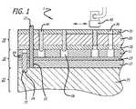
- FIG. 1is a partial cutaway side view of a fill mechanism and and an assembly of the present invention.
- FIG. 2is a top view of a standoff according to the present invention.
- an assembly 1includes a stand-off 10 comprising a double sided laminate having copper layers 11 and 12 on opposite sides of a dielectric core 13 .
- layer 11is patterned, and layer 12 is a substantially solid plane.
- Layers 11 and 12comprise tooling slots 14 , tooling pin holes 15 , and fill material receiving holes 16 that are essentially oversized holes.
- a tooling plate assembly 20includes alignment pins 21 and tooling plate 23 , and alignment pin receiving holes 24 .
- a printed wiring board (“PWB”) 30includes tooling pins 22 , holes 36 , core 33 and copper layers 31 and 32 .
- a filling mechanism/head 40is shown filling holes 36 with fill material 41 . For holes 36 already filled with fill material 41 , a portion of fill material 41 extends into holes 16 .
- FIG. 2shows an etched stand-off similar to stand-off 10 of FIG. 1 having tooling slots 14 and tooling pin holes 15 .
- Stand-off 10is preferably formed from Q-stock (double sided laminate material) having 5–10 oz. copper (layers 11 and 12 ) on both sides, or by laminating 1 ⁇ 2–12 oz. copper foil on both sides (layers 11 and 12 ) of G-10 or other substrate base material.
- Q-stockdouble sided laminate material
- Such a copper clad laminateis imaged using a modified version of art-work derived from a drill-file program of a particular PWB part number, and layer number (depending on which layers of a PWB are designated for drill).
- the holes within the patternare imaged to 0.005′′–0.100′′ per side, oversized from a stated finished diameter for each hole.
- the panelis then run through developers to form the pattern to be etched.
- the panelis then placed in an etch tank or processed through a conveyorized etcher to remove the copper from the areas not protected by the developed resist pattern on the stand-off panel, followed by stripping the resist from the panel and subsequent cleaning.
- Tooling holesare then drilled or routed into the panel before releasing it for use in the hole fill process. It should be noted that one can also plate up the copper thickness to unlimited thickness if required, and that small relief holes could be drilled using the existing drill program for each particular part number.
- Tooling plate 23can comprise any suitable supporting surface. Although the figure shows the use of pins 21 to align and affix stand-off 10 to tooling plate 23 , any suitable means may be used to align and/or couple stand-off 10 to tooling plate 23 .
- PWB 30rests on top of stand-off 10 but is only bonded to stand-off 10 by pins 22 .
- stand-off 10preferably rests on tooling plate 23 , but is only bonded to tooling plate 23 by alignment pins 21 .
- stand-off 10may be bonded, either temporarily or permanently to tooling plate 23 , and/or may be temporarily bonded to PWB 30 .
- assembly 1as comprising a printed wiring board 30
- any substantially planar device having holes to be filledcould be used in place of printed wiring board 30 as long as the device and the stand-off 10 are adapted to be coupled to and aligned with each other so as to assure proper alignment between the pattern on stand-off 10 and the pattern on the device being filled.
- Stand-off 10may be advantageously used in conjunction with a hole-fill method that includes: providing stand-off 10 ; aligning the stand-off to a tooling plate; aligning the substrate to the stand-off and placing the substrate in contact with the stand-off; and filling the plurality of holes of the substrate.
- a hole-fill methodthat includes: providing stand-off 10 ; aligning the stand-off to a tooling plate; aligning the substrate to the stand-off and placing the substrate in contact with the stand-off; and filling the plurality of holes of the substrate.
- providing an etched hole-fill stand-offcomprises forming the stand-off previously described.
- itmay be formed by imaging a copper clad laminate with an image similar to that used to image a surface of the substrate, and subjecting the imaged laminate to develop-etch-strip processing to form a pattern in a copper surface of the laminate, the pattern having a plurality of holes, each of the plurality of holes corresponding to a hole to be filled of the substrate, the laminate holes being at least slightly larger in diameter than their corresponding substrate holes.
- the foregoing methodwould typically also comprise filling the through holes of the substrate with a fill material such that the fill material extends at least partially into the holes of the stand-off, and removing the substrate from the stand-off wherein substantially all of the fill material extending into the stand-off remains after removal of the stand-off.
- An image “similar” to that used on a surface of the substrate being filledwill likely have the same pattern of through holes but with the through holes having a larger diameter than provided for in the pattern for the substrate.
Landscapes
- Engineering & Computer Science (AREA)
- Manufacturing & Machinery (AREA)
- Microelectronics & Electronic Packaging (AREA)
- Printing Elements For Providing Electric Connections Between Printed Circuits (AREA)
- Coating Apparatus (AREA)
- Manufacturing Of Printed Wiring (AREA)
- Particle Formation And Scattering Control In Inkjet Printers (AREA)
- Application Of Or Painting With Fluid Materials (AREA)
Abstract
Description
Claims (24)
Priority Applications (5)
| Application Number | Priority Date | Filing Date | Title |
|---|---|---|---|
| US10/039,942US6995321B2 (en) | 2000-05-31 | 2002-01-03 | Etched hole-fill stand-off |
| US10/201,450US6855385B2 (en) | 2000-05-31 | 2002-07-22 | PCB support plate for PCB via fill |
| AU2002357926AAU2002357926A1 (en) | 2002-01-03 | 2002-12-19 | Etched hole-fill stand-off |
| PCT/US2002/040758WO2003060954A1 (en) | 2002-01-03 | 2002-12-19 | Etched hole-fill stand-off |
| TW92100049ATW200302041A (en) | 2002-01-03 | 2003-01-02 | Etched hole-fill stand-off |
Applications Claiming Priority (3)
| Application Number | Priority Date | Filing Date | Title |
|---|---|---|---|
| US20845400P | 2000-05-31 | 2000-05-31 | |
| US09/752,629US6454154B1 (en) | 2000-05-31 | 2000-12-28 | Filling device |
| US10/039,942US6995321B2 (en) | 2000-05-31 | 2002-01-03 | Etched hole-fill stand-off |
Related Parent Applications (1)
| Application Number | Title | Priority Date | Filing Date |
|---|---|---|---|
| US09/752,629Continuation-In-PartUS6454154B1 (en) | 2000-05-31 | 2000-12-28 | Filling device |
Related Child Applications (1)
| Application Number | Title | Priority Date | Filing Date |
|---|---|---|---|
| US10/201,450Continuation-In-PartUS6855385B2 (en) | 2000-05-31 | 2002-07-22 | PCB support plate for PCB via fill |
Publications (2)
| Publication Number | Publication Date |
|---|---|
| US20020084306A1 US20020084306A1 (en) | 2002-07-04 |
| US6995321B2true US6995321B2 (en) | 2006-02-07 |
Family
ID=26903209
Family Applications (3)
| Application Number | Title | Priority Date | Filing Date |
|---|---|---|---|
| US10/026,338Expired - Fee RelatedUS6840425B2 (en) | 2000-05-31 | 2001-12-20 | Scavenging system |
| US10/026,135Expired - Fee RelatedUS6832714B2 (en) | 2000-05-31 | 2001-12-20 | Heated filling device |
| US10/039,942Expired - Fee RelatedUS6995321B2 (en) | 2000-05-31 | 2002-01-03 | Etched hole-fill stand-off |
Family Applications Before (2)
| Application Number | Title | Priority Date | Filing Date |
|---|---|---|---|
| US10/026,338Expired - Fee RelatedUS6840425B2 (en) | 2000-05-31 | 2001-12-20 | Scavenging system |
| US10/026,135Expired - Fee RelatedUS6832714B2 (en) | 2000-05-31 | 2001-12-20 | Heated filling device |
Country Status (8)
| Country | Link |
|---|---|
| US (3) | US6840425B2 (en) |
| JP (1) | JP2003535465A (en) |
| KR (1) | KR20030007755A (en) |
| CN (1) | CN1444840A (en) |
| AU (1) | AU2001264968A1 (en) |
| DE (1) | DE10196259T1 (en) |
| TW (1) | TW486782B (en) |
| WO (1) | WO2001093648A2 (en) |
Cited By (2)
| Publication number | Priority date | Publication date | Assignee | Title |
|---|---|---|---|---|
| US20090293271A1 (en)* | 2008-06-02 | 2009-12-03 | Ibiden Co., Ltd. | Printed wiring board with built-in electronic component and manufacturing method thereof |
| TWI419282B (en)* | 2009-10-05 | 2013-12-11 | Advance Materials Corp | Method for forming window bga substrate |
Families Citing this family (18)
| Publication number | Priority date | Publication date | Assignee | Title |
|---|---|---|---|---|
| JP2003535465A (en)* | 2000-05-31 | 2003-11-25 | ハネウエル・インターナシヨナル・インコーポレーテツド | Filling device |
| WO2012074563A2 (en)* | 2010-01-21 | 2012-06-07 | Henkel Corporation | Ultrasonic assisted filling of cavities |
| JP2013171862A (en)* | 2012-02-17 | 2013-09-02 | Tokyo Electron Ltd | Metal paste filling method, metal paste filling device, and via plug manufacturing method |
| DE102012216101B4 (en)* | 2012-09-12 | 2016-03-24 | Festo Ag & Co. Kg | Method for producing a coil integrated in a substrate, method for producing a multilayer printed circuit board and electronic device |
| US9878390B2 (en)* | 2013-12-05 | 2018-01-30 | Fuji Machine Mfg. Co. Ltd. | Solder supply device including a solder cup and a nozzle section with a flange section that is elastically deformable |
| CN105873709B (en)* | 2013-12-05 | 2018-09-28 | 富士机械制造株式会社 | Solder supply device |
| WO2015092877A1 (en)* | 2013-12-18 | 2015-06-25 | 富士機械製造株式会社 | Solder supply device |
| WO2015120773A1 (en) | 2014-02-13 | 2015-08-20 | Honeywell International Inc. | Compressible thermal interface materials |
| CN106132613B (en)* | 2014-03-07 | 2018-11-09 | 株式会社富士 | Solder feedway |
| US9974170B1 (en) | 2015-05-19 | 2018-05-15 | Apple Inc. | Conductive strands for fabric-based items |
| CN105499710B (en)* | 2016-01-13 | 2017-11-14 | 浙江大学台州研究院 | Scraper with complex track |
| JP6842469B2 (en) | 2016-03-08 | 2021-03-17 | ハネウェル・インターナショナル・インコーポレーテッドHoneywell International Inc. | Phase change material |
| US20170266948A1 (en)* | 2016-03-16 | 2017-09-21 | Intel Corporation | Modular squeegee head apparatus for printing materials |
| EP3431191B1 (en)* | 2016-03-18 | 2021-03-03 | Fuji Corporation | Viscous fluid supply device |
| US11041103B2 (en) | 2017-09-08 | 2021-06-22 | Honeywell International Inc. | Silicone-free thermal gel |
| US11072706B2 (en) | 2018-02-15 | 2021-07-27 | Honeywell International Inc. | Gel-type thermal interface material |
| US11373921B2 (en) | 2019-04-23 | 2022-06-28 | Honeywell International Inc. | Gel-type thermal interface material with low pre-curing viscosity and elastic properties post-curing |
| CN116217258B (en)* | 2023-01-03 | 2024-01-16 | 东阳东磁自动化科技有限公司 | Full-automatic hole filling equipment for ceramic substrate and hole filling method thereof |
Citations (81)
| Publication number | Priority date | Publication date | Assignee | Title |
|---|---|---|---|---|
| US3601523A (en) | 1970-06-19 | 1971-08-24 | Buckbee Mears Co | Through hole connectors |
| US4106187A (en) | 1975-01-18 | 1978-08-15 | The Marconi Company Limited | Curved rigid printed circuit boards |
| JPS53104857A (en) | 1977-02-25 | 1978-09-12 | Hitachi Ltd | Method of producing printed circuit board |
| JPS54139065A (en) | 1978-04-20 | 1979-10-29 | Japan Styrene Paper Corp | Resist for production of metalic through hole type printed circuit board |
| US4283243A (en) | 1978-10-24 | 1981-08-11 | E. I. Du Pont De Nemours And Company | Use of photosensitive stratum to create through-hole connections in circuit boards |
| US4360570A (en) | 1978-02-17 | 1982-11-23 | E. I. Du Pont De Nemours And Company | Use of photosensitive stratum to create through-hole connections in circuit boards |
| JPS5811172A (en) | 1981-07-14 | 1983-01-21 | Canon Inc | Inkjet head manufacturing method |
| GB2120017A (en) | 1982-05-13 | 1983-11-23 | Kollmorgen Tech Corp | Making printed circuit boards having plated through-holes |
| EP0194247A2 (en) | 1985-03-05 | 1986-09-10 | Svecia Silkscreen Maskiner AB | A screen printer adapted for providing a layer of material on the inner surface of a hole passing through a plate |
| WO1986006243A1 (en) | 1985-04-16 | 1986-10-23 | Kaspar Eidenberg | Process for the closing up of drill holes provided for in a printed circuit board |
| US4622239A (en) | 1986-02-18 | 1986-11-11 | At&T Technologies, Inc. | Method and apparatus for dispensing viscous materials |
| US4700474A (en) | 1986-11-26 | 1987-10-20 | Multitek Corporation | Apparatus and method for temporarily sealing holes in printed circuit boards |
| JPS62277794A (en) | 1986-05-27 | 1987-12-02 | 日立化成工業株式会社 | Manufacture of inner layer circuit board |
| JPS62287696A (en) | 1986-06-05 | 1987-12-14 | 日本電気株式会社 | Manufacture of multilayer printed interconnection board |
| US4777721A (en) | 1986-11-26 | 1988-10-18 | Multitek Corporation | Apparatus and method for temporarily sealing holes in printed circuit boards utilizing a thermodeformable material |
| US4783247A (en) | 1985-05-17 | 1988-11-08 | Hoechst Aktiengesellschaft | Method and manufacture for electrically insulating base material used in plated-through printed circuit panels |
| JPH01173696A (en) | 1987-12-26 | 1989-07-10 | Nissha Printing Co Ltd | Laminated circuit board |
| JPH01236694A (en) | 1988-03-17 | 1989-09-21 | Toshiba Corp | Ceramic substrate manufacturing method |
| US4884337A (en) | 1986-11-26 | 1989-12-05 | Epicor Technology, Inc. | Method for temporarily sealing holes in printed circuit boards utilizing a thermodeformable material |
| US4954313A (en) | 1989-02-03 | 1990-09-04 | Amdahl Corporation | Method and apparatus for filling high density vias |
| US4964948A (en) | 1985-04-16 | 1990-10-23 | Protocad, Inc. | Printed circuit board through hole technique |
| JPH034595A (en) | 1989-06-01 | 1991-01-10 | Tanaka Kikinzoku Kogyo Kk | Manufacturing method for printed through-hole multilayer board |
| US4995941A (en) | 1989-05-15 | 1991-02-26 | Rogers Corporation | Method of manufacture interconnect device |
| US5053921A (en) | 1989-05-15 | 1991-10-01 | Rogers Corporation | Multilayer interconnect device and method of manufacture thereof |
| US5058265A (en) | 1990-05-10 | 1991-10-22 | Rockwell International Corporation | Method for packaging a board of electronic components |
| GB2246912A (en) | 1990-07-11 | 1992-02-12 | Nippon Cmk Kk | Manufacturing printed circuit boards |
| US5117069A (en) | 1988-03-28 | 1992-05-26 | Prime Computer, Inc. | Circuit board fabrication |
| JPH04186792A (en) | 1990-11-20 | 1992-07-03 | Nec Toyama Ltd | Printed wiring board and manufacture thereof |
| US5133120A (en) | 1990-07-11 | 1992-07-28 | Nippon Cmk Corp. | Method of filling conductive material into through holes of printed wiring board |
| JPH04239193A (en) | 1991-01-14 | 1992-08-27 | Nec Corp | Filling method of via of through-hole |
| US5145691A (en) | 1990-07-18 | 1992-09-08 | Nippon Cmk Corp. | Apparatus for packing filler into through-holes or the like in a printed circuit board |
| US5191709A (en)* | 1990-08-10 | 1993-03-09 | Nippon Cmk Corp. | Method of forming through-holes in printed wiring board |
| US5220723A (en) | 1990-11-05 | 1993-06-22 | Nec Corporation | Process for preparing multi-layer printed wiring board |
| JPH05275819A (en) | 1992-01-31 | 1993-10-22 | Tatsuta Electric Wire & Cable Co Ltd | Printed wiring board |
| US5274916A (en) | 1991-12-18 | 1994-01-04 | Murata Manufacturing Co., Ltd. | Method of manufacturing ceramic multilayer electronic component |
| US5277854A (en) | 1991-06-06 | 1994-01-11 | Hunt John F | Methods and apparatus for making grids from fibers |
| US5332439A (en) | 1991-08-23 | 1994-07-26 | Hitachi Techno Engineering Co., Ltd. | Screen printing apparatus for filling through-holes in circuit board with paste |
| FR2714567A1 (en) | 1993-12-28 | 1995-06-30 | Thomson Hybrides | Through hole plating process for hybrid circuits |
| JPH07176871A (en) | 1993-12-21 | 1995-07-14 | Matsushita Electric Ind Co Ltd | Method for manufacturing resin multilayer substrate |
| US5451721A (en) | 1990-09-27 | 1995-09-19 | International Business Machines Corporation | Multilayer printed circuit board and method for fabricating same |
| US5456004A (en) | 1994-01-04 | 1995-10-10 | Dell Usa, L.P. | Anisotropic interconnect methodology for cost effective manufacture of high density printed circuit boards |
| US5471091A (en) | 1991-06-06 | 1995-11-28 | Lsi Logic Corporation | Techniques for via formation and filling |
| EP0713358A2 (en) | 1994-11-21 | 1996-05-22 | International Business Machines Corporation | Circuit board |
| US5532516A (en) | 1991-08-26 | 1996-07-02 | Lsi Logic Corportion | Techniques for via formation and filling |
| JPH08172265A (en) | 1994-12-20 | 1996-07-02 | Fuji Elelctrochem Co Ltd | Method for forming conductive electrode on ceramic sheet |
| JPH08191184A (en) | 1995-01-11 | 1996-07-23 | Matsushita Electric Ind Co Ltd | Method and apparatus for manufacturing printed wiring board |
| EP0723388A1 (en) | 1995-01-20 | 1996-07-24 | Matsushita Electric Industrial Co., Ltd | Printed circuit board |
| US5540779A (en) | 1992-04-09 | 1996-07-30 | International Business Machines Corporation | Apparatus for manufacture of multi-layer ceramic interconnect structures |
| US5591353A (en) | 1994-08-18 | 1997-01-07 | Texas Instruments Incorporated | Reduction of surface copper thickness on surface mount printed wire boards with copper plated through holes by the chemical planarization method |
| US5610103A (en) | 1995-12-12 | 1997-03-11 | Applied Materials, Inc. | Ultrasonic wave assisted contact hole filling |
| JPH0983135A (en) | 1995-09-18 | 1997-03-28 | Matsushita Electric Ind Co Ltd | Through-hole board manufacturing equipment |
| US5637834A (en) | 1995-02-03 | 1997-06-10 | Motorola, Inc. | Multilayer circuit substrate and method for forming same |
| US5662987A (en) | 1995-02-17 | 1997-09-02 | International Business Machines Corporation | Multilayer printed wiring board and method of making same |
| JPH09321399A (en) | 1996-05-29 | 1997-12-12 | Matsushita Electric Ind Co Ltd | Printed wiring board and method of manufacturing the same |
| US5699613A (en) | 1995-09-25 | 1997-12-23 | International Business Machines Corporation | Fine dimension stacked vias for a multiple layer circuit board structure |
| US5707575A (en) | 1994-07-28 | 1998-01-13 | Micro Substrates Corporation | Method for filling vias in ceramic substrates with composite metallic paste |
| JPH1065339A (en) | 1996-08-22 | 1998-03-06 | Sony Corp | Multilayer printed wiring board and method manufacturing therfor |
| US5744285A (en) | 1996-07-18 | 1998-04-28 | E. I. Du Pont De Nemours And Company | Composition and process for filling vias |
| US5744171A (en) | 1993-09-15 | 1998-04-28 | Lsi Logic Corporation | System for fabricating conductive epoxy grid array semiconductor packages |
| US5753976A (en) | 1996-06-14 | 1998-05-19 | Minnesota Mining And Manufacturing Company | Multi-layer circuit having a via matrix interlayer connection |
| US5761803A (en) | 1996-06-26 | 1998-06-09 | St. John; Frank | Method of forming plugs in vias of a circuit board by utilizing a porous membrane |
| US5766670A (en) | 1993-11-17 | 1998-06-16 | Ibm | Via fill compositions for direct attach of devices and methods for applying same |
| JPH10256687A (en) | 1997-03-14 | 1998-09-25 | Matsushita Electric Ind Co Ltd | Conductor paste composition for filling via holes and printed wiring board using the same |
| US5822856A (en) | 1996-06-28 | 1998-10-20 | International Business Machines Corporation | Manufacturing circuit board assemblies having filled vias |
| US5824155A (en) | 1995-11-08 | 1998-10-20 | Ford Motor Company | Method and apparatus for dispensing viscous material |
| US5906042A (en) | 1995-10-04 | 1999-05-25 | Prolinx Labs Corporation | Method and structure to interconnect traces of two conductive layers in a printed circuit board |
| US5925414A (en) | 1996-11-20 | 1999-07-20 | International Business Corpration | Nozzle and method for extruding conductive paste into high aspect ratio openings |
| US5985185A (en)* | 1994-10-19 | 1999-11-16 | Telefonaktiebolaget Lm Ericsson | Optocomponent capsule having an optical interface |
| US5994779A (en) | 1997-05-02 | 1999-11-30 | Advanced Micro Devices, Inc. | Semiconductor fabrication employing a spacer metallization technique |
| US6009620A (en) | 1998-07-15 | 2000-01-04 | International Business Machines Corporation | Method of making a printed circuit board having filled holes |
| US6015520A (en) | 1997-05-15 | 2000-01-18 | International Business Machines Corporation | Method for filling holes in printed wiring boards |
| WO2000013474A1 (en) | 1998-09-02 | 2000-03-09 | Hadco Santa Clara, Inc. | Forming plugs in vias of circuit board layers and subassemblies |
| GB2341347A (en) | 1998-09-10 | 2000-03-15 | Crossflow Int Ltd | A method and apparatus for applying a viscous or paste material onto a substrate |
| US6079100A (en) | 1998-05-12 | 2000-06-27 | International Business Machines Corporation | Method of making a printed circuit board having filled holes and fill member for use therewith |
| US6090474A (en)* | 1998-09-01 | 2000-07-18 | International Business Machines Corporation | Flowable compositions and use in filling vias and plated through-holes |
| US6098282A (en)* | 1994-11-21 | 2000-08-08 | International Business Machines Corporation | Laminar stackable circuit board structure with capacitor |
| US6149857A (en) | 1995-08-01 | 2000-11-21 | Loctite (R&D) Limited | Method of making films and coatings having anisotropic conductive pathways therein |
| US6184133B1 (en) | 1994-04-28 | 2001-02-06 | Fujitsu Limited | Method of forming an assembly board with insulator filled through holes |
| US6261501B1 (en) | 1998-01-23 | 2001-07-17 | Apic Yamada Corporation | Resin sealing method for a semiconductor device |
| US6281448B1 (en) | 1996-12-26 | 2001-08-28 | Matsushita Electric Industrial Co., Ltd. | Printed circuit board and electronic components |
| US20030215568A1 (en)* | 2000-08-31 | 2003-11-20 | Micron Technology, Inc. | Method for filling a wafer through-via with a conductive material |
Family Cites Families (29)
| Publication number | Priority date | Publication date | Assignee | Title |
|---|---|---|---|---|
| JPS5210487A (en) | 1975-07-09 | 1977-01-26 | Nippon Soda Co Ltd | Production of gluconic acid or salts thereof by fermentation |
| JPS5928260B2 (en) | 1976-07-15 | 1984-07-11 | 松下電器産業株式会社 | Ultrasonic probe position detection method and device |
| JPS54139006A (en) | 1978-04-20 | 1979-10-29 | Toshiba Corp | Stator for rotary electric machine |
| US4498275A (en) | 1979-04-16 | 1985-02-12 | Lykes Pasco Packing Company | Rotary filling and capping apparatus |
| US4549387A (en)* | 1982-07-07 | 1985-10-29 | Aci Australia Limited | Flexible container filling apparatus |
| US4664308A (en)* | 1985-10-30 | 1987-05-12 | Hollis Automation, Inc. | Mass soldering system providing an oscillating air blast |
| US4696096A (en)* | 1986-02-21 | 1987-09-29 | Micro Electronic Systems, Inc. | Reworking methods and apparatus for surface mounted technology circuit boards |
| JPS63295057A (en)* | 1987-05-27 | 1988-12-01 | Hitachi Ltd | Solder coating equipment |
| ES2082768T3 (en) | 1988-06-08 | 1996-04-01 | Philips Electronics Nv | SYNCHRONISM DEMODULATOR. |
| US5066216A (en)* | 1989-09-22 | 1991-11-19 | Binney & Smith Inc. | Apparatus for injection of viscous material |
| DD296375B5 (en)* | 1990-06-28 | 1994-02-17 | Thaelmann Schwermaschbau Veb | DEVICE FOR REALIZING THE LONGITUDINAL WATER LEAKAGE OF REMOTE CABLES BUILT ON PLASTISOLATED VEINS |
| EP0506403B1 (en)* | 1991-03-25 | 1995-08-23 | Tektronix, Inc. | Method and apparatus for providing phase change ink to an ink jet printer |
| FR2684836B3 (en) | 1991-12-04 | 1994-03-18 | Assistance Prod Envi Lab | METHOD FOR MANUFACTURING PRINTED CIRCUIT BOARDS WITH VIA HOLES. |
| US5249436A (en)* | 1992-04-09 | 1993-10-05 | Indugas, Inc. | Simplified, low cost absorption heat pump |
| JP2963843B2 (en)* | 1994-06-06 | 1999-10-18 | 株式会社ミツバ | Washer nozzle for vehicles |
| US5622216A (en) | 1994-11-22 | 1997-04-22 | Brown; Stuart B. | Method and apparatus for metal solid freeform fabrication utilizing partially solidified metal slurry |
| JP3431729B2 (en)* | 1995-07-12 | 2003-07-28 | 松下電器産業株式会社 | Circuit board manufacturing method and manufacturing apparatus |
| US5678752A (en)* | 1995-08-01 | 1997-10-21 | International Business Machines Corporation | Wave soldering process |
| GB9523555D0 (en)* | 1995-11-17 | 1996-01-17 | Cambridge Consultants | Filling containers with particulate material |
| JP3410639B2 (en)* | 1997-07-23 | 2003-05-26 | 株式会社日立製作所 | Paste filling method, soldering method and paste printing machine |
| JPH1154909A (en)* | 1997-08-04 | 1999-02-26 | Tdk Corp | Method and apparatus for charging paste for through-holes |
| US6281488B1 (en)* | 1998-12-09 | 2001-08-28 | Sandia Corporation | Fiber optic coupled optical sensor |
| JP4110663B2 (en)* | 1999-04-13 | 2008-07-02 | 旭硝子株式会社 | Vacuum degassing method for molten glass flow |
| JP2000318711A (en)* | 1999-05-12 | 2000-11-21 | Kao Corp | Liquid filling method |
| US6491204B1 (en)* | 1999-11-30 | 2002-12-10 | Gunter Erdmann | Stencil wiping device |
| JP2003535465A (en)* | 2000-05-31 | 2003-11-25 | ハネウエル・インターナシヨナル・インコーポレーテツド | Filling device |
| US6454154B1 (en)* | 2000-05-31 | 2002-09-24 | Honeywell Advanced Circuits, Inc. | Filling device |
| DE10196262T1 (en)* | 2000-05-31 | 2003-05-15 | Honeywell Int Inc | filling system |
| US6638363B2 (en)* | 2000-11-22 | 2003-10-28 | Gunter Erdmann | Method of cleaning solder paste |
- 2001
- 2001-05-24JPJP2001588300Apatent/JP2003535465A/ennot_activeWithdrawn
- 2001-05-24WOPCT/US2001/016986patent/WO2001093648A2/enactiveApplication Filing
- 2001-05-24CNCN01813666Apatent/CN1444840A/enactivePending
- 2001-05-24KRKR1020027016198Apatent/KR20030007755A/ennot_activeWithdrawn
- 2001-05-24AUAU2001264968Apatent/AU2001264968A1/ennot_activeAbandoned
- 2001-05-24DEDE10196259Tpatent/DE10196259T1/ennot_activeWithdrawn
- 2001-08-28TWTW090113057Apatent/TW486782B/enactive
- 2001-12-20USUS10/026,338patent/US6840425B2/ennot_activeExpired - Fee Related
- 2001-12-20USUS10/026,135patent/US6832714B2/ennot_activeExpired - Fee Related
- 2002
- 2002-01-03USUS10/039,942patent/US6995321B2/ennot_activeExpired - Fee Related
Patent Citations (90)
| Publication number | Priority date | Publication date | Assignee | Title |
|---|---|---|---|---|
| US3601523A (en) | 1970-06-19 | 1971-08-24 | Buckbee Mears Co | Through hole connectors |
| US4106187A (en) | 1975-01-18 | 1978-08-15 | The Marconi Company Limited | Curved rigid printed circuit boards |
| JPS53104857A (en) | 1977-02-25 | 1978-09-12 | Hitachi Ltd | Method of producing printed circuit board |
| US4360570A (en) | 1978-02-17 | 1982-11-23 | E. I. Du Pont De Nemours And Company | Use of photosensitive stratum to create through-hole connections in circuit boards |
| JPS54139065A (en) | 1978-04-20 | 1979-10-29 | Japan Styrene Paper Corp | Resist for production of metalic through hole type printed circuit board |
| US4283243A (en) | 1978-10-24 | 1981-08-11 | E. I. Du Pont De Nemours And Company | Use of photosensitive stratum to create through-hole connections in circuit boards |
| JPS5811172A (en) | 1981-07-14 | 1983-01-21 | Canon Inc | Inkjet head manufacturing method |
| GB2120017A (en) | 1982-05-13 | 1983-11-23 | Kollmorgen Tech Corp | Making printed circuit boards having plated through-holes |
| EP0194247A2 (en) | 1985-03-05 | 1986-09-10 | Svecia Silkscreen Maskiner AB | A screen printer adapted for providing a layer of material on the inner surface of a hole passing through a plate |
| WO1986006243A1 (en) | 1985-04-16 | 1986-10-23 | Kaspar Eidenberg | Process for the closing up of drill holes provided for in a printed circuit board |
| US4964948A (en) | 1985-04-16 | 1990-10-23 | Protocad, Inc. | Printed circuit board through hole technique |
| US4783247A (en) | 1985-05-17 | 1988-11-08 | Hoechst Aktiengesellschaft | Method and manufacture for electrically insulating base material used in plated-through printed circuit panels |
| US4622239A (en) | 1986-02-18 | 1986-11-11 | At&T Technologies, Inc. | Method and apparatus for dispensing viscous materials |
| JPS62277794A (en) | 1986-05-27 | 1987-12-02 | 日立化成工業株式会社 | Manufacture of inner layer circuit board |
| JPS62287696A (en) | 1986-06-05 | 1987-12-14 | 日本電気株式会社 | Manufacture of multilayer printed interconnection board |
| US4777721A (en) | 1986-11-26 | 1988-10-18 | Multitek Corporation | Apparatus and method for temporarily sealing holes in printed circuit boards utilizing a thermodeformable material |
| US4884337A (en) | 1986-11-26 | 1989-12-05 | Epicor Technology, Inc. | Method for temporarily sealing holes in printed circuit boards utilizing a thermodeformable material |
| US4700474A (en) | 1986-11-26 | 1987-10-20 | Multitek Corporation | Apparatus and method for temporarily sealing holes in printed circuit boards |
| JPH01173696A (en) | 1987-12-26 | 1989-07-10 | Nissha Printing Co Ltd | Laminated circuit board |
| JPH01236694A (en) | 1988-03-17 | 1989-09-21 | Toshiba Corp | Ceramic substrate manufacturing method |
| US5117069A (en) | 1988-03-28 | 1992-05-26 | Prime Computer, Inc. | Circuit board fabrication |
| US4954313A (en) | 1989-02-03 | 1990-09-04 | Amdahl Corporation | Method and apparatus for filling high density vias |
| US4995941A (en) | 1989-05-15 | 1991-02-26 | Rogers Corporation | Method of manufacture interconnect device |
| US5053921A (en) | 1989-05-15 | 1991-10-01 | Rogers Corporation | Multilayer interconnect device and method of manufacture thereof |
| JPH034595A (en) | 1989-06-01 | 1991-01-10 | Tanaka Kikinzoku Kogyo Kk | Manufacturing method for printed through-hole multilayer board |
| US5058265A (en) | 1990-05-10 | 1991-10-22 | Rockwell International Corporation | Method for packaging a board of electronic components |
| GB2246912A (en) | 1990-07-11 | 1992-02-12 | Nippon Cmk Kk | Manufacturing printed circuit boards |
| US5133120A (en) | 1990-07-11 | 1992-07-28 | Nippon Cmk Corp. | Method of filling conductive material into through holes of printed wiring board |
| US5145691A (en) | 1990-07-18 | 1992-09-08 | Nippon Cmk Corp. | Apparatus for packing filler into through-holes or the like in a printed circuit board |
| US5191709A (en)* | 1990-08-10 | 1993-03-09 | Nippon Cmk Corp. | Method of forming through-holes in printed wiring board |
| US5451721A (en) | 1990-09-27 | 1995-09-19 | International Business Machines Corporation | Multilayer printed circuit board and method for fabricating same |
| US5220723A (en) | 1990-11-05 | 1993-06-22 | Nec Corporation | Process for preparing multi-layer printed wiring board |
| JPH04186792A (en) | 1990-11-20 | 1992-07-03 | Nec Toyama Ltd | Printed wiring board and manufacture thereof |
| JPH04239193A (en) | 1991-01-14 | 1992-08-27 | Nec Corp | Filling method of via of through-hole |
| US5277854A (en) | 1991-06-06 | 1994-01-11 | Hunt John F | Methods and apparatus for making grids from fibers |
| US5471091A (en) | 1991-06-06 | 1995-11-28 | Lsi Logic Corporation | Techniques for via formation and filling |
| US5332439A (en) | 1991-08-23 | 1994-07-26 | Hitachi Techno Engineering Co., Ltd. | Screen printing apparatus for filling through-holes in circuit board with paste |
| US5532516A (en) | 1991-08-26 | 1996-07-02 | Lsi Logic Corportion | Techniques for via formation and filling |
| US5274916A (en) | 1991-12-18 | 1994-01-04 | Murata Manufacturing Co., Ltd. | Method of manufacturing ceramic multilayer electronic component |
| JPH05275819A (en) | 1992-01-31 | 1993-10-22 | Tatsuta Electric Wire & Cable Co Ltd | Printed wiring board |
| US5540779A (en) | 1992-04-09 | 1996-07-30 | International Business Machines Corporation | Apparatus for manufacture of multi-layer ceramic interconnect structures |
| US5578151A (en) | 1992-04-09 | 1996-11-26 | International Business Machines Corporation | Manufacture of a multi-layer interconnect structure |
| US5744171A (en) | 1993-09-15 | 1998-04-28 | Lsi Logic Corporation | System for fabricating conductive epoxy grid array semiconductor packages |
| US6106891A (en) | 1993-11-17 | 2000-08-22 | International Business Machines Corporation | Via fill compositions for direct attach of devices and method for applying same |
| US5766670A (en) | 1993-11-17 | 1998-06-16 | Ibm | Via fill compositions for direct attach of devices and methods for applying same |
| US6134772A (en)* | 1993-11-17 | 2000-10-24 | International Business Machines Corporation | Via fill compositions for direct attach of devices and methods of applying same |
| JPH07176871A (en) | 1993-12-21 | 1995-07-14 | Matsushita Electric Ind Co Ltd | Method for manufacturing resin multilayer substrate |
| FR2714567A1 (en) | 1993-12-28 | 1995-06-30 | Thomson Hybrides | Through hole plating process for hybrid circuits |
| US5456004A (en) | 1994-01-04 | 1995-10-10 | Dell Usa, L.P. | Anisotropic interconnect methodology for cost effective manufacture of high density printed circuit boards |
| US6184133B1 (en) | 1994-04-28 | 2001-02-06 | Fujitsu Limited | Method of forming an assembly board with insulator filled through holes |
| US5707575A (en) | 1994-07-28 | 1998-01-13 | Micro Substrates Corporation | Method for filling vias in ceramic substrates with composite metallic paste |
| US5591353A (en) | 1994-08-18 | 1997-01-07 | Texas Instruments Incorporated | Reduction of surface copper thickness on surface mount printed wire boards with copper plated through holes by the chemical planarization method |
| US5985185A (en)* | 1994-10-19 | 1999-11-16 | Telefonaktiebolaget Lm Ericsson | Optocomponent capsule having an optical interface |
| US6098282A (en)* | 1994-11-21 | 2000-08-08 | International Business Machines Corporation | Laminar stackable circuit board structure with capacitor |
| EP0713358A2 (en) | 1994-11-21 | 1996-05-22 | International Business Machines Corporation | Circuit board |
| JPH08172265A (en) | 1994-12-20 | 1996-07-02 | Fuji Elelctrochem Co Ltd | Method for forming conductive electrode on ceramic sheet |
| JPH08191184A (en) | 1995-01-11 | 1996-07-23 | Matsushita Electric Ind Co Ltd | Method and apparatus for manufacturing printed wiring board |
| EP0723388A1 (en) | 1995-01-20 | 1996-07-24 | Matsushita Electric Industrial Co., Ltd | Printed circuit board |
| US5637834A (en) | 1995-02-03 | 1997-06-10 | Motorola, Inc. | Multilayer circuit substrate and method for forming same |
| US5662987A (en) | 1995-02-17 | 1997-09-02 | International Business Machines Corporation | Multilayer printed wiring board and method of making same |
| US6149857A (en) | 1995-08-01 | 2000-11-21 | Loctite (R&D) Limited | Method of making films and coatings having anisotropic conductive pathways therein |
| JPH0983135A (en) | 1995-09-18 | 1997-03-28 | Matsushita Electric Ind Co Ltd | Through-hole board manufacturing equipment |
| US5699613A (en) | 1995-09-25 | 1997-12-23 | International Business Machines Corporation | Fine dimension stacked vias for a multiple layer circuit board structure |
| US5906042A (en) | 1995-10-04 | 1999-05-25 | Prolinx Labs Corporation | Method and structure to interconnect traces of two conductive layers in a printed circuit board |
| US5824155A (en) | 1995-11-08 | 1998-10-20 | Ford Motor Company | Method and apparatus for dispensing viscous material |
| US5851344A (en) | 1995-12-12 | 1998-12-22 | Applied Materials, Inc. | Ultrasonic wave assisted contact hole filling |
| US5610103A (en) | 1995-12-12 | 1997-03-11 | Applied Materials, Inc. | Ultrasonic wave assisted contact hole filling |
| JPH09321399A (en) | 1996-05-29 | 1997-12-12 | Matsushita Electric Ind Co Ltd | Printed wiring board and method of manufacturing the same |
| US5753976A (en) | 1996-06-14 | 1998-05-19 | Minnesota Mining And Manufacturing Company | Multi-layer circuit having a via matrix interlayer connection |
| US6153508A (en) | 1996-06-14 | 2000-11-28 | 3M Innovative Properties Company | Multi-layer circuit having a via matrix interlayer connection and method for fabricating the same |
| US5761803A (en) | 1996-06-26 | 1998-06-09 | St. John; Frank | Method of forming plugs in vias of a circuit board by utilizing a porous membrane |
| US5822856A (en) | 1996-06-28 | 1998-10-20 | International Business Machines Corporation | Manufacturing circuit board assemblies having filled vias |
| US6000129A (en) | 1996-06-28 | 1999-12-14 | International Business Machines Corporation | Process for manufacturing a circuit with filled holes |
| US6138350A (en) | 1996-06-28 | 2000-10-31 | International Business Machines Corporation | Process for manufacturing a circuit board with filled holes |
| US5744285A (en) | 1996-07-18 | 1998-04-28 | E. I. Du Pont De Nemours And Company | Composition and process for filling vias |
| JPH1065339A (en) | 1996-08-22 | 1998-03-06 | Sony Corp | Multilayer printed wiring board and method manufacturing therfor |
| US5925414A (en) | 1996-11-20 | 1999-07-20 | International Business Corpration | Nozzle and method for extruding conductive paste into high aspect ratio openings |
| US6281448B1 (en) | 1996-12-26 | 2001-08-28 | Matsushita Electric Industrial Co., Ltd. | Printed circuit board and electronic components |
| JPH10256687A (en) | 1997-03-14 | 1998-09-25 | Matsushita Electric Ind Co Ltd | Conductor paste composition for filling via holes and printed wiring board using the same |
| US5994779A (en) | 1997-05-02 | 1999-11-30 | Advanced Micro Devices, Inc. | Semiconductor fabrication employing a spacer metallization technique |
| US6015520A (en) | 1997-05-15 | 2000-01-18 | International Business Machines Corporation | Method for filling holes in printed wiring boards |
| US6261501B1 (en) | 1998-01-23 | 2001-07-17 | Apic Yamada Corporation | Resin sealing method for a semiconductor device |
| US6079100A (en) | 1998-05-12 | 2000-06-27 | International Business Machines Corporation | Method of making a printed circuit board having filled holes and fill member for use therewith |
| US6009620A (en) | 1998-07-15 | 2000-01-04 | International Business Machines Corporation | Method of making a printed circuit board having filled holes |
| US6090474A (en)* | 1998-09-01 | 2000-07-18 | International Business Machines Corporation | Flowable compositions and use in filling vias and plated through-holes |
| WO2000013474A1 (en) | 1998-09-02 | 2000-03-09 | Hadco Santa Clara, Inc. | Forming plugs in vias of circuit board layers and subassemblies |
| US6276055B1 (en) | 1998-09-02 | 2001-08-21 | Hadco Santa Clara, Inc. | Method and apparatus for forming plugs in vias of a circuit board layer |
| US6282782B1 (en)* | 1998-09-02 | 2001-09-04 | Hadco Santa Clara, Inc. | Forming plugs in vias of circuit board layers and subassemblies |
| GB2341347A (en) | 1998-09-10 | 2000-03-15 | Crossflow Int Ltd | A method and apparatus for applying a viscous or paste material onto a substrate |
| US20030215568A1 (en)* | 2000-08-31 | 2003-11-20 | Micron Technology, Inc. | Method for filling a wafer through-via with a conductive material |
Non-Patent Citations (3)
| Title |
|---|
| Multilayer Printed Circuit Board Connections, Apr. 1996. |
| Process for Forming Copper Clad Vias, Aug. 1989. |
| Via Etching Process, Feb. 1972. |
Cited By (3)
| Publication number | Priority date | Publication date | Assignee | Title |
|---|---|---|---|---|
| US20090293271A1 (en)* | 2008-06-02 | 2009-12-03 | Ibiden Co., Ltd. | Printed wiring board with built-in electronic component and manufacturing method thereof |
| US8291584B2 (en)* | 2008-06-02 | 2012-10-23 | Ibiden Co., Ltd. | Method of manufacturing a printed wiring board with built-in electronic component |
| TWI419282B (en)* | 2009-10-05 | 2013-12-11 | Advance Materials Corp | Method for forming window bga substrate |
Also Published As
| Publication number | Publication date |
|---|---|
| DE10196259T1 (en) | 2003-05-15 |
| US20020084305A1 (en) | 2002-07-04 |
| KR20030007755A (en) | 2003-01-23 |
| WO2001093648A2 (en) | 2001-12-06 |
| TW486782B (en) | 2002-05-11 |
| US6832714B2 (en) | 2004-12-21 |
| US6840425B2 (en) | 2005-01-11 |
| CN1444840A (en) | 2003-09-24 |
| WO2001093648A3 (en) | 2002-05-23 |
| JP2003535465A (en) | 2003-11-25 |
| US20020088840A1 (en) | 2002-07-11 |
| AU2001264968A1 (en) | 2001-12-11 |
| US20020084306A1 (en) | 2002-07-04 |
Similar Documents
| Publication | Publication Date | Title |
|---|---|---|
| US6995321B2 (en) | Etched hole-fill stand-off | |
| US6005198A (en) | Wiring board constructions and methods of making same | |
| US4965702A (en) | Chip carrier package and method of manufacture | |
| US7281328B2 (en) | Method of fabricating rigid-flexible printed circuit board | |
| US20040118605A1 (en) | Circuit board having a multi-functional hole | |
| US20060180346A1 (en) | High aspect ratio plated through holes in a printed circuit board | |
| US20070070613A1 (en) | Method of manufacturing high density printed circuit boad | |
| US20130243995A1 (en) | Carrier For Manufacturing Substrate and Method Of Manufacturing Substrate Using The Same | |
| US20070062730A1 (en) | Controlled depth etched vias | |
| US6921505B2 (en) | Hole filling using an etched hole-fill stand-off | |
| US20120199388A1 (en) | Printed circuit board and manufacturing method thereof | |
| EP0144943A2 (en) | Process using plasma for forming conductive through-holes through a dielectric layer | |
| JP2010087168A (en) | Method for manufacturing multilayer printed circuit board | |
| EP1802187A2 (en) | Printed circuit board and manufacturing method thereof | |
| JP2003046243A (en) | Method for manufacturing high-density multilayer build-up wiring board | |
| US20110005071A1 (en) | Printed Circuit Board and Manufacturing Method Thereof | |
| JPH11195849A (en) | Flexible printed wiring board and its manufacturing method | |
| WO2003060954A1 (en) | Etched hole-fill stand-off | |
| JP4659604B2 (en) | Positioning device for conveying jig for component mounting of flexible printed wiring board | |
| GB2247361A (en) | Conductive through-holes in printed wiring boards | |
| KR101055455B1 (en) | Carrier member for substrate manufacturing and method for manufacturing substrate using same | |
| KR101077377B1 (en) | A carrier member for manufacturing a substrate and a method of manufacturing a substrate using the same | |
| US6391211B1 (en) | Method for making an electrical circuit board | |
| KR102751555B1 (en) | Method of manufacturing printed circuit board with fine pitch | |
| JP4395959B2 (en) | Method for manufacturing printed wiring board |
Legal Events
| Date | Code | Title | Description |
|---|---|---|---|
| AS | Assignment | Owner name:TTM ADVANCED CIRCUITS, INC., WISCONSIN Free format text:CHANGE OF NAME;ASSIGNOR:HONEYWELL ADVANCED CIRCUITS, INC.;REEL/FRAME:013993/0272 Effective date:20030317 | |
| AS | Assignment | Owner name:HONEYWELL ADVANCED CIRCUITS, MINNESOTA Free format text:ASSIGNMENT OF ASSIGNORS INTEREST;ASSIGNORS:LEE, BRUCE W.;PEDIGO, JESSE L.;REEL/FRAME:016704/0380;SIGNING DATES FROM 20020108 TO 20020109 | |
| AS | Assignment | Owner name:WACHOVIA BANK, NATIONAL ASSOCIATION, AS ADMINISTRA Free format text:NOTICE OF GRANT OF SECURITY INTEREST;ASSIGNOR:TTM ADVANCED CIRCUITS, INC.;REEL/FRAME:016522/0813 Effective date:20050715 | |
| CC | Certificate of correction | ||
| AS | Assignment | Owner name:TTM ADVANCED CIRCUITS, INC., WISCONSIN Free format text:TERMINATION OF SECURITY INTEREST IN PATENTS (RELEASES R/F;ASSIGNOR:WACHOVIA BANK, NATIONAL ASSOCIATION;REEL/FRAME:018442/0589 Effective date:20061027 Owner name:UBS AG, STAMFORD BRANCH, CONNECTICUT Free format text:PATENT SECURITY AGREEMENT;ASSIGNOR:TTM ADVANCED CIRCUITS, INC.;REEL/FRAME:018442/0594 Effective date:20061027 | |
| AS | Assignment | Owner name:TTM ADVANCED CIRCUITS, INC., WISCONSIN Free format text:RELEASE OF SECURITY AGREEMENT;ASSIGNOR:UBS AG, STAMFORD BRANCH;REEL/FRAME:021266/0276 Effective date:20080514 | |
| REMI | Maintenance fee reminder mailed | ||
| LAPS | Lapse for failure to pay maintenance fees | ||
| STCH | Information on status: patent discontinuation | Free format text:PATENT EXPIRED DUE TO NONPAYMENT OF MAINTENANCE FEES UNDER 37 CFR 1.362 | |
| FP | Lapsed due to failure to pay maintenance fee | Effective date:20100207 |