US6995068B1 - Double-implant high performance varactor and method for manufacturing same - Google Patents
Double-implant high performance varactor and method for manufacturing sameDownload PDFInfo
- Publication number
- US6995068B1 US6995068B1US09/590,462US59046200AUS6995068B1US 6995068 B1US6995068 B1US 6995068B1US 59046200 AUS59046200 AUS 59046200AUS 6995068 B1US6995068 B1US 6995068B1
- Authority
- US
- United States
- Prior art keywords
- implant
- dopant concentration
- epitaxial layer
- conductivity type
- forming
- Prior art date
- Legal status (The legal status is an assumption and is not a legal conclusion. Google has not performed a legal analysis and makes no representation as to the accuracy of the status listed.)
- Expired - Lifetime, expires
Links
Images


Classifications
- H—ELECTRICITY
- H10—SEMICONDUCTOR DEVICES; ELECTRIC SOLID-STATE DEVICES NOT OTHERWISE PROVIDED FOR
- H10D—INORGANIC ELECTRIC SEMICONDUCTOR DEVICES
- H10D1/00—Resistors, capacitors or inductors
- H10D1/01—Manufacture or treatment
- H10D1/045—Manufacture or treatment of capacitors having potential barriers, e.g. varactors
- H—ELECTRICITY
- H10—SEMICONDUCTOR DEVICES; ELECTRIC SOLID-STATE DEVICES NOT OTHERWISE PROVIDED FOR
- H10D—INORGANIC ELECTRIC SEMICONDUCTOR DEVICES
- H10D1/00—Resistors, capacitors or inductors
- H10D1/60—Capacitors
- H10D1/62—Capacitors having potential barriers
- H10D1/64—Variable-capacitance diodes, e.g. varactors
Definitions
- This inventionrelates generally to a method for fabricating a varactor diode on a semiconductor substrate. More particularly, the present invention relates to a method for fabricating high quality factor (Q), high tuning range diodes having a double base implant.
- Qquality factor
- Varactor diodesare commonly used as tuning elements in oscillators, as multiplication elements in harmonic generators or multipliers, and as impedance control elements in analog and digital phase shifters at radio microwave or millimeter wave frequencies.
- Varactor diodesare semiconductor devices also known as variable-capacitance diodes or voltage variable capacitors.
- the capacitanceis not constant, but rather varies with the voltage applied to the device. The larger the reverse voltage applied to the diode, the larger the space charge width within the diode and the smaller the capacitance.
- impedance control elements in variable phase shiftersthe voltage is varied to change the capacitance of the diode and hence the impedance thereby effecting a phase shift change.
- a conventional varactor diodeincorporates an active semiconductor layer that is sandwiched between a pair of contact layers.
- the two contact layersare of high conductivity and are of opposite conductivity type from each other, such that one of the contact layers forms a P-N junction with the active layer.
- the thickness of the active layer, as well as the relative conductivity between the active layer and each of the contact layers,determines the operating characteristics of the varactor.
- Varactor diodesare frequently fabricated by initially providing a silicon substrate having a resistivity that matches that of the desired active layer. The heavily doped contact layers are then epitaxially formed and conductor material is deposited on the contact layers. Alternatively, the diode can be formed by starting with a high conductivity substrate and then sequentially forming an epitaxial active layer and epitaxial contact layer.
- a common practiceutilizes the emitter-base junction of an NPN transistor as a varactor. This practice, however, typically creates a varactor having relatively high leakage current and relatively low capacitance sensitivity. The high base resistance of such a structure also may lead to a low value for Q, or quality factor, which is unfavorable for radio frequency (RF) applications.
- RFradio frequency
- Known varactor systemsemploy a single implant. This is because current double-implant processes do not provide a method for creating varactors having high capacitance density, high capacitance tuning range, low leakage current, and high Q values.
- the present inventionachieves an advance in the art by providing a method and structure for a new varactor design that meets the above challenges.
- high tuning rangemay be maintained by utilizing a shallow implant that exhibits a steep implant profile, but high series resistance and/or high leakage current may be experienced.
- a varactor formed using a single, shallow implanttypically will be characterized by high voltage sensitivity, but low Q and/or high leakage current.
- a varactor made in accordance with the present inventionutilizes the base-emitter junction of a specially optimized varactor formed with a double base implant.
- a first, shallow base implantoptimizes capacitance, leakage current, and tuning range.
- a second, deeper base implantis used to improve Q by reducing the base resistance.
- the varactorpreferably includes a third terminal (e.g., a collector terminal), which isolates the emitter-base junction from the substrate, providing flexibility in circuit applications.
- FIGS. 1 through 14illustrate an exemplary process sequence for forming a varactor device on a semiconductor substrate in accordance with one embodiment of the present invention
- FIG. 15illustrates empirically a simulated as-implanted dopant concentration profile for a varactor formed in accordance with one embodiment of the present invention
- FIG. 16illustrates another aspect of the simulated as-implanted dopant concentration profile for a varactor formed in accordance with one embodiment of the present invention.
- FIG. 17is a flow diagram depicting a method for forming a varactor device on a semiconductor substrate in accordance with one embodiment of the present invention.
- BiCMOSbipolar complementary metal oxide silicon
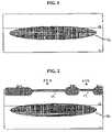
- FIGS. 1 through 9generally illustrate the formation of a so-called isolation structure of a varactor device on a semiconductor substrate.
- the isolation structurepreferably defines an implant region 81 (see FIG. 8 ) wherein a double-implant varactor device in accordance with the present invention may be formed.
- a semiconductor substrate 11comprising a suitable semiconductor material is provided.
- substrate 11comprises single-crystal silicon of a P-type conductivity and has a resistivity on the order of about 6 to 8 ohm-centimeters.
- a screen oxide layer(not shown) is formed on substrate 11 .
- the screen oxide layeris thermally grown and has a thickness on the order of about 200 to 300 angstroms. The screen oxide layer serves to protect the surface of substrate 11 from contamination during implantation of the buried layer.
- N+ buried layer 12is formed in substrate 11 by implanting arsenic or another suitable N-type dopant material into the substrate.
- the N-type dopant materialis implanted in the region where the varactor device will later be formed.
- N+ buried layer 12has a surface dopant concentration on the order of 10 19 atoms per cubic centimeter (atoms/cm 3 ).
- the screen oxide layer(not shown) is removed to expose substrate 11 , wherein substrate 11 includes N+ buried layer 12 .
- the screen oxide layermay be removed by any suitable method known to those skilled in the art, for example, by wet etching with hydrofluoric acid.
- a semiconductor materialsuch as an epitaxial layer 13 is formed on substrate 11 and comprises, for example, single crystal silicon.
- Epitaxial layer 13may be formed by any suitable method known to those skilled in the art, including but not limited to, for example, chemical vapor deposition (CVD).
- Epitaxial layer 13is lightly doped with a P-type material, such as phosphorus, resulting in a dopant concentration on the order of 10 15 to 10 16 atoms/cm 3 .
- the thickness of epitaxial layer 13may vary depending upon the design of the device, but preferably ranges from about 0.6 to about 1.6 micrometers ( ⁇ m).
- a well oxide layer(not shown) is formed on epitaxial layer 13 .
- the well oxide layerpreferably has a thickness on the order of about 100 to 500 Angstroms and may be thermally grown or deposited.
- An “active” nitride layer(not shown) is then deposited on the well oxide layer and preferably has a thickness on the order of about 1000 to 2000 Angstroms.
- portions of the well nitride layerare etched to expose portions of the well oxide layer surface. These exposed regions of the well oxide layer are then thermally oxidized to achieve a total oxide thickness on the order of about 3000 to 6000 Angstroms, forming field oxide regions 21 A, 21 B, and 21 C, shown in FIG. 2 .
- the remaining portions of the well nitride layerare removed using standard etching techniques or other methods known in the art, revealing well oxide layer 19 at active regions 22 A and 22 B.
- a technique that selectively removes the well nitride layer without significantly etching the well oxide layer disposed therebeneathis preferably employed.
- the number of field oxide regions and active regionsmay vary according to the desired semiconductor device structure, preferably at least one active region 22 A is disposed over N+ buried layer 12 .
- collector sinker 31is phosphorus or another suitable N-type dopant is selectively implanted into epitaxial layer 13 at active region 22 B to form collector sinker 31 .
- sinker 31is annealed. Following the anneal of collector sinker 31 , the well oxide layer 19 is removed from the surface of epitaxial layer 13 in which the collector sinker has been formed.
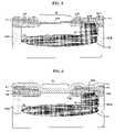
- a spacer oxide layer 41is deposited on the surface of epitaxial layer 13 and field oxide regions 21 A, 21 B, and 21 C. Additionally, P-type isolation regions 42 A and 42 B are formed using conventional ion implantation techniques. Isolation regions 42 A and 42 B serve to electrically isolate the varactor device from other devices that may be formed on the same substrate. Using standard photoresist masking techniques, a portion of spacer oxide layer 41 is selectively removed via a dry and/or wet etch process or other suitable method to expose an implant region 51 (see FIG. 5 ). Implant region 51 represents the region of the semiconductor device where the varactor device of the present invention will be formed. In FIG.
- a base polysilicon layer 61is deposited using one or more methods well known in the art.
- the thickness of base polysilicon layer 61is on the order of about 1800 to 2500 Angstroms.
- a P-type dopantsuch as boron or boron difluoride is then implanted into base polysilicon layer 61 to achieve a peak dopant concentration that preferably is on the order of about 10 18 to 10 20 atoms/cm 3 .
- a base oxide layer 71is deposited on the surface of polysilicon layer 61 .
- Base oxide layer 71preferably has a thickness on the order of about 1800 to 2500 Angstroms.
- an emitter window 81is formed via any suitable method known in the art, including but not limited to, for example, wet or dry etching. Emitter window 81 will later serve to define an emitter region.
- a screen oxide layer 91is formed in the region of emitter window 81 ( FIG. 9 ). Screen oxide layer 91 serves to protect the device from contamination during the ion implantation process employed in the formation of the varactor of the present invention.
- a double-implant varactoris formed in accordance with a preferred embodiment of the present invention.
- the varactor of the present invention as illustratedcomprises the base-emitter junction of a specially optimized NPN device formed with a double base implant.
- a shallow base implant 101is formed using standard ion implantation techniques.
- Shallow base implant 101comprises P-type ions, such as boron, for example, implanted into epitaxial layer 13 .
- the doping profile of shallow base implant 101is optimized for capacitance, leakage current, and tuning range in accordance with a further aspect of the invention described hereinbelow.
- leakage currentmay be maintained below 20 nA at 2.5 V for a 4 pF capacitor (0 V capacitance).
- varactors having significant tuning headroom with a capacitance sensitivity of approximately 17%/V and a three-sigma process variation of only approximately 9%may be achieved.
- Deep base implant 102is then formed using standard ion implantation techniques.
- Deep base implant 102comprises P-type ions, such as boron, for example, implanted into epitaxial layer 13 such that deep base implant 102 is disposed below shallow base implant 101 .
- the doping profile of deep base implant 102is optimized in accordance with a further aspect of the invention described herein to improve Q by reducing the base resistance. For example, in accordance with a preferred embodiment of the present invention, Q of better than 40 may be achieved at 2 GHz.
- an anneal steppreferably is performed.
- base polysilicon layer 61may exhibit some degree of outdiffusion, that is, diffusion into epitaxial layer 13 , wherein outdiffusion regions 103 A and 103 B may be formed. These regions may enhance electrical contact to varactor 100 .
- nitride spacers 111 A, 111 Bare formed on varactor 100 by forming a conformal oxide nitride oxide stack layer (not shown) over the surface of varactor 100 , and then etching away the unwanted portions of the conformal oxide nitride oxide layer using standard techniques.
- Nitride spacers 111 A, 111 Bare not limited to being nitride, but may be any suitable dielectric material (e.g., oxide, oxynitride).
- emitter electrode 121is formed through a series of standard process steps. First, a layer of polysilicon material (not shown) is deposited on the surface of the semiconductor device at a desired thickness, for example, on the order of approximately 2000 Angstroms. Then, a screen oxide layer (not shown) having a thickness on the order of, for example, about 100 to 200 Angstroms, is deposited or thermally grown on the polysilicon layer. Arsenic or similar N-type dopant is implanted into the polysilicon layer through the screen oxide layer to achieve a dopant concentration on the order of about 10 18 to 10 20 atoms/cm 3 . The doped polysilicon layer is then patterned and etched to form emitter electrode 121 as shown in FIG. 12 . A rapid thermal anneal process preferably completes formation of emitter electrode 121 .
- Emitter contact metallizationcommences with the formation of a suitable ohmic contact material, for example, titanium silicide, to form a contact layer 131 on the exposed electrodes of varactor 100 ( FIG. 13 ).
- Base terminal 141 , emitter terminal 142 , and collector terminal 143 contactsare formed using standard metallization processes ( FIG. 14 ).
- Base terminal 141 and emitter terminal 142are contacted using any convenient technique to complete formation of the varactor diode.
- collector terminal 143isolates the emitter-base junction from the substrate, providing flexibility in circuit applications.
- FIG. 15illustrates empirically a simulated as-implanted dopant concentration profile 150 for a varactor formed in accordance with one embodiment of the present invention.
- shallow concentration profile 151illustrates the relationship between net dopant concentration and implant depth for the first, shallow base implant of a preferred varactor.
- Deep concentration profile 152illustrated the relationship between net dopant concentration and implant depth for the second, deep base implant of a preferred varactor.
- shallow concentration profile 151is optimized to achieve high tuning range (i.e., high voltage sensitivity) and low leakage current by minimizing peak dopant concentration 154 and maximizing the slope of the profile.
- Shallow concentration profile 151is thus achieved by simulating a low-dopant, shallow base implant. As implant depth increases, the breadth of shallow concentration profile 151 increases, and thus profile slope decreases. It is therefore preferable to minimize the depth of the first, shallow base implant.
- the maximum extent of the depletion region during varactor operationis identified at junction 161 ( FIG. 16 ).
- deep concentration profile 152may be optimized for Q (i.e., designed to achieve low base resistance) by optimizing peak dopant concentration 155 and depth 162 without significantly changing doping concentration regions more shallow than junction 161 .
- FIG. 17is a flow diagram depicting a method for forming a varactor device on a semiconductor substrate in accordance with one embodiment of the present invention, as described in detail above.
- Step 171comprises providing a semiconductor substrate, such as substrate 11 (see FIG. 1 ) of a suitable semiconductor material.
- Step 172is illustrated in FIGS. 1 through 9 , as described in detail above.
- Steps 173 and 174encompass the formation of the double-implant varactor, as illustrated in FIG. 10 and its accompanying discussion.
- Device metallizationis formed in Step 176 , as illustrated in FIGS. 11 through 14 and their accompanying discussions.
- Steps 175 and 177follow formation of the double-implant varactor (Steps 173 , 174 ) and the device metallization (Step 176 ), respectively.
- Steps 178 and 179comprise optimizing the dopant concentrations and implant energies of the first and second implants of the varactor device in accordance with the optimization methods described herein and illustrated in FIGS. 15 and 16 .
- optimization of deep base implant 102 in relation to shallow base implant 101is performed prior to actual implantation to determine the most desirable parameters for the varactor.
- the as-implanted dopant concentration profile or ion implantation model for each of the two base implantsmay be determined by any convenient technique including, for example, capacitance-voltage techniques such as measuring the reverse-bias capacitance of a P-N junction or a Schottky barrier diode as a function of the applied voltage.
- a more elaborate and preferred methodis the secondary-ion-mass spectroscopy (SIMS) technique, which measures the total impurity profile.
- SIMSsecondary-ion-mass spectroscopy
- an ion beamsputters material off the surface of a semiconductor, and the ion component is detected and mass-analyzed.
- the SIMS techniquehas high sensitivity to many elements such as boron and arsenic, and it is an ideal tool for providing the precision needed for profile measurements in high-concentration or shallow-junction diffusions.
- Another method of obtaining ion implantation modelsis by using the Monte Carlo method. In a Monte Carlo simulation, the ions are followed on their path through the material as they undergo binary collisions with the target atoms. Evaluating the end points of the ion trajectories allows the as-implanted dopant profile to be determined. Once an optimal as-implanted dopant profile is determined for a particular device, ion implantation process parameters may be set to achieve this optimum structure. Process parameters include ion implantation energy and ion concentration.
- a semiconductor devicecan be implemented with various semiconductor technologies and different combinations of known process steps, and that the preferred embodiments and aspects thereof illustrated here are merely exemplary.
- the semiconductor materials, dopant species, and/or concentration of dopants and their concentration profilescan be chosen depending upon the desired properties of the completed device.
Landscapes
- Semiconductor Integrated Circuits (AREA)
- Inductance-Capacitance Distribution Constants And Capacitance-Resistance Oscillators (AREA)
Abstract
Description
Claims (21)
Priority Applications (3)
| Application Number | Priority Date | Filing Date | Title |
|---|---|---|---|
| US09/590,462US6995068B1 (en) | 2000-06-09 | 2000-06-09 | Double-implant high performance varactor and method for manufacturing same |
| AU2001268298AAU2001268298A1 (en) | 2000-06-09 | 2001-06-08 | Double-implant high performance varactor and method for manufacturing same |
| PCT/US2001/018739WO2001095396A2 (en) | 2000-06-09 | 2001-06-08 | Double-implant high performance varactor and method for manufacturing same |
Applications Claiming Priority (1)
| Application Number | Priority Date | Filing Date | Title |
|---|---|---|---|
| US09/590,462US6995068B1 (en) | 2000-06-09 | 2000-06-09 | Double-implant high performance varactor and method for manufacturing same |
Publications (1)
| Publication Number | Publication Date |
|---|---|
| US6995068B1true US6995068B1 (en) | 2006-02-07 |
Family
ID=24362356
Family Applications (1)
| Application Number | Title | Priority Date | Filing Date |
|---|---|---|---|
| US09/590,462Expired - LifetimeUS6995068B1 (en) | 2000-06-09 | 2000-06-09 | Double-implant high performance varactor and method for manufacturing same |
Country Status (3)
| Country | Link |
|---|---|
| US (1) | US6995068B1 (en) |
| AU (1) | AU2001268298A1 (en) |
| WO (1) | WO2001095396A2 (en) |
Cited By (4)
| Publication number | Priority date | Publication date | Assignee | Title |
|---|---|---|---|---|
| US20050161770A1 (en)* | 2004-01-23 | 2005-07-28 | Coolbaugh Douglas D. | Structure and method of hyper-abrupt junction varactors |
| US20070145531A1 (en)* | 2005-12-28 | 2007-06-28 | Dongbu Electronics Co., Ltd. | Semiconductor device and method for manufacturing the same |
| US20150054452A1 (en)* | 2013-08-22 | 2015-02-26 | Maxwave Co., Ltd. | System for Wireless Charging Control Based Magnetic Resonance Type |
| CN110277455A (en)* | 2019-06-17 | 2019-09-24 | 杭州士兰集成电路有限公司 | Semiconductor device and manufacturing method thereof |
Families Citing this family (1)
| Publication number | Priority date | Publication date | Assignee | Title |
|---|---|---|---|---|
| SE0200137L (en) | 2002-01-18 | 2003-07-19 | Ericsson Telefon Ab L M | Production method, varactor and integrated circuit |
Citations (47)
| Publication number | Priority date | Publication date | Assignee | Title |
|---|---|---|---|---|
| US3581164A (en)* | 1968-06-26 | 1971-05-25 | Itt | Junction capacitance component, especially for a monolithic microcircuit |
| US3761319A (en)* | 1970-05-22 | 1973-09-25 | Philips Corp | Methods of manufacturing semiconductor devices |
| US3770519A (en)* | 1970-08-05 | 1973-11-06 | Ibm | Isolation diffusion method for making reduced beta transistor or diodes |
| US3914708A (en) | 1972-11-09 | 1975-10-21 | Hughes Aircraft Co | Bi-state varactor phase modulation network and process for constructing same |
| US4064620A (en) | 1976-01-27 | 1977-12-27 | Hughes Aircraft Company | Ion implantation process for fabricating high frequency avalanche devices |
| JPS53145578A (en)* | 1977-05-25 | 1978-12-18 | Nec Corp | Diode varister |
| US4224733A (en) | 1977-10-11 | 1980-09-30 | Fujitsu Limited | Ion implantation method |
| JPS5626477A (en)* | 1980-02-22 | 1981-03-14 | Sanyo Electric Co Ltd | Variable-capacity diode manufacturing process |
| DE3034287A1 (en)* | 1979-09-14 | 1981-04-16 | Toko, Inc., Tokyo | Varactor semiconductor diode circuit - has semiconductor format to minimise tracking errors in TV and radio receiver applications |
| US4381952A (en) | 1981-05-11 | 1983-05-03 | Rca Corporation | Method for fabricating a low loss varactor diode |
| US4416050A (en) | 1981-09-24 | 1983-11-22 | Rockwell International Corporation | Method of fabrication of dielectrically isolated CMOS devices |
| US4442591A (en) | 1982-02-01 | 1984-04-17 | Texas Instruments Incorporated | High-voltage CMOS process |
| US4727046A (en) | 1986-07-16 | 1988-02-23 | Fairchild Semiconductor Corporation | Method of fabricating high performance BiCMOS structures having poly emitters and silicided bases |
| US4868134A (en)* | 1987-08-31 | 1989-09-19 | Toko, Inc. | Method of making a variable-capacitance diode device |
| US4876211A (en) | 1988-08-09 | 1989-10-24 | Hughes Aircraft Company | Method for fabricating varactor diodes using ion implanation |
| US5010026A (en)* | 1988-08-12 | 1991-04-23 | Sony Corporation | Process for making bipolar transistor |
| US5024955A (en)* | 1989-01-19 | 1991-06-18 | Toko, Inc. | Variable-capacitance diode element having wide capacitance variation range |
| US5069002A (en) | 1991-04-17 | 1991-12-03 | Micron Technology, Inc. | Apparatus for endpoint detection during mechanical planarization of semiconductor wafers |
| JPH0492477A (en)* | 1990-08-08 | 1992-03-25 | Hitachi Ltd | Manufacture of variable capacity diode |
| JPH04177770A (en)* | 1990-11-09 | 1992-06-24 | Nec Corp | Variable capacitance diode and its manufacture |
| JPH04287978A (en)* | 1991-01-10 | 1992-10-13 | Nec Corp | Varactor diode |
| JPH04343479A (en)* | 1991-05-21 | 1992-11-30 | Nec Yamagata Ltd | Variable capacitance diode |
| US5225034A (en) | 1992-06-04 | 1993-07-06 | Micron Technology, Inc. | Method of chemical mechanical polishing predominantly copper containing metal layers in semiconductor processing |
| US5234540A (en) | 1992-04-30 | 1993-08-10 | Submicron Systems, Inc. | Process for etching oxide films in a sealed photochemical reactor |
| US5240522A (en) | 1991-03-29 | 1993-08-31 | Sumitomo Light Metal Industries, Ltd. | Method of producing hardened aluminum alloy sheets having superior thermal stability |
| US5242524A (en) | 1990-05-16 | 1993-09-07 | International Business Machines Corporation | Device for detecting an end point in polishing operations |
| US5314843A (en) | 1992-03-27 | 1994-05-24 | Micron Technology, Inc. | Integrated circuit polishing method |
| US5376483A (en) | 1993-10-07 | 1994-12-27 | Micron Semiconductor, Inc. | Method of making masks for phase shifting lithography |
| US5405790A (en) | 1993-11-23 | 1995-04-11 | Motorola, Inc. | Method of forming a semiconductor structure having MOS, bipolar, and varactor devices |
| US5407526A (en) | 1993-06-30 | 1995-04-18 | Intel Corporation | Chemical mechanical polishing slurry delivery and mixing system |
| US5413941A (en) | 1994-01-06 | 1995-05-09 | Micron Technology, Inc. | Optical end point detection methods in semiconductor planarizing polishing processes |
| US5439553A (en) | 1994-03-30 | 1995-08-08 | Penn State Research Foundation | Controlled etching of oxides via gas phase reactions |
| US5557140A (en)* | 1995-04-12 | 1996-09-17 | Hughes Aircraft Company | Process tolerant, high-voltage, bi-level capacitance varactor diode |
| US5576126A (en) | 1994-09-26 | 1996-11-19 | Micron Technology, Inc. | Phase shifting mask |
| US5578855A (en) | 1994-02-15 | 1996-11-26 | National Semiconductor Corporation | High-voltage CMOS transistors on a standard CMOS wafer |
| US5627402A (en) | 1993-11-25 | 1997-05-06 | Nec Corporation | Variable-capacitance device and semiconductor integrated circuit device having such variable-capacitance device |
| US5637185A (en) | 1995-03-30 | 1997-06-10 | Rensselaer Polytechnic Institute | Systems for performing chemical mechanical planarization and process for conducting same |
| US5648281A (en) | 1992-09-21 | 1997-07-15 | Siliconix Incorporated | Method for forming an isolation structure and a bipolar transistor on a semiconductor substrate |
| US5685951A (en) | 1996-02-15 | 1997-11-11 | Micron Technology, Inc. | Methods and etchants for etching oxides of silicon with low selectivity in a vapor phase system |
| US5691546A (en)* | 1988-12-10 | 1997-11-25 | Canon Kabushiki Kaisha | Semiconductor device having a high current gain and a higher Ge amount at the base region than at the emitter and collector regions, and photoelectric conversion apparatus using the device |
| US5783495A (en) | 1995-11-13 | 1998-07-21 | Micron Technology, Inc. | Method of wafer cleaning, and system and cleaning solution regarding same |
| US5854117A (en) | 1995-09-18 | 1998-12-29 | U.S. Philips Corporation | Method of manufacturing a varicap diode, a varicap diode, a receiver device, and a TV receiver set |
| US5880516A (en)* | 1995-08-31 | 1999-03-09 | Nec Corporation | Semiconductor device utilizing a pedestal collector region and method of manufacturing the same |
| US5965912A (en) | 1997-09-03 | 1999-10-12 | Motorola, Inc. | Variable capacitor and method for fabricating the same |
| US6015726A (en) | 1997-03-24 | 2000-01-18 | Nec Corporation | Semiconductor device and method of producing the same |
| US6103456A (en) | 1998-07-22 | 2000-08-15 | Siemens Aktiengesellschaft | Prevention of photoresist poisoning from dielectric antireflective coating in semiconductor fabrication |
| US20020014650A1 (en)* | 1999-03-03 | 2002-02-07 | Hirotoshi Kubo | High frequency transistor device |
- 2000
- 2000-06-09USUS09/590,462patent/US6995068B1/ennot_activeExpired - Lifetime
- 2001
- 2001-06-08WOPCT/US2001/018739patent/WO2001095396A2/enactiveApplication Filing
- 2001-06-08AUAU2001268298Apatent/AU2001268298A1/ennot_activeAbandoned
Patent Citations (48)
| Publication number | Priority date | Publication date | Assignee | Title |
|---|---|---|---|---|
| US3581164A (en)* | 1968-06-26 | 1971-05-25 | Itt | Junction capacitance component, especially for a monolithic microcircuit |
| US3761319A (en)* | 1970-05-22 | 1973-09-25 | Philips Corp | Methods of manufacturing semiconductor devices |
| US3770519A (en)* | 1970-08-05 | 1973-11-06 | Ibm | Isolation diffusion method for making reduced beta transistor or diodes |
| US3914708A (en) | 1972-11-09 | 1975-10-21 | Hughes Aircraft Co | Bi-state varactor phase modulation network and process for constructing same |
| US4064620A (en) | 1976-01-27 | 1977-12-27 | Hughes Aircraft Company | Ion implantation process for fabricating high frequency avalanche devices |
| JPS53145578A (en)* | 1977-05-25 | 1978-12-18 | Nec Corp | Diode varister |
| US4224733A (en) | 1977-10-11 | 1980-09-30 | Fujitsu Limited | Ion implantation method |
| DE3034287A1 (en)* | 1979-09-14 | 1981-04-16 | Toko, Inc., Tokyo | Varactor semiconductor diode circuit - has semiconductor format to minimise tracking errors in TV and radio receiver applications |
| JPS5642381A (en)* | 1979-09-14 | 1981-04-20 | Toko Inc | Variable capacity diode device |
| JPS5626477A (en)* | 1980-02-22 | 1981-03-14 | Sanyo Electric Co Ltd | Variable-capacity diode manufacturing process |
| US4381952A (en) | 1981-05-11 | 1983-05-03 | Rca Corporation | Method for fabricating a low loss varactor diode |
| US4416050A (en) | 1981-09-24 | 1983-11-22 | Rockwell International Corporation | Method of fabrication of dielectrically isolated CMOS devices |
| US4442591A (en) | 1982-02-01 | 1984-04-17 | Texas Instruments Incorporated | High-voltage CMOS process |
| US4727046A (en) | 1986-07-16 | 1988-02-23 | Fairchild Semiconductor Corporation | Method of fabricating high performance BiCMOS structures having poly emitters and silicided bases |
| US4868134A (en)* | 1987-08-31 | 1989-09-19 | Toko, Inc. | Method of making a variable-capacitance diode device |
| US4876211A (en) | 1988-08-09 | 1989-10-24 | Hughes Aircraft Company | Method for fabricating varactor diodes using ion implanation |
| US5010026A (en)* | 1988-08-12 | 1991-04-23 | Sony Corporation | Process for making bipolar transistor |
| US5691546A (en)* | 1988-12-10 | 1997-11-25 | Canon Kabushiki Kaisha | Semiconductor device having a high current gain and a higher Ge amount at the base region than at the emitter and collector regions, and photoelectric conversion apparatus using the device |
| US5024955A (en)* | 1989-01-19 | 1991-06-18 | Toko, Inc. | Variable-capacitance diode element having wide capacitance variation range |
| US5242524A (en) | 1990-05-16 | 1993-09-07 | International Business Machines Corporation | Device for detecting an end point in polishing operations |
| JPH0492477A (en)* | 1990-08-08 | 1992-03-25 | Hitachi Ltd | Manufacture of variable capacity diode |
| JPH04177770A (en)* | 1990-11-09 | 1992-06-24 | Nec Corp | Variable capacitance diode and its manufacture |
| JPH04287978A (en)* | 1991-01-10 | 1992-10-13 | Nec Corp | Varactor diode |
| US5240522A (en) | 1991-03-29 | 1993-08-31 | Sumitomo Light Metal Industries, Ltd. | Method of producing hardened aluminum alloy sheets having superior thermal stability |
| US5069002A (en) | 1991-04-17 | 1991-12-03 | Micron Technology, Inc. | Apparatus for endpoint detection during mechanical planarization of semiconductor wafers |
| JPH04343479A (en)* | 1991-05-21 | 1992-11-30 | Nec Yamagata Ltd | Variable capacitance diode |
| US5314843A (en) | 1992-03-27 | 1994-05-24 | Micron Technology, Inc. | Integrated circuit polishing method |
| US5234540A (en) | 1992-04-30 | 1993-08-10 | Submicron Systems, Inc. | Process for etching oxide films in a sealed photochemical reactor |
| US5225034A (en) | 1992-06-04 | 1993-07-06 | Micron Technology, Inc. | Method of chemical mechanical polishing predominantly copper containing metal layers in semiconductor processing |
| US5648281A (en) | 1992-09-21 | 1997-07-15 | Siliconix Incorporated | Method for forming an isolation structure and a bipolar transistor on a semiconductor substrate |
| US5407526A (en) | 1993-06-30 | 1995-04-18 | Intel Corporation | Chemical mechanical polishing slurry delivery and mixing system |
| US5376483A (en) | 1993-10-07 | 1994-12-27 | Micron Semiconductor, Inc. | Method of making masks for phase shifting lithography |
| US5405790A (en) | 1993-11-23 | 1995-04-11 | Motorola, Inc. | Method of forming a semiconductor structure having MOS, bipolar, and varactor devices |
| US5627402A (en) | 1993-11-25 | 1997-05-06 | Nec Corporation | Variable-capacitance device and semiconductor integrated circuit device having such variable-capacitance device |
| US5413941A (en) | 1994-01-06 | 1995-05-09 | Micron Technology, Inc. | Optical end point detection methods in semiconductor planarizing polishing processes |
| US5578855A (en) | 1994-02-15 | 1996-11-26 | National Semiconductor Corporation | High-voltage CMOS transistors on a standard CMOS wafer |
| US5439553A (en) | 1994-03-30 | 1995-08-08 | Penn State Research Foundation | Controlled etching of oxides via gas phase reactions |
| US5576126A (en) | 1994-09-26 | 1996-11-19 | Micron Technology, Inc. | Phase shifting mask |
| US5637185A (en) | 1995-03-30 | 1997-06-10 | Rensselaer Polytechnic Institute | Systems for performing chemical mechanical planarization and process for conducting same |
| US5557140A (en)* | 1995-04-12 | 1996-09-17 | Hughes Aircraft Company | Process tolerant, high-voltage, bi-level capacitance varactor diode |
| US5880516A (en)* | 1995-08-31 | 1999-03-09 | Nec Corporation | Semiconductor device utilizing a pedestal collector region and method of manufacturing the same |
| US5854117A (en) | 1995-09-18 | 1998-12-29 | U.S. Philips Corporation | Method of manufacturing a varicap diode, a varicap diode, a receiver device, and a TV receiver set |
| US5783495A (en) | 1995-11-13 | 1998-07-21 | Micron Technology, Inc. | Method of wafer cleaning, and system and cleaning solution regarding same |
| US5685951A (en) | 1996-02-15 | 1997-11-11 | Micron Technology, Inc. | Methods and etchants for etching oxides of silicon with low selectivity in a vapor phase system |
| US6015726A (en) | 1997-03-24 | 2000-01-18 | Nec Corporation | Semiconductor device and method of producing the same |
| US5965912A (en) | 1997-09-03 | 1999-10-12 | Motorola, Inc. | Variable capacitor and method for fabricating the same |
| US6103456A (en) | 1998-07-22 | 2000-08-15 | Siemens Aktiengesellschaft | Prevention of photoresist poisoning from dielectric antireflective coating in semiconductor fabrication |
| US20020014650A1 (en)* | 1999-03-03 | 2002-02-07 | Hirotoshi Kubo | High frequency transistor device |
Non-Patent Citations (2)
| Title |
|---|
| IBM Corporation (NN79013241), "Determination of Doping Profiles by Means of SIMS", IBM Technical Disclosure Bulleting, 1979, vol. 21, Issue No. 8, p. 3241-3242.* |
| Racanelli, M. et al. "BC35: a 0.35mum, 30 GHz, Production RF BiCMOS Technology", Bipolar/BiCMOS Circuits and Technology Meeting, Sep. 1999. |
Cited By (10)
| Publication number | Priority date | Publication date | Assignee | Title |
|---|---|---|---|---|
| US20050161770A1 (en)* | 2004-01-23 | 2005-07-28 | Coolbaugh Douglas D. | Structure and method of hyper-abrupt junction varactors |
| US20050161769A1 (en)* | 2004-01-23 | 2005-07-28 | International Business Machines Corporation | Structure and method for hyper-abrupt junction varactors |
| US7183628B2 (en)* | 2004-01-23 | 2007-02-27 | International Business Machines Corporation | Structure and method of hyper-abrupt junction varactors |
| US20070178656A1 (en)* | 2004-01-23 | 2007-08-02 | International Business Machines Corporation | Structure and method for hyper-abrupt junction varactors |
| US7253073B2 (en)* | 2004-01-23 | 2007-08-07 | International Business Machines Corporation | Structure and method for hyper-abrupt junction varactors |
| US7700453B2 (en) | 2004-01-23 | 2010-04-20 | International Business Machines Corporation | Method for forming hyper-abrupt junction varactors |
| US20070145531A1 (en)* | 2005-12-28 | 2007-06-28 | Dongbu Electronics Co., Ltd. | Semiconductor device and method for manufacturing the same |
| US7674681B2 (en)* | 2005-12-28 | 2010-03-09 | Dongbu Electronics Co., Ltd. | Semiconductor device and method for manufacturing the same |
| US20150054452A1 (en)* | 2013-08-22 | 2015-02-26 | Maxwave Co., Ltd. | System for Wireless Charging Control Based Magnetic Resonance Type |
| CN110277455A (en)* | 2019-06-17 | 2019-09-24 | 杭州士兰集成电路有限公司 | Semiconductor device and manufacturing method thereof |
Also Published As
| Publication number | Publication date |
|---|---|
| AU2001268298A1 (en) | 2001-12-17 |
| WO2001095396A3 (en) | 2002-04-18 |
| WO2001095396A2 (en) | 2001-12-13 |
Similar Documents
| Publication | Publication Date | Title |
|---|---|---|
| US7700453B2 (en) | Method for forming hyper-abrupt junction varactors | |
| US5405790A (en) | Method of forming a semiconductor structure having MOS, bipolar, and varactor devices | |
| EP0792525B1 (en) | A varicap diode and method of manufacturing a varicap diode | |
| US7560798B2 (en) | High performance tapered varactor | |
| JP5044818B2 (en) | Method for forming a one-mask super staircase junction varactor using compensated cathode contact | |
| US6660616B2 (en) | P-i-n transit time silicon-on-insulator device | |
| EP0051902A1 (en) | Semiconductor integrated circuit incorporating an active device and a distributed resistor-capacitor device | |
| KR101013251B1 (en) | MOOS varactors using separation wells | |
| US6559024B1 (en) | Method of fabricating a variable capacity diode having a hyperabrupt junction profile | |
| EP1214737B1 (en) | A method of producing a schottky varicap diode | |
| US6362025B1 (en) | Method of manufacturing a vertical-channel MOSFET | |
| US6995068B1 (en) | Double-implant high performance varactor and method for manufacturing same | |
| TW586212B (en) | Fabrication method, varactor, and integrated circuit | |
| CN117238974B (en) | Ultra-mutation varactor in arithmetic multi-ring region and preparation method thereof | |
| JPH09121025A (en) | Monolithic voltage variable capacitor and manufacturing method thereof | |
| US6825546B1 (en) | CMOS varactor with constant dC/dV characteristic | |
| US20070145435A1 (en) | Mos varactor | |
| EP1139434A2 (en) | Variable capacity diode with hyperabrubt junction profile | |
| US6806152B1 (en) | Retrograde doped buried layer transistor and method for producing the same | |
| KR100395159B1 (en) | Method of manufacturing a BICMOS device using Si-Ge | |
| JPH04262570A (en) | How to fabricate CMOS structures |
Legal Events
| Date | Code | Title | Description |
|---|---|---|---|
| AS | Assignment | Owner name:CONEXANT SYSTEMS, INC., CALIFORNIA Free format text:ASSIGNMENT OF ASSIGNORS INTEREST;ASSIGNORS:RACANELLI, MARCO;HU, CHUN;SHERMAN, PHIL N.;REEL/FRAME:011312/0353;SIGNING DATES FROM 20001113 TO 20001117 | |
| AS | Assignment | Owner name:NEWPORT FAB, LLC, CALIFORNIA Free format text:ASSIGNMENT OF ASSIGNORS INTEREST;ASSIGNOR:CONEXANT SYSTEMS, INC.;REEL/FRAME:012754/0852 Effective date:20020312 | |
| AS | Assignment | Owner name:NEWPORT FAB, LLC, CALIFORNIA Free format text:ASSIGNMENT OF ASSIGNORS INTEREST;ASSIGNOR:CONEXANT SYSTEMS, INC.;REEL/FRAME:013280/0690 Effective date:20020312 | |
| STCF | Information on status: patent grant | Free format text:PATENTED CASE | |
| AS | Assignment | Owner name:WACHOVIA CAPITAL FINANCE CORPORATION (WESTERN),CAL Free format text:FIRST AMENDMENT TO PATENT SECURITY AGREEMENT;ASSIGNOR:NEWPORT FAB, LLC;REEL/FRAME:019111/0295 Effective date:20070228 Owner name:WACHOVIA CAPITAL FINANCE CORPORATION (WESTERN), CA Free format text:FIRST AMENDMENT TO PATENT SECURITY AGREEMENT;ASSIGNOR:NEWPORT FAB, LLC;REEL/FRAME:019111/0295 Effective date:20070228 | |
| FPAY | Fee payment | Year of fee payment:4 | |
| FPAY | Fee payment | Year of fee payment:8 | |
| FEPP | Fee payment procedure | Free format text:PAYER NUMBER DE-ASSIGNED (ORIGINAL EVENT CODE: RMPN); ENTITY STATUS OF PATENT OWNER: LARGE ENTITY Free format text:PAYOR NUMBER ASSIGNED (ORIGINAL EVENT CODE: ASPN); ENTITY STATUS OF PATENT OWNER: LARGE ENTITY | |
| FEPP | Fee payment procedure | Free format text:MAINTENANCE FEE REMINDER MAILED (ORIGINAL EVENT CODE: REM.) | |
| FEPP | Fee payment procedure | Free format text:11.5 YR SURCHARGE- LATE PMT W/IN 6 MO, LARGE ENTITY (ORIGINAL EVENT CODE: M1556) | |
| MAFP | Maintenance fee payment | Free format text:PAYMENT OF MAINTENANCE FEE, 12TH YEAR, LARGE ENTITY (ORIGINAL EVENT CODE: M1553) Year of fee payment:12 | |
| AS | Assignment | Owner name:NEWPORT FAB, LLC DBA JAZZ SEMICONDUCTOR OPERATING COMPANY, CALIFORNIA Free format text:RELEASE BY SECURED PARTY;ASSIGNOR:WELLS FARGO CAPITAL FINANCE, LLC, AS SUCCESSOR BY MERGER TO WACHOVIA CAPITAL FINANCE CORPORATION (WESTERN);REEL/FRAME:065284/0123 Effective date:20230929 |